Wireless Components - Farnell element14 · Product Info Wireless Components Product Info...
52
Wireless Components ASK/FSK Single Conversion Receiver TDA 5211 Version 2.0 Specification May 2001
Transcript of Wireless Components - Farnell element14 · Product Info Wireless Components Product Info...
Wireless Components
ASK/FSK Single Conversion Receiver
TDA 5211 Version 2.0
Specification May 2001

Edition 05.01Published by Infineon Technologies AG,Balanstraße 73,81541 München© Infineon Technologies AG May 2001.All Rights Reserved.Attention please!As far as patents or other rights of third parties are concerned, liability is only assumed for components, not for applications, processes and circuits im-plemented within components or assemblies.The information describes the type of component and shall not be considered as assured characteristics.Terms of delivery and rights to change design reserved.Due to technical requirements components may contain dangerous substances. For information on the types in question please contact your nearest Infineon Technologies Office.Infineon Technologies AG is an approved CECC manufacturer.PackingPlease use the recycling operators known to you. We can also help you – get in touch with your nearest sales office. By agreement we will take packing material back, if it is sorted. You must bear the costs of transport. For packing material that is returned to us unsorted or which we are not obliged to accept, we shall have to invoice you for any costs incurred.Components used in life-support devices or systems must be expressly authorized for such purpose!Critical components1 of the Infineon Technologies AG, may only be used in life-support devices or systems2 with the express written approval of the Infineon Technologies AG.1 A critical component is a component used in a life-support device or system whose failure can reasonably be expected to cause the failure of that life-
support device or system, or to affect its safety or effectiveness of that device or system.2 Life support devices or systems are intended (a) to be implanted in the human body, or (b) to support and/or maintain and sustain human life. If they
fail, it is reasonable to assume that the health of the user may be endangered.
ABM®, AOP®, ARCOFI®, ARCOFI®-BA, ARCOFI®-SP, DigiTape®, EPIC®-1, EPIC®-S, ELIC®, FALC®54, FALC®56, FALC®-E1, FALC®-LH, IDEC®, IOM®, IOM®-1, IOM®-2, IPAT®-2, ISAC®-P, ISAC®-S, ISAC®-S TE, ISAC®-P TE, ITAC®, IWE®, MUSAC®-A, OCTAT®-P, QUAT®-S, SICAT®, SICOFI®, SICOFI®-2, SICOFI®-4, SICOFI®-4µC, SLICOFI® are registered trademarks of Infineon Technologies AG.
ACE™, ASM™, ASP™, POTSWIRE™, QuadFALC™, SCOUT™ are trademarks of Infineon Technologies AG.
Revision History
Current Version: 2.0 as of 18.05.01
Previous Version: 1.1, Dec. 2000
Page(in previ-ous Ver-sion)
Page(in current Version)
Subjects (major changes since last revision)
3-12 3-12 Sec. 3.4.8: max. datarate changed, Sec. 3.4.9: max. output current changed
4-4 4-4 value of a changed to 1.414
4-13 4-13 value for C2 changed to 22nF according to bill of materials, τ2 and T2 changed
5-3 5-3 min. supply current limits added, max. limits changed
5-4 5-4 supply current max. limit changed, min. limit added
5-5 5-5 3VOUT min. & max. limits changed, TAGC typ. & max. values changed
5-6 5-6 Section “SLICER” reworked, max. datarate at given load capacitance quoted, high output voltage limits changed, precharge current: min., max. limits changed
5-7 5-7 PDO load and leakage currents limits and typ. values changed, FSK demodula-tion gain min. limit changed
5-9 5-9 PDWN-current max. limit changed, supply currents min. limits added, max. limits changed, 3VOUT min. & max. limits changed, ITAGC_out limits changed
5-10 5-10 Section “SLICER” reworked, max. datarate at given load capacitance quoted, high output voltage limits changed, precharge current: min., max. limits changed, PDO output voltage removed
5-15 5-15 C18 value changed

Product Info
Product InfoWireless Components
Specification, May 2001
Package
TDA 5211
Product Info
General Description The IC is a very low power consump-tion single chip FSK/ASK Superhet-erodyne Receiver (SHR) for thefrequency band 310 to 350 MHz that ispin compatible with the ASK ReceiverTDA5201. The IC offers a high level ofintegration and needs only a few exter-nal components. The device containsa low noise amplifier (LNA), a doublebalanced mixer, a fully integratedVCO, a PLL synthesiser, a crystaloscillator, a limiter with RSSI genera-tor, a PLL FSK demodulator, a data fil-ter, a data comparator (slicer) and apeak detector. Additionally there is apower down feature to save batterylife.
Features Low supply current (Is = 5.7 mA typ. in FSK mode, Is = 5 mA typ. in ASK mode)
Supply voltage range 5V ±10%
Power down mode with very low supply current (50nA typ.)
FSK and ASK demodulation capa-bility
Fully integrated VCO and PLL Synthesiser
ASK sensitivity better than -110 dBm over specified tempera-ture range (- 40 to +105°C)
Selectable frequency ranges 310-330 MHz and 330-350 MHz
Limiter with RSSI generation, operating at 10.7MHz
Selectable reference frequency
2nd order low pass data filter with external capacitors
Data slicer with self-adjusting threshold
FSK sensitivity better than -102 dBm over specified tempera-ture range (- 40 to +105°C)
Applications Keyless Entry Systems
Remote Control Systems
Alarm Systems
Low Bitrate CommunicationSystems
Ordering InformationType Ordering Code Package
TDA 5211 Q67037-A1147 P-TSSOP-28-1
samples available

1 Table of Contents
1 Table of Contents . . . . . . . . . . . . . . . . . . . . . . . . . . . . . . . . . . . . . . . . . . . . . . . . . . . . . . . . . . . . i
2 Product Description . . . . . . . . . . . . . . . . . . . . . . . . . . . . . . . . . . . . . . . . . . . . . . . . . . . . . . . . . . 1
2.1 Overview. . . . . . . . . . . . . . . . . . . . . . . . . . . . . . . . . . . . . . . . . . . . . . . . . . . . . . . . . . . . . . . 2
2.2 Application . . . . . . . . . . . . . . . . . . . . . . . . . . . . . . . . . . . . . . . . . . . . . . . . . . . . . . . . . . . . . 2
2.3 Features . . . . . . . . . . . . . . . . . . . . . . . . . . . . . . . . . . . . . . . . . . . . . . . . . . . . . . . . . . . . . . . 2
2.4 Package Outlines . . . . . . . . . . . . . . . . . . . . . . . . . . . . . . . . . . . . . . . . . . . . . . . . . . . . . . . . 3
3 Functional Description . . . . . . . . . . . . . . . . . . . . . . . . . . . . . . . . . . . . . . . . . . . . . . . . . . . . . . . . 1
3.1 Pin Configuration . . . . . . . . . . . . . . . . . . . . . . . . . . . . . . . . . . . . . . . . . . . . . . . . . . . . . . . . 2
3.2 Pin Definition and Function. . . . . . . . . . . . . . . . . . . . . . . . . . . . . . . . . . . . . . . . . . . . . . . . . 3
3.3 Functional Block Diagram. . . . . . . . . . . . . . . . . . . . . . . . . . . . . . . . . . . . . . . . . . . . . . . . . . 9
3.4 Functional Blocks . . . . . . . . . . . . . . . . . . . . . . . . . . . . . . . . . . . . . . . . . . . . . . . . . . . . . . . 9
3.4.1 Low Noise Amplifier (LNA) . . . . . . . . . . . . . . . . . . . . . . . . . . . . . . . . . . . . . . . . . . . . . . . . . 9
3.4.2 Mixer. . . . . . . . . . . . . . . . . . . . . . . . . . . . . . . . . . . . . . . . . . . . . . . . . . . . . . . . . . . . . . . . . . 10
3.4.3 PLL Synthesizer . . . . . . . . . . . . . . . . . . . . . . . . . . . . . . . . . . . . . . . . . . . . . . . . . . . . . . . . . 10
3.4.4 Crystal Oscillator . . . . . . . . . . . . . . . . . . . . . . . . . . . . . . . . . . . . . . . . . . . . . . . . . . . . . . . . 10
3.4.5 Limiter. . . . . . . . . . . . . . . . . . . . . . . . . . . . . . . . . . . . . . . . . . . . . . . . . . . . . . . . . . . . . . . . . 11
3.4.6 FSK Demodulator . . . . . . . . . . . . . . . . . . . . . . . . . . . . . . . . . . . . . . . . . . . . . . . . . . . . . . . . 11
3.4.7 Data Filter . . . . . . . . . . . . . . . . . . . . . . . . . . . . . . . . . . . . . . . . . . . . . . . . . . . . . . . . . . . . . . 12
3.4.8 Data Slicer . . . . . . . . . . . . . . . . . . . . . . . . . . . . . . . . . . . . . . . . . . . . . . . . . . . . . . . . . . . . . 12
3.4.9 Peak Detector. . . . . . . . . . . . . . . . . . . . . . . . . . . . . . . . . . . . . . . . . . . . . . . . . . . . . . . . . . . 12
3.4.10 Bandgap Reference Circuitry . . . . . . . . . . . . . . . . . . . . . . . . . . . . . . . . . . . . . . . . . . . . . . . 12

4 Applications . . . . . . . . . . . . . . . . . . . . . . . . . . . . . . . . . . . . . . . . . . . . . . . . . . . . . . . . . . . . . . . . . 1
4.1 Choice of LNA Threshold Voltage and Time Constant. . . . . . . . . . . . . . . . . . . . . . . . . . . . 2
4.2 Data Filter Design. . . . . . . . . . . . . . . . . . . . . . . . . . . . . . . . . . . . . . . . . . . . . . . . . . . . . . . . 4
4.3 Quartz Load Capacitance Calculation . . . . . . . . . . . . . . . . . . . . . . . . . . . . . . . . . . . . . . . . 5
4.4 Quartz Frequency Calculation . . . . . . . . . . . . . . . . . . . . . . . . . . . . . . . . . . . . . . . . . . . . . . 6
4.5 Data Slicer Threshold Generation . . . . . . . . . . . . . . . . . . . . . . . . . . . . . . . . . . . . . . . . . . . 7
4.6 ASK/FSK Switch Functional Description . . . . . . . . . . . . . . . . . . . . . . . . . . . . . . . . . . . . . . 8
4.6.1 FSK Mode. . . . . . . . . . . . . . . . . . . . . . . . . . . . . . . . . . . . . . . . . . . . . . . . . . . . . . . . . . . . . . 8
4.6.2 ASK Mode . . . . . . . . . . . . . . . . . . . . . . . . . . . . . . . . . . . . . . . . . . . . . . . . . . . . . . . . . . . . . 10
4.7 Principle of the Precharge Circuit . . . . . . . . . . . . . . . . . . . . . . . . . . . . . . . . . . . . . . . . . . . . 11
5 Reference . . . . . . . . . . . . . . . . . . . . . . . . . . . . . . . . . . . . . . . . . . . . . . . . . . . . . . . . . . . . . . . . . . . 1
5.1 Electrical Data . . . . . . . . . . . . . . . . . . . . . . . . . . . . . . . . . . . . . . . . . . . . . . . . . . . . . . . . . . 2
5.1.2 Operating Range . . . . . . . . . . . . . . . . . . . . . . . . . . . . . . . . . . . . . . . . . . . . . . . . . . . . . . . . 3
5.1.3 AC/DC Characteristics at TAMB = 25°C . . . . . . . . . . . . . . . . . . . . . . . . . . . . . . . . . . . . . . 4
5.1.4 AC/DC Characteristics at TAMB = -40 to 105°C . . . . . . . . . . . . . . . . . . . . . . . . . . . . . . . . 9
5.2 Test Circuit . . . . . . . . . . . . . . . . . . . . . . . . . . . . . . . . . . . . . . . . . . . . . . . . . . . . . . . . . . . . . 12
5.3 Test Board Layouts . . . . . . . . . . . . . . . . . . . . . . . . . . . . . . . . . . . . . . . . . . . . . . . . . . . . . . 13
5.4 Bill of Materials . . . . . . . . . . . . . . . . . . . . . . . . . . . . . . . . . . . . . . . . . . . . . . . . . . . . . . . . . . 15
5.5 Appendix - Noise Figure and Gain Circles . . . . . . . . . . . . . . . . . . . . . . . . . . . . . . . . . . . . . 17

2 Product Description
2.1 Overview. . . . . . . . . . . . . . . . . . . . . . . . . . . . . . . . . . . . . . . . . . . . . . . 2-22.2 Application . . . . . . . . . . . . . . . . . . . . . . . . . . . . . . . . . . . . . . . . . . . . . 2-22.3 Features . . . . . . . . . . . . . . . . . . . . . . . . . . . . . . . . . . . . . . . . . . . . . . . 2-22.4 Package Outlines . . . . . . . . . . . . . . . . . . . . . . . . . . . . . . . . . . . . . . . . 2-3
Contents of this Chapter
Product Description
TDA 5211
2.1 Overview
The IC is a very low power consumption single chip FSK/ASK SuperheterodyneReceiver (SHR) for receive frequencies between 310 and 350 MHz that is pincompatible to the ASK Receiver TDA5201. The IC offers a high level of integra-tion and needs only a few external components. The device contains a lownoise amplifier (LNA), a double balanced mixer, a fully integrated VCO, a PLLsynthesiser, a crystal oscillator, a limiter with RSSI generator, a PLL FSKdemodulator, a data filter, a data comparator (slicer) and a peak detector. Addi-tionally there is a power down feature to save battery life.
2.2 Application
Keyless Entry Systems
Remote Control Systems
Alarm Systems
Low Bitrate Communication Systems
2.3 Features
Low supply current (Is = 5.7 mA typ.FSK mode, 5mA typ. ASK mode)
Supply voltage range 5V ±10%
Power down mode with very low supply current (50nA typ.)
FSK and ASK demodulation capability
Fully integrated VCO and PLL Synthesiser
RF input sensitivity ASK -113dBm typ. at 25°C, better than -110dBm over complete specified operating temperature range (-40 to +105°C)
RF input sensitivity FSK -105dBm typ. at 25°C, better than -102dBm over complete specified operating temperature range (-40 to +105°C)
Receive frequency range between 310 and 350 MHz
Selectable reference frequency
Limiter with RSSI generation, operating at 10.7MHz
2nd order low pass data filter with external capacitors
Data slicer with self-adjusting threshold
2 - 2Wireless Components Specification, May 2001

Product Description
TDA 5211
2.4 Package Outlines
P_TSSOP_28.EPS
Figure 2-1 P-TSSOP-28-1 package outlines
2 - 3Wireless Components Specification, May 2001
3 Functional Description
3.1 Pin Configuration . . . . . . . . . . . . . . . . . . . . . . . . . . . . . . . . . . . . . . . . 3-23.2 Pin Definition and Function. . . . . . . . . . . . . . . . . . . . . . . . . . . . . . . . . 3-33.3 Functional Block Diagram. . . . . . . . . . . . . . . . . . . . . . . . . . . . . . . . . . 3-93.4 Functional Blocks . . . . . . . . . . . . . . . . . . . . . . . . . . . . . . . . . . . . . . . . 3-9
Contents of this Chapter
Functional Description
TDA 5211
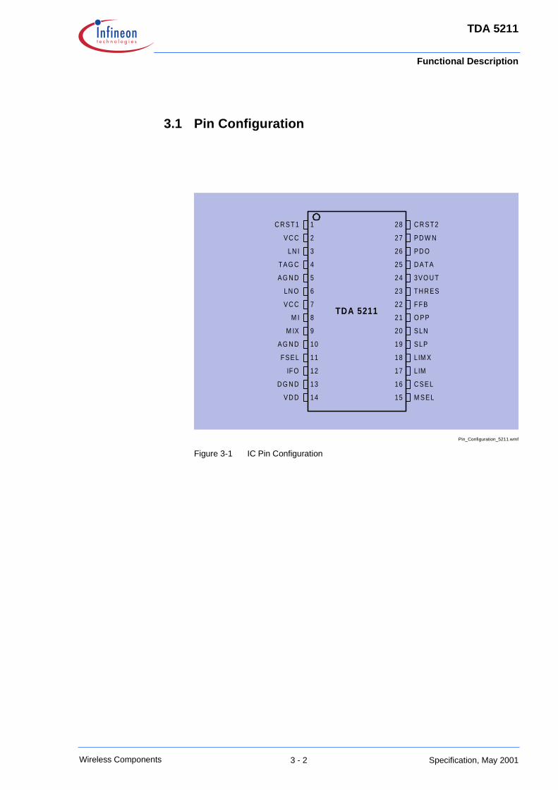
3.1 Pin Configuration
Pin_Configuration_5211.wmf
Figure 3-1 IC Pin Configuration
C R ST 2
PD W N
PD O
D AT A
3VO U T
T H R ES
F F B
O PP
SLN
SLP
LIM X
LIM
C SEL
M SEL
C R ST 1
VC C
LN I
TAG C
AG N D
LN O
VC C
M I
M IX
AG N D
FSEL
IF O
D G N D
VD D
1
2
3
4
5
6
7
8
9
10
11
12
13
14
28
27
26
25
24
23
22
21
20
19
18
17
16
15
TDA 5211
3 - 2Wireless Components Specification, May 2001

Functional Description
TDA 5211
3.2 Pin Definition and Function
In the subsequent table the internal circuits connected to the pins of the deviceare shown. ESD-protection circuits are omitted to ease reading.
.
Table 3-1 Pin Definition and Function
Pin No. Symbol Equivalent I/O-Schematic Function
1 CRST1 External Crystal Connector 1
2 VCC 5V Supply
3 LNI LNA Input
4.15V
50uA
1
57uA
4k
1k
3
500uA
3 - 3Wireless Components Specification, May 2001

Functional Description
TDA 5211
4 TAGC AGC Time Constant Control
5 AGND Analogue Ground Return
6 LNO LNA Output
7 VCC 5V Supply
8
9
MI
MIX
Mixer Input
Complementary Mixer Input
10 AGND Analogue Ground Return
11 FSEL not applicable - has to be left open
1k
3uA
1.4uA
1.7V
4 .3V
4
6
1k
5V
8
1.7V
9
400uA
2k 2k
3 - 4Wireless Components Specification, May 2001
Functional Description
TDA 5211
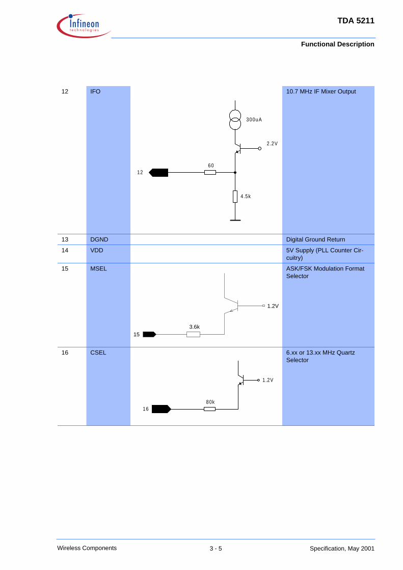
12 IFO 10.7 MHz IF Mixer Output
13 DGND Digital Ground Return
14 VDD 5V Supply (PLL Counter Cir-cuitry)
15 MSEL ASK/FSK Modulation Format Selector
16 CSEL 6.xx or 13.xx MHz Quartz Selector
2.2V
4.5k
6012
300uA
15
1.2V
3.6k
1.2V
80k16
3 - 5Wireless Components Specification, May 2001

Functional Description
TDA 5211
17
18
LIM
LIMX
Limiter Input
Complementary Limiter Input
19 SLP Data Slicer Positive Input
20 SLN Data Slicer Negative Input
21 OPP OpAmp Noninverting Input
330
15k
15k
18
17
2.4V
75uA
19
80µA
15uA
3k100
5uA
20
10k
21200
5uA
3 - 6Wireless Components Specification, May 2001
Functional Description
TDA 5211
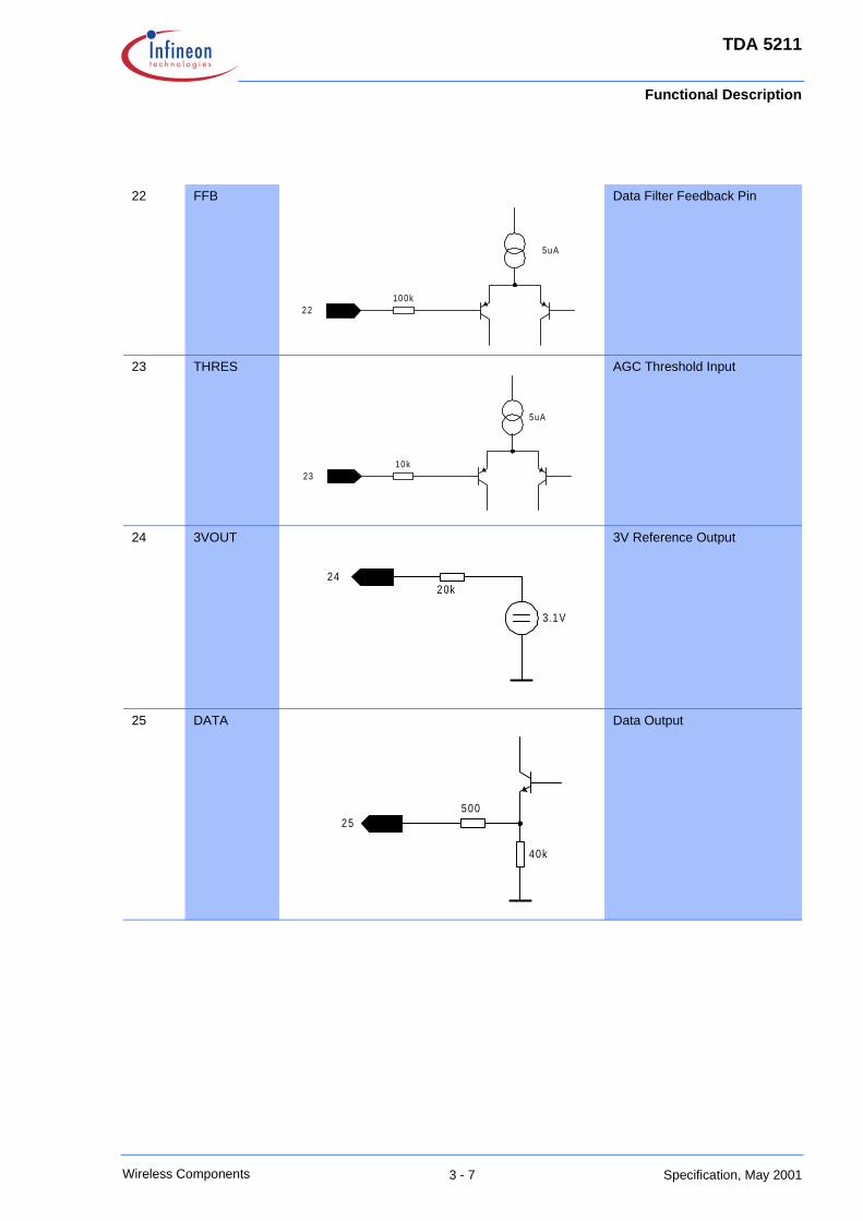
22 FFB Data Filter Feedback Pin
23 THRES AGC Threshold Input
24 3VOUT 3V Reference Output
25 DATA Data Output
100k
5uA
22
10k
5uA
23
3 .1V
2420k
25500
40k
3 - 7Wireless Components Specification, May 2001
Functional Description
TDA 5211
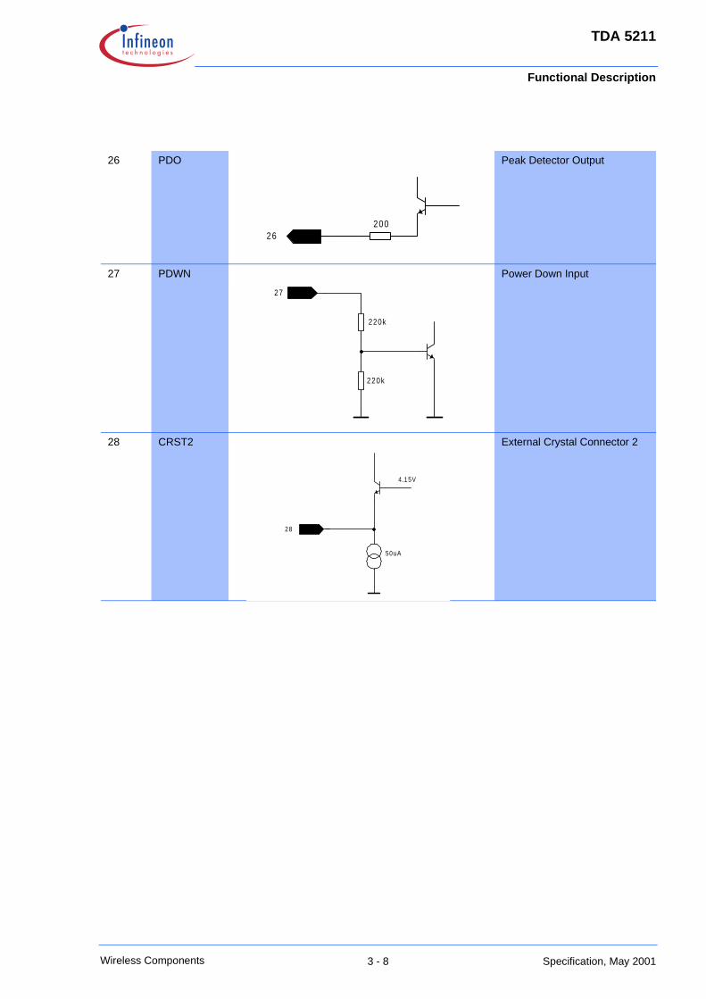
26 PDO Peak Detector Output
27 PDWN Power Down Input
28 CRST2 External Crystal Connector 2
26200
27
220k
220k
4 .15V
50uA
28
3 - 8Wireless Components Specification, May 2001

Functional Description
TDA 5211
3.3 Functional Block Diagram
Functional_diagram_5211.wmf
Figure 3-2 Main Block Diagram
3.4 Functional Blocks
3.4.1 Low Noise Amplifier (LNA)
The LNA is an on-chip cascode amplifier with a voltage gain of 15 to 20dB. Thegain figure is determined by the external matching networks situated ahead ofLNA and between the LNA output LNO (Pin 6) and the Mixer Inputs MI and MIX(Pins 8 and 9). The noise figure of the LNA is approximately 3dB, the currentconsumption is 500µA. The gain can be reduced by approximately 18dB. Theswitching point of this AGC action can be determined externally by applying athreshold voltage at the THRES pin (Pin 23). This voltage is compared internallywith the received signal (RSSI) level generated by the limiter circuitry. In casethat the RSSI level is higher than the threshold voltage the LNA gain is reducedand vice versa. The threshold voltage can be generated by attaching a voltagedivider between the 3VOUT pin (Pin 24) which provides a temperature stable3V output generated from the internal bandgap voltage and the THRES pin asdescribed in Section 4.1. The time constant of the AGC action can be deter-
PDO
: 1 / 2 VCO : 128 / 64 ΦDET
CRYSTALOSC
DATA
Crystal
PDWNCSEL(FSEL)
LoopFilter
BandgapReference
UREF
LNARF
-
+SLICER
TAGC
TDA 5211TDA 5211TDA 5211
VCC
VCC AGND
AGCReference
THRES
3VOUT
FSKPLL Demod
OTA
PEAKDETECTOR
LNI
DGND
-+
MIXLNO MI OPPFFB SLP
VCC
LIM LIMX
IFFilter
IFO SLN
MSEL
LIMITER
6 8 9 12 17 18 22 21 19 20
25
26
23
24
3
4
14
132,7 5,10 11
15
16 1 28 27
-+
ASKFSK
OP
+
-
3 - 9Wireless Components Specification, May 2001

Functional Description
TDA 5211
mined by connecting a capacitor to the TAGC pin (Pin 4) and should be chosenalong with the appropriate threshold voltage according to the intended operat-ing case and interference scenario to be expected during operation. The opti-mum choice of AGC time constant and the threshold voltage is described inSection 4.1.
3.4.2 Mixer
The Double Balanced Mixer downconverts the input frequency (RF) in therange of 310-350MHz to the intermediate frequency (IF) at 10.7MHz with a vol-tage gain of approximately 21dB by utilising either high- or low-side injection ofthe local oscillator signal. In case the mixer is interfaced only single-ended, theunused mixer input has to be tied to ground via a capacitor. The mixer is fol-lowed by a low pass filter with a corner frequency of 20MHz in order to suppressRF signals to appear at the IF output (IFO pin). The IF output is internally con-sisting of an emitter follower that has a source impedance of approximately330Ω to facilitate interfacing the pin directly to a standard 10.7MHz ceramic filterwithout additional matching circuitry.
3.4.3 PLL Synthesizer
The Phase Locked Loop synthesizer consists of a VCO, an asynchronousdivider chain, a phase detector with charge pump and a loop filter and is fullyimplemented on-chip. The VCO is including spiral inductors and varactordiodes. The FSEL pin (Pin11) has to be left open. The tuning range of the VCOwas designed to guarantee over production spread and the specified tempera-ture range a receive frequency range between 310 and 350MHz depending onwhether high- or low-side injection of the local oscillator is used. The oscillatorsignal is fed both to the synthesiser divider chain and to a divider that is dividingthe signal by 2 before it is applied to the downconverting mixer. Local oscillatorhigh side injection has to be used for receive frequencies between approxi-mately 310 and 330 MHz, low side injection for receive frequencies between330 and 350MHz - see also Section 4.4..
3.4.4 Crystal Oscillator
The on-chip crystal oscillator circuitry allows for utilisation of quartzes both inthe 5 and 10MHz range as the overall division ratio of the PLL can be switchedbetween 32 and 64 via the CSEL (Pin 16 ) pin according to the following table.
Table 3-2 CSEL Pin Operating States
CSEL Crystal Frequency
Open 5.xx MHz
Shorted to ground 10.xx MHz
3 - 10Wireless Components Specification, May 2001

Functional Description
TDA 5211
The calculation of the value of the necessary quartz load capacitance is shownin Section 4.3, the quartz frequency calculation is explained in Section 4.4.
3.4.5 Limiter
The Limiter is an AC coupled multistage amplifier with a cumulative gain ofapproximately 80 dB that has a bandpass-characteristic centred around10.7 MHz. It has a typical input impedance of 330 Ω to allow for easy interfacingto a 10.7 MHz ceramic IF filter. The limiter circuit also acts as a Receive SignalStrength Indicator (RSSI) generator which produces a DC voltage that isdirectly proportional to the input signal level as can be seen in Figure 4-2. Thissignal is used to demodulate ASK-modulated receive signals in the subsequentbaseband circuitry. The RSSI output is applied to the modulation format switch,to the Peak Detector input and to the AGC circuitry.
In order to demodulate ASK signals the MSEL pin has to be left open asdescribed in the next chapter.
3.4.6 FSK Demodulator
To demodulate frequency shift keyed (FSK) signals a PLL circuit is used that iscontained fully on chip. The Limiter output differential signal is fed to the linearphase detector as is the output of the 10.7 MHz center frequency VCO. Thedemodulator gain is typically 140µV/kHz. The passive loop filter output that iscomprised fully on chip is fed to both the VCO and the modulation format switchdescribed in more detail below. This signal is representing the demodulated sig-nal with low frequencies applied to the demodulator demodulated to logic onesand high frequencies demodulated to logic zeroes. However this is only valid incase the local oscillator is low-side injected to the mixer which is applicable toreceive frequencies above 330MHz (e.g. 345MHz). In case of receive frequen-cies below 330MHz (e.g.315MHz) high frequencies are demodulated as logicalones due to a sign inversion in the downconversion mixing process. See alsoSection 4.4.
The modulation format switch is actually a switchable amplifier with an AC gainof 11 that is controlled by the MSEL pin (Pin 15) as shown in the following table.This gain was chosen to facilitate detection in the subsequent circuits. The DCgain is 1 in order not to saturate the subsequent Data Filter wih the DC offsetproduced by the demodulator in case of large frequency offsets of the IF signal.The resulting frequency characteristic and details on the principle of operationof the switch are described in Section 4.6.
Table 3-3 MSEL Pin Operating States
MSEL Modulation Format
Open ASK
Shorted to ground FSK
3 - 11Wireless Components Specification, May 2001

Functional Description
TDA 5211
The demodulator circuit is switched off in case of reception of ASK signals.
3.4.7 Data Filter
The data filter comprises an OP-Amp with a bandwidth of 100kHz used as avoltage follower and two 100kΩ on-chip resistors. Along with two externalcapacitors a 2nd order Sallen-Key low pass filter is formed. The selection of thecapacitor values is described in Section 4.2.
3.4.8 Data Slicer
The data slicer is a fast comparator with a bandwidth of 100 kHz. This allowsfor a maximum receive data rate of up to 100kBaud. The maximum achievabledata rate also depends on the IF Filter bandwidth and the local oscillator toler-ance values. Both inputs are accessible. The output delivers a digital data sig-nal (CMOS-like levels) for sbsequent circuits. The self-adjusting threshold onpin 20 its generated by RC-term or peak detector depending on the basebandcoding scheme. The data slicer threshold generation alternatives are describedin more detail in Section 4.5.
3.4.9 Peak Detector
The peak detector generates a DC voltage which is proportional to the peakvalue of the receive data signal. An external RC network is necessary. The inputis connected to the output of the RSSI-output of the Limiter, the output is con-nected to the PDO pin (Pin 26 ). This output can be used as an indicator for thereceived signal strength to use in wake-up circuits and as a reference for thedata slicer in ASK mode. The output current is typically 950µA, the dischargecurrent is lower than 2µA. Note that the RSSI level is also output in case of FSKmode.
3.4.10 Bandgap Reference Circuitry
A Bandgap Reference Circuit provides a temperature stable reference voltagefor the device. A power down mode is available to switch off all subcircuits whichis controlled by the PWDN pin (Pin 27) as shown in the following table. The sup-ply current drawn in this case is typically 50nA.
Table 3-4 PDWN Pin Operating States
PDWN Operating State
Open or tied to ground Powerdown Mode
Tied to Vs Receiver On
3 - 12Wireless Components Specification, May 2001

4 Applications
4.1 Choice of LNA Threshold Voltage and Time Constant . . . . . . . . . . . . 4-24.2 Data Filter Design . . . . . . . . . . . . . . . . . . . . . . . . . . . . . . . . . . . . . . . . 4-44.3 Quartz Load Capacitance Calculation . . . . . . . . . . . . . . . . . . . . . . . . 4-54.4 Quartz Frequency Calculation . . . . . . . . . . . . . . . . . . . . . . . . . . . . . . 4-64.5 Data Slicer Threshold Generation . . . . . . . . . . . . . . . . . . . . . . . . . . . 4-74.6 ASK/FSK Switch Functional Description . . . . . . . . . . . . . . . . . . . . . . 4-84.7 Principle of the Precharge Circuit . . . . . . . . . . . . . . . . . . . . . . . . . . . 4-11
Contents of this Chapter
Applications
TDA 5211
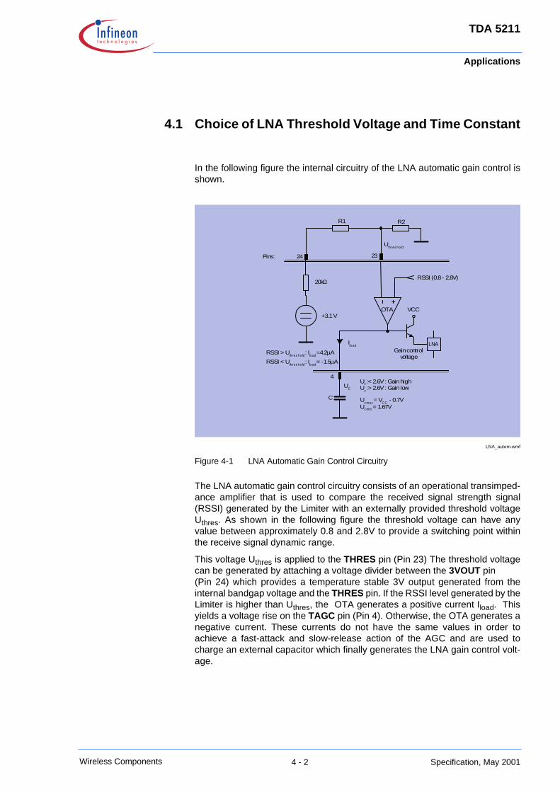
4.1 Choice of LNA Threshold Voltage and Time Constant
In the following figure the internal circuitry of the LNA automatic gain control isshown.
LNA_autom.wmf
Figure 4-1 LNA Automatic Gain Control Circuitry
The LNA automatic gain control circuitry consists of an operational transimped-ance amplifier that is used to compare the received signal strength signal(RSSI) generated by the Limiter with an externally provided threshold voltageUthres. As shown in the following figure the threshold voltage can have anyvalue between approximately 0.8 and 2.8V to provide a switching point withinthe receive signal dynamic range.
This voltage Uthres is applied to the THRES pin (Pin 23) The threshold voltagecan be generated by attaching a voltage divider between the 3VOUT pin (Pin 24) which provides a temperature stable 3V output generated from theinternal bandgap voltage and the THRES pin. If the RSSI level generated by theLimiter is higher than Uthres, the OTA generates a positive current Iload. Thisyields a voltage rise on the TAGC pin (Pin 4). Otherwise, the OTA generates anegative current. These currents do not have the same values in order toachieve a fast-attack and slow-release action of the AGC and are used tocharge an external capacitor which finally generates the LNA gain control volt-age.
4
LNA
RSSI (0.8 - 2.8V)
VCC
Gain controlvoltage
OTA+3.1 V
Iload
RSSI > Uthres ho ld: Iload=4.2µARSSI < Uthres ho ld: Iload= -1.5µA
UC
C
Uc:< 2.6V : Gain highUc:> 2.6V : Gain low
Uc max= VC C - 0.7VUc min = 1.67V
R1 R2
Pins: 24 23
Uthres hold
20kΩ
4 - 2Wireless Components Specification, May 2001
Applications
TDA 5211
RSSI-AGC.wmf
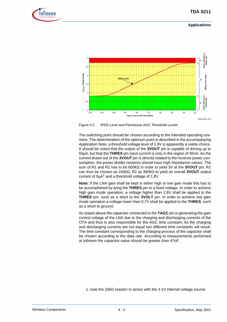
Figure 4-2 RSSI Level and Permissive AGC Threshold Levels
The switching point should be chosen according to the intended operating sce-nario. The determination of the optimum point is described in the accompanyingApplication Note, a threshold voltage level of 1.8V is apparently a viable choice.It should be noted that the output of the 3VOUT pin is capable of driving up to50µA, but that the THRES pin input current is only in the region of 40nA. As thecurrent drawn out of the 3VOUT pin is directly related to the receiver power con-sumption, the power divider resistors should have high impedance values. Thesum of R1 and R2 has to be 600kΩ in order to yield 3V at the 3VOUT pin. R1can thus be chosen as 240kΩ, R2 as 360kΩ to yield an overall 3VOUT outputcurrent of 5µA1 and a threshold voltage of 1.8V
Note: If the LNA gain shall be kept in either high or low gain mode this has tobe accomplished by tying the THRES pin to a fixed voltage. In order to achievehigh gain mode operation, a voltage higher than 2.8V shall be applied to theTHRES pin, such as a short to the 3VOLT pin. In order to achieve low gainmode operation a voltage lower than 0.7V shall be applied to the THRES, suchas a short to ground.
As stated above the capacitor connected to the TAGC pin is generating the gaincontrol voltage of the LNA due to the charging and discharging currents of theOTA and thus is also responsible for the AGC time constant. As the chargingand discharging currents are not equal two different time constants will result.The time constant corresponding to the charging process of the capacitor shallbe chosen according to the data rate. According to measurements performedat Infineon the capacitor value should be greater than 47nF.
1. note the 20kΩ resistor in series with the 3.1V internal voltage source
LNA alw
aysin high gain m
ode
0
0.5
1
1.5
2
2.5
3
-120 -110 -100 -90 -80 -70 -60 -50 -40 -30Input Level at LNA Input [dBm]
UTH
RES
Volta
ge R
ange R
SSI Level RangeLN
A always
in low gain m
ode
RSSI Level
4 - 3Wireless Components Specification, May 2001

Applications
TDA 5211
4.2 Data Filter Design
Utilising the on-board voltage follower and the two 100kΩ on-chip resistors a2nd order Sallen-Key low pass data filter can be constructed by adding 2 exter-nal capacitors between pins 19 (SLP) and 22 (FFB) and to pin 21 (OPP) asdepicted in the following figure and described in the following formulas1.
Filter_Design.wmf
Figure 4-3 Data Filter Design
(1)(2)
with
(3)the quality factor of the poles
where
in case of a Bessel filter a = 1.3617, b = 0.618
and thus Q = 0.577
and in case of a Butterworth filtera = 1.414, b = 1
and thus Q = 0.71
Example: Butterworth filter with f3dB = 5kHz and R = 100kΩ:
C1 = 450pF, C2 = 225pF
1. taken from Tietze/Schenk: Halbleiterschaltungstechnik, Springer Berlin, 1999
Pins: 22 21 19
R R
100k 100k
C1 C2
C1 2Q bR2Π f3dB----------------------= C2 b
4QRΠ f3dB---------------------------=
Q ba
-------=
4 - 4Wireless Components Specification, May 2001
Applications
TDA 5211
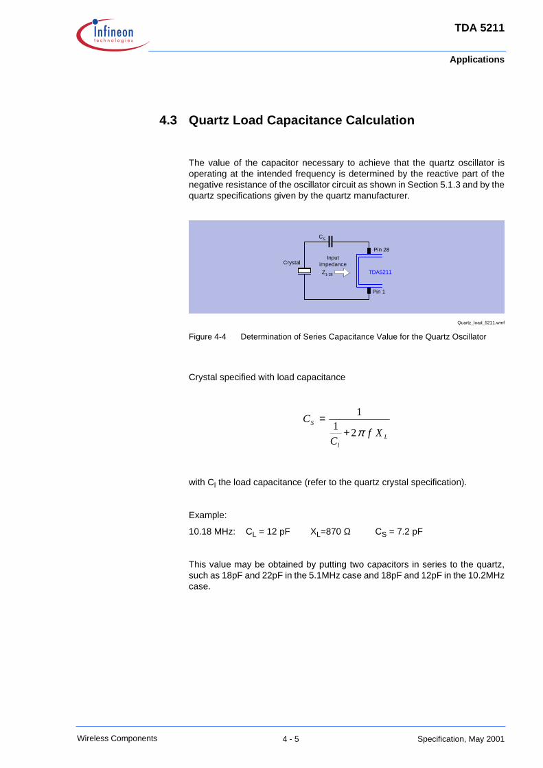
4.3 Quartz Load Capacitance Calculation
The value of the capacitor necessary to achieve that the quartz oscillator isoperating at the intended frequency is determined by the reactive part of thenegative resistance of the oscillator circuit as shown in Section 5.1.3 and by thequartz specifications given by the quartz manufacturer.
Quartz_load_5211.wmf
Figure 4-4 Determination of Series Capacitance Value for the Quartz Oscillator
Crystal specified with load capacitance
with Cl the load capacitance (refer to the quartz crystal specification).
Example:
10.18 MHz: CL = 12 pF XL=870 Ω CS = 7.2 pF
This value may be obtained by putting two capacitors in series to the quartz,such as 18pF and 22pF in the 5.1MHz case and 18pF and 12pF in the 10.2MHzcase.
CS
CrystalInput
impedanceZ1-28 TDA5211
Pin 28
Pin 1
Ll
S
XfC
Cπ211
+=
4 - 5Wireless Components Specification, May 2001

Applications
TDA 5211
4.4 Quartz Frequency Calculation
As described in Section 3.4.3 the operating range of the on-chip VCO is wideenough to guarantee a receive frequency range between 310 and 350MHz. TheVCO signal is divided by 2 before applied to the mixer . This local oscillator sig-nal can be used to downconvert the RF signals both with high- or low-side injec-tion at the mixer. High-side injection of the local oscillator has to be used forreceive frequencies between 310 and 330 MHz. In this case the local oscillatorfrequency is calculated by adding the IF frequency (10.7 MHz) to the RF fre-quency. In this case the higher frequency of a FSK-modulated signal isdemodulated as a logical one (high).
Low-side injection has to be used for receive frequencies between 330 and350 MHz. The local oscillator frequency is calculated by subtracting the IF fre-quency (10.7 MHz) from the RF frequency then. Please note that in this casesign-inversion occurs and the higher frequency of a FSK-modulated signal isdemodulated as a logical zero (low). The overall division ratios in the PLL are64 or 32 depending on whether the CSEL-pin is left open or tied to ground.
Therefore the quartz frequency may be calculated by using the following for-mula:
ƒQU = (ƒRF ± 10.7) / r
with ƒRF receive frequency
ƒLO local oscillator (PLL) frequency (ƒRF ± 10.7)
ƒQU quartz oscillator frequency
r ratio of local oscillator (PLL) frequency and quartz frequency as shown in the subsequent table
This yields the following examples:
CSEL tied to GND:
CSEL open:
Table 4-1 PLL Division Ratio Dependence on States of CSEL
CSEL Ratio r = (fLO/fQU)
open 64
GND 32
( ) MHzMHzMHzf 1781.1032/7.10315QU =+=
( ) MHzMHzMHzf 4469.1032/7.10345QU =−=
( ) MHzMHzMHzf 0891.564/7.10315QU =+=
( ) MHzMHzMHzf 2234.564/7.10345QU =−=
4 - 6Wireless Components Specification, May 2001

Applications
TDA 5211
4.5 Data Slicer Threshold Generation
The threshold of the data slicer can be generated using an external R-C inte-grator as shown in Figure 4-5. The cut-off frequency of the R-C integrator hasto be lower than the lowest frequency appearing in the data signal. In order tokeep distortion low, the minimum value for R is 20kΩ.
Data_slice1.wmf
Figure 4-5 Data Slicer Threshold Generation with External R-C Integrator
In case of ASK operation another possibility for threshold generation is to usethe peak detector in connection with two resistors and one capacitor as shownin the following figure. The component values are depending on the codingscheme and the protocol used.
Data_slice2.wmf
Figure 4-6 Data Slicer Threshold Generation Utilising the Peak Detector
Pins: 2019
R
C
25data out
Uthreshold
data slicer
datafilter
Pins: 2019 25data out
Uthreshold
data slicer
datafilter
26
peak detector
CR
R
4 - 7Wireless Components Specification, May 2001
Applications
TDA 5211
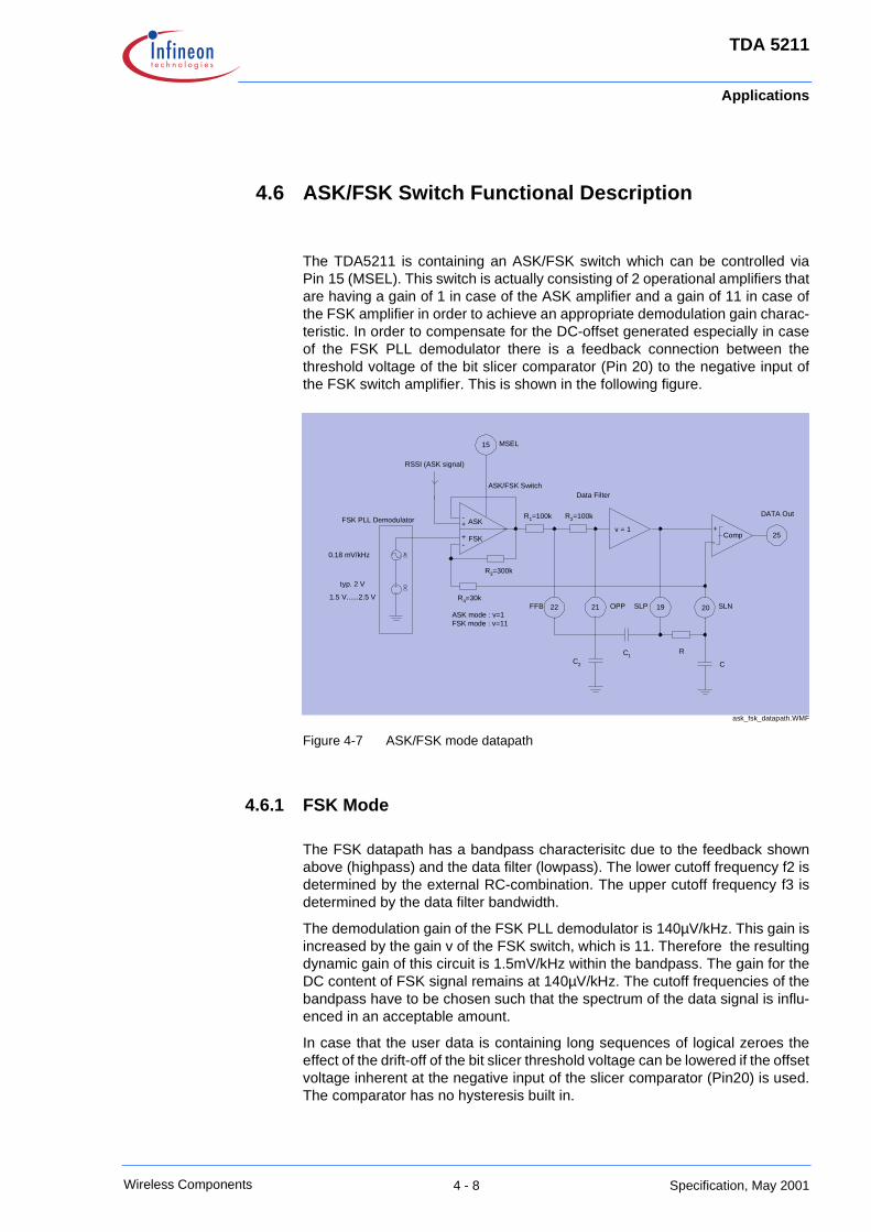
4.6 ASK/FSK Switch Functional Description
The TDA5211 is containing an ASK/FSK switch which can be controlled viaPin 15 (MSEL). This switch is actually consisting of 2 operational amplifiers thatare having a gain of 1 in case of the ASK amplifier and a gain of 11 in case ofthe FSK amplifier in order to achieve an appropriate demodulation gain charac-teristic. In order to compensate for the DC-offset generated especially in caseof the FSK PLL demodulator there is a feedback connection between thethreshold voltage of the bit slicer comparator (Pin 20) to the negative input ofthe FSK switch amplifier. This is shown in the following figure.
ask_fsk_datapath.WMF
Figure 4-7 ASK/FSK mode datapath
4.6.1 FSK Mode
The FSK datapath has a bandpass characterisitc due to the feedback shownabove (highpass) and the data filter (lowpass). The lower cutoff frequency f2 isdetermined by the external RC-combination. The upper cutoff frequency f3 isdetermined by the data filter bandwidth.
The demodulation gain of the FSK PLL demodulator is 140µV/kHz. This gain isincreased by the gain v of the FSK switch, which is 11. Therefore the resultingdynamic gain of this circuit is 1.5mV/kHz within the bandpass. The gain for theDC content of FSK signal remains at 140µV/kHz. The cutoff frequencies of thebandpass have to be chosen such that the spectrum of the data signal is influ-enced in an acceptable amount.
In case that the user data is containing long sequences of logical zeroes theeffect of the drift-off of the bit slicer threshold voltage can be lowered if the offsetvoltage inherent at the negative input of the slicer comparator (Pin20) is used.The comparator has no hysteresis built in.
R1=100k R2=100k
v = 1
19R4=30k
R3=300k
DATA Out
ACD
Ctyp. 2 V
1.5 V......2.5 V
0.18 mV/kHz
FSK PLL Demodulator
RSSI (ASK signal)
C1R
ASK/FSK Switch
ASK
FSK+-
+-
22
25
CC2
20ASK mode : v=1FSK mode : v=11
21
15 MSEL
FFB OPP SLP SLN
Comp-
+
Data Filter
4 - 8Wireless Components Specification, May 2001

Applications
TDA 5211
This offset voltage is generated by the bias current of the negative input of thecomparator (i.e. 20nA) running over the external resistor R. This voltage raisesthe voltage appearing at pin 20 (e.g. 1mV with R = 100kΩ). In order to obtainbenefit of this asymmetrical offset for the demodulation of long zeros the lowerof the two FSK frequencies should be chosen in the transmitter as the zero-symbol frequency.
In the following figure the shape of the above mentioned bandpass is shown.
frequenzgang.WMF
Figure 4-8 Frequency characterstic in case of FSK mode
The cutoff frequencies are calculated with the following formulas:
f3 is the 3dB cutoff frequency of the data filter - see Section 4.2.
Example:
R = 100kΩ, C = 47nF
This leads tof1 = 44Hz and f2 = 485Hz
v
0dB
3dB
v-3dB
f
20dB/dec -40dB/dec
f1 f2 f3
gain (pin19)
DC
0.18mV/kHz 2mV/kHz
CkRkRf
⋅Ω+Ω⋅=
3303302
11
π
112 11 ffvf ⋅=⋅=
dBff 33 =
4 - 9Wireless Components Specification, May 2001

Applications
TDA 5211
4.6.2 ASK Mode
In case the receiver is operated in ASK mode the datapath frequency charac-tersitic is dominated by the data filter alone, thus it is lowpass shaped.The cutofffrequency is determined by the external capacitors C12 and C14 and the inter-nal 100k resistors as described in Section 4.2
freq_ask.WMF
Figure 4-9 Frequency charcteristic in case of ASK mode
0dB
-3dB
f
-40dB/dec
f3dB
4 - 10Wireless Components Specification, May 2001
Applications
TDA 5211
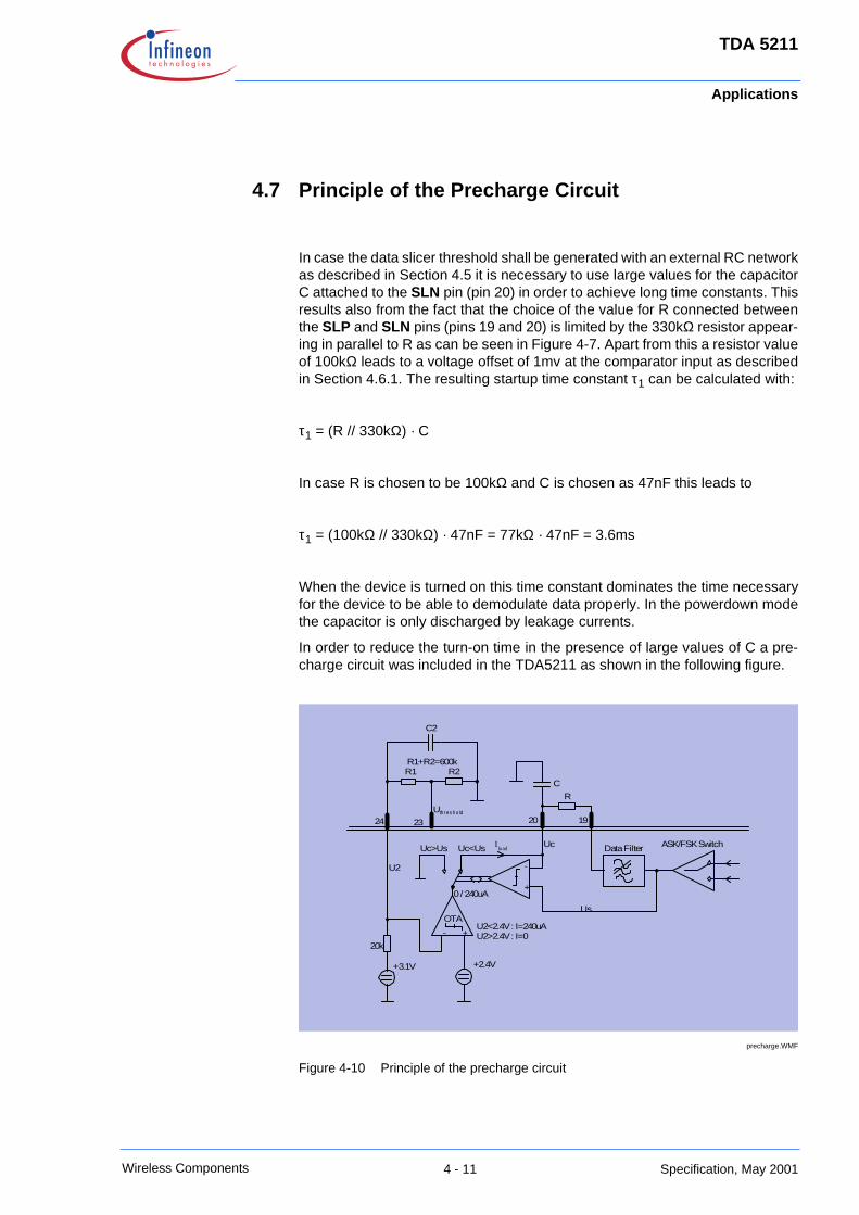
4.7 Principle of the Precharge Circuit
In case the data slicer threshold shall be generated with an external RC networkas described in Section 4.5 it is necessary to use large values for the capacitorC attached to the SLN pin (pin 20) in order to achieve long time constants. Thisresults also from the fact that the choice of the value for R connected betweenthe SLP and SLN pins (pins 19 and 20) is limited by the 330kΩ resistor appear-ing in parallel to R as can be seen in Figure 4-7. Apart from this a resistor valueof 100kΩ leads to a voltage offset of 1mv at the comparator input as describedin Section 4.6.1. The resulting startup time constant τ1 can be calculated with:
τ1 = (R // 330kΩ) · C
In case R is chosen to be 100kΩ and C is chosen as 47nF this leads to
τ1 = (100kΩ // 330kΩ) · 47nF = 77kΩ · 47nF = 3.6ms
When the device is turned on this time constant dominates the time necessaryfor the device to be able to demodulate data properly. In the powerdown modethe capacitor is only discharged by leakage currents.
In order to reduce the turn-on time in the presence of large values of C a pre-charge circuit was included in the TDA5211 as shown in the following figure.
precharge.WMF
Figure 4-10 Principle of the precharge circuit
Iload
+3.1V
20k
+-OTA
+2.4V
R1 R2
24 23Uthres hold
C
0 / 240uA+
-
20 19
R
Data Filter ASK/FSK Switch
C2
U2
Us
UcUc<UsUc>Us
U2<2.4V : I=240uAU2>2.4V : I=0
R1+R2=600k
4 - 11Wireless Components Specification, May 2001
Applications
TDA 5211
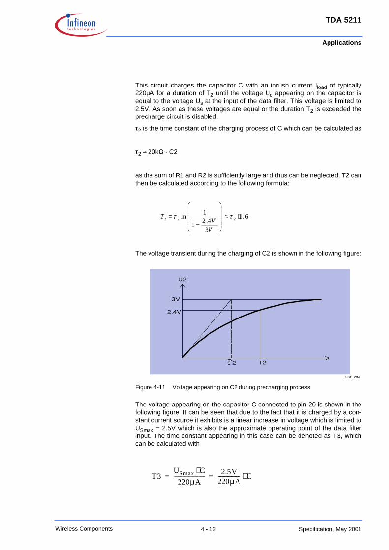
This circuit charges the capacitor C with an inrush current Iload of typically220µA for a duration of T2 until the voltage Uc appearing on the capacitor isequal to the voltage Us at the input of the data filter. This voltage is limited to2.5V. As soon as these voltages are equal or the duration T2 is exceeded theprecharge circuit is disabled.
τ2 is the time constant of the charging process of C which can be calculated as
τ2 ≈ 20kΩ · C2
as the sum of R1 and R2 is sufficiently large and thus can be neglected. T2 canthen be calculated according to the following formula:
The voltage transient during the charging of C2 is shown in the following figure:
e-fkt1.WMF
Figure 4-11 Voltage appearing on C2 during precharging process
The voltage appearing on the capacitor C connected to pin 20 is shown in thefollowing figure. It can be seen that due to the fact that it is charged by a con-stant current source it exhibits is a linear increase in voltage which is limited toUSmax = 2.5V which is also the approximate operating point of the data filterinput. The time constant appearing in this case can be denoted as T3, whichcan be calculated with
6.1
34.21
1ln 222 ⋅≈
−= ττ
VVT
U2
2
3V
2.4V
T2
T3USmax C⋅
220µA------------------------
2.5V220µA----------------- C⋅= =
4 - 12Wireless Components Specification, May 2001

Applications
TDA 5211
e-Fkt2.WMF
Figure 4-12 Voltage transient on capacitor C attached to pin 20
As an example the choice of C2 = 22nF and C = 47nF yields
τ2 = 0.44ms
T2 = 0.71ms
T3 = 0.53ms
This means that in this case the inrush current could flow for a duration of0.64ms but stops already after 0.49ms when the USmax limit has been reached.T3 should always be chosen to be shorter than T2.
It has to be noted finally that during the turn-on duration T2 the overall devicepower consumption is increased by the 220µA needed to charge C.
The precharge circuit may be disabled if C2 is not equipped. This yields a T2close to zero. Note that the sum of R4 and R5 has to be 600kΩ in order to pro-duce 3V at the THRES pin as this voltage is internally used also as the refer-ence for the FSK demodulator.
Us
T3
Uc
4 - 13Wireless Components Specification, May 2001

5 Reference
5.1 Electrical Data. . . . . . . . . . . . . . . . . . . . . . . . . . . . . . . . . . . . . . . . . . . 5-25.2 Test Circuit . . . . . . . . . . . . . . . . . . . . . . . . . . . . . . . . . . . . . . . . . . . . 5-115.3 Test Board Layouts. . . . . . . . . . . . . . . . . . . . . . . . . . . . . . . . . . . . . . 5-125.4 Bill of Materials . . . . . . . . . . . . . . . . . . . . . . . . . . . . . . . . . . . . . . . . . 5-14
Contents of this Chapter
Reference
TDA 5211preliminary
5.1 Electrical Data
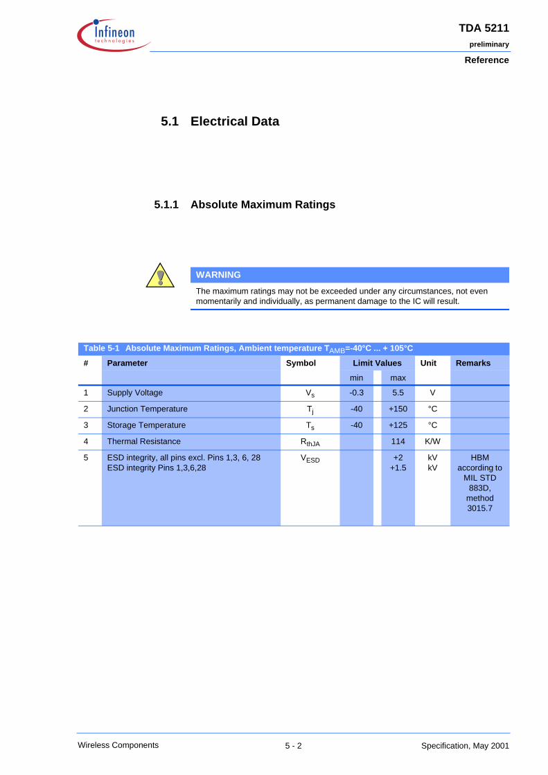
5.1.1 Absolute Maximum Ratings
WARNING
The maximum ratings may not be exceeded under any circumstances, not even momentarily and individually, as permanent damage to the IC will result.
Table 5-1 Absolute Maximum Ratings, Ambient temperature TAMB=-40°C ... + 105°C
# Parameter Symbol Limit Values Unit Remarks
min max
1 Supply Voltage Vs -0.3 5.5 V
2 Junction Temperature Tj -40 +150 °C
3 Storage Temperature Ts -40 +125 °C
4 Thermal Resistance RthJA 114 K/W
5 ESD integrity, all pins excl. Pins 1,3, 6, 28ESD integrity Pins 1,3,6,28
VESD +2+1.5
kVkV
HBM according to
MIL STD 883D,
method 3015.7
5 - 2Wireless Components Specification, May 2001
Reference
TDA 5211preliminary
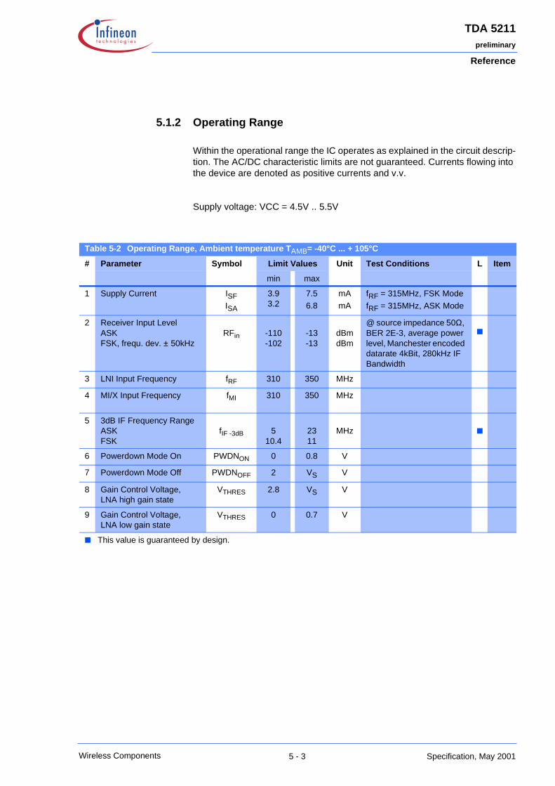
5.1.2 Operating Range
Within the operational range the IC operates as explained in the circuit descrip-tion. The AC/DC characteristic limits are not guaranteed. Currents flowing into the device are denoted as positive currents and v.v.
Supply voltage: VCC = 4.5V .. 5.5V
Table 5-2 Operating Range, Ambient temperature TAMB= -40°C ... + 105°C
# Parameter Symbol Limit Values Unit Test Conditions L Item
min max
1 Supply Current ISFISA
3.93.2
7.5
6.8
mA
mA
fRF = 315MHz, FSK Mode
fRF = 315MHz, ASK Mode
2 Receiver Input Level ASKFSK, frequ. dev. ± 50kHz
RFin -110-102
-13-13
dBmdBm
@ source impedance 50Ω, BER 2E-3, average power level, Manchester encoded datarate 4kBit, 280kHz IF Bandwidth
3 LNI Input Frequency fRF 310 350 MHz
4 MI/X Input Frequency fMI 310 350 MHz
5 3dB IF Frequency RangeASKFSK
fIF -3dB 510.4
2311
MHz
6 Powerdown Mode On PWDNON 0 0.8 V
7 Powerdown Mode Off PWDNOFF 2 VS V
8 Gain Control Voltage,LNA high gain state
VTHRES 2.8 VS V
9 Gain Control Voltage,LNA low gain state
VTHRES 0 0.7 V
This value is guaranteed by design.
5 - 3Wireless Components Specification, May 2001

Reference
TDA 5211preliminary
5.1.3 AC/DC Characteristics at TAMB = 25°C
AC/DC characteristics involve the spread of values guaranteed within the spe-cified voltage and ambient temperature range. Typical characteristics are themedian of the production. Currents flowing into the device are denoted as po-sitive currents and vice versa.
The device performance parameters marked with were measured on anInfineon evaluation board as described in Section 5.2.
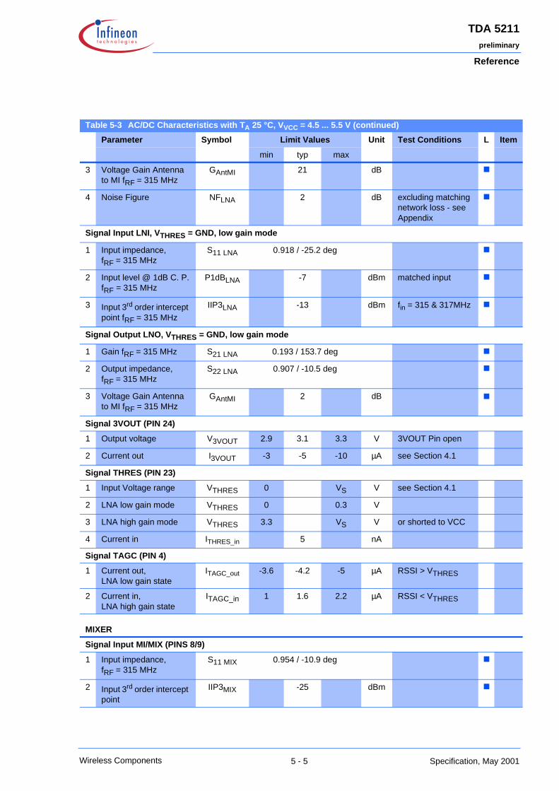
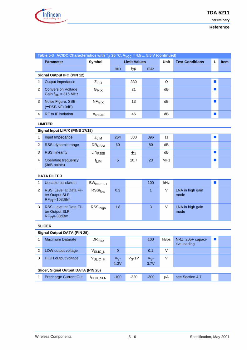
Table 5-3 AC/DC Characteristics with TA 25 °C, VVCC = 4.5 ... 5.5 V
Parameter Symbol Limit Values Unit Test Conditions L Item
min typ max
Supply
Supply Current
1 Supply current,standby mode
IS PDWN 50 100 nA Pin 27 (PDWN) open or tied to 0 V
2 Supply current, device operating in FSK mode
ISF 4.9 5.7 6.5 mA Pin 11 (FSEL) open, Pin 15
(MSEL) tied to GND
3 Supply current, device operating in ASK mode
ISA 4.2 5 5.8 mA Pin 11 (FSEL) open, Pin 15 (MSEL) open
LNA
Signal Input LNI (PIN 3), VTHRES > 2.8V, high gain mode
1 Average Power Level at BER = 2E-3(Sensitivity)
RFin -113 dBm Manchester encoded datarate 4kBit, 280kHz IF Bandwidth
2 Average Power Level at BER = 2E-3(Sensitivity) FSK
RFin -105 dBm Manchester enc. datarate 4kBit, 280kHz IF Bandw., ± 50kHz pk. dev.
3 Input impedance, fRF = 315 MHz
S11 LNA 0.895 / -25.5 deg
4 Input level @ 1dB C.P.fRF=315 MHz
P1dBLNA -14 dBm
5 Input 3rd order intercept point fRF = 315 MHz
IIP3LNA -10 dBm fin = 315 & 317MHz
6 LO signal feedthrough at antenna port
LOLNI -119 dBm
Signal Output LNO (PIN 6), VTHRES > 2.8V, high gain mode
1 Gain fRF = 315 MHz S21 LNA 1.577 / 150.3 deg
2 Output impedance, fRF = 315 MHz
S22 LNA 0.897 / -10.3 deg
5 - 4Wireless Components Specification, May 2001
Reference
TDA 5211preliminary
Table 5-3 AC/DC Characteristics with TA 25 °C, VVCC = 4.5 ... 5.5 V (continued)
Parameter Symbol Limit Values Unit Test Conditions L Item
min typ max
3 Voltage Gain Antenna to MI fRF = 315 MHz
GAntMI 21 dB
4 Noise Figure NFLNA 2 dB excluding matching network loss - see Appendix
Signal Input LNI, VTHRES = GND, low gain mode
1 Input impedance, fRF = 315 MHz
S11 LNA 0.918 / -25.2 deg
2 Input level @ 1dB C. P.fRF = 315 MHz
P1dBLNA -7 dBm matched input
3 Input 3rd order intercept point fRF = 315 MHz
IIP3LNA -13 dBm fin = 315 & 317MHz
Signal Output LNO, VTHRES = GND, low gain mode
1 Gain fRF = 315 MHz S21 LNA 0.193 / 153.7 deg
2 Output impedance, fRF = 315 MHz
S22 LNA 0.907 / -10.5 deg
3 Voltage Gain Antenna to MI fRF = 315 MHz
GAntMI 2 dB
Signal 3VOUT (PIN 24)
1 Output voltage V3VOUT 2.9 3.1 3.3 V 3VOUT Pin open
2 Current out I3VOUT -3 -5 -10 µA see Section 4.1
Signal THRES (PIN 23)
1 Input Voltage range VTHRES 0 VS V see Section 4.1
2 LNA low gain mode VTHRES 0 0.3 V
3 LNA high gain mode VTHRES 3.3 VS V or shorted to VCC
4 Current in ITHRES_in 5 nA
Signal TAGC (PIN 4)
1 Current out,LNA low gain state
ITAGC_out -3.6 -4.2 -5 µA RSSI > VTHRES
2 Current in, LNA high gain state
ITAGC_in 1 1.6 2.2 µA RSSI < VTHRES
MIXER
Signal Input MI/MIX (PINS 8/9)
1 Input impedance, fRF = 315 MHz
S11 MIX 0.954 / -10.9 deg
2 Input 3rd order intercept point
IIP3MIX -25 dBm
5 - 5Wireless Components Specification, May 2001
Reference
TDA 5211preliminary
Table 5-3 AC/DC Characteristics with TA 25 °C, VVCC = 4.5 ... 5.5 V (continued)
Parameter Symbol Limit Values Unit Test Conditions L Item
min typ max
Signal Output IFO (PIN 12)
1 Output impedance ZIFO 330 Ω
2 Conversion Voltage Gain fRF = 315 MHz
GMIX 21 dB
3 Noise Figure, SSB
(~DSB NF+3dB)
NFMIX 13 dB
4 RF to IF isolation ARF-IF 46 dB
LIMITER
Signal Input LIM/X (PINS 17/18)
1 Input Impedance ZLIM 264 330 396 Ω
2 RSSI dynamic range DRRSSI 60 80 dB
3 RSSI linearity LINRSSI ±1 dB
4 Operating frequency (3dB points)
fLIM 5 10.7 23 MHz
DATA FILTER
1 Useable bandwidth BWBB FILT 100 kHz
2 RSSI Level at Data Fil-ter Output SLP, RFIN=-103dBm
RSSIlow 0.3 1 V LNA in high gain mode
3 RSSI Level at Data Fil-ter Output SLP, RFIN=-30dBm
RSSIhigh 1.8 3 V LNA in high gain mode
SLICER
Signal Output DATA (PIN 25)
1 Maximum Datarate DRmax 100 kBps NRZ, 20pF capaci-tive loading
2 LOW output voltage VSLIC_L 0 0.1 V
3 HIGH output voltage VSLIC_H VS-
1.3V
VS-1V VS-
0.7V
V
Slicer, Signal Output DATA (PIN 20)
1 Precharge Current Out IPCH_SLN -100 -220 -300 µA see Section 4.7
5 - 6Wireless Components Specification, May 2001

Reference
TDA 5211preliminary
Table 5-3 AC/DC Characteristics with TA 25 °C, VVCC = 4.5 ... 5.5 V (continued)
Parameter Symbol Limit Values Unit Test Conditions L Item
min typ max
PEAK DETECTOR
Signal Output PDO (PIN 26)
1 Load current Iload -600 -950 -1300 µA
2 Leakage current Ileakage 0 200 1000 nA
CRYSTAL OSCILLATOR
Signals CRSTL1, CRISTL 2, (PINS 1/28)
1 Operating frequency fCRSTL 5 11 MHz fundamental mode, series resonance
2 Input Impedance @ ~5MHz
Z1-28 -850 +j 625
Ω
3 Input Impedance @ ~10MHz
Z1-28 -700 +j 865
Ω
4 Serial Capacity @ ~5MHz
CS 5=C1 9.7 pF
5 Serial Capacity @ ~10MHz
CS10=C1 7.2 pF
ASK/FSK Signal Switch
Signal MSEL (PIN 15)
1 ASK Mode VMSEL 1.4 4 V or open
2 FSK Mode VMSEL 0 0.2 V or tied to ground
FSK DEMODULATOR
1 Demodulation Gain GFMDEM 85 140 225 µV/kHz
2 Useable IF Bandwidth BWIFPLL 10.2 10.7 11.2 MHz
POWER DOWN MODE
Signal PDWN (PIN 27)
1 Powerdown Mode On PWDNON 0 0.8 V
2 Powerdown Mode Off PWDNOff 2.8 VS V
3 Input bias current PDWN
IPDWN 19 µA Power On Mode
4 Start-up Time until valid IF signal is detected
TSU 1 ms
5 - 7Wireless Components Specification, May 2001

Reference
TDA 5211preliminary
Table 5-3 AC/DC Characteristics with TA 25 °C, VVCC = 4.5 ... 5.5 V (continued)
Parameter Symbol Limit Values Unit Test Conditions L Item
min typ max
PLL DIVIDER
Signal CSEL (PIN 16)
1 fCRSTL range 5.xxMHz VCSEL 1.4 4 V or open
2 fCRSTL range
10.xxMHz
VCSEL 0 0.2 V
3 Input bias current CSEL
ICSEL -3 -5 -7 µA CSEL tied to GND
Measured only in lab.
5 - 8Wireless Components Specification, May 2001

Reference
TDA 5211preliminary
5.1.4 AC/DC Characteristics at TAMB = -40 to 105°C
Currents flowing into the device are denoted as positive currents and vice versa.
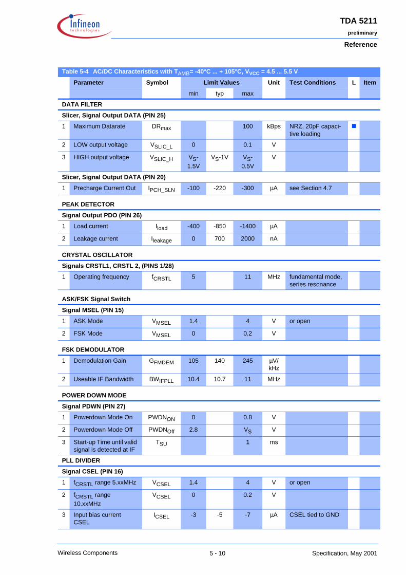
Table 5-4 AC/DC Characteristics with TAMB= -40°C ... + 105°C, VVCC = 4.5 ... 5.5 V
Parameter Symbol Limit Values Unit Test Conditions L Item
min typ max
Supply
Supply Current
1 Supply current,standby mode
IS PDWN 50 400 nA Pin 27 (PDWN) open or tied to 0 V
2 Supply current, device operating in FSK mode
ISF 3.9 5.7 7.5 mA Pin 11 (FSEL) tied to GND, Pin 15
(MSEL) tied to GND
3 Supply current, device operating in ASK mode
ISA 3.2 5 6.8 mA Pin 11 (FSEL) open, Pin 15 (MSEL) open
Signal 3VOUT (PIN 24)
1 Output voltage V3VOUT 2.9 3.1 3.3 V 3VOUT Pin open
2 Current out I3VOUT -3 -5 -10 µA see Section 4.1
Signal THRES (PIN 23)
1 Input Voltage range VTHRES 0 VS-1V V see Section 4.1
2 LNA low gain mode VTHRES 0 0.3 V
3 LNA high gain mode VTHRES 3 VS V or shorted to Pin 24
4 Current in ITHRES_in 5 nA
Signal TAGC (PIN 4)
1 Current out,LNA low gain state
ITAGC_out -1 -4.2 -8 µA RSSI > VTHRES
2 Current in, LNA high gain state
VTAGC_in 0.5 1.5 5 µA RSSI < VTHRES
MIXER
1 Conversion Voltage Gain fRF = 315 MHz
GMIX +19 dB
LIMITER
Signal Input LIM/X (PINS 17/18)
1 RSSI dynamic range DRRSSI 60 80 dB
2 RSSI Level at Data Fil-ter Output SLP, RFIN= -103dBm
RSSIlow 0.3 1 V LNA in high gain mode
3 RSSI Level at Data Fil-ter Output SLP, RFIN= -30dBm
RSSIhigh 1.8 3 V LNA in high gain mode
5 - 9Wireless Components Specification, May 2001
Reference
TDA 5211preliminary
Table 5-4 AC/DC Characteristics with TAMB= -40°C ... + 105°C, VVCC = 4.5 ... 5.5 V
Parameter Symbol Limit Values Unit Test Conditions L Item
min typ max
DATA FILTER
Slicer, Signal Output DATA (PIN 25)
1 Maximum Datarate DRmax 100 kBps NRZ, 20pF capaci-tive loading
2 LOW output voltage VSLIC_L 0 0.1 V
3 HIGH output voltage VSLIC_H VS-
1.5V
VS-1V VS-
0.5V
V
Slicer, Signal Output DATA (PIN 20)
1 Precharge Current Out IPCH_SLN -100 -220 -300 µA see Section 4.7
PEAK DETECTOR
Signal Output PDO (PIN 26)
1 Load current Iload -400 -850 -1400 µA
2 Leakage current Ileakage 0 700 2000 nA
CRYSTAL OSCILLATOR
Signals CRSTL1, CRSTL 2, (PINS 1/28)
1 Operating frequency fCRSTL 5 11 MHz fundamental mode, series resonance
ASK/FSK Signal Switch
Signal MSEL (PIN 15)
1 ASK Mode VMSEL 1.4 4 V or open
2 FSK Mode VMSEL 0 0.2 V
FSK DEMODULATOR
1 Demodulation Gain GFMDEM 105 140 245 µV/kHz
2 Useable IF Bandwidth BWIFPLL 10.4 10.7 11 MHz
POWER DOWN MODE
Signal PDWN (PIN 27)
1 Powerdown Mode On PWDNON 0 0.8 V
2 Powerdown Mode Off PWDNOff 2.8 VS V
3 Start-up Time until valid signal is detected at IF
TSU 1 ms
PLL DIVIDER
Signal CSEL (PIN 16)
1 fCRSTL range 5.xxMHz VCSEL 1.4 4 V or open
2 fCRSTL range
10.xxMHz
VCSEL 0 0.2 V
3 Input bias current CSEL
ICSEL -3 -5 -7 µA CSEL tied to GND
5 - 10Wireless Components Specification, May 2001
Reference
TDA 5211preliminary
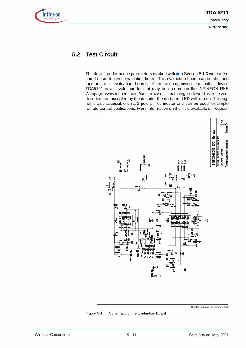
5.2 Test Circuit
The device performance parameters marked with in Section 5.1.3 were mea-sured on an Infineon evaluation board. This evaluation board can be obtainedtogether with evaluation boards of the accompanying transmitter deviceTDA5101 in an evaluation kit that may be ordered on the INFINEON RKEWebpage www.infineon.com/rke. In case a matching codeword is received,decoded and accepted by the decoder the on-board LED will turn on. This sig-nal is also accessible on a 2-pole pin connector and can be used for simpleremote-control applications. More information on the kit is available on request.
TDA521x_testboard_20_schematic.WMF
Figure 5-1 Schematic of the Evaluation Board
5 - 11Wireless Components Specification, May 2001

Reference
TDA 5211preliminary
5.3 Test Board Layouts
tda521x_testboard_20_top.WMF
Figure 5-2 Top Side of the Evaluation Board
tda521x_testboard_20_bot.WMF
Figure 5-3 Bottom Side of the Evaluation Board
5 - 12Wireless Components Specification, May 2001
Reference
TDA 5211preliminary
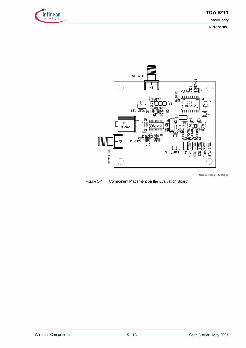
tda521x_testboard_20_plc.EMF
Figure 5-4 Component Placement on the Evaluation Board
5 - 13Wireless Components Specification, May 2001

Reference
TDA 5211preliminary
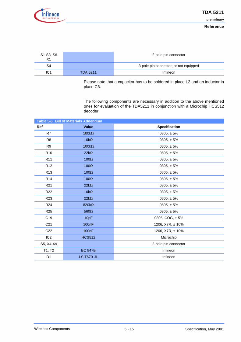
5.4 Bill of Materials
The following components are necessary for evaluation of the TDA5211 at315 MHz without use of a Microchip HCS512 decoder.
Table 5-5 Bill of Materials
Ref Value Specification
R1 100kΩ 0805, ± 5%
R2 100kΩ 0805, ± 5%
R3 820kΩ 0805, ± 5%
R4 240kΩ 0805, ± 5%
R5 360kΩ 0805, ± 5%
R6 10kΩ 0805, ± 5%
L1 15nH Toko, PTL2012-F15N0G
L2 12pF 0805,COG, ± 2%
C1 3.3 pF 0805, COG, ± 0.1pF
C2 10pF 0805, COG, ± 0.1pF
C3 6.8pF 0805, COG, ± 0.1pF
C4 100pF 0805, COG, ± 5%
C5 47nF 1206, X7R, ± 10%
C6 15nH Toko, PTL2012-F15N0G
C7 100pF 0805, COG, ± 5%
C8 33pF 0805, COG, ± 5%
C9 100pF 0805, COG, ± 5%
C10 10nF 0805, X7R, ± 10%
C11 10nF 0805, X7R, ± 10%
C12 220pF 0805, COG, ± 5%
C13 47nF 0805, X7R, ± 10%
C14 470pF 0805, COG, ± 5%
C15 47nF 0805, COG, ± 5%
C16 12pF 0805, COG, ± 1%
C17 18pF 0805, COG, ± 1%
C18 22nF 0805, X7R, ± 5%
Q1 (315 + 10.7MHz)/32 HC49/U, fundamental mode, CL = 12pF,
e.g. 315 MHz: Jauch Q 10,178130-S11-1017-12-10/20
Q2 SFE10.7MA5-A Murata
X2, X3 142-0701-801 Johnson
5 - 14Wireless Components Specification, May 2001
Reference
TDA 5211preliminary
Please note that a capacitor has to be soldered in place L2 and an inductor inplace C6.
The following components are necessary in addition to the above mentionedones for evaluation of the TDA5211 in conjunction with a Microchip HCS512decoder.
S1-S3, S6X1
2-pole pin connector
S4 3-pole pin connector, or not equipped
IC1 TDA 5211 Infineon
Table 5-6 Bill of Materials Addendum
Ref Value Specification
R7 100kΩ 0805, ± 5%
R8 10kΩ 0805, ± 5%
R9 100kΩ 0805, ± 5%
R10 22kΩ 0805, ± 5%
R11 100Ω 0805, ± 5%
R12 100Ω 0805, ± 5%
R13 100Ω 0805, ± 5%
R14 100Ω 0805, ± 5%
R21 22kΩ 0805, ± 5%
R22 10kΩ 0805, ± 5%
R23 22kΩ 0805, ± 5%
R24 820kΩ 0805, ± 5%
R25 560Ω 0805, ± 5%
C19 10pF 0805, COG, ± 5%
C21 100nF 1206, X7R, ± 10%
C22 100nF 1206, X7R, ± 10%
IC2 HCS512 Microchip
S5, X4-X9 2-pole pin connector
T1, T2 BC 847B Infineon
D1 LS T670-JL Infineon
5 - 15Wireless Components Specification, May 2001

Reference
TDA 5211preliminary
5.5 Appendix - Noise Figure and Gain Circles
The following gain and noise figure circles were measured utilizing MicrolabStub Stretchers and a HP8514 network analyser. Maximum gain is shown atpoint 1 at 18.5 dB, minimum noise figure ist 1.9dB at point 2, step size of circlesis 0.5dB.
Figure 5-5 Gain and Noise Circles of the TDA5211 at 315 MHz.
5 - 16Wireless Components Specification, May 2001
Reference
TDA 5211preliminary
5 - 17Wireless Components Specification, May 2001
List of Figures
List of Figures - 1
TDA 5211
Wireless Components
Specification, May 2001
List of Figures
Figure 2-1 P-TSSOP-28-1 package outlines . . . . . . . . . . . . . . . . . . . . . . . . . . . . . . . . . . . . . . . . . 2-3
Figure 3-1 IC Pin Configuration . . . . . . . . . . . . . . . . . . . . . . . . . . . . . . . . . . . . . . . . . . . . . . . . . . . 3-2
Figure 3-2 Main Block Diagram . . . . . . . . . . . . . . . . . . . . . . . . . . . . . . . . . . . . . . . . . . . . . . . . . . . 3-9
Figure 4-1 LNA Automatic Gain Control Circuitry . . . . . . . . . . . . . . . . . . . . . . . . . . . . . . . . . . . . . . 4-2
Figure 4-2 RSSI Level and Permissive AGC Threshold Levels . . . . . . . . . . . . . . . . . . . . . . . . . . . 4-3
Figure 4-3 Data Filter Design . . . . . . . . . . . . . . . . . . . . . . . . . . . . . . . . . . . . . . . . . . . . . . . . . . . . . 4-4
Figure 4-4 Determination of Series Capacitance Value for the Quartz Oscillator . . . . . . . . . . . . . . 4-5
Figure 4-5 Data Slicer Threshold Generation with External R-C Integrator . . . . . . . . . . . . . . . . . . 4-7
Figure 4-6 Data Slicer Threshold Generation Utilising the Peak Detector . . . . . . . . . . . . . . . . . . . 4-7
Figure 4-7 ASK/FSK mode datapath . . . . . . . . . . . . . . . . . . . . . . . . . . . . . . . . . . . . . . . . . . . . . . . 4-8
Figure 4-8 Frequency characterstic in case of FSK mode . . . . . . . . . . . . . . . . . . . . . . . . . . . . . . . 4-9
Figure 4-9 Frequency charcteristic in case of ASK mode . . . . . . . . . . . . . . . . . . . . . . . . . . . . . . . . 4-10
Figure 4-10 Principle of the precharge circuit . . . . . . . . . . . . . . . . . . . . . . . . . . . . . . . . . . . . . . . . . . 4-11
Figure 4-11 Voltage appearing on C2 during precharging process . . . . . . . . . . . . . . . . . . . . . . . . . 4-12
Figure 4-12 Voltage transient on capacitor C attached to pin 20 . . . . . . . . . . . . . . . . . . . . . . . . . . . 4-13
Figure 5-1 Schematic of the Evaluation Board . . . . . . . . . . . . . . . . . . . . . . . . . . . . . . . . . . . . . . . . 5-12
Figure 5-2 Top Side of the Evaluation Board . . . . . . . . . . . . . . . . . . . . . . . . . . . . . . . . . . . . . . . . . 5-13
Figure 5-3 Bottom Side of the Evaluation Board . . . . . . . . . . . . . . . . . . . . . . . . . . . . . . . . . . . . . . . 5-13
Figure 5-4 Component Placement on the Evaluation Board . . . . . . . . . . . . . . . . . . . . . . . . . . . . . . 5-14
Figure 5-5 Gain and Noise Circles of the TDA5211 at 315 MHz. . . . . . . . . . . . . . . . . . . . . . . . . . . 5-17
List of Tables
List of Tables - 1
TDA 5211
Wireless Components
Specification, May 2001
List of Tables
Table 3-1 Pin Definition and Function . . . . . . . . . . . . . . . . . . . . . . . . . . . . . . . . . . . . . . . . . . . . . . 3-3
Table 3-2 CSEL Pin Operating States . . . . . . . . . . . . . . . . . . . . . . . . . . . . . . . . . . . . . . . . . . . . . . 3-10
Table 3-3 MSEL Pin Operating States . . . . . . . . . . . . . . . . . . . . . . . . . . . . . . . . . . . . . . . . . . . . . . 3-11
Table 3-4 PDWN Pin Operating States . . . . . . . . . . . . . . . . . . . . . . . . . . . . . . . . . . . . . . . . . . . . . 3-12
Table 4-1 PLL Division Ratio Dependence on States of CSEL . . . . . . . . . . . . . . . . . . . . . . . . . . 4-6
Table 5-1 Absolute Maximum Ratings, Ambient temperature TAMB=-40°C ... + 105°C . . . . . . . . 5-2
Table 5-2 Operating Range, Ambient temperature TAMB= -40°C ... + 105°C . . . . . . . . . . . . . . . . 5-3
Table 5-3 AC/DC Characteristics with TA 25 °C, VVCC = 4.5 ... 5.5 V . . . . . . . . . . . . . . . . . . . . . 5-4
Table 5-4 AC/DC Characteristics with TAMB= -40°C ... + 105°C, VVCC = 4.5 ... 5.5 V . . . . . . . . . 5-9
Table 5-5 Bill of Materials . . . . . . . . . . . . . . . . . . . . . . . . . . . . . . . . . . . . . . . . . . . . . . . . . . . . . . . 5-15
Table 5-6 Bill of Materials Addendum . . . . . . . . . . . . . . . . . . . . . . . . . . . . . . . . . . . . . . . . . . . . . . 5-16