
White Light Interferometry 3D Surface Profiler
29
White White White White Light Light Light Light Interferometry Interferometry Interferometry Interferometry 3D Profilometer
-
Upload
nor-syazreena-abu-talib -
Category
Sales
-
view
181 -
download
1
Transcript of White Light Interferometry 3D Surface Profiler

White White White White LightLightLightLight InterferometryInterferometryInterferometryInterferometry
3D Profilometer

Theory background
• Interferometer uses the superposition principle to combine waves in a
way to extract information from the wave fronts.
• The position of the zero order interference fringe is independent of
wavelength
• A broadband “white light” source is used to illuminate the test and
reference surfaces
2
reference surfaces
• The reference beam is reflected by the reference mirror, while the
measurement beam is reflected or scattered from the test surface.
• Reconstruction of the surface based on the fringes snapped by the
camera

Intensity = A + B cos(φ) φ ∽ z 3D topographic image of the
object surface
Light
Plane
Mirau microscope objective
3
Convergent lens
Plane reference
mirror
Reference surface
z
Object surface
Interferences

• Step-height and roughness measurement
• White light interferometric profilometer
• Variable field of view due to revolver objectives
• High speed: full image recorded within seconds
Semilab Optical Profilometer
4
• High speed: full image recorded within seconds
• Sub-micron lateral resolution
• Sub-nm height resolution
• CCD color camera
• Low sensitivity to vibrations
• Non-destructive

WLICamera resolution: 1024x1024 (2048 x 1088)
Pixel Size (on the sensor): 5.5µmx5.5µm
Acquisition speed: 500 fps (340 fps)
Measurement time (without motion): <1 sec
Depth resolution : < 0.1 nm
Repeatability: σ=0.3 - 6 nm depend on sample
Specification:
www.semilab.com
Repeatability: σ=0.3 - 6 nm depend on sample
Multiple heads configuration available
Color Camera option
9/21/2015 5
Objective (3D) 50x 20x 10x
Maximum FOV (µm) 284x150 568x300 1136x600
Best optical resolution
(Rayleigh definition) (µm)0.5 0.7 0.9
Field of views:

Application examples
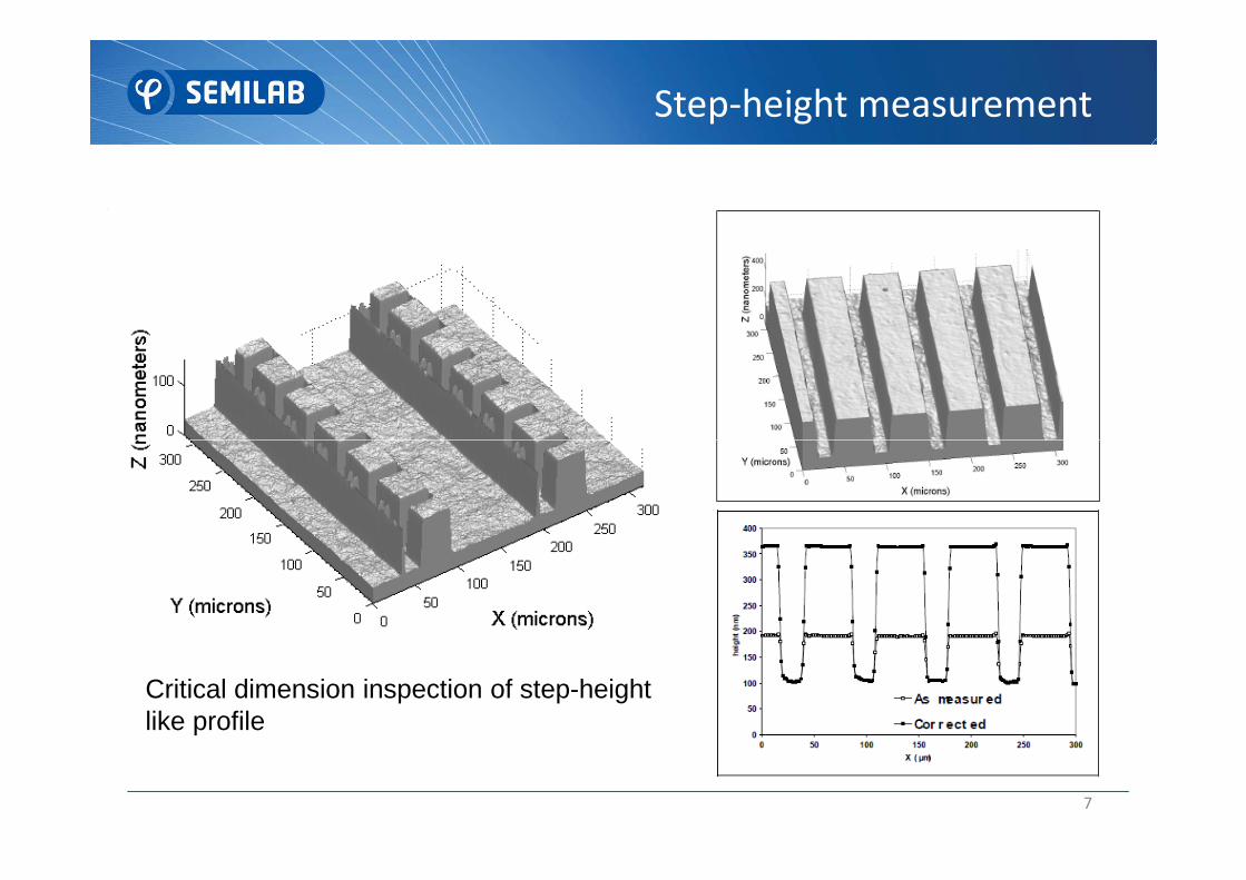
Step-height measurement
7
Critical dimension inspection of step-heightlike profile

Flat Panel Transistor
8
Critical dimension of flat panel transistor

Diamond cut solar cell wafer
1700 nm
9
Solar cell wafer inspection of saw mark, surface roughness and features.0

Metal surface
3000 nm
10
Metal surface inspection of screatches, surface roughness and features.
0

Critical dimension of MEMS device
400 nm
11
0

Optical surface with dust
1000 nm
12
0
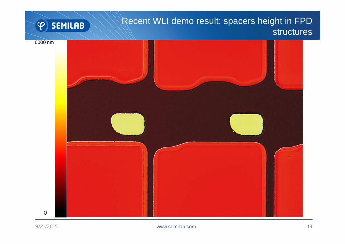
Recent WLI demo result: spacers height in FPD structures
6000 nm
www.semilab.com9/21/2015 13
0

Measurements Positions
Repeatibility measurement
www.semilab.com9/21/2015 14
The Critical dimensions (Top and Bottom) are measured along the yellow axes(nm)

3D view of FPD structures
www.semilab.com 15

Application examplesSurface roughness

935575/4
200 nm
www.semilab.com 17
0

Surface roughness and waviness
200 nm
RMS=4.797 nm
www.semilab.com 18
0
RMS=36.273 nm

Surface roughness and waviness II.
RMS=4.797 nm
www.semilab.com 19
RMS=36.273 nm

9355755/128
250 nm
www.semilab.com 20
0

Surface roughness and waviness
Bandpass
(0.027 to
2.75 um)
www.semilab.com 21
Bandpass
(2.75 to
555 um)

RMS=9.433 nm
www.semilab.com 22
RMS= 27.298 nm

934344/4
250 nm
www.semilab.com 23
0
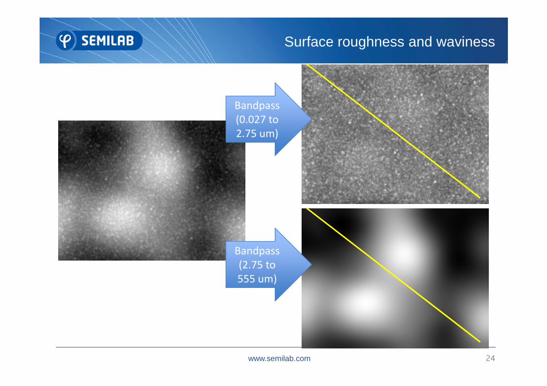
Surface roughness and waviness
Bandpass
(0.027 to
2.75 um)
www.semilab.com 24
Bandpass
(2.75 to
555 um)

RMS=7.762
www.semilab.com 25
RMS= 36.554

934344/128
400 nm
www.semilab.com 26
0

Surface roughness and waviness
Bandpass
(0.027 to
2.75 um)
www.semilab.com 27
Bandpass
(2.75 to
555 um)

RMS=28.122 nm
www.semilab.com 28
RMS= 50.088 nm

• Semilab is capable to deliver state of art 3d surface profiling metrology using white
light interferometry
• Best resolution available : high resolution camera can deliver data up to 2 Megapixels,
in less than 3s aquisition time
Conclusions
www.semilab.com
in less than 3s aquisition time
• Semilab wli technology proved to work for various industrial applications in the flat
panel, solar cell and semiconductor area
• Excellent repeatability is proven to be in the range of few nm-s
29