Wear optimized consumables for copper wire bonding … · Published in: Proceedings of CIPS...
7
Published in: Proceedings of CIPS Nurem Wear optimized consu mass production Michael Brökelmann 1 , Dirk Siepe 1 , Mat 1 Hesse GmbH, Paderborn, D-33100, Ge 2 Infineon Technologies AG, Max-Planc Abstract Copper wire as a bonding material for drawback in heavy copper wire bondi mechanisms and the corresponding fact tested in long-term bonding tests. Optim ing both, an immense improvement in t ter and wire guide are also examined. A is addressed. It is also shown how wear correlates to the actual wear status. The and efficient interconnection technology 1 Introduction In the last few years new technolog power semiconductor devices have been fill the increasing demands of high perf reliability applications, like the growi newable energy and electric vehicles. higher power density and higher junc Besides advanced die attach techniques top side connection also has to be imp cannot be the material of choice anymo ited electrical conductivity and temper stead copper wire as a bonding material because of the superior material proper and thermal conductivity, as well as th bility of copper interconnections, are s than those made with aluminium. Ad wire bonded on copper-metalized die thermo-mechanical mismatch and thus time and reliability of the topside die in [2] Products with copper wire techno available (Figure 1) and increasingl launched in the near future. 2 Copper Wire Bonding Advantages and Chall The major drawback in heavy coppe the low lifetime of the consumables, e tools and cutters. Compared to alu Modulus and yield strength of coppe higher. Because of this, bonding for power are about 2 to 3 times as high com aluminium bonding. In combination w and abrasive properties of the copper cantly reduces the lifetime of the consum Due to the reduced lifetime of the co higher price of copper wire per meter, are currently higher compared to alum 2016 – 9th International Conference on Integrated Pow mberg/Germany, March 8-10, 2016, pp. 211-217 umables for copper wire bondin tthias Hunstig 1 , Karsten Guth 2 , Mark Schnietz 2 ermany ck-Straße 5, D-59581 Warstein, Germany the top side connection of power semiconductors is h ing is the relatively low lifetime of the consumable tors are investigated in this contribution. Different app mized bonding parameters and special tool material ar tool lifetime of a factor of more than 15 was achieved Additionally, the impact of bonding tool wear on differ r can be monitored by machine process data recording ese major advances in heavy copper wire bonding now y. gies for connecting n developed to ful- formance and high ing markets of re- Major trends are ction temperatures. s like sintering, the proved. Aluminium ore, due to its lim- rature stability. In- l is highly desired, rties. The electrical he mechanical sta- significantly higher dditionally, copper es shows reduced increases the life- nterconnection. [1], ology are already gly more will be g lenges er wire bonding is especially bonding uminium, Young’s er are significantly rce and ultrasonic mpared to standard with the hardness wire, this signifi- mables. onsumables and the , the process costs minium. This still prevents the use of copper in p production. In addition, the pro tors have to be designed for the minium as a top side metal on d allow copper wire bonding. Figure 1 20 mil Copper wire b semiconductor module with cop nologies, bottom) State-of-the-art aluminium have a change interval for th 100’000 touchdowns (TDs). Bo by removing the material build cess, and reused several times u lion TDs. The same applicatio typical bonding tool change i 30’000 TDs. With copper wire up which could be removed by wer Electronics Systems, ng in industrial highly desired. One current es. The bonding tool wear proaches to reduce wear are re two of these. Incorporat- d. Wear and lifetime of cut- rent aspects of bond quality g and how a derived signal w make it a robust, reliable place of aluminium in mass oducts and the semiconduc- he use of copper wire. Alu- dies or leadframes does not bonding (top) and power pper wires (Infineon Tech- wire bonding processes he bonding tool of about onding tools can be cleaned d-up occurring in the pro- up to a total of about 1 mil- on with copper wire has a interval of not more than there is no material build- y cleaning, but the bonding
Transcript of Wear optimized consumables for copper wire bonding … · Published in: Proceedings of CIPS...
Published in: Proceedings of CIPS
Nuremberg/Germany,
Wear optimized consumables for copper wire bonding in industrial
mass production
Michael Brökelmann1, Dirk Siepe
1, Matthias Hunstig
1 Hesse GmbH, Paderborn, D-33100, Germany
2 Infineon Technologies AG, Max-Planck
Abstract Copper wire as a bonding material for the top side connection of power semiconductors is highly desired.
drawback in heavy copper wire bondin
mechanisms and the corresponding factors are investigated
tested in long-term bonding tests. Optimized bonding
ing both, an immense improvement in tool lifetime
ter and wire guide are also examined. Additionally, the impact of bonding t
is addressed. It is also shown how wear can be monitored by machine process data recording and how a derived signal
correlates to the actual wear status. These maj
and efficient interconnection technology.
1 Introduction
In the last few years new technologies for connecting
power semiconductor devices have been developed to fu
fill the increasing demands of high performance and high
reliability applications, like the growing markets
newable energy and electric vehicles.
higher power density and higher junction temperatures.
Besides advanced die attach techniques like sintering,
top side connection also has to be improved
cannot be the material of choice anymore,
ited electrical conductivity and temperature stability.
stead copper wire as a bonding material is highly desired
because of the superior material properties
and thermal conductivity, as well as the mechanical st
bility of copper interconnections, are significantly higher
than those made with aluminium. Additionally, copper
wire bonded on copper-metalized dies shows reduced
thermo-mechanical mismatch and thus in
time and reliability of the topside die interconnection.
[2]
Products with copper wire technology are already
available (Figure 1) and increasingly more will be
launched in the near future.
2 Copper Wire Bonding
Advantages and Challenges
The major drawback in heavy copper wire bonding
the low lifetime of the consumables, especially bonding
tools and cutters. Compared to aluminium, Young’s
Modulus and yield strength of copper are significantly
higher. Because of this, bonding force and ultrasonic
power are about 2 to 3 times as high compared to standard
aluminium bonding. In combination with the hardness
and abrasive properties of the copper wire, this signif
cantly reduces the lifetime of the consumables.
Due to the reduced lifetime of the consumables and the
higher price of copper wire per meter, the process costs
are currently higher compared to aluminium. This still
2016 – 9th International Conference on Integrated Power Electronics Systems
Nuremberg/Germany, March 8-10, 2016, pp. 211-217
optimized consumables for copper wire bonding in industrial
, Matthias Hunstig1, Karsten Guth
2, Mark Schnietz
2
33100, Germany
Planck-Straße 5, D-59581 Warstein, Germany
for the top side connection of power semiconductors is highly desired.
drawback in heavy copper wire bonding is the relatively low lifetime of the consumables
mechanisms and the corresponding factors are investigated in this contribution. Different approaches
Optimized bonding parameters and special tool material are two of these.
improvement in tool lifetime of a factor of more than 15 was achieved
ter and wire guide are also examined. Additionally, the impact of bonding tool wear on different aspects of bond quality
is addressed. It is also shown how wear can be monitored by machine process data recording and how a derived signal
correlates to the actual wear status. These major advances in heavy copper wire bonding now
technology.
In the last few years new technologies for connecting
power semiconductor devices have been developed to ful-
fill the increasing demands of high performance and high
reliability applications, like the growing markets of re-
newable energy and electric vehicles. Major trends are
higher power density and higher junction temperatures.
Besides advanced die attach techniques like sintering, the
has to be improved. Aluminium
anymore, due to its lim-
ited electrical conductivity and temperature stability. In-
opper wire as a bonding material is highly desired,
because of the superior material properties. The electrical
onductivity, as well as the mechanical sta-
ity of copper interconnections, are significantly higher
than those made with aluminium. Additionally, copper
metalized dies shows reduced
mechanical mismatch and thus increases the life-
time and reliability of the topside die interconnection. [1],
technology are already
and increasingly more will be
Copper Wire Bonding
hallenges
The major drawback in heavy copper wire bonding is
the low lifetime of the consumables, especially bonding
tools and cutters. Compared to aluminium, Young’s
Modulus and yield strength of copper are significantly
higher. Because of this, bonding force and ultrasonic
compared to standard
aluminium bonding. In combination with the hardness
and abrasive properties of the copper wire, this signifi-
cantly reduces the lifetime of the consumables.
Due to the reduced lifetime of the consumables and the
wire per meter, the process costs
are currently higher compared to aluminium. This still
prevents the use of copper in place of aluminium in mass
production. In addition, the products and the semicondu
tors have to be designed for the use of copper wire. A
minium as a top side metal on dies or leadframes does not
allow copper wire bonding.
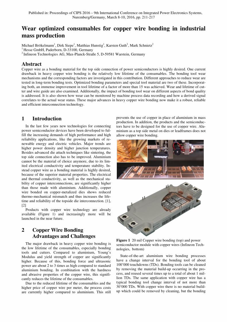
Figure 1 20 mil Copper wire bonding
semiconductor module with copper wires
nologies, bottom)
State-of-the-art aluminium wire bonding
have a change interval for the bonding tool of about
100’000 touchdowns (TDs). Bonding tools can be cleaned
by removing the material build
cess, and reused several times up to a total of
lion TDs. The same application with copper wire has a
typical bonding tool change interval of
30’000 TDs. With copper wire there is no material build
up which could be removed by cleaning
Conference on Integrated Power Electronics Systems,
optimized consumables for copper wire bonding in industrial
for the top side connection of power semiconductors is highly desired. One current
g is the relatively low lifetime of the consumables. The bonding tool wear
ifferent approaches to reduce wear are
ial are two of these. Incorporat-
of a factor of more than 15 was achieved. Wear and lifetime of cut-
ool wear on different aspects of bond quality
is addressed. It is also shown how wear can be monitored by machine process data recording and how a derived signal
now make it a robust, reliable
place of aluminium in mass
production. In addition, the products and the semiconduc-
tors have to be designed for the use of copper wire. Alu-
minium as a top side metal on dies or leadframes does not
20 mil Copper wire bonding (top) and power
semiconductor module with copper wires (Infineon Tech-
art aluminium wire bonding processes
have a change interval for the bonding tool of about
100’000 touchdowns (TDs). Bonding tools can be cleaned
by removing the material build-up occurring in the pro-
up to a total of about 1 mil-
cation with copper wire has a
typical bonding tool change interval of not more than
30’000 TDs. With copper wire there is no material build-
which could be removed by cleaning, but the bonding
Published in: Proceedings of CIPS 2016 – 9th International Conference on Integrated Power Electronics Systems,
Nuremberg/Germany, March 8-10, 2016, pp. 211-217
tool is worn out. The reduced change interval results in
increased machine downtime and more operator support.
Together with the increased bonding tool costs this results
in higher cost per unit which makes copper wire bonding
more cost intensive.
From this state of the art, we can set two targets for tool
and machine suppliers. First, to increase the lifetime of
copper bonding tools by changing material, design and
bonding process parameters and second, to implement a
non-destructive quality sensor to ensure the required in-
terconnection quality and to determine the actual wear
status of the bonding tool.
3 Tool Lifetime Investigation
3.1 Experimental setup
For the lifetime investigations an experimental setup
with ‘typical’ parameters and components for 500 µm (20
mil) copper wire bonding was chosen. The wire used is
PowerCu from Heraeus. Because of the immense amount
of bonds required, ordinary copper plates with a clean and
smooth surface were used for bonding. The experiments
were done on a Hesse BJ939 wire bonder with a back-cut
copper-bondhead, being able to supply bonding forces up
to 4200 cN and ultrasonic power up to 120 watts.
To accelerate the lifetime investigations, single bonds
without looping were made (see Figure 2 and Figure 3).
3.2 Tool wear mechanisms
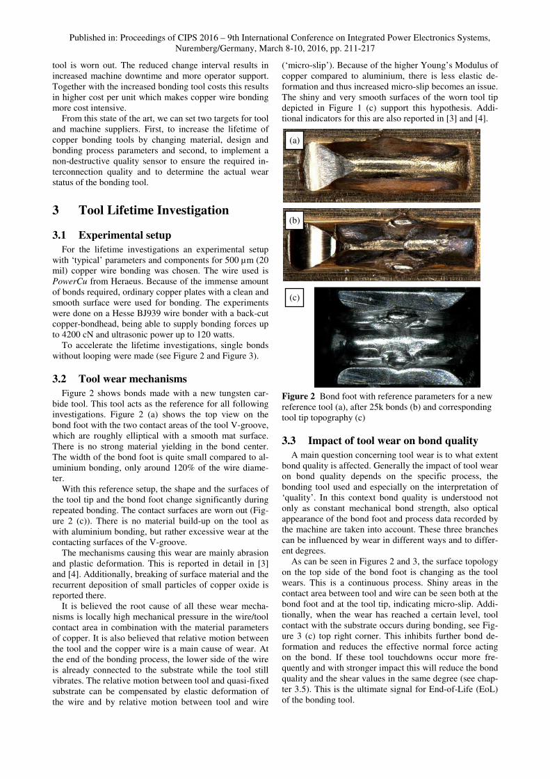
Figure 2 shows bonds made with a new tungsten car-
bide tool. This tool acts as the reference for all following
investigations. Figure 2 (a) shows the top view on the
bond foot with the two contact areas of the tool V-groove,
which are roughly elliptical with a smooth mat surface.
There is no strong material yielding in the bond center.
The width of the bond foot is quite small compared to al-
uminium bonding, only around 120% of the wire diame-
ter.
With this reference setup, the shape and the surfaces of
the tool tip and the bond foot change significantly during
repeated bonding. The contact surfaces are worn out (Fig-
ure 2 (c)). There is no material build-up on the tool as
with aluminium bonding, but rather excessive wear at the
contacting surfaces of the V-groove.
The mechanisms causing this wear are mainly abrasion
and plastic deformation. This is reported in detail in [3]
and [4]. Additionally, breaking of surface material and the
recurrent deposition of small particles of copper oxide is
reported there.
It is believed the root cause of all these wear mecha-
nisms is locally high mechanical pressure in the wire/tool
contact area in combination with the material parameters
of copper. It is also believed that relative motion between
the tool and the copper wire is a main cause of wear. At
the end of the bonding process, the lower side of the wire
is already connected to the substrate while the tool still
vibrates. The relative motion between tool and quasi-fixed
substrate can be compensated by elastic deformation of
the wire and by relative motion between tool and wire
(‘micro-slip’). Because of the higher Young’s Modulus of
copper compared to aluminium, there is less elastic de-
formation and thus increased micro-slip becomes an issue.
The shiny and very smooth surfaces of the worn tool tip
depicted in Figure 1 (c) support this hypothesis. Addi-
tional indicators for this are also reported in [3] and [4].
Figure 2 Bond foot with reference parameters for a new
reference tool (a), after 25k bonds (b) and corresponding
tool tip topography (c)
3.3 Impact of tool wear on bond quality
A main question concerning tool wear is to what extent
bond quality is affected. Generally the impact of tool wear
on bond quality depends on the specific process, the
bonding tool used and especially on the interpretation of
‘quality’. In this context bond quality is understood not
only as constant mechanical bond strength, also optical
appearance of the bond foot and process data recorded by
the machine are taken into account. These three branches
can be influenced by wear in different ways and to differ-
ent degrees.
As can be seen in Figures 2 and 3, the surface topology
on the top side of the bond foot is changing as the tool
wears. This is a continuous process. Shiny areas in the
contact area between tool and wire can be seen both at the
bond foot and at the tool tip, indicating micro-slip. Addi-
tionally, when the wear has reached a certain level, tool
contact with the substrate occurs during bonding, see Fig-
ure 3 (c) top right corner. This inhibits further bond de-
formation and reduces the effective normal force acting
on the bond. If these tool touchdowns occur more fre-
quently and with stronger impact this will reduce the bond
quality and the shear values in the same degree (see chap-
ter 3.5). This is the ultimate signal for End-of-Life (EoL)
of the bonding tool.
(a)
(b)
(c)

Published in: Proceedings of CIPS 2016 – 9th International Conference on Integrated Power Electronics Systems,
Nuremberg/Germany, March 8-10, 2016, pp. 211-217
But until this stadium the observed tool wear does not
directly correlate with the bond strength and the shear
values. The shear values stay constant for many bonds
(see Table 1), despite the ongoing wear. Investigations in
[6] of the shear surfaces (surfaces after shear test) have
shown that even though the contact surfaces at the tool tip
are strongly worn after 100k bonds, the effective contact
area between substrate and wire is almost the same as
with a new tool. Obviously, the normal forces acting on
the wire as well as the ultrasonic coupling between tool
and wire are still sufficient to form a stable interconnec-
tion at this level of wear. Nevertheless, the process will
change with further increasing wear and to some degree,
bond quality will degrade. It should be pointed out that
while the principal wear mechanisms are the same for
bonding on Direct Bonded Copper (DBC) substrates, as
already observed in [3], [4], their specific extent can be
different on DBC than it is on the investigated copper
plates.
3.4 Impact of bonding parameters on wear
The bonding parameters do not only have a big influ-
ence on the bonding itself, they also have a strong impact
on tool wear. The most important parameters are the ul-
trasonic amplitude or power, the (normal) bonding force
and the initial touchdown force [5]. Generally ultrasonic
amplitude and bonding force are varied linearly in some
intervals during bonding. This gives a great multitude of
possible parameter sets and therefore bonding processes.
Figure 3 Bond foot with optimized parameters and new
reference tool (a), after 25k bonds (b) and 100k bonds (c)
As shown in chapter 3.2, with the reference bonding
tool and the reference bonding parameters the wear of the
tool tip progresses quite fast. These parameters were de-
veloped for maximal bonding strength with a high safety
margin, tool wear was not in the focus. It was possible to
find an alternative set of parameters with equivalent bond-
ing performance, but with much less tool wear. The main
reason for this was a reduced bonding time of less than
200 ms instead of more than 300 ms in the reference pa-
rameter set.
Despite the shorter bonding time, this wear-optimized
parameter set showed the same optical and mechanical
quality as the reference parameter sets. Figure 3 depicts
the quality and wear status of the bond foot over time.
The corresponding shear values are part of Table 1 (Tool
A). Comparing the contact surfaces of the bond feet in
Figure 2 (a) and Figure 3 (a) also reveals the reduced mi-
cro-slip with the optimized parameters as the main driver
for tool wear. While the reference process shows quite
pronounced smooth and shiny surfaces in the outer con-
tact area, in case of the wear-optimized process the sur-
faces look more mat and uniform. Even after 25k bonds
the contact surfaces still show not much degrading, at
least in the centre of the contact area. After 100k bonds
also with the optimized parameters increased micro-slip
apparently occurs. Additionally, increased tool touch-
downs indicate tool-EoL in this state of wear. But it can
be pointed out that with optimized bonding parameters the
tool lifetime can be raised by a factor of 4 without loss of
bond quality. This is a big improvement in copper wire
bonding.
3.5 Impact of tool material on wear
The most important factor in tool wear and tool lifetime
is of course the tool tip material itself. If the material can-
not withstand the extreme high static and dynamic stress-
es and strains in heavy copper wire bonding, tool lifetime
will not reach the benchmark level of aluminium bonding
(see chapter 2).
Since decades the standard tool material in heavy (alu-
minium) wire bonding is tungsten carbide. But also ad-
vanced materials for better grip and increased lifetime are
available. Primarily these are so called cermet materials.
Cermet material is a composite of a ceramic base material
in a metallic matrix. Bonding tests with such a cermet
tipped tool (Tool B) have also been conducted, but no
significant improvement in lifetime was found. In [3] it is
reported that for heavy copper wire bonding the wear
mechanisms are basically the same as for reference tung-
sten carbide material, but occur in a different extent.
In lifetime tests a tool with a special wear resistant tip
material (Tool C) showed superior performance and sus-
tainability. These tests were planned to compare the main
tool materials under equal conditions to yield a real
benchmark. Test were repeated – where possible even
with material from different tool suppliers – to get reliable
results. For all tests the optimized parameter set intro-
duced in chapter 3.4 was used. Additionally the condi-
tions specified in chapter 3.1 have been applied.
All relevant information and measures for the examina-
tion of the wear progression have been collected and
evaluated.
(a)
(b)
(c)
Published in: Proceedings of CIPS
Nuremberg/Germany,
Tool A (Tungsten Carbide
Bond
foot
New
tool
Bond
foot
100k
bonds
Bond
foot
500k
bonds
–
Tool
back
side
100k
bonds
Tool
flank
100k
bonds
Tool
flank
500k
bonds –
Shear
values
Table 1 Comparison of tungsten carbide tool, cermet tipped tool and special wear resistant tool
amount of bonds for tool C of up to 500
0
2000
4000
6000
8000
10000
Sh
ea
r fo
rce
[cN
]
# single bonds
mean M
M +/- 3x std. deviation
#15 samples
2016 – 9th International Conference on Integrated Power Electronics Systems
Nuremberg/Germany, March 8-10, 2016, pp. 211-217
Tungsten Carbide) Tool B (Cermet) Tool C
–
–
Comparison of tungsten carbide tool, cermet tipped tool and special wear resistant tool
amount of bonds for tool C of up to 500’000 (different intervals for shear values)
3x std. deviation
0
2000
4000
6000
8000
10000
Sh
ea
r fo
rce
[cN
]
# single bonds
mean M
M +/- 3x std. deviation
#15 samples0
2000
4000
6000
8000
10000
Sh
ea
r fo
rce
[cN
]
Conference on Integrated Power Electronics Systems,
(Special Tip Material)
Comparison of tungsten carbide tool, cermet tipped tool and special wear resistant tool. Note the extended
# single bonds
mean M
M +/- 3x std. deviation
#15 samples
Published in: Proceedings of CIPS 2016 – 9th International Conference on Integrated Power Electronics Systems,
Nuremberg/Germany, March 8-10, 2016, pp. 211-217
Microscope pictures of the bond foot and the tool tip con-
tact area have been made in an interval of at least 10k
bonds. Corresponding shear test values have also been
recorded (Table 1) as well as continuous machine data
from the quality monitoring system (see chapter 4).
The main results are depicted in Table 1. As already
stated in chapter 3.4 the tungsten carbide tool (Tool A)
reached its EoL at 100k bonds. The shear values show a
drop from stable 8000 cN (gf) to 7000 cN at 100k bonds.
The wear has significantly changed the topography of the
bond foot. The flanks are strongly deformed with wavy
structures. The bond foot crest is smaller compared to the
initial state. This is an indication that material has been
worn-out, so that copper wire material can flow deeper
into the V-groove during bonding. The back side view
also shows deep carving of the wire into the tool flank.
This wear out causes tool touchdowns during bonding
starting at 90k bonds. Shiny surface areas on the bond
foot but especially at the tool flanks also indicate micro-
slip and a loss of grip.
The course of wear for the cermet tool (Tool B) is very
similar to the tungsten carbide tool. First tool touchdowns
were noticed at 95k bonds. The shear values stay constant
around 7000 cN. But the optical appearance of bond foot,
tool flanks and tool back side together with the appear-
ance of tool touchdowns and the indication of the ma-
chine data (wear monitor in chapter 4.2) attest that this
cermet tool is very close to its EoL after 100k bonds.
Tool C shows a totally different performance. It was
driven to half a million bonds and still showed very little
wear and very good bonding results. The appearance of
the bond foot almost stayed constant with constantly
formed mat contact surfaces and a constant wide crest. No
carving in the back side view is visible. The tool flanks
only show a minor wear at the contact area. In compari-
son with the tungsten carbide and the cermet tool the sur-
face seems quite rough with a coarse texture. It can be as-
sumed that there is less micro-slip which additionally pre-
vents wear. The shear values did not degrade noticeable
till 500.000 bonds, showing values of about 7000 cN. No
tool touchdowns were observed and the machine data
monitored only small deviations from initial state. The
test was stopped at half a million bonds because of lack of
time and material, but it was repeated with an identical
tool later and identical results were achieved till 500k. It
can be assumed that many more bonds can be made with
this tool untill its EoL will be reached. If 1 million bonds
will be reached, this would be the same amount as can be
reached currently in aluminium bonding when tools are
cleaned several times.
This result is really a breakthrough for heavy copper
wire bonding. If the benchmark lifetime is compared to
the initial lifetime a multiplication factor of more than 15
has been proven and even more is expected.
3.6 Impact of tool tip geometry on wear
To suppress or at least reduce the relative motion be-
tween bonding tool and wire, a modified tool tip geometry
was introduced in [7] and investigated in [3], [4]. Slightly
reduced wear and a reduced process fluctuation were re-
ported, but a significant reduction of the micro-slip could
not be proven. This is in agreement with results of bond-
ing experiments done within this study. Compared to the
reference tool, an increased lifetime of about 30% was
observed. Further studies on geometry optimization are
ongoing and will be reported in the future.
4 Monitoring Tool Wear
To monitor the bonding tool wear and indicate the need
for a tool change, appropriate machine data has to be col-
lected and processed and a ‘wear monitor’ signal has to be
derived.
4.1 Machine data processing
Modern wire bonding machines are able to monitor a
multitude of different process signals in real time such as
ultrasonic current, vertical wire deformation and resonant
frequency during bonding. In this study the wire bonder
was equipped with a process integrated quality control
system (PiQC), providing an additional mechanical ultra-
sonic vibration signal as well as a derived friction-related
signal [8], [9].
The bonding tool wear affects the different physical
machine signals to a different extent. The vertical wire
deformation was found to be especially sensitive to bond-
ing tool wear. As discussed in chapter 3.2, the geometry
of the bonding tool contact area changes due to the ongo-
ing wear. This affects the wire deformation signal.
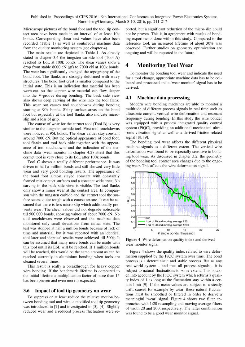
Figure 4 Wire deformation quality index and derived
wear monitor signal
Figure 4 shows the quality index related to wire defor-
mation supplied by the PiQC system over time. The bond
process is a deterministic and stable process. But as any
real world system – and thus all process signals – it is
subject to natural fluctuations to some extent. This is tak-
en into account by the PiQC system which returns a quali-
ty index of 1 as long as the fluctuation stay within a cer-
tain limit [9]. If the mean values are subject to a steady
drift, caused for example by wear, these natural fluctua-
tions must be smoothed or filtered in order to derive a
meaningful ‘wear’ signal. Figure 4 shows two filter ap-
proaches with 1:20 resampling and moving average filters
of width 20 and 200, respectively. The latter combination
was found to be a good wear monitor signal.
0 5 10 15 20 250
0.1
0.2
0.3
0.4
0.5
0.6
0.7
0.8
0.9
1
Qi [
-]
# single bonds [thousand]
raw
1 out of 20 and moving average #20
1 out of 20 and moving average #200
Published in: Proceedings of CIPS
Nuremberg/Germany,
The sensitivity of the overall quality index is
lower than the quality index of the wire deformation, b
cause the other signals included in the overall index are
influenced by wear in minor degree. In cases the wire d
formation is affected by other process deviations in the
sense of ‘disturbances’, the overall quality index could
react more ‘robust’ to tool wear and could be used as an
alternative.
4.2 Online detection of tool end
This approach was tested for different bonding too
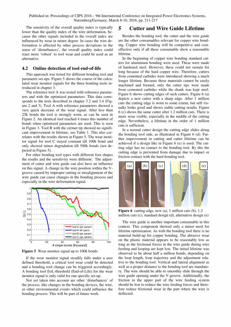
parameter set-ups. Figure 5 shows the course of the cal
lated wear monitor signals for the three
troduced in chapter 3.
The reference tool A was tested with reference param
ters and with the optimized parameters. This data corr
sponds to the tests described in chapter
ure 2 and 3). Tool A with reference parameters showed a
very quick decrease of the wear signal. After less than
25k bonds the tool is strongly worn, as can be seen in
Figure 2. An identical tool reached 4 times this number of
bonds when optimized parameters are used. This is seen
in Figure 3. Tool B with the cermet tip showed no sign
cant improvement in lifetime, see Table 1. This also co
relates with the results shown in Figure 5. The wear mon
tor signal for tool C stayed constant till 100k bond and
only showed minor degradation till 500k bonds (not d
picted in Figure 5).
For other bonding tool types with different foot shapes
the results and the sensitivity were different.
ment of cutter and wire guide can also
on this signal. A change in the wire position within the V
groove caused by improper cutting or misalignment of the
wire guide can cause changes in the bonding process and
especially in the wire deformation signal.
Figure 5 Wear monitor signal up to 100k bonds
If the wear monitor signal steadily falls under a user
defined threshold, a critical tool wear could be detected
and a bonding tool change can be triggered accordingly.
A bonding tool EoL-threshold (End-of-
monitor signal is only valid for one specific set
Not yet taken into account are other ‘disturbances’ of
the process, like changes in the bonding devices, the wire,
or other environmental events which could influence the
bonding process. This will be part of future work.
0 20 40 600
0.1
0.2
0.3
0.4
0.5
0.6
0.7
0.8
0.9
1
# single bonds [thousand]
Qi [
-]
tool A opt. param.
tool A ref. parm.
tool B opt. param.
tool C opt. param.
2016 – 9th International Conference on Integrated Power Electronics Systems
Nuremberg/Germany, March 8-10, 2016, pp. 211-217
The sensitivity of the overall quality index is typically
lower than the quality index of the wire deformation, be-
cause the other signals included in the overall index are
influenced by wear in minor degree. In cases the wire de-
formation is affected by other process deviations in the
ces’, the overall quality index could
and could be used as an
Online detection of tool end-of-life
This approach was tested for different bonding tool and
shows the course of the calcu-
three bonding tools in-
ool A was tested with reference parame-
ters and with the optimized parameters. This data corre-
sponds to the tests described in chapter 3.2 and 3.4 (Fig-
ure 2 and 3). Tool A with reference parameters showed a
the wear signal. After less than
25k bonds the tool is strongly worn, as can be seen in
Figure 2. An identical tool reached 4 times this number of
bonds when optimized parameters are used. This is seen
in Figure 3. Tool B with the cermet tip showed no signifi-
cant improvement in lifetime, see Table 1. This also cor-
relates with the results shown in Figure 5. The wear moni-
tor signal for tool C stayed constant till 100k bond and
only showed minor degradation till 500k bonds (not de-
bonding tool types with different foot shapes
the results and the sensitivity were different. The adjust-
also have an influence
. A change in the wire position within the V-
or misalignment of the
wire guide can cause changes in the bonding process and
especially in the wire deformation signal.
Wear monitor signal up to 100k bonds
If the wear monitor signal steadily falls under a user
tool wear could be detected
and a bonding tool change can be triggered accordingly.
-Life) for the wear
monitor signal is only valid for one specific set-up.
ot yet taken into account are other ‘disturbances’ of
cess, like changes in the bonding devices, the wire,
or other environmental events which could influence the
This will be part of future work.
5 Cutter and Wire
Besides the bonding tool, the cutter and the wire guide
are the other consumables relevant for copper wire bon
ing. Copper wire bonding will be competitive and cost
effective only if all these consumable show a reasonable
lifetime.
In the beginning of copper wire bonding standard cu
ters for aluminium bonding were used
of hardened steel. However, these could not sustain for
long because of the hard copper wire. Therefore, cutters
from cemented carbides were introduced showing a much
longer lifetime. Because these materials cannot be easily
machined and formed, only the cutter tips were made
from cemented carbides while the shank was kept steel.
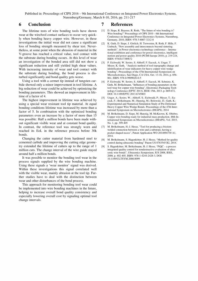
Figure 6 shows cutting edges of such cutters.
depicts a new cutter with a sharp edge. After 1 million
cuts the cutting edge is worn to some extent, b
ually looks good and shows stable cutting results.
6 (c) shows the same cutter after 1.2 million cuts. There is
more wear visible, especially in the middle of the cutting
edge. Nevertheless, a lifetime in the order of 1 million
cuts is sufficient.
In a normal cutter design the cutting edge slides along
the bonding tool side, as illustrated in Figure 6 (d). Fu
ther improvement in cutting and cutter lifetime can be
achieved if a design like in Figure 6 (e) is used. The cu
ting edge has no contact to the bonding tool. By this the
cutting edge is prevented from damage due to impact or
friction contact with the hard bonding tool.
Figure 6 cutting edge, new (a), 1 mi
million cuts (c), standard design
The wire guide is another important consumable in this
context. This component showed only a minor need for
lifetime optimization. As with the bonding tool there is no
material build-up for copper bonding. The abrasive wear
on the plastic material appears to be reasonably low as
long as the frictional forces in the wire guide during wire
feeding and looping are kept low. The initial lifetime was
observed to be about half a million bonds, depending o
the loop length, loop trajectory and the adjustment rel
tive to the bonding tool. Vertical and lateral alignment as
well as a proper distance to the bonding tool are mandat
ry. The wire should be able to smoothly slide through the
wire guide opening under the V
friction in the upper part of the wire feeding system
should be low to reduce the wire feeding forces and ther
fore reduce frictional wear in the part where the wire
deflected.
80 100
# single bonds [thousand]
tool A opt. param.
tool A ref. parm.
tool B opt. param.
tool C opt. param.
(c) (a) (b)
Conference on Integrated Power Electronics Systems,
ire Guide Lifetime
Besides the bonding tool, the cutter and the wire guide
other consumables relevant for copper wire bond-
ing. Copper wire bonding will be competitive and cost-
effective only if all these consumable show a reasonable
In the beginning of copper wire bonding standard cut-
ters for aluminium bonding were used. These were made
of hardened steel. However, these could not sustain for
long because of the hard copper wire. Therefore, cutters
from cemented carbides were introduced showing a much
longer lifetime. Because these materials cannot be easily
formed, only the cutter tips were made
from cemented carbides while the shank was kept steel.
shows cutting edges of such cutters. Figure 6 (a)
depicts a new cutter with a sharp edge. After 1 million
cuts the cutting edge is worn to some extent, but still vis-
ually looks good and shows stable cutting results. Figure
(c) shows the same cutter after 1.2 million cuts. There is
more wear visible, especially in the middle of the cutting
edge. Nevertheless, a lifetime in the order of 1 million
In a normal cutter design the cutting edge slides along
the bonding tool side, as illustrated in Figure 6 (d). Fur-
ther improvement in cutting and cutter lifetime can be
achieved if a design like in Figure 6 (e) is used. The cut-
ontact to the bonding tool. By this the
cutting edge is prevented from damage due to impact or
friction contact with the hard bonding tool.
cutting edge, new (a), 1 million cuts (b), 1.2
design (d), alternative design (e)
The wire guide is another important consumable in this
context. This component showed only a minor need for
lifetime optimization. As with the bonding tool there is no
bonding. The abrasive wear
on the plastic material appears to be reasonably low as
long as the frictional forces in the wire guide during wire
feeding and looping are kept low. The initial lifetime was
observed to be about half a million bonds, depending on
the loop length, loop trajectory and the adjustment rela-
tive to the bonding tool. Vertical and lateral alignment as
well as a proper distance to the bonding tool are mandato-
ry. The wire should be able to smoothly slide through the
r the V-groove. Additionally, the
friction in the upper part of the wire feeding system
should be low to reduce the wire feeding forces and there-
fore reduce frictional wear in the part where the wire is
(d) (e)
Published in: Proceedings of CIPS 2016 – 9th International Conference on Integrated Power Electronics Systems,
Nuremberg/Germany, March 8-10, 2016, pp. 211-217
6 Conclusion
The lifetime tests of wire bonding tools have shown
wear at the wire/tool contact surfaces to occur very quick-
ly when bonding heavy copper wire. However, in these
investigations the initial wear did not cause a significant
loss of bonding strength measured by shear test. Never-
theless, at some point when the abrasion of material in the
V-groove has reached a critical value, tool contact with
the substrate during bonding occurs. At this level of wear
an investigation of the bonded area still did not show a
significant reduction and still yielded high shear values.
With increasing intensity of wear and tool contact with
the substrate during bonding, the bond process is dis-
turbed significantly and bond quality gets worse.
Using a tool with a cermet tip instead of tungsten car-
bide showed only a minor improvement in tool lifetime. A
big reduction of wear could be achieved by optimizing the
bonding parameters. This showed an improvement in life-
time of a factor of 4.
The highest improvement in lifetime was achieved by
using a special wear resistant tool tip material. At equal
bonding conditions lifetime was increased by more than a
factor of 5. In combination with the optimized bonding
parameters even an increase by a factor of more than 15
was possible: Half a million bonds have been made with-
out significant visible wear and at constant bond quality.
In contrast, the reference tool was strongly worn and
reached its EoL in the reference process before 30k
bonds.
Changing the cutter material from hardened steel to
cemented carbide and improving the cutting edge geome-
try extended the lifetime of cutters up to the range of 1
million cuts. The change interval of the wire guide stayed
around half a million bonds.
It was possible to monitor the bonding tool wear in the
process signals supplied by the wire bonding machine.
Using these signals a ‘wear monitor’ signal was derived.
Within these investigations this signal correlated well
with the visible wear, mainly abrasion at the tool tip. Fur-
ther studies have to deal with the distinction between
wear and other disturbances of the bond process.
This approach for monitoring bonding tool wear could
be implemented into wire bonding machines in the future,
helping to increase overall bond quality consistency and
especially lowering overall cost by signaling optimal tool
change intervals.
7 References
[1] D. Siepe, R. Bayerer, R. Roth, “The future of wire bonding is?
Wire bonding!” Proceedings of CIPS 2010 – 6th International
Conference on Integrated Power Electronics Systems, Nuremberg,
Germany, 2010, ISBN: 978-3-8007-3212-8
[2] K. Guth, D. Siepe, J. Görlich, H. Torwesten, R. Roth, F. Hille, F.
Umbach, “New assembly and interconnects beyond sintering
methods”, in Power electronics technology conference – Interna-
tional exhibition and conference for power electronics, intelligent
motion and power quality 2010 (PCIM Europe 2010), p. 219-224,
ISBN: 9781617389672
[3] P. Eichwald, W. Sextro, S. Althoff, F. Eacock, A. Unger, T.
Meyer, K. Guth, “Analysis method of tool topography change and
identification of wear indicators for heavy copper wire wedge
bonding”, Proceedings of the 47th International Symposium on
Microelectronics, San Diego, CA USA, Oct. 13-16, 2014, p. 856-
861, ISBN: 978-0-9909028-0-5
[4] P. Eichwald, W. Sextro, S. Althoff, F. Eacock, M. Schnietz, K.
Guth, M. Brökelmann, “Influences of bonding parameters on the
tool wear for copper wire bonding”, Electronics Packaging Tech-
nology Conference (EPTC 2013), IEEE 15th, 2013, p. 669-672,
DOI: 10.1109/EPTC.2013.6745803
[5] Unger, A.; Sextro, W.; Althoff, S.; Eichwald, P.; Meyer, T.; Ea-
cock, F.; Brökelmann, M.; Hunstig, M.; Bolowski, D.; Guth, K.:
Experimental and Numerical Simulation Study of Pre-Deformed
Heavy Copper Wire Wedge Bonds. Proceedings of the 47th Inter-
national Symposium on Microelectronics (IMAPS), 2014
[6] M. Brökelmann, D. Siepe, M. Hunstig, M. McKeown, K. Oftebro,
Copper wire bonding ready for industrial mass production. 48th In-
ternational Symposium on Microelectronics (IMAPS), Vol. 2015,
No. 1, pp. 399-405
[7] M. Brökelmann, H.-J. Hesse, “Tool for producing a friction-
welded connection between a wire and a substrate, having a
pocket-shaped recess”, Patent Application WO 2014094730 A1,
2014.
[8] M. Brökelmann, S. Hagenkötter, H.-J. Hesse, “Method for quality
control during ultrasonic bonding” Patent US 8783545 B2, 2014.
[9] S. Hagenkötter, M. Brökelmann, H.-J. Hesse, “PiQC – a process
integrated quality control for nondestructive evaluation of ultra-
sonic wire bonds”, Ultrasonics Symposium, IUS 2008, IEEE,
2008, p. 402-405, ISBN: 978-1-4244-2428-3, DOI:
10.1109/ULTSYM.2008.0099