Functionalized Graphene and Graphene Oxide: Materials Synthesis
Copyright (c) 2013 IEEE. Personal use is permitted. For any other purposes, permission must be obtained from the IEEE by emailing [email protected].
This article has been accepted for publication in a future issue of this journal, but has not been fully edited. Content may change prior to final publication.
> REPLACE THIS LINE WITH YOUR PAPER IDENTIFICATION NUMBER (DOUBLE-CLICK HERE TO EDIT) <
1
Abstract—An overview is provided of waveguide-coupled
graphene optoelectronics. A review of the optical properties of
graphene is first provided and a motivation for waveguide-
coupled graphene optoelectronics is given. This motivation is
largely based upon the increased interaction length that can be
achieved using such geometries. A derivation of the optical
absorption for graphene interacting with a guided waveguide
mode wave is provided. Device concepts for waveguide-coupled
graphene optoelectronic devices, including optical modulators,
photodetectors, and polarizers operating in the near- and mid-
infrared regime are then described. This discussion provides a
specific emphasis on the effect of disorder on the expected
performance and energy consumption of graphene-based optical
modulators. Finally, an outlook for future areas of exploration is
given.
Index Terms—Waveguides, Optical Communication,
Nanotechnology
I. INTRODUCTION
A. Graphene background and optical properties
HE unique and extraordinary properties of graphene
have led to consideration of this two-dimensional (2D)
allotrope of carbon for a wide range of device applications
[1-5]. Among its exceptional properties are high mobility [6],
thermal conductivity [7], and mechanical strength [8]; a
gapless linear dispersion relation [9]; and symmetric
ambipolar conductivity [2]. However, perhaps some of the
most interesting properties of graphene are related to its
optical characteristics. For instance, graphene is an ultra-
wideband absorber [10], which is a direct result of its gaplass
band structure; has tunable inter-band absorption [11] as a
well as saturable absorption [12] at high power levels, both
consequences of the low density of states in graphene; and
extremely-high and tunable absorption of terahertz radiation
[13], a consequence of the high dc conductivity and variable
density of states. While the original studies on graphene were
performed on small (e.g. ~ 20 x 20 m2) flakes created by
mechanical exfoliation, the pioneering work in [14]
demonstrated that large sheets of single and multi-layer
graphene can be synthesized readily on metal substrates.
Metal-synthesized graphene can then be transferred onto
arbitrary substrates, allowing wafer-scale processing, thereby
Submited on May 13, 2013. This work was supported in part by the NSF
under Grant No. ECCS-1124831, the AFOSR under Award No. FA9550-12-1-0338, and the University of Minnesota College of Science and Engineering.
S. J. Koester and M. Li are with the University of Minnesota-Twin Cities,
200 Union St. SE, Minneapolis, MN 55455, USA. (e-mails: [email protected] , [email protected]).
making practical device applications within reach. Among the
potential optoelectronic device applications of graphene
include optical modulators [15-17], photodetectors [18,19],
polarization controllers [20] and ultrafast pulsed lasers
[12,21].
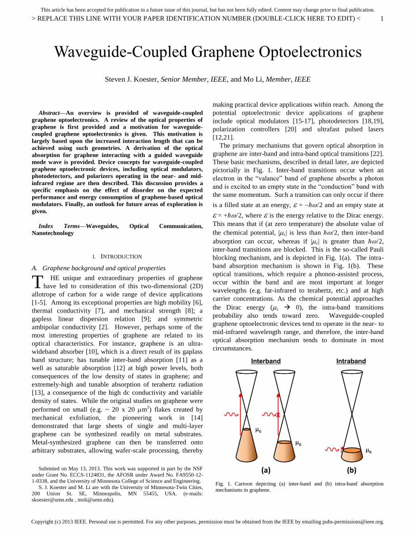
The primary mechanisms that govern optical absorption in
graphene are inter-band and intra-band optical transitions [22].
These basic mechanisms, described in detail later, are depicted
pictorially in Fig. 1. Inter-band transitions occur when an
electron in the “valance” band of graphene absorbs a photon
and is excited to an empty state in the “conduction” band with
the same momentum. Such a transition can only occur if there
is a filled state at an energy, = ħ / 2 and an empty state at
= +ħ / 2, where is the energy relative to the Dirac energy.
This means that if (at zero temperature) the absolute value of
the chemical potential, |c| is less than ħ / 2, then inter-band
absorption can occur, whereas if |c| is greater than ħ / 2,
inter-band transitions are blocked. This is the so-called Pauli
blocking mechanism, and is depicted in Fig. 1(a). The intra-
band absorption mechanism is shown in Fig. 1(b). These
optical transitions, which require a phonon-assisted process,
occur within the band and are most important at longer
wavelengths (e.g. far-infrared to terahertz, etc.) and at high
carrier concentrations. As the chemical potential approaches
the Dirac energy (c 0), the intra-band transitions
probability also tends toward zero. Waveguide-coupled
graphene optoelectronic devices tend to operate in the near- to
mid-infrared wavelength range, and therefore, the inter-band
optical absorption mechanism tends to dominate in most
circumstances.
Waveguide-Coupled Graphene Optoelectronics
Steven J. Koester, Senior Member, IEEE, and Mo Li, Member, IEEE
T
Fig. 1. Cartoon depicting (a) inter-band and (b) intra-band absorption mechanisms in graphene.
Copyright (c) 2013 IEEE. Personal use is permitted. For any other purposes, permission must be obtained from the IEEE by emailing [email protected].
This article has been accepted for publication in a future issue of this journal, but has not been fully edited. Content may change prior to final publication.
> REPLACE THIS LINE WITH YOUR PAPER IDENTIFICATION NUMBER (DOUBLE-CLICK HERE TO EDIT) <
2
In the remainder of this paper we describe how the optical
properties of graphene can be utilized to realize practical
optoelectronic devices. We first describe the detailed optical
properties of graphene and motivate the reason for integration
of graphene with planar photonic wave-guides. Next, we
describe the results of optical absorption measurements of
graphene on Si waveguides that confirm the theoretical
prediction that complete optical absorption can be obtained in
these structures. We next describe the device applications of
graphene-on-waveguide structures, and specifically, review
the status in the field on waveguide-coupled optical
modulators, photodetectors and polarizers. Finally, we
describe future trends and opportunities for graphene-based
waveguide-coupled optoelectronic devices.
II. MOTIVATION FOR WAVEGUIDE COUPLING
Planar photonic waveguides, as well as other photonic
elements including photonic band gap structures and various
types of optical resonators and cavities, are building blocks of
photonic integrated circuits (PIC) and optoelectronic systems.
The integrated circuits for light can guide and route optical
signals on a chip to leverage the unparalleled bandwidth
available in the optical spectrum for communications. In
particular, utilizing silicon’s high index of refraction and
transparency in the important near-infrared band for
telecommunication, silicon photonics promises to integrate
PIC with CMOS circuitry, leading to large scale integrated
(LSI) optoelectronic systems for optical interconnections,
chip-to-chip and intra-chip, and for telecommunication and
optical signal processing applications [23]. Silicon, as an
indirect band-gap semiconductor and centrosymmetric crystal,
however, lacks many important properties that are critical for
active optoelectronics functionalities. Other silicon compatible
materials including silicon nitride (SiN) and silicon oxynitride
(SiON) also can only be used as passive optical materials. To
achieve infrared light emission and photodetection with high
efficiency, the only viable approaches are hybrid integration of
active optoelectronic materials, such as III-V compound
semiconductors and germanium, onto the passive silicon
photonic platform [24,25]. Adding new materials to silicon
photonics allows the best properties of different materials to
be fully exploited in highly integrated, multi-functional
optoelectronic systems.
The 2D structure of graphene and the planar configuration
of silicon photonics are inherently compatible with each other.
Coplanar integration can be readily achieved by transferring
and laminating graphene on top of silicon photonic substrates,
which can be planarized with cladding materials. Such
integration, on one hand, allows graphene’s novel
optoelectronic properties to be effectively utilized in photonic
devices. On the other hand, silicon photonic circuits can
provide a versatile platform to investigate and characterize the
fundamental optical properties of graphene. Although
conventional free-space optical measurement systems have
been instrumental in investigating these properties, practical
application requires graphene to be integrated with existing
photonic technology. Furthermore, coplanar integration
eliminates the restriction of the interaction length between
optical field and graphene, which is limited to the thickness of
graphene (3.3 Å per monolayer) for normal-incident light.
With sufficient length of interaction, graphene induced
optoelectronic effects can become strong and graphene’s
optical properties can be more accurately measured.
Specifically, using graphene integrated on a silicon photonic
waveguide, electrically tunable optical absorption has be
achieved and exploited to create an electro-absorptive optical
modulator [26]. Also, it is well known that graphene has a
universal fractional optical absorption of 2.3% per monolayer
over a wideband of optical frequency for normal incidence,
due to the linear band structure. Converted to absorption
coefficient using graphene’s thickness of 3.3 Å, this
absorption corresponds to an extremely large value of 70.5
m-1
(or 306 dB/m). But with 97.7% transmission through
such a thin film of one atomic layer, graphene is virtually
transparent. When used for photodetection, this low absolute
absorption diminishes the external quantum efficiency of a
graphene photodetector, even though internal efficiency can
be very high [18]. Coplanar integration with a waveguide is an
obvious solution to this problem, and both theoretical and
experiments results on these structures will be described.
III. WAVEGUIDE-COUPLED GRAPHENE OPTICAL DEVICES
A. Optical properties of graphene on waveguides
When graphene is laminated on top of a photonic
waveguide, its coupling with the wave-guide mode induces
optical absorption and dispersion, which can be characterized
by the real and imaginary parts of graphene’s dynamic
conductivity (), respectively. Both inter-band and intra-
band transitions in graphene are responsible for the
conductivity and their relative contributions depend on the
optical frequency, , and the chemical potential, . The total
2D conductivity is complex and can be expressed as
= intra + inter = + i. To relate this 2D conductivity to
the volume permittivity, it is suggested to divide the 2D
conductivity by the thickness of graphene, , as
= 0 + i/ = (0 /) + i/ in the calculation and
then take the limit of 0 [27]. Because of its purely 2D
nature, however, care must be given not to treat graphene
simply as a thin sheet of isotropic material in calculations and
simulation.
Using the Kubo formula [22], the intra-band and inter-band
conductivity of graphene are given by
2
intra 22ln 1
2c Bk TcB
B
e k Ti e
i k T
, (1)
and
2
inter 2 22 0
2
2 4
d die i f fd
i
, (2)
Copyright (c) 2013 IEEE. Personal use is permitted. For any other purposes, permission must be obtained from the IEEE by emailing [email protected].
This article has been accepted for publication in a future issue of this journal, but has not been fully edited. Content may change prior to final publication.
> REPLACE THIS LINE WITH YOUR PAPER IDENTIFICATION NUMBER (DOUBLE-CLICK HERE TO EDIT) <
3
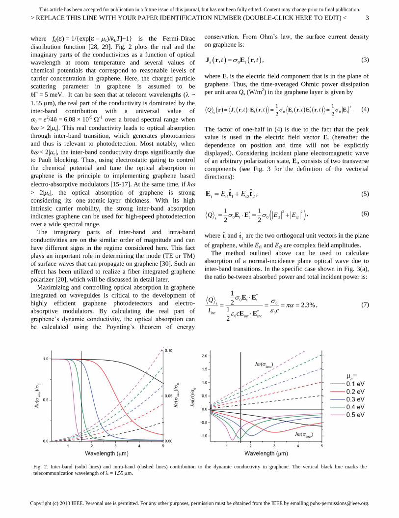
where fd() = 1/{exp[ c)/kBT]+1} is the Fermi-Dirac
distribution function [28, 29]. Fig. 2 plots the real and the
imaginary parts of the conductivities as a function of optical
wavelength at room temperature and several values of
chemical potentials that correspond to reasonable levels of
carrier concentration in graphene. Here, the charged particle
scattering parameter in graphene is assumed to be
ħ = 5 meV. It can be seen that at telecom wavelengths ( ~
1.55 m), the real part of the conductivity is dominated by the
inter-band contribution with a universal value of
0 = e2/4ħ = 6.08 × 10
-5
-1 over a broad spectral range when
ħ > 2|c|. This real conductivity leads to optical absorption
through inter-band transition, which generates photocarriers
and thus is relevant to photodetection. Most notably, when
ħ < 2|c|, the inter-band conductivity drops significantly due
to Pauli blocking. Thus, using electrostatic gating to control
the chemical potential and tune the optical absorption in
graphene is the principle to implementing graphene based
electro-absorptive modulators [15-17]. At the same time, if ħ
> 2|c|, the optical absorption of graphene is strong
considering its one-atomic-layer thickness. With its high
intrinsic carrier mobility, the strong inter-band absorption
indicates graphene can be used for high-speed photodetection
over a wide spectral range.
The imaginary parts of inter-band and intra-band
conductivities are on the similar order of magnitude and can
have different signs in the regime considered here. This fact
plays an important role in determining the mode (TE or TM)
of surface waves that can propagate on graphene [30]. Such an
effect has been utilized to realize a fiber integrated graphene
polarizer [20], which will be discussed in detail later.
Maximizing and controlling optical absorption in graphene
integrated on waveguides is critical to the development of
highly efficient graphene photodetectors and electro-
absorptive modulators. By calculating the real part of
graphene’s dynamic conductivity, the optical absorption can
be calculated using the Poynting’s theorem of energy
conservation. From Ohm’s law, the surface current density
on graphene is:
s 0 t, ,t tJ r E r , (3)
where Et is the electric field component that is in the plane of
graphene. Thus, the time-averaged Ohmic power dissipation
per unit area Qs (W/m2) in the graphene layer is given by
2*
s t 0 t t 0 ts
1 1, , , ,
2 2Q t t t t r J r E r E r E r E . (4)
The factor of one-half in (4) is due to the fact that the peak
value is used in the electric field vector Et (hereafter the
dependence on position and time will not be explicitly
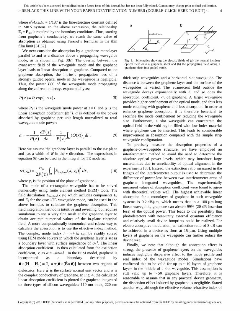
displayed). Considering incident plane electromagnetic wave
of an arbitrary polarization state, Et, consists of two transverse
components (see Fig. 3 for the definition of the vectorial
directions):
t t1 1 t2 2ˆ ˆE E E t t , (5)
2 2*
0 t t 0 t1 t2s
1 1
2 2Q E E E E , (6)
where 1t̂ and
2t̂ are the two orthogonal unit vectors in the plane
of graphene, while Et1 and Et2 are complex field amplitudes.
The method outlined above can be used to calculate
absorption of a normal-incidence plane optical wave due to
inter-band transitions. In the specific case shown in Fig. 3(a),
the ratio be-tween absorbed power and total incident power is:
*
0 t ts 0
*inc 00 inc inc
1
2 2.3%1
2
Q
I cc
E E
E E
, (7)
Fig. 2. Inter-band (solid lines) and intra-band (dashed lines) contribution to the dynamic conductivity in graphene. The vertical black line marks the
telecommunication wavelength of = 1.55 m.
Copyright (c) 2013 IEEE. Personal use is permitted. For any other purposes, permission must be obtained from the IEEE by emailing [email protected].
This article has been accepted for publication in a future issue of this journal, but has not been fully edited. Content may change prior to final publication.
> REPLACE THIS LINE WITH YOUR PAPER IDENTIFICATION NUMBER (DOUBLE-CLICK HERE TO EDIT) <
4
where e2/40ħc = 1/137 is the fine-structure constant defined
in MKS system. In the above expression, the relationship
Et = Einc is required by the boundary conditions. Thus, starting
from graphene’s conductivity, we reach the same value of
absorption as obtained using Fresnel’s formulas in the thin
film limit [31,32].
We next consider the absorption by a graphene monolayer
parallel to and at a distance above a propagating waveguide
mode, as is shown in Fig. 3(b). The overlap between the
evanescent field of the waveguide mode and the graphene
layer leads to linear absorption in graphene. Compared to the
graphene absorption, the intrinsic propagation loss of a
strongly guided optical mode in the waveguide is negligible.
Thus, the power P(z) of the waveguide mode propagating
along the z direction decays exponentially as:
0 expP z P z , (8)
where P0 is the waveguide mode power at z = 0 and is the
linear absorption coefficient (m-1
). is defined as the power
absorbed by graphene per unit length normalized to total
waveguide mode power:
s
1 1( )
W
dP zQ x dl
P z dz P z . (9)
Here we assume the graphene layer is parallel to the x-z plane
and has a width of W in the x direction. The expressions in
equation (6) can be used in the integral for TE mode as:
20
0 in-plane 0( ) ( , )2 W
y E x y dxP z
, (10)
where y0 is the position of the plane of graphene.
The mode of a rectangular waveguide has to be solved
numerically using finite element method (FEM) tools. The
field distribution Ein-plane(x, y0) which includes components Ex
and Ez for the quasi-TE waveguide mode, can be used in the
above formulas to calculate the graphene absorption. This
field integration method is intuitive and revealing, but requires
simulation to use a very fine mesh at the graphene layer to
obtain accurate numerical values of the in-plane electrical
field. A more computationally economical and robust way to
calculate the absorption is to use the effective index method.
The complex mode index ñ = n + i can be readily solved
using FEM mode solvers in which the graphene layer is set as
a boundary layer with surface impedance of 0-1
. The linear
absorption coefficient is then calculated from the extinction
coefficient, , as = 4/. In the FEM model, graphene is
incorporated as a boundary described by
)]nEnJHHn ˆˆ(ˆ[)(ˆ21 s
between two regions of
dielectrics. Here n̂ is the surface normal unit vector and is
the complex conductivity of graphene. In Fig. 4, the calculated
linear absorption coefficient is plotted for graphene integrated
on three types of silicon waveguides: 110 nm thick, 220 nm
thick strip waveguides and a horizontal slot waveguide. The
distance h between the graphene layer and the surface of the
waveguides is varied. The evanescent field outside the
waveguide decays exponentially with h, and so does the
absorption coefficient, , of graphene. A larger waveguide
provides higher confinement of the optical mode, and thus less
mode coupling with graphene and less absorption. In order to
enhance graphene absorption, it is therefore beneficial to
sacrifice the mode confinement by reducing the waveguide
size. Furthermore, a slot waveguide can concentrate the
optical field in the void region filled with low index material
where graphene can be inserted. This leads to considerable
improvement in absorption compared with the simple strip
waveguide configuration.
To precisely measure the absorption properties of a
graphene-on-waveguide structure, we have employed an
interferometric method to avoid the need to determine the
absolute optical power levels, which may introduce large
uncertainties due to unreliability of optical alignment in the
experiments [33]. Instead, the extinction ratio measured in the
fringes of the interferometer output is used to determine the
difference of power loss between two interferometer arms of
graphene integrated waveguides. The experimentally
measured values of absorption coefficient were found to agree
with theoretical values well. The highest achievable linear
absorption for a monolayer of graphene in such waveguide
systems is 0.2 dB/m, which means that in a 100-m-long
linear waveguide, graphene can absorb 99% (20 dB insertion
loss) of the optical power. This leads to the possibility that
photodetectors with near-unity external quantum efficiency
and relatively small device footprints could be realized. For
electro-absorptive modulation, an extinction ratio of 3 dB can
be achieved in a device as short at 15 m. Using multiple
layers of graphene on the waveguide can further reduce the
device size.
Finally, we note that although the absorption effect is
strong, the presence of graphene layers on the waveguides
induces negligible dispersive effect to the mode profile and
real index of the waveguide modes. Simulations have
confirmed this to be valid for up to ~ 10 layers of graphene
layers in the middle of a slot waveguide. This assumption is
still valid up to ~ 50 graphene layers. Therefore, it is
reasonable to assume that in any practical device geometry,
the dispersion effect induced by graphene is negligible. Stated
another way, although the effective volume refractive index of
Fig. 3. Schematics showing the electric fields of (a) the normal incident optical field onto a graphene sheet and (b) the propagating field along a
graphene sheet in a guided mode.
Copyright (c) 2013 IEEE. Personal use is permitted. For any other purposes, permission must be obtained from the IEEE by emailing [email protected].
This article has been accepted for publication in a future issue of this journal, but has not been fully edited. Content may change prior to final publication.
> REPLACE THIS LINE WITH YOUR PAPER IDENTIFICATION NUMBER (DOUBLE-CLICK HERE TO EDIT) <
5
graphene can be high: reff
~ 0/0 ~ 17, due to the atomic
thickness of graphene, the aggregate effect is too small to
disturb a well-guided optical mode in the waveguide
significantly. Surface modes, however, can exist on graphene
and can have significant effects on the polarization states of
the optical mode, which will be discussed in the latter section.
B. Optical modulators
Electro-absorption optical modulators are perhaps the most
compelling and obvious optoelectronic application of
graphene due to the tunable optical absorption that can be
achieved in graphene. Furthermore, as described above,
waveguide geometries are particularly well suited for optical
modulators, due to the fact that nearly complete optical
absorption can be achieved in a graphene-on-waveguide
geometry. However, design of waveguide-coupled graphene
modulators brings about significant challenges, particularly
regarding how to gate graphene without incurring significant
optical losses. These challenges are different than those
incurred using Si optical modulators. In Si, electro-optic
effects are relatively weak, and therefore modulation is
achieved using plasma dispersion effects, where injected
electrons and holes induce slight changes in the Si refractive
index [34]. By utilizing a Mach-Zehnder or ring resonator
design, a tunable phase shift can be induced thus leading to
tunable destructive or constructive interference that creates the
optical modulation signal [35]. Si/SiGe optical modulators
have also been proposed using either the Franz-Keldish effect
or the quantum-confined stark effect, which increases the
electro-optic effects and thus allows more compact modulator
designs. In all of these structures, the electrical contact region
is distinct from the optically active region of the device.
However, in graphene-based optical modulators, graphene
serves the dual role of both electrode and optically active
material. Given this relatively unique mechanism for action,
novel designs are needed for realizing optimized optical
modulators.
The first experimental results on graphene-on-waveguide
optical modulators were reported by Liu, et al. [17]. In this
device structure, a graphene optical modulator is created by
transferring graphene above a silicon waveguide and then
gating the graphene through the waveguide itself. Gating
action is achieved by making a separate contact to the silicon
waveguide through a thin, heavily-doped Si region adjacent to
the waveguide. The basic principle of this device operation
was established and modulators operating at 3.5 V with
extinction ratio (ER) and bandwidth (BW) of ~ 3 dB and
1.2 GHz, respectively, were demonstrated. While this was the
first demonstration of a waveguide-coupled graphene-based
modulator, the design utilized in that work has several
shortcomings. First of all, the device requires electrical
contact to be made through the silicon waveguide itself, and
therefore, the Si needs to be doped and contacted using a thin,
heavily-doped extension region. The high doping can
introduce free carrier absorption in the Si waveguide, leading
to increased insertion loss. It also introduces an extra level of
process complexity. The silicon-gated design, by its very
definition, also requires electrical contact to the silicon, and
therefore, if high speeds are desired, silicon with high
crystalline quality is needed and other dielectric materials
cannot be used as the waveguide material. This negates one of
the key advantages of graphene for optoelectronic
applications, that of its transferability onto arbitrary of
substrates and its performance in a broad range of the optical
spectrum.
Due to the limitations of the waveguide-gated modulator
design described by Liu et al., more recent work has focused
on designs where graphene itself is utilized as a transparent
gate electrode, which then modulates the absorption in a
second graphene layer. This graphene-on-graphene geometry
can significantly improve the modulator speed, reduce the
insertion loss, simplify the device design, and allow
modulation of both near- and mid-infrared optical signals. A
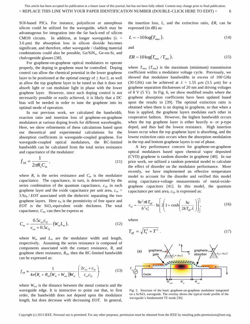
basic graphene-on-graphene optical modulator design is
shown in Fig. 5 [36]. This device structure consists of a
waveguide (which is generally silicon, but could also be made
out of numerous other materials depending upon the
application), a dielectric spacer layer above the waveguide, a
first layer of graphene, a second dielectric layer and then a
second layer of graphene. The lower dielectric layer should be
as thin as possible to ensure optimal absorption in the
graphene, while the thickness of the insulator separating the
two graphene layers can be optimized, depending upon the
requirements of the application. Such dielectric layers could
consist of SiO2, high- dielectrics such as HfO2, or other
materials such as hexagonal boron nitride (BN) [37]. Ohmic
contacts to the two graphene layers are made to the side of the
waveguide at sufficient distances to avoid excessive optical
losses by absorption in the metal contacts. A standard silicon-
on-insulator (SOI) substrate can be used to fabricate the
waveguide layer for use in a spectral range from = 1.1 μm to
mid-infrared with wavelength up to = 3.6 μm. However, due
to the fact that no electrical contact is made to the waveguide
material, much greater flexibility in the choice of the
waveguide and cladding materials exists compared to standard
Fig. 4. Graphene integrated in three types of silicon waveguides: 110-nm
and 220-nm-thick strip waveguides and horizontal slot waveguide. The
contour plot of horizontal electrical field shows the fundamental TE modes
of the waveguides. Graphene absorption coefficients up to 0.2 dB/m can
be obtained with the slot waveguide.
Copyright (c) 2013 IEEE. Personal use is permitted. For any other purposes, permission must be obtained from the IEEE by emailing [email protected].
This article has been accepted for publication in a future issue of this journal, but has not been fully edited. Content may change prior to final publication.
> REPLACE THIS LINE WITH YOUR PAPER IDENTIFICATION NUMBER (DOUBLE-CLICK HERE TO EDIT) <
6
SOI-based PICs. For instance, polysilicon or amorphous
silicon could be utilized for the waveguide, which may be
advantageous for integration into the far back-end of silicon
CMOS circuits. In addition, at longer waveguides ( >
3.6 μm) the absorption loss in silicon dioxide becomes
significant, and therefore, other waveguide / cladding material
combinations could also be possible, Ge/SiNx, Ge-on-Si, and
chalcogenide glasses [38].
For graphene-on-graphene optical modulators to operate
properly, the doping in graphene must be controlled. Doping
control can allow the chemical potential in the lower graphene
layer to be positioned at the optimal energy of + ħ / 2, as well
as allow the top graphene layer to be tuned so that it does not
absorb light or can modulate light in phase with the lower
graphene layer. However, since such doping control is not
necessarily possible or easily achieved, it is likely that a DC
bias will be needed in order to tune the graphene into its
optimal mode of operation.
In our previous work, we calculated the bandwidth,
exaction ratio and insertion loss of graphene-on-graphene
modulators at various doping levels for different wavelengths.
Here, we show refinements of these calculations based upon
our theoretical and experimental calculations for the
absorption coefficients in waveguide-coupled graphene. For
waveguide-coupled optical modulators, the RC-limited
bandwidth can be calculated from the total series resistance
and capacitance of the modulator:
ms
BCR
f2
13 , (11)
where Rs is the series resistance and Cm is the modulator
capacitance. The capacitance, in turn, is determined by the
series combination of the quantum capacitance, cQ, in each
graphene layer and the oxide capacitance per unit area, cox =
3.90 / EOT associated with the dielectric separating the two
graphene layers. Here 0 is the permittivity of free space and
EOT is the SiO2-equivalent oxide thickness. The total
capacitance, Cm, can then be express as
mm
Qox
Qox
m LWcc
ccC
5.0
5.0, (12)
where Wm and Lm are the modulator width and length,
respectively. Assuming the series resistance is composed of
components associated with the contact resistance, Rc and
graphene sheet resistance, Rsh, then the RC-limited bandwidth
can be expressed as:
Qox
Qox
mextmshc
Bcc
cc
WWWRRf
2
4
13
, (13)
where Wext is the distance between the metal contacts and the
waveguide edge. It is instructive to point out that, to first
order, the bandwidth does not depend upon the modulator
length, but does decrease with decreasing EOT. In general,
the insertion loss, L, and the extinction ratio, ER, can be
expressed (in dB) as:
maxlog10 TL , (14)
and
minmax /log10 TTER , (15)
where Tmax (Tmin) is the maximum (minimum) transmission
coefficient within a modulator voltage cycle. Previously, we
showed that modulator bandwidths in excess of 100 GHz
(30 GHz) can be achieved at = 1.55 m (3.5 m) for a
graphene separation thicknesses of 20 nm and driving voltages
of 8 V (5 V). In Fig. 6, we show modified results where the
graphene absorption coefficients have been updated based
upon the results in [39]. The optimal extinction ratio is
obtained when there is no doping in graphene, so that when a
bias is applied, the graphene layers modulate each other in
cooperative fashion. However, the highest bandwidth occurs
when the top graphene layer is either heavily n- or p-type
doped, and thus had the lowest resistance. High insertion
losses occur when the top graphene layer is absorbing, and the
lowest extinction ratio occurs when the absorption modulation
in the top and bottom graphene layers is out of phase.
A key performance concern for graphene-on-graphene
optical modulators based upon chemical vapor deposited
(CVD) graphene is random disorder in graphene [40]. In our
prior work, we utilized a random potential model to calculate
the effect of disorder on the modulator performance. More
recently, we have implemented an effective temperature
model to account for the disorder and verified this model
using capacitance-voltage measurements of metal-oxide-
graphene capacitors [41]. In this model, the quantum
capacitance per unit area, cQ, is expressed as:
,2
cosh12ln8
22
2
effF
eff
QkT
hc
vh
kTec (16)
where
22
0 TTTeff . (17)
Fig. 5. Structure of the basic graphene-on-graphene modulator integrated on a Si/SiO2 waveguide. The overlay shows the typical mode profile of the
waveguide’s fundamental TE mode [36].
Copyright (c) 2013 IEEE. Personal use is permitted. For any other purposes, permission must be obtained from the IEEE by emailing [email protected].
This article has been accepted for publication in a future issue of this journal, but has not been fully edited. Content may change prior to final publication.
> REPLACE THIS LINE WITH YOUR PAPER IDENTIFICATION NUMBER (DOUBLE-CLICK HERE TO EDIT) <
7
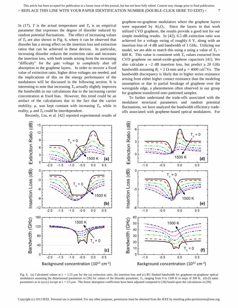
In (17), T is the actual temperature and T0 is an empirical
parameter that expresses the degree of disorder induced by
random potential fluctuations. The effect of increasing values
of T0 are also shown in Fig. 6, where it can be observed that
disorder has a strong effect on the insertion loss and extinction
ratios that can be achieved in these devices. In particular,
increasing disorder reduces the extinction ratio and increases
the insertion loss, with both trends arising from the increasing
“difficulty” for the gate voltage to completely shut off
absorption in the graphene layers. In order to recover a fixed
value of extinction ratio, higher drive voltages are needed, and
the implications of this on the energy performance of the
modulators will be discussed in the following section. It is
interesting to note that increasing T0 actually slightly improves
the bandwidth in our calculations due to the increasing carrier
concentration at fixed bias. However, this trend could be an
artifact of the calculations due to the fact that the carrier
mobility, , was kept constant with increasing T0, while in
reality, and T0 could be interdependent.
Recently, Liu, et al. [42] reported experimental results of
graphene-on-graphene modulators where the graphene layers
were separated by Al2O3. Since the layers in that work
utilized CVD graphene, the results provide a good test for our
simple modeling results. In [42], 6.5 dB extinction ratio was
achieved for a voltage swing of roughly 6 V, along with an
insertion loss of -4 dB and bandwidth of 1 GHz. Utilizing our
model, we are able to match this using a using a value of T0 ~
600 K. This value is consistent with T0 values extracted from
CVD graphene on metal-oxide-graphene capacitors [41]. We
also calculate a 2 dB insertion loss, but predict a 20 GHz
bandwidth assuming Rc = 2 -mm and = 4000 cm2/Vs. The
bandwidth discrepancy is likely due to higher series resistance
arising from either higher contact resistance than the modeling
assumption or due to partial breakage of graphene over the
waveguide edge, a phenomenon often observed in our group
for graphene transferred onto patterned samples.
To further understand the trade-offs associated with the
modulator structural parameters and random potential
fluctuations, we have analyzed the bandwidth efficiency trade-
offs associated with graphene-based optical modulators. For
Fig. 6. (a) Calculated values at = 1.55 m for the (a) extinction ratio, (b) insertion loss and (c) RC-limited bandwidth for graphene-on-graphene optical
modulators assuming the dimensional parameters in [36] for values of the disorder parameter, T0, ranging from 0 to 1500 K in steps of 300 K. (d)-(f) same
parameters as in (a)-(c) except at = 3.5 m. The linear absorption coefficients have been adjusted compared to [36] based upon the calculations in [39].
Copyright (c) 2013 IEEE. Personal use is permitted. For any other purposes, permission must be obtained from the IEEE by emailing [email protected].
This article has been accepted for publication in a future issue of this journal, but has not been fully edited. Content may change prior to final publication.
> REPLACE THIS LINE WITH YOUR PAPER IDENTIFICATION NUMBER (DOUBLE-CLICK HERE TO EDIT) <
8
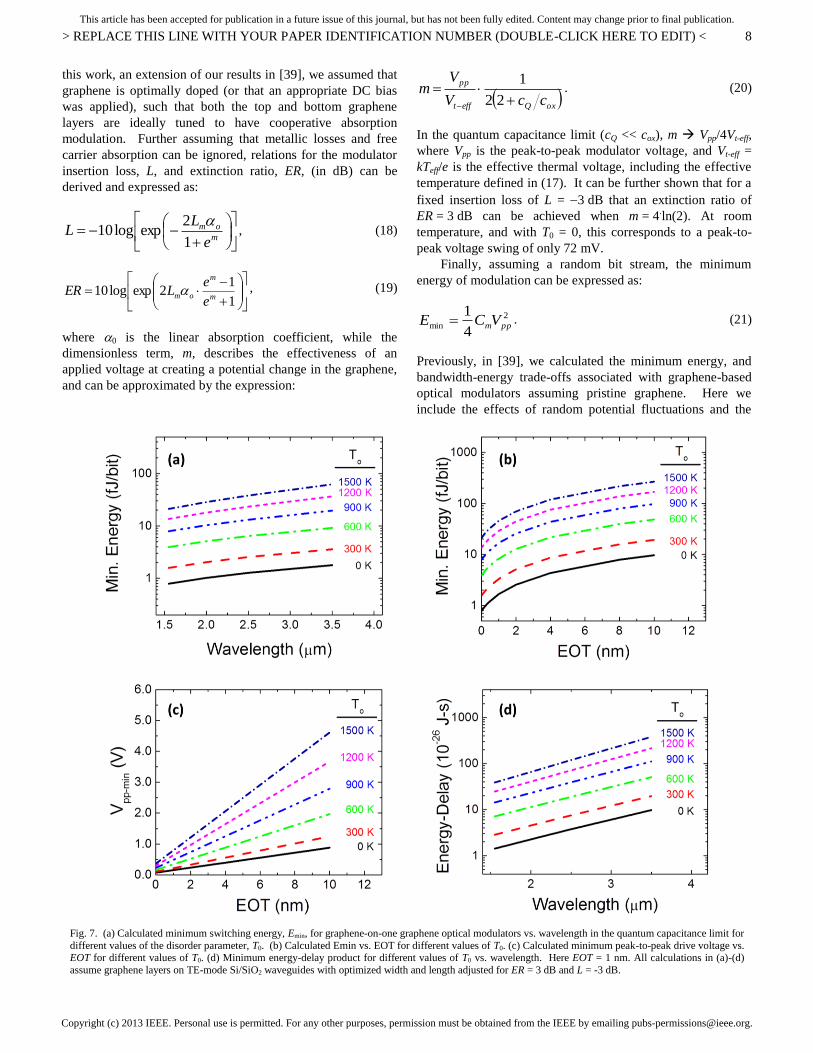
this work, an extension of our results in [39], we assumed that
graphene is optimally doped (or that an appropriate DC bias
was applied), such that both the top and bottom graphene
layers are ideally tuned to have cooperative absorption
modulation. Further assuming that metallic losses and free
carrier absorption can be ignored, relations for the modulator
insertion loss, L, and extinction ratio, ER, (in dB) can be
derived and expressed as:
m
om
e
LL
1
2explog10
, (18)
1
12explog10
m
m
ome
eLER , (19)
where 0 is the linear absorption coefficient, while the
dimensionless term, m, describes the effectiveness of an
applied voltage at creating a potential change in the graphene,
and can be approximated by the expression:
oxQefft
pp
ccV
Vm
22
1. (20)
In the quantum capacitance limit (cQ << cox), m Vpp/4Vt-eff,
where Vpp is the peak-to-peak modulator voltage, and Vt-eff =
kTeff/e is the effective thermal voltage, including the effective
temperature defined in (17). It can be further shown that for a
fixed insertion loss of L = 3 dB that an extinction ratio of
ER = 3 dB can be achieved when m = 4.ln(2). At room
temperature, and with T0 = 0, this corresponds to a peak-to-
peak voltage swing of only 72 mV.
Finally, assuming a random bit stream, the minimum
energy of modulation can be expressed as:
2
min4
1ppmVCE . (21)
Previously, in [39], we calculated the minimum energy, and
bandwidth-energy trade-offs associated with graphene-based
optical modulators assuming pristine graphene. Here we
include the effects of random potential fluctuations and the
Fig. 7. (a) Calculated minimum switching energy, Emin, for graphene-on-one graphene optical modulators vs. wavelength in the quantum capacitance limit for
different values of the disorder parameter, T0. (b) Calculated Emin vs. EOT for different values of T0. (c) Calculated minimum peak-to-peak drive voltage vs. EOT for different values of T0. (d) Minimum energy-delay product for different values of T0 vs. wavelength. Here EOT = 1 nm. All calculations in (a)-(d)
assume graphene layers on TE-mode Si/SiO2 waveguides with optimized width and length adjusted for ER = 3 dB and L = -3 dB.
Copyright (c) 2013 IEEE. Personal use is permitted. For any other purposes, permission must be obtained from the IEEE by emailing [email protected].
This article has been accepted for publication in a future issue of this journal, but has not been fully edited. Content may change prior to final publication.
> REPLACE THIS LINE WITH YOUR PAPER IDENTIFICATION NUMBER (DOUBLE-CLICK HERE TO EDIT) <
9
results are summarized in Fig. 7. In all plots shown in Fig. 7,
the insertion loss and extinction ratio are fixed at L = 3 dB
and ER = 3 dB, respectively.
In Fig. 7(a), the minimum switching energy in the quantum
capacitance limit (EOT 0) is plotted vs. wavelength for
increasing disorder, represented by increasing T0. The
minimum energy at = 1.55 m is less than 1 fJ/bit, which is
largely due to the extremely-small voltage needed for
modulation. The increasing energy at longer wavelengths is a
result of the wider waveguides needed at longer wavelengths
as well as the reduced linear absorption coefficient.
Increasing the disorder is shown increase the energy
consumption required to provide fixed performance, with
Emin ~ 4 fJ/bit for T0 = 600 K, but still less than 10 fJ/bit for
T0 = 900 K. Of course, having EOT 0 is impractical and
some thickness of dielectric is needed for practical devices.
Due to the fact that it is the Fermi-level movement within
graphene that leads to optical modulation, any voltage drop in
the region between the layers is “wasted.” Therefore, the
switching energy increases with increasing EOT as shown in
Fig. 7(b). Nevertheless, for realistic values of EOT = 2 nm and
T0 = 600 K, values of Emin ~ 10 fJ/bit remain achievable. Fig.
7(c) shows the associated voltages need to achieve L = 3 dB
and ER = 3 dB, respectively, and the plot indicates that
increasing disorder and EOT increase the modulation voltages
required. Finally, even though reducing the value of EOT
improves the energy efficiency of the modulator, because of
the fact that the resistance does not scale as the capacitance is
increased, the bandwidth is reduced with lower EOT. This
results in a fundamental bandwidth-efficiency trade-off, and
values of the energy-delay product calculated for different
values of T0 and at different wavelengths are shown in
Fig. 7(d). For these calculations, EOT was fixed at 1 nm. A
key potential advantage of graphene-based optical modulators
is their low voltage of operation compared to other types of
modulators, such as many Si and Si/Ge based devices.
Therefore, minimization of the random potential fluctuations,
and thus T0, will be critical in the future to realize the full
benefits of graphene-based optical modulators.
C. Photodetectors and other devices
The strong and broadband inter-band absorption and high
room-temperature carrier mobility in graphene suggest it can
be utilized for broadband, ultrafast photodetection. It has been
predicted that the operational wavelength range of graphene
photodetectors should range from 300 nm to 6 m or longer.
In the near-IR, graphene detectors have demonstrated
bandwidths as high as 40 GHz in a normal-incidence
configuration. The intrinsic bandwidth of graphene
photodetectors is predicted to be up to 500 GHz [18].
However, normal-incidence graphene photodetectors suffer
from very low responsivity of only 1.5 mA/W when unbiased
and ~ 6 mA/W when a bias voltage is applied [19]. To
improve the responsivity, optical cavities [43] and quantum
dots [44] have been integrated with graphene, but these
approaches sacrifice the detector’s bandwidth or speed. Dark
current is a significant concern for graphene photodetectors.
Due to the gapless nature of graphene, operating a
photodetector with an applied bias voltage results in a large
dark current and is thus undesirable for realistic applications.
Therefore, practical graphene photodetectors must operate at
zero bias. This requirement means that a built-in field needs
to be created between the contacts, so that the photogenerated
carriers can be swept to the electrodes before recombining,
and can be accomplished by using electrodes of different work
functions [19]. Furthermore, the graphene chemical potential
needs to be “tuned” to be near the Dirac energy, to ensure
maximum field penetration into the graphene [19]. In addition
to photovoltaic generation of carriers, photo-thermoelectric
and hot carrier effects also play important roles in graphene
photodetectors and can augment the detection responsivity if
the doping level in the graphene and the contact regions can be
optimally controlled [45,46].
Use of a waveguide integrated photodetector is promising
to augment the responsivity without the compromises of other
approaches. As discussed earlier, the reduced optical field
overlap with graphene can be compensated by a very long
interaction length. An integrated structure similar to that used
in the optical modulator demonstrated by Liu et. al. [17] can
be used. The optical loss due to metal contacts, however,
needs to be minimized.
The Dirac spectrum of electron-hole systems in graphene
also leads to very interesting new surface modes of
electromagnetic waves propagating in graphene that are highly
sensitive to the relative contributions of inter- and intra- band
transitions to the total complex conductivity. The intra-band
contribution of the dynamic conductivity in Equation (1) is
similar to the Drude conductivity of other 2D electron systems
including metal surfaces and 2D electron gases in
semiconductor quantum wells [47]. In these electron systems,
it is well-known that only TM modes (surface plasmons) are
supported and propagate. This can be determined from the
boundary conditions when the imaginary part of conductivity
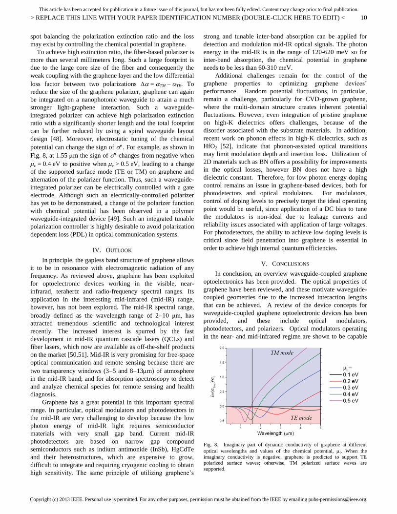
is positive (intra > 0) [29,30]. In graphene, however, the
inter-band transitions contribute to the dynamic conductivity
with a negative value of imaginary conductivity, as shown in
Fig. 2. When ħ / 2 > |c| inter-band contributions dominate
so the total imaginary conductivity is negative ( < 0) as
shown in Fig. 8. It is predicted that, in this regime, only TE
surface modes can exist while the TM mode is no longer
supported and thus will have a high loss [30]. Bao et al.
utilized such an effect to implement a fiber integrated
graphene polarizer [20]. The device includes monolayer and
few-layer graphene transferred on an optical fiber with an
exposed core. Because CVD-grown graphene with high p-type
doping is used, the condition < 0 is satisfied over a wide
spectral window. Therefore, only the TE modes (guided and
leaky modes) can couple and be weakly guided at the fiber
graphene interface while the TM modes will suffer a high loss.
This difference in propagation loss between two types of
modes leads to polarizing of the input light. An extinction
ratio of 27 dB at telecommunication band is reported although
the 5 dB insertion loss due to graphene is relative high. Such a
loss is inevitable because of inter-band absorption but a sweet
Copyright (c) 2013 IEEE. Personal use is permitted. For any other purposes, permission must be obtained from the IEEE by emailing [email protected].
This article has been accepted for publication in a future issue of this journal, but has not been fully edited. Content may change prior to final publication.
> REPLACE THIS LINE WITH YOUR PAPER IDENTIFICATION NUMBER (DOUBLE-CLICK HERE TO EDIT) <
10
spot balancing the polarization extinction ratio and the loss
may exist by controlling the chemical potential in graphene.
To achieve high extinction ratio, the fiber-based polarizer is
more than several millimeters long. Such a large footprint is
due to the large core size of the fiber and consequently the
weak coupling with the graphene layer and the low differential
loss factor between two polarizations = TM – TE. To
reduce the size of the graphene polarizer, graphene can again
be integrated on a nanophotonic waveguide to attain a much
stronger light-graphene interaction. Such a waveguide-
integrated polarizer can achieve high polarization extinction
ratio with a significantly shorter length and the total footprint
can be further reduced by using a spiral waveguide layout
design [48]. Moreover, electrostatic tuning of the chemical
potential can change the sign of . For example, as shown in
Fig. 8, at 1.55 m the sign of changes from negative when
c = 0.4 eV to positive whenc > 0.5 eV, leading to a change
of the supported surface mode (TE or TM) on graphene and
alternation of the polarizer function. Thus, such a waveguide-
integrated polarizer can be electrically controlled with a gate
electrode. Although such an electrically-controlled polarizer
has yet to be demonstrated, a change of the polarizer function
with chemical potential has been observed in a polymer
waveguide-integrated device [49]. Such an integrated tunable
polarization controller is highly desirable to avoid polarization
dependent loss (PDL) in optical communication systems.
IV. OUTLOOK
In principle, the gapless band structure of graphene allows
it to be in resonance with electromagnetic radiation of any
frequency. As reviewed above, graphene has been exploited
for optoelectronic devices working in the visible, near-
infrarad, terahertz and radio-frequency spectral ranges. Its
application in the interesting mid-infrared (mid-IR) range,
however, has not been explored. The mid-IR spectral range,
broadly defined as the wavelength range of 210 μm, has
attracted tremendous scientific and technological interest
recently. The increased interest is spurred by the fast
development in mid-IR quantum cascade lasers (QCLs) and
fiber lasers, which now are available as off-the-shelf products
on the market [50,51]. Mid-IR is very promising for free-space
optical communication and remote sensing because there are
two transparency windows (35 and 813m) of atmosphere
in the mid-IR band; and for absorption spectroscopy to detect
and analyze chemical species for remote sensing and health
diagnosis.
Graphene has a great potential in this important spectral
range. In particular, optical modulators and photodetectors in
the mid-IR are very challenging to develop because the low
photon energy of mid-IR light requires semiconductor
materials with very small gap band. Current mid-IR
photodetectors are based on narrow gap compound
semiconductors such as indium antimonide (InSb), HgCdTe
and their heterostructures, which are expensive to grow,
difficult to integrate and requiring cryogenic cooling to obtain
high sensitivity. The same principle of utilizing graphene’s
strong and tunable inter-band absorption can be applied for
detection and modulation mid-IR optical signals. The photon
energy in the mid-IR is in the range of 120-620 meV so for
inter-band absorption, the chemical potential in graphene
needs to be less than 60-310 meV.
Additional challenges remain for the control of the
graphene properties to optimizing graphene devices’
performance. Random potential fluctuations, in particular,
remain a challenge, particularly for CVD-grown graphene,
where the multi-domain structure creates inherent potential
fluctuations. However, even integration of pristine graphene
on high-K dielectrics offers challenges, because of the
disorder associated with the substrate materials. In addition,
recent work on phonon effects in high-K dielectrics, such as
HfO2 [52], indicate that phonon-assisted optical transitions
may limit modulation depth and insertion loss. Utilization of
2D materials such as BN offers a possibility for improvements
in the optical losses, however BN does not have a high
dielectric constant. Therefore, for low photon energy doping
control remains an issue in graphene-based devices, both for
photodetectors and optical modulators. For modulators,
control of doping levels to precisely target the ideal operating
point would be useful, since application of a DC bias to tune
the modulators is non-ideal due to leakage currents and
reliability issues associated with application of large voltages.
For photodetectors, the ability to achieve low doping levels is
critical since field penetration into graphene is essential in
order to achieve high internal quantum efficiencies.
V. CONCLUSIONS
In conclusion, an overview waveguide-coupled graphene
optoelectronics has been provided. The optical properties of
graphene have been reviewed, and these motivate waveguide-
coupled geometries due to the increased interaction lengths
that can be achieved. A review of the device concepts for
waveguide-coupled graphene optoelectronic devices has been
provided, and these include optical modulators,
photodetectors, and polarizers. Optical modulators operating
in the near- and mid-infrared regime are shown to be capable
Fig. 8. Imaginary part of dynamic conductivity of graphene at different
optical wavelengths and values of the chemical potential, c. When the
imaginary conductivity is negative, graphene is predicted to support TE polarized surface waves; otherwise, TM polarized surface waves are
supported.
Copyright (c) 2013 IEEE. Personal use is permitted. For any other purposes, permission must be obtained from the IEEE by emailing [email protected].
This article has been accepted for publication in a future issue of this journal, but has not been fully edited. Content may change prior to final publication.
> REPLACE THIS LINE WITH YOUR PAPER IDENTIFICATION NUMBER (DOUBLE-CLICK HERE TO EDIT) <
11
of bandwidths above 100 GHz and 30 GHz, respectively.
Doping control is shown to be important to maximize the
extinction ratio and minimize insertion loss. Graphene optical
modulators are shown to be capable of energy consumption of
less than 1 fJ/bit in the ideal quantum capacitance limit using
pristine graphene. However, random potential fluctuations
and practical device geometries could increase this value by
roughly a factor of 10. Motivation for waveguide coupling in
other graphene-based devices is also provided and these
devices include photodetectors and optical polarizers.
Graphene devices have tremendous potential as a platform for
broadband photonic integrated circuits and if continued
improvement in the material quality and integration processes
for graphene-on-waveguide structures can be made, then the
outlook is good that such potential can be realized.
REFERENCES
[1] Y.-M. Lin, H.-Y. Chiu, K. A. Jenkins, D. B. Farmer, P. Avouris, and A.
Valdes-Garcia, “Dual-gate graphene FETs with fT of 50 GHz,” IEEE
Elect. Dev. Lett., vol. 31, pp. 68-70, Jan 2010. [2] H. Wang, D. Nezich, J. Kong, and T. Palacios, “Graphene frequency
multipliers,” IEEE Elect. Dev. Lett., vol. 30, pp. 547-549, May 2009.
[3] B. Sensale-Rodriguez, Y. Rusen, K. M. M., F. Tian, T. Kristof, H. W. Sik, J. Debdeep, L. Lei, and X. H. Grace, “Broadband graphene terahertz
modulators enabled by intraband transitions,” Nature Commun., vol. 3,
780, 2012. [4] Q. Zhang, Y. Lu, H. G. Xing, S. J. Koester, and S. O. Koswatta,
“Scalability of atomic-thin-body (ATB) transistors based on graphene
nanoribbons,” IEEE Elect. Dev. Lett., vol. 31, pp. 531-533, Jun 2010. [5] S. J. Koester, “High quality factor graphene varactors for wireless
sensing applications,” Appl. Phys. Lett., vol. 99, 163105, 2011.
[6] K. I. Bolotin, K. J. Sikes, Z. Jiang, M. Klima, G. Fudenberg, J. Hone, P. Kim, and H. L. Stormer, “Ultrahigh electron mobility in suspended
graphene,” Solid State Commun., vol. 146, pp. 351-355, 2008.
[7] A. A. Balandin, S. Ghosh, W. Z. Bao, I. Calizo, D. Teweldebrhan, F. Miao, and C. N. Lau, “Superior thermal conductivity of single-layer
graphene,” Nano Lett., vol. 8, pp. 902-907, 2008.
[8] C. Lee, X. D. Wei, J. W. Kysar, and J. Hone, “Measurement of the elastic properties and intrinsic strength of monolayer graphene,”
Science, vol. 321, pp. 385-388, 2008.
[9] K. S. Novoselov, A. K. Geim, S. V. Morozov, D. Jiang, M. I. Katsnelson, I. V. Grigorieva, S. V. Dubonos, and A. A. Firsov, “Two-
dimensional gas of massless Dirac fermions in graphene,” Nature, vol.
438, pp. 197-200, 2005. [10] R. R. Nair, P. Blake, and A. N. Grigorenko, “Fine structure constant
defines visual transparency of graphene,” Science, vol. 320, pp. 5881,
2008. [11] F. Wang, Z. Yuanbo, T. Chuanshan, G. Caglar, Z. Alex, C. Michael, and
S. Y. Ron, “Gate-variable optical transitions in graphene,” Science, vol.
320, pp. 206-209, 2008. [12] Q. Bao, H. Zhang, Y. Wang, Z. Ni, Y. Yan, Z. X. Shen, K. P. Loh, and
D. Y. Tang, “Atomic-layer graphene as a saturable absorber for ultrafast
pulsed lasers,” Adv. Func. Materials, vol. 19, pp. 3077-3083, 2009. [13] V. Ryzhii, M. Ryzhii, V. Mitin, and T. Otsuji, “Terahertz and infrared
photodetection using p-i-n multiple-graphene-layer structures,” J. Appl. Phys., vol. 107, 054512, 2010.
[14] X. Li, W. Cai, J. An, S. Kim, J. Nah, D. Yang, R. Piner, A.
Velamakanni, I. Jung, E. Tutuc, S. K. Banerjee, L. Colombo, and R. S. Ruoff, “Large-area synthesis of high-quality and uniform graphene films
on copper foils,” Science, vol. 324, pp. 1312-1314, 2009.
[15] F. Wang, Y. Zhang, C. Tian, C. Girit, A. Zettl, M. Crommie, and Y. R. Shen, “Gate-variable optical transitions in graphene,” Science, vol. 320,
pp. 206-209, 2008.
[16] Z. Q. Li, E. A. Henriksen, Z. Jiang, Z. Hao, M. C. Martin, P. Kim, H. L. Stormer, and D. N. Basov, “Dirac charge dynamics in graphene by
infrared spectroscopy,” Nature Phys., vol. 4, pp. 532-535, 2008.
[17] M. Liu, X. Yin, E. Ulin-Avila, B. Geng, T. Zentgraf, L. Ju, F. Wang, and X. Zhang, “A graphene-based broadband optical modulator,” Nature,
vol. 474, pp. 64-67, 2011.
[18] F. Xia, T. Mueller, Y. M. Lin, A. Valdes-Garcia, and P. Avouris,
“Ultrafast graphene photodetector,” Nature Nanotech., vol. 4, pp. 839-43, 2009.
[19] T. Mueller, F. Xia, and P. Avouris, “Graphene photodetectors for high-
speed optical communications,” Nature Photon., vol. 4, pp. 297-301, 2010.
[20] Q. L. Bao, H. Zhang, B. Wang, Z. H. Ni, C. H. Y. X. Lim, Y. Wang, D.
Y. Tang, and K. P. Loh, “Broadband graphene polarizer,” Nature Photon., vol. 5, pp. 411-415, 2011.
[21] Z. Sun, T. Hasan, F. Torrisi, D. Popa, G. Privitera, F. Wang, F.
Bonaccorso, D. M. Basko, and A. C. Ferrari, “Graphene mode-locked ultrafast laser,” ACS Nano, vol. 4, pp. 803-810, 2010.
[22] T. Ando, Y. Zheng, and H. Suzuura, “Dynamical conductivity and zero-
mode anomaly in honeycomb lattices,” J. Phys. Soc. Japan, vol. 71, pp. 1318-1324, 2002.
[23] M. Lipson, “Silicon photonics: the optical spice rack,” Electron. Lett.,
vol. 45, pp. 575-577, 2009. [24] D. Liang and J. E. Bowers, “Recent progress in lasers on silicon,”
Nature Photon., vol. 4, pp. 511-517, 2010.
[25] J. Michel, J. F. Liu, and L. C. Kimerling, “High-performance Ge-on-Si photodetectors,” Nature Photon., vol. 4, pp. 527-534, 2010.
[26] Q. Bao and K. P. Loh, “Graphene photonics, plasmonics, and broadband
optoelectronic devices,” ACS Nano, vol. 6, pp. 3677-3694, 2012.
[27] A. Vakil and N. Engheta, “Transformation optics using graphene,”
Science, vol. 332, pp. 1291-1294, 2011.
[28] V. Gusynin, S. Sharapov, and J. Carbotte, “Sum rules for the optical and Hall conductivity in graphene,” Phys. Rev. B, vol. 75, 165407, 2007.
[29] G. W. Hanson, “Dyadic Green’s functions and guided surface waves for a surface conductivity model of graphene,” J. Appl. Phys., vol. 103,
064302, 2008.
[30] S. Mikhailov and K. Ziegler, “New electromagnetic mode in graphene,” Phys. Rev. Lett., vol. 99, 016803, 2007.
[31] A. Kuzmenko, E. van Heumen, F. Carbone, and D. van der Marel,
“Universal optical conductance of graphite,” Phys. Rev. Lett., vol. 100, 117401, 2008.
[32] R. R. Nair, P. Blake, A. N. Grigorenko, K. S. Novoselov, T. J. Booth, T.
Stauber, N. M. Peres, and A. K. Geim, “Fine structure constant defines visual transparency of graphene,” Science, vol. 320, p. 1308, 2008.
[33] H. Li, Y. Anugrah, S. J. Koester, and M. Li, “Optical absorption in
graphene integrated on silicon waveguides,” Appl. Phys. Lett., vol. 101, 111110, 2012.
[34] R. A. Soref and B. R. Bennett, “Electrooptical effects in silicon,” IEEE
J. Quant. Electron., vol. 23, pp. 123-129, Jan 1987.
[35] Q. F. Xu, B. Schmidt, S. Pradhan, and M. Lipson, “Micrometre-scale
silicon electro-optic modulator,” Nature, vol. 435, pp. 325-327, 2005.
[36] S. J. Koester and M. Li, “High-speed waveguide-coupled graphene-on-graphene optical modulators,” Appl. Phys. Lett., vol. 100, 171107, 2012.
[37] Z. Liu, L. Song, S. Z. Zhao, J. Q. Huang, L. L. Ma, J. N. Zhang, J. Lou,
and P. M. Ajayan, “Direct growth of graphene/hexagonal boron nitride stacked layers,” Nano Lett., vol. 11, pp. 2032-2037, 2011.
[38] R. Soref, “Mid-infrared photonics in silicon and germanium,” Nature
Photon., vol. 4, pp. 495-497, 2010. [39] S. J. Koester, H. Li, and M. Li, “Switching energy limits of waveguide-
coupled graphene-on-graphene optical modulators,” Optics Express, vol.
20, pp. 20330-20341, 2012. [40] Y. B. Zhang, V. W. Brar, C. Girit, A. Zettl, and M. F. Crommie, “Origin
of spatial charge inhomogeneity in graphene,” Nature Phys., vol. 5, pp.
722-726, 2009. [41] M. A. Ebrish, D. A. Deen, and S. J. Koester, “Border trap
characterization in metal-oxide-graphene capacitors with HfO2
dielectrics,” 71st Device Research Conference, Jun. 24-26 2013. [42] M. Liu, X. B. Yin, and X. Zhang, “Double-layer graphene optical
modulator,” Nano Lett., vol. 12, pp. 1482-1485, Mar 2012.
[43] M. Furchi, A. Urich, A. Pospischil, G. Lilley, K. Unterrainer, H. Detz, P. Klang, A. M. Andrews, W. Schrenk, G. Strasser, and T. Mueller,
“Microcavity-integrated graphene photodetector,” Nano Lett., vol. 12,
pp. 2773-2777, 2012. [44] G. Konstantatos, M. Badioli, L. Gaudreau, J. Osmond, M. Bernechea, F.
P. G. de Arquer, F. Gatti, and F. H. L. Koppens, “Hybrid graphene-
quantum dot phototransistors with ultrahigh gain,” Nature Nanotech., vol. 7, pp. 363-368, 2012.
[45] X. Xu, N. M. Gabor, J. S. Alden, A. M. van der Zande, and P. L.
McEuen, “Photo-thermoelectric effect at a graphene interface junction,” Nano Lett., vol. 10, pp. 562-566, 2009.
Copyright (c) 2013 IEEE. Personal use is permitted. For any other purposes, permission must be obtained from the IEEE by emailing [email protected].
This article has been accepted for publication in a future issue of this journal, but has not been fully edited. Content may change prior to final publication.
> REPLACE THIS LINE WITH YOUR PAPER IDENTIFICATION NUMBER (DOUBLE-CLICK HERE TO EDIT) <
12
[46] M. Freitag, T. Low, F. Xia, and P. Avouris, “Photoconductivity of
biased graphene,” Nature Photonics, vol. 7, pp. 53-59, 2012. [47] F. Stern, “Polarizability of a two-dimensional electron gas,” Phys. Rev.
Lett., vol. 18, pp. 546-548, 1967.
[48] J. F. Bauters, M. J. R. Heck, D. Dai, J. S. Barton, D. J. Blumenthal, and J. E. Bowers, “Ultralow-loss planar Si3N4 waveguide polarizers,” IEEE
Phot. Journ., vol. 5, 6600207, 2013.
[49] J. T. Kim and C.-G. Choi, “Graphene-based polymer waveguide polarizer,” Optics Express, vol. 20, pp. 3556-3556, 2012.
[50] Y. Yao, A. J. Hoffman, and C. F. Gmachl, “Mid-infrared quantum
cascade lasers,” Nature Photon., vol. 6, pp. 432-439, 2012. [51] S. D. Jackson, “Towards high-power mid-infrared emission from a fibre
laser,” Nature Phot., vol. 6, pp. 423-431, 2012.
[52] K. Zou, X. Hong, D. Keefer, and J. Zhu, “Deposition of high-quality HfO2 on graphene and the effect of remote oxide phonon scattering,”
Phys. Rev. Lett., vol. 105, 126601, 2010.
Steven J. Koester (M’96–SM’02)
received the B.S.E.E and M.S.E.E.
degrees from the University of Notre
Dame, Notre Dame, IN, in 1989 and
1991, respectively, and the Ph.D. degree,
in 1995, from the University of California,
Santa Barbara, where his research
involved the study of quantum transport in
InAs quasi-1-D structures.
He has been a Professor of Electrical and Computer
Engineering in the College of Science and Engineering at the
University of Minnesota, in Minneapolis, MN since 2010.
Prior to joining the University of Minnesota, he was a
Research Staff Member with the T. J. Watson Research
Center, IBM Research Division, Yorktown Heights, NY
where his work involved Si/SiGe devices and materials, high-
speed Ge photodetectors, and III-V MOSFETs. His most
recent position at IBM was Manager of Exploratory
Technology where his team investigated novel device and
integration solutions for post-22-nm node CMOS technology.
Dr. Koester’s current research involves investigations into
the device applications of graphene, including novel sensors,
spintronics, and optoelectronic devices. He has authored or
coauthored more than 160 technical publications and
conference presentations, and is the holder of 46 U.S. patents.
He was the general chair of the 2009 Device Research
Conference and is currently an associate editor of IEEE
Electron Device Letters.
Mo Li received the B.S. degree in Physics
from the University of Science and
Technology, China in 2001, the M.S.
degree in Physics from the University of
California, San Diego in 2003, and the
Ph.D. in Applied Physics, from the
California Institute of Technology in
2007.
He has been an Assistant Professor of
Electrical and Computer Engineering in the College of
Science and Engineering at the University of Minnesota, in
Minneapolis, MN since 2010. Prior to joining the University
of Minnesota he was a postdoctoral associate in the
Department of Electrical Engineering at Yale University from
2007 to 2010.
Dr. Li’s current research involves the development of nano-
opto-mechanical systems and waveguide-coupled graphene
optoelectronic devices. He received the McKnight Land-Grant
Professorship of the University of Minnesota in 2013 and the
AFOSR Young Investigator Award in 2012.
.

![Graphene Tribotronics for Electronic Skin and Touch …nesel.skku.edu/paper files/184.pdfGraphene has excellent electronic transport characteristics and is also transparent.[13,14]](https://static.fdocuments.in/doc/165x107/5eaf0a8957f05b3a867dc6ee/graphene-tribotronics-for-electronic-skin-and-touch-neselskkuedupaper-files184pdf.jpg)