Chapter 9 3D Fabrication Options for High-Performance...
21
Chapter 9 3D Fabrication Options for High-Performance CMOS Technology Anna W.Topol, Steven J. Koester, Douglas C. La Tulipe, and Albert M. Young 9.1 3-D Technology 9.1.1 Introduction The last several decades have seen an incredible increase in the functionality of computational systems. At its core, this capability has been driven by the scaling of semiconductor devices, from fractions of millimeters in the 1960s to tens of nanometers in today’s technologies. The scaling has enabled the number of transis- tors on a single chip to correspondingly grow at a geometric rate, roughly doubling every 18months; a trend is that now referred to as Moore’s law [1]. The impact of this trend cannot be underestimated and the resulting increase in computational capacity has had major impacts on almost every facet of society. For this reason, there is a tremendous push to continue along these same trends. However, several serious roadblocks exist. The first is the limits to lithographic scaling. The second is that power densities will not allow reliable systems to be fabricated even if lithographic scaling could continue. Therefore, it becomes a big challenge to increase system performance. Three dimensional (3D) integration technologies offer the promise of increasing system performance even in the absence of scaling. However, the main advantages of 3D integration can be summed up as follows: (1) 3D decreases the interconnect distance between regions of a chip, decreasing wiring parasitics and interconnect delay times, (2) 3D can dramatically increase the number of interconnects and there- fore increase the aggregate communication bandwidth between chips, and (3) 3D can allow dissimilar functions, technologies, and materials to be integrated. In the next part of this chapter we will talk about the 3D technology land- scape and focus on IBM’s wafer-level integration research and development (R&D) efforts. We will describe layer transfer processing and wafer-level thinning, discuss bonding and interconnection processes, and show successful implementation of the A.W. Topol IBM T. J. Watson Research Center, Yorktown Heights, NY, USA e-mail: [email protected] C.S. Tan et al. (eds.), Wafer-Level 3D ICs Process Technology, DOI: 10.1007/978-0-387-76534-1 9, C Springer Science+Business Media, LLC 2008 197
Transcript of Chapter 9 3D Fabrication Options for High-Performance...

Chapter 93D Fabrication Options for High-PerformanceCMOS Technology
Anna W. Topol, Steven J. Koester, Douglas C. La Tulipe,and Albert M. Young
9.1 3-D Technology
9.1.1 Introduction
The last several decades have seen an incredible increase in the functionality ofcomputational systems. At its core, this capability has been driven by the scalingof semiconductor devices, from fractions of millimeters in the 1960s to tens ofnanometers in today’s technologies. The scaling has enabled the number of transis-tors on a single chip to correspondingly grow at a geometric rate, roughly doublingevery 18 months; a trend is that now referred to as Moore’s law [1]. The impactof this trend cannot be underestimated and the resulting increase in computationalcapacity has had major impacts on almost every facet of society.
For this reason, there is a tremendous push to continue along these same trends.However, several serious roadblocks exist. The first is the limits to lithographicscaling. The second is that power densities will not allow reliable systems to befabricated even if lithographic scaling could continue. Therefore, it becomes a bigchallenge to increase system performance.
Three dimensional (3D) integration technologies offer the promise of increasingsystem performance even in the absence of scaling. However, the main advantagesof 3D integration can be summed up as follows: (1) 3D decreases the interconnectdistance between regions of a chip, decreasing wiring parasitics and interconnectdelay times, (2) 3D can dramatically increase the number of interconnects and there-fore increase the aggregate communication bandwidth between chips, and (3) 3Dcan allow dissimilar functions, technologies, and materials to be integrated.
In the next part of this chapter we will talk about the 3D technology land-scape and focus on IBM’s wafer-level integration research and development (R&D)efforts. We will describe layer transfer processing and wafer-level thinning, discussbonding and interconnection processes, and show successful implementation of the
A.W. TopolIBM T. J. Watson Research Center, Yorktown Heights, NY, USAe-mail: [email protected]
C.S. Tan et al. (eds.), Wafer-Level 3D ICs Process Technology,DOI: 10.1007/978-0-387-76534-1 9, C© Springer Science+Business Media, LLC 2008
197

198 A.W. Topol et al.
through-silicon via (TSV) process and Cu bonding for advanced microprocessorapplications.
The remainder of this chapter will describe our progress on one specific 3D inte-gration scheme based upon oxide fusion bonding. This technology is by no meansthe preferred-by-all 3D technology, but is perhaps ultimately the most capable tech-nology to achieve the highest density of 3D interconnects, and thus enables themost aggressive 3D architectures. The scheme could also be readily applicable tomultiple stack architectures, and it uses a conventional complementary metal-oxidesemiconductor (CMOS) processing approach. We describe the latest progress on thedevelopment of this technology, and also point out some of the remaining challengesneeded to bring it into manufacturing for mainstream CMOS applications.
9.1.2 Three-Dimensional Technology Landscape
At IBM, 3D integration is being pursued for various applications that have verydifferent technology requirements. As depicted in Fig. 9.1 these applications spanfrom 3D packaging to high-density 3D integrated circuit (IC) implementations.More specifically, for wireless communications, where TSVs are needed for makinglow-inductance contacts to the backside ground plane, a very low density of TSVsare required. More recently IBM has investigated 3D technology to integrate decou-pling capacitors with microprocessor to stabilize power delivery to the chips [2].In these applications, TSV densities on the order of the standard C4 (controlledcollapse chip connection flip-chip package) pitch are required. In the most extremecases, for highly integrated microprocessor configurations, a much higher densityof 3D vias are needed (105–106 pins cm–2 range) [3]. These requirements drive thehighest-density 3D processes that will be the main topic of the remainder of this
Via density(pins cm–2)
Wireless communication
Power grid stabilization
Microprocessor / memory stacks
Via size (μm)
102 103 104
200 50 10 1.0 0.20
3D Packaging High-density 3D
105 106
Fig. 9.1 Chart showing range of 3D technology applications being implemented at IBM
9 3D Fabrication Options 199
chapter. Data points in Fig. 9.1 are approximate but are representative of implemen-tations of 3D technologies that have been demonstrated by IBM or others, and hencethe via size and density values are not directly correlated.
9.1.3 Wafer-Level 3D Integration
Since many 3D integration research programs have been underway for years, sev-eral of the critical technology components have been demonstrated. As discussed inprevious chapters, these include low-cost fine via hole formation and highly reliablevia-filling technologies, bonding methodology, as well as layer transfer techniques.In addition, 3D-specific process equipment (such as bonding and alignment tools)and materials (such as good quality bonding mediums) are just now becoming avail-able. For some applications industry is beginning to move past the feasibility (R&D)phase into the commercialization phase. A TechSearch International report high-lights the major processes and materials used by various companies, and forecaststhe market for 3D integration [4]. Even though much work still remains to be accom-plished related to 3D design, in the areas of thermal and test issues for example,much progress has been made. In the end economic realities will determine if andin which markets the 3D technologies will be adopted.
Various 3D integration schemes have been developed using similar technologyelements. The main difference between these schemes relates to the choice of theso-called “face-to-back” or “face-to-face” options. The “face-to-back” method isbased on bonding the front side of the bottom wafer with the backside (usuallythinned) of the top wafer and correspondingly is often referred to as a “front side-to-backside” approach. The height of the structure and therefore the height of theinterconnecting via depends on the thickness of the thinned top wafer. Figure 9.2a–cillustrates various options for this technology based on bonding and via formationprocess assuming that silicon-on-insulator (SOI) wafers are used and hence all ofthe Si can be removed to provide for the shortest interwafer via connections.
Similarly the “face-to-face” approach focuses on joining the front sides of twowafers and hence is also referred to as “front side-to-front side” wafer-level transfer.Figure 9.2d–h depicts potential integration options assuming use of SOI wafers. Ifbulk wafers are used, the final structures would look similar except that they wouldcontain a thin layer of Si. As a consequence the minimum height of the intercon-necting via represented numerically on the right-hand side of all the structures inFig. 9.2 would have to be increased by at least a few microns (minimum reliableSi thinning process result). Due to processing limitations, as the height of the viaincreases the minimum width of the via has to increase as well to enable the subse-quent metallization process.
Assessment of various integration options is ongoing (e.g., Sematech in 2005initiated such an evaluation), as tool and process benchmarking develops and 3Dinfrastructure, materials, and unit processes mature [5]. Frequent technology ques-tions include: “Is there a one common approach to 3D integration and if not how todetermine which one should be used?” “What is driving the choice for particular 3D

200 A.W. Topol et al.
500nm145nm450nm
1095nm
Active Region Active Region
Si
BOXGate
Metal Line
Gate GateBottom wafer
Active Region Active RegionBOXGate
Metal Line
Gate Gate Via
Via
Top wafer
(a) Top wafer w/ bulk Si removed and inter-wafer viasfabricated before metal bonding
Si
Gate
Metal Line
Gate Gate
BOX
Metal Line
Gate Via
Via
-
500nm145nm450nm
1095nm
Active Region Active RegionBOXGate
Metal Line
Gate GateBottom wafer
Active Region Active RegionBOXGate
Metal Line
Gate Gate Via
Via
Top wafer
(b) Top wafer w/ bulk Si removed and inter-wafer viasfabricated after dielectric bonding
Si
BOXGate
Metal Line
Gate Gate
BOXGate
Metal Line
Gate Gateia
Si
145nm450nm
Active Region Active RegionBOXGate
Metal Line
Gate GateBottom wafer
Active Region Active RegionBOXGate
Metal Line
Gate GateVia
Via
Top wafer
595nm Metal Line
(c) Top wafer w/ bulk Si removed & interconnecting vias fabricated before or after metal bonding
Si
145nm
BOX
Metal Line
Metal Line
Via
Via
Metal Line
Si
Active Region Active RegionBOXGate
Metal Line
Gate Gate
450nm145nm BOX
Gate GateActive Region
Gate
595nm
Top wafer
Bottom wafer
Active RegionPlug
Plug
Metal Line
Metal Line
(d) Top wafer w/ bulk Si removed & interconnectingplugs fabricated after metal bonding
Si
Metal Line
BOXPlug
Plug
Metal Line
Metal Line
Si
Active Region Active RegionBOXGate
Metal Line
Gate Gate
450nm145nm BOX
Gate GateActive Region
Gate
895nm
Top wafer
Bottom wafer
Active RegionPlug
Plug
Metal Line
Via
Via
300nm
Metal Line
(e) Top wafer w/ bulk Si removed; plugs and inter-wafer vias fabricated after metal bonding
Si
Gate
Plug
Via
Si -
SiActive Region Active RegionBOX
Gate
Metal Line
Gate Gate
450nm145nm BOX
Gate GateActive Region
Gate
595nmTop
wafer
Bottom wafer
Active Region
Via
Plug
Via
Via
Via
Plug
Metal Line
~400nm
(f) Top wafer inter-wafer vias fabricated before metal bonding, then bulk Si is removed & metallized
Si
Active Region Active RegionBOXGate
Metal Line
Gate Gate
450nm145nm BOX
Gate GateGate
595nm
Active Region
Via
Plug
Via
Via
Via
Plug
Metal Line
~400nm
(f)Si
Si
Active Region Active RegionBOXGate
Metal Line
Gate Gate
450nm145nm BOX
Gate GateActive Region
Gate
300nmTop
wafer
Bottom wafer
Active RegionVia
Plug
Via
Plug
Metal Line
Via
300nm1195nm
(g) Top wafer w/ bulk Si removed & inter-wafer via fabricated before metal bonding
Si
Active Region Active RegionGate
Metal Line
Gate Gate
BOXGate
Active RegionGate
Via
Plug
Via
Plug
Metal Line
Via
-
Si
Active Region Active RegionBOXGate
Metal Line
Gate Gate
450nm145nm BOX
Gate GateActive Region
Gate
300nm
Top wafer
Bottom wafer
Active RegionVia
Plug
Via
Plug
Metal Line
Via
300nm1195nm
(h) Top wafer bulk Si removed and inter-wafer viasfabricated after dielectric bonding
Si
Active Region Active RegionGateGate Gate
Via
Plug
Via
Plug
-
Si
Fig. 9.2 Cross-sectional diagrams (a)–(c) show a final structure of potential “face-to-back” or“front side-to-backside” integration schemes; (d)–(h) depict “face-to-face” or “front side-to-frontside” 3D integration schemes. Numbers on the right side of the images highlight the minimumheight of interconnecting vias needed to provide electrical signal between the two wafers assuming90-nm SOI-based technology (buried oxide layer (BOX) of 1450 nm). Dashed lines in (b) and (h)indicate bonding interfaces
assembly technology?” “What materials and processes should be used?” “Shouldvias be formed during the wafer-stacking process or implemented later in the pro-cess? “What are the limiting factors to the adoption of various 3D technologies?”
As discussed in previous paragraphs, 3D integration process flow dependslargely on the application requirements. More specifically, based on the applica-tion specifications – which may include input/output (I/O) number and intercon-nect density, number of layers to be stacked, expected performance and bandwidthrequirements, cost, design limitations (including thermal and routing aspects), tech-nology choices (bulk vs. SOI etc.), or architectural level (device, macro, circuit,system, chip, package) – different 3D technology elements can be chosen. Specifi-cally the choice of bonding medium, use of carrier wafer, order of processing steps,incorporation of additional thermal cycles (such as curing, bond-strengthening, andoutgassing), choice of metallization techniques, implementation of seals, or any

9 3D Fabrication Options 201
other yield/reliability enhancers (such as via redundancy) are all dictated by appli-cation needs.
However, in general all 3D integration schemes which utilized the handle orcarrier wafer have six common technology elements. These are (1) a handle wafermethodology (e.g., a temporary bonding and release); (2) wafer thinning; (3) verticalinterconnects; (4) alignment; (5) bonding; and (6) final metallization and testing. Insections below we describe these elements, and give an update on the maturity oftheir implementation.
9.1.4 IBM 3D Integration Approaches
In the next two sections we will present two very specific applications of 3D tech-nology and discuss the rationale behind process options utilized to build these struc-tures. Both of these 3D constructions, namely system-level 3D implementations and3D circuits have been chosen as they represent two distinct cases of different 3Doptions for high-performance CMOS technology. The first application falls underthe microprocessor/memory stacking regime (see Fig. 9.1), while the second oneis limited to high-density IC implementations. Both of the examples were fabri-cated using a face-to-back layer transfer process. Each of them benefits from 3Dimplementation in a unique way, but both of them are being developed by IBM aspotential candidates for replacement of traditional planar circuit layout to enablefuture advanced CMOS technologies.
9.1.4.1 Copper Bonding with TSVs for Processor/Memory Stacking
As depicted in Fig. 9.3, the “face-to-back” approach can be used to connect func-tional blocks of CMOS circuitry. More specifically, this method uses logic andmemory components, that traditionally in 2D chip layouts reside side by side, and
Standard C4
Thicknesses not drawn to scale
Logic chip
Memorychip
Conventional packaging
Through-silicon via(TSV)
BEOL wiring
Thinned & polished Si
BEOL wiring
Silicon substrate
Bonded using Cu–Cuthermocompression
bondingBEOL wiring
Thinned & polished Si
BEOL wiring
Silicon substrate
Fig. 9.3 Graphical representations of stacked memory/logic components integrated in a 3D chip.The structure is based on face-to-back stacking technology and TSV interconnection. Bonding offunctional levels is accomplished using a Cu-to-Cu thermocompression bonding process

202 A.W. Topol et al.
stacks them on top of each other providing a 3D IC solution. The resulting “sand-wich” components enable reduced overall chip/package size and increased speed ofdata flow among the various functional blocks of the chip.
In the next subsections, we describe the process components needed to fabricatethe functional-block-level 3D integration scheme described above.
Temporary Bonding and Release
In the “front-to-back” layer transfer approach, the use of carrier wafers is oftenrequired to protect the circuit layers and to provide mechanical stability duringthe layering process. IBM has historically used a glass handle wafer which has athermal coefficient of expansion (TCE) matched to silicon. In this process after thetop wafer is fabricated and metallized a protective coating (usually nitride layer) isdeposited, followed by the application of polymer-based layers that act as a bondingmedium [6]. Once a glass carrier is attached to the top wafer the critical circuit layersare protected and removal of the bulk Si can take place. IBM uses this method aswe have a long and successful history related to packaging of implementing glassand polyimide and then detaching glass by means of laser ablation. During thisprocess the polyimide is ablated and after the glass is removed an ash process isimplemented to clean residuals. The protective nitride layer is critical for success ofthis process as it shields Cu-based metal layers from corrosive oxide chemistry ofthe ash process.
Other than glass a Si wafer can be used as a carrier. Also, beyond the use of poly-meric materials other temporary attachment methods can be implemented (glues,adhesives, porous layers, etc.). The critical aspects of the temporarily attachment isthat it has to be strong enough to withstand a mechanical and grinding process usedduring Si bulk removal. Also, once the layer transfer is completed the detachment ofthe carrier has to be easy to provide for reliable, fast, and cost-efficient methodology.If the top wafer layer is not thinned below ∼100 �m it is possible to omit the handlewafer process all together, but protective thick layers have to be deposited to shieldthe circuitry during the thinning process (when wafers are attached to the grindingor polishing wheels and exposed to strong mechanical forces).
Wafer Thinning
Wafer thinning is a necessary component of 3D integration as it provides capabilityof bringing layers closely together. However, its biggest challenge is the necessityof thinning a full Si wafer down to ∼5%–10% of its original thickness, with arequired uniformity of ∼1–2 �m. This is because, when bulk Si wafers are usedin the creation of the integrated CMOS circuitry, there is no natural etch stop likein the SOI-wafer case, and hence some of the original Si remains after thinningof the wafer is complete. The final thickness depends on thinning process controlcapabilities and is limited by the thickness-uniformity specifications of the siliconremoval process (that being mechanical grinding and polishing, wet or dry etching).Successful thinning to a uniform Si thickness of few microns has been demonstrated,

9 3D Fabrication Options 203
Table 9.1 List of common steps used in the thinning process. Steps are usually combined toachieve better thickness uniformity
Process step Initial thickness Final thickness Additional comments
Coarse grinding ∼725 �m ∼150–125 �m ∼400 mesh; processtool/vendor dependent
Fine grinding ∼150–125 �m ∼125–100 �m 1800–2000 mesh; processtool/application specific
Mechanicalpolishing
∼125–100 �m ∼60–30 �m Tool/vendor-specific process
Wet etch ∼125–100 �m Down to BOX –for SOI wafer
Mainly used for SOI wafers;or in combination with dryetch (TMAH removal ratefor Si is ∼0.5 �m min–1)
Dry etch ∼725 �m orother initialthickness
Down to SOIbox or anyfinal thickness
SF6 chemistry with O2
(oxygen added to increasethe etch rate); ∼10%thickness uniformity
but usually ∼30–60 �m of Si remains. Standard process steps for Si thinning arelisted in Table 9.1.
Vertical Interconnect
Perhaps the most important technology element for 3D integration is the 3D inter-connect. This is sometimes referred to as the TSV or the through-silicon inter-connect, though in the case of our SOI 3D scheme, the via does not need to gothrough silicon since the substrate is removed. A vertical interconnect is necessaryfor 3D integration to truly take advantage of 3D for system-level performance, sincewithout it interconnects would be limited to the periphery of the chip, and in thiscase, the interconnect density would be no greater than in conventional 2D tech-nology. This interconnection method is essentially the same as a contact hole (orback-end-of-the-line (BEOL-like) process, with the difference that a much deeperhole has to be created vertically through the silicon material using a special etchprocess. IBM, Samsung, Tessera, Intel, Elpida, IMEC, and others are developingtheir TSV methodology optimizing the patterning and metallization process for theirapplications [7, 8].
A variety of vertical through-silicon interconnect technologies has been devel-oped by IBM and has been described in the literature [9, 10, 11]. Via-last approacheshave been outlined that have the advantage of being compatible with fully processedsilicon circuits. In this case, silicon is removed from the via region by backside deepreactive-ion etching. Insulation is subsequently applied to the interior of the via andselectively removed from the base to allow electrical contact. Metallization of largevias prepared in this manner has been demonstrated by using an initial partial fillwith plated copper followed by evaporation of Cr/Cu ball-limiting metallurgy(BLM)and Pb/Sn solder. For via-first process flows, metallization of large vias has alsobeen demonstrated using a hybrid approach that consists of an initial partial fill with

204 A.W. Topol et al.
plated copper followed by an additional composite-paste fill. Use of this hybridapproach reduces TCE mismatch for larger via sizes; this is important because largemetal-filled features are often not thermally compatible with silicon.
Via-first approaches enabled by using annular-via geometries have also beendescribed. The use of relatively narrow shapes in an annular geometry allowscomplete fill of the etched structure with a variety of materials. For annuli withsmall-enough central cores (the region defined by the inner diameter of the annu-lus), the annular region can be filled with isolation dielectrics, and the central coresubsequently etched and metallized. For annuli of larger dimensions, the centralcore can be left untouched, and the region in the annulus itself can be filled with avariety of conductors, which could include doped polysilicon, electroplated copper,or chemical vapor deposition (CVD) tungsten. Figure 9.4 shows a scanning electronmicrograph (SEM) cross-section of one such via. This via has been fabricated withtungsten deposited in the annular-shaped via region. The process flow for fabricatingthis type of via has been described elsewhere; in short, it involves deep reactive-ionetching of the annular-via pattern, thermal oxidation of the etched sidewalls, tung-sten metallization of the annular region, and additional BEOL processing. Afterfabrication of BEOL-wiring levels, the wafer can be attached to a handle wafer,thinned, and backside processed to expose the vias from the backside.
Alignment
In the TSV approach to 3D integration, the alignment requirement is not as strin-gent as in the 3D IC case (which will be discussed later). An alignment toleranceof ∼3 �m is often sufficient, using Cu–Cu bonding pads of ∼10 �m, a tolerancewhich is within the capabilities of a standard alignment tool for bonding applica-tions. However since this is a wafer-to-wafer 3D integration scheme, alignment andbonding are still key fabrication challenges. The key to good process control is theability to separate the alignment and pre-bonding steps from the actual bonding pro-cess. Such integration design allows for better understanding of the final alignment
Wiring
Metallized TSV
Fig. 9.4 Cross-sectional SEM of Si region with metallized TSV and connecting wiring level

9 3D Fabrication Options 205
error contributions. Especially in applications where thermal-compression bondingis utilized in addition to the standard pre-bonding alignment error problems withgood temperature uniformity or uniformity of pressure across the wafer can greatlyinfluence the final alignment accuracy [12]. Hence the accepted procedure is to usealigner tools (which have high throughput) and then move wafers to specializedbonding tools with double-sided heating chucks for good control of temperatureand pressure of the wafer and the gradient across the stack.
Bonding
Attachment of two of the functional levels of this 3D structure is completed byusing a metal bonding process. This process is chosen as it not only secures twoparts together but at the same time it provides for electrical connection betweenthem. More specifically copper-to-copper (Cu–Cu) thermocompression bonding isused. Optimization of the quality of this bonding process is a key issue beingaddressed and includes provision of various surface preparation techniques, post-bonding straightening thermal annealing cycles, as well as use of optimized patterngeometry [13, 14, 15]. These solutions combined with use of various seal designsaddress a key challenge of 3D technology, namely reliability and manufacturabilityof 3D ICs and packages. Figure 9.5 shows a close-up of the cross-sectional SEMimage of a Cu via successfully bonded to a Cu pad.
Final Metallization and Testing
In the case of stacking memory and logic, or any other application in which morecomplicated circuits/systems are involved, one has to consider an appropriate designfor 3D interconnects (including choice of geometry and metallization) and opti-mized layout for metal levels of the various components. The critical challenge isto build 3D elements in parallel to a point where they can be pre-tested before layertransfer so that their functionality and fabrication process is verified. Then one hasto be able to re-test circuit components right after their vertical stacking so that anyproblems may be corrected before 3D parts are processed through any additionalsteps. To implement this reliability procedure the use of additional verification test
MetallizedCu Pad
Cu Via
Bonding Interface
Cross-Section of the Top Wafer
Cross-Section of the Bottom Wafer
Surface of the Top Wafer
Metallized Cu Pad
Cu Via
Bonding Interface
Fig. 9.5 A close-up of the cross-sectional SEM image of a Cu via successfully bonded to a Cu pad
206 A.W. Topol et al.
circuits are often implemented. This may cost an increased design cycle for 3Dstructures but immensely helps in debugging process and layout problems. The 3Dstructures have nonstandard requirements; for example, the interconnecting vias areno longer the representation of the traditional BEOL contact level as they now oftengo through the front-end-of-line (FEOL) layers. Hence, special care to protect thisFEOL environment from potential exposure to BEOL materials (like Cu contami-nation/diffusion in the active regions) is required, but also new rules (like exclusionof dummy fills in active regions) have to be implemented to enable fabrication ofthese new structures to FEOL components.
Hence new computer-aided design (CAD)-based layout programs have to bedeveloped to help designers address the nonstandard needs of 3D circuits/systems.A key question is how many metal layers one needs to build before the layer trans-fer and how many of them are to be processed after the stacking of 3D elements iscompleted. To answer this question a good understanding of available 3D processingtechnology and available test circuits at every metal level is a must. For example,a simple ring oscillator structures can be tested at first metal level, but functionalstatic random access memory (SRAM) structures may need to be built to at least 4thmetal level.
9.1.4.2 SOI-Based 3D Integration for Ultrahigh-Densityand Device-Level Stacking
Aggressive scaling of CMOS device structures coupled with new materials systemsand integration techniques have been primary enablers of increased performance anddensity-reduction trends in the industry. However, to keep up with semiconductortechnology roadmap projections, innovation in transistor structures and integrationof novel materials may no longer be adequate [16]. Three-dimensional integration atthe device level is an attractive option as it provides a venue not only to potentiallyimprove device performance as it could enable heterogeneous technologies eachwith their own unique performance enhancement strategies to be stacked, as well asallowing the development of new integration options [17]. For example, it providesfor separate but parallel processing of diverse p- and n-type transistors enablingoptimization of each of these devices independently prior to attaching them togetherin a common circuit [18].
Temporary Bonding and Release
The majority of our SOI-based 3D bonding experience has been focused on the“face-to-back” stacking of device layers as described earlier. We have utilizedtransparent Borofloat glass substrates and a temporary bonding process to transferdevice layers from one silicon wafer, remove the silicon from those devices andbond them to devices fabricated on another silicon wafer [19]. This approach waschosen primarily to address deficiencies in 3D-specific alignment tooling whichpreclude an automated blind alignment of two patterned surfaces to within severalhundred nanometers of each other. It has been necessary to make use of a transparent

9 3D Fabrication Options 207
substrate to allow critical pre-bonding inspection, and manual alignment adjustmenton even the most advanced automated alignment tooling [20].
Several factors must be considered when choosing a temporary bonding processfor such an application. Of primary importance is the chemical resistance of the thin,primarily organic, bonding films used for such an application. Once attached to aglass substrate these materials must be impervious to highly corrosive wet clean andetch chemistries; for example, several hours of exposure to hot TMAH, as well ashighly alkaline/oxidizing wet cleans required to ensure defect-free, reactive bondingsurfaces. Thermal stability is of equal concern as substrates can be cycled throughseveral hundred degrees centigrade during the deposition and preparation of oxidefilms for thermal fusion bonding. Any thermal or stress-induced flow of polymerfilms could cause localized pattern shifts. We have shown that wafer-scale deforma-tion of the glass substrates, due in part to unoptimized TCEs of the polymers, aredirectly responsible for pattern overlay errors which cannot be easily compensatedfor in subsequent lithographic steps [20]. Finally, by definition, this bonding pro-cess is meant to be temporary and therefore a mechanism for release of the glasssubstrate from the bonded silicon wafer must be considered. We have described alaser-ablation process in which a polymer layer in our temporary bonding stack ishighly absorbing and instantly carbonized when exposed to high-energy mid-UVlaser pulses [21]. Others are actively considering thermal and flood UV releasemechanisms for other polymer systems [22].
Although it is clear that such a layer transfer technique can bring immediateadvantages to the bonding alignment process in the form of improved alignmentaccuracy and the potential for pre-bonding rework, it is difficult to visualize such anapproach being used to produce high-density, wafer-scale bonding with <500 nm3� pattern overlay error. It is very possible that once 3D bonding alignment toolsare capable of routinely achieving automated wafer-scale alignment accuracy in thisrange, there will be a shift to “face-to-face” integration schemes and temporary layertransfer processes will no longer be necessary.
Wafer Thinning
Whether a “face-to-back” or “face-to-face” 3D integration scheme is being fol-lowed, the use of SOI substrates is critical to realizing a high-yield oxide fusionbonding process. It is well known that high-quality thermal oxide can be used as anextremely effective etch stop when etching silicon in aqueous TMAH or SF6-basedRIE processes. We have found that mechanical grinding and polishing processingcan be used with great efficiency to remove the bulk of the sacrificial silicon wafer,but limitations in these processes preclude stopping at a specified point within asilicon substrate, or to remove an entire substrate without detrimentally affectingthe device layers. It is possible to remove up to 600 �m of the silicon wafer by thesemechanical techniques with up to 10-�m uniformity across a wafer and withoutinducing “grinding” damage to the attached device layers. We have employed 25%TMAH at 80◦C to etch (40 �m h–1 etch rate) the last 100 �m of silicon down tothe buried oxide layer which provides a natural etch stop (>300:1 etch selectivity)

208 A.W. Topol et al.
during the removal process. The overwhelming advantage of such an approach isthat all of the Si can be uniformly removed, leaving a very smooth (<10 nm) surfacefor the application of bonding oxide films, and the layer of transferred circuits isautomatically of minimal thickness across the wafer facilitating the fabrication ofhigh-density interlevel wiring later in the process flow.
Bonding
Dielectric fusion bonding techniques have been applied to many semiconductor-related technologies and mechanisms for many material systems have beendescribed in detail elsewhere. Independent of material system, the techniquerequires absolute <10 nm RMS control of surface smoothness, the ability to pre-cisely control surface chemistry and cleanliness, and a thermal activation energy forthe fusion bonding process which is compatible with the structures being bonded.The technique is particularly well suited for application to 3D device layer stack-ing since materials which are common to the intrinsic dielectric films used forCMOS device fabrication can be employed. Figure 9.2b shows a previously doc-umented [23] approach in which an oxide-to-oxide bonding process has been usedto attach two parts of the 3D structure. Unlike many applications where thermalfusion bonding processes are employed, application of the technique in 3D inte-gration is not straightforward. Compatibility with precise device doping profiles,exotic BEOL low-� dielectrics and Cu metallurgy, and processing-induced surfacetopography impose strict limitations on a fusion bonding process. Thermal cyclesof less than <450◦C must be maintained for these applications and the impact ondielectric film purity and final bond strength can be dramatic. To enable successfullow-temperature (<450◦C) oxide-to-oxide bonding a detailed study of this processhas been published [24].
We have found low-temperature,<300◦C, plasma-enhanced chemical vapor depo-sition (PECVD) oxide (LTO) films to contain significant concentrations of H2 asdeposited and tend to absorb large amounts of water vapor without subsequentthermal processing. Post-deposition annealing of the films, at or above the oxidedeposition temperatures, is used to drive out contaminants and densify the oxidefilms. We have found that high-energy, broad-spectrum UV-assisted anneals can pro-duce high-quality bond interfaces and reduce overall cost of ownership as manu-facturable solutions. Figure 9.6 shows a series of TEMs taken of the oxide fusionbond interface after various post-oxide-deposition anneal conditions. Gas bubbles,10–20 nm in diameter, which form in the films during post-bond oven anneals tendto coalesce at the bond interface and negatively impact bond energies in filmswhich see high-temperature UV-assisted post-deposition anneal processes. Filmsprocessed at UV cure temperature conditions closer to the oxide deposition tem-perature show a more even distribution of voids throughout the film and result inhigher bond energies. We propose that high-temperature post-deposition cures, whileeffective at driving impurities from the oxide films, provide densification of the filmsbut are not capable of absorbing impurities anywhere but at the bond interface.

9 3D Fabrication Options 209
250°C
2.1–2.3 J m–2>2.4 J m–2>2.5 J m–2
Anneal protocol temperatureAnneal protocol temperature
Bond strengthBond strength
300°C 350°C
Fig. 9.6 Plot showing oxide–oxide bonding interfaces after various degrees of UV cure thermaltreatment prior to bonding
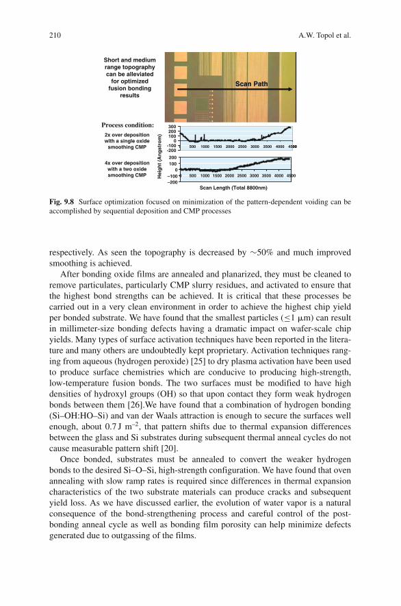
Chemical–mechanical polishing (CMP) is capable of smoothing a dielectric sur-face to <10 nm RMS per 30 �m2 roughness, with film thickness uniformity <5%3�, across a 200-mm Si wafer. Unfortunately, actual device wafers can pose uniquetopography issues if one measures over longer ranges (>30 �m). Topography intro-duced by CMP “dishing” effects introduced during BEOL damascene metal polishescan produce pattern-dependent voiding at the oxide fusion bond interface. Figure 9.7shows bonding voids produced between device-level probe pads when a blanketlow-temperature oxide (LTO) film is bonded over them. While it is possible tominimize the effect by careful consideration of pattern loading factors during themask design process, we have also found that a process-driven solution is also nec-essary. In particular, as shown in Fig. 9.8 some of the pattern-dependent topographycan be minimized by implementation of sequential PECVD oxide deposition andmultiple CMP processing steps. Figure 9.8 shows surface topography range for twoexamples in which 2x and 4x oxide was deposited over target “short” (<100-�m,probe pads) and “long” (>800-�m, full scan) pads with single or double CMP steps,
Pattern Specific Bonding VoidsPattern Specific Bonding VoidsPattern Specific Bonding VoidsPattern Specific Bonding Voids
Fig. 9.7 Example of pattern-dependent voiding at the oxide fusion bonding interface possiblecaused by the CMP “dishing” effects introduced during BEOL damascene metal polishes
210 A.W. Topol et al.
0100200
Scan PathScan Path
Short and medium range topography can be alleviated
for optimized fusion bonding
results
2x over deposition with a single oxide
smoothing CMP
4x over deposition with a two oxide smoothing CMP
-200-100
0100200300
0 500 1000 1500 2000 2500 3000 3500 4000 4500
Hei
gh
t (A
ng
stro
m)
Scan Length (Total 8800nm)
Process condition:
–200–100
Scan PathScan Path
500 1000 1500 2000 2500 3000 3500 4000 4500
0 500 1000 1500 2000 2500 3000 3500 4000 4500
Fig. 9.8 Surface optimization focused on minimization of the pattern-dependent voiding can beaccomplished by sequential deposition and CMP processes
respectively. As seen the topography is decreased by ∼50% and much improvedsmoothing is achieved.
After bonding oxide films are annealed and planarized, they must be cleaned toremove particulates, particularly CMP slurry residues, and activated to ensure thatthe highest bond strengths can be achieved. It is critical that these processes becarried out in a very clean environment in order to achieve the highest chip yieldper bonded substrate. We have found that the smallest particles (≤1 �m) can resultin millimeter-size bonding defects having a dramatic impact on wafer-scale chipyields. Many types of surface activation techniques have been reported in the litera-ture and many others are undoubtedly kept proprietary. Activation techniques rang-ing from aqueous (hydrogen peroxide) [25] to dry plasma activation have been usedto produce surface chemistries which are conducive to producing high-strength,low-temperature fusion bonds. The two surfaces must be modified to have highdensities of hydroxyl groups (OH) so that upon contact they form weak hydrogenbonds between them [26].We have found that a combination of hydrogen bonding(Si–OH:HO–Si) and van der Waals attraction is enough to secure the surfaces wellenough, about 0.7 J m–2, that pattern shifts due to thermal expansion differencesbetween the glass and Si substrates during subsequent thermal anneal cycles do notcause measurable pattern shift [20].
Once bonded, substrates must be annealed to convert the weaker hydrogenbonds to the desired Si–O–Si, high-strength configuration. We have found that ovenannealing with slow ramp rates is required since differences in thermal expansioncharacteristics of the two substrate materials can produce cracks and subsequentyield loss. As we have discussed earlier, the evolution of water vapor is a naturalconsequence of the bond-strengthening process and careful control of the post-bonding anneal cycle as well as bonding film porosity can help minimize defectsgenerated due to outgassing of the films.

9 3D Fabrication Options 211
Alignment
Since stacking of the devices has to occur on the device level the alignment toler-ance and interconnection geometry requirements are much more aggressive whencompared to any other 3D application. In particular since interconnecting vias withbottom diameter of ∼0.25 �m are typically expected to land on the pads designedwith about two times the tolerance; the tolerance for misalignment needs to becontrolled to <0.5 �m 3�. As discussed earlier, wafer-scale bonding alignmentscan be significantly affected by the physical characteristics of the substrates them-selves. For instance, we have shown that variations in substrate flatness, or bow,drive significant wafer-scale expansion errors [20]. We have also seen that localizedimperfections in bonding films or insufficient bonding oxide surface preparationcan drive lower (localized) bond energies and result in pattern overlay errors inthose areas. Another concern for wafer-scale bonding alignment is the effect ofbonding substrates which have been patterned independently on a variety of lithog-raphy steppers. Fortunately we have found that a variety of new process enhance-ments including wafer bow reduction, lithographic compensations and marking, useof glass carrier wafers, as well as new alignment test structure design have beendemonstrated to enable this tight alignment requirement [20, 27, 28].
Vertical Interconnect
The vertical interconnections in aggressive 3D IC applications need to meet thedensity requirement of the FEOL technology. To achieve this goal IBM has devel-oped 3D via technology. This via technology allows substantially denser 3D inter-connect pitch than is possible with TSVs, due to the limited aspect ratio of theTSV etch-and-fill technology. This 3D via approach builds upon BEOL metalliza-tion technology; the aspect ratio of vias (ratio of the height of via to its width)is enhanced, but typically not higher than 8:1. This rigorous specification can beachieved with a SOI-based layer transfer process which minimizes the 3D stackthickness. Figure 9.9 shows the structural comparison of TSVs [29] and 3D viatechnology [23], highlighting the difference in via geometry and pitches.
Final Metallization and Testing
Once interconnecting vias are processed the final metallization is based on the stan-dard BEOL technology. Depending on the application the number of metal lev-els may vary. Also additional metallization levels can be built before the stackingprocess. One has to only take into consideration the fact that interwafer vias havelimited aspect ratio and hence they can “go through” only so many layers. Bestdesigns are based on connecting the uppermost layer of the bottom wafer with thelowest metallization layers of the top wafer.
As always, testing of the stacked components is critical. Specialized test struc-tures can be designed not only to provide information regarding performance andreliability of interwafer connecting vias and bonding interface [24] but also to enable

212 A.W. Topol et al.
0.86•m
Size comparison of high density 3-D vias
with deep TSVs
Fig. 9.9 Comparison of TSVs from Tsang et al. (left) fabricated on bulk Si wafers to high-density3D vias from Topol et al. (right) fabricated using SOI-based 3D process
process optimization. For example, we have fabricated electrical and mechanicalstructures which were sensitive to via size (indicated minimum via size required)and provided layer-to-layer registration (alignment) information [28].
As we are progressing in qualifying 3D technology, verification test structuresfor circuit power and thermal management are becoming more critical. More specif-ically, to evaluate the thermal aspects of the 3D versus 2D ICs test structures basedon subthreshold slope and polysilicon resistance measurements have been imple-mented. In our work, we have designed and built structures that address both thespread-heating and self-heating issues of 3D stacking [18]. We have also designedand implemented, circuit performance integrity test structures, like ring oscillator(RO) structures, single transistors (FETs), and inverter circuit structures. Thesestructures help verify if thermal cycling and mechanical stresses, brought on bythe layer transfer processes during 3D IC fabrication, have an effect on overallperformance of the 3D structures. They also show if precise alignment and lowparasitic connection requirements have been met for stacking and interconnectingthe multiple layers [28].
9.2 Future Development Activities for 3D Integration
Clearly, in spite of great effort and work scope already covered in the area of 3Dintegration, several development activities must still be carried out in the fields ofsystem and device design and modeling, frontend processes, backend processes,manufacturing issues, electrical testing strategies, yield, and reliability.
9.2.1 Thermal Dissipation in Bonded Structures
Initial assessment of the impact of 3D layer transfer on circuit performance hasbeen reviewed [30]. However, additional evaluation of thermal dissipation in bondedstructures is critical. One aspect of the new 3D technologies that has to be addressed

9 3D Fabrication Options 213
is the thermal impact of the frontend and backend technology. Some of the issuesthat need to be investigated are self-heating effect on SOI wafers, Joule heatingin the backend (electrical resistance increases with T – nonlinear); low-� materials(thermal conductivity is a strong function of �); heat flow through the interconnect(complex geometry); and use of thermal vias and design rules to minimize tempera-ture rises (optimization). Joshi et al. [31] showed that simulation results clearly indi-cate the importance of the thermal effects in 3D integration structures. For example,the inclusion of Joule heating in the backend was found to be important. Therefore,detailed thermal analysis needs to be performed in early design stages, and it hasto include specific choice of materials used in 3D stacking. Also, layout issues anddesign rules need to be analyzed in the light of thermal impact.
9.2.2 Noise in 3D Integrated Structures
Newest efforts related to 3D modeling focus on better understanding of power sup-ply noise in 3D integrated systems [32, 33]. Simplified circuit models for powersupply delivery in 3D systems have been implemented analyzing the worst-casepeak noise for various layers. These calculations showed that in some cases a pro-hibitively large power supply noise can be reached and by adding P/G IOs, it canbe reduced to acceptable levels. The 3D power delivery problem has to be furtherevaluated to provide a high I/O design solution.
9.2.3 Bandwidth Utilization and Smart Power-Efficient Designs(Lower-Power Voltage Operations, Energy Efficiency)
9.2.3.1 Bandwidth Advantages of 3D
Perhaps the most compelling advantage of 3D integration for system applications isthe massive communication bandwidth that can be achieved between the chips in the3D stack. Figure 9.10 shows graphical representation of the 3D system performanceover the 2D solutions. The reason why this represents such an advantage for chipperformance can be understood by realizing that, in the last few years, the growthin microprocessor performance has been driven more by the utilization of multi-threaded, multicore architectures than by increasing clock frequencies. Such chiparchitectures, combined with specialized accelerator functions designed to furtherenhance chip performance, significantly increase the need for cache availability tosupport the many different threads running on a chip. In typical 2D chips, the fastcache memory is composed of SRAM or embedded DRAM (e-DRAM) [34] thatis integrated directly onto the chip. Three-dimensional integration enables greatertotal cache bandwidth in two ways. First, it allows the cache to be much larger,since in 3D, the amount of total chip area that can fit in a given footprint is greaterthat of a 2D chip. Secondly, and perhaps more importantly, 3D allows a much largernumber of interconnects to be made to the cache, since the cache can be integrated

214 A.W. Topol et al.
Sys
tem
Per
form
ance
Year
2D scalingregime
3D scalingregime
Future scalingtrend without 3D
Fig. 9.10 Comparison of system performance scaling trends for 2D and 3D solutions
vertically with respect to the logic portion of the chip, thereby eliminating the wiringblockages that limit that 2D intrachip interconnect densities. Due to the small lengthof these vertical interconnects (a few microns to a few tens of microns), much higherdata rates can be transmitted, at much lower power, compared to if they had to betransmitted across the chip, or off-chip.
9.2.4 Power-Efficient 3D Possibilities
Ultimately, the performance of many high-performance processors is limited by thetotal power that can be supplied to the chip, as well as the ability to dissipate theresulting heat. Given this constraint, one apparent way of improving the chip perfor-mance would be to increase the power efficiency of the logic function. For instance,greatly improved efficiency can be accomplished by reducing the supply voltage.For instance, reducing the supply voltage from 1 V to 0.5 V could increase the logicefficiency by a factor of close to 4x. Of course, this efficiency comes at the cost ofreduced processor speed, and must be made up for with parallelism if overall systemperformance is to be maintained. Such parallelism may be difficult to implement in2D systems, since the increase in silicon area would require multiple chips, andthe resulting power needed to drive the communications between the chips wouldnegate the advantages of the reduced supply voltages. However, in 3D architectures,the increased silicon area could be accommodated by stacking, while still maintain-ing low-power interconnection pathways, preserving the power advantages. In addi-tion, novel power-saving architecture strategies could be employed, such as utilizingSRAM or e-DRAM caches stacked in multiple layers above a dedicated logic core.Three-dimensional integration could provide elegant power management solutions,such as the utilization of voltage-regulation modules that could be implemented toprovide fine adjustment of the supply voltage to regions of the logic chip in order tocounterbalance local process variability, or provide fine-grain power management.

9 3D Fabrication Options 215
9.3 Summary
Motivations for 3D die stacking include reduction in system size, interconnect delay,and power dissipation, and enabling hyperintegration of chips fabricated usingdisparate process technologies. To enable 3D opportunities, IBM has developedfabrication technology based on both oxide- and Cu-bonding and has proven theviability of layer transfer processing to accomplish stacked 3D structures. We havefabricated, tested, and proven reliability of various metallization schemes enablinginterconnection between various stacked layers, which included TSV technologyand Cu-based IC interconnection technology. We have also pushed the alignmentslimits and shown that with an optimized process, alignment accuracy below 0.5 �mcan be achieved.
Going beyond the optimization of the fabrication process, IBM is currentlyfocused on remaining 3D technology challenges, which include heat analysis andremoval, understanding of modeling and design requirements for device and systemlevel, utilization of bandwidth provided by 3D with connection with smart low-power designs. We are designing and creating new test and reliability structures tomeasure noise immunity, heat dissipation, and system/circuit performance integrity.We are engaged in further modeling and design activities to take full advantage ofthe bandwidth benefits offered by 3D solutions and to create the future advancedCMOS-based 3D systems.
Acknowledgments The authors wish to thank for their contributions (1) the following IBM per-sonnel: Steven Steen, Kuan-neng Chen, Leathen Shi, Cornelia Tsang, Paul Andry, David Frank,Jyotica Patel, James Vichiconti, Deborah Neumayer, Narender Rana, Robert Trzcinski, LathaRamakrishnan, Roy Yu, James Tornello, Michael Lofaro, Gill Singco, John Ott, David DiMilia,William Price, Jesus Acevedo, and (2) the following RPI personnel: Dr. James Lu, Dr. Sang HwuiLee, Dr. Ravi Kumaroh. The authors also acknowledge the support of IBM’s MRL and CSS aswell as staff at EV Group and Suss MicroTec. This project was partially funded by DARPA undercontract numbers N66001-00-C-8003 and N66001-04-C-8032.
References
1. Moore G (1965) Cramming more components onto integrated circuits. Electronics 38(8):114–117
2. IBM press release (2007) IBM moves Moore’s law into the third-dimension http://www-03.ibm.com/press/us/en/pressrelease/21350.wss
3. Guarini K, Wong, H-SP (2004) Wafer bonding for high performance logic applications. In:Alexe M, Goesele U (eds) Wafer bonding: applications and technology. Springer-Verlag,Berlin, pp 157–160
4. http://www.techsearchinc.com/ (2007) In: Through Silicon Via Technology: The UltimateMarket for 3D Interconnect. TechSearch International Report
5. http://www.sematech.org/research/3D/6. Topol AW, Guarini KG, Yu R, Shi L, Newport MR, J. Tornello J, Melick D, O’Neil PA,
Colburn M, Singh DV, Cohen GM, Krishna M, Ruiz N, Pogge HB, Ieong M, PurushothamanS, Haensch WE (2003) Demonstration of wafer-level layer transfer of high performancedevices and circuits for three-dimensional integrated circuit fabrication. AVS 4th InternationalConference on Microelectronics and Interfaces, Santa Clara, CA, USA, pp 5–7

216 A.W. Topol et al.
7. Jonson SC (2007) 3-D TSV cips take off. Semiconductor International, July, p 408. Vardaman J (2007) 3-D Through-silicon vias become a reality. Semiconductor International,
June, pp 40–459. Andry PS, Tsang C, Sprogis E, Patel C, Wright SL, Webb BC (2006) A CMOS-compatible
process for fabricating electrical through-vias in silicon. Proceedings of the 56th ElectronicComponents and Technology Conference, San Diego, CA, pp 831–837
10. Tsang CK, Topol AW (2006) 3D integrated circuits and silicon carrier packaging realization.Proceedings of 23rd VLSI VMIC Conference, Fremont, CA, September 25–28, 2006, VMICno 06 IMIC-050 pp 61–69
11. Patel CS, Tsang CK, Schuster C, Doany FE, Nyikal H, Baks CW, Budd R,Buchwalter LP,Andry PS, Canaperi DF, Edelstein DC, Horton R, Knickerbocker JU, Krywanczyk T,Kwark YH, Kwietniak KT, Magerlein JH, Rosner J, Sprogis E (2005) Silicon carrier withdeep through vias, fine pitch wiring and through cavity for parallel optical transceiver. Pro-ceedings of the 55th Electronic Components and Technology Conf, Lake Buena Vista, FL,pp 1318–1324
12. Topol AW, Furman BK, Guarini KW, Leathen S, Cohen GM, Walker GF (2004) Enablingtechnologies for wafer-level bonding of 3D MEMS and integrated circuit structures. 54thElectronic Components and Technology Conference (ECTC), Las Vegas, NV; June 1–4, 2004;vol 1, no s21p2, pp 931–938
13. Chen KN, Tan CS, Fan A, Reif R (2004) Morphology and bond strength of copper waferbonding. Electrochem Solid-State Lett 7(1):G14–G16,
14. Chen KN, Tsang CK, Topol AW, Lee SH, Furman BK, Rath DL, Lu J-Q, Young AM,Purushothaman S, Haensch W (2006) Improved manufacturability of Cu bond pads andimplementation of seal design in 3D integrated circuits and packages. 23rd International VLSIMultilevel Interconnection (VMIC) Conference, Fremont CA, September 25–28, 2006, VMICCatalog No 06 IMIC-050, pp 195–202,
15. Chen KN, Lee SH, Andry PS, Tsang CK, Topol AW, Lin YM, Lu JQ, Young AM, Ieong M,Haensch W (2006) Structure design and process control for Cu bonded interconnects in 3Dintegrated circuits. International Electron Devices Meeting (IEDM) Technical Digest, Session13.5, pp 20–22
16. Ieong M, Narayana V, Singh D, Topol A, Chan V, Ren Z (2006) Transistor scaling with novelmaterials and integration. Mater Today 9(6):26–31
17. Ieong M, Guarini KW, Chan V, Bernstein K, Joshi R, Kedzierski J, Haensch W (2003) Threedimensional CMOS devices and integrated circuits. Proceedings of the IEEE Custom Inte-grated Circuits Conference, pp 207–213
18. Topol AW, La Tulipe DC, Shi L, Frank DJ, Bernstein K, Steen SE, Kumar A, Singco GU,Young AM, Guarini KW, Ieong M (2006) Three-dimensional integrated circuits. IBM J ResDev 50(4/5):491–506
19. Guarini KW, Topol KW, Ieong M, Yu R, Shi L, Newport MR, Frank DJ, Singh DV, Cohen GM,Nitta SV, Boyd DC, O’Neil PA, Tempest SL, Pogge HB, Purushothaman S, Haensch WE(2002) Electrical integrity of state-of-the-art 0.13 lm SOI CMOS devices and circuits trans-ferred for three-dimensional (3D) integrated circuit (IC) fabrication. IEDM Tech. Digest,pp 943–945
20. La Tulipe D, Shi L, Topol A, Steen S, Pfeiffer D, Posillico D, Neumayer D, Goma D,Vichiconti V, Rubino J, Young A, Ieong M (2006) Critical aspects of layer transfer andalignment tolerances for 3D integration processes. International Conference and Exhibition onDevice Packaging (IMAPS), Scottsdale, AZ, March 20–24, 2006, Journal of Microelectronicsand Electronic Packaging vol 3, no 1
21. Narayan C, Purushothaman S, Doany F, Deutsch A (1995) Thin film transfer process for lowcost MCM-fabrication. IEEE Transactions on Components, Packaging, and ManufacturingTechnology (Trans CPMT) Part B, vol 18, no 1, pp 42–46
22. Ultra Thin Wafer Processing Solutions. June 20, 2007, (http://www.semiconductor.net/web-castsDetail/2140049068.html). Semiconductor International Webcast

9 3D Fabrication Options 217
23. Topol AW, La Tulipe DC, Shi L, Alam SM, Frank DJ, Steen SE, Vichiconti J, Posillico D,Cobb M, Medd S, Patel J, Goma S, DiMilia D, Robson TM, Duch E, Farinelli M, Wang C,Conti RA, Canaperi DM, Deligianni L, Kumar A, Kwietniak KT, D’Emic C, Ott J, Young AM,Guarini KW, Ieong M (2005) Enabling SOI based assembly technology for three-dimensional(3D) integrated circuits (ICs). IEDM Tech. Digest, pp 363–366
24. Guarini KW, Topol TA, Singh DV, La Tulipe DC, Shi L, Young AM, Alam A, Frank DJ,Neumayer DA, Vichiconti J, Sicina RM, Conti RA, Wang C, Canaperi DM, Deligianni L,Kwietniak KT, Steen SE, Robson M, Gibson GW, Posillico D, Ieong M (2005) Processtechnologies for three dimensional integration. Proceedings of the 6th Annual InternationalConference on Microelectronics and Interfaces, American Vacuum Society, pp 212–214
25. Warner K, Burns J, Keast C, Kunz R, Lennon D, Loomis A, Mowers W, Yost D (2002) Low-temperature oxide-bonded three-dimensional integrated circuits. Proceedings of the IEEEInternational SOI Conference, Oct 7–10 2002, pp 123–125
26. Publications inclue: Tong QY et al (1996) Proceddings of the IEEE International SOI Con-ference, pp 36–37; Stengl R et al (1989) Jpn J Appl Phys 2810:1735–1741; Tong QY et al(1995) Electrochem Soc Proc 95(7):78–95
27. Steen SE, LaTulipe D, Topol A, Frank D, Belote K, Posillico D (2007) Wafer scale 3D inte-gration: overlay as key to drive potential. Microelec Eng 84(5–8):1412–1415, May–August2007
28. Topol AW, La Tulipe DC, Shi L, Alam SM, Young AM, Frank DJ, Steen SE,Vichiconti J, Posillico D, Canaperi DM, Medd S, Conti RA, Goma S, Dimilia D, Wang C,Deligianni L, Cobb MA, Jenkins K, Kumar A, Kwietniak KT, Robson M, Gibson GW,D’Emic C, Nowak E, Joshi R, Guarini KW, Ieong M (2005) Assembly technology for treedimensional integrated circuits. Proceedings of 22 nd International VLSI Multilevel Intercon-nection Conference (VMIC), a special conference of 2005 Institute for Microelectronics onChip Interconnection (IMIC), Fremont CA, Oct 4–6 2005, pp 83–88
29. Tsang CK, Andry PS, Sprogis EJ, Patel CS, Webb BC, Manzer DG, Knickerbocker JU (2006)CMOS-compatible through siIlicon vias for 3D process integration. Pannel Discussion onEnabling Technologies for 3D Integration; MRS Symposium Proceedings November 27–29,2006 Boston, MA, vol 970, pp 145–153
30. Guarini KW, Topol AT, Ieong M, Bernstein K, Xiu K, Joshi RV, Yu R, Shi L, Newport MR,Singh DV, Cohen GM, Pogge HB, Purushothaman S, Haensch WE (2003) The impact ofwafer-level layer transfer on high performance devices and circuits for 3D fabrication. Pro-ceedings of Electrochemical Society (ECS) Annual Meeting, Paris, France, Abstract #431,April 27–May 2, 2003, PV 2003-20, ISBN 1-56677-403-9, In: New Trends in Intercala-tion Compounds for Energy Storage Conversion (eds) Zaghib K, Julien CM, Prakash J,pp 390–404
31. Joshi RV, Smy T, Banerjee K, Topol A (2007) Thermal dissipation in bonded structures.In: Thermal and Design Issues in 3D ICs, SEMATECH Workshop, October 9–11, 2007, inAlbany, NY
32. Huang G, Bakir M, Naeemi A, Chen H, Meindl JD (2007) Power delivery for 3D chip stacks:physical modeling and design implication. IEEE 16th Conference on Electrical Performanceand Electronic Packaging, Atlanta, October 28–31 2007, Session IX, No 5
33. Huang G, Sekar D, Naeemi A, Shajeri K, Meindl JD (2007) Physical model for power supplynoise and chip/package co-design in Gigascale Systems with consideration of hot spots. IEEECustom Integrated Circuits Conference (CICC), San Jose, September 16–19 2007, no 27.1
34. Iyer S, Barth JE, Parries PC, Norum IP, Rice JP, Logan LR, Hoyniak D (2005) EmbeddedDRAM: technology platform for the blue gene/L chip. IBM J Res Dev 49(2–3):333–350