Wafer-Scale Functional Circuits Based on Two Dimensional ...
24
Wafer-Scale Functional Circuits Based on Two Dimensional Semiconductors with Fabrication Optimized by Machine Learning Xinyu Chen State Key Laboratory of ASIC and System, School of Microelectronics, Fudan University, Shanghai 200433 Yufeng Xie State Key Laboratory of ASIC and System, School of Microelectronics, Fudan University, Shanghai 200433 Yaochen Sheng Fudan University Hongwei Tang State Key Laboratory of ASIC and System, School of Microelectronics, Fudan University, Shanghai 200433 Zeming Wang State Key Laboratory of ASIC and System, School of Microelectronics, Fudan University, Shanghai 200433 Yu Wang State Key Laboratory of ASIC and System, School of Microelectronics, Fudan University, Shanghai 200433 Yin Wang State Key Laboratory of ASIC and System, School of Microelectronics, Fudan University, Shanghai 200433 Fuyou Liao State Key Laboratory of ASIC and System, School of Microelectronics, Fudan University, Shanghai 200433 Jingyi Ma State Key Laboratory of ASIC and System, School of Microelectronics, Fudan University, Shanghai 200433 Xiaojiao Guo School of Microelectronics, Fudan University Ling Tong State Key Laboratory of ASIC and System, School of Microelectronics, Fudan University, Shanghai 200433 https://orcid.org/0000-0002-8037-1340
Transcript of Wafer-Scale Functional Circuits Based on Two Dimensional ...

Wafer-Scale Functional Circuits Based on TwoDimensional Semiconductors with FabricationOptimized by Machine LearningXinyu Chen
State Key Laboratory of ASIC and System, School of Microelectronics, Fudan University, Shanghai200433Yufeng Xie
State Key Laboratory of ASIC and System, School of Microelectronics, Fudan University, Shanghai200433Yaochen Sheng
Fudan UniversityHongwei Tang
State Key Laboratory of ASIC and System, School of Microelectronics, Fudan University, Shanghai200433Zeming Wang
State Key Laboratory of ASIC and System, School of Microelectronics, Fudan University, Shanghai200433Yu Wang
State Key Laboratory of ASIC and System, School of Microelectronics, Fudan University, Shanghai200433Yin Wang
State Key Laboratory of ASIC and System, School of Microelectronics, Fudan University, Shanghai200433Fuyou Liao
State Key Laboratory of ASIC and System, School of Microelectronics, Fudan University, Shanghai200433Jingyi Ma
State Key Laboratory of ASIC and System, School of Microelectronics, Fudan University, Shanghai200433Xiaojiao Guo
School of Microelectronics, Fudan UniversityLing Tong
State Key Laboratory of ASIC and System, School of Microelectronics, Fudan University, Shanghai200433 https://orcid.org/0000-0002-8037-1340

Hanqi Liu State Key Laboratory of ASIC and System, School of Microelectronics, Fudan University, Shanghai
200433Hao Liu
Fudan UniversityTianxiang Wu
Fudan UniversityJiaxin Cao
State Key Laboratory of ASIC and System, School of Microelectronics, Fudan University, Shanghai200433Sitong Bu
State Key Laboratory of ASIC and System, School of Microelectronics, Fudan University, Shanghai200433Hui Shen
State Key Laboratory of ASIC and System, School of Microelectronics, Fudan University, Shanghai200433Fuyu Bai
State Key Laboratory of ASIC and System, School of Microelectronics, Fudan University, Shanghai200433Daming Huang
State Key Laboratory of ASIC and System, School of Microelectronics, Fudan University, Shanghai200433Jianan Deng
Fudan University https://orcid.org/0000-0001-7450-826XAntoine Riaud
State Key Laboratory of ASIC and System, School of Microelectronics, Fudan University, Shanghai200433Zihan Xu
Sixcarbon Tech. Shenzhen, Shenzhen 518106Chenjian Wu
School of Electronic and Information Engineering, Soochow University, Suzhou 215006Shiwei Xing
School of Electronic and Information Engineering, Soochow University, Suzhou 215006Ye Lu
State Key Laboratory of ASIC and System, School of Information Science and Technology, FudanUniversity, Shanghai 200433Shunli Ma
Fudan UniversityZhengzong Sun
Fudan UniversityZhongying Xue
Shanghai Institute of Microsystem and Information TechnologyZengfeng Di
Shanghai Institute of Microsystem and Information TechnologyXiao Gong
National University of SingaporeWei Zhang
Fudan UniversityPeng Zhou
Fudan University https://orcid.org/0000-0002-7301-1013Jing Wan
State Key Laboratory of ASIC and System, School of Information Science and Engineering, FudanUniversity, Shanghai 200433Wenzhong Bao ( [email protected] )
State Key Laboratory of ASIC and System, School of Microelectronics, Fudan University, Shanghai200433 https://orcid.org/0000-0002-3871-467X
Article
Keywords: devices, electronic materials, two-dimensional layered materials (2DLMs), machine-learning(ML)
Posted Date: January 27th, 2021
DOI: https://doi.org/10.21203/rs.3.rs-152918/v1
License: This work is licensed under a Creative Commons Attribution 4.0 International License. Read Full License
Version of Record: A version of this preprint was published at Nature Communications on October 12th,2021. See the published version at https://doi.org/10.1038/s41467-021-26230-x.
Wafer-Scale Functional Circuits Based on Two Dimensional
Semiconductors with Fabrication Optimized by Machine Learning
Xinyu Chen†1, Yufeng Xie†1, Yaochen Sheng†1, Hongwei Tang†1, Zeming Wang1, Yu
Wang1, Yin Wang1, Fuyou Liao1, Jingyi Ma1, Xiaojiao Guo1, Ling Tong1, Hanqi Liu1,
Hao Liu1, Tianxiang Wu1, Jiaxin Cao1, Sitong Bu1, Hui Shen1, Fuyu Bai1, Daming
Huang1, Jianan Deng2, Antoine Riaud1, Zihan Xu3, Chenjian Wu4, Shiwei Xing4, Ye
Lu2, Shunli Ma1, Zhengzong Sun1, Zhongyin Xue5, Zengfeng Di5, Xiao Gong6, David
Wei Zhang1, Peng Zhou*1, Jing Wan*2 and Wenzhong Bao*1
1 State Key Laboratory of ASIC and System, School of Microelectronics, Fudan
University, Shanghai 200433, P. R. China. 2 State Key Laboratory of ASIC and System, School of Information Science and
Technology, Fudan University, Shanghai 200433, P. R. China. 3 Shenzhen Six Carbon Technology, Shenzhen 518055, P. R. China. 4 School of Electronic and Information Engineering, Soochow University, Suzhou
215006, P. R. China. 5 State Key Laboratory of Functional Materials for Informatics, Shanghai Institute of
Microsystem and Information Technology, Chinese Academy of Sciences, 865
Changning Road, Shanghai, 200050, China 6 Department of Electrical and Computer Engineering, National University of
Singapore, Singapore 117583, Singapore.
*Correspondence to [email protected]; [email protected];
† These authors contribute to this work equally.
Abstract: Triggered by the pioneering research on graphene, the family of two-
dimensional layered materials (2DLMs) has been investigated for more than a decade,
and appealing functionalities have been demonstrated. However, there are still
challenges inhibiting high-quality growth and circuit-level integration, and results from
previous studies are still far from complying with industrial standards. Here, we
overcome these challenges by utilizing machine-learning (ML) algorithms to evaluate
key process parameters that impact the electrical characteristics of MoS2 top-gated
field-effect transistors (FETs). The wafer-scale fabrication processes are then guided
by ML combined with grid searching to co-optimize device performance, including
mobility, threshold voltage and subthreshold swing. A 62-level SPICE modeling was
implemented for MoS2 FETs and further used to construct functional digital, analog,
and photodetection circuits. Finally, we present wafer-scale test FET arrays and a 4-bit
full adder employing industry-standard design flows and processes. Taken together,
these results experimentally validate the application potential of ML-assisted
fabrication optimization for beyond-silicon electronic materials.

Two-dimensional layered materials (2DLMs) have potential applications from
mainstream logic and analog circuits to flexible electronics 1-8. Semiconductive
transition metal dichalcogenides (TMDs) are a family of 2DLMs with versatile band
structures, among which MoS2 is the most widely studied representative of TMDs 9-18.
The atomically thin channel with dangling-bond-free interfaces and low in-plane
dielectric constants ensure high carrier mobility in extremely scaled devices with robust
control over short-channel effects (SCEs) 19-21. While intrinsic advantages of 2DLMs
are promising for More-than-Moore electronic applications 22-25, it is still difficult to
meet the stringent requirements for large-scale circuit- and system-level applications,
where the primary challenges are wafer-scale material synthesis and device processing
26-29. Recent progress in chemical vapor deposition (CVD)/metal-organic chemical
vapor deposition (MOCVD) growth has enabled semiconductive TMD films with large
areas 30-32. Although satisfied crystalline quality and large-scale uniformity still require
further improvement of synthesis techniques, currently available wafer-scale TMD
films are practically sufficient for fabricating large-scale circuits.
In order to realize complex cascaded circuits, voltage level matching and high
noise margins are also important 33, placing the need for the accurate control of
threshold voltage VT. So far, a circuit based on MoS2 consisting of 115 field-effect
transistors (FETs) with gate-first technology has been reported 33,34. However,
compared to conventional gate-last processing 35, gate-first technology requires a more
complex film transfer processing and an extra step of via etching, which not only
introduces defects to MoS2 films but also drastically reduces yield and reproducibility
of wafer-scale fabrication. Hence, large-scale 2DLM based circuits require more
emphasis on fabrication optimization towards wafer-scale uniformity and
reproducibility.
In this work, to realize batch fabrication using 2 in. MoS2 wafer, machine-learning
(ML) algorithms were used to analyze experimental data and evaluate various key
process parameters that significantly impact the electrical characteristics of 2D-FETs,
enabling optimized electrical performance for enhancement-mode FETs fabricated

using ML-guided gate-last processing. Calibrated by measured electrical data, the
device modeling is conducted to guide the design of basic digital, analog, and
optoelectrical circuits. With wafer-scale processing using industry-standard design
flows and processes, our work illustrates the feasibility of using ML in device
processing optimization for emerging novel materials and shortens the learning cycle
from fundamental research to practical application.
High quality, uniform MoS2 was grown using customized CVD equipment (see SI
for details). Raman mapping results indicate the synthesized wafer is uniform at the
wafer-scale, as shown in Fig. 1a (see Fig S1 for more details). Although the growth of
wafer-scale MoS2 films has been demonstrated 30-32, fabrication of MoS2 FETs still
requires optimizing individual process modules, such as channel doping, S/D contact,
and gate stack interface. These process steps are strongly correlated to the final device
performance metrics, including carrier mobility (μ), threshold voltage (VT), and
subthreshold swing (SS), as shown in Fig. 1c. For practical applications, it is necessary
to optimize the combination of these quantities, and different applications of the device
also require different optimization strategies, as illustrated in Fig. 1b. Due to the
extremely high sensitivity of channel carriers to the ambient environment, multiple
processing steps impact various aspects of electrical performance, making
comprehensive process optimization complicated and challenging. After optimizing
wafer-scale material and device fabrication processes, we continue to carry out device
characterization, SPICE modeling, and circuit design. The obtained device and circuit
characterization results can also be further used to guide improvements to the
fabrication process, as illustrated by Fig. 1d.
The fast-developed ML technology is commonly used for the efficient
understanding of complex mathematical or logical models. ML has been used in many
disciplines, such as the exploration of novel materials 36, but there has never been any
report on using ML to optimize process modules for 2D devices. Here, we show that
ML can improve the fabrication process of devices built on emerging semiconductors
more effectively than the conventional process optimization method. Specifically, ML

is used to understand the impact of each processing step on the final device performance.
This is essential for materials, such as MoS2 grown via CVD, which are synthesized on
an insulating substrate, making device measurements after each processing step
difficult.
A complete process for fabricating MoS2 top-gate FETs (TG-FETs) is shown in
Fig. 2a. The FET performance is measured at the end of the process flow. Ensemble
learning (EL), a supervised ML method where multiple learning algorithms are
aggregated for more accurate prediction 37, is used here as it is effective for classifying
imbalanced data (see SI for more details). The decision tree method is used as a weak
classifier because it can efficiently handle discrete data (Fig. 2b). More than 560 MoS2-
FETs on over 40 different wafers were fabricated using specially designed process
flows to provide a comprehensive database. We first focus on two device performance
parameters, μ and VT, as μ is directly correlated to operation speed and VT is essential
for fabricating an enhancement mode FET. The importance of each processing step can
be determined using only one parameter (μ or VT) as the sorting standard for EL analysis
(see Fig. 2c and Table S1 for detailed processing steps). The generated results are
reasonable since VT is primarily influenced by the top gate structure (metal work
function and charge impurities/dipoles in the deposited gate dielectric), while μ depends
on more factors, including the contact resistance and charge scattering. The TG
electrode metallization also becomes an essential step as indicated by ML analysis,
which is unexpected (details see Fig. S6). μ, VT, and other performance parameters can
be comprehensively considered by multiplying a weighting factor for each parameter,
depending on the requirements of various functionalities (also see SI).
ML can also be used to co-optimize all process parameters, as shown in Fig. 2d.
After EL training, a score predictor can be used to predict the results from any processing
combination. All possible processing combinations are then sorted using a grid search
method, as shown in Fig. 2e. To demonstrate this, we chose more than 500 devices,
which are summarized in the μ-VT plot in Fig. 2f. While one recipe provides a high μ
value (red stars), another recipe provides a positive VT value. However, both values

decrease when the two recipes are combined, which is mainly due to crosstalk between
different processing steps. Therefore, the combination of multiple steps with each
optimized recipe does not necessarily generate an optimized device. By following the
suggestion of this sorting result, seven devices with better performance were
successfully fabricated (red stars in Fig. 2f). This recipe combination (details see
Supplementary Table 6) also gives rise to an average μ about 75 cm2/V∙s and Vth about
2.1 V, as well as a high wafer-scale uniformity that is important for large scale circuits,
as shown in Fig. 2g. The application of the ML algorithm in MoS2 device optimization
is only a case study, and its capability to speed up the learning cycle for performance
optimization of devices with multiple processes can be conveniently extended to other
2DLMs and emerging electronic materials.
Since the FETs built on the wafer have high uniformity, we use an RPI model (level
= 62) to simulate MoS2 FETs in an HSPICE simulator. As is shown in Fig. 3a-b, to fit
the transfer and output characteristics of MoS2 FETs, the parameters of the model are
configured by adjusting the empirical parameters and characteristic parameters (such as
mobility and VT extracted from transfer curves; thickness and permittivity of the
dielectric; W and L of MoS2 channel). The voltage transfer characteristics (VTC) for a
pseudo-NMOS type MoS2 inverter (M1 as a load transistor and M2 as a pull-down
network) were also simulated in HSPICE using the simulation parameters from the same
model. By sizing the aspect ratio W/L of two MoS2 FETs (Fig. 3c) and shifting the VT
value (Fig. 3d) of the M1 independently, the voltage switching point can be tuned to the
proper position (around half of VDD) to achieve rail-to-rail output swing and large noise
margin (see Fig. S10 for more details).
A flip-flop is a fundamental storage element for sequential ICs 38-41. Fig. 3e shows
a circuit schematic and a die photo of a negative edge triggered D flip-flop (DFF) based
on 8 NANDs with 2 inputs and 3 inverters. The measured waveforms from the DFF are
plotted in Fig. 3f, where the device outputs correct logic values for given input data on
the falling edge of the clock (CLK) and holds the data until the next falling edge. A full
adder is another key combinational circuit usually used as a fundamental building block

in an arithmetic logic unit (ALU) 33,42. Fig. 3g shows a circuit schematic of a 1-bit full-
adder and a photograph of the die. The 1-bit full-adder consists of 10 NANDs, 3 inverters,
and 1 NOR with 39 n-FETs in total. The measured output waveforms from the 1-bit full-
adder are shown in the bottom plots of Fig. 3h, where the outputs (“S” and “Co”) produce
the correct rail-to-rail voltage for all possible input combinations with 3.0 V supply
voltage.
A ring oscillator (RO) is an industrial standard benchmarking circuit for
performance evaluation 42,43. We then fabricated and measured a 5-stage pseudo-CMOS
RO with an output buffer (Fig. 3i) to assess the high frequency switching capability of
MoS2. Such RO circuit is composed of five inverters cascaded in a loop chain. High
uniformity of all inverter stages, such as their large noise margin, is essential for robust
oscillator performance. As shown in Fig. 3j, an oscillation frequency of 19.5 kHz with a
propagation delay of 𝜏𝑝𝑑 = 1/(2𝑛𝑓) = 5.13 𝜇𝑠 per stage was measured at VDD = 3 V,
where n is the number of stages. In the future, various methods could be applied to
increase the oscillation frequency, which is correlated to gate parasitic capacitance, drive
current, and supply voltage.
For memory applications, we present dynamic memory arrays built from MoS2
FETs (Fig. 3k). A schematic diagram of a 1T-1C circuit is shown in Fig. 3l. An
oscilloscope was used to test its function as memory (Fig S14) 44-48. The experimental
results are shown in Fig. 3m. During a write operation, the MoS2 FET is turned on to
provide a low-impedance path, and a positive current pulse (red curve) is collected by
the oscilloscope, which indicates the capacitance has been recharged. During the holding
state, the MoS2 FET is turned off and presents a high-impedance path. If the current
pulse detected by the oscilloscope is negative during a read operation, it indicates that a
charge remains in the capacitor after the hold time. Due to the ultralow leakage current
from our MoS2 FET, the charge saved in the capacitor is expected to be ideally stored,
thereby achieving long-term retention. By integrating the current pulse during a read
operation, we can estimate the charge retained in the capacitor as a function of hold time,
as shown in Fig. 3n. The retention time is defined as the hold time at which the retained

charge (Qread) is zero compared with a read voltage of 0.5 V; the average retention time
is on the order of seconds.
Furthermore, our wafer-scale MoS2 devices can be extended for optoelectrical
application49. A thin layer Au (~10nm) deposited as TG electrode will have higher
optical transmittance, as shown in Fig. 3o. The transfer characteristics (Fig. 3p) from a
typical device show a considerable photocurrent of ~1 μA/μm under white light (1.5
mW/cm-2 ) when VTG = 4 V and an on-off ratio of approximately 100 when VTG = 0 V.
In Fig. 3q, we use a 9×9 MoS2 FET array to demonstrate a simple function of image
sensing. The photocurrents are recorded from each pixel by scanning a focused white
beam across the array. We set the illumination position to form the English letters F, D
and U deliberately. The color pattern representing the photocurrent value exhibits high
On/Off contrast and high spatial uniformity.
Here we have demonstrated logic, analog, memory, and optoelectronic functions,
which can be conveniently integrated into a single device. In the future, if we further
take advantage of the atomically thin and flexible nature of 2D materials, it is possible
to prepare three-dimensional monolithic integrated circuits (3D integration) by stacking
2DLMs with different functions 50. Thus, it provides a new route to implement a complex
system to realize various applications.
To demonstrate the potential for high volume production, we fabricated MoS2 TG-
FET arrays and 1-bit full-adder arrays on a 2-inch wafer, as shown in Fig. 4a. Similar to
what is normally completed in a semiconductor fabrication facility, the full-adder arrays
were placed in the center region of the wafer as a functional block, and MoS2 TG-FETs
were placed surrounding the functional blocks and used to monitor wafer-scale
uniformity. Each block contained 16 FETs, and 81 blocks in total were distributed across
the wafer. The average mobility and VT values extracted from the transfer curves in each
FET array are plotted in Fig. 4b, showing a wafer-scale uniformity acceptable for batch
fabrication. The average mobility and VT values for all 1296 MoS2 FETs are 46.7 cm2
V−1 s−1 and 1.9 V, respectively, with a standard deviation < 30%. In the rest of the wafer
area, we tested 144 1-bit full-adder circuits, revealing 50% yield (right graph of Fig. 4b).
This indicates our wafer-scale MoS2 film together with device processing have the
potential to achieve industrial high-volume production. To the best of our knowledge,
these are among the highest mobility and VT values observed in wafer-scale-fabricated
MoS2 TG devices with high uniformity (Supplementary Table 7). Finally, we fabricated
a 4-bit full-adder composed of four parallel 1-bit full-adders consisting of 156 FETs; the
microscope image and truth table are shown in Fig. 4c. The 4-bit full-adder was tested
using 8 input signal combinations (A3 A2 A1 A0, B3 B2 B1 B0, Ci), including (0000,
0000, 0), (0000, 0111, 0), (1111, 1000, 0), (1111, 1111, 0), (0000, 0000, 1), (0000, 0111,
1), (1111, 1000, 1), and (1111, 1111, 1). The output results in Fig. 4d show that the 4-
bit full-adder exhibits correct logical function and rail-to-rail conversion. Thanks to the
machine learning optimized fabrication process, we demonstrated the first complete 4-
bit full-adder based on MoS2 TG-FETs, paving the way to constructing future large-
scale 2D integrated circuits.
Conclusion
In this work, based on a wafer-scale MoS2 film, we integrated ML algorithms to
analyze experimental data for extracting key process parameters to optimize device
performance. Following this strategy, we successfully fabricated enhancement-mode
MoS2 TG-FETs using ML-guided gate-last processing recipes, and the corresponding
62-level SPICE modeling was also built. Basic logic, analog, and optoelectrical circuits
were constructed. Finally, wafer-scale device fabrication and measurements using
industry-standard design flow and processing were performed. Our results show that
ML can be used for device optimization and shortening the learning cycle for novel
materials. We also show that our MoS2 TG-FET technology is a potential route for
fabricating large-scale integrated circuits compatible with current silicon-based
technologies, and will promote the future application of 2D materials in large scale
integrated circuits.
Methods
Synthesis of wafer-scale MoS2. A crucible with MoO3 power (Alfa Aesar 99.95%) is
placed in Zone 2 while an appropriate amount of sulfur powder (Alfa Aesar 99.999%)

is placed in Zone 1 which is upstream of the flow in the tube. The distance between two
zones is 30 cm. A carefully rinsed sapphire substrate is placed face-down on the MoO3
power. During the synthesis process, 300 sccm argon gas serves as carrier gas. The
synthesis temperature for Zone 1 and Zone 2 is controlled at 180 oC and 650 oC,
respectively. Continuous monolayer MoS2 film is synthesized at atmospheric pressure
with 10 min sulfuration time.
Fabrication of MoS2 FETs and circuits. The MoS2 FETs and circuits are fabricated
on the wafer-scale MoS2 film on the sapphire substrate. The contact electrodes, source
and drain contacts, are patterned by laser direct writing technology (Micro-Writer ML3)
and subsequently deposited using Electronic Beam (E-beam) evaporation. CF4 plasma
etching is performed to define MoS2 channel region. A seeding layer is deposited by E-
beam evaporation and subsequently annealed in an oxygen atmosphere at 100 ℃. Then
HfO2 is then grown by Atom Layer Deposition (ALD) as the FET dielectric layer.
Another lithography/lift-off/deposition process is utilized to form the top metal layer.
For electrical probing or further fabrication of more complex circuits, SF6 plasma
etching is used to remove the HfO2 layer on top of the source/drain electrodes to form
via holes defined by the lithography.
The machine learning method. The details of ensemble learning, random forest
algorithm and feature importance assessment are described in the supplementary
information
Electrical measurement. The electrical properties of MoS2 FETs and circuits are
carried out in a probe station connecting to an Agilent B1500A semiconductor analyzer
with 8 source measure units. To investigate the circuit’s dynamic response, an Agilent
33622A arbitrary waveform generator is used to input signals while a RIGOL DS1054Z
digital oscilloscope captures the output voltage.
Data availability. The data that support the findings of this study are available from
the corresponding author on request.
Acknowledgments

We thank Prof. He Tian for the insightful discussion. This research is supported in part
by the National Key Research and Development Program (2016YFA0203900),
Shanghai Municipal Science and Technology Commission (18JC1410300), Shanghai
Rising Star Program (19QA1401100), and National Natural Science Foundation of
China (61925402, 51802041, 51925208, 61904032, 61874154, 61874031).
Author contributions: W.B., J.W. P.Z were in charge, advised, and led on all aspects
of the project. Y.X., Z.W. and Y.W. developed the ML algorithms. X.C., Y.S., H.T.,
Y.X., T.W., C.W., S.X. and S.M. contributed to circuit design. X.C., Y.S., H.T., Y.W.,
F.L., J.M., X.G. and L.T. fabricated the devices and circuits. X.C., H.T., Y.W., S.B,
H.S., F.B. and D.H. contributed to the electrical measurements. Z. X., Z.S., Z.X. and
Z.D. prepared the 2DLM materials. Y.L., X.G, J.W. advised industrial wafer-scale
circuit design and test. All authors discussed the results and commented on the
manuscript.
Competing interests: The authors declare no competing financial interests.

References:
1 Li, N. et al. Large-scale flexible and transparent electronics based on monolayer
molybdenum disulfide field-effect transistors. Nature Electronics 3, 711-717
(2020).
2 Liu, F. et al. Disassembling 2D van der Waals crystals into macroscopic
monolayers and reassembling into artificial lattices. Science 367, 903 (2020).
3 Zhang, Z. et al. Robust epitaxial growth of two-dimensional heterostructures,
multiheterostructures, and superlattices. Science 357, 788 (2017).
4 Li, J. et al. General synthesis of two-dimensional van der Waals heterostructure
arrays. Nature 579, 368-374 (2020).
5 Pospischil, A. et al. CMOS-compatible graphene photodetector covering all
optical communication bands. Nature Photonics 7, 892-896 (2013).
6 Yang, Y. et al. Large-area graphene-nanomesh/carbon-nanotube hybrid
membranes for ionic and molecular nanofiltration. Science 364, 1057 (2019).
7 Mennel, L. et al. Ultrafast machine vision with 2D material neural network
image sensors. Nature 579, 62-66 (2020).
8 Liu, Y. et al. Van der Waals heterostructures and devices. Nature Reviews
Materials 1, 16042 (2016).
9 Nourbakhsh, A. et al. in 2015 Symposium on VLSI Technology (VLSI
Technology). T28-T29.
10 Wang, H. et al. in International Electron Devices Meeting. 4.6.1-4.6.4.
11 Wang, H. et al. Integrated Circuits Based on Bilayer MoS2 Transistors. Nano
Letters 12, 4674-4680 (2012).
12 Yu, L. et al. in International Electron Devices Meeting. 32.33.31-32.33.34.
13 Liu, Y. et al. Approaching the Schottky–Mott limit in van der Waals metal–semiconductor junctions. Nature 557, 696-700 (2018).
14 Polyushkin, D. K. et al. Analogue two-dimensional semiconductor electronics.
Nature Electronics 3, 486-491 (2020).
15 Mennel, L. et al. Optical imaging of strain in two-dimensional crystals. Nature
Communications 9, 516 (2018).
16 Yu, W. J. et al. Highly efficient gate-tunable photocurrent generation in vertical
heterostructures of layered materials. Nature Nanotechnology 8, 952-958
(2013).
17 Manzeli, S., Ovchinnikov, D., Pasquier, D., Yazyev, O. V. & Kis, A. 2D
transition metal dichalcogenides. Nature Reviews Materials 2, 17033 (2017).
18 Ciarrocchi, A., Avsar, A., Ovchinnikov, D. & Kis, A. Thickness-modulated
metal-to-semiconductor transformation in a transition metal dichalcogenide.
Nature Communications 9, 919 (2018).
19 Liu, H., Neal, A. T. & Ye, P. D. Channel Length Scaling of MoS2 MOSFETs.
ACS Nano 6, 8563-8569 (2012).
20 Desai, S. B. et al. MoS2 transistors with 1-nanometer gate lengths. Science 354,
99 (2016).
21 Wang, L. et al. Electronic Devices and Circuits Based on Wafer-Scale
Polycrystalline Monolayer MoS2 by Chemical Vapor Deposition. Advanced
Electronic Materials 5, 1900393 (2019).
22 Fiori, G. et al. Electronics based on two-dimensional materials. Nature
Nanotechnology 9, 768-779 (2014).
23 Nikonov, D. E. & Young, I. A. Overview of Beyond-CMOS Devices and a
Uniform Methodology for Their Benchmarking. Proceedings of the IEEE 101,
2498-2533 (2013).
24 Akinwande, D. et al. Graphene and two-dimensional materials for silicon
technology. Nature 573, 507-518 (2019).
25 Liu, C. et al. Two-dimensional materials for next-generation computing
technologies. Nature Nanotechnology 15, 545-557 (2020).
26 Radisavljevic, B., Whitwick, M. B. & Kis, A. Integrated Circuits and Logic
Operations Based on Single-Layer MoS2. ACS Nano 5, 9934-9938 (2011).
27 Wang, H. et al. in 2012 International Electron Devices Meeting. 4.6.1-4.6.4.
28 Wang, Q. H., Kalantar-Zadeh, K., Kis, A., Coleman, J. N. & Strano, M. S.
Electronics and optoelectronics of two-dimensional transition metal
dichalcogenides. Nature Nanotechnology 7, 699-712 (2012).
29 Chen, J. et al. Building two-dimensional materials one row at a time: Avoiding
the nucleation barrier. Science 362, 1135 (2018).
30 Zhan, Y., Liu, Z., Najmaei, S., Ajayan, P. M. & Lou, J. Large-Area Vapor-Phase
Growth and Characterization of MoS2 Atomic Layers on a SiO2 Substrate. Small
8, 966-971 (2012).
31 Dumcenco, D. et al. Large-Area Epitaxial Monolayer MoS2. ACS Nano 9, 4611-
4620 (2015).
32 Kang, K. et al. High-mobility three-atom-thick semiconducting films with
wafer-scale homogeneity. Nature 520, 656-660 (2015).
33 Wachter, S., Polyushkin, D. K., Bethge, O. & Mueller, T. A microprocessor
based on a two-dimensional semiconductor. Nature Communications 8, 14948
(2017).
34 Yu, L. et al. Design, Modeling, and Fabrication of Chemical Vapor Deposition
Grown MoS2 Circuits with E-Mode FETs for Large-Area Electronics. Nano
Letters 16, 6349-6356 (2016).
35 Xu, H. et al. High-Performance Wafer-Scale MoS2 Transistors toward Practical
Application. Small 14, 1803465 (2018).
36 Butler, K. T., Davies, D. W., Cartwright, H., Isayev, O. & Walsh, A. Machine
learning for molecular and materials science. Nature 559, 547-555 (2018).
37 Liu, Y. & Yao, X. Ensemble learning via negative correlation. Neural Networks
12, 1399-1404 (1999).
38 Partovi, H. et al. in 1996 IEEE International Solid-State Circuits Conference.
Digest of TEchnical Papers, ISSCC. 138-139.
39 Sun, D.-m. et al. Flexible high-performance carbon nanotube integrated circuits.
Nature Nanotechnology 6, 156-161 (2011).

40 Yang, Y., Ding, L., Han, J., Zhang, Z. & Peng, L.-M. High-Performance
Complementary Transistors and Medium-Scale Integrated Circuits Based on
Carbon Nanotube Thin Films. ACS Nano 11, 4124-4132 (2017).
41 Lei, T. et al. Low-voltage high-performance flexible digital and analog circuits
based on ultrahigh-purity semiconducting carbon nanotubes. Nature
Communications 10, 2161 (2019).
42 Chen, B. et al. Highly Uniform Carbon Nanotube Field-Effect Transistors and
Medium Scale Integrated Circuits. Nano Letters 16, 5120-5128 (2016).
43 Zhang, H. et al. High-Performance Carbon Nanotube Complementary
Electronics and Integrated Sensor Systems on Ultrathin Plastic Foil. ACS Nano
12, 2773-2779 (2018).
44 Bertolazzi, S., Krasnozhon, D. & Kis, A. Nonvolatile Memory Cells Based on
MoS2/Graphene Heterostructures. ACS Nano 7, 3246-3252 (2013).
45 Liu, C. et al. A semi-floating gate memory based on van der Waals
heterostructures for quasi-non-volatile applications. Nature Nanotechnology 13,
404-410 (2018).
46 Xiang, D. et al. Two-dimensional multibit optoelectronic memory with
broadband spectrum distinction. Nature Communications 9, 2966 (2018).
47 Liu, C. et al. Small footprint transistor architecture for photoswitching logic and
in situ memory. Nature Nanotechnology 14, 662-667 (2019).
48 Migliato Marega, G. et al. Logic-in-memory based on an atomically thin
semiconductor. Nature 587, 72-77 (2020).
49 Lopez-Sanchez, O., Lembke, D., Kayci, M., Radenovic, A. & Kis, A.
Ultrasensitive photodetectors based on monolayer MoS2. Nature
Nanotechnology 8, 497-501 (2013).
50 Jiang, J., Parto, K., Cao, W. & Banerjee, K. Ultimate Monolithic-3D Integration
With 2D Materials: Rationale, Prospects, and Challenges. IEEE Journal of the
Electron Devices Society 7, 878-887 (2019).

Fig. 1. a, Demonstration of uniform wafer-scale MoS2 growth by CVD, including a schematic
diagram of the material growth equipment, a batch of 2 in. wafer-scale sapphire substrates
uniformly covered with MoS2, a 2 in. sapphire wafer uniformly covered with MoS2 marked
with Raman test points, and Raman mapping spectra from different locations marked in the
previous picture. b, Schematic cross-section of an MoS2 FET with TG and global BG. Various
factors that influence the device performance are categorized. c, Schematic diagram of the
relationship between performance parameters of the transistor and performance limitations of
the integrated circuit. d, Process flow and feedback optimization diagram from material
synthesis to industrial-grade circuit design, fabrication, and test.
Figure 1
Material synthesis
Fermi-pinning
Seeding LayerMoS2
MoS2
+
HfO2Dangling
bonds
Metal HfO2
Top dielectric
Si
Back dielectric
Top Gate
S D
2D-FET
Seedinglayer
HfO2
- +
- +
- +
Metal
Fermi-pinning
MoS2+
+
- +Dipoles
Defects- +
Traps
Adsorbates
μ Vth
Ion/Ioff SS
Speed
Power
consumption
Integration
a b
c
FET fabrication
Performance and
reliability test
SPICE model
MoS2 IC design
IC Fabrication
IC test
Guide of optimization
Material synthesis
Guide of optimization
Gate/high-k SL/high-k
2D/high-k2D/Contact Metal
d

Fig. 2. a, Process flow for fabricating TG MoS2 FETs. The variations in each step are marked
in blue. The end shows a three-dimensional hierarchical structure of an integrated circuit built
with gate-last technology. b, Graphical representation of ensemble learning based on decision
tree algorithm. The importance of each processing step is extracted during the creation of
decision trees. c, Importance of processing steps for μ and VT based on random forest regression.
d, Fabrication co-optimization based on ML. After training with EL, a score predictor can
predict the overall device performance for all processing combinations using a grid search
method. e, Ranking of all possible processing combinations. The high score combinations can
be referenced for device fabrication. f, More than 500 MoS2 TG-FETs summarized in a μ-VT
plot. Each color corresponds to one type of processing flow, and the red stars are devices
fabricated with the guidance of ML analysis. g, Transfer characteristics for 60 MoS2 TG-FETs
on one wafer at VDS = 0.5 V in linear and logarithmic coordinates. The inserts show histograms
and Gaussian fits of statistical data for Y-function calculated mobility (upper) and threshold
voltage (downside) to Gaussians.
Figure 2
0 100 200 300 400 5000
20
40
60
80
Eva
luati
on
Sco
re
Process Combination #
Imp
rota
nc
e(a
.u.)
0.01
0.02
0.03
0 10 20 30 40 50
0.01
0.02
0.03
Process step #
MoS2 Growth S/D SLc TG
-3 -2 -1 0 1 2 3 410
-14
10-12
10-10
10-8
10-6
10-4
I D(
A/
m)
I D(A
/m
)
VTG
(V)
0
2
4
6
8
b d f
g
1.2 1.6 2.0 2.40
20
40
VT(V)
-5 -4 -3 -2 -1 0 1 2 30
20
40
60
80
100
120
VT (V)
(cm
2/V
•s)
%
%
%
%
%
%Annealing(varying temperature)
Top gate electrical measurement
Top gate metallization (varying metals & evaporation tools)
MoS2 deposition (2-3 nm)
Patterning of S/D contacts
(E-beam or photo-lithography, varying lithography recipes)
S/D contacts metallization(varying metals & evaporation tools)
ALD HfO2
(varying temperature)
a
Seeding layer deposition (varying seeding materials & thickness)
Annealing (varying gas flow conditions & temperature )
Importance measure of each Processing step
…
Tree 1 Tree 2
Tree 3 Tree 4
Ensemble training based
on >560 2D-FETs
Voter
e
0
20
40
Mobility(cm2/(Vs))
30 50 70 90 100
Ranking of all combinations
Processing Step 3
Grid search
Recipe 1
Recipe 2
Processing Step 1 …
…
Recipe 1
Recipe 2
Recipe 35
12
com
bin
atio
ns
Recipe 3
Recipe 4
Processing Step 2
Recipe 1
Recipe 2
Score predictor
Ensemble training
Mobility favored
Vth favored
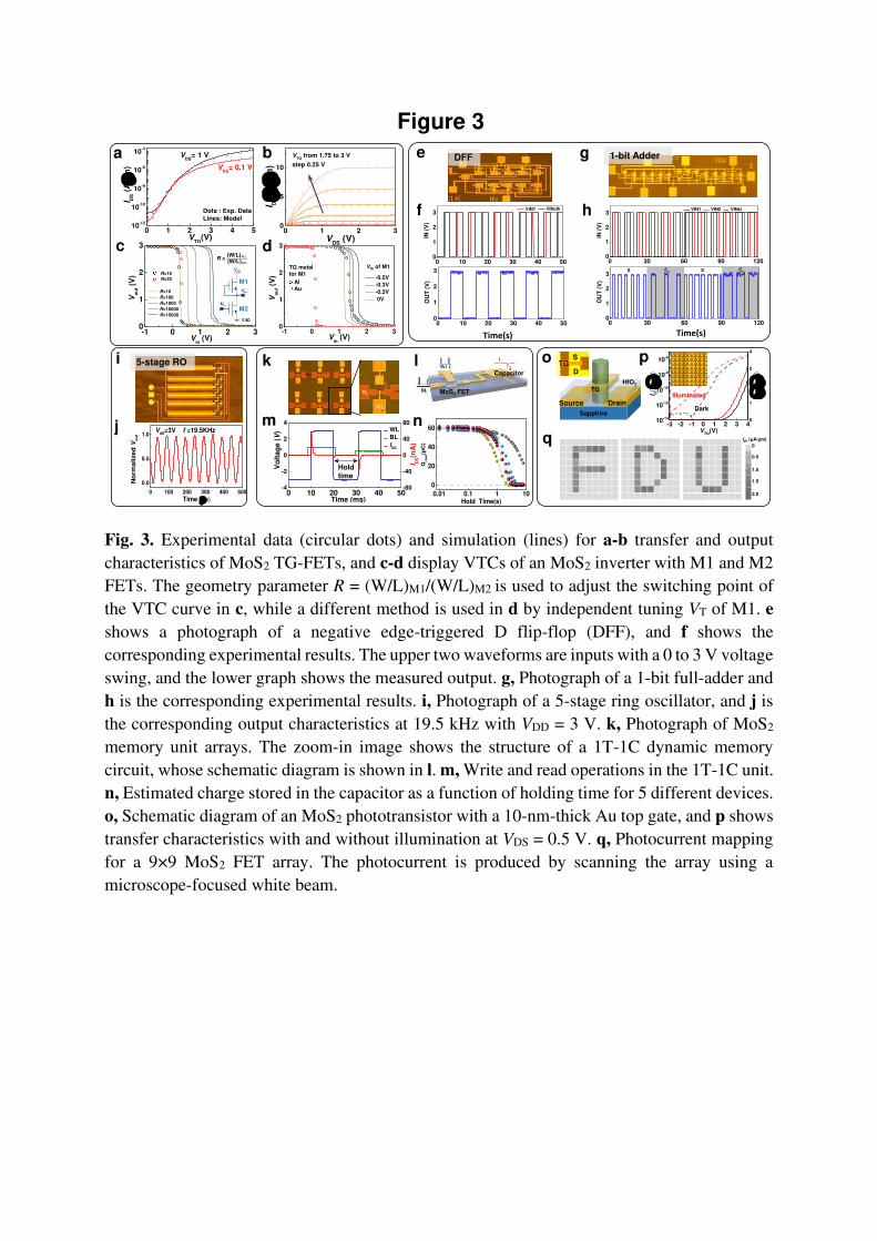
Fig. 3. Experimental data (circular dots) and simulation (lines) for a-b transfer and output
characteristics of MoS2 TG-FETs, and c-d display VTCs of an MoS2 inverter with M1 and M2
FETs. The geometry parameter R = (W/L)M1/(W/L)M2 is used to adjust the switching point of
the VTC curve in c, while a different method is used in d by independent tuning VT of M1. e
shows a photograph of a negative edge-triggered D flip-flop (DFF), and f shows the
corresponding experimental results. The upper two waveforms are inputs with a 0 to 3 V voltage
swing, and the lower graph shows the measured output. g, Photograph of a 1-bit full-adder and
h is the corresponding experimental results. i, Photograph of a 5-stage ring oscillator, and j is
the corresponding output characteristics at 19.5 kHz with VDD = 3 V. k, Photograph of MoS2
memory unit arrays. The zoom-in image shows the structure of a 1T-1C dynamic memory
circuit, whose schematic diagram is shown in l. m, Write and read operations in the 1T-1C unit.
n, Estimated charge stored in the capacitor as a function of holding time for 5 different devices.
o, Schematic diagram of an MoS2 phototransistor with a 10-nm-thick Au top gate, and p shows
transfer characteristics with and without illumination at VDS = 0.5 V. q, Photocurrent mapping
for a 9×9 MoS2 FET array. The photocurrent is produced by scanning the array using a
microscope-focused white beam.
Figure 3
-1 0 1 2 30
1
2
3
Vo
ut (
V)
Vin (V)
-0.5V
-0.3V
-0.2V
0V
Hold
time
0.01 0.1 1 10
0
20
40
60
Qre
ad(p
C)
Hold Time(s)
0.000
5.175E-07
1.035E-06
1.552E-06
2.070E-06
2.588E-06
3.105E-06
3.622E-06
4.140E-06
0.5
1.0
1.5
2.0
i k
0 10 20 30 40 50-4
-2
0
2
4
I DS(n
A)
WL
BL
IDS
Time (ms)
Vo
lta
ge
(V
)
-80
-40
0
40
80
C
BL
WL
Sapphire
HfO2
TG
DrainSource
g 1-bit Adder
0 30 60 90 1200
1
2
3C
0C
0 S
OU
T (
V)
S
Time(s)
0 30 60 90 1200
1
2
3 VIN1 VIN2 VINci
IN (
V)
-3 -2 -1 0 1 2 3 410
-14
10-12
10-10
10-8
10-6
I D(
A/
m)
I D(A
/m
)
VTG
(V)
0
1
2
3
4
Illuminated
Dark
a
0 1 2 3 4 510
-12
10-10
10-8
10-6
10-4
VDS
= 1 V
VDS
= 0.1 V
Dots : Exp. Data
Lines: Model
I DS (
A/
m)
VTG
(V)
-1 0 1 2 30
1
2
3
Vo
ut (
V)
Vin (V)
R=10
R=100
R=1000
R=10000
R=15000
R=10 R=20
0 1 2 30
5
10
VTG
from 1.75 to 3 V
step 0.25 V
I D (
A/
m)
VDS
(V)
b
c d
e
0 10 20 30 40 500
1
2
3 VINclk VIN1
IN (
V)
0 10 20 30 40 500
1
2
3
OU
T (
V)
DFF
Time(s)
f h
l
m n
p
q
0 100 200 300 400 500
0.0
0.5
1.0
No
rmali
zed
Vo
ut
Time (s)
Vdd
=3V f =19.5KHz
5-stage RO
Iph (μA/μm)
0
j
S
DTG
o
MoS2 FET
Capacitor
R =
Vth of M1TG metal
for M1
Al
Au
M1
M2

Fig. 4. Wafer-scale integrated circuits built from MoS2 FETs. a, Photograph of a 2-inch
MoS2 wafer with 1-bit full-adder arrays as functional circuits in the center, and MoS2 TG-FET
arrays used as monitoring devices locating in the surrounding regions. b, Wafer maps of mobility
(left) and VT statistics (center) extracted from devices in the surrounding regions. The yellow
scale bars show mobility and VT values. Each block’s color scale represents a value averaged
from 16 FETs, and the entire wafer has 81 blocks. The right graph illustrates the yield of 1-bit
full-adder circuit arrays. The red and gray squares represent the proportion of working and non-
working circuits, respectively. c, Photograph of a 4-bit full-adder under which is the truth table
for logical combinations. d, Functional measurements of the 4-bit full-adder with VDD = 3 V.
The 4-bit full-adder was tested using a series of input combinations (A, B) in the following order:
(0000+0000, 0000+0111, 1111+1000, 1111+1111) with Ci = 0 and Ci = 1.
Figure 4
0.0
1.5
3.0
S
1(V
)
0.0
1.5
3.0
C
i(V)
0.0
1.5
3.0
C
o(V
)
0.0
1.5
3.0
S
3(V
)
0.0
1.5
3.0
S
2(V
)
0.0
1.5
3.0
S
0(V
)
0000
+0000
0000
+0111
1111
+1000
1111
+1111
0000
+0000
0000
+0111
1111
+1000
1111
+1111
Ci=0
1.0000+0000=00000
2.0000+0111=00111
3.1111+1000=10111
4.1111+1111=11110
Ci=1
1.0000+0000=00001
2.0000+0111=01000
3.1111+1000=11000
4.1111+1111=11111
0.0
1.5
1.6
1.7
1.8
1.9
2.0
2.1
2.2
2.3
2.3
0.00
30.0
35.0
40.0
45.0
50.0
55.0
60.0
65.0
70.0
75.0
a b
c d
Mobility (cm2/V∙s) Vth (V)
1-bit adder
Functional unit

Figures
Figure 1
a, Demonstration of uniform wafer-scale MoS2 growth by CVD, including a schematic diagram of thematerial growth equipment, a batch of 2 in. wafer-scale sapphire substrates uniformly covered withMoS2, a 2 in. sapphire wafer uniformly covered with MoS2 marked with Raman test points, and Ramanmapping spectra from different locations marked in the previous picture. b, Schematic cross-section ofan MoS2 FET with TG and global BG. Various factors that in�uence the device performance arecategorized. c, Schematic diagram of the relationship between performance parameters of the transistorand performance limitations of the integrated circuit. d, Process �ow and feedback optimization diagramfrom material synthesis to industrial-grade circuit design, fabrication, and test.

Figure 2
a, Process �ow for fabricating TG MoS2 FETs. The variations in each step are marked in blue. The endshows a three-dimensional hierarchical structure of an integrated circuit built with gate-last technology. b,Graphical representation of ensemble learning based on decision tree algorithm. The importance of eachprocessing step is extracted during the creation of decision trees. c, Importance of processing steps for μand VT based on random forest regression. d, Fabrication co-optimization based on ML. After trainingwith EL, a score predictor can predict the overall device performance for all processing combinationsusing a grid search method. e, Ranking of all possible processing combinations. The high scorecombinations can be referenced for device fabrication. f, More than 500 MoS2 TG-FETs summarized in aμ-VT plot. Each color corresponds to one type of processing �ow, and the red stars are devices fabricatedwith the guidance of ML analysis. g, Transfer characteristics for 60 MoS2 TG-FETs on one wafer at VDS =0.5 V in linear and logarithmic coordinates. The inserts show histograms and Gaussian �ts of statisticaldata for Y-function calculated mobility (upper) and threshold voltage (downside) to Gaussians.

Figure 3
Experimental data (circular dots) and simulation (lines) for a-b transfer and output characteristics ofMoS2 TG-FETs, and c-d display VTCs of an MoS2 inverter with M1 and M2 FETs. The geometryparameter R = (W/L)M1/(W/L)M2 is used to adjust the switching point of the VTC curve in c, while adifferent method is used in d by independent tuning VT of M1. e shows a photograph of a negative edge-triggered D �ip-�op (DFF), and f shows the corresponding experimental results. The upper two waveformsare inputs with a 0 to 3 V voltage swing, and the lower graph shows the measured output. g, Photographof a 1-bit full-adder and h is the corresponding experimental results. i, Photograph of a 5-stage ringoscillator, and j is the corresponding output characteristics at 19.5 kHz with VDD = 3 V. k, Photograph ofMoS2 memory unit arrays. The zoom-in image shows the structure of a 1T-1C dynamic memory circuit,whose schematic diagram is shown in l. m, Write and read operations in the 1T-1C unit. n, Estimatedcharge stored in the capacitor as a function of holding time for 5 different devices. o, Schematic diagramof an MoS2 phototransistor with a 10-nm-thick Au top gate, and p shows transfer characteristics with andwithout illumination at VDS = 0.5 V. q, Photocurrent mapping for a 9×9 MoS2 FET array. The photocurrentis produced by scanning the array using a microscope-focused white beam.

Figure 4
Wafer-scale integrated circuits built from MoS2 FETs. a, Photograph of a 2-inch MoS2 wafer with 1-bitfull-adder arrays as functional circuits in the center, and MoS2 TG-FET arrays used as monitoring deviceslocating in the surrounding regions. b, Wafer maps of mobility (left) and VT statistics (center) extractedfrom devices in the surrounding regions. The yellow scale bars show mobility and VT values. Each block’scolor scale represents a value averaged from 16 FETs, and the entire wafer has 81 blocks. The right graphillustrates the yield of 1-bit full-adder circuit arrays. The red and gray squares represent the proportion ofworking and non-working circuits, respectively. c, Photograph of a 4-bit full-adder under which is the truthtable for logical combinations. d, Functional measurements of the 4-bit full-adder with VDD = 3 V. The 4-bit full-adder was tested using a series of input combinations (A, B) in the following order: (0000+0000,0000+0111, 1111+1000, 1111+1111) with Ci = 0 and Ci = 1.
Supplementary Files
This is a list of supplementary �les associated with this preprint. Click to download.
SupplementaryInformation.pdf