
Wafer-Scale Deep Learning - Cerebras · Wafer-Scale Deep Learning Cerebras Systems. Largest Chip...
31
Wafer-Scale Deep Learning Cerebras Systems
Transcript of Wafer-Scale Deep Learning - Cerebras · Wafer-Scale Deep Learning Cerebras Systems. Largest Chip...

Wafer-Scale Deep LearningCerebras Systems
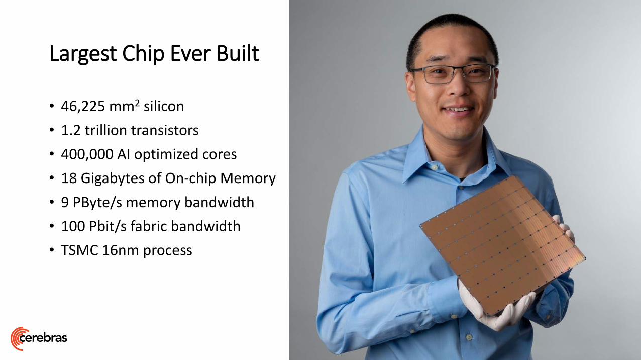
Largest Chip Ever Built
• 46,225 mm2 silicon
• 1.2 trillion transistors
• 400,000 AI optimized cores
• 18 Gigabytes of On-chip Memory
• 9 PByte/s memory bandwidth
• 100 Pbit/s fabric bandwidth
• TSMC 16nm process

Cerebras Wafer Scale Engine
Deep Learning: The Most Important Computational
Workload of Our Time
• Proliferating across industries and applications
• Large and growing portion of workload in datacenter
• Between 2012 and 2018 this workload grew 300,000x

Deep Learning Training is Hard
Size:
• Billions-trillions of ops per sample
• Millions-billions of samples per training
• Peta-exa scale compute
Shape:
• Fine-grained: A lot of parallelism; presents opportunity to accelerate
• Coarse-grained: Inherently serial

Legacy Technologies: Brute Force Parallelism
Fine-grained
• Dense vector processors (e.g. GPUs)
• Limited when compute not large uniform blocks
Coarse-grained
• Scale out clustering (e.g. PCIe, Ethernet, IB, NVLink)
• Run multiple instances of the same model (data parallel)
• Limited by inherent serial nature of problem
Result: scaling is limited and costly
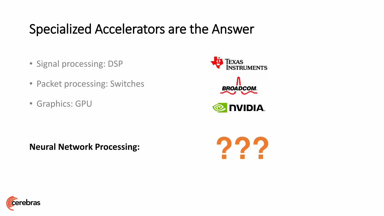
Specialized Accelerators are the Answer
• Signal processing: DSP
• Packet processing: Switches
• Graphics: GPU
Neural Network Processing: ???
The Cerebras Architecture is Optimized for DL Compute
• Core optimized for neural network primitives
• Flexible, programmable core: NN architectures are evolving
• Designed for sparse compute: workloads contain fine-grained sparsity
• Local memory: weights & activations are local with low data reuse
• Fast interconnect: layer-to-layer with high bandwidth and low latency

Flexible Cores Optimized for Tensor Operations
Key to supporting rapidly evolving NN architectures
• Fully programmable compute core
• Full array of general instructions with ML extensions
• Flexible general ops for control processing
• e.g. arithmetic, logical, load/store, branch
• Optimized tensor ops for data processing
• Tensors as first class operands
• e.g. fmac [z] = [z], [w], a
3D 3D 2D scalar

Sparse Compute Engine for Neural Networks
NN operations like nonlinearities naturally create fine-grained sparsity
• Native, sparse processing enables higher efficiency and performance
• Dataflow scheduling in hardware
• Triggered by data
• Filters out sparse zero data
• Skips unnecessary processing
• Fine-grained execution datapaths
• Small cores with independent instructions
• Maximizes utilization
• Efficiently processes dynamic, non-uniform work
Dense Network
Sparse Network
ReLU
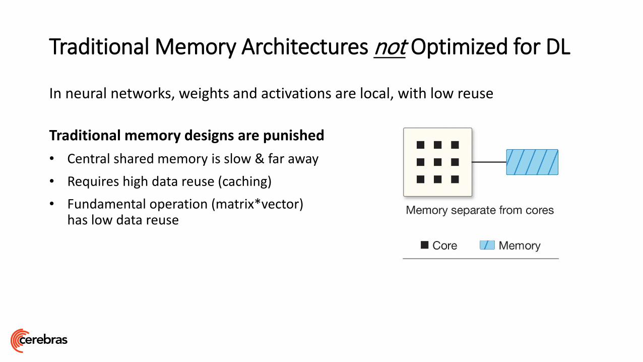
Traditional Memory Architectures not Optimized for DL
In neural networks, weights and activations are local, with low reuse
Traditional memory designs are punished
• Central shared memory is slow & far away
• Requires high data reuse (caching)
• Fundamental operation (matrix*vector) has low data reuse
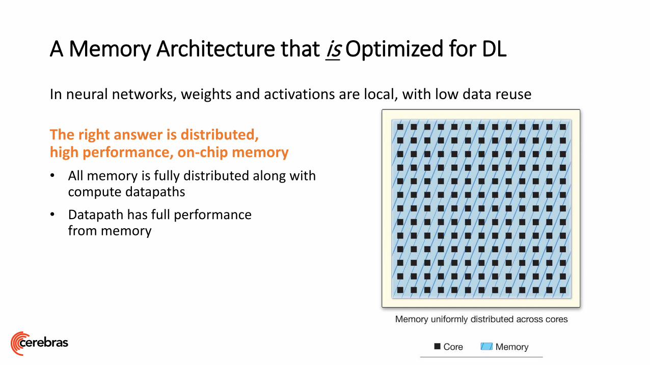
A Memory Architecture that is Optimized for DL
In neural networks, weights and activations are local, with low data reuse
The right answer is distributed, high performance, on-chip memory
• All memory is fully distributed along with compute datapaths
• Datapath has full performance from memory

High-Bandwidth Low-Latency Interconnect
Low latency intra/inter-layer local connectivity with high bandwidth
• Fast and fully configurable fabric
• Small single-word messages
• All HW-based communication avoids SW overhead
• 2D mesh topology effective for local communication
• High bandwidth and low latency for local communication
• Higher utilization and efficiency than global topologies

Achieving Radical Performance Gains
Training neural networks requires more compute than can fit on a single die
• More AI optimized cores
• More high speed on chip memory
• More fabric bandwidth at low latency connecting cores together


Build Big Chips
Big Chips Process Data More Quickly-> Producing Answers In Less Time
• Cluster scale performance on a single chip
• GB of fast memory 1 clock cycle from core
• On-chip interconnect orders of magnitude faster than off-chip
• Model-parallel, linear performance scaling
• Training at scale, with any batch size, at full utilization
• Vastly lower power & less space

Programming the Wafer Scale Engine
• Neural network models expressed in common ML frameworks
• Cerebras interface to framework extracts the neural network
• Performs placement and routing to map neural network layers to fabric
• The entire wafer operates on the single neural network
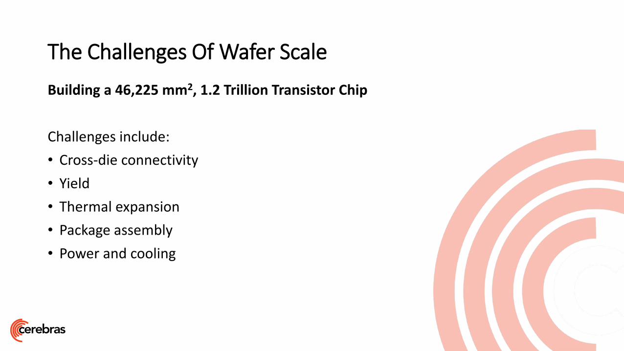
The Challenges Of Wafer Scale
Building a 46,225 mm2, 1.2 Trillion Transistor Chip
Challenges include:
• Cross-die connectivity
• Yield
• Thermal expansion
• Package assembly
• Power and cooling

Challenge 1: Cross Die Connectivity
• Standard fabrication process requires die to be independent
• Scribe line separates each die
• Scribe line used as mechanical barrier for die cutting and for test structures

Cross-Die Wires
• Add wires across scribe line in partnership with TSMC
• Extend 2D mesh across die
• Same connectivity between cores and across scribe lines create a homogenous array
• Short wires enable ultra high bandwidth with low latency

Challenge 2: Yield
Impossible to yield full wafer with zero defects
• Silicon and process defects are inevitable even in mature process
Defects
Die

Redundancy is Your Friend
• Uniform small core architecture enables redundancy to address yield at very low cost
• Design includes redundant cores and redundant fabric links
• Redundant cores replace defective cores
• Extra links reconnect fabric to restore logical 2D mesh
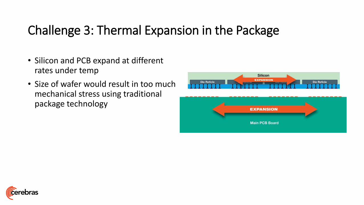
Challenge 3: Thermal Expansion in the Package
• Silicon and PCB expand at different rates under temp
• Size of wafer would result in too much mechanical stress using traditional package technology

Connecting Wafer to PCB
• Developed custom connector to connect wafer to PCB
• Connector absorbs the variation while maintaining connectivity

Challenge 4: Package Assembly
• No traditional package exists
• Package includes:
• PCB
• Connector
• Wafer
• Cold plate
• All components require precise alignment

Custom Packaging Tools
• Developed custom machines and process
• Tools to ensure precision alignment
• Tools for special handling

Challenge 5: Power and Cooling
Concentrated high density exceeds traditional power & cooling capabilities
• Power delivery
• Current density too high for power plane distribution in PCB
• Heat removal
• Heat density too high for direct air cooling

Using the 3rd Dimension
• Power delivery
• Current flow distributed in 3rd dimension perpendicular to wafer
• Heat removal
• Water carries heat from wafer through cold plate

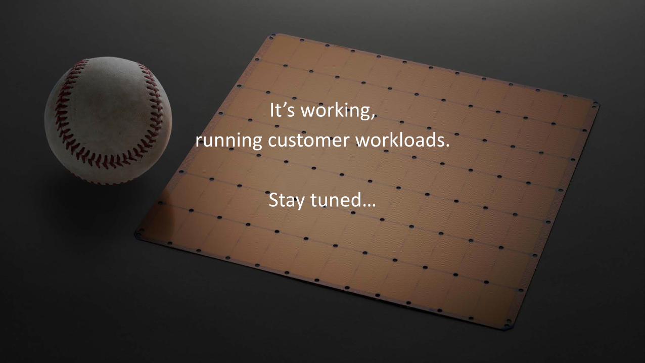
It’s working,
running customer workloads.
Stay tuned…