Wafer-to-Wafer Alignment for Three-Dimensional Integration ...

Introduction:Introduction:Wafer Level 3D IntegrationWafer Level 3D Integration
presented by
Dr. Philip GarrouMicroelectronic Consultants of NC
Research Triangle Park NC
SEMATECHSEMATECHThermal & Design Issues in 3D ICsThermal & Design Issues in 3D ICs
Albany NYAlbany NYOct 11Oct 11--12 200712 2007

OutlineOutline
DefinitionsDefinitionsDriversDrivers3D processing steps3D processing stepsProcesses at Processes at UnivUniv, Institutes, Commercial, Institutes, CommercialCurrent ApplicationsCurrent ApplicationsTechnical Barriers & IssuesTechnical Barriers & Issues
Microelectronic Consultants of NC

3D Integration vs 3D Packaging
3D IC Integration3D IC IntegrationU. Alberta
• stacked chips WB in package
• package on package stacking (PoP)
3D Packaging
Through Silicon (wafer) Vias (TSV)Wafer ThinningWafer (die) Bonding
Microelectronic Consultants of NC

3D TSV Processes3D TSV Processes
TSV from foundryTSV from foundryBefore FEOL (Before FEOL (pSipSi))Before BEOL ( W or Cu)Before BEOL ( W or Cu)
TSV after IC TSV after IC fabricatonfabricaton (after BEOL) (after BEOL)
Microelectronic Consultants of NC

Definitions Definitions
““Handle” , “Carrier”, or “Support” wafers :Handle” , “Carrier”, or “Support” wafers :Used to support the substrate during the thinning processUsed to support the substrate during the thinning processUsed to transfer layers to the 3D stackUsed to transfer layers to the 3D stack
Thinning is done: Thinning is done: After attachment to the handle wafer (before bonding)After attachment to the handle wafer (before bonding)After faceAfter face--toto--face bonding to the 3D stack (no handle)face bonding to the 3D stack (no handle)
TSV are formed either:TSV are formed either:ViasVias First First -- Before attachment to the stack Before attachment to the stack ViasVias Last Last -- After attachment to the 3D stackAfter attachment to the 3D stack
Microelectronic Consultants of NC

Interconnect SolutionsInterconnect Solutions
IMEC
2D SiP solution
• Long interchipconnections between logic & memory
SOC solution
• Large die
• design, time to market, process issues
TSV stacked Si solution
• Shortest interconnect between functions
• electricals better than SoC
Microelectronic Consultants of NC

Repartitioning DieRepartitioning Die
reduced chip area = better yieldsreduced chip area = better yieldsshorter global interconnect lines = better performanceshorter global interconnect lines = better performance
Microelectronic Consultants of NC

3D Drivers3D Drivers
• latency / bandwidth• multicore processorsLow-K integration failure
• Form Factor• Memory for portables
• Heterogeneous integration
Microelectronic Consultants of NC

Inability to smoothly integrate lowInability to smoothly integrate low--K ( K < 2.8) has hastened K ( K < 2.8) has hastened the search for solutions beyond the perceived limits of 2Dthe search for solutions beyond the perceived limits of 2D
Microelectronic Consultants of NC

MooresMoores Law Law –– Red Brick WallRed Brick Wall
SIA SIA –– Sept 2007Sept 2007““...the reality is that our ability to shrink the size of the tra...the reality is that our ability to shrink the size of the transistor nsistor will be limited by physics sometime within the next 10 to 15 yeawill be limited by physics sometime within the next 10 to 15 yearsrs””
The industry is working on the transition from the transistor tThe industry is working on the transition from the transistor to o entirely new device structuresentirely new device structures””......”” not ready for >10 not ready for >10 –– 15 years15 years””
carbon carbon nanotubesnanotubesspintronicsspintronicsmolecular switchesmolecular switches
in the interim we will see in the interim we will see ““....both evolutionary and revolutionary ....both evolutionary and revolutionary changes .... new assembly methods that will enable continuation changes .... new assembly methods that will enable continuation of of progress for decades to comeprogress for decades to come””
Specifically called out Specifically called out 3D IC integration3D IC integration
Microelectronic Consultants of NC

Intel Multicore Processors
wider busses to deliver 10-30 Gb/sec memory bandwidth
multicore systems will require 100 Gb/sec memory bandwidth
only known solution is 3D integration
face to face bonding face to face bonding Cu fusion bonding Cu fusion bonding
10 10 µµm pad pitchm pad pitch
300 mm multiprocessors using TSV
Microelectronic Consultants of NC

Intel Core 2 Processor
Ref: Puttaswammy, Loh - Ga Tech
vs
Microelectronic Consultants of NC

Form Factor for Portables
Samsung 16 Gbit stack from eight 50㎛, 2Gb NAND flash die• 0.56 mm in height • laser TSV • 30 percent thinner• 15-percent smaller footprint than equivalent WB soln
Sept 18th 2007 – ASE announces ..we wll see TSV stacked memory in mobile phoneSiPs in 2008 – 2011 (as 45 nm becomes mainstream)
Microelectronic Consultants of NC

Form Factor for DRAMForm Factor for DRAM
ELPIDA 2007Microelectronic Consultants of NC
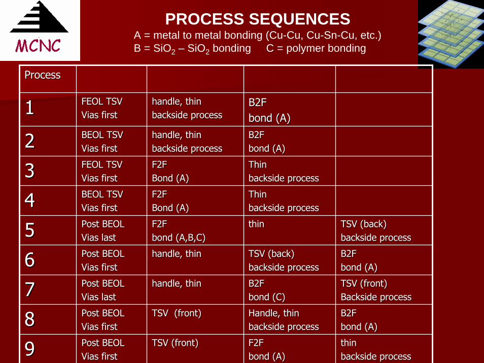
PROCESS SEQUENCESA = metal to metal bonding (Cu-Cu, Cu-Sn-Cu, etc.) B = SiO2 – SiO2 bonding C = polymer bonding
ProcessProcess
11 FEOL TSVFEOL TSVViasVias firstfirst
handle, thinhandle, thinbackside processbackside process
B2FB2Fbond (A)bond (A)
22 BEOL TSVBEOL TSVViasVias firstfirst
handle, thinhandle, thinbackside processbackside process
B2FB2Fbond (A)bond (A)
33 FEOL TSVFEOL TSVViasVias firstfirst
F2F F2F Bond (A)Bond (A)
ThinThinbackside processbackside process
44 BEOL TSVBEOL TSVViasVias firstfirst
F2F F2F Bond (A)Bond (A)
ThinThinbackside processbackside process
55 Post BEOLPost BEOLViasVias lastlast
F2FF2Fbond (A,B,C) bond (A,B,C)
thinthin TSV (back)TSV (back)backside processbackside process
66 Post BEOLPost BEOLViasVias firstfirst
handle, thinhandle, thin TSV (back)TSV (back)backside processbackside process
B2F B2F bond (A)bond (A)
77 Post BEOLPost BEOLViasVias lastlast
handle, thinhandle, thin B2F B2F bond (C)bond (C)
TSV (front)TSV (front)Backside processBackside process
88 Post BEOLPost BEOLViasVias firstfirst
TSV (front)TSV (front) Handle, thinHandle, thinbackside processbackside process
B2FB2Fbond (A)bond (A)
99 Post BEOLPost BEOLViasVias firstfirst
TSV (front)TSV (front) F2FF2Fbond (A)bond (A)
thinthinbackside processbackside process

FEOL and BEOL TSV Formation
BEOL wiring FEOL
pSi TSV FEOL devices
Via first, before FEOL
FEOL
W or Cu TSV
Via first, before BEOL
Microelectronic Consultants of NC
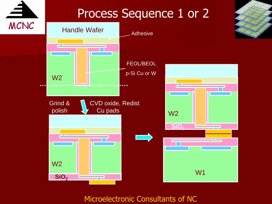
Process Sequence 1 or 2
CVD oxide, RedistCu pads
SiO2
Grind & polish
W2W1
SiO2
W2
Adhesive
FEOL/BEOL
p-Si Cu or W
Handle Wafer
W2
Microelectronic Consultants of NC

Process Sequence 3 or 4
Underfill
Grind & polish
Cu/Cu or Cu/Snbond
Wiring layers
p-Si, Cu or W
W1 W1
W2W2
Microelectronic Consultants of NC

Institutes, ConsortiaASET (1999 – 2004)* JapanFraunhofer Munich Germany IMEC BelgiumCEA-LETI FRITRI TaiwanLincoln Labs USARTI Int USA
Commercial Activity:Image Sensors:Micron USAToshiba JapanSanyo JapanFujikura JapanZiptronix USAZyCube JapanMemory:Samsung KoreaElpidia JapanTezzaron USAMicron USAProcessors:IBM USA Intel USAFoundries:TSMC Taiwan Chartered SingaporeSTATSChipPAC SingaporePkg & Assembly:ASEAmkor
*ASET 2 is being defined
Microelectronic Consultants of NC
GGLLOOBBAALL
3D3D

ApplicationsApplications
CEA Leti
Microelectronic Consultants of NC

Technical Barriers / IssuesTechnical Barriers / Issues
▪▪ Design Design ▪▪ Thermal ▪▪ TestTest
S Sapatnekar U Minnesota• thermally aware routing • thermal vias• non liquid cooling options
• size of dead zone• impact on circuits• leakage current• breakdown voltage
stacking of completed stacking of completed chips i.e. logic + memory chips i.e. logic + memory -- KGD issuesKGD issues
stacking of partitioned stacking of partitioned chips i.e. logic + logic chips i.e. logic + logic -- > KGD issues> KGD issues
How do you test partial How do you test partial circuits ??circuits ??KGD Napa KGD Napa -- addressingaddressing
Microelectronic Consultants of NC

Design Activity
• Current design tools can not be easily extended to 3D ICs • Currently - 3D integration limited to applications with regular structures i.e. memory, imagers, and FPGA’sUniversities UCLA – MEVA-3D U. Minn – “thermally conscious 3D design”U. Washington – CASCADE –UC Berkeley – 3D Magic Design software housesCadence, Mentor Graphics, R3Logic all working to develop tools for 3D design solutions
RTI 3D Conference Oct 22nd (San Francisco) 3D workshop with 2 hrs of design guidelines by Bob Patti (Tezzaron) and Lisa McIlrath (R3Logic)
Microelectronic Consultants of NC
InfrastructureInfrastructure
Infrastructure build for 3D integration is underwayInfrastructure build for 3D integration is underway•• Equipment vendorsEquipment vendors•• SematechSematech•• ConferencesConferences
IC & packaging players must all agree on standards IC & packaging players must all agree on standards ectect..
Early adopters currently look like Early adopters currently look like Imaging Memory Imaging Memory FPGAsFPGAs Memory + Logic Memory + Logic
Microelectronic Consultants of NC

Information has been pulled together
Handbook of 3D IC Integration : Technology and ApplicationsP. Garrou, P. Ramm, C. Bower Eds.
Wiley-VCH publication date: April 2008
Arkalgud – SematechBeyne – IMECBower – SempriusBrunschweiler - IBMBurkett – U. ArkansasBurns – Lincoln LabsCharlet CEA-LetideSamber – PhilipsElst – Fraunhofer MunichEnquist – ZiptronixFranzone – NCSUGarrou – MCNCHenry – CEA LetiKeast – Lincoln Labs
Authors
Linder - EVGJoly – CEAKlumpp – Fraunhofer MunichKroninger – InfineonLo – ITRILiu – RPIMak – IntelMatthias – EVGMorrow – IntelMotoyoshi – ZycubePatti – Tezzaron
Ramacher – InfineonRamm – Fraunhofer MunichRief – MITRitzdorf - SemitoolRoozeboom – NXPSapatnekar – U. MinnSchaper – U. ArkansasTakahashi – ToshibaTan – Nanyang UnivTuttle – MicronVitkavage – SematechWieland – Fraunhofer MunichWolf – Fraunhofer BerlinWonderle - Fraunhofer Munich
Microelectronic Consultants of NC

Thank You…………
Microelectronic Consultants of NC