Volume 6 Number 24 21 December 2014 Pages 14577–15348 ...
13
Nanoscale www.rsc.org/nanoscale ISSN 2040-3364 FEATURE ARTICLE Kasper Moth-Poulsen et al. The conquest of middle-earth: combining top-down and bottom-up nanofabrication for constructing nanoparticle based devices Volume 6 Number 24 21 December 2014 Pages 14577–15348
Transcript of Volume 6 Number 24 21 December 2014 Pages 14577–15348 ...

Nanoscalewww.rsc.org/nanoscale
ISSN 2040-3364
FEATURE ARTICLEKasper Moth-Poulsen et al.The conquest of middle-earth: combining top-down and bottom-up nanofabrication for constructing nanoparticle based devices
Volume 6 Number 24 21 December 2014 Pages 14577–15348
Nanoscale
FEATURE ARTICLE
Cite this: Nanoscale, 2014, 6, 14605
Received 3rd July 2014,Accepted 15th August 2014
DOI: 10.1039/c4nr03717k
www.rsc.org/nanoscale
The conquest of middle-earth: combiningtop-down and bottom-up nanofabrication forconstructing nanoparticle based devices†
Yuri A. Diaz Fernandez,‡§a Tina A. Gschneidtner,§a Carl Wadell,b
Louise H. Fornander,a Samuel Lara Avila,b Christoph Langhammer,b
Fredrik Westerlunda and Kasper Moth-Poulsen*a
The development of top-down nanofabrication techniques has opened many possibilities for the design
and realization of complex devices based on single molecule phenomena such as e.g. single molecule
electronic devices. These impressive achievements have been complemented by the fundamental under-
standing of self-assembly phenomena, leading to bottom-up strategies to obtain hybrid nanomaterials
that can be used as building blocks for more complex structures. In this feature article we highlight some
relevant published work as well as present new experimental results, illustrating the versatility of self-
assembly methods combined with top-down fabrication techniques for solving relevant challenges in
modern nanotechnology. We present recent developments on the use of hierarchical self-assembly
methods to bridge the gap between sub-nanometer and micrometer length scales. By the use of non-
covalent self-assembly methods, we show that we are able to control the positioning of nanoparticles on
surfaces, and to address the deterministic assembly of nano-devices with potential applications in plas-
monic sensing and single-molecule electronics experiments.
Introduction
One of the most exciting challenges in modern nanotechnologyresides in the middle size range, bridging molecular lengthscales and microsized objects.1 Considerable efforts have beendevoted to the development of top-down nanofabricationmethods,2–9 and the impressive progress achieved by miniaturi-zation technology in the last decades has led to advanced omni-present microprocessors and portable devices. Yet, top-downlithography techniques are at the present level not able to fabri-cate systems with molecular or atomic precision.5,10–14
In a parallel effort, the understanding of the physical andchemical phenomena responsible for self-organization of
molecules and materials into complex hierarchical structureshas launched a quest towards self-fabricating systems basedon supramolecular chemistry.15–20 Experimental and theore-tical contributions from different research fields have contri-buted to the development of self-assembled materials, formedby collective interactions of organic molecules, inorganicnanoparticles (NPs), and hybrid composites.21–25
If we consider the number of scientific publications relatedto top-down and bottom-up approaches in the last decades asan indicator of the development of these research fields, wecan affirm that there has been a continuous growth of interestof the scientific community in these topics, catalysed by theimprovement of electron microscopy techniques, scatteringmethods, scanning probe techniques, and other characteri-zation tools able to provide detailed information on processesand structures with atomic resolution.26
While both extreme domains, the bottom-up and the top-down fields, have been consolidated over years of fundamentaland technological research, the intermediate length-scale, the“middle” field, started to be intensively explored onlyrecently.1,27–32 One plausible reason for this delayed debutcould be the lack of experimental techniques able to addressproperties of single, or just-a-few, molecules, and the inabilityto accurately control the fate of sub-nanometric objects. Onerelevant challenge related to the fabrication of devices that
†Electronic supplementary information (ESI) available: Additional SEM of NPsub-monolayers under different conditions. TEM images of cubic Pd NPs. SeeDOI: 10.1039/c4nr03717k‡Current address: Open Innovation Hub for Antimicrobial Surfaces, SurfaceScience Research Centre, Department of Chemistry, University of Liverpool,Liverpool L69 3BX, UK.§YADF and TAG contributed equally to this work.
aDepartment of Chemical and Biological Engineering, Chalmers University of
Technology, SE-412 96 Gothenburg, Sweden.
E-mail: [email protected] of Applied Physics, Chalmers University of Technology, SE-412 96
Gothenburg, Sweden
This journal is © The Royal Society of Chemistry 2014 Nanoscale, 2014, 6, 14605–14616 | 14605
Ope
n A
cces
s A
rtic
le. P
ublis
hed
on 2
1 A
ugus
t 201
4. D
ownl
oade
d on
3/2
1/20
22 1
1:23
:33
PM.
Thi
s ar
ticle
is li
cens
ed u
nder
a C
reat
ive
Com
mon
s A
ttrib
utio
n 3.
0 U
npor
ted
Lic
ence
.
View Article OnlineView Journal | View Issue
combine single-molecule length scale objects with macro-scopic objects, is the requirement of controlled positioning ofNPs and molecules at pre-defined sites at surfaces.33 In thepresent article we highlight some efforts that our researchgroup, together with several collaborators, have been involvedin to address this issue, and we also discuss challenges andfuture perspectives in this field. Furthermore, we present somerecent results related to the combination of self-assemblymethods and top-down fabrication techniques to control posi-tioning of NPs at surfaces.
Results & discussionSolution based self-assembly methods
One major challenge in the development of single moleculedevices is the incompatibility in length scales between mole-cular dimensions and macroscopic instruments. One of theapproaches used to overcome this challenge is based on theself-assembly in solution of nanometric junctions between NPsand the placement of these proto-devices on micro-fabricatedstructures, i.e. electrodes connected to macroscopic source-drain electrodes.28,34–36 Using this approach, Bar-Joseph et al. in2005 probed, for the first time, the transport properties across asingle molecule that bridges two metal NPs.37 The interest ofthe research community has remained on this strategy forseveral years, developing sophisticated synthetic approaches tobuild NP aggregates of controlled size in solution,36,38–43 and toplace these proto-devices onto electrodes.34–38
Bjørnholm et al. developed a bottom-up approach that com-bines nanoparticle self-assembly and seed-growth methods tosynthetize end-to-end linked gold nanorods (AuNRs).44 Whileseveral procedures for the end-to-end linking of AuNRs involvemodification of the already synthetized AuNRs,45–48 Bjørnholmet al. assembled spherical NPs into small aggregates (i.e.dimers) connected by dithiol PEG linker molecules, and thenused these aggregates as seeds for the growth of AuNRs. Theresulting structures consisted of two 500 nm long AuNRs sepa-rated by a gap of 2 nm. Although the yields of this processwere not particularly high, the possibility of combining thesehighly anisotropic proto-devices with micro-electrodes pro-vides a promising path to overcome the challenges of singlemolecule transport measurements.28,49
Several methods have been proposed to control NP cluster-ing stoichiometry, based on topological constrains,50–52 on theasymmetric functionalization of NP surfaces53–59 or exploitingbio-mimetic interactions.39,60–78 These strategies allow the syn-thesis of NP clusters of well-defined composition (dimers,trimers, etc.) combining identical NPs (homoaggregates)43,79–81
or NPs of the same material, but with different sizes (hetero-aggregates).82,83 A few examples have been presented for thecombination of NPs of different materials within the samenanocluster.84–86 This kind of nanostructures could providenew insights on the electronic properties of molecules at asym-metric metal junctions and introduce an additional drivingforce for controlled transport- and conductance-switching,
considering the differences in Fermi energy between twodifferent materials.87–90
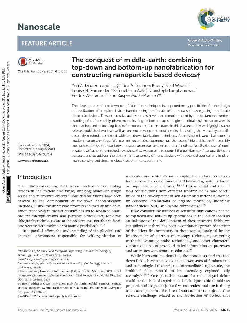
Recently a general self-assembly strategy to synthesize NPheterodimers of two different materials was introduced byMoth-Poulsen et al.86 The method is based on the delicatebalance between repulsive and attractive interactions respon-sible for colloidal stability, and allows the synthesis of tailoredstructures (heterodimers) with up to 42% of relative abun-dance among the population of single particles and aggregates.These heterodimers are obtained by combining sphericalAuNPs and AgNPs with different kinds of PdNPs and AuNPshaving distinctive crystallographic properties, shapes and sizes(Fig. 1). The possibility of controlling the self-assembly of oppo-sitely charged NPs, exploiting electrostatic interactions, opensnew possibilities for the synthesis of metal nanoclusters ofdefined composition. Understanding the experimental con-ditions leading to selective self-assembly of metal NPs of oppo-site charge over bulk aggregation is a challenge that would havea considerable impact on the development of new hybridmaterials. Furthermore, these bimetallic systems might havepromising properties for plasmonic sensing of chemicalreactions,91–93 plasmon-enhanced catalysis,94–103 and thermo-electric power generation.104 Therefore the development of newsynthetic strategies to obtain defined metal-clusters will be arelevant topic of research in the future.
Template driven self-assembly of NPs at interfaces andsurfaces
One common limitation of the solution based self-assemblymethods for building NP junctions is the inability to producehigh yields of the tailored structures, requiring post-synthesispurification methods, that affect the actual yields. Addition-ally, purely solution-based single-molecule electronic devices
Fig. 1 Noble metal nanoparticle heterodimers synthetized using non-covalent electrostatic self-assembly of colloids of different shapes, sizes, andmaterials: (A) Ag (spherical90 nm) and Pd (cube25 nm); (B) Ag (spherical90 nm)and Pd (cube70 nm); (C) Au (spherical90 nm) and Pd (cube25 nm); (D) Au(spherical90 nm) and Pd (cube70 nm); (E) Au (spherical90 nm) and Au(cube35 nm); (F) Ag (spherical90 nm) and Au (cube35 nm) (reproduced byACS AuthorChoice – Open Access agreement from T. A. Gschneidtner,Y. A. D. Fernandez, S. Syrenova, F. Westerlund, C. Langhammer and K. Moth-Poulsen, Langmuir, 2014, 30(11), 3041–3050).86
Feature article Nanoscale
14606 | Nanoscale, 2014, 6, 14605–14616 This journal is © The Royal Society of Chemistry 2014
Ope
n A
cces
s A
rtic
le. P
ublis
hed
on 2
1 A
ugus
t 201
4. D
ownl
oade
d on
3/2
1/20
22 1
1:23
:33
PM.
Thi
s ar
ticle
is li
cens
ed u
nder
a C
reat
ive
Com
mon
s A
ttrib
utio
n 3.
0 U
npor
ted
Lic
ence
.View Article Online
are not feasible at the current state-of-the-art, and probably willnever be conceived. Therefore, for applications, the methodsbased on self-assembly of proto-devices in solution will dependon micro- or nanofabrication techniques at surfaces, to guideand position nanoscale objects from solution to pre-deter-mined, tailored sites. In this sense, the use of deterministicassembly of nanometric objects directly on engineered surfaceswith controlled positioning and orientation can provide inter-esting paths for the bottom-up fabrication of devices.105–107
Different experimental approaches have been proposed tocombine self-assembly solution methods with solid-state archi-tectures.44 The use of self-assembly methods at interfaces pro-vides several advantages for the design and build-up ofsystems with low dimensionality (i.e. lower than 2). The inter-face between two environments of very different propertiesprovides topological and energetic constrains that favour theemergence of supra-molecular structures with characteristicsthat might differ from the properties of bulk materials. Fur-thermore, thin films usually display high transmittance, rela-tively dynamic behaviour, and well-defined structuralproperties at different length scales. One promising strategyconsists in the direct self-assembly of components at liquid–air interfaces, followed by subsequent transferring of thesestructures onto the surface of top-down fabricated electrodes.Following this strategy, Bjørnholm et al. succeeded with thefabrication of pseudo one-dimensional molecular electronicnetworks, consisting of segments of AuNPs separated by1–3 nm wide gaps and interconnected by conjugated organicmolecules.108 The networks were obtained by lipid templatedself-assembly of AuNPs at the air–water interface. The Langmuirmonolayer obtained was compressed and subsequently trans-ferred horizontally (Langmuir–Schäfer) to a solid support with aprefabricated network of gold microelectrodes prepared by top-down UV/e-beam lithography. The electronic properties of thispseudo one-dimensional molecular electronic circuit werecharacterized by using macroscopic electrodes and a conductiveAFM tip as the probe. This procedure can be easily adapted toany kind of molecular system having a strong affinity for thegold surface, while the entire circuit is built by a series of purelychemical manipulations under standard lab conditions.
A similar approach was applied to the preparation ofordered structures of gold AuNPs at the nanometer lengthscale, by using amphiphilic polymers as templating agents.109
The polymers used had a bi-functionalized poly(p-phenylene)backbone, with phenolic groups on one side and alkoxy chainson the other side, giving the polymer amphiphilic properties.These polymers are able to form stable mono- and multi-layered Langmuir–(Blodgett/Schäfer) films by horizontal andvertical lifting.110–112 Furthermore, these polymeric moleculeshave interesting photophysical properties in solution and assolid films, making them good candidates as a template forself-organized nanostructures.112–114 The ability to control themorphology of the gold pattern by applying different surfacepressures on the composite Langmuir film is a promisingstrategy for large-area self-assembly of architectures, useful todesign complex molecular electronic devices.
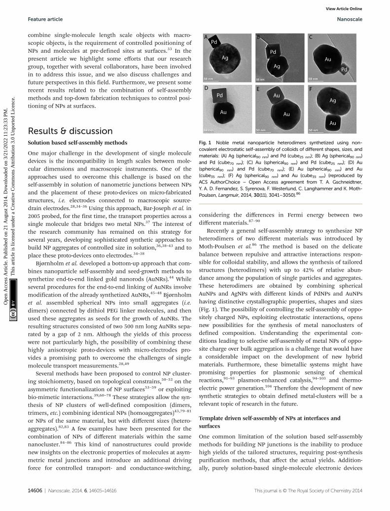
The template structures used for the self-assembly of NPscan be directly built on solid surfaces, using top-down nano-fabrication procedures. An interesting example of this strategyhas been presented by Bjørnholm et al. demonstrating in situgrowth of AuNRs with positional control and alignment inwell-defined poly(methyl methacrylate) nanochannels.115
Spherical AuNPs were self-assembled at specific sites of thepatterned substrates and the AuNRs were grown in situ using aseed-mediated synthetic approach (Fig. 2). The system allowedfor fabrication of multiple nanogap junctions on a single chipwith AuNRs acting as nanoelectrodes. The implementation ofthis method on surfaces pre-patterned with metallic electrodesis a promising strategy towards the development of parallelfabrication of single-molecule electronic devices. These resultsdemonstrate the strength of combining top-down templatingand bottom-up growth of electrically addressable devices. Thetop-down preparation of the metallic contacts prior tonanogap formation eliminates potential damage of thenanogap due to post-processing steps. The incorporation ofπ-conjugated systems prior to seeding leads to better control ofthe molecular orientation in the gaps, however some chal-lenges remain in terms of yields of the devices.
An alternative, and very promising, strategy consists of thedirect self-assembly of NPs within templates fabricated on sur-faces. Extensive work carried out by Alivisatos et al., Wolf et al.,and Vaia et al. has demonstrated the versatility of using capil-larity forces combined with lithografically defined templates todrive the self-organization of NPs on nanoengineeredsurfaces.106,107,116–123 The incorporation of DNA-directed self-assembly methods on patterned surfaces has allowed furthercontrol of the morphology and orientation of the assembled
Fig. 2 Schematic representation of stepwise assembly of nanoparticles(A and B) followed by in situ growth of nanorods (C) and removal of thedirecting PDMS template (D). (E–H) show SEM micrographs of success-fully grown gold nanorods. Reprinted with permission from T. Jain,S. Lara-Avila, Y.-V. Kervennic, K. Moth-Poulsen, K. Nørgaard, S. Kubatkin,and T. Bjørnholm, ACS Nano, 2012, 6, 3861–3867. Copyright 2012 Amer-ican Chemical Society.)
Nanoscale Feature article
This journal is © The Royal Society of Chemistry 2014 Nanoscale, 2014, 6, 14605–14616 | 14607
Ope
n A
cces
s A
rtic
le. P
ublis
hed
on 2
1 A
ugus
t 201
4. D
ownl
oade
d on
3/2
1/20
22 1
1:23
:33
PM.
Thi
s ar
ticle
is li
cens
ed u
nder
a C
reat
ive
Com
mon
s A
ttrib
utio
n 3.
0 U
npor
ted
Lic
ence
.View Article Online

structures,124,125 while the use of electrostatic trappinginduced by surface topology has also been demonstrated.126
Recently, a top-down nanofabricated template has beencombined with directed capillary assembly to place AuNRs in ahighly deterministic pattern, forming continuous chains withdimensionality equal to unity.106 Within these straight chains,the AuNRs were aligned in one chosen direction with an end-to-end configuration. The precise control of the process leadsto the formation of gaps of ∼6 nm between the individual con-stituents of the chain. The conditions for optimum quality andyield of AuNR chain assembly have been investigated, explor-ing the influence of template size and assembly tempera-ture.106 This approach also allows the transfer of the self-assembled AuNR chains from the assembly template onto aSi/SiO2 target substrate, thus establishing a platform for avariety of nanoscale electronic and optical applications. Aproof-of-principle experiment has been shown in thesesystems, performing electrical measurements on contactedAuNR chains before and after their immersion in a solution ofthiol-end capped oligophenylenevinylene molecules. Theincrease in the conductance by three orders of magnitude inthe presence of the conjugated oligomer indicates molecular-mediated charge transport across the nanogaps.106
Capillarity-assisted particle-assembly methods have becomesophisticated, allowing the design and implementation ofcomplex nanostructures with extremely high precision. One ofthe most impressive examples, presented by Wolf et al., has intro-duced the concept of cascade assembly to build-up complex pat-terns combining different kinds of nanoparticles.127
Capillary forces have also been used by Mirkin et al. toachieve shape selectivity during the self-assembly process,128
and to place segmented nanowires in well-defined bidimen-sional arrays.129
Despite the growing understanding of fundamental prin-ciples of capillary forces in confined nanostructures, themethods proposed for capilarity-driven self-assembly of NPs areoften specific for the systems studied. Combining nanofabri-cated surfaces with capilary forces requires delicate tuning ofseveral experimental variables, and allows precise control of thepositioning of NPs after considerable experimental effort. Inthis sense the development of new general strategies to placeNPs in pre-defined positions at surfaces, avoiding topologicalconstrains, would be a breakthrough in this research field.
NP positioning by electrostatic soft-template directedself-assembly
A relevant challenge when assembling nanopartilces on solidsurfaces is the selectivity and the control of the NP adhesionin specific patterns and at preferred locations on the surface,especially to be able to control adhesion and thereby the siteswhere nanoscale objects are positioned. Microspheres havebeen successfully self-assembled on patterned structures, andthe factors controlling the self-organization of these objectshave been studied.130,131 Several methods for controlled posi-tioning of NPs on surfaces have also been investigated.132,133
One interesting approach is based on the electrophoretic depo-
sition of NPs on pre-patterned surfaces.134–136 This methodallows faster processing times with respect to other depositiontechniques.137 Capilary forces, discussed in the previoussection, have been combined with top-down nanofabricatedtemplates to control orientation and positiong of NPs onsurfaces.106,107,116–129 Selective chemical functionalization ofsurfaces has also been used to drive the self-assembly of NPsexploiting the chemistry of silane-derivatives on Si surfaces138–140
and using micro-contact printing on gold surfaces.141
Direct surface self-assembly methods are versatile and allowthe development of more advanced procedures to increase thecontrol of nanostructure positioning and topographical orien-tation of small objects. At the current state-of-the-art, thehighest control over NPs orientation and positioning can beachieved by the combination of top-down engineering of sur-faces and bottom-up self-assembly methods.127,129
Efficient top-down methods for the fabrication of electrodesand complex surface patterns have become available in the lastdecades, and the considerable improvement of spatial resolu-tion and large-area reliability of these techniques has contribu-ted to the development of different research areas.142
Exploiting the distinctive chemical properties of Si- andmetal-based surfaces, it has been possible to build self-assembled sub-monolayers of NPs with well-defined structuralproperties. The possibility of exploiting non-covalent inter-actions to direct the self-assembly of NP monolayers is veryattractive, since it takes advantage of collective interactionsresponsible for the properties of supramolecular systems.
The strategy we present here is based on a silane-free versa-tile method able to address the challenge of NP selective posi-tioning based on the direct self-assembly of NPs from colloidalsolutions on nanofabricated oxidized Si surfaces, avoiding theuse of capillarity interactions and without external electrophor-etic fields. As it will be shown below, we have used self-assembled lipid bilayers as a soft template to reduce unspecificbinding of NPs to material-specific areas of the surface. Thismethod allows controlled self-assembly and selective position-ing of objects with nanometric space-resolution using ageneral strategy that we envision to easily extend to differentkinds of surface materials and NPs.
SiO2 surfaces are well known to promote non-covalentadsorption of positively charge molecules and NPs. Thiscapacity can be used to form homogeneous self-assembledsub-monolayers of metal NPs capped with cationic surfactants.Several methods for the synthesis of shaped metal NPs involvecationic amphiphilic molecules as stabilizers of specific crys-tallographic facets on the metal surface.28,143–149 The removalor exchange of these surfactant molecules from the particlesurface after the synthesis, without compromising the stabilityof the colloids, is a challenging task.28,86
We have observed a general self-assembly behaviour onSiO2 or oxidized Si substrates for several NP systems stabilizedby cationic surfactants, irrespectively of the shape, the size orthe material of the NPs (Fig. 3a,b; and ESI SI2, SI3†). The NPsused for these experiments were synthetized by methods pre-viously reported, that introduce cetyltrimethyl ammonium
Feature article Nanoscale
14608 | Nanoscale, 2014, 6, 14605–14616 This journal is © The Royal Society of Chemistry 2014
Ope
n A
cces
s A
rtic
le. P
ublis
hed
on 2
1 A
ugus
t 201
4. D
ownl
oade
d on
3/2
1/20
22 1
1:23
:33
PM.
Thi
s ar
ticle
is li
cens
ed u
nder
a C
reat
ive
Com
mon
s A
ttrib
utio
n 3.
0 U
npor
ted
Lic
ence
.View Article Online

bromide or chloride as capping agents (further details as ESISI1†).28,144–146 These synthetic routes yield NPs with low dis-persity in terms of shape and size. The introduction of the cat-ionic surfactants provides a net positive charge on the surfaceof the colloids. We have successfully formed self-assembledsub-monolayers of Pd nanocubes, Au nanocubes, and Aurhombic dodecahedra NPs of different sizes, on oxidized Sisurfaces, demonstrating the versatility of this approach (SEMimages of representative examples of NP sub-monolayers arepresented in Fig. 3 and in ESI†).
The process used for the preparation of the NP sub-mono-layers is based on drop-casting on clean oxidized Si surfaces,followed by incubation in solutions for 30 minutes, andrinsing with deionized water. The surface of the Si wafer wascleaned with oxygen plasma before use, but also other kindsof oxidative cleaning procedures, such as piranha etching orthermal annealing, are effective for this deposition technique.The procedure leads to homogeneous sub-monolayers of NPsevenly distributed on the surface of oxidized Si wafers. TheseNP sub-monolayers were stable after rinsing with water as wellas with organic solvents (see SI4† for further details).
On the other hand, the surface properties of oxidized Sisubstrates can be modified to control the adhesion on the par-ticles to the surface. We have previously shown that surfacepassivation by coating with lipid bilayers almost completelyeliminates the non-specific adhesion of biomolecules and NPswithin SiO2 nanochannels.151 The lipid-surface passivationmethod has been demonstrated to perform better than stan-dard passivation protocols, i.e. bovine serum albumin (BSA)coating. This approach has also the advantage of self-healing,which is a typical characteristic of supramolecular systems thatallows the self-assembled structure to correct intrinsic orinduced defects by exchange of molecules with the solutionand rearrangement on the surface. Freely moving quantumdots, proteins and protein–DNA complexes have been success-fully studied in devices passivated with lipids, preventing inter-ference of non-specific chemisorption.150,151
The presence of self-assembled lipid bilayers on the surfaceof SiO2 drastically prevents the adsorption of the NPs investi-gated in this work. The surface density of NPs is decreasedby more than two orders of magnitude in the presence ofthe bilayers (Fig. 3c), with respect to the clean SiO2
surface (Fig. 3b). This non-covalent passivation strategy isrelatively simple, did not compromise the surface propertiesof the substrate on a permanent basis, and results in a promis-ing strategy for the self-assembly of nanoscale deviceson surfaces.
When using lipid bilayers on flat surfaces, there are twomajor experimental challenges to overcome: the lateraldiffusion of the bilayers on open surfaces and the requirementof a continuously wet environment. We spread lipid bilayerliposomes, 100 nm in diameter, on the oxidized Si surface tospontaneously form self-assembled bilayers. These structuresrequire a mechanical barrier to contain the lateral diffusion ofthe lipids on the flat surface, and for this reason, before thewet functionalization, we fabricated a PMMA pool on the edgeof the oxidized Si surface, that provides mechanical stability tothe lipid bilayer, and also acts as container for the droplet ofsolution on top of the clean oxidized Si surface. Within thispool, the solutions are exchanged using source and drain pip-ettes simultaneously, in order to avoid the bilayer-functiona-lized surface to get dry. Following this procedure it is possibleto substitute the previous solution with a new one, allowingthe change of buffer solutions, rinsing the surface, and remov-ing the colloidal solutions, without affecting the stability ofthe lipid bilayers on the oxidized Si surface.
Fig. 3 Self-assembled NP sub-monolayer on oxidized Si surfaces: (a, b)PdNPs (25 nm) on clean oxidized Si surfaces at different magnifications;(c) Lipid bilayer passivation preventing PdNP sub-monolayer formationon Si surface.
Nanoscale Feature article
This journal is © The Royal Society of Chemistry 2014 Nanoscale, 2014, 6, 14605–14616 | 14609
Ope
n A
cces
s A
rtic
le. P
ublis
hed
on 2
1 A
ugus
t 201
4. D
ownl
oade
d on
3/2
1/20
22 1
1:23
:33
PM.
Thi
s ar
ticle
is li
cens
ed u
nder
a C
reat
ive
Com
mon
s A
ttrib
utio
n 3.
0 U
npor
ted
Lic
ence
.View Article Online
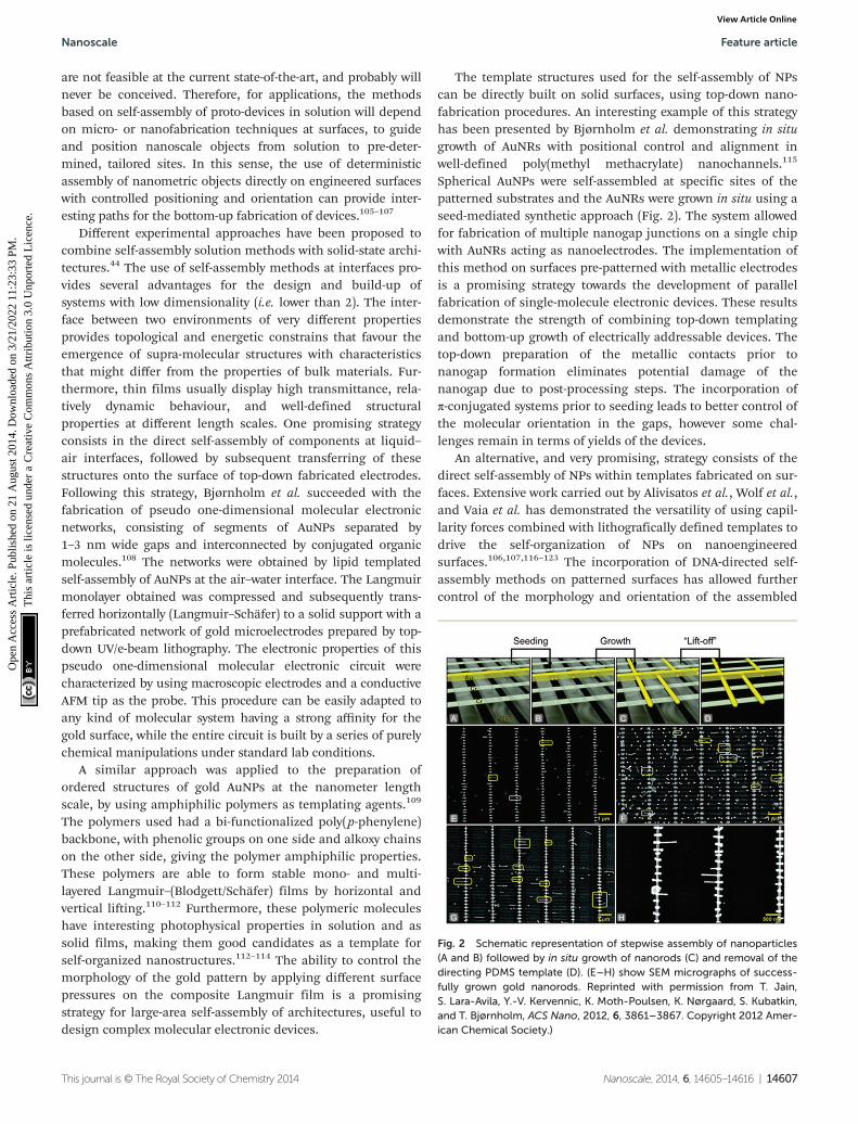
The solutions were exchanged gradually, and equilibrationwas allowed between one functionalization and the next. Thesubstrates were initially rinsed with the same buffer solutionused to store the liposomes, and when the liposomes wereintroduced on the surface, 15 minutes of stabilization timewas allowed. The lipid solution was rinsed first with liposomebuffer and thereafter with water, before introducing the col-loidal solutions. When needed, several rinsing steps were per-formed in order to completely remove the residues from theprevious solution. After rinsing the NP solution, the surfacecan be dried, plasma cleaned, and analysed using SEM(Fig. 3). The full description of the preparation of NP sub-monolayers is provided as ESI (ESI1 and Fig. S1†).
The adhesion of charged NPs to the surface can also be tai-lored by adjusting the surface potential of metal surfaces.152
We have used chemisorption of charged molecules on Au sur-faces to change the surface charge. Gold has particular affinityfor thiols, and the properties of self-assembled molecularmonolayers of thiols on noble metal surfaces have been exten-sively studied.153–158 We could not observe the formation ofself-assembled sub monolayers of metal NPs stabilized by cat-ionic surfactants on clean gold surfaces (Fig. 4a), while goldsurfaces functionalized with sulfonate groups promote theadhesion of positively charged NPs (Fig. 4b). These distinctiveproperties can be exploited for non-covalent self-assembly ofmore complex NP architectures and devices, and to interfacebottom-up self-assembled proto-devices with top-down fabri-cated nano- and micro-structures.27
Direct self-assembly methods can be used to control theplacement of NPs on nano-engineered surfaces, and to modifythe morphology of NP monolayers. Similarly, lipid bilayers can
Fig. 4 Self-assembled sub-monolayer of PdNPs (25 nm): (a) on plasma-cleaned gold surface; (b) on gold surface functionalized with MESNa.
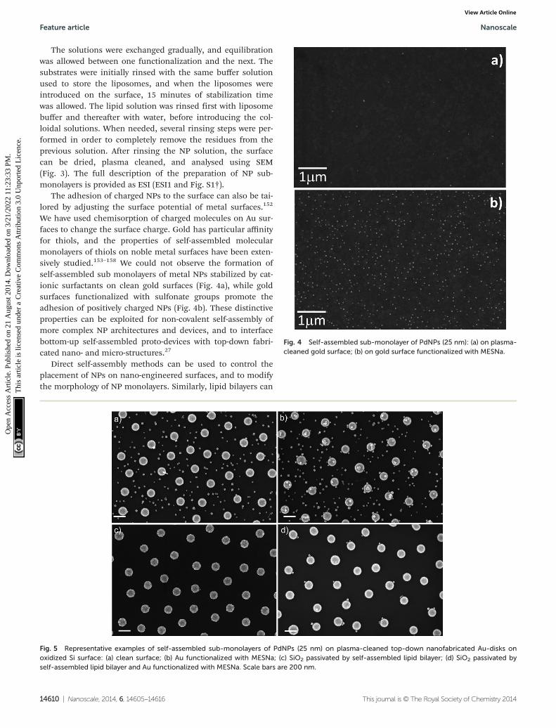
Fig. 5 Representative examples of self-assembled sub-monolayers of PdNPs (25 nm) on plasma-cleaned top-down nanofabricated Au-disks onoxidized Si surface: (a) clean surface; (b) Au functionalized with MESNa; (c) SiO2 passivated by self-assembled lipid bilayer; (d) SiO2 passivated byself-assembled lipid bilayer and Au functionalized with MESNa. Scale bars are 200 nm.
Feature article Nanoscale
14610 | Nanoscale, 2014, 6, 14605–14616 This journal is © The Royal Society of Chemistry 2014
Ope
n A
cces
s A
rtic
le. P
ublis
hed
on 2
1 A
ugus
t 201
4. D
ownl
oade
d on
3/2
1/20
22 1
1:23
:33
PM.
Thi
s ar
ticle
is li
cens
ed u
nder
a C
reat
ive
Com
mon
s A
ttrib
utio
n 3.
0 U
npor
ted
Lic
ence
.View Article Online

drive the formation of self-assembled monolayers on selectedareas of nanofabricated surfaces. Combining these two comp-lementary features, we have been able to build up prototypesof self-assembled plasmonic sensors based on nanofabricatedgold disks linked to palladium NPs (Fig. 5d). The gold diskswere nanofabricated on SiO2 surfaces using Hole-Mask Col-loidal Lithography.159 A 5 nm thick Cr layer was used toimprove the adhesion of the Au-structures to the oxidized Si-surface. As discussed above, CTAB stabilized PdNPs are able toform sub-monolayers on the surface of the SiO2, and thereforethey are spread evenly on the nanofabricated plasmonic sur-faces (Fig. 5a), and only 15% of the Au structures are incontact with PdNPs. When the Au-surface is functionalizedwith the negatively charged thiol–sulfonate molecules (sodium2-mercaptoethanesulfonate, MESNa), the self-assembly of posi-tively charged PdNPs is preferentially driven towards the Au
surface, allowing more than 99% of the Au-disks to hostPdNPs, but still non-specific adsorption is observed on the oxi-dized Si surface (Fig. 5b). The combination of lipid-passivationwith functionalization of Au with MESNa leads to the exclusivepositioning of PdNPs on 56% of the Au structures, effectivelypreventing adhesion to oxidized Si-surfaces (Fig. 5d). Whenthe lipid passivation was used without MESNa on Au (Fig. 5c),less than 5% of the Au-structures were occupied by PdNPs,therefore the combination of MESNa-functionalization on goldand lipid-bilayer passivation on oxidized Si is essential fordriving the self-assembly towards the Au-structures.
This step-wise functionalization approach allows us toselectively modify the surface properties of oxidized Si and Au,exploiting the specific interactions of surface active species ondifferent materials. The strategy developed, similar to theapproach used on oxidized Si wafers, also requires the continuous
Fig. 6 Schematic representation of the layer-by-layer strategy used for the functionalization of top-down nanofabricated structures: (a) startingsurface, (b–c) MESNa functionalization of Au surface; (d–e) SiO2 passivation with lipid bilayers; (f–g) colloidal deposition; (h) final surface.
Nanoscale Feature article
This journal is © The Royal Society of Chemistry 2014 Nanoscale, 2014, 6, 14605–14616 | 14611
Ope
n A
cces
s A
rtic
le. P
ublis
hed
on 2
1 A
ugus
t 201
4. D
ownl
oade
d on
3/2
1/20
22 1
1:23
:33
PM.
Thi
s ar
ticle
is li
cens
ed u
nder
a C
reat
ive
Com
mon
s A
ttrib
utio
n 3.
0 U
npor
ted
Lic
ence
.View Article Online

and smooth exchange of solutions on top of the nanofabri-cated structures, in order to avoid drying and preserve thestructural integrity of the lipid bilayers (Fig. 6). In this case, wehave also used the PMMA pool on the edge of the wafer. Thetop-down nanofabricated Au structures were functionalizedwith MESNa (Fig. 6b), keeping the surface in contact with thesolution (6 × 10⁻⁵ M of MESNa in water) for 2 hours beforerinsing with water (Fig. 6c). The subsequent steps (Fig. 6c–h)were performed following the procedure described above forflat oxidized Si substrates. The self-assembled structures arestable upon drying and plasma cleaning, allowing SEM charac-terization (Fig. 5).
To further demonstrate the control of the positioning ofPdNPs on oxidized Si surfaces, we explored other geometricalshapes of gold patches. Specifically, we used oxidized Si wafersonto which gold lines were patterned using e-beam lithogra-phy (Fig. 7). The selectivity of NP self-assembly was againachieved by lipid-bilayer passivation of the SiO2 surface, andfunctionalization of the Au-structures with MESNa, followingthe strategy depicted in Fig. 6. This electrostatic soft-templatedirected self-assembly method allows highly selective self-
assembly of PdNPs on the Au-surface, producing a surfacedensity of PdNPs on gold that is 4000 times greater comparedto that on the SiO2 surface.
Probably the most relevant strength of the non-covalentself-assembly methods presented here is illustrated in the lowmagnification SEM images in Fig. 7b and 7e, showing scalabil-ity from small to large area devices. This capacity combinedwith the versatility of deterministic assembly proceduresallows simultaneous fabrication of several independentdevices on macroscopic surfaces.
Concluding remarks
The impressive development of supra-molecular chemistry andself-assembly methods in the last decades has contributed tothe establishment of a well-structured experimental and concep-tual framework that provides promising routes for the design ofadvanced functional structures such as single molecule elec-tronic devices, nano-actuators and nano-machines. Manyexamples of functional nano-devices are assembled, fabricated,
Fig. 7 PdNPs self-assembled on gold top-down fabricated structures: (a) clean Au lines patterns on clean oxidized Si wafer, (b–f ) MESNa functiona-lized Au-lines pattern on oxidized Si lipid-bilayer passivated wafer (different magnifications, and different patterns).
Feature article Nanoscale
14612 | Nanoscale, 2014, 6, 14605–14616 This journal is © The Royal Society of Chemistry 2014
Ope
n A
cces
s A
rtic
le. P
ublis
hed
on 2
1 A
ugus
t 201
4. D
ownl
oade
d on
3/2
1/20
22 1
1:23
:33
PM.
Thi
s ar
ticle
is li
cens
ed u
nder
a C
reat
ive
Com
mon
s A
ttrib
utio
n 3.
0 U
npor
ted
Lic
ence
.View Article Online
or deposited on macroscopic electrodes or bulk substrates. Thisdichotomy seems to be intrinsic in nature and there is noobvious shortcut to bypass it at the current state-of-the-art.
In recent years the research community has begun toexploit the combination of “bottom-up” & “top-down”approaches, finding paths to merge these two strategiesefficiently. The challenge of developing reliable methods toproduce large scale arrays of nano devices connected incircuit-like architectures is not solved yet, and one can foreseethat this will be an exciting research topic for the comingyears. The combination of soft-matter masks with metal andmetal oxide NP chemical and physical synthesis might lead tounexpected scientific breakthroughs. Such breakthroughsmight be associated with template-free self-assembly methods,able to be scaled-up to large surfaces.
The different strategies discussed here, developed by ourgroup and by others, and chronologically distributed over thelast 10 years, show a trend towards in situ integration of self-assembly and top-down approaches to control the positionand orientation of nanometric objects on functional surfaces.Several technological and scientific challenges can be addressedby the complementary merging of top-down and bottom-upmethods that, at the current state-of-the-art, would only be feasi-ble on supporting macroscopic substrates. Among theseapproaches, the soft-template directed self-assembly method,presented in the last section of this work, offers several advan-tages in terms of versatility and simplicity. We have been able tocontrol NP positioning on nano-structured surfaces with highprecision with the use of tools available in any wet-chemistrylaboratory, and following reproducible procedures that can beeasily scaled-up and adapted to different kinds of NPs and sub-strates with little experimental effort. This approach also pro-vides a versatile path for in situ build-up of complexnanostructures combining NPs of different materials that havebeen already used for plasmonic sensing of catalytic reactionsat the nanoscale.86,91–93 Furthermore, these bimetallic systemscan be also used as model systems for plasmon-enhancedcatalysis,94–103 and thermo-electric power generation.104
Acknowledgements
This work was funded by the Areas of Advance in MaterialsScience and in Nanoscience and Nanotechnology at ChalmersUniversity of Technology. KMP acknowledges the financialsupport of the ERC Starting Grant SIMONE. FW acknowledgesfunding from the Swedish Research Council (project no2011–4324).
Notes and references
1 R. L. McCreery, H. Yan and A. J. Bergren, Phys. Chem.Chem. Phys., 2013, 15, 1065–1081.
2 H. D. Yu, M. D. Regulacio, E. Ye and M. Y. Han, Chem.Soc. Rev., 2013, 42(14), 6006–6018.
3 A. Biswas, I. S. Bayer, A. S. Biris, T. Wang, E. Dervishi andF. Faupel, Adv. Colloid Interface Sci., 2012, 170(1), 2–27.
4 D. Mijatovic, J. C. T. Eijkel and A. Van Den Berg, Lab Chip,2005, 5(5), 492–500.
5 T. J. Merkel, K. P. Herlihy, J. Nunes, R. M. Orgel,J. P. Rolland and J. M. DeSimone, Langmuir, 2009, 26(16),13086–13096.
6 W. Lu and C. M. Lieber, Nat. Mater., 2007, 6(11), 841–850.7 J. Melin and S. R. Quake, Annu. Rev. Biophys. Biomol.
Struct., 2007, 36, 213–231.8 S. Takahashi, K. Suzuki, M. Okano, M. Imada,
T. Nakamori, Y. Ota and S. Noda, Nat. Mater., 2009, 8(9),721–725.
9 D. A. Canelas, K. P. Herlihy and J. M. DeSimone, WileyInterdiscip. Rev.: Nanomed. Nanobiotechnol., 2009, 1(4),391–404.
10 J. V. Barth, G. Costantini and K. Kern, Nature, 2005,437(7059), 671–679.
11 R. W. Keyes, IBM J. Res. Dev., 2000, 44(12), 84–88.12 W. Göpel, Sens. Actuators, A, 1996, 56(1), 83–102.13 Lloyd R. Harriott, Proc. IEEE, 2001, 89(3), 366–374.14 Y. Wang and Y. Xia, Nano Lett., 2004, 4(10), 2047–2050.15 J. M. Lehn, Proc. Natl. Acad. Sci. U. S. A., 2002, 99(8),
4763–4768.16 S. Zhang, Nat. Biotechnol., 2003, 21, 1171–1178.17 J. M. Lehn, Angew. Chem., Int. Ed. Engl., 1990, 29(11),
1304–1319.18 J. M. Lehn, Eur. Rev., 2009, 17(02), 263–280.19 Janos H. Fendler, Chem. Mater., 1996, 8(8), 1616–
1624.20 S. Flink, F. C. J. M. van Veggel and D. N. Reinhoudt, Adv.
Mater., 2000, 12, 1315–132821.21 M.-P. Pileni, Acc. Chem. Res., 2007, 40(8), 685–693.22 P. W. Rothemund, Nature, 2006, 440(7082), 297–302.23 J. Y. Cheng, A. M. Mayes and C. A. Ross, Nat. Mater., 2004,
3(11), 823–828.24 W. M. Tolles, MRS Bull., 2000, 25(10), 36–38.25 A. Kumar, H. A. Biebuyck and G. M. Whitesides, Langmuir,
1994, 10(5), 1498–1511.26 C. Gerber and H. P. Lang, Nat. Nanotechnol., 2006, 1(1),
3–5.27 Y. D. Fernandez, L. Sun, T. Gschneidtner and K. Moth-
Poulsen, APL Mater., 2014, 2(1), 010702.28 T. A. Gschneidtner, Y. A. D. Fernandez and K. Moth-
Poulsen, J. Mater. Chem. C, 2013, 1(43), 7127–7133.29 G. Molnár, S. Cobo, J. A. Real, F. Carcenac, E. Daran,
C. Vieu and A. Bousseksou, Adv. Mater., 2007, 19(16),2163–2167.
30 R. G. Hobbs, N. Petkov and J. D. Holmes, Chem. Mater.,2012, 24(11), 1975–1991.
31 J. Zhang, Y. Li, X. Zhang and B. Yang, Adv. Mater., 2010,22, 4249–4269.
32 R. J. Kershner, L. D. Bozano, C. M. Micheel, A. M. Hung,A. R. Fornof, J. N. Cha, C. T. Rettner, M. Bersani,J. Frommer, P. W. K. Rothemund and G. M. Wallraff, Nat.Nanotechnol., 2009, 4(9), 557–561.
Nanoscale Feature article
This journal is © The Royal Society of Chemistry 2014 Nanoscale, 2014, 6, 14605–14616 | 14613
Ope
n A
cces
s A
rtic
le. P
ublis
hed
on 2
1 A
ugus
t 201
4. D
ownl
oade
d on
3/2
1/20
22 1
1:23
:33
PM.
Thi
s ar
ticle
is li
cens
ed u
nder
a C
reat
ive
Com
mon
s A
ttrib
utio
n 3.
0 U
npor
ted
Lic
ence
.View Article Online

33 E. Pibiri, P. Holzmeister, B. Lalkens, G. P. Acuna andP. Tinnefeld, Nano Lett., 2014, 14(6), 3499–3503.
34 R. Krahne, A. Yacoby, H. Shtrikman, I. Bar-Joseph,T. Dadosh and J. Sperling, Appl. Phys. Lett., 2002, 81(4),730–732.
35 A. Guttman, D. Mahalu, J. Sperling, E. Cohen-Hoshen andI. Bar-Joseph, Appl. Phys. Lett., 2011, 99(6), 063113.
36 Y. Vardi, A. Guttman and I. Bar-Joseph, Nano Lett., 2014,14(5), 2794–2799.
37 T. Dadosh, Y. Gordin, R. Krahne, I. Khivrich, D. Mahalu,V. Frydman, J. Sperling, A. Yacoby and I. Bar-Joseph,Nature, 2005, 436, 677–680.
38 A. Bezryadin, C. Dekker and G. Schmid, Appl. Phys. Lett.,1997, 71(9), 1273–1275.
39 C. Sönnichsen, B. M. Reinhard, J. Liphardt andA. P. Alivisatos, Nat. Biotechnol., 2005, 23(6), 741–745.
40 G. Chen, Y. Wang, L. H. Tan, M. Yang, L. S. Tan, Y. Chenand H. Chen, J. Am. Chem. Soc., 2009, 131(12), 4218–4219.
41 J. P. Novak and D. L. Feldheim, J. Am. Chem. Soc., 2000,122(16), 3979–3980.
42 R. Sardar, T. B. Heap and J. S. Shumaker-Parry, J. Am.Chem. Soc., 2007, 129(17), 5356–5357.
43 W. Li, P. H. Camargo, X. Lu and Y. Xia, Nano Lett., 2008,9(1), 485–490.
44 K. Moth-Poulsen and T. Bjørnholm, Nat. Nanotechnol.,2009, 4(9), 551–556.
45 J. Kumar, X. Wei, S. Barrow, A. M. Funston, K. G. Thomasand P. Mulvaney, Phys. Chem. Chem. Phys., 2013, 15, 4258–4264.
46 L. Wang, Y. Zhu, L. Xu, W. Chen, H. Kuang, L. Liu,A. Agarwal, C. Xu and N. A. Kotov, Angew. Chem., Int. Ed.,2010, 49(32), 5472–5475.
47 L. Zhong, X. Zhou, S. Bao, Y. Shi, Y. Wang, S. Hong,Y. Huang, X. Wang, Z. Xie and Q. Zhang, J. Mater. Chem.,2011, 21, 14448–14455.
48 Y. Wang, Y. Li Fang, J. Wang, Y. Sang and C. Zhi Huang,Chem. Commun., 2010, 46, 1332–1334.
49 T. Jain, Q. Tang, T. Bjørnholm and K. Nørgaard, Acc.Chem. Res., 2014, 47(1), 2–11.
50 H. Li, Z. Li, L. Wu, Y. Zhang, M. Yu and L. Wei, Langmuir,2013, 29, 3943–3949.
51 K.-M. Sung, D. W. Mosley, B. R. Peelle, S. Zhang andJ. M. Jacobson, J. Am. Chem. Soc., 2004, 126, 5064–5065.
52 Y. Wei, K. J. M. Bishop, J. Kim, S. Soh and B. A. Grzybowski,Angew. Chem., Int. Ed., 2009, 48, 9477–9480.
53 P. M. Peiris, E. Schmidt, M. Calabrese andE. Karathanasis, PLoS One, 2011, 6, e15927.
54 J. G. Worden, A. W. Shaffer and Q. Huo, Chem. Commun.,2004, 518–551.
55 D. Nepal, K. Park and R. A. Vaia, Small, 2012, 8, 1013–1020.
56 M. Grzelczak, A. Sánchez-Iglesias, H. H. Mezerji, S. Bals,J. Pérez-Juste and L. M. Liz-Marzán, Nano Lett., 2012, 12,4380–4384.
57 B. Dong, B. Li and C. Y. Li, J. Mater. Chem., 2011, 21,13155–13158.
58 S. Pradhan, D. Ghosh and S. Chen, ACS Appl. Mater. Inter-faces, 2009, 1, 2060–2065.
59 A. Hofmann, P. Schmiel, B. Stein and C. Graf, Langmuir,2011, 27, 15165–15175.
60 A. P. Alivisatos, K. P. Johnsson, X. Peng, T. E. Wilson,C. J. Loweth, M. P. Bruchez and P. G. Schultz Jr., Nature,1996, 382, 609–611.
61 B. M. Reinhard, M. Siu, H. Agarwal, A. P. Alivisatos andJ. Liphardt, Nano Lett., 2005, 5, 2246–2252.
62 P. K. Jain, W. Huang and M. A. El-Sayed, Nano Lett., 2007,7, 2080–2088.
63 T. Sannomiya, C. Hafner and J. Voros, Nano Lett., 2008, 8,3450–3455.
64 Y. Li, C. Jing, Y. Zhang and Y.-T. Long, Chem. Soc. Rev.,2012, 41, 632–642.
65 B. M. Reinhard, S. Sheikholeslami, A. Mastroianni,A. P. Alivisatos and J. Liphardt, Proc. Natl. Acad.Sci. U. S. A., 2007, 104, 2667–2672.
66 S. E. Lee, A. P. Alivisatos and M. J. Bissell, Syst. Biomed.,2013, 1–9.
67 M. P. Busson, B. Rolly, B. Stout, N. Bonod, E. Larquet,A. Polman and S. Bidault, Nano Lett., 2011, 11, 5060–5065.
68 X. Lan, Z. Chen, B.-J. Liu, B. Ren, J. Henzie and Q. Wang,Small, 2013, 9, 2308–2315.
69 M. M. Maye, M. T. Kumara, D. Nykypanchuk,W. B. Sherman and O. Gang, Nat. Nanotechnol., 2010, 5,116–120.
70 I. A. Trantakis, S. Bolisetty, R. Mezzenga and S. J. Sturla,Langmuir, 2013, 29, 10824–10830.
71 C. Chi, F. Vargas-Lara, A. V. Tkachenko, F. W. Starr andO. Gang, ACS Nano, 2012, 6, 6793–6802.
72 L. Lermusiaux, A. Sereda, B. Portier, E. Larquet andS. Bidault, ACS Nano, 2012, 6, 10992–10998.
73 Y.-S. Chen, M.-Y. Hong and G. S. Huang, Nat. Nano-technol., 2012, 7, 197–203.
74 J. I. L. Chen, H. Durkee, B. Traxler and D. S. Ginger,Small, 2011, 7, 1993–1997.
75 J. I. L. Chen, Y. Chen and D. S. Ginger, J. Am. Chem. Soc.,2010, 132, 9600–9601.
76 W. Ma, M. Sun, L. Xu, L. Wang, H. Kuang and C. Xu,Chem. Commun., 2013, 49, 4989–4991.
77 R. J. Macfarlane, M. N. O’Brien, S. H. Petrosko andC. A. Mirkin, Angew. Chem., Int. Ed., 2013, 52, 5688–5698.
78 C. M. Galloway, M. P. Kreuzer, S. S. Acimovic, G. Volpe,M. Correia, S. B. Petersen, M. T. Neves-Petersen andR. Quidant, Nano Lett., 2013, 13, 4299–4304.
79 X. Wang, G. Li, T. Chen, M. Yang, Z. Zhang, T. Wu andH. Chen, Nano Lett., 2008, 8, 2643–2647.
80 Y. Zhang, Z. Zhao, D. Fracasso and R. C. Chiechi,Isr. J. Chem., 2014, 54, 513–533.
81 G. Chen, Y. Wang, M. Yang, J. Xu, S. J. Goh, M. Pan andH. Chen, J. Am. Chem. Soc., 2010, 132, 3644–3645.
82 L. V. Brown, H. Sobhani, J. B. Lassiter, P. Nordlander andN. J. Halas, ACS Nano, 2010, 4, 819–832.
Feature article Nanoscale
14614 | Nanoscale, 2014, 6, 14605–14616 This journal is © The Royal Society of Chemistry 2014
Ope
n A
cces
s A
rtic
le. P
ublis
hed
on 2
1 A
ugus
t 201
4. D
ownl
oade
d on
3/2
1/20
22 1
1:23
:33
PM.
Thi
s ar
ticle
is li
cens
ed u
nder
a C
reat
ive
Com
mon
s A
ttrib
utio
n 3.
0 U
npor
ted
Lic
ence
.View Article Online

83 S. Bidault, F. J. G. Abajo and A. De Polman,Plasmon-Based Nanolenses Assembled on a Well-Defined DNA Template, J. Am. Chem. Soc., 2008, 130,2750–2751.
84 A. Lombardi, M. P. Grzelczak, A. Crut, P. Maioli,I. Pastoriza-Santos, L. M. Liz-Marzán, N. Del Fatti andF. Vallée, ACS Nano, 2013, 7, 2522–2531.
85 S. Sheikholeslami, Y.-W. Jun, P. K. Jain andA. P. Alivisatos, Nano Lett., 2010, 10, 2655–2660.
86 T. A. Gschneidtner, Y. A. D. Fernandez, S. Syrenova,F. Westerlund, C. Langhammer and K. Moth-Poulsen,Langmuir, 2014, 30(11), 3041–3050.
87 S. Karthäuser, J. Phys.: Condens. Matter, 2011, 23,013001.
88 M. C. Lennartz, N. Atodiresei, V. Caciuc andS. Karthäuser, J. Phys. Chem. C, 2011, 115(30), 15025–15030.
89 M. C. Lennartz, M. Baumert, S. Karthäuser, M. Albrechtand R. Waser, Langmuir, 2011, 27(16), 10312–10318.
90 N. Babajani, P. Kowalzik, R. Waser, M. Homberger,C. Kaulen, U. Simon and S. Karthäuser, J. Phys. Chem. C,2013, 117(42), 22002–22009.
91 N. Liu, M. L. Tang, M. Hentschel, H. Giessen andA. P. Alivisatos, Nat. Mater., 2011, 10, 631–636.
92 T. Shegai, P. Johansson, C. Langhammer and M. Käll,Nano Lett., 2012, 12, 2464–2469.
93 E. M. Larsson, C. Langhammer, I. Zorić and B. Kasemo,Science, 2009, 326, 1091–1094.
94 Y. Tang, Z. Jiang, Q. Tay, J. Deng, Y. Lai, D. Gong, Z. Dongand Z. Chen, RSC Adv., 2012, 2, 9406–9414.
95 Z. Zhang, L. Chen, M. Sun, P. Ruan, H. Zhengb andH. Xu, Nanoscale, 2013, 5, 3249–3252.
96 K. Awazu, M. Fujimaki, C. Rockstuhl, J. Tominaga,H. Murakami, Y. Ohki, N. Yoshida and T. Watanabe,J. Am. Chem. Soc., 2008, 130, 1676–1680.
97 J. Chen, J. C. S. Wu, P. C. Wu and D. P. Tsai, J. Phys. Chem.C, 2011, 115, 210–216.
98 X. Huang, Y. Li, Y. Chen, H. Zhou, X. Duan and Y. Huang,Angew. Chem., Int. Ed., 2013, 52, 6063–6067.
99 A. Tanaka, Y. Nishino, S. Sakaguchi, T. Yoshikawa,K. Imamura, K. Hashimoto and H. Kominami, Chem.Commun., 2013, 49, 2551–2553.
100 Z. Zhang, M. Sun, P. Ruan, H. Zheng and H. Xu, Nano-scale, 2013, 5, 4151–4155.
101 Z. Zhang, S. Sheng, H. Zheng, H. Xu and M. Sun, Nano-scale, 2014, 6, 4903.
102 Y. Tang, Z. Jiang, G. Xing, A. Li, P. D. Kanhere, T. C. Sum,S. Li, X. Chen, Z. Dong and Z. Chen, Adv. Funct. Mater.,2013, 23, 2932–2940.
103 S. Linic, P. Christopher and D. B. Ingram, Nat. Mater.,2011, 10, 911–921.
104 S. K. Yee, J. A. Malen, A. Majumdar and R. A. Segalman,Nano Lett., 2011, 11(10), 4089–4094.
105 L. Mingwei, R. B. Bhiladvala, T. J. Morrow, J. A. Sioss,K. Lew, J. M. Redwing, C. Keating and T. A. Mayer, Nat.Nanotechnol., 2008, 3(2), 88–92.
106 A. Rey, G. Billardon, E. Lortscher, K. Moth-Poulsen,N. Stuhr-Hansen, H. Wolf, T. Bjørnholm, A. Stemmerband H. Rie, Nanoscale, 2013, 5, 8680.
107 Y. Cui, M. T. Björk, J. A. Liddle, C. Sönnichsen,B. Boussert and A. P. Alivisatos, Nano Lett., 2004, 4(6),1093–1098.
108 T. Hassenkam, K. Moth-Poulsen, N. Stuhr-Hansen,K. Nørgaard, M. S. Kabir and T. Bjørnholm, Nano Lett.,2004, 4(1), 19–22.
109 C. R. Hansen, F. Westerlund, K. Moth-Poulsen,R. Ravindranath, S. Valiyaveettil and T. Bjørnholm, Lang-muir, 2008, 24(8), 3905–3910.
110 F. Fitrilawati, R. Renu, C. Baskar, L. G. Xu, H. S. O. Chan,S. Valiyaveettil, K. Tamada and W. Knoll, Langmuir, 2005,21, 12146.
111 R. Ravindranath, P. K. Ajikumar, R. C. Advincula, W. Knolland S. Valiyaveettil, Langmuir, 2006, 22, 9002.
112 R. Ravindranath, C. Vijila, P. K. Ajikumar,F. S. J. Hussain, K. L. Ng, H. Wang, C. S. Jin,W. Knoll and S. J. Valiyaveettil, Phys. Chem. B, 2006,110, 25958.
113 C. Baskar, Y.-H. Lai and S. Valiyaveettil, Macromolecules,2001, 34, 6255.
114 M. H. Nurmawati, R. Renu, P. K. Ajikumar, S. Sindhu,F. C. Cheong, C. H. Sow and S. Valiyaveettil, Adv. Funct.Mater., 2006, 16, 2340.
115 T. Jain, S. Lara-Avila, Y. V. Kervennic, K. Moth-Poulsen,K. Nørgaard, S. Kubatkin and T. Bjørnholm, ACS Nano,2012, 6(5), 3861–3867.
116 J. A. Liddle, Y. Cui and P. Alivisatos, J. Vac. Sci. Technol., B,2004, 22, 3409.
117 C. Kuemin, R. Stutz, N. D. Spencer and H. Wolf, Langmuir,2011, 27, 6305–6310.
118 C. Kuemin, L. Nowack, L. Bozano, N. D. Spencer andH. Wolf, Adv. Funct. Mater., 2012, 22, 702–708.
119 F. Holzner, C. Kuemin, P. Paul, J. L. Hedrick, H. Wolf,N. D. Spencer, U. Duerig and A. W. Knoll, Nano Lett.,2011, 11, 3957–3962.
120 D. Nepal, M. S. Onses, K. Park, M. Jespersen,C. J. Thode, P. F. Nealey and R. A. Vaia, ACS Nano,2012, 6, 5693–5701.
121 M. J. Gordon and D. Peyradeb, Appl. Phys. Lett., 2006, 89,053112.
122 L. Malaquin, T. Kraus, H. Schmid, E. Delamarche andH. Wolf, Langmuir, 2007, 23, 11513–11521.
123 H. Zheng, I. Lee, M. F. Rubner and P. T. Hammond, Adv.Mater., 2002, 14(8), 569–572.
124 A. M. Hung, M. C. Micheel, L. D. Bozano, L. W. Osterbur,G. M. Wallraff and J. N. Cha, Nat. Nanotechnol., 2010, 5,121–126.
125 C. H. Lalander, Y. Zheng, S. Dhuey, S. Cabrini andU. Bach, ACS Nano, 2010, 4(10), 6153–6161.
126 M. Krishnan, N. Mojarad, P. Kukura and V. Sandoghdar,Nature, 2010, 467, 692–695.
127 S. Ni, M. J. K. Klein, N. D. Spencer and H. Wolf, Langmuir,2014, 30(1), 90–95.
Nanoscale Feature article
This journal is © The Royal Society of Chemistry 2014 Nanoscale, 2014, 6, 14605–14616 | 14615
Ope
n A
cces
s A
rtic
le. P
ublis
hed
on 2
1 A
ugus
t 201
4. D
ownl
oade
d on
3/2
1/20
22 1
1:23
:33
PM.
Thi
s ar
ticle
is li
cens
ed u
nder
a C
reat
ive
Com
mon
s A
ttrib
utio
n 3.
0 U
npor
ted
Lic
ence
.View Article Online

128 Z. Yu, X. Zhou, D. J. Park, K. Torabi, K. A. Brown,M. R. Jones, Z. Chuan, George C. Schatz and ChadA. Mirkin, Nano Lett., 2014, 14(4), 2157–2161.
129 X. Zhou, Y. Zhou, J. C. Ku, C. Zhang and C. A. Mirkin, ACSNano, 2014, 8(2), 1511–1516.
130 Y. Xia, Y. Yin, Y. Lu and J. McLellan, Adv. Funct. Mater.,2003, 13(12), 907–918.
131 B. Varghese, F. Chiong Cheong, S. Sindhu, T. Yu, C. Lim,S. Valiyaveetti and C. Sow, Langmuir, 2006, 22, 8248–8252.
132 F. Hua, J. Shi, Y. Lvov and T. Cui, Nano Lett., 2002, 2(11),1219–1222.
133 H. O. Jacobs, S. A. Campbell and M. G. Steward, Adv.Mater., 2002, 14(21), 1553–1557.
134 L. Besra and M. Liu, Prog. Mater. Sci., 2007, 52, 1–61.135 R. C. Hayward, D. A. Saville and I. A. Aksay, Nature, 2000,
404(6773), 56–59.136 E. Kumacheva, R. K. Golding, M. Allard and E. H. Sargent,
Adv. Mater., 2002, 14(3), 0935–9648.137 T. Okubo and Y. Yamaguchi, J. Nanopart. Res., 2003, 5, 5–15.138 P. A. Maury, D. N. Reinhoudt and J. Huskens, Curr. Opin.
Colloid Interface Sci., 2008, 13, 74–80.139 J. Zheng, Z. Zhu, H. Chen and Z. Liu, Langmuir, 2000, 16,
4409–4412.140 P. M. Mendes, S. Jacke, K. Critchley, J. Plaza, Y. Chen,
K. Nikitin, R. E. Palmer, J. A. Preece, S. D. Evans andD. Fitzmaurice, Langmuir, 2004, 20, 3766–3768.
141 G. Kaltenpoth, M. Himmelhaus, L. Slansky, F. Caruso andM. Grunze, Adv. Mater., 2003, 15(13), 1033–1122.
142 M. Grzelczak, J. Pérez-Juste, P. Mulvaney and L. M. Liz-Marzán, Chem. Soc. Rev., 2008, 37(9), 1783–1791.
143 N. Ortiz and S. E. Skrabalak, Langmuir, 2014, 30(23),6649–6659.
144 H.-L. Wu, C.-H. Kuo and M. H. Huang, Langmuir, 2010,26, 12307–12313.
145 W. Niu, L. Zhang and G. Xu, ACS Nano, 2010, 4, 1987–1996.
146 W. Niu, Z.-Y. Li, L. Shi, X. Liu, H. Li, S. Han, J. Chen andG. Xu, Cryst. Growth Des., 2008, 8, 4440–4444.
147 R. Becker, B. Liedberg and P.-O. Kal̈l, J. Colloid InterfaceSci., 2010, 343, 25–30.
148 L. Scarabelli, M. Grzelczak and L. M. Liz-Marzań, Chem.Mater., 2013, 25, 4232–4238.
149 S. E. Lohse, N. D. Burrows, L. Scarabelli, L. M. Liz-Marzańand C. J. Murphy, Chem. Mater., 2014, 26, 34–43.
150 K. Frykholm, M. Alizadehheidari, J. Fritzsche, J. Wigenius,M. Modesti, F. Persson and F. Westerlund, Small, 2014,10(5), 884–887.
151 F. Persson, J. Fritzsche, K. U. Mir, M. Modesti,F. Westerlund and J. O. Tegenfeldt, Nano Lett., 2012, 12(5),2260–2265.
152 C. Kaulen, M. Homberger, S. Bourone, N. Babajani,S. Karthäuser, A. Besmehn and U. Simon, Langmuir, 2014,30(2), 574–583.
153 J. C. Love, L. A. Estroff, J. K. Kriebel, R. G. Nuzzo andG. M. Whitesides, Chem. Rev., 2005, 105(4), 1103–1170.
154 G. M. Whitesides, J. K. Kriebel and J. C. Love, Sci. Prog.,2005, 88(1), 17–48.
155 P. Pallavicini, C. Bernhard, G. Dacarro, F. Denat,Y. A. Diaz-Fernandez, C. Goze, L. Pasotti and A. Taglietti,Langmuir, 2012, 28(7), 3558–3568.
156 T. A. Gschneidtner, S. Chen, J. B. Christensen, M. Kalland K. Moth-Poulsen, J. Phys. Chem. C, 2013, 117(28),14751–14758.
157 A. Taglietti, Y. A. Diaz-Fernandez, P. Galinetto, P. Grisoli,C. Milanese and P. Pallavicini, J. Nanopart. Res., 2013,15(11), 1–13.
158 P. Pallavicini, G. Dacarro, Y. A. Diaz-Fernandez andA. Taglietti, Coord. Chem. Rev., 2014, 275, 37–53.
159 H. Fredriksson, Y. Alaverdyan, A. Dmitriev,C. Langhammer, D. S. Sutherland, M. Zaech andB. Kasemo, Adv. Mater., 2007, 19, 4297–4302.
Feature article Nanoscale
14616 | Nanoscale, 2014, 6, 14605–14616 This journal is © The Royal Society of Chemistry 2014
Ope
n A
cces
s A
rtic
le. P
ublis
hed
on 2
1 A
ugus
t 201
4. D
ownl
oade
d on
3/2
1/20
22 1
1:23
:33
PM.
Thi
s ar
ticle
is li
cens
ed u
nder
a C
reat
ive
Com
mon
s A
ttrib
utio
n 3.
0 U
npor
ted
Lic
ence
.View Article Online


![ISO – это просто! ISO IS eaSy!...dard ISO 14577-4 [9] dedicated to the characteristics of the application of the instrumental indentation to mea - sure the mechanical properties](https://static.fdocuments.in/doc/165x107/60d8976360578f14c6723d9e/iso-a-iso-is-easy-dard-iso-14577-4-9-dedicated-to.jpg)


![AUTHOR(S): TITLE: YEARNanoindentation (ISO 14577 [2] and ASTM E2546–07 [3]) is a technique with high spatial resolution to precisely characterize and probe the mechanical behaviour](https://static.fdocuments.in/doc/165x107/613d8858e1ef621e9f2dc82a/authors-title-year-nanoindentation-iso-14577-2-and-astm-e2546a07-3-is.jpg)