· Web viewSemiconductor lasers are key components in a host of widely used technological...
32
The infrastructure of the Information Age has to date relied upon advances in microelectronics to produce integrated circuits that continually become smaller, better, and less expensive. The emergence of photonics, where light rather than electricity is manipulated, is posed to further advance the Information Age. Central to the photonic revolution is the development of miniature light sources such as the Quantum dots(QDs). Today, Quantum Dots manufacturing has been established to serve new datacom and telecom markets. Recent progress in microcavity physics, new materials, and fabrication technologies has enabled a new generation of high performance QDs. This presentation will review commercial QDs and their applications as well as discuss recent research, including new device structures such as composite resonators and photonic crystals Semiconductor lasers are key components in a host of widely used technological products, including compact disk players and laser printers, and they will play critical roles in optical communication schemes. The basis of laser operation depends on the creation of non-equilibrium populations of electrons and holes, and coupling of electrons and holes to an optical field, which will stimulate radiative emission. Other benefits of quantum dot active layers include further reduction in threshold currents and an increase in differential gain-that is, more efficient laser operation. Since the 1994 demonstration of a quantum dot (QD) semiconductor laser, the
Transcript of · Web viewSemiconductor lasers are key components in a host of widely used technological...
The infrastructure of the Information Age has to date relied upon advances inmicroelectronics to produce integrated circuits that continually become smaller,better, and less expensive. The emergence of photonics, where light rather thanelectricity is manipulated, is posed to further advance the Information Age. Central tothe photonic revolution is the development of miniature light sources such as theQuantum dots(QDs). Today, Quantum Dots manufacturing has been established toserve new datacom and telecom markets.
Recent progress in microcavity physics, new materials, and fabrication technologieshas enabled a new generation of high performance QDs. This presentation willreview commercial QDs and their applications as well as discuss recent research,including new device structures such as composite resonators and photonic crystals
Semiconductor lasers are key components in a host of widely used technologicalproducts, including compact disk players and laser printers, and they will play criticalroles in optical communication schemes. The basis of laser operation depends on thecreation of non-equilibrium populations of electrons and holes, and coupling ofelectrons and holes to an optical field, which will stimulate radiative emission.
Other benefits of quantum dot active layers include further reduction in threshold currentsand an increase in differential gain-that is, more efficient laser operation.
Since the 1994 demonstration of a quantum dot (QD) semiconductor laser, theresearch progress in developing lasers based on QDs has been impressive. Because oftheir fundamentally different physics that stem from zero-dimensional electronicstates, QD lasers now surpass the established planar quantum well laser technology inseveral respects. These include their minimum threshold current density, the threshold
dependence on temperature, and range of wavelengths obtainable in given strainedlayer material systems. Self-organized QDs are formed from strained-layer epitaxy.Upon reaching such conditions, the growth front can spontaneously reorganize toform 3-dimensional islands. The greater strain relief provided by the 3-dimensionallystructured crystal surface prevents the formation of dislocations. When covered withadditional epitaxy, the coherently strained islands form the QDs that trap and isolateindividual electron-hole pairs to create efficient light emitters.
Semiconductor Laser
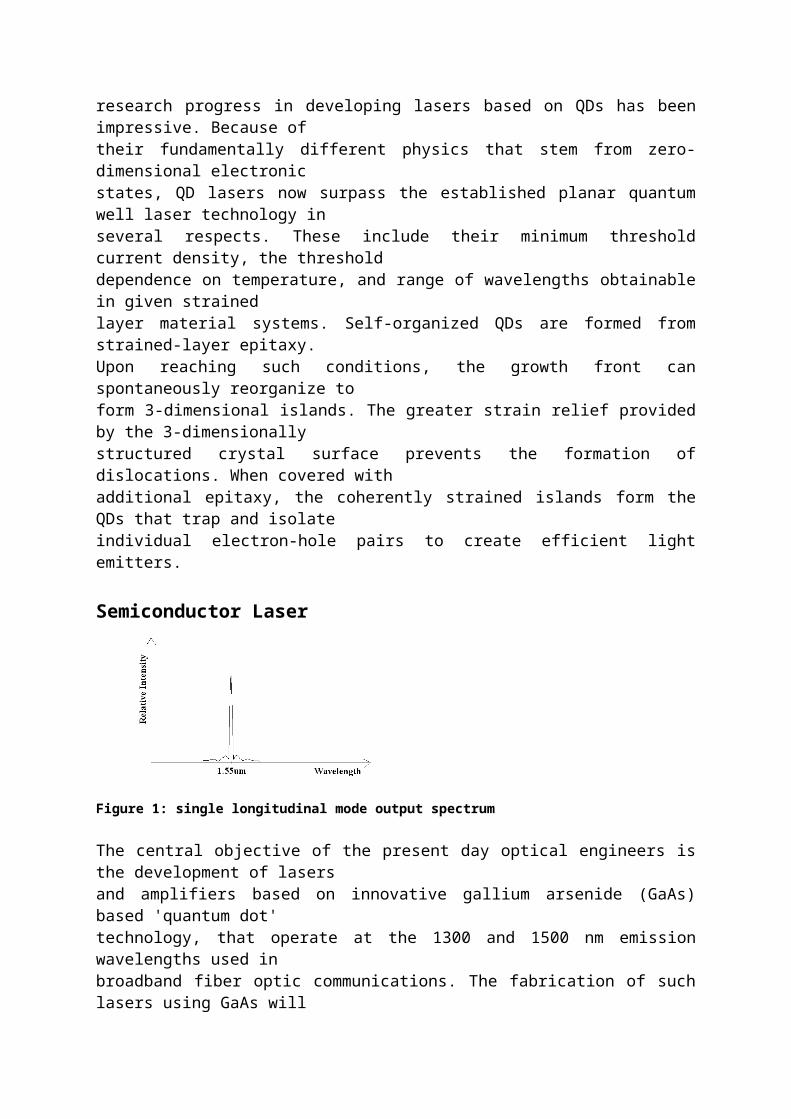
Figure 1: single longitudinal mode output spectrum
The central objective of the present day optical engineers is the development of lasersand amplifiers based on innovative gallium arsenide (GaAs) based 'quantum dot'technology, that operate at the 1300 and 1500 nm emission wavelengths used inbroadband fiber optic communications. The fabrication of such lasers using GaAs willdeliver a considerable cost advantage over the Indium Phosphide (InP) technologythat is currently the state-of-the-art for manufacturing devices at these wavelengths.The program is targeting the fabrication of quantum dots using standard and wellunderstood wafer fabrication systems.
The figure above shows a typical single longitudinal mode output spectrum from asingle mode injection laser. Single mode injection lasers are lasers that transmit asingle mode of radiation. Maximum relative intensity is obtained at a wavelength of
1.55μm, which is also the permitted wavelength for optoelectronic communication.Low optical loss and low dispersion of light can be achieved at this wavelength. LowHydroxyl loss in the optical fiber cable can also be obtained at this wavelength. Hencethis wavelength is of considerable importance and all the optical engineers are tryingto develop a laser having the same characteristics.
Quantum Dots
Optimizing the QD characteristics for use as practical, commercial light sources isbased on controlling their density, shape, and uniformity during epitaxy. In particular,the QD's shape plays a large role in determining its dynamic response, as well as thetemperature sensitivity of the laser's characteristics. Their density, shape, anduniformity also establish the optical gain of a QD ensemble. All three physicalcharacteristics can be engineered through the precise deposition conditions in whichtemperature, growth rate, and material composition are carefully controlled.Thus, the challenge in realizing quantum dot lasers with operation superior to thatshown by quantum well lasers is that of forming high quality, uniform quantum dotsin the active layer. The most widely followed approach to forming quantum dots wasthrough electron beam lithography of suitably small featured patterns (~300 Å) andsubsequent dry-etch transfer of dots into the substrate material. The problem thatplagued these quantum dot arrays was their exceedingly low optical efficiency: highsurface-to-volume ratios of these nanostructures and associated high surfacerecombination rates, together with damage introduced during the fabrication itself,precluded the successful formation of a quantum dot laser.
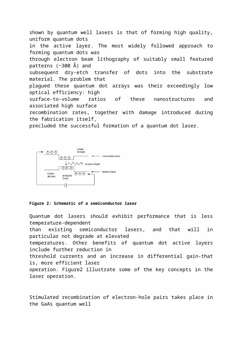
Figure 2: Schematic of a semiconductor laser
Quantum dot lasers should exhibit performance that is less temperature-dependentthan existing semiconductor lasers, and that will in particular not degrade at elevatedtemperatures. Other benefits of quantum dot active layers include further reduction inthreshold currents and an increase in differential gain-that is, more efficient laseroperation. Figure2 illustrate some of the key concepts in the laser operation.
Stimulated recombination of electron-hole pairs takes place in the GaAs quantum wellregion, where the confinement of carriers and of the optical mode enhances theinteraction between carriers and radiation. The population inversion (creation ofelectrons and holes) necessary for lasing occurs more efficiently as the active layermaterial is scaled down from bulk (3-dimensional) to quantum dots (0-dimensional).However, the advantages in operation depend not only on the absolute size of thenanostructures in the active region, but also on the uniformity of size. A broaddistribution of sizes "smears" the density of states, producing behavior similar to thatof bulk material.
Quantum dots (QDs) make up the structure of a material at maximum quantization.When the space, at any side, around a material shrinks to 100Å (one millionth cm),quantization of the energy levels at the reduced side will occur. Comparing with bulk,quantum well is one-dimensionally quantized, quantum wire being two-dimensionally

quantized, and QD is three-dimensionally quantized. However, from the threedimensionalperspective, the order of dimensionality of the three is reversed: quantumwell being two-dimensional, quantum wire one-dimensional, and QD being zerodimensional.
When quantization reaches its maximum, the energy levels of QDs are highlydiscontinuous. Theoretically, under such a condition, electrons in the energy levelshave the least sensitivity to temperature changes. Thus, QDs should produce lasers ofbetter quality than that of quantum well and quantum wire. Another advantage of aQD laser is that they can be turned on at very low threshold current. Not only is thepotential of a QD amazing, it is also important to the studies of fundamental physics.
Given that research on QDs has become rather popular around the world, it is notsurprising that QDs will play a critical role in the nanotechnology of the 21th century.However, with further advances in the understanding and development of QD lasers,we may see that much of the future laser diode technology convert to this zerodimensionalactive region, similar to the conversion in the last 10 years to planarquantum wells from bulk material.
Figure 3. Atomic force microscope images showing the control of theQD density using a strained buffer layer. (a) shows InGaAs QDs

grown directly on GaAs, and the QD density is ~1010 cm-2. (b) showssimilar InGaAs QDs grown with a strained layer buffer, whichincreases the QD density to ~2x~1010 cm-2.
The atomic force microscope images shown in Fig. 3 illustrate how a strained bufferlayer can be used to control the density of InGaAs QDs. In Fig. 3 (a) the InGaAs QDsare deposited directly on GaAs, and alternating depositions of In, Ga, and As are usedto achieve high surface atom mobility and slow growth rates to form the efficient 1.3μm QD emitters. Their density is ~1010 cm-2. In Fig. 3 (b) the same strained-layerdeposition is performed on a thin, strained InGaAs buffer layer of less In content, andthe QD density increases to ~2x1010 cm-2. The increase in the QD densitysignificantly improves laser performance. Because of the novel physics associatedwith the QD ensemble, the active material shown in Fig. 3 (b) has resulted in thelowest threshold current density yet reported (19 A/cm2) for any semiconductormaterial system for continuous-wave (CW) room temperature operation. Even lowerthreshold current densities could be possible in the future. At a slightly lowertemperature of ~200 K the threshold current density of the InGaAs QD material ofFig. 2 (b) reduces to 5 A/cm2, and generates lasers with threshold currents of ~400μA.
The interest in quantum dots was initially driven by a desire to create a material withelectronic density of states strongly modified by quantum confinement effects (areduction in size to less than tens of nanometers) and approaching a delta-like densityof states for a truly zero-dimensional system. Such a medium was perceived to offersignificant advantages for example in ultra-low threshold semiconductor diode lasers,

and also presented interesting opportunities for fundamental research in the area oflight-matter interaction.
In the self-assembled growth the quantum dots are created from ultrathin layers(typically about 2 monolayers thick) which spontaneously break up due to strainbetween the substrate and the grown film, and minimize their energy by formingsmall scale islands. Size quantization in such islands has been demonstrated.Self-assembled growth has proven to be an extremely fruitful technique which is nowwidely used. At Macquarie University scientists have made significant advances inmaterial growth and understanding of the self-assembly growth process and itscontrol. We deposit GaSb quantum dots on GaAs using atmospheric pressuremetalorganic chemical vapour deposition. The GaSb dots (islands) self-organise dueto lattice mismatch of several percent between GaAs and GaSb. The dots can bevisualised using a technique called Atomic Force Microscopy producing photographicimages.
Studies of quantum dots attract significant interest worldwide, because of theirFascinating new physics and unique potential for innovative electronic andOptoelectronic devices. Actually, these innovative applications are just beginning toemerge. One of them involves using quantum dots for the detection of infrared lightin devices similar to the previously explored quantum well intersubband detectors.
Other interesting applications include use in quantum gates at the centre of a quantumcomputer.
Devices being investigated utilise both standard and non-standard bandedge profilesand are being used as transmission and reflection irradiance modulators. Individualmodulators are being combined into the common self electro-optic effect device

(SEED) configuration for implementation of logical functions. The operation ofsymmetric SEED's is being investigated for application to optical oversampledanalog-to-digital conversion applications.
The figure shown in here is the pictorial representation of the GaSb, which is thecounterpart of the conventional GaAs structures which is the mai subject that has beendealt in the seminar and a whole lot of information is given in the coming sections.The aim of the research on GaSb quantum dots was to establish a technology tofabricate a three dimensional quantum dot composite material, a building block forfuture electronic and optoelectronic devices. This is achieved by depositing multiplelayers of quantum dots interspersed with quantum barriers of a different material.
Interestingly, the dots show some degree of vertical correlation.A lure demonstration of feasibility of QD growth using atmospheric pressureMOCVD can be easily expained using the GaSb structures. This is significant,because of an extremely rapid turnover time possible in such systems. Scientistsworking in the university could complete the growth process (from loading thechamber to taking the sample out) within 1 hour, while the actual QD growth takesseveral seconds. Such short times indicate a process which may be industriallyrelevant.
Theory of GaInNAs materials and optoelectronics devices:
GaInNAs exhibits a remarkable band-gap bowing, enabling optical emission at 1.3and 1.5 microns on a GaAs substrate. The first theory which explains qualitativelyand quantitatively the origin of this strong bowing in bulk GaInNAs has beendeveloped. The theory is based on and confirmed by tight-binding calculations that

have been performed. The model will be validated and refined by comparison withexperimental data from collaborators and from the literature. Calculations will then beundertaken to investigate how the unique features of GaInNAs/GaAs quantum wellschange laser gain characteristics compared to conventional GaInAsP/InP andAlGaInAs/InP QW lasers. These unique features include an extremely largeconduction band offset, comparable conduction and valence effective masses, andsignificantly reduced optical transition matrix elements, due to strong mixing with anN-related resonance level. Our modelling provides the first clear understanding of theelectronic properties of GaInNAs materials, and will enable us to predict optimumGaInNAs quantum-well laser structures
Assessment of InGaAsN materials and optoelectronic devices:
The III-V alloy InGaAsN shows quite remarkable band structure properties that raiseexciting possibilities for optoelectronic applications. Although GaN has a much largerband gap than GaAs, when a low concentration of N is incorporated into GaAs thereis a very strong decrease in the optical band gap. This is very interesting boththeoretically and practically: theoretically, because the behaviour cannot be explainedby standard models of III-V alloys and so new approaches are clearly needed;practically, because the lower band gap makes accessible in the GaAs system the1.3um and 1.55um wavelengths of interest for optical fibre communications. If wecan achieve a good theoretical understanding of the band structure and opticalproperties of InGaAsN, the possibility exists that we may be able to propose noveland superior optoelectronic device structures, (eg with mc*=mv*). To temperaturedependences of I. The optical and electrical properties of InGaAsN/GaAs quantumwells and II. The gain and loss processes in laser diodes. The results will be used to

refine our new theoretical model which then will be used to predict optimum laserstructures.
Long wavelength quantum dot lasers
Trunk communications using silica optical fibres at 1.55um have grown enormouslyin recent years. However, all 1.55um lasers are very temperature sensitive and requireexpensive control modules. Therefore, if such systems are to be extended into thehome and into the workplace, cheaper, simpler to operate devices are required. InAson InP quantum dots promise lasers ideal for this purpose. This proposal aims todevelop these devices starting from basic growth through to working laser diodes.Edge-emitting lasers will be fabricated and studied in detail using a variety ofexperimental and theoretical techniques developed recently at Surrey for 1.55umquantum well lasers. This will involve novel high pressure and low temperaturetechniques.
Theoretical models will address1) the electronic band structure including strain effects2) radiative and non-radiative transitions and optical gain,3) the waveguide structure and lasing characteristics.
Self-organized QDs based on strained layer epitaxy have pushed semiconductor lasersnearly to the ultimate in terms of their quantum dimensionality. Lasing is obtainedfrom truly zero-dimensional energy levels, and the novel quantum physics andnanostructure material features open new avenues for future semiconductor laserdevice research and development. Through use of microcavities, new types of lightemitters and lasers can be envisioned that also make use of a zero-dimensional photonfield. QD lasers exhibit both important new performance features that are unmatchedby previous semiconductor lasers based on planar quantum wells or bulk active

materials that include ultra-low threshold current densities, regimes of temperatureinsensitive lasing, reduction of the linewidth enhancement factor, and a greater rangeof lasing wavelengths for a given material system. On the other hand, they also haveproblems that must be overcome to advance to the status of commercial products,such as their small room temperature modulation bandwidth and poor temperaturesensitivity above room temperature.
1.3 μm InGaAs QD Lasers and Selective Oxidation
The central objective is the development of lasers and amplifiers based on innovativegallium arsenide (GaAs) based 'quantum dot' technology, that operate at the 1300 and1500 nm emission wavelengths used in broadband fiber optic communications. Thefabrication of such lasers using GaAs will deliver a considerable cost advantage overthe Indium Phosphide (InP) technology that is currently the state-of-the-art formanufacturing devices at these wavelengths. The program is targeting the fabricationof quantum dots using standard and well understood wafer fabrication systems.
Quantum dots (QDs) are nanometer-sized objects that are fabricated by deposition ofa thin semiconductor layer on a substrate with a different lattice constant (a materialstechnology generally known as compound semiconductors). Due to their smalldimensions, QDs confine trapped carriers in all three spatial directions, combining theadvantages of semiconductors with the defined behaviour of atoms. This supports thecreation of novel optical communications devices with very stable performance thatare much less prone to problems suffered by today's devices, such as distortion.
A wealth of studies on InGaAs QDs now show that the emission wavelength in 3-dimensionally, coherently-strained III-V epitaxy can be extended well beyond that

possible with 2-dimensionally coherently strained heterostructures of the samematerials. This feature has been convincingly demonstrated with GaAs-based InGaAsQD lasers that operate beyond 1.3 μm wavelength that now operate at CW thresholdcurrents close to 1 mA and threshold current densities less than 20 A/cm2. Thedevelopment of long-wavelength nano-structured materials could lead to GaAs- basedlight sources that cover the entire wavelength range of ~0.7 μm to beyond 1.55 μmimportant for data-communication and telecommunication technologies. Creation of aphonon bottleneck in the QDs might also be used to significantly reduce thresholdsfor intraband quantum-cascade lasers that operate in the 10 μm to 20 μm wavelengthrange.

Figure 4. (a) Schematic illustration of the oxide-confined QD laser.Two oxide layers have been placed 0.25 μm above and below thewaveguide layer, and the laser uses a single InGaAs QD activeregion with a ground state emission at 1.3 μm. (b) Lasingcharacteristics of the 1.3 μm, oxide-defined QD laser.
An advantage of 1.3 μm GaAs-based lasers is their ability to be oxidized to form

buried low refractive index insulators. An example is shown in Fig. 4, where theselective oxidation scheme for planar quantum well edge-emitting semiconductorlasers are applied to a 1.3 μm InGaAs QD laser. The oxide simultaneously channelselectrical current due to electron-hole injection into the laser's active region, andlaterally confines photons of the lasing mode. Figure 4 (b) shows that this type oflaser can operate at low CW, room temperature power levels with threshold currentsapproaching 1 mA. More recent results show that 1.3 μm QD lasers can exhibitcharacteristic temperatures as high as 80 K even above 300 K. The 80 K characteristictemperature exceeds that of commercial InP-based 1.3 μm lasers, so that 1.3 μmGaAs-based QD lasers may eventually compete with commercial InP-based lasers.
Shape-Engineering and Control of the QD Electronic Structure
A major limitation in today's QD lasers is poor temperature performance at and aboveroom temperature. In the presence of inhomogeneous broadening, ground state QDlasers can potentially offer a characteristic threshold temperature, commonly calledTo, of several hundred Kelvin at wavelengths of 1.3 μm and beyond. This is well inexcess of planar quantum well InP-based lasers. The temperature insensitive thresholdhas been measured in several studies for below room temperature operation of QDlasers.
With the work described here, QDs are formed using strained layer epitaxy of InAs ona GaAs surface in which a 7% lattice mismatch exists between the 2 materials. Asmall amount of strained material can be grown while maintaining dislocation freeplanar surface this is called pseudomorphic growth. When a critical thickness issurpassed, the 3-D islands form spontaneously in order to reduce the surface free

energy of the strained material. Some strained 2-D material remains after theformation of the QDs and is called the wetting layer. The critical thickness isdependent upon the lattice mismatch, growth temperature, and other growthcondition. Interestingly, the modified optical properties also can arise in largernanostructures (that is not quantised in the growth plane) due to stress gradients in thequantum dots, these lead to normal incidence operation of quantum dot lightdetectors.
However, even in QDs thermal excitation of electrons and holes can occur to higherenergy levels associated with either zero-dimensional states of the QD or the QDwetting layer. Thermal excitation to the wetting layer is a particularly seriousproblem, because of the wetting layer's relatively large density of levels. Therefore,the best room temperature performance has been obtained with InGaAs QDs that havedeep potential wells, with ground state light emission beyond 1.2 μm. Since thesedeep QDs are also typically rather large (several hundred angstroms in diameter), theycontain multiple discrete electron and hole levels. For the deep QDs, these higherenergy zero-dimensional quantum states in large part control the lasers thresholdsensitivity to temperature. For the 1.3 μm InGaAs QDs, the energy separationbetween the ground and first excited radiative transitions is ~66 meV.
By engineering the QD shape to be narrow in lateral size, the ground state energy canstill be deep with respect to the wetting layer, but also have a wide energy separationbetween the ground and first excited radiative transitions.
The temperature dependence of the lasing threshold for both a 1.3 μm InGaAs QDlaser and a 1.24 μm InAs QD laser are shown in Fig. 5. Some differences in the laserstructures give different minimum threshold currents for low temperatures, and the

1.3 μm InGaAs QD laser reaches lower threshold current density at low temperature.However, the difference at room temperature and above is set mainly by the energyseparation between the ground and first excited radiative transitions. The QD'selectronic levels also control its dynamic response. Larger QDs show shorterspontaneous lifetimes at low temperatures, and very fast capture times. Manyexperimental studies attempting to characterize capture times for electrons and holeshave been flawed by transport time delays of charge carriers. However, more accurateexperiments are now being performed, and show that larger QDs can respond fasterthan smaller QDs in both their capture time and spontaneous emission rate. Initialexperiments on the QD modulation response suggest that QD lasers are slower thanplanar quantum well lasers at room temperature, but become comparable in speedbelow room temperature. The precise reasons are not yet known, and show that thereis much research yet to be done on QD lasers to fully understand and optimize theirperformance.
An increasing need for sources and detectors for mid and far infrared applicationssuch as infrared spectroscopy for chemical analysis, remote sensing and atmosphericcommunications provides the driving force to develop improved infrared lightdetectors. At present, commercial infrared light detectors are principally based onHgCdTe, and while their performance parameters such as detectivity and responsivityremain excellent, their deficiencies such as nonuniformity of HgCdTe wafers,important for imaging, as well as difficult manufacturing technology remain well

Figure 5. Plot of threshold current density versus temperaturefor either a 1.3 μm InGaAs QD laser, or a 1.24 μm InAs QDlasers. For room temperature operation and above, thetemperature dependence of the threshold current density is setby the energy separation between the ground and first excitedradiative transitions. These are ~66 meV for the InGaAs QDlaser, and ~104 meV for the InAs QD laser.
known. Therefore the motivation arose to seek alternatives, preferably based onGaAs-type materials where advanced growth technology such as the molecular beamepitaxy (MBE) is widely available. Since over ten years the quantum wellintersubband detectors (QWIPS) based on GaAs-type materials are being developed,and while this work still continues, much of the underlying science has been wellestablished.
Because the InGaAs QDs form self-buried heterostructures, they are ideal for use withthe most sophisticated III-V laser device processing aimed at microcavity devices.The ability to convert high Al content AlGaAs layer to oxide makes the GaAs-basedAlGaAs/GaAs/InGaAs strained layer QD system ideal for microcavities. Such devicesoffer an unprecedented control over a spontaneous emitter's lifetime through themechanism known as the Purcell effect. The Purcell effect is generated by phasecoherent

electromagnetic feedback due to closely spaced reflecting boundaries. Thereflecting boundaries both modify the amplitudes of the quantum fluctuations thatexist in the electromagnetic field and drive the spontaneous emitter, as well as theamplitude of the emitter's radiated spontaneous field. Either increase (or decrease) theemitter's spontaneous emission rate by equal amounts. Because the phase-coherencetime is short for spontaneous emission, microcavities are required that place theelectromagnetic reflectors as close as possible to the light emitter.
As the size of the microcavity shrinks, the control over both the directionality and therate of the spontaneous emission increases. The directionality is strongly dependenton the microcavity geometry. Fabry-Perot type microcavities can radiate a collimated,single lobed beam, and therefore achieve high efficiency coupling with the simplestoptical interconnects. Figure 6 shows the emission characteristics from such a QDoxide-confined microcavity when the QDs are inhomogeneously broadened. Themicrocavity is formed by selectively oxidizing AlGaAs layers, as shown in the inset,to form an intracavity aperture of approximately 1 μm diameter. The QDs that emit onresonance with the micro- cavity show a spontaneous emission rate that is increasedby 250 % over those QDs that emit at wavelengths either shorter or longer than themicrocavity resonance peak. Other reports based on etched-pillar microcavities showup to 500 % lifetime change for the smallest pillar sizes. Because the increase in thespontaneous emission rate can be used to fabricate high speed, high efficiency lasers,as well as extremely low power high efficiency spontaneous light emitters, this typeof QD microcavity technology may be useful for ultra-low power opticalinterconnects and displays. Microarrays of high efficiency microcavity light emittersmay also compete with higher power VCSELs and light emitting diodes.
Recently, new fundamental optical properties of nanostructures have been discovered.

These include significant changes in the energy level assignment and in the selectionrules for optical absorption. The relaxed selection rules, and particularly absorption atnormal incidence (forbidden in most commonly used n-type GaAs/AlGaAs quantumwells.
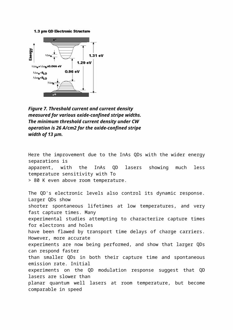
An energy level diagram for 1.3 μm InGaAs QDs is illustrated in Fig. 7. In nearly allIII-V semiconductor self-organized QD's reported to date, the height of the QD ismuch less than its lateral dimension. Along with the In composition, the height andlateral dimension establish important traits of the QD electronic structure. Due toquantum size effects, the height mainly sets the energy difference between the wettinglayer and the ground state and the lateral size mainly sets the energy separationsbetween the ground and higher energy radiative transitions due to discrete levels.Figure 8 shows electroluminescence from InAs QDs designed for such wide energyseparations. As measured by atomic force microscope, their lateral size is ~250 Å.Figure 8 shows that the small lateral size results in an energy separation between theground and first excited radiative transition of 104 meV. The ground state emissionwavelength is ~1.24 μm. The energy separation between the ground and first excitedradiative transitions is the largest yet reported for InAs or InGaAs QDs.

Figure 7. Threshold current and current densitymeasured for various oxide-confined stripe widths.The minimum threshold current density under CWoperation is 26 A/cm2 for the oxide-confined stripewidth of 13 μm.
Here the improvement due to the InAs QDs with the wider energy separations isapparent, with the InAs QD lasers showing much less temperature sensitivity with To> 80 K even above room temperature.
The QD's electronic levels also control its dynamic response. Larger QDs showshorter spontaneous lifetimes at low temperatures, and very fast capture times. Manyexperimental studies attempting to characterize capture times for electrons and holeshave been flawed by transport time delays of charge carriers. However, more accurateexperiments are now being performed, and show that larger QDs can respond fasterthan smaller QDs in both their capture time and spontaneous emission rate. Initialexperiments on the QD modulation response suggest that QD lasers are slower thanplanar quantum well lasers at room temperature, but become comparable in speedbelow room temperature. The precise reasons are not yet known, and show that thereis much research yet to be done on QD lasers to fully understand and optimize theirperformance.
Figure 8. Spontaneous emission spectrum for an InAs QD

light emitter engineered to have wide energy separationsbetween the discrete radiative transitions.
Quantum Dots in the world of OptoelectroniccommunicationQuantum dots (QDs) make up the structure of a material at maximum quantization.When the space, at any side, around a material shrinks to 100Å (one millionth cm),quantization of the energy levels at the reduced side will occur. Comparing with bulk,quantum well is one-dimensionally quantized, quantum wire being two-dimensionallyquantized, and QD is three-dimensionally quantized. However, from the threedimensionalperspective, the order of dimensionality of the three is reversed :quantum well being two-dimensional, quantum wire one-dimensional, and QD beingzero dimensional.
When quantization reaches its maximum, the energy levels of QDs are highlydiscontinuous. Theoretically, under such a condition, electrons in the energy levelshave the least sensitivity to temperature changes. Thus, QDs should produce lasers ofbetter quality than that of quantum well and quantum wire. Another advantage of aQD laser is that they can be turned on at very low threshold current. Not only is thepotential of a QD amazing, it is also important to the studies of fundamental physics.
Given that research on QDs has become rather popular around the world, it is notsurprising that QDs will play a critical role in the nanotechnology of the 21st century.
Traditionally, network communication relied on copper cables, with both data loadingand transmission being limited. Today, it is being replaced by fiber optic cable. Forthe latter, signal transmissions rely mainly on optical waves produced by lasers.
Accordingly, lasers are becoming increasingly important in the era of fiber opticcommunication. Transmission in optical fiber has the lowest loss at wavelengths of1.31μm and 1.55 μm, allowing fiber optic signal transmission to reach its maximumdistance. Thus, the Opto-Electronics & Systems Laboratories (OES) research group,has emphasized its research on producing long wavelength lasers longer than 1 μm.In the recent two years the quantum dot infrared detectors emerged at the forefront oflight detector research, In comparison with QWIPS, the quantum dot detectors offerimportant advantages in regard to the performance parameters such as responsivity,detectivity and normal incidence operation. Standard quantum dot detectors, similarlyto QWIPs respond to a single radiation wavelength or to a narrow spectral band.
Shortcomings of InGaAsP
The ultimate goal of each research teams is, of course, to provide the industry with acost-effective solution and yet a feasible one using the most appropriate material andtechnology to grow lasers. The currently matured technology for lasers used in fiberoptic communication involves the growth of InGaAsP edge-emitting lasers andvertical cavity surface emitting lasers (VCSEL) using InP substrate. However, twoproblems inherent to the InGaAsP lasers need to be addressed : poor temperaturestability and low efficiency of the reflective mirrors made. For the latter, analternative is to use the AlGaAs series for reflecting mirrors instead, and couple itwith the InGaAsP active region through wafer bonding. This will obviously increasethe complication in wafer manufacturing and therefore the cost. This, coupled withthe low temperature stability, has aroused a vast search for new materials. "QDs is oneof the technologies to replace InGaAsP. Another is the use of InGaNAs with 1-2% ofnitrogen".

Advantages of QDs
"Laser requires a high temperature-stability so that it will not burn out whenoverheated. QD lasers are exactly the tool which could overcome the disadvantages ofInGaAsP", said Dr. Chang. "Theoretically, a QD laser has a very high temperaturestability.It can also be grown directly on GaAs substrate, making use of the AlGaAsdistributed Bragg reflector (DBR) in one single growth without the need of waferbonding technique."The central objective is the development of lasers and amplifiers based on innovativegallium arsenide (GaAs) based 'quantum dot' technology, that operate at the 1300 and1500 nm emission wavelengths used in broadband fiber optic communications. Thefabrication of such lasers using GaAs will deliver a considerable cost advantage overthe Indium Phosphide (InP) technology that is currently the state-of-the-art formanufacturing devices at these wavelengths. The program is targeting the fabricationof quantum dots using standard and well understood wafer fabrication systems.
Due to their small dimensions, QDs confine trapped carriers in all three spatialdirections, combining the advantages of semiconductors with the defined behaviour ofatoms. This supports the creation of novel optical communications devices with verystable performance, that are much less prone to problems suffered by today's devices,such as distortion Development of quantum dot lasers on GaAs substrates for the 980nm and 1.3 μm wavelength range. While in the 980 nm wavelength range theemphasis is more on high power applications and single mode emitting lasers suitablefor gas sensoric, the interest for 1.3 μm emitting quantum dot lasers is in therealization of low cost but high performance devices for optical communication whichcan eventually substitute InP based devices in future. Beside the extension of the

wavelength range of the GaAs based material system quantum dot specific featureswill be investigated which can improve device functions as e.g. low threshold current,improved modulation behavior, reduced temperature sensitivity, reducedfilamentation and mirror load for high power applications, etc..
Development of quantum dot lasers on GaAs substrates for the 980 nm and 1.3 μmwavelength range. While in the 980 nm wavelength range the emphasis is more onhigh power applications and single mode emitting lasers suitable for gas sensoric, theinterest for 1.3 μm emitting quantum dot lasers is in the realization of low cost buthigh performance devices for optical communication which can eventually substitute
InP based devices in future. Beside the extension of the wavelength range of the GaAsbased material system quantum dot specific features will be investigated which canimprove device functions as e.g. low threshold current, improved modulationbehavior, reduced temperature sensitivity, reduced filamentation and mirror load forhigh power applications, etc.
It has therefore been anticipated that the success achieved in using quantum wellstructures in novel optoelectronic and electronic devices may be extended by usingquantum dots instead of quantum wells due to significant improvements in theInfrared detector performance. The significance of quantum dot light detectors lies inthe fact that they are an emerging class of infrared detectors that will complement theHgCdTe detectors and QWIPs with commensurate or higher detectivity and fastresponse time. HgCdTe are traditionally the only high detectivity far infrared detectoron the market today. Investigations of quantum dot light detectors have just started toappear in the recent literature. These devices offer scope for improved performancecompared to quantum well light detector devices (QWIPs), and hence they aresignificant, while relatively unexplored

The modified properties of quantum dots significantly influence the key light detectorparameters, such as detectivity and responsivity. Compared to quantum wells used inQWIPs, quantum dots are characterised by slowing of the intersubband relaxationtime due to a reduced electron-phonon interaction. The reduced phonon scatteringdue to a discrete density of states in a quantum dot leads to long lifetime and longdephasing time and therefore to an increased radiative efficiency. Quantum dotdetectors are also expected to exhibit lower dark current and noise than a quantumwell detector.
Research on GaSb quantum dots was to establish a technology to fabricate a threedimensional quantum dot composite material, a building block for future electronicand optoelectronic devices. This is achieved by depositing multiple layers of quantumdots interspersed with quantum barriers of a different material. Interestingly, the dotsshow some degree of vertical correlation. Identification and understanding of growthevolution was possible. The systematic studies of growth evolution with variation ofgrowth parameters indicate a variety of different scenarios, where the dilution ofprecursors and the growth time both play a role, in addition to the commonlyrecognized influences of growth temperature and the lattice mismatch. Opticalcharacterization and analysis of optical emission is the added advantage. Inembedded films we have observed optical (photoluminescence andcathodoluminescence) emission at energies about 1.0 eV, with peak energiesfollowing the trend in dot sizes. We interpret this by a combined effect of quantumconfinement and interface intermixing. Hence comparison of GaSb dots embedded inGaAs with an opposite system of GaAs embedded in GaSb, and with a II-VI systemof ZnTe dots in CdSe was possible.

Quantum Dot Research - the future nowThe remaining major division of the field of quantum electronics deals with theinteractions of coherent light with matter and again leads to a wide range of all-opticaland opto-electronic devices.
Advances in research into the quantum dot phenomena made by scientists at IMShave resulted in a recent article in Nature Magazine and have attracted internationalrecognition.
The research, a collaboration between IMS and the University of Wurzburg, has led tothe ability to probe a single quantum dot and gradually increase the number ofelectrons and holes populating it. This is equivalent to creating artificial atoms andbuilding a man-made periodic table.
By carefully controlling the excitation, the scientists were able to study the interactionof many electrons and holes (excitons), observing the difference in their emissionspectra and providing important insight into the physics of such quantum systems.
The nanostructures confining carriers will play a crucial role in future technologieswith the miniaturization of semiconductor devices for electronics and photonicsapplications. . A more distant hope is the application of QDs in improved opticalmemory. GaN has a much larger band gap than GaAs and very expectant researchesare going on the GaN and its alloys. When a low concentration of N is incorporatedinto GaAs there is a very strong decrease in the optical band gap. This is veryinteresting both theoretically and practically: theoretically, because the behaviourcannot be explained by standard models of III-V alloys and so new approaches areclearly needed; practically, because the lower band gap makes accessible in the GaAssystem the 1.3um and 1.55um wavelengths of interest for optical fibre

communications. If we can achieve a good theoretical understanding of the bandstructure and optical properties of InGaAsN, the possibility exists that we may be ableto propose novel and superior optoelectronic device structures.
CONCLUSION
The infrastructure of the Information Age has to date relied upon advances inmicroelectronics to produce integrated circuits that continually become smaller,better, and less expensive. Traditionally, network communication relied on coppercables, with both data loading and transmission being limited. Today, it is beingreplaced by fiber optic cable. For the latter, signal transmissions rely mainly onoptical waves produced by lasers. Accordingly, lasers are becoming increasinglyimportant in the era of fiber optic communication. The remaining major division ofthe field of quantum electronics deals with the interactions of coherent light withmatter and again leads to a wide range of all-optical and optoelectronic devices.
Transmission in optical fiber has the lowest loss at wavelengths of 1.31μm and 1.55μm, allowing fiber optic signal transmission to reach its maximum distance.The emergence of photonics, where light rather than electricity is manipulated, isposed to further advance the Information Age. Central to the photonic revolution isthe development of miniature light sources such as the QDs. Today, QDsmanufacturing has been established to serve new datacom and telecom markets.
Recent progress in microcavity physics, new materials, and fabrication technologieshas enabled a new generation of high performance QDs. This presentation hasreviewed commercial QDs and their applications as well as recent researches,including new device structures such as applications of 3-dimensional QD arrays.

For the any industry interested in entering fiber optical communication, being able togrow LED, is only the first step; the next will be producing edge-emitting lasers andthen QDS and VCSELs. For the benefits of the domestic industry, now is the time tostart R&D effort on the long wavelength QDs lasers. Due to the optimized growthapproach, sub-monolayer deposits results in large, low density QDs. Besides 1.3 umemission wavelength, QDs demonstrate very low threshold current density due to lowtransparency current and low free-carrier absorption and temperatre-insenseitivethreshold due to deep confinement potentials with large energy separation betweenstates. This principle is used in the opto-electronic communication.