V7AZ to V1000 Replacement Manual - mcabv.nl · PDF fileV7AZ to V1000 Replacement Instructions...
30
YASKAWA Electric Europe GmbH Drives Engineering Section Page 1 of 30 YASKAWA ―― Contents ―― 1 Concerned Drives .............................................................................................................. 2 2 Drive Replacement Checklist............................................................................................. 3 3 Terminals ........................................................................................................................... 5 3.1 Main circuit terminals ................................................................................................ 7 3.2 Control Terminals, Signal Levels .............................................................................. 8 3.3 Serial communications terminals .............................................................................. 9 3.4 DIP Switches ............................................................................................................ 9 3.5 Terminal Size/ Electric Wire Differences ................................................................... 9 3.6 Control terminal sizes and wire sizes ..................................................................... 12 4 Dimensions, installation space and substitution material ................................................. 12 4.1 IP20 Type ............................................................................................................... 12 4.2 NEMA Type 1.......................................................................................................... 13 5 Options Replacement ...................................................................................................... 14 6 Parameter Correspondence Table ................................................................................... 15 6.1 V7AZ→V1000 Parameter Correspondence for Drive Replacement .................... 15 6.2 V7AZ and V1000 Differences in Parameter Settings 7 V7AZ and V1000 differences in rated power, current and carrier frequency.................... 29 Revision History .................................................................................................................... 30 V7AZ to V1000 Replacement Instructions
Transcript of V7AZ to V1000 Replacement Manual - mcabv.nl · PDF fileV7AZ to V1000 Replacement Instructions...
YASKAWA Electric Europe GmbH Drives Engineering Section
Page 1 of 30
YASKAWA
―― Contents ――
1 Concerned Drives..............................................................................................................2 2 Drive Replacement Checklist.............................................................................................3 3 Terminals ...........................................................................................................................5
3.1 Main circuit terminals ................................................................................................7 3.2 Control Terminals, Signal Levels ..............................................................................8 3.3 Serial communications terminals ..............................................................................9 3.4 DIP Switches ............................................................................................................9 3.5 Terminal Size/ Electric Wire Differences ...................................................................9 3.6 Control terminal sizes and wire sizes .....................................................................12
4 Dimensions, installation space and substitution material.................................................12 4.1 IP20 Type ...............................................................................................................12 4.2 NEMA Type 1..........................................................................................................13
5 Options Replacement ......................................................................................................14 6 Parameter Correspondence Table...................................................................................15
6.1 V7AZ→V1000 Parameter Correspondence for Drive Replacement ....................15 6.2 V7AZ and V1000 Differences in Parameter Settings
7 V7AZ and V1000 differences in rated power, current and carrier frequency....................29 Revision History ....................................................................................................................30
V7AZ to V1000 Replacement Instructions
YASKAWA Electric Europe GmbH Drives Engineering Section
Page 2 of 30
YASKAWA Concerned Drives
This document describes the substitution of the following drives: Original drive: CIMR-V7AZxxxx , Spec: xxxx0 (IP20) or xxxx1 (NEMA1) Software Version S5740 or S5750 Replacement: CIMR-VZAxxxxxxx This description is not valid for drives with other specs or other firmware installed!
Main Differences
• V1000 has only 6 inputs, S7 not available • Analog input A1 in V1000 does not accept 4-20mA use A2 instead • V1000 has 2nd analog input on standard terminals (A2) • Operator panel is not detachable in V1000 • Operator and Memobus communication (RJ45, RS232) are possible at the
same time on V1000 • No potentiometer in the operator panel use up/down keys for local reference instead • Torque detection always compares to torque in vector control. N097 is not necessary
anymore V1000 vector control has better performance. • Scaling for memobus frequency monitor independent from display is not possible. (n152) • Input and Output Open phase detection does not have direct correspondence
n166/n167/n168/n169 • No DC braking PI available in V1000 (n173/n174). Not necessary anymore in V1000. • Sequence Input redundent reading n143 is not necessary anymore in V1000 (faster scan)
YASKAWA Electric Europe GmbH Drives Engineering Section
Page 3 of 30
YASKAWA Drive Replacement Checklist
Item Checkpoints Checked?
< Check the installation type > ∗ Check if the drive is installed with the heat sink put through the
panel wall. For heat sink outside installation a special mounting kit is
necessary. Refer to part 0 of this manual for finding the appropriate mounting kit.
∗ Check if the new drive dimensions are not bigger than the old ones. V1000 up to 4kW has same mounting dimensions. Use part 0 of this manual to compare the sizes of the old
and new unit. In case that a mechanical substitution kit is necessary, it is mentioned there.
< Digital operator panel > ∗ Does the digital operator panel need to be at the same position
as before? If necessary try to readjust the position in order to have the
operator panel at the same location as before. ∗ Was a remote operator panel connected to the old unit?
If so, never connect the old remote operator panel to the V1000. Replace existing remote operators by the new type. See part 0 of this manual for options replacement.
Basic
< Special specifications > ∗ Check the installed drives specification to make sure, that it is
compliant to the standard specification (no special firmware, no special coating, no special brand ...)
< Wire Length > ∗ In the replacement drive the main and control circuit terminals
can be at a different position. Check if all cables are long enough to be connected without tension to the new unit.
Hardware
Main and control
terminals < Main circuit wires and terminal specifications> ∗ Compare the occupied terminals of the old unit with the new
drives terminals (shape, size, etc.) and check if the wires fit in the new units terminals using part 0 of this book.
Software Software version
< Check for special software > ∗ Check the software number in the old unit to be sure, that no
special software is used. If necessary ask your dealer to find out, if the installed
software on the old unit is a special software or not. If the old drive has a special software installed, it might not be easily possible to replace it with a V1000.
Software Parameter
< Check the parameter settings> ∗ Read out the parameter settings of the old unit and perform a
parameter transformation to the new parameters following part 0 of this book.
∗ If there is a special software installed or parameters, which are not mentioned in this book appear, contact your dealer.
YASKAWA Electric Europe GmbH Drives Engineering Section
Page 4 of 30
YASKAWA
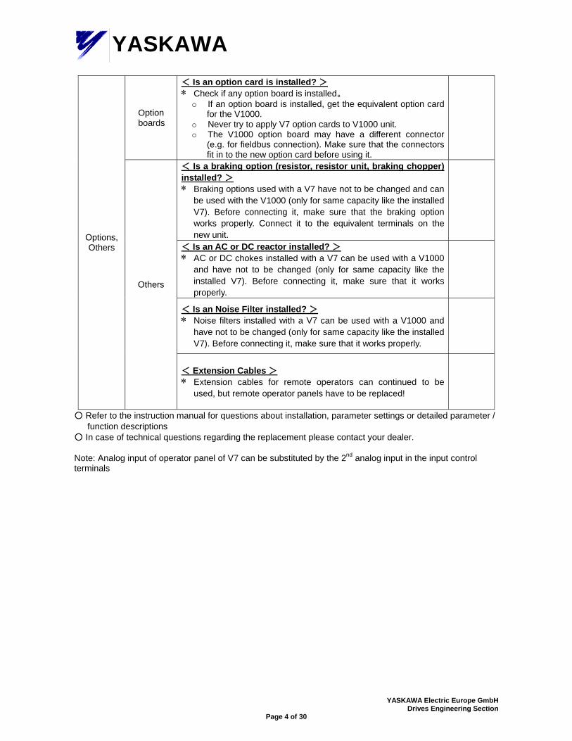
Option boards
< Is an option card is installed? > ∗ Check if any option board is installed。
If an option board is installed, get the equivalent option card for the V1000.
Never try to apply V7 option cards to V1000 unit. The V1000 option board may have a different connector
(e.g. for fieldbus connection). Make sure that the connectors fit in to the new option card before using it.
< Is a braking option (resistor, resistor unit, braking chopper) installed? > ∗ Braking options used with a V7 have not to be changed and can
be used with the V1000 (only for same capacity like the installed V7). Before connecting it, make sure that the braking option works properly. Connect it to the equivalent terminals on the new unit.
< Is an AC or DC reactor installed? > ∗ AC or DC chokes installed with a V7 can be used with a V1000
and have not to be changed (only for same capacity like the installed V7). Before connecting it, make sure that it works properly.
< Is an Noise Filter installed? > ∗ Noise filters installed with a V7 can be used with a V1000 and
have not to be changed (only for same capacity like the installed V7). Before connecting it, make sure that it works properly.
Options, Others
Others
< Extension Cables > ∗ Extension cables for remote operators can continued to be
used, but remote operator panels have to be replaced!
○ Refer to the instruction manual for questions about installation, parameter settings or detailed parameter / function descriptions
○ In case of technical questions regarding the replacement please contact your dealer. Note: Analog input of operator panel of V7 can be substituted by the 2nd analog input in the input control terminals
YASKAWA Electric Europe GmbH Drives Engineering Section
Page 5 of 30
YASKAWAV7AZ Connecting Diagram
24V
24C
S6
S5
S4
S3
S2
S1
SCPNP
NPNSW1
RP
FS
FR
FC
S+
S-
R+
R-
IGTerminal Resistance (120O ,1/ 2W)
R/ L1
S/ L2
T/ L3
Main Circuit Power Supply Single-phase power supply uses R/L1 and S/L2
+2 +1 - B1 B2
u x
DC Reactor (Option)
Braking Resistor (Option)
Short Circuit
Main Contactor
Forward Run/ Stop
Reverse Run/ Stop
External Fault (N.O.)
Fault Reset
Multi-Step Speed Cmd 1
Multi-Step Speed Cmd 2
U/ T1
V/ T2
W/ T3
IM
Ground
MA
MB
MC
Fault
P1
P2
PC
During Run
Frequency Agree
AM
AC
+
-
Multi-Func. Input
Main Speed Freq Cmd
Pulse Train Input
Frequency Setting Device
2kO p
p
Pulse Train Input(Max 33kHz)
Frequency Setting Power Supply +10V / max. 20mAMain Speed Freq Ref
0 to +10V(20kO )4 to 20mA / 0 to 20mA (250O )
Multi-Function Photo-Coupler Output DC48V / 50mA
Multi-Function Digital Output AC250V / 1A DC30V / 1A
AM
Analog Monitor Output DC0 to +10V(2mA)
Memobus Comm. RS-485/ 422max 19,2 kbps
p
Shielded connection terminal
Shielded
p
p
L1
L2
L3
LineFilter
(option)
PE
S7Jog Command
Detachable Operator with potentiometer for local reference
(selected by SW2-2)
SW2-1p Twisted pair cable
YASKAWA Electric Europe GmbH Drives Engineering Section
Page 6 of 30
YASKAWAV1000 Connecting Diagram
YASKAWA Electric Europe GmbH Drives Engineering Section
Page 7 of 30
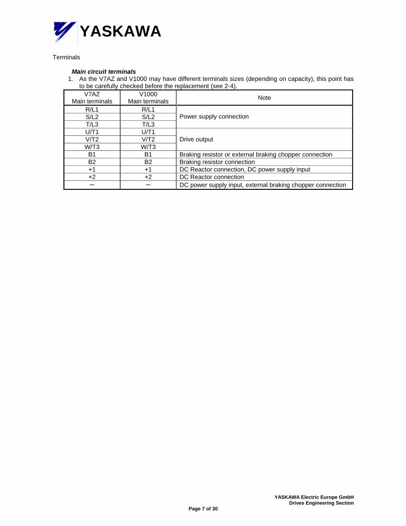
YASKAWATerminals
Main circuit terminals 1. As the V7AZ and V1000 may have different terminals sizes (depending on capacity), this point has
to be carefully checked before the replacement (see 2-4). V7AZ
Main terminals V1000
Main terminals Note
R/L1 R/L1 S/L2 S/L2 T/L3 T/L3
Power supply connection
U/T1 U/T1 V/T2 V/T2 W/T3 W/T3
Drive output
B1 B1 Braking resistor or external braking chopper connection B2 B2 Braking resistor connection +1 +1 DC Reactor connection, DC power supply input +2 +2 DC Reactor connection - - DC power supply input, external braking chopper connection
YASKAWA Electric Europe GmbH Drives Engineering Section
Page 8 of 30
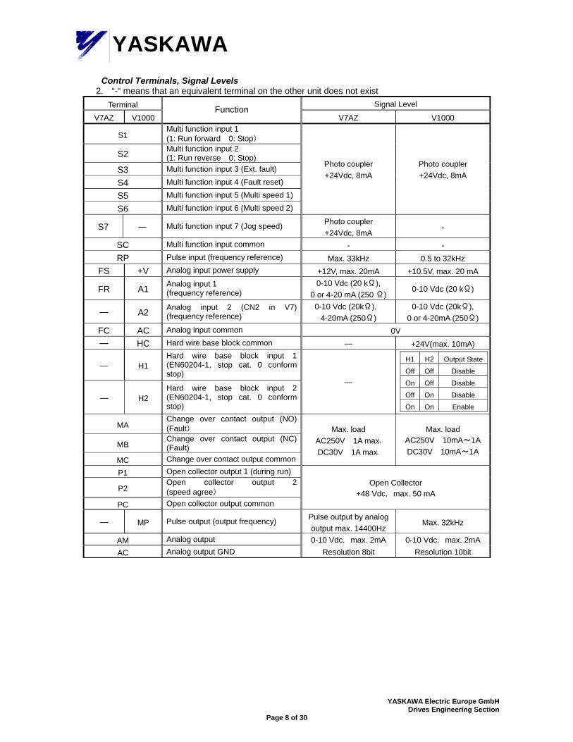
YASKAWAControl Terminals, Signal Levels
2. “-“ means that an equivalent terminal on the other unit does not exist Terminal Signal Level
V7AZ V1000 Function
V7AZ V1000
S1 Multi function input 1 (1: Run forward 0: Stop)
S2 Multi function input 2 (1: Run reverse 0: Stop)
S3 Multi function input 3 (Ext. fault)
S4 Multi function input 4 (Fault reset)
S5 Multi function input 5 (Multi speed 1)
S6 Multi function input 6 (Multi speed 2)
Photo coupler +24Vdc, 8mA
Photo coupler +24Vdc, 8mA
S7 ― Multi function input 7 (Jog speed) Photo coupler +24Vdc, 8mA
-
SC Multi function input common - - RP Pulse input (frequency reference) Max. 33kHz 0.5 to 32kHz
FS +V Analog input power supply +12V, max. 20mA +10.5V, max. 20 mA
FR A1 Analog input 1 (frequency reference)
0-10 Vdc (20 kΩ), 0 or 4-20 mA (250 Ω)
0-10 Vdc (20 kΩ)
― A2 Analog input 2 (CN2 in V7)(frequency reference)
0-10 Vdc (20kΩ), 4-20mA (250Ω)
0-10 Vdc (20kΩ), 0 or 4-20mA (250Ω)
FC AC Analog input common 0V ― HC Hard wire base block common ― +24V(max. 10mA)
― H1 Hard wire base block input 1 (EN60204-1, stop cat. 0 conform stop)
― H2 Hard wire base block input 2 (EN60204-1, stop cat. 0 conform stop)
―
H1 H2 Output State
Off Off Disable
On Off Disable
Off On Disable
On On Enable
MA Change over contact output (NO) (Fault)
MB Change over contact output (NC) (Fault)
MC Change over contact output common
Max. load AC250V 1A max. DC30V 1A max.
Max. load AC250V 10mA~1A DC30V 10mA~1A
P1 Open collector output 1 (during run)
P2 Open collector output 2 (speed agree)
PC Open collector output common
Open Collector +48 Vdc,max. 50 mA
― MP Pulse output (output frequency) Pulse output by analog output max. 14400Hz
Max. 32kHz
AM Analog output
AC Analog output GND 0-10 Vdc,max. 2mA
Resolution 8bit 0-10 Vdc,max. 2mA
Resolution 10bit
YASKAWA Electric Europe GmbH Drives Engineering Section
Page 9 of 30
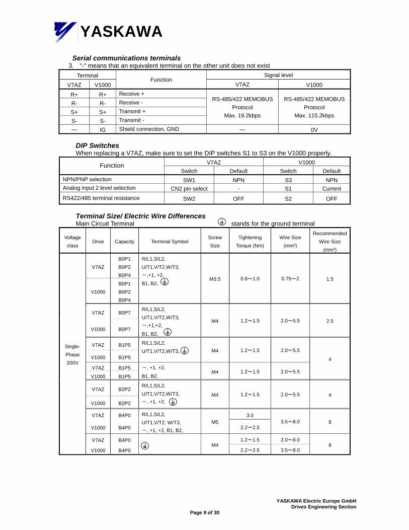
YASKAWASerial communications terminals
3. “-“ means that an equivalent terminal on the other unit does not exist Terminal Signal level
V7AZ V1000 Function
V7AZ V1000
R+ R+ Receive +
R- R- Receive -
S+ S+ Transmit +
S- S- Transmit -
RS-485/422 MEMOBUS Protocol
Max. 19.2kbps
RS-485/422 MEMOBUS Protocol
Max. 115.2kbps
― IG Shield connection, GND ― 0V DIP Switches When replacing a V7AZ, make sure to set the DIP switches S1 to S3 on the V1000 properly.
V7AZ V1000 Function Switch Default Switch Default
NPN/PNP selection SW1 NPN S3 NPN Analog input 2 level selection CN2 pin select - S1 Current RS422/485 terminal resistance SW2 OFF S2 OFF
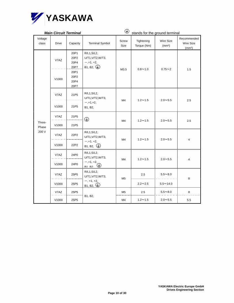
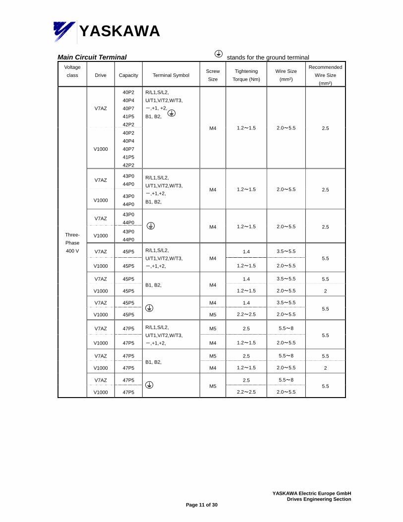
Terminal Size/ Electric Wire Differences Main Circuit Terminal stands for the ground terminal
Voltage class
Drive Capacity Terminal Symbol Screw Size
Tightening Torque (Nm)
Wire Size (mm²)
Recommended Wire Size
(mm²)
V7AZ B0P1 B0P2 B0P4
V1000 B0P1 B0P2 B0P4
R/L1,S/L2, U/T1,V/T2,W/T3, -,+1, +2,
B1, B2, M3.5 0.8~1.0 0.75~2 1.5
V7AZ B0P7
V1000 B0P7
R/L1,S/L2, U/T1,V/T2,W/T3,-,+1,+2,
B1, B2,
M4 1.2~1.5 2.0~5.5 2.5
V7AZ B1P5
V1000 B1P5
R/L1,S/L2, U/T1,V/T2,W/T3,
M4 1.2~1.5 2.0~5.5
V7AZ B1P5
V1000 B1P5
-, +1, +2,
B1, B2, M4 1.2~1.5 2.0~5.5
4
V7AZ B2P2
V1000 B2P2
R/L1,S/L2, U/T1,V/T2,W/T3, -, +1, +2,
M4 1.2~1.5 2.0~5.5 4
V7AZ B4P0 3.0
V1000 B4P0
R/L1,S/L2, U/T1,V/T2, W/T3, -, +1, +2, B1, B2,
M5 2.2~2.5
3.5~8.0 8
V7AZ B4P0 1.2~1.5 2.0~8.0
Single- Phase 200V
V1000 B4P0
M4
2.2~2.5 3.5~8.0 8
YASKAWA Electric Europe GmbH Drives Engineering Section
Page 10 of 30
YASKAWA Main Circuit Terminal stands for the ground terminal
Voltage class Drive Capacity Terminal Symbol
Screw Size
Tightening Torque (Nm)
Wire Size (mm²)
Recommended Wire Size
(mm²)
V7AZ
20P1 20P2 20P4 20P7
V1000
20P1 20P2 20P4 20P7
R/L1,S/L2, U/T1,V/T2,W/T3, -,+1, +2,
B1, B2, M3.5 0.8~1.0 0.75~2 1.5
V7AZ 21P5
V1000 21P5
R/L1,S/L2, U/T1,V/T2,W/T3,-,+1,+2,
B1, B2,
M4 1.2~1.5 2.0~5.5 2.5
V7AZ 21P5
V1000 21P5
M4 1.2~1.5 2.0~5.5 2.5
V7AZ 22P2
V1000 22P2
R/L1,S/L2, U/T1,V/T2,W/T3, -,+1, +2,
B1, B2,
M4 1.2~1.5 2.0~5.5 4
V7AZ 24P0
V1000 24P0
R/L1,S/L2, U/T1,V/T2,W/T3, -,+1, +2,
B1, B2,
M4 1.2~1.5 2.0~5.5 4
V7AZ 25P5 2.5 5.5~8.0
V1000 25P5
R/L1,S/L2, U/T1,V/T2,W/T3, -, +1, +2,
B1, B2,
M5
2.2~2.5 5.5~14.0
8
V7AZ 25P5 M5 2.5 5.5~8.0 8
Three- Phase 200 V
V1000 25P5 B1, B2,
M4 1.2~1.5 2.0~5.5 5.5
YASKAWA Electric Europe GmbH Drives Engineering Section
Page 11 of 30
YASKAWA Main Circuit Terminal stands for the ground terminal
Voltage class Drive Capacity Terminal Symbol
Screw Size
Tightening Torque (Nm)
Wire Size (mm²)
Recommended Wire Size
(mm²)
V7AZ
40P2 40P4 40P7 41P5 42P2
V1000
40P2 40P4 40P7 41P5 42P2
R/L1,S/L2, U/T1,V/T2,W/T3, -,+1, +2,
B1, B2,
M4 1.2~1.5 2.0~5.5 2.5
V7AZ 43P0 44P0
V1000 43P0 44P0
R/L1,S/L2, U/T1,V/T2,W/T3, -,+1,+2,
B1, B2,
M4 1.2~1.5 2.0~5.5 2.5
V7AZ 43P0 44P0
V1000 43P0 44P0
M4 1.2~1.5 2.0~5.5 2.5
V7AZ 45P5 1.4 3.5~5.5
V1000 45P5
R/L1,S/L2, U/T1,V/T2,W/T3, -,+1,+2,
M4 1.2~1.5 2.0~5.5
5.5
V7AZ 45P5 1.4 3.5~5.5 5.5
V1000 45P5 B1, B2, M4
1.2~1.5 2.0~5.5 2
V7AZ 45P5 M4 1.4 3.5~5.5
V1000 45P5
M5 2.2~2.5 2.0~5.5 5.5
V7AZ 47P5 M5 2.5 5.5~8
V1000 47P5
R/L1,S/L2, U/T1,V/T2,W/T3, -,+1,+2, M4 1.2~1.5 2.0~5.5
5.5
V7AZ 47P5 M5 2.5 5.5~8 5.5
V1000 47P5 B1, B2,
M4 1.2~1.5 2.0~5.5 2
V7AZ 47P5 2.5 5.5~8
Three- Phase 400 V
V1000 47P5
M5
2.2~2.5 2.0~5.5 5.5
YASKAWA Electric Europe GmbH Drives Engineering Section
Page 12 of 30
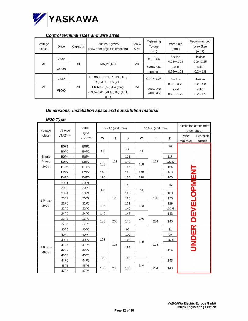
YASKAWAControl terminal sizes and wire sizes
Voltage class
Drive Capacity Terminal Symbol
(new or changed in brackets) Screw Size
Tightening Torque (Nm)
Wire Size (mm²)
Recommended Wire Size
(mm²)
V7AZ 0.5~0.6
All
V1000
All MA,MB,MC M3 Screw less terminals
flexible 0.25~1.25
solid 0.25~1.25
flexible 0.2~1.25
solid 0.2~1.5
V7AZ 0.22~0.25
All V1000
All
S1-S6, SC, P1, P2, PC, R+, R-, S+, S-, FS (V+),
FR (A1), (A2) ,FC (AC), AM,AC,RP, (MP), (HC), (H1),
(H2)
M2 Screw less terminals
flexible 0.25~0.75
solid 0.25~1.25
flexible 0.2~1.0
solid 0.2~1.5
Dimensions, installation space and substitution material
IP20 Type
V7AZ (unit: mm) V1000 (unit: mm) Installation attachment
(order code) Voltage class
V7 type V7AZ****
V1000 Type
VZA**** W H D W H D Panel
mounted Heat sink outside
B0P1 B0P1
B0P2 B0P2 76
76
B0P4 B0P4
68
131
68
118
B0P7 B0P7 140 137.5
B1P5 B1P5 108
156 108
154
B2P2 B2P2 140 163 140 163
Single Phase 200V
B4P0 B4P0 170
128
180 170
128
180
20P1 20P1
20P2 20P2 76 76
20P4 20P4 108 108
20P7 20P7
68
128
68
128
21P5 21P5 131 129
22P2 22P2 108
140 108
137.5
24P0 24P0 140
128
143
128
143
25P5 25P5
3 Phase 200V
27P5 27P5 180 260 170
140 234 140
40P2 40P2 92 81
40P4 40P4 110 99
40P7 40P7 140 137.5
41P5 41P5
42P2 42P2
108
156
43P0 43P0
108
154
44P0 44P0 140
128
143
128
143
45P5 45P5
3 Phase 400V
47P5 47P5 180 260 170
140 234 140
U
ND
ER D
EVEL
OPM
ENT
YASKAWA Electric Europe GmbH Drives Engineering Section
Page 13 of 30
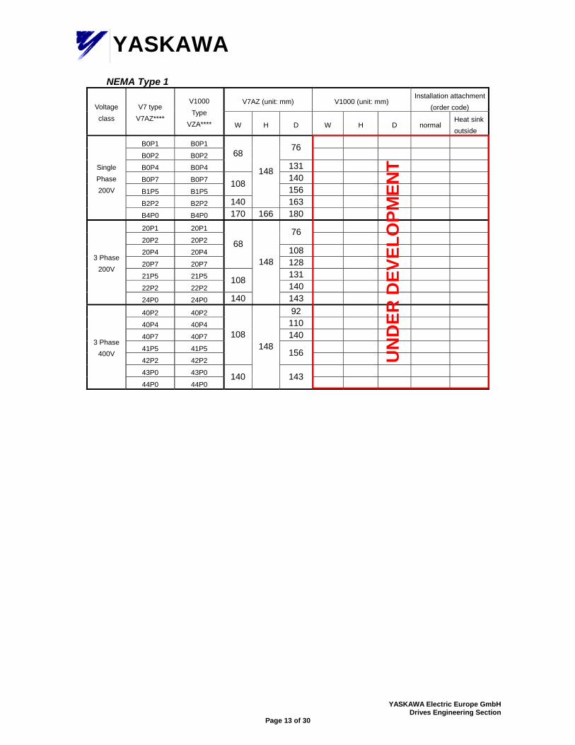
YASKAWANEMA Type 1
V7AZ (unit: mm) V1000 (unit: mm) Installation attachment
(order code) Voltage class
V7 type V7AZ****
V1000 Type
VZA**** W H D W H D normal Heat sink outside
B0P1 B0P1
B0P2 B0P2 76
B0P4 B0P4
68 131
B0P7 B0P7 140
B1P5 B1P5 108
156
B2P2 B2P2 140
148
163
Single Phase 200V
B4P0 B4P0 170 166 180
20P1 20P1
20P2 20P2 76
20P4 20P4 108
20P7 20P7
68
128
21P5 21P5 131
22P2 22P2 108
140
3 Phase 200V
24P0 24P0 140
148
143
40P2 40P2 92
40P4 40P4 110
40P7 40P7 140
41P5 41P5
42P2 42P2
108
156
43P0 43P0
3 Phase 400V
44P0 44P0 140
148
143
U
ND
ER D
EVEL
OPM
ENT
YASKAWA Electric Europe GmbH Drives Engineering Section
Page 14 of 30
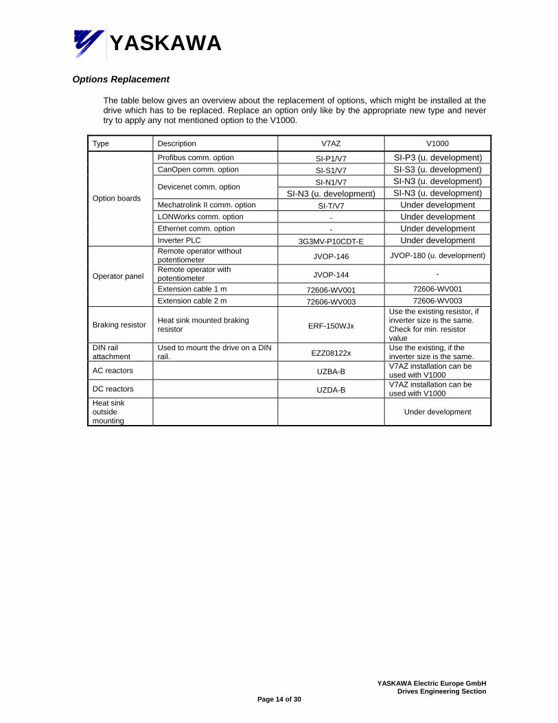
YASKAWAOptions Replacement
The table below gives an overview about the replacement of options, which might be installed at the drive which has to be replaced. Replace an option only like by the appropriate new type and never try to apply any not mentioned option to the V1000.
Type Description V7AZ V1000
Profibus comm. option SI-P1/V7 SI-P3 (u. development) CanOpen comm. option SI-S1/V7 SI-S3 (u. development)
SI-N1/V7 SI-N3 (u. development) Devicenet comm. option
SI-N3 (u. development) SI-N3 (u. development) Mechatrolink II comm. option SI-T/V7 Under development LONWorks comm. option - Under development Ethernet comm. option - Under development
Option boards
Inverter PLC 3G3MV-P10CDT-E Under development Remote operator without potentiometer JVOP-146 JVOP-180 (u. development)
Remote operator with potentiometer JVOP-144 -
Extension cable 1 m 72606-WV001 72606-WV001 Operator panel
Extension cable 2 m 72606-WV003 72606-WV003
Braking resistor Heat sink mounted braking resistor ERF-150WJx
Use the existing resistor, if inverter size is the same. Check for min. resistor value
DIN rail attachment
Used to mount the drive on a DIN rail. EZZ08122x
Use the existing, if the inverter size is the same.
AC reactors UZBA-B V7AZ installation can be used with V1000
DC reactors UZDA-B V7AZ installation can be used with V1000
Heat sink outside mounting
Under development
YASKAWA Electric Europe GmbH Drives Engineering Section
Page 15 of 30
YASKAWAParameter Correspondence Table
V7AZ→V1000 Parameter Correspondence for Drive Replacement 4. Before setting up other parameters, make sure that C6-01 is set to “0”. 5. The given voltage values are valid for 200 V units. For 400 V units the values have to be doubled. 6. The given V1000 defaults for max. frequency are given for European spec (o2-09 = 2)
V7AZ V1000 Drive Function/ Parameter
Parameter No.
Initial Value Parameter
No. Initial Value
Comments
Parameter access level A1-01 2
Initialization A1-03 0 RUN command In PRG mode select b1-08 0
Fault history U2,U3 initialization
001 1
o4-04 0
V7AZ V1000 n001→0 A1-01→0
n001→1~4 A1-01→2
n001→5 A1-01→2 b1-08→1
n001→6 o4-11→1 n001→12 A1-03→2220 n001→13 A1-03→3330
Control mode selection 002 0 A1-02 2 V7AZ V1000
n002→0 A1-02→0 n002→1 A1-02→2
RUN command source selection 003 0 b1-02 1
V7AZ V1000 n003→0 b1-02→0 n003→1 b1-02→1 n003→2 b1-02→2 n003→3 b1-02→3
Frequency reference source selection 004 0 b1-01 1
Frequency reference by analog input A2 (signal level) selection
004 078
0 1
H3-09 2
V7AZ V1000 n004→0 - n004→1 b1-01→0
n004→2 b1-01→1 and if Term. A1: H3-01→0 if Term. A2: H3-09→0
n004→3 Term. A2: b1-01→1 and H3-09→2
n004→4 Term. A2: b1-01→1 and H3-09→3
n004→5 b1-01→4 n004→6 b1-01→2
n004→7n078→0
b1-01→1 and if Term. A1: H3-01→0 if Term. A2: H3-09→0
n004→8n078→1
Term. A2: b1-01→1 and H3-09→2
n004→9 b1-01→3 To use an analog input as frequency reference, the input function must be set to 0 in parameter H3-02 or H3-10. When using A2 make sure to set DIP switch S1 properly.
Stop method selection 005 0 b1-03 0 V7AZ V1000
n005→0 b1-03→0 n005→1 b1-03→1
YASKAWA Electric Europe GmbH Drives Engineering Section
Page 16 of 30
YASKAWAV7AZ V1000 Drive
Function/ Parameter
Parameter No.
Initial Value Parameter
No. Initial Value
Comments
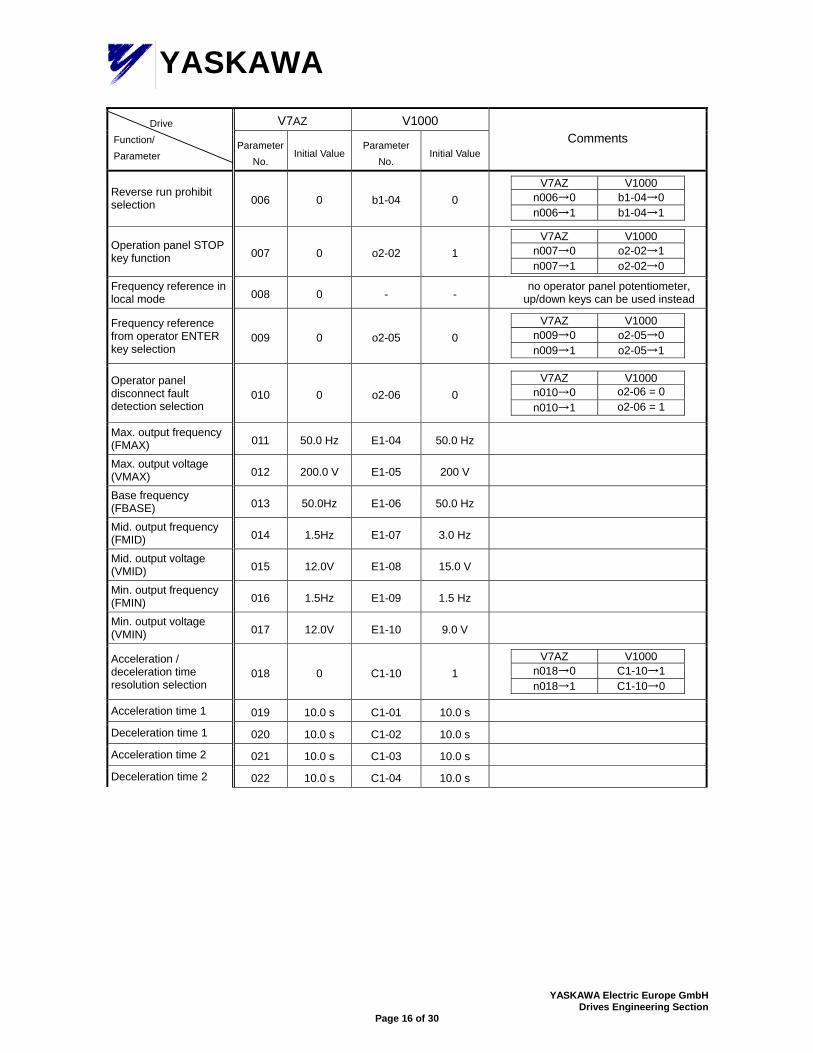
Reverse run prohibit selection 006 0 b1-04 0
V7AZ V1000 n006→0 b1-04→0 n006→1 b1-04→1
Operation panel STOP key function 007 0 o2-02 1
V7AZ V1000 n007→0 o2-02→1 n007→1 o2-02→0
Frequency reference in local mode 008 0 - -
no operator panel potentiometer, up/down keys can be used instead
Frequency reference from operator ENTER key selection
009 0 o2-05 0 V7AZ V1000
n009→0 o2-05→0 n009→1 o2-05→1
Operator panel disconnect fault detection selection
010 0 o2-06 0 V7AZ V1000
n010→0 o2-06 = 0 n010→1 o2-06 = 1
Max. output frequency (FMAX) 011 50.0 Hz E1-04 50.0 Hz
Max. output voltage (VMAX) 012 200.0 V E1-05 200 V
Base frequency (FBASE) 013 50.0Hz E1-06 50.0 Hz
Mid. output frequency (FMID) 014 1.5Hz E1-07 3.0 Hz
Mid. output voltage (VMID) 015 12.0V E1-08 15.0 V
Min. output frequency (FMIN) 016 1.5Hz E1-09 1.5 Hz
Min. output voltage (VMIN) 017 12.0V E1-10 9.0 V
Acceleration / deceleration time resolution selection
018 0 C1-10 1 V7AZ V1000
n018→0 C1-10→1 n018→1 C1-10→0
Acceleration time 1 019 10.0 s C1-01 10.0 s
Deceleration time 1 020 10.0 s C1-02 10.0 s
Acceleration time 2 021 10.0 s C1-03 10.0 s
Deceleration time 2 022 10.0 s C1-04 10.0 s
YASKAWA Electric Europe GmbH Drives Engineering Section
Page 17 of 30
YASKAWAV7AZ V1000 Drive
Function/ Parameter
Parameter No.
Initial Value Parameter
No. Initial Value
Comments
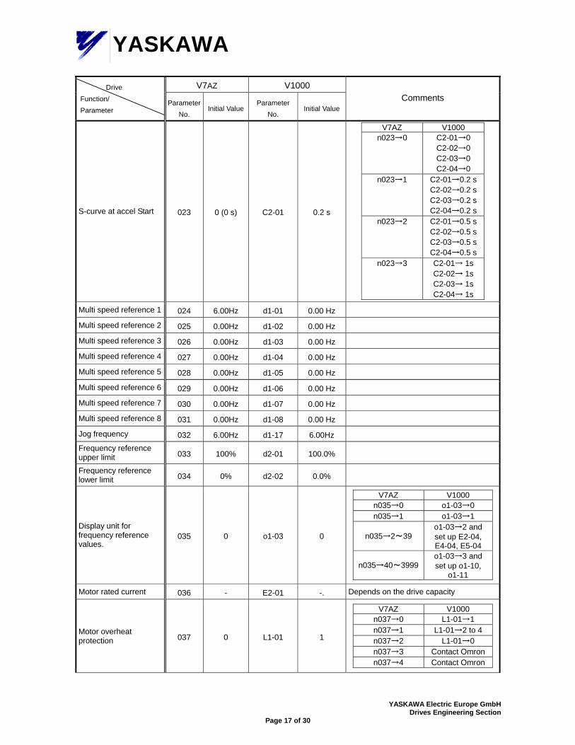
S-curve at accel Start 023 0 (0 s) C2-01 0.2 s
V7AZ V1000 n023→0 C2-01→0
C2-02→0 C2-03→0 C2-04→0
n023→1 C2-01→0.2 s C2-02→0.2 s C2-03→0.2 s C2-04→0.2 s
n023→2 C2-01→0.5 s C2-02→0.5 s C2-03→0.5 s C2-04→0.5 s
n023→3 C2-01→ 1s C2-02→ 1s C2-03→ 1s C2-04→ 1s
Multi speed reference 1 024 6.00Hz d1-01 0.00 Hz
Multi speed reference 2 025 0.00Hz d1-02 0.00 Hz
Multi speed reference 3 026 0.00Hz d1-03 0.00 Hz
Multi speed reference 4 027 0.00Hz d1-04 0.00 Hz
Multi speed reference 5 028 0.00Hz d1-05 0.00 Hz
Multi speed reference 6 029 0.00Hz d1-06 0.00 Hz
Multi speed reference 7 030 0.00Hz d1-07 0.00 Hz
Multi speed reference 8 031 0.00Hz d1-08 0.00 Hz
Jog frequency 032 6.00Hz d1-17 6.00Hz
Frequency reference upper limit 033 100% d2-01 100.0%
Frequency reference lower limit 034 0% d2-02 0.0%
Display unit for frequency reference values.
035 0 o1-03 0
V7AZ V1000 n035→0 o1-03→0 n035→1 o1-03→1
n035→2~39 o1-03→2 and set up E2-04, E4-04, E5-04
n035→40~3999 o1-03→3 and set up o1-10,
o1-11
Motor rated current 036 - E2-01 -. Depends on the drive capacity
Motor overheat protection 037 0 L1-01 1
V7AZ V1000 n037→0 L1-01→1 n037→1 L1-01→2 to 4 n037→2 L1-01→0 n037→3 Contact Omron n037→4 Contact Omron
YASKAWA Electric Europe GmbH Drives Engineering Section
Page 18 of 30
YASKAWAV7AZ V1000 Drive
Function/ Parameter
Parameter No.
Initial Value Parameter
No. Initial Value
Comments
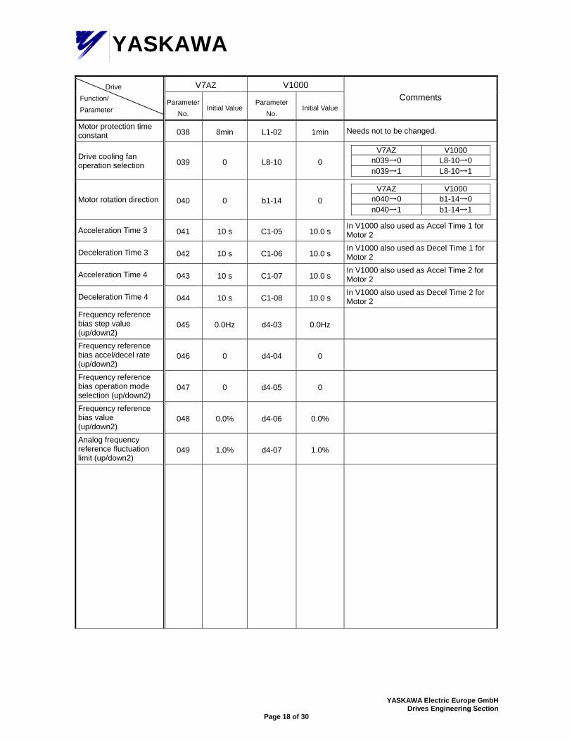
Motor protection time constant 038 8min L1-02 1min Needs not to be changed.
Drive cooling fan operation selection 039 0 L8-10 0
V7AZ V1000 n039→0 L8-10→0 n039→1 L8-10→1
Motor rotation direction 040 0 b1-14 0 V7AZ V1000
n040→0 b1-14→0 n040→1 b1-14→1
Acceleration Time 3 041 10 s C1-05 10.0 s In V1000 also used as Accel Time 1 for Motor 2
Deceleration Time 3 042 10 s C1-06 10.0 s In V1000 also used as Decel Time 1 for Motor 2
Acceleration Time 4 043 10 s C1-07 10.0 s In V1000 also used as Accel Time 2 for Motor 2
Deceleration Time 4 044 10 s C1-08 10.0 s In V1000 also used as Decel Time 2 for Motor 2
Frequency reference bias step value (up/down2)
045 0.0Hz d4-03 0.0Hz
Frequency reference bias accel/decel rate (up/down2)
046 0 d4-04 0
Frequency reference bias operation mode selection (up/down2)
047 0 d4-05 0
Frequency reference bias value (up/down2)
048 0.0% d4-06 0.0%
Analog frequency reference fluctuation limit (up/down2)
049 1.0% d4-07 1.0%
YASKAWA Electric Europe GmbH Drives Engineering Section
Page 19 of 30
YASKAWAV7AZ V1000 Drive
Function/ Parameter
Parameter No.
Initial Value Parameter
No. Initial Value
Comments
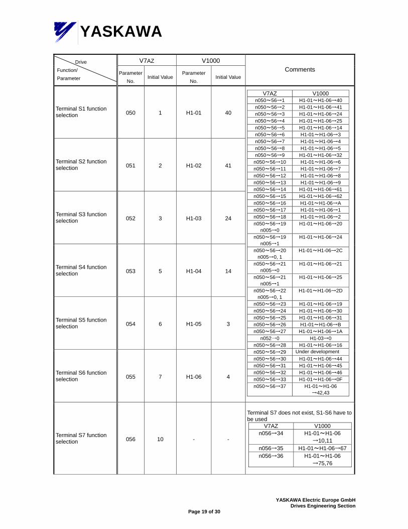
Terminal S1 function selection 050 1 H1-01 40
Terminal S2 function selection 051 2 H1-02 41
Terminal S3 function selection 052 3 H1-03 24
Terminal S4 function selection 053 5 H1-04 14
Terminal S5 function selection 054 6 H1-05 3
Terminal S6 function selection 055 7 H1-06 4
V7AZ V1000 n050~56→1 H1-01~H1-06→40 n050~56→2 H1-01~H1-06→41 n050~56→3 H1-01~H1-06→24 n050~56→4 H1-01~H1-06→25 n050~56→5 H1-01~H1-06→14 n050~56→6 H1-01~H1-06→3 n050~56→7 H1-01~H1-06→4 n050~56→8 H1-01~H1-06→5 n050~56→9 H1-01~H1-06→32
n050~56→10 H1-01~H1-06→6 n050~56→11 H1-01~H1-06→7 n050~56→12 H1-01~H1-06→8 n050~56→13 H1-01~H1-06→9 n050~56→14 H1-01~H1-06→61 n050~56→15 H1-01~H1-06→62 n050~56→16 H1-01~H1-06→A n050~56→17 H1-01~H1-06→1 n050~56→18 H1-01~H1-06→2 n050~56→19
n005→0 H1-01~H1-06→20
n050~56→19 n005→1
H1-01~H1-06→24
n050~56→20 n005→0, 1
H1-01~H1-06→2C
n050~56→21 n005→0
H1-01~H1-06→21
n050~56→21 n005→1
H1-01~H1-06→25
n050~56→22 n005→0, 1
H1-01~H1-06→2D
n050~56→23 H1-01~H1-06→19 n050~56→24 H1-01~H1-06→30 n050~56→25 H1-01~H1-06→31 n050~56→26 H1-01~H1-06→B n050~56→27 H1-01~H1-06→1A
n052→0 H1-03→0 n050~56→28 H1-01~H1-06→16 n050~56→29 Under development n050~56→30 H1-01~H1-06→44 n050~56→31 H1-01~H1-06→45 n050~56→32 H1-01~H1-06→46 n050~56→33 H1-01~H1-06→0F n050~56→37 H1-01~H1-06
→42,43
Terminal S7 function selection 056 10 - -
Terminal S7 does not exist, S1-S6 have to be used
V7AZ V1000 n056→34 H1-01~H1-06
→10,11 n056→35 H1-01~H1-06→67 n056→36 H1-01~H1-06
→75,76
YASKAWA Electric Europe GmbH Drives Engineering Section
Page 20 of 30
YASKAWAV7AZ V1000 Drive
Function/ Parameter
Parameter No.
Initial Value Parameter
No. Initial Value
Comments
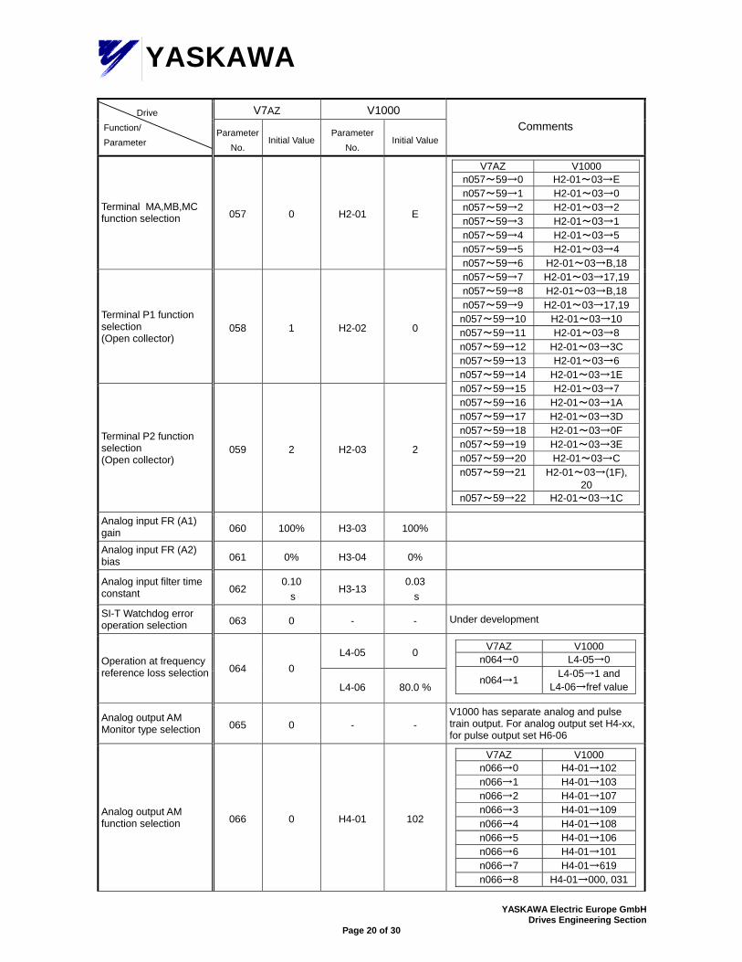
Terminal MA,MB,MC function selection 057 0 H2-01 E
Terminal P1 function selection (Open collector)
058 1 H2-02 0
Terminal P2 function selection (Open collector)
059 2 H2-03 2
V7AZ V1000 n057~59→0 H2-01~03→E n057~59→1 H2-01~03→0 n057~59→2 H2-01~03→2 n057~59→3 H2-01~03→1 n057~59→4 H2-01~03→5 n057~59→5 H2-01~03→4 n057~59→6 H2-01~03→B,18 n057~59→7 H2-01~03→17,19 n057~59→8 H2-01~03→B,18 n057~59→9 H2-01~03→17,19
n057~59→10 H2-01~03→10 n057~59→11 H2-01~03→8 n057~59→12 H2-01~03→3C n057~59→13 H2-01~03→6 n057~59→14 H2-01~03→1E n057~59→15 H2-01~03→7 n057~59→16 H2-01~03→1A n057~59→17 H2-01~03→3D n057~59→18 H2-01~03→0F n057~59→19 H2-01~03→3E n057~59→20 H2-01~03→C n057~59→21 H2-01~03→(1F),
20 n057~59→22 H2-01~03→1C
Analog input FR (A1) gain 060 100% H3-03 100%
Analog input FR (A2) bias 061 0% H3-04 0%
Analog input filter time constant 062
0.10 s
H3-13 0.03
s
SI-T Watchdog error operation selection 063 0 - - Under development
L4-05 0 Operation at frequency reference loss selection 064 0
L4-06 80.0 %
V7AZ V1000 n064→0 L4-05→0
n064→1 L4-05→1 and L4-06→fref value
Analog output AM Monitor type selection 065 0 - -
V1000 has separate analog and pulse train output. For analog output set H4-xx, for pulse output set H6-06
Analog output AM function selection 066 0 H4-01 102
V7AZ V1000 n066→0 H4-01→102 n066→1 H4-01→103 n066→2 H4-01→107 n066→3 H4-01→109 n066→4 H4-01→108 n066→5 H4-01→106 n066→6 H4-01→101 n066→7 H4-01→619 n066→8 H4-01→000, 031
YASKAWA Electric Europe GmbH Drives Engineering Section
Page 21 of 30
YASKAWAV7AZ V1000 Drive
Function/ Parameter
Parameter No.
Initial Value Parameter
No. Initial Value
Comments
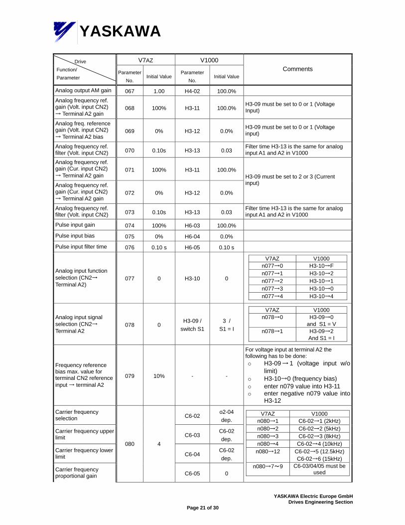
Analog output AM gain 067 1.00 H4-02 100.0%
Analog frequency ref. gain (Volt. input CN2) → Terminal A2 gain
068 100% H3-11 100.0% H3-09 must be set to 0 or 1 (Voltage Input)
Analog freq. reference gain (Volt. input CN2) → Terminal A2 bias
069 0% H3-12 0.0% H3-09 must be set to 0 or 1 (Voltage input)
Analog frequency ref. filter (Volt. input CN2) 070 0.10s H3-13 0.03
Filter time H3-13 is the same for analog input A1 and A2 in V1000
Analog frequency ref. gain (Cur. input CN2) → Terminal A2 gain
071 100% H3-11 100.0%
Analog frequency ref. gain (Cur. input CN2) → Terminal A2 gain
072 0% H3-12 0.0%
H3-09 must be set to 2 or 3 (Current input)
Analog frequency ref. filter (Volt. input CN2) 073 0.10s H3-13 0.03
Filter time H3-13 is the same for analog input A1 and A2 in V1000
Pulse input gain 074 100% H6-03 100.0%
Pulse input bias 075 0% H6-04 0.0%
Pulse input filter time 076 0.10 s H6-05 0.10 s
Analog input function selection (CN2→ Terminal A2)
077 0 H3-10 0
V7AZ V1000 n077→0 H3-10→F n077→1 H3-10→2 n077→2 H3-10→1 n077→3 H3-10→0 n077→4 H3-10→4
Analog input signal selection (CN2→ Terminal A2
078 0 H3-09 /
switch S1 3 /
S1 = I
V7AZ V1000 n078→0 H3-09→0
and S1 = V n078→1 H3-09→2
And S1 = I
Frequency reference bias max. value for terminal CN2 reference input → terminal A2
079 10% - -
For voltage input at terminal A2 the following has to be done: H3-09→ 1 (voltage input w/o
limit) H3-10→0 (frequency bias) enter n079 value into H3-11 enter negative n079 value into
H3-12
Carrier frequency selection C6-02
o2-04 dep.
Carrier frequency upper limit C6-03
C6-02 dep.
Carrier frequency lower limit C6-04
C6-02 dep.
Carrier frequency proportional gain
080 4
C6-05 0
V7AZ V1000 n080→1 C6-02→1 (2kHz) n080→2 C6-02→2 (5kHz) n080→3 C6-02→3 (8kHz) n080→4 C6-02→4 (10kHz) n080→12 C6-02→5 (12.5kHz)
C6-02→6 (15kHz) n080→7~9 C6-03/04/05 must be
used
YASKAWA Electric Europe GmbH Drives Engineering Section
Page 22 of 30
YASKAWAV7AZ V1000 Drive
Function/ Parameter
Parameter No.
Initial Value Parameter
No. Initial Value
Comments
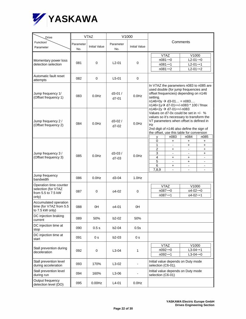
Momentary power loss detection selection 081 0 L2-01 0
V7AZ V1000 n081→0 L2-01→0 n081→1 L2-01→1 n081→2 L2-01→2
Automatic fault reset attempts 082 0 L5-01 0
Jump frequency 1/ (Offset frequency 1) 083 0.0Hz
d3-01 / d7-01
0.0Hz
Jump frequency 2 / (Offset frequency 2) 084 0.0Hz
d3-02 / d7-02
0.0Hz
Jump frequency 3 / (Offset frequency 3) 085 0.0Hz
d3-03 / d7-03
0.0Hz
In V7AZ the parameters n083 to n085 are used double (for jump frequencies and offset frequencies) depending on n146 setting. n146=0y d3-01… = n083…. n146=1y d7-01=+/-n083 * 100 / fmax n146=2y d7-01=+/-n083 Values on d7-0x could be set in +/- % values so it’s necessary to transform the V7 parameters when offset is defined in Hz 2nd digit of n146 also define the sign of the offset, use this table for conversion
y n083 n084 n085 0 + + + 1 - + + 2 + - + 3 - - + 4 + + - 5 - + - 6 + - -
7,8,9 - - - Jump frequency bandwidth 086 0.0Hz d3-04 1.0Hz
Operation time counter selection (for V7AZ from 5.5 to 7.5 kW only)
087 0 o4-02 0 V7AZ V1000
n087→0 o4-02→0 n087→1 o4-02→1
Accumulated operation time (for V7AZ from 5.5 to 7.5 kW only)
088 0H o4-01 0H
DC injection braking current 089 50% b2-02 50%
DC injection time at stop 090 0.5 s b2-04 0.5s
DC injection time at start 091 0 s b2-03 0 s
Stall prevention during deceleration 092 0 L3-04 1
V7AZ V1000 n092→0 L3-04→1 n092→1 L3-04→0
Stall prevention level during acceleration 093 170% L3-02 -
Initial value depends on Duty mode selection (C6-01).
Stall prevention level during run 094 160% L3-06 -
Initial value depends on Duty mode selection (C6-01)
Output frequency detection level (DO) 095 0.00Hz L4-01 0.0Hz
YASKAWA Electric Europe GmbH Drives Engineering Section
Page 23 of 30
YASKAWAV7AZ V1000 Drive
Function/ Parameter
Parameter No.
Initial Value Parameter
No. Initial Value
Comments
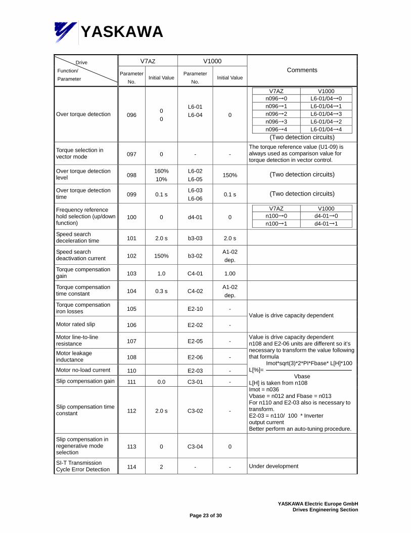
Over torque detection 096 0 0
L6-01 L6-04
0
V7AZ V1000 n096→0 L6-01/04→0 n096→1 L6-01/04→1 n096→2 L6-01/04→3 n096→3 L6-01/04→2 n096→4 L6-01/04→4
(Two detection circuits)
Torque selection in vector mode 097 0 - -
The torque reference value (U1-09) is always used as comparison value for torque detection in vector control.
Over torque detection level 098
160% 10%
L6-02 L6-05
150% (Two detection circuits)
Over torque detection time 099 0.1 s
L6-03 L6-06
0.1 s (Two detection circuits)
Frequency reference hold selection (up/down function)
100 0 d4-01 0 V7AZ V1000
n100→0 d4-01→0 n100→1 d4-01→1
Speed search deceleration time 101 2.0 s b3-03 2.0 s
Speed search deactivation current 102 150% b3-02
A1-02 dep.
Torque compensation gain 103 1.0 C4-01 1.00
Torque compensation time constant 104 0.3 s C4-02
A1-02 dep.
Torque compensation iron losses 105 E2-10 -
Motor rated slip 106 E2-02 -
Value is drive capacity dependent
Motor line-to-line resistance 107 E2-05 -
Motor leakage inductance 108 E2-06 -
Motor no-load current 110 E2-03 -
Slip compensation gain 111 0.0 C3-01 -
Slip compensation time constant 112 2.0 s C3-02 -
Value is drive capacity dependent n108 and E2-06 units are different so it’s necessary to transform the value following that formula Imot*sqrt(3)*2*PI*Fbase* L[H]*100 L[%]= Vbase L[H] is taken from n108 Imot = n036 Vbase = n012 and Fbase = n013 For n110 and E2-03 also is necessary to transform. E2-03 = n110/ 100 * Inverter output current Better perform an auto-tuning procedure.
Slip compensation in regenerative mode selection
113 0 C3-04 0
SI-T Transmission Cycle Error Detection 114 2 - - Under development
YASKAWA Electric Europe GmbH Drives Engineering Section
Page 24 of 30
YASKAWAV7AZ V1000 Drive
Function/ Parameter
Parameter No.
Initial Value Parameter
No. Initial Value
Comments
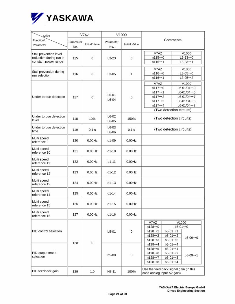
Stall prevention level reduction during run in constant power range
115 0 L3-23 0 V7AZ V1000
n115→0 L3-23→0 n115→1 L3-23→1
Stall prevention during run selection 116 0 L3-05 1
V7AZ V1000 n116→0 L3-05→0 n116→1 L3-05→2
Under torque detection 117 0 L6-01 L6-04
0
V7AZ V1000 n117→0 L6-01/04→0 n117→1 L6-01/04→5 n117→2 L6-01/04→7 n117→3 L6-01/04→6 n117→4 L6-01/04→8
(Two detection circuits)
Under torque detection level 118 10%
L6-02 L6-05
150% (Two detection circuits)
Under torque detection time 119 0.1 s
L6-03 L6-06
0.1 s (Two detection circuits)
Multi speed reference 9 120 0.00Hz d1-09 0.00Hz
Multi speed reference 10 121 0.00Hz d1-10 0.00Hz
Multi speed reference 11 122 0.00Hz d1-11 0.00Hz
Multi speed reference 12 123 0.00Hz d1-12 0.00Hz
Multi speed reference 13 124 0.00Hz d1-13 0.00Hz
Multi speed reference 14 125 0.00Hz d1-14 0.00Hz
Multi speed reference 15 126 0.00Hz d1-15 0.00Hz
Multi speed reference 16 127 0.00Hz d1-16 0.00Hz
PID control selection b5-01 0
PID output mode selection
128 0
b5-09 0
V7AZ V1000 n128→0 b5-01→0 n128→1 b5-01→1 n128→2 b5-01→2 n128→3 b5-01→3 n128→4 b5-01→4
b5-09→0
n128→5 b5-01→1 n128→6 b5-01→2 n128→7 b5-01→3 n128→8 b5-01→4
b5-09→1
PID feedback gain 129 1.0 H3-11 100% Use the feed back signal gain (in this case analog input A2 gain)
YASKAWA Electric Europe GmbH Drives Engineering Section
Page 25 of 30
YASKAWAV7AZ V1000 Drive
Function/ Parameter
Parameter No.
Initial Value Parameter
No. Initial Value
Comments
PID proportional gain (P) 130 1.0 b5-02 1.00
PID integral time (I) 131 1.0 s b5-03 1.0 s
PID derivative time (D) 132 0.0 s b5-05 0.00 s
PID output offset 133 0.0% b5-07 0.0%
PID integral limit 134 100% b5-04 100%
PID output delay time 135 0.0 s b5-08 0.00 s
PID feedback loss detection 136 0 b5-12 0
V7AZ V1000 n136→0 b5-12→0 n136→1 b5-12→1 n136→2 b5-12→2
PID feedback loss detection level 137 0% b5-13 0%
PID feedback loss detection time 138 1.0 s b5-14 1.0 s
Auto tuning selection 139 0 T1-01 0
V7AZ V1000 n139→0 n139→1 T1-01→0 n139→2 T1-01→2
Motor 2 maximum output frequency 140 50.0 Hz E3-04 50.0 Hz
Default setting in V1000 depends on control mode and o2-09 setting range by drive capacity and V/f pattern selection
PTC thermistor input motor overheat protection selection
141 0 L1-03 L1-04
3 1
V7AZ V1000 n141→0 - n141→1
n141→2,5 L1-04→ 0 n141→3,6 L1-04→ 2
n022→C1-09 n141→4,7
L1-03→3
L1-04→ 1
Motor temperature input filter time constant 142 0.2 sec L1-05 0.2 sec
Sequence input redundant reading selection Stop position control selection
143 0 - -
n143 = 1 Function is not necessary due faster scan cycle on V1000 n143 = 2 (Simple positioning control) will be implemented in the future
Stop position control compensation gain 144 1.00 - - Function not necessary in V1000
Bi-directional function selection 145 0 - -
Application dependant. Please contact supplier
Frequency offset selection 146 0 - -
n146=0x d3-01=n083…. n146=1x d7-01=+/-n083 * 100 / fmax n146=2x d7-01=+/-n083
Motor 2 maximum voltage output frequency
147 50.0 Hz E3-06 50.0 Hz
Pulse input scaling 149 2500 Hz H6-02 1440Hz
YASKAWA Electric Europe GmbH Drives Engineering Section
Page 26 of 30
YASKAWAV7AZ V1000 Drive
Function/ Parameter
Parameter No.
Initial Value Parameter
No. Initial Value
Comments
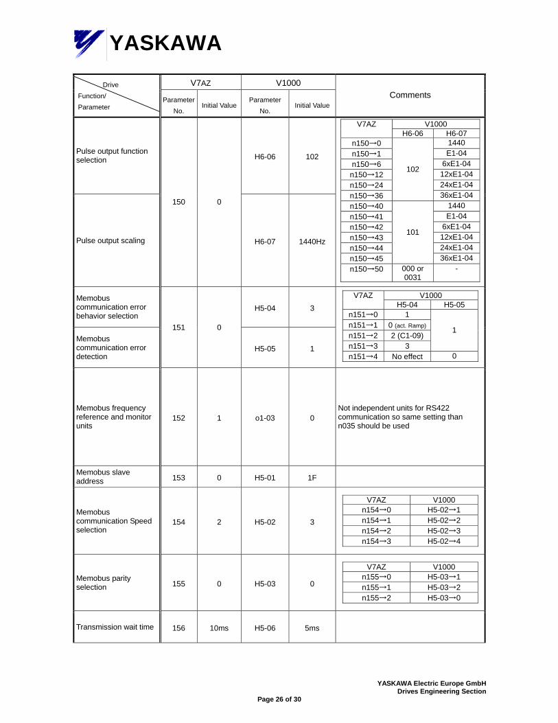
Pulse output function selection H6-06 102
Pulse output scaling
150 0
H6-07 1440Hz
V1000 V7AZ H6-06 H6-07
n150→0 1440 n150→1 E1-04 n150→6 6xE1-04 n150→12 12xE1-04 n150→24 24xE1-04 n150→36
102
36xE1-04 n150→40 1440 n150→41 E1-04 n150→42 6xE1-04 n150→43 12xE1-04 n150→44 24xE1-04 n150→45
101
36xE1-04 n150→50 000 or
0031 -
Memobus communication error behavior selection
H5-04 3
Memobus communication error detection
151 0
H5-05 1
V1000 V7AZ H5-04 H5-05
n151→0 1 n151→1 0 (act. Ramp) n151→2 2 (C1-09) n151→3 3
1
n151→4 No effect 0
Memobus frequency reference and monitor units
152 1 o1-03 0 Not independent units for RS422 communication so same setting than n035 should be used
Memobus slave address 153 0 H5-01 1F
Memobus communication Speed selection
154 2 H5-02 3
V7AZ V1000 n154→0 H5-02→1 n154→1 H5-02→2 n154→2 H5-02→3 n154→3 H5-02→4
Memobus parity selection 155 0 H5-03 0
V7AZ V1000 n155→0 H5-03→1 n155→1 H5-03→2 n155→2 H5-03→0
Transmission wait time 156 10ms H5-06 5ms
YASKAWA Electric Europe GmbH Drives Engineering Section
Page 27 of 30
YASKAWAV7AZ V1000 Drive
Function/ Parameter
Parameter No.
Initial Value Parameter
No. Initial Value
Comments
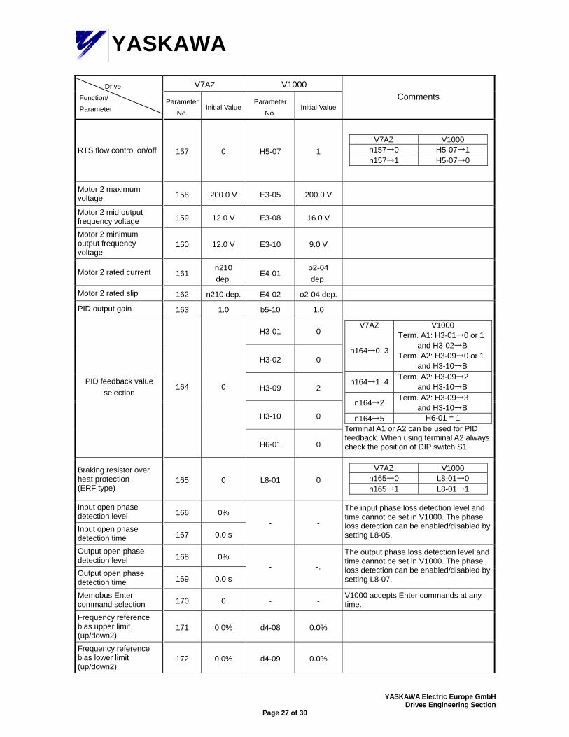
RTS flow control on/off 157 0 H5-07 1 V7AZ V1000
n157→0 H5-07→1 n157→1 H5-07→0
Motor 2 maximum voltage 158 200.0 V E3-05 200.0 V
Motor 2 mid output frequency voltage 159 12.0 V E3-08 16.0 V
Motor 2 minimum output frequency voltage
160 12.0 V E3-10 9.0 V
Motor 2 rated current 161 n210 dep.
E4-01 o2-04 dep.
Motor 2 rated slip 162 n210 dep. E4-02 o2-04 dep.
PID output gain 163 1.0 b5-10 1.0
H3-01 0
H3-02 0
H3-09 2
H3-10 0
PID feedback value selection
164 0
H6-01 0
V7AZ V1000
n164→0, 3
Term. A1: H3-01→0 or 1 and H3-02→B Term. A2: H3-09→0 or 1 and H3-10→B
n164→1, 4 Term. A2: H3-09→2 and H3-10→B
n164→2 Term. A2: H3-09→3 and H3-10→B
n164→5 H6-01 = 1 Terminal A1 or A2 can be used for PID feedback. When using terminal A2 always check the position of DIP switch S1!
Braking resistor over heat protection (ERF type)
165 0 L8-01 0 V7AZ V1000
n165→0 L8-01→0 n165→1 L8-01→1
Input open phase detection level 166 0%
Input open phase detection time 167 0.0 s
- -
The input phase loss detection level and time cannot be set in V1000. The phase loss detection can be enabled/disabled by setting L8-05.
Output open phase detection level 168 0%
Output open phase detection time 169 0.0 s
- -.
The output phase loss detection level and time cannot be set in V1000. The phase loss detection can be enabled/disabled by setting L8-07.
Memobus Enter command selection 170 0 - -
V1000 accepts Enter commands at any time.
Frequency reference bias upper limit (up/down2)
171 0.0% d4-08 0.0%
Frequency reference bias lower limit (up/down2)
172 0.0% d4-09 0.0%
YASKAWA Electric Europe GmbH Drives Engineering Section
Page 28 of 30
YASKAWAV7AZ V1000 Drive
Function/ Parameter
Parameter No.
Initial Value Parameter
No. Initial Value
Comments
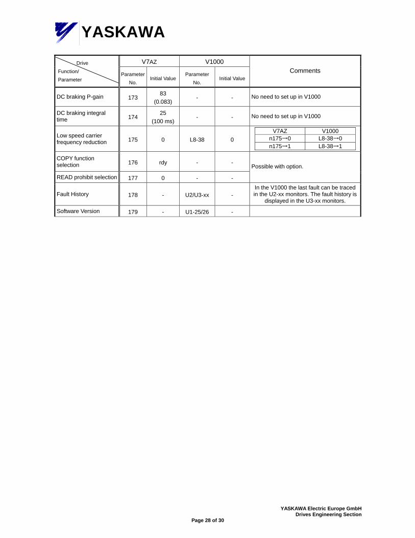
DC braking P-gain 173 83
(0.083) - - No need to set up in V1000
DC braking integral time 174
25 (100 ms)
- - No need to set up in V1000
Low speed carrier frequency reduction 175 0 L8-38 0
V7AZ V1000 n175→0 L8-38→0 n175→1 L8-38→1
COPY function selection 176 rdy - -
READ prohibit selection 177 0 - -
Possible with option.
Fault History 178 - U2/U3-xx - In the V1000 the last fault can be traced in the U2-xx monitors. The fault history is
displayed in the U3-xx monitors.
Software Version 179 - U1-25/26 -
YASKAWA Electric Europe GmbH Drives Engineering Section
Page 29 of 30
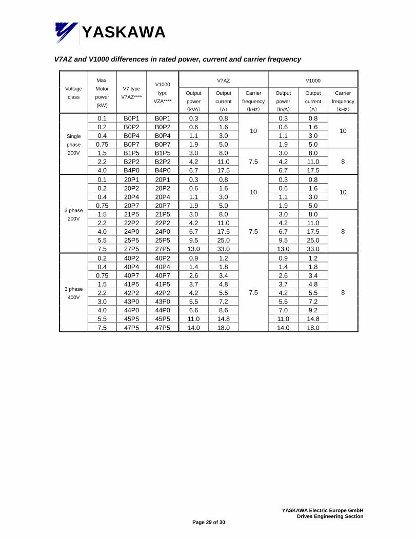
YASKAWAV7AZ and V1000 differences in rated power, current and carrier frequency
V7AZ V1000 Voltage class
Max. Motor power (kW)
V7 type V7AZ****
V1000 type
VZA**** Output power
(kVA)
Output current (A)
Carrier frequency(kHz)
Output power
(kVA)
Output current (A)
Carrier frequency(kHz)
0.1 B0P1 B0P1 0.3 0.8 0.3 0.8 0.2 B0P2 B0P2 0.6 1.6 0.6 1.6 0.4 B0P4 B0P4 1.1 3.0 1.1 3.0 0.75 B0P7 B0P7 1.9 5.0
10
1.9 5.0
10
1.5 B1P5 B1P5 3.0 8.0 3.0 8.0 2.2 B2P2 B2P2 4.2 11.0 4.2 11.0
Single phase 200V
4.0 B4P0 B4P0 6.7 17.5 7.5
6.7 17.5 8
0.1 20P1 20P1 0.3 0.8 0.3 0.8 0.2 20P2 20P2 0.6 1.6 0.6 1.6 0.4 20P4 20P4 1.1 3.0 1.1 3.0 0.75 20P7 20P7 1.9 5.0
10
1.9 5.0
10
1.5 21P5 21P5 3.0 8.0 3.0 8.0 2.2 22P2 22P2 4.2 11.0 4.2 11.0 4.0 24P0 24P0 6.7 17.5 6.7 17.5 5.5 25P5 25P5 9.5 25.0 9.5 25.0
3 phase 200V
7.5 27P5 27P5 13.0 33.0
7.5
13.0 33.0
8
0.2 40P2 40P2 0.9 1.2 0.9 1.2 0.4 40P4 40P4 1.4 1.8 1.4 1.8 0.75 40P7 40P7 2.6 3.4 2.6 3.4 1.5 41P5 41P5 3.7 4.8 3.7 4.8 2.2 42P2 42P2 4.2 5.5 4.2 5.5 3.0 43P0 43P0 5.5 7.2 5.5 7.2 4.0 44P0 44P0 6.6 8.6 7.0 9.2 5.5 45P5 45P5 11.0 14.8 11.0 14.8
3 phase 400V
7.5 47P5 47P5 14.0 18.0
7.5
14.0 18.0
8
YASKAWA Electric Europe GmbH Drives Engineering Section
Page 30 of 30
YASKAWARevision History
Rev. No. Date Modification
- 31. March 2007 First Edition