Recorder and Player User's Guide - Conferencing | Web Conferencing
Upload
satyanpitrodaCategory
view
28download
0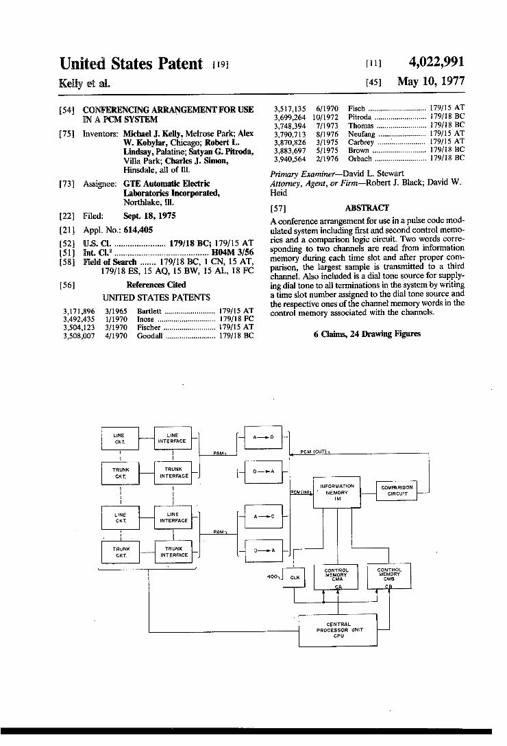
0 “H 1% Unit States Patent [191 [111 4,022,991 Key et .. [45] , May 10, 1977
[54] CUNFERENCING ARRANGEMENT FOR USE 3,517,135 6/1970 Fisch ........................... .. 179/15 AT TN A PCM SYSTEM 3,699,264 10/1972 Pitroda . . . . . . . . . .. 179/ 18 BC
. 3,748,394 7/1973 Thomas . . . . . . . . .. 179/18 BC
[751 Inventors: Michael J- Kelly2 Melrose Park;A1eX 3,790,713 8/1976 Neufang 179/15 AT W. Kobylar, Chicago; Robert L. 3,870,826 3/1975 Carbrey 179/15 AT Lindsay, Palatine; Satyan G. Pitroda, 3,883,697 5/1975 Brown ................. .. 179/18 BC Villa Park; Charles J, Simon, 3,940,564 2/1976 Orbach ........................ .. 179/18 BC
_ Hmsdale’ a“ of “1' Primary Examiner-—David L. Stewart [73] Assignee: GTE Automatic Electric Attorney, Agent, or Firm-Robert J. Black; David W.
Laboratories Incorporated, Heid Northlake, Ill. 57 ABS CT
[22] Filed: Sept. 18, 1975 [ 1 . A conference arrangement for use m a pulse code mod
[21] APPI- N04 614,405 ulated system including ?rst and second control memo [52] us. Cl. ..................... .. 179/18 R0 179/15 AT ?es and a comparison logic circuit TWO Words “me [51] int. C1.2 ........................................ ..’H04M 3/56 Sponding to two chant/e18 are read from information [58] Field of Search ..... .. 179/18 BC, 1 CN, 15 AT, memory durmg each "me $19‘ and after Proper c0?“
179/18 ES, 15 A0, 15 Bw 15 AL 18 FC parison, the largest sample is transmitted to a thlrd _ ’ ’ channel. Also included is a dial tone source for supply
[56] References Clted ing dial tone to all terminations in the system by writing UNITED STATES PATENTS a time slot number assigned to the dial tone source and
‘ the respective ones of the channel memory words in the 3,171,896 3/1965 Bartlett ....................... .. 179/15 AT ' ' 3,492,435 1/1970 [nose .................... .. 179/18 FC control memory assoclated “nth the channels‘
3,504,123 3/1970 Fischer . . . . . . . . .. 179/15 AT
3,508,007 4/1970 Goodall ....................... .. 179/ 18 BC 6 Claims, 24 Drawing Figures
INT: 135m '_ A“ D
: { PAM (PCM (OUTlu
T218?‘ —' millage: _ — D—’A 7'
i i M ~ '~ mm?" 1 I IM
7"“ lNTLElggAcE 7' _ ‘in-'0 T
: l PAM | > 1
T35?“ ‘NT/£21K“ ~ — Pr“ — '—\
CMA CMB
A CB
CENTRAL PROCESSOR UNIT
CPU


US“ Patent May 10, 1977 Sheet4 of 17 4,022,991
A-I, B-I, C-l TO FIG 5
T0 GATES 6008-900
T0 GATES H00
03C. 6.!76 MHz
CLOCK 400
FRAME RESET
QA
QB
EARLY COUNTER _l 403

US. Patent
FRO CLOCK 400
FIG. 4
l_______l
May 10, 1977 Sheet 5 of 17 4,022,991
DRIVERS 560
CHANNEL SHIFT REG.
CONTROL LOGIC 550
STROBE PULSE GENERATOR 500
5071.
PRESET-l


U03w Patent May 10, 1977 Sheet 7 of 17 4,022,991
INFORMATION MEMORY (96x8)
R/W l MEMORY
R/W 6 MEMORY
R/W 7 MEMORY
I I | | |
PW ‘T
I | | l I


US, Patent May 10, 1977 Sheet 9 of 17 4,022,991
FROM TIME @; 903 8,64 SLOT COUNTER c4: ‘):———————
402 ‘
- 1sELEcT
’s|-o3 AO-O\ A'o
S2-O‘\ 1*‘
A|-O\ A-21
c|-o\ A
A2-O\ 3 FROM
cz-o ,
TIME SLOT \ STEERING COUNTER A3‘ow GATE 4 2 o C4-O\
A4-O\ CEI]
ca-ow c523
A5701 cs3]
GIG-0w DECIMAL C54 \ A6_O DECODER ____1
K900 C551 FROM CPU .¢E.__61
LOW ADDRESS STORAGE
I220 ‘
_ L\90!
R/W CA(A+B)-Ow
FROM FIG. I3
R/W CB(A+B)-O\
r DH) \
0243
03-h -
FROM CPU -Pi!l—-> DATA STORAGE ’
|2|o _D_5i___,:
D64)
Q74) _
DB-I \
FIG. 9


atent May 10, 1977 Sheet 11 of 17 4,022,991
N: 20mm
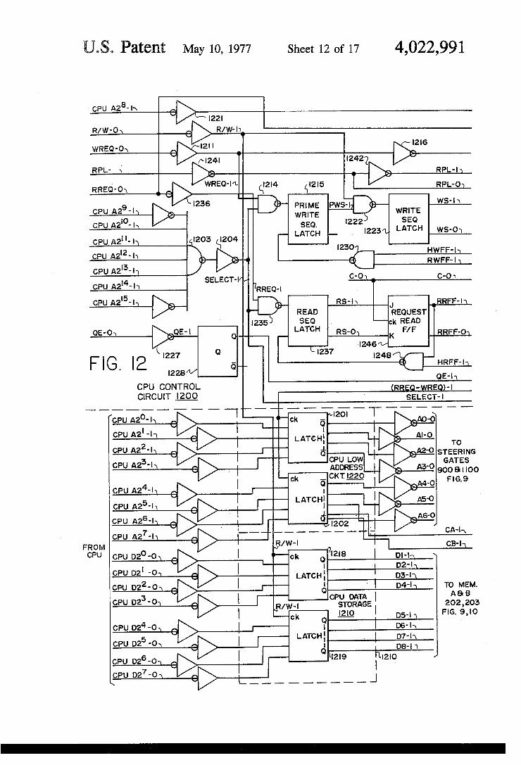
May 10, 1977 Sheet 12 of 17 4,022,991
I203 I204
SELECT
J REQUEST READ F/F
'2 I227 I228
CPU CONTROL CIRCUIT I200
CPU DATA | STORAGE me I

HE“ Patent May 10, 1977 Sheet 13 of 17 4,022,991
CH-l MEMORY SELECT
F/F CA OR
I324 I325 CB-l
J REQUEST WRITE F/F
WRITE STROBE DRIVES CKT.
I309
J HAVE
WRITTEN
K K
QE HWFF-l
READY 88-!
FIG. I?)
STEERING GATE & LATCH
FROM CHANNEL MEMORY
CH DATA CKT. CPU lREAD BACK! I300 BUFFERS

U0. Patent May 10, 1977 Sheet 14 of 17 4,022,991
TRANSMIT AME TRANSMIT TRANSMIT T FILTER GATE
TO
V _/_ TRANSMIT PAM BUS:
-50 / I402 11404 L 5» I403 TRANSMIT ENABLE EN-I w
A RECEIVE AMF.‘ RECEIVE ll FILTER RECEIVE GATE
FROM
U / RECEIVE PAM Busw I
= |4o7 k 11405 R I406 {RECEIVE ENABLE (EN-I);
LINE CIRCUIT
I5OI FROM CHE STROBE FIG.5 CHE (x) sB-o
I f I502 [I503 CHE 1-01 TRANSMIT ENABLE; I
cHE2-o1 I TRANSMIT I (EN-IV CHE4-O1 I GATE : CHE8-O I ENABLE
FROM CHEM; TRANSMIT | DECODES I FIG. I I '\ BUFFER l (FUNCTION I
CHE3Z'Ow I OF I CHE64-O1 I TgDEUSLg I LcHEmB-m I 402) TRANSMIT ENABLE
(EN-NV
[I505 [I506 RECEIVE ENABLE
"’ - ' (EN-n/
-> RGEcEIE/E ' i > AT I
_‘ SH'FT ENABLE I ‘ : REGISTER DECODES I
:(DELAY OF (FuNézFrloN : =7 CHANNELS TIME SLOT I E COUNTER I -; 4°31 w.
(EN-NV
w
FIG. I5


4,022,991 1
CONFERENCING ARRANGEMENT FOR USE IN A PCM SYSTEM
BACKGROUND OF THE INVENTION
1. Field of the Invention This invention relates generally to switching and
transmission techniques in telephone communication systems, and more particularly to an improved switch ing technique for connecting several pulse code modu lated channels in a typical PCM system for conferenc ing. More particularly still, the invention relates to an improved switching and transmission technique for use in such a PCM system for reducing the common equip ment required for a speci?ed number of terminations, using a method and arrangement of channel allocation as compared to the usual dedicated channel arrange ment.
2. Description of the Prior Art In general, in most prior art systems wherein analog
conference circuits are provided, the analog signals of all participants are compared and then all signals to an individual participant with the exception of the signals generated by that individual himself are extended. A variety of schemes such as direct multiplexing, hybrid repeaters, transistorized analog circuitry, etc. have been utilized. Various solutions to the problems of cross talk, echo loss, impedance matching, sidetone, etc. have been disclosed. Some of the techniques em ployed are shown in US. Pat. Nos. 3,116,369; 3,144,518; 3,170,042 and 3,301,962. None of the tech niques disclosed employ the digital approach and hence are of little signi?cance in the ?eld of pulse code modulated telephony. A conference circuit for a time division multiplex telephone communication system is disclosed in US. Pat. No. 3,551,600. In this disclosure, digital techniques are employed. However, the time division signals are still in analog form and after being acted upon by the conference circuit, they must be reconverted from digital to analog form.
In US. Pat. No. 3,699,264, there is disclosed an algorithm for providing digital pulse code modulated conferences. In the disclosed system, during every time frame, an active speaker sample is sought. The active speaker is identi?ed by comparing each participant’s digital sample during the following time frame. The active speaker sample is transmitted to all participants in the conferencing arrangement. A last speaker sam ple is transmitted to the active speaker. With this ap proach, a three-way conferencing per circuit is possible in its digital form. While the arrangement disclosed in this US. Pat. No.
3,699,264 has found application in various systems, in existing commercial PABX systems having a large number of trunks, a very large number of three-way conferencing circuits would be required. Accordingly, it would be desirable to provide in such systems, a three-way conferencing facility through the switching network. As indicated above, one aspect of the present invention relates to such a switching technique for connecting several pulse code modulated channels for conferencing.
Presently known all-time pulse code modulated sys tems generally are arranged with the transmit side of each inlet appearing in a fixed position on one side of the switching network, and with the receive side of each inlet appearing in a ?xed position on the other side thereof. The operation is such that all information
20
25
35
45
50
55
60
65
2 entering from the input pulse code modulated (PCM) bus is stored and made available at the output under the control of a control memory which contains infor mation regarding all network connections. More particularly, in such systems, in a normal oper
ation, each channel arriving on the input bus is written cyclically into a ?xed location in an information mem ory. At this time, the control memory word corre sponding to that channel is read for addressing the information memory. The content of the information memory at this address (which represents a PCM sam ple from the channel engaged in a conversation with the other channel) is read out. The same operation of writing the information memory, reading the control memory for the information memory address, and reading the information memory is performed during the other channels time slot. In any given channel loca tion, the control memory contains the address of the channel to which it is to be connected. Such all-time PCM systems do not have the ability to provide a dou ble connection for conferencing.
SUMMARY OF THE INVENTION
In accordance with the present invention, conferenc ing can be provided in such a PCM system by providing two additional circuits, namely, a second control mem ory and a comparison logic circuit. With the addition of these two circuits, the operation is such that two words corresponding to two channels are read from the infor mation memory every time slot, and after proper com parison, the largest sample is transmitted to the third channel. In other words, assuming, for example, that channels 3, 5 and 9 are engaged in a three-way confer ence, during the channel 3 time slot, the samples from channel 5 and channel 9 are read and compared, and the larger of the two samples is transmitted to channel 3. Subsequently, during the channel 5 time slot, the samples from channel 3 and channel 9 are read and compared, and the larger of the two samples is trans mitted. During the channel 9 time slot, the operation is repeated, with the largest of the channel 3 and 5 sam ples being transmitted. It can be seen that during each channel time slot, the incoming information is written into the ?xed channel number in the information mem ory and the outgoing information is read from some other channel speci?ed in the control memory. This operation of writing and reading the information mem ory goes on continuously during each channel. The next time frame, new PCM samples are written into the information memory. With this arrangement and technique, several advan
tages result, including the fact that it provides three way calling facility with a minimum of hardware and provides three-way calling ability per port. Also, since the four-wire PCM network has the ability to switch transmit and receive ports separately, three-way calling in any desired direction is possible. In other words, it is possible to provide a call waiting tone to just one of the subscribers in a normal conversation. The same ability is also provided for consultation. The comparison and other signal processing is performed on line. Maximum advantage is taken of the existing information memory and other addressing circuits, and only one additional control memory and comparison logic is required to perform the conferencing function. The addition of three-way calling ability does not disturb normal net work connection, and the arrangement furthermore is expandable along with the network. In view of the

4,022,99 :1 3
centralized three-way calling ability, a single source such as a call waiting tone can be connected for all possible double connections. The system is all digital, using only digital circuits, and further can be used with the D2 encoding format with logarithmic characteris tics. Since it is digital, the problems related to loading, impedance matching, etc. are irrelevant. The above generally described PCM system provides
non-blocking switching, with a channel per each termi nal equipment being provided. In other words, it is a dedicated channel arrangement. In many applications such as, for example, with a small EPABX where less than 10 cos of traffic is common, an improvement in the switching concept can be provided in the form of smaller system costs and size (physical) at the same transmission levels but at the expense of ?exibility. The reduction in ?exibility is a result of making the system blocking to an extent, however, in systems such as a small EPABX, no real ?exibility is lost since-no real requirement for anon-blocking system exists.
In accordance with the present invention, such a system can be provided by using a method and arrange ment which is a condensation of the required channels provided to time division switching by distribution of the channels instead of the usual dedicated channel method. In this system, a channel memory is created and provided to provide for control of which terminal equipments are allotted which channels (on a'per call basis). In the hereinafter disclosed system, the channel memory has 96 locations and each location stores the associated equipment which has been allocated that channel. The control of the channel memory (data update) is performed by a call processor unit (CPU) when connections are established or removed. The memory, however, also constantly is cyclically read and the associated equipment is given a channel transmit and receive pulse as long as its identity is storedin the memory. The distribution of these pulses is actually a decode of the memoryread out, with the latter being stored external to the memory for a speci?ed time. Each equipment decodes this data to see if it corre sponds to its identity. If it does, that equipment is en abled as long as the storage contains its identity. _ Accordingly, it is an object of the present invention
to provide an improved switching technique for con necting several pulse code modulated channels in a typical PCM system for conferencing. , More particularly, another object is to provide an
improved switching and transmission technique for use in such a PCM system for reducing the common equip ment required for a speci?ed number of terminations using a method and arrangement of channel allocation.
BRIEF DESCRIPTION OF THE DRAWINGS
FIG. 1 is a block diagram schematic of a telephone communication system employing an ‘improved switch ing technique for connecting several pulse code modu lated channels in a typical PCM systemfor conferenc ing, in accordance with a'?rst embodiment of the in vention; ,
FIGS. 2 and 3 are block diagram schematic and an expanded block diagram schematic, respectively, of a PCM system employing an improved switching and transmission technique exemplary of a second embodi ment of the invention, for reducing the common equip ment required for a specified number of terminations, by using a method and arrangement of channel alloca
15
25
35
45
50
-55
60
65
4 tion as compared to the usual dedicated channel ar rangement; FIG. 4 illustrates the clock used in the system of
FIGS. 2 and 3; FIG. 5' illustrates the control logic and the strobe
pulse generator of the system of FIGS. 2 and 3; FIGS. 6, 7_ and 8, when assembled as illustrated in
FIG. 20 illustrate the information memory, the steering gate for accessing it, the speaker latches at its output, the. comparator and the force null logic for receiving and sending PCM to the peripheral equipment, of the system of FIGS. 2 and 3; FIGS. 9 and 10, when assembled as illustrated in FIG.
21, illustrate the control memories, the steering gate for accessing them, and the steering gate for outputting data from the respective ones of the control memories, of the system of FIGS. 2 and 3; FIG. 11 illustrates the channel memory, the steering
gate for accessing it, and the channel identity latches at its output, of the system of FIGS. 2 and 3; FIGS. 12 and 13, when assembled as shown in FIG.
22, illustrate the CPU control circuit, the CPU low address circuit, the CPU data storage circuit, and CPU data read back circuit, of the system of FIGS. 2 and 3; FIG. 14 illustrates a typical line circuit in the system
of FIGS. 2 and 3; 7 FIG. 15 illustrates a typical line termination in the system of FIGS. 2 and 3; FIGS. 16 A-l6C and 17 are pulse timing charts illus
trating various clock and timing pulses of the system of FIGS. 2 and 3; FIGS. 18 and 19 illustrate the manner in which the
channel memory and the control memories are viewed as one large memory for accessing, in the system of FIGS. 2 and 3; and FIGS. 20-22 illustrate how the various indicated
?gures are assembled.
GENERAL DESCRIPTION
Referring now to the drawings, in FIG. 1 there is illustrated a stored program digital PCM-EPABX sys tem which can be divided into four main blocks, namely, a PCM interface, a PCM network, a number of miscellaneous circuits, and a control complex. The PCM interface consists of the line and trunk interfaces, the analog to digital (A/D) and digital to analog (D/A) converters and their associated multiplexers, and pro vides analog to PCM and PCM to analog conversions and the necessary time division multiplexing. The all time non-blocking PCM network, with full availability, consists of an information memory, a clock, two con trol memories and a comparison circuit, and switches (in time) the coded information received from the PCM interface. The miscellaneous circuits, for pur poses of clarity are not shown, but include all of the required service circuits, such as tone generators, tone receivers, conference circuits and circuitry for turret control. The control complex consists of the micro processor or central, processor unit (CPU) and the instruction and process stores. The CPU has direct ‘access to the lines, trucks and miscellaneous circuits for scanning and control; and to the PCM network for establishing the connections. Theanalog information from a subscriber is ampli
fled, and sampled (at 8 KHZ) at the line interface. The sampled information from 24 line and trunk interface circuits is combined together to form a 24 channel PAM (pulse amplitude modulated) bus. An analog to