University of California at Berkeleycs150/fa07/Labs/Checkpoint1.doc · Web viewUniversity of...
18
EECS150 Fall 2007 Checkpoint1 UNIVERSITY OF CALIFORNIA AT BERKELEY COLLEGE OF ENGINEERING DEPARTMENT OF ELECTRICAL ENGINEERING AND COMPUTER SCIENCE Checkpoint 1 AC97 Audio 1.0 Motivation One of the most difficult aspects of digital design is interfacing with a circuit or IC designed by someone else, however it is also the most important part. For this reason, a major part of the EECS150 project is interfacing your circuits both to those designed by your partner, who you can work with on debugging, and to those designed by professionals with whom you cannot interact, save through their documentation (a good reason to take E190 seriously). In this checkpoint, for the first time we are asking you to read a datasheet, a complete specification of the operation of an integrated circuit: in this case the LM4549A AC97 audio codec. Armed with this specification, you will proceed to build a controller to initialize and then provide PCM audio data to that chip. The specification can be downloaded from http://www-inst.eecs.berkeley.edu/~cs150/Documents/LM4549A.p df . It will be especially useful to look at pages 15-24 in the specification document. At the end of the checkpoint, you should be able to record and playback audio by using the push buttons on the FPGA and use the dipswitches to toggle the volume levels. 2.0 Introduction One of the primary reasons for building the CaLinx boards was the availability of such interesting audio and video I/O chips as the LM4549A AC97 Audio Codec you will be UCB 1 2007
Transcript of University of California at Berkeleycs150/fa07/Labs/Checkpoint1.doc · Web viewUniversity of...
EECS150 Fall 2007 Checkpoint1
UNIVERSITY OF CALIFORNIA AT BERKELEYCOLLEGE OF ENGINEERING
DEPARTMENT OF ELECTRICAL ENGINEERING AND COMPUTER SCIENCE
Checkpoint 1AC97 Audio
1.0 MotivationOne of the most difficult aspects of digital design is interfacing with a circuit or
IC designed by someone else, however it is also the most important part. For this reason, a major part of the EECS150 project is interfacing your circuits both to those designed by your partner, who you can work with on debugging, and to those designed by professionals with whom you cannot interact, save through their documentation (a good reason to take E190 seriously).
In this checkpoint, for the first time we are asking you to read a datasheet, a complete specification of the operation of an integrated circuit: in this case the LM4549A AC97 audio codec. Armed with this specification, you will proceed to build a controller to initialize and then provide PCM audio data to that chip. The specification can be downloaded from http://www-inst.eecs.berkeley.edu/~cs150/Documents/LM4549A.pdf. It will be especially useful to look at pages 15-24 in the specification document.
At the end of the checkpoint, you should be able to record and playback audio by using the push buttons on the FPGA and use the dipswitches to toggle the volume levels.
2.0 IntroductionOne of the primary reasons for building the CaLinx boards was the availability of
such interesting audio and video I/O chips as the LM4549A AC97 Audio Codec you will be controlling in this checkpoint. This codec, and others like it, have been used in computers for years.
The FPGA and the LM4549A are connected by a relatively simple digital interface consisting of a 12.288MHz clock generated by the Codec, two bit serial data lines and a sync signal to synchronize the data between the FPGA and Codec.
For the first part of this checkpoint your primary goal is to work on generating the AP_RESET_, AP_SYNC and AP_SDATA_OUT signals which go to the Codec. For more information about these signals, see the section 2.3 AC97 Interface Spec below.
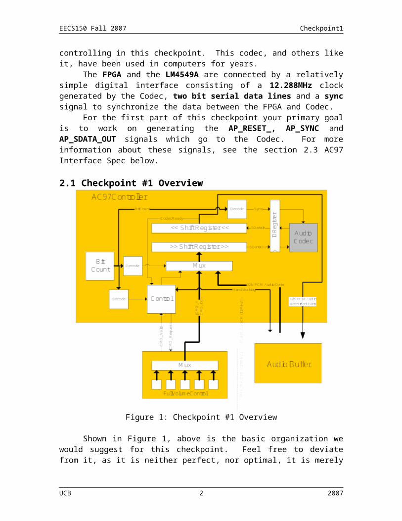
2.1 Checkpoint #1 Overview
UCB 1 2007
EECS150 Fall 2007 Checkpoint1
Figure 1: Checkpoint #1 Overview
Shown in Figure 1, above is the basic organization we would suggest for this checkpoint. Feel free to deviate from it, as it is neither perfect, nor optimal, it is merely a vague idea to get you started thinking for your design review.
At the core, the AC97 controller is effectively a parallel to serial converter designed to convert the 32b PCM samples into 256b AC97 frames. Its other duties include generating the proper synchronization and reset signals required for correct operation of the LM4549A.
Please note the IORegister module shown in the above diagram. This module will act like a standard register in that it will delay all of your signals between the LM4549A and your AC97Controller. However if you look inside the module you will see the text // synthesis syn_useioff = 1, which will cause the synthesis and PAR tools to place that register at the very edge of the FPGA just as the signals leave and enter the chip. This register is required for timing reasons, without it your design will work only occasionally and only on certain CaLinx2 boards.
2.2 AC97 Audio CodecThe AC97 Audio Codec is simply a chip meant to convert between analog audio
signals such as those going to the speakers/microphone and digital PCM signals which are easy to work with on an FPGA or in a computer.
UCB 2 2007

EECS150 Fall 2007 Checkpoint1
If you are interested in any of this, take a look at the analog sections of the datasheet. In this lab we will focus on how to use the chip, not what it can do or how it works.
2.2.1 Block Diagram (Page 2 of the LM4549A Datasheet)Below is the block diagram of the audio paths in the codec. It shows the inputs,
outputs, volume controls and mixers. Notice that the signals should remind you of those on a common PC volume control; however we will not be using most of them. In fact many of the analog inputs are tied to ground on the CaLinx2 boards.
Figure 2: LM4549A Block Diagram
2.2.2 Register Map (Page 15, 22-24 of the LM4549A Datasheet)Most of programming the LM4549A consists of writing the control registers to
change volume settings and PCM audio rates. For this you will send register write commands using Slot1 and 2 in the output data stream. Slot1 will contain the address of the register to write and Slot2 will contain the data to write.
UCB 3 2007

EECS150 Fall 2007 Checkpoint1
Figure 3: Partial LM4549A Register Map
Notice that most of the registers in the register map will not be used. We will concentrate on the following registers:
Master Volume: The master volume control (affects the headphone jack) Line Level Volume: The line level volume control (affects the line out jacks) Line In Volume: The line level volume control (affects the line in jacks). PCM Out Volume: Digital audio output volume (affects audio from the FPGA) PCM Audio Rate: (DAC and ADC)Controls the rate of digital to analog
conversions (4kHz) Record Gain: Controls the mute and gain of the microphone recording Record Select: Controls which input will be used to record.
You do not and should not need to change the Mic Volume as changing this register will make the microphone analog input go straight out to line out jacks. We want to record the audio through the record gain register.
UCB 4 2007

EECS150 Fall 2007 Checkpoint1
2.3 AC97 Interface Spec
2.3.1 Reset and ClockingClocking and resetting the LM4549A AC97 codec is vital. Because the codec
generates the AP_BIT_CLOCK signal when AP_RESET_ (notice the trailing underscore indicating active low logic) is asserted, AP_BIT_CLOCK will stop oscillating.
As you may recall from lecture, you were admonished against the use of gated clocks because it causes exactly the kind of problems you will encounter when interacting with the AC97 codec: namely if you generate AP_RESET_ improperly, the circuit will lose its clock and lock up permanently.
For this reason, we have provided you with the LocalResetGen.v module as detailed in section below.
This module will use the 27MHz clock provided directly from a crystal on the board, to generate the 1us wide reset pulse required by AP_RESET_ signal. It will also generate a secondary reset, which you can use to reset your registers which depend on AP_BIT_CLOCK.
2.3.2 Sync (Frame Synchronization)In order to synchronize the serial data on the AP_SDATA_IN and
AP_SDATA_OUT lines, as well as let the Codec and FPGA know where they are in the bit stream, you AC97Controller.v must generate a synchronization signal: AP_SYNC.
This signal should be high for 16 cycles out of the 256 of each AC97 serial data frame. Note carefully which cycles. The codec must sample the sync signal high for each rising edge of the clock on which your AC97Controller transmits a bit from Slot0! This means that the sync signal should go high the cycle before you start sending a new frame. Or, in other words, on the same cycle as you assert the load signal to your output shift register to load the data for Slot0.
The LM4549A.v Verilog simulation model will check that you assert the AP_SYNC signal for the correct number of cycles (or more accurately it checks that you assert it for the correct length of time). However, the LM4549ACodec.v cannot check that you assert it at the right time; therefore if you assert the AP_SYNC signal at the wrong time, the LM4549ACodec will assume you got the AP_SYNC signal correct and will then complain about the serial data you are transmitting. The LM4549A will do the same. This is because the AP_SYNC signal is the only frame of reference these circuits have from which to decode the incoming bits.
2.3.3 Codec ReadyBecause the LM4549A is a complex mixed analog and digital chip, it actually
takes some time to power-on and to reset. As a result, you must wait for the chip to be ready before you can begin sending it commands or data. Fortunately waiting for this is very simple.
UCB 5 2007
EECS150 Fall 2007 Checkpoint1
To check if the LM4549A codec or the LM4549ACodec.v model is ready, simple capture the first bit of the data frame coming in over the SDataIn or AP_SDATA_IN line. When this bit (corresponding to bit15 of Slot0 of the incoming frame) is 1’b1, the codec is ready to receive commands and data.
If you attempt to send commands or data to the codec before this time, it may or may not work. The LM4549ACodec.v model will ignore all input before it asserts this signal and will not generate any valid output. The actual LM4549A may not be so well behaved.
2.3.4 Data Out (Page 17 of the LM4549A datasheet)The serial data output format is well documented in the LM4549A datasheet.
We suggest you read that thoroughly. Below is the timing diagram for an AC97 output frame.
Figure 4: AP_SDATA_OUT Timing
There are several important things to note about this diagram. The Audio Codec samples the AP_SDATA_OUT on the falling edge of
AP_BIT_CLOCK. This means that you should change the data on the rising edge.
o I.E. your output shift register should be positive edge triggered. The LM4549A will assume a frame is beginning on the first rising edge of
AP_BIT_CLOCK when it samples AP_SYNC as high. This means that AP_SYNC needs to go to 1’b1 one cycle before the start of a new frame.
o Failure to properly drive the sync (short for synchronize) signal will result in errors both in simulation with LM4549ACodec.V and on the board.
Remember that Slot0 (the tag slot) has only 16bits whereas the other 12 slots have 20bits each. (12*20 + 16 = 256b/frame)
Bits 10-0 of Slot0 should be set to 0 Remember to set the highest 5 bits of Slot0 properly. Do NOT send output frames until you have received a CodecReady signal.
UCB 6 2007

EECS150 Fall 2007 Checkpoint1
All of the contents of your output frames will be decoded and printed by LM4549ACodec.v, if your frames are properly formed
2.3.5 Data In (Page 19 of the LM4549A datasheet)The serial data input format is well documented in the LM4549A datasheet. We
suggest you read that thoroughly. Below is the timing diagram for an AC97 input frame.
Figure 5: AP_SDATA_IN Timing
There are several important things to note about this diagram You should sample AP_SDATA_IN on the rising edge of AP_BIT_CLOCK. The CodecReady bit should be moved into bit0 of the shift register on the second
rising edge where AP_SYNC is high. You MUST wait for CodecReady before attempting to use the audio codec.
2.3.6 Volume ControlsIf you examine the instantiation of FullVolumeControl.v in AudioTop.v, you will
find that there are a number of 6 wire inputs, each of which corresponds to a volume control shown in Figure 2, and outlined in section 2.2.2 Register Map (Page 15, 22-24 ofthe LM4549A Datasheet).
Your volume controls should be relatively simple. Currently in FPGA_TOP2, we have set the Speaker volume/mute and mic volume/mute signals to the SW9 and SW10 dipswitches. You should wire the speaker volumes to all of the outgoing volume levels and wire the mic volume to the incoming volume levels (i.e. the record gain register).
Most registers have 5bit volumes for left and right, plus a mute bit. Some have 4bit volumes! Keep an eye on the number of bits you are working with.
Some volumes are reversed in that higher numbers may mean quieter sounds. Make sure to check what the bits mean in the LM4549A Datasheet.
3.0 PrelabPlease make sure to complete the prelab before you attend your lab section. You
will not be able to finish this lab in 3hrs.
UCB 7 2007

EECS150 Fall 2007 Checkpoint1
1. Read this handout thoroughly. Pay particular attention to sections 2.0Introduction and 4.0 Lab Procedure.
2. Read the LM4549A Datasheeta. You can find this on the website: http://www-
inst.eecs.berkeley.edu/~cs150/Documents/LM4549A.pdf.3. Examine the Verilog provided for this weeks lab.
a. You should read and understand the AudioTop.v module.b. Feel free to change AudioTop.v. Ours is a starting point, not a
restriction.4. Take your design review seriously.
a. This week more than any other we are expecting you to design your own modules.
b. You will need your design review to get feedback on the things you did well, as well as the problems your design has.
c. Your design that you show in your design reviews should be detailed enough that you could give your design to another group and have them implement it from scratch.
d. You should have at least a block diagram for the entire module and every major module as well as any bubble and arc diagrams for any FSM that you have.
4.0 Lab ProcedureRemember to manage your Verilog, projects and folders well. Doing a poor
job of managing your files can cost you hours of rewriting code, if you accidentally delete your files.
Below are sections describing the various modules you may work with for this lab. Note that you will need at least one instance of each of these modules.
4.1 AudioTop.vThis module is complete from the standpoint that you do not HAVE to modify or
change it if you are capable of duplicating our solution to the checkpoint. However you should feel free to modify and extend this module.
You will have 32 bits of input and output for each audio sample. You will use 16 of these bits (either left channel or right channel) to store into the audio fifo as it is only 16 bits wide. When sending the data back into audiotop.v, you should duplicate the 16 bit wire, so that we have the same audio data for both the left channel and right channel audio (mono instead of stereo). We do this to conserve the number of bits we will eventually need to send through the wireless.
The audio_fifo will be able to hold roughly 8 seconds of audio using these 16 bit samples. When you press SW2, you should have the fifo begin to record the audio, and then play back the audio when you press SW3.
4.2 FullVolumeControl.vThis module should contain all of your volume control code. You may wish to
build a single standard volume control and instantiate it many times, or you may choose to write this module as a large piece of behavioral code, it is up to you.
UCB 8 2007

EECS150 Fall 2007 Checkpoint1
Signal Width
Dir
Description
SpeakerVolume 5 I Used to control the volume out levels. SpeakerMute 1 I Used to mute the out volume. MicMute 1 I Used to mute the microphone input. MicVolume 5 I Used to control the record gain level. CMD_AOut 7 O The address of the AC97 register to
write.CMD_DOut 16 O Data to write to the AC97 register
indicated by CMD_AOut.CMD_OutValid 1 O Indicates that CMD_DOut and
CMD_AOut are valid in response to CMD_OutRequest.
CMD_OutRequest
1 I Request from AC97Controller for the next AC97 register to write.
AudioReset 1 I Audio system reset.AudioClock 1 I 12.288MHz audio system clock.
Another name for AP_BIT_CLOCK.Table 1: Port Specification for FullVolumeControl.v
4.3 AC97Controller.vThis module is the entire goal of the checkpoint. Its primary duty is to support the
AC97 interface as described in the LM4549A datasheet, and in section 2.3 AC97Interface Spec.
As outlined in lab lecture, the core of this module is the parallel to serial conversion needed to send 32b PCM data out to the codec.
Signal Width
Dir
Description
AP_SDATA_OUT 1 O AC97 serial data output to the LM4549AAP_BIT_CLOCK 1 I A 12.288MHz gated clock. You should
use this for all audio circuitry.AP_SDATA_IN 1 I AC97 serial data input from the LM4549AAP_SYNC 1 O AC97 frame synchronization signalAP_RESET_ 1 O Active low (Notice the _) reset for the
LM4549A. This will gate the AP_BIT_CLOCK
AP_PC_BEEP 1 O PC beep output. Tie to 1’b0.Reset 1 I System reset, synchronous to Clock, used
with LocalResetGenClock 1 I System 27MHz free running clock, used
with LocalResetGenPCM_DIn 32 I 32bit PCM data input. Bits [31:16] is
UCB 9 2007

EECS150 Fall 2007 Checkpoint1
the left sample, bits [15:0] is the right sample.
PCM_InValid 1 I Data valid input. Indicates that PCM_DIn is valid.
PCM_InRequest
1 O PCM_DIn request.
PCM_DOut 32 O PCM data output. This would carry the data read from the microphone.
PCM_OutValid 1 O Indicates that PCM_DOut has valid data. CMD_AIn 7 I The address of the AC97 register to write.CMD_DIn 16 I Data to write to the AC97 register
indicated by CMD_AIn.CMD_InValid 1 I Indicates that CMD_DIn and CMD_AIn
are valid in response to CMD_InRequest.
CMD_InRequest
1 O Request by this controller for the next AC97 register to write.
AudioReset 1 O Audio system reset. Generated by LocalResetGen.
AudioClock 1 O 12.288MHz audio system clock. Another name for AP_BIT_CLOCK.
Table 2: Port Specification for AC97Controller.vYou should drop the lower four bits (for input) and set the lower four bits to 0(for
output) for the PCM_Data that you send to the Codec. Each data slot is 20 bits, but we are using only 32 bits for audio.
The Fifo that we give you is also only 16 bits wide, so you should only save either rthe left channel or right channel bits into your fifo. When sending the data back from your fifo to the audio_top.v, you should duplicate the bits for both left and right channel. This conserves the number of bits per sample, and we will need to reduce the number of bits that you send over the wireless in your future checkpoints.
4.4 LocalResetGen.vWe have given you this module, as it is quite easy to design, but very difficult to
design and debug properly. The LocalResetGen module is designed to generate proper reset signals for situations where the clock is gated by an external IC, and both the IC and some FPGA registers must be properly reset.
Table 3 below should explain the bare minimum of information required to make proper use of this module.
Signal Width
Dir
Description
Clock 1 I Stable non-gated 27MHz system clock inputReset 1 I System reset, should be synchronous to Clock.
A high on this signal will trigger a reset sequence.
UCB 10 2007

EECS150 Fall 2007 Checkpoint1
LocalClock 1 I The gated local clock to which the reset outputs should be synchronous. In this case AP_BIT_CLOCK
LocalClockReset
1 O This signal should be used to reset the source of LocalClock. It will go high a few cycles on Clock after Reset is asserted and stay high for the number of cycles given by the lcrcycles parameter.
LocalRegReset 1 O This signal should be used to reset any FPGA registers which are clocked using LocalClock. It will go high after Reset is asserted but before LocalClockReset. It will also stay high longer than LocalClockReset to ensure that all FPGA registers are properly reset.
clockfreq P You must specify the frequency of the Clock input: 27MHz. This parameter is in Hz (not MHz)
localclockfreq P You must specify the frequency of the LocalClock input 12.288MHz.
lcrcycles P The number of cycles of LocalClock for which LocalClockReset must remain high. The LM4549A expects a 1us = (1 / localclockfreq) * lcrcycles.
Table 3: Port Specification for LocalResetGen.v
It should be noted that this is one of the few modules you will work with this semester which contains asynchronous logic, in this case because LocalClockReset must be generated using Clock, as LocalClock will go away when LocalClockReset is 1’b1.
Figure 6: LocalResetGen
UCB 11 2007

EECS150 Fall 2007 Checkpoint1
5.0 Checkpoint1 Checkoff
Name: ____________________________ SID: ____________________________Name: ____________________________ SID: ____________________________Section: ___________________________
I Ability to Record and Play on Board __________ (35%)II Verilog Code __________ (35%)III No major Synplify warnings __________ (10%)IV Volume controls __________ (10%)
V Hours Spent: __________
VI Total: __________VII TA: __________
RevB – 10/3/2007 Udam Saini Modified the checkpoint for Fall 2007. Changed the code base and the in/out ports a bit. We are also using different registers for this lab as we need to record the data from the microphone as well as output PCM data.
RevA – 3/6/2005 Greg Gibeling Created a new checkpointBased on Checkpoint #2 from Spring 2004
UCB 12 2007