UNIT I THE 8085 & 8086 MICROPROCESSORS PART A (2 Marks) 1. · CS2252 MICROPROCESSORS &...
23
CS2252 MICROPROCESSORS & MICROCONTROLLERS Department of CSE MAHALAKSHMI ENGINEERING COLLEGE TIRUCHIRAPALLI-621213. UNIT I – THE 8085 & 8086 MICROPROCESSORS PART A (2 Marks) 1. Give the significance of SIM and RIM instruction available in 8085. [NOV/DEC 2006] Instruction SIM: Set Interrupt Mask. This is a 1 byte instruction and can be used three different functions as follows i)to set mask for RST 7.5,6.5 AND 5.5 INTERRUPTS. ii) to reset RST 7.5 Flip Flop. iii)to implement serial I/O operation. Instruction RIM: Read Interrupt Mask .this is a 1 byte instruction and can be used for the following three functions. i)to read interrupt masks. ii)to identify pending interrupts. iii)to receive serial data. 2. List the different types of flags affected by the arithmetic and logic operations. [NOV/DEC 2007] Carry flag, auxillary carry flag, parity flag, sign flag, zero flag 3. List the interrupt signals present in 8085 processor in the priority order. [Apr/may 2008] Interrupts Priority TRAP RST 7.5 RST 6.5 RST 5.5 INTR 4. Compare CALL and PUSH instructions When CALL is executed the microprocessor automatically stores the 16-bit address of the instruction next to CALL on the stack. The programmer uses the instruction PUSH to save the contents of accumulator on to the stack. When CALL is executed the stack pointer is decremented by two. When PUSH is executed the stack pointer register is decremented by two 5. What is the use of ALE? The ALE (Address latch enable) is used to latch the lower order address so that it can be available in T2 and T3 and used for identifying the memory address. During T1 the ALE goes high. When ALE goes low the lower order address is latched until the next ALE.
Transcript of UNIT I THE 8085 & 8086 MICROPROCESSORS PART A (2 Marks) 1. · CS2252 MICROPROCESSORS &...

CS2252 MICROPROCESSORS & MICROCONTROLLERS Department of CSE
MAHALAKSHMI
ENGINEERING COLLEGE
TIRUCHIRAPALLI-621213.
UNIT I – THE 8085 & 8086 MICROPROCESSORS
PART A (2 Marks)
1. Give the significance of SIM and RIM instruction available in 8085. [NOV/DEC 2006]
Instruction SIM: Set Interrupt Mask. This is a 1 byte instruction and can be used three different
functions as follows
i)to set mask for RST 7.5,6.5 AND 5.5 INTERRUPTS.
ii) to reset RST 7.5 Flip Flop.
iii)to implement serial I/O operation.
Instruction RIM: Read Interrupt Mask .this is a 1 byte instruction and can be used for the following
three functions.
i)to read interrupt masks.
ii)to identify pending interrupts.
iii)to receive serial data.
2. List the different types of flags affected by the arithmetic and logic operations. [NOV/DEC
2007]
Carry flag, auxillary carry flag, parity flag, sign flag, zero flag
3. List the interrupt signals present in 8085 processor in the priority order. [Apr/may 2008]
Interrupts Priority
TRAP
RST 7.5
RST 6.5
RST 5.5
INTR
4. Compare CALL and PUSH instructions
When CALL is executed the microprocessor automatically stores the 16-bit address of
the instruction next to CALL on the stack. The programmer uses the instruction PUSH to save the
contents of accumulator on to the stack. When CALL is executed the stack pointer is decremented
by two. When PUSH is executed the stack pointer register is decremented by two
5. What is the use of ALE?
The ALE (Address latch enable) is used to latch the lower order address so that it can be
available in T2 and T3 and used for identifying the memory address. During T1 the ALE goes high.
When ALE goes low the lower order address is latched until the next ALE.

CS2252 MICROPROCESSORS & MICROCONTROLLERS Department of CSE
6. Define instruction cycle, machine cycle and T-state
Instruction cycle is defined, as the time required for completing the execution of an
instruction. Machine cycle is defined as the time required for completing one operation of accessing
memory, I/O or acknowledging an external request. T-state is defined as one subdivision of the
operation performed in one clock period
7. What is Microprocessor? Give the power supply & clock frequency of 8085.
A microprocessor is a multipurpose, programmable logic device that reads binary
instructions from a storage device called memory accepts binary data as input and processes data
according to those instructions and provides result as output. The power supply of 8085 is +5V and
clock frequency in 3MHz.
8. What is an Opcode & Operand?
The part of the instruction that specifies the operation to be performed is called the
operation code or opcode. The data on which the operation is to be performed is called as an
Operand
9. Why address bus is unidirectional?
The address is an identification number used by the microprocessor to identify or access
a memory location or I / O device. It is an output signal from the processor. Hence the address bus
is unidirectional.
10. What are the functions of an accumulator?
The accumulator is the register associated with the ALU operations and sometimes I/O
operations. It is an integral part of ALU. It holds one of data to be processed by ALU. It also
temporarily stores the result of the operation performed by the ALU.
11. What is the use of addressing modes, mention the different types
The various formats of specifying the operands are called addressing modes, it is used to
access the operands or data. The different types are as follows
Immediate addressing
Register addressing
Direct addressing
Indirect addressing
Implicit addressing
12. What is Microprocessor? Give the power supply & clock frequency of 8085[NOV/DEC
2011]
A microprocessor is a multipurpose, programmable logic device that reads binary
instructions from a storage device called memory accepts binary data as input and processes data
according to those instructions and provides result as output. The power supply of 8085 is +5V and
clock frequency in 3MHz.
13. List few applications of microprocessor-based system.
It is used:
i. For measurements, display and control of current, voltage, temperature, pressure, etc.
ii. For traffic control and industrial tool control.
iii. For speed control of machines.
CS2252 MICROPROCESSORS & MICROCONTROLLERS Department of CSE
14. What are the functions of an accumulator?
The accumulator is the register associated with the ALU operations and sometimes I/O
operations. It is an integral part of ALU. It holds one of data to be processed by ALU. It also
temporarily stores the result of the operation performed by the ALU.
15. List the 16 – bit registers of 8085 microprocessor.
Stack pointer (SP) and Program counter (PC).
16. Mention the purpose of SID and SOD lines.
SID (Serial input data line):
It is an input line through which the microprocessor accepts serial data.
SOD (Serial output data line):
It is an output line through which the microprocessor sends output serial data.
17. What is an Opcode?
The part of the instruction that specifies the operation to be performed is called the
operation code or opcode.
18. What is the function of IO/M signal in the 8085?
It is a status signal. It is used to differentiate between memory locations and I/O
operations.
When this signal is low (IO/M = 0) it denotes the memory related operations. When this signal is
high (IO/M = 1) it denotes an I/O operation.
19. What is an Operand?
The data on which the operation is to be performed is called as an Operand.
20. How many operations are there in the instruction set of 8085 microprocessor?
There are 74 operations in the 8085 microprocessor.
21. List out the five categories of the 8085 instructions. Give examples of the instructions
for each group. .[NOV/DEC 2006]
• Data transfer group – MOV, MVI, LXI.
• Arithmetic group – ADD, SUB, INR.
• Logical group –ANA, XRA, CMP.
• Branch group – JMP, JNZ, CALL.
• Stack I/O and Machine control group – PUSH, POP, IN, HLT.
22. Explain the difference between a JMP instruction and CALL instruction.
A JMP instruction permanently changes the program counter. A CALL instruction
leaves
Information on the stack so that the original program execution sequence can be resumed.
23. What is the difference between the shift and rotate instructions?
A rotate instruction is a closed loop instruction. That is, the data moved out at one end is
put back in at the other end. The shift instruction loses the data that is moved out of the last bit
locations.
24. What is meant by Wait State?
This state is used by slow peripheral devices. The peripheral devices can transfer the
data to or from the microprocessor by using READY input line. The microprocessor remains in
wait state
as long as READY line is low. During the wait state, the contents of the address, address/data
and control buses are held constant.
CS2252 MICROPROCESSORS & MICROCONTROLLERS Department of CSE
25. List the four instructions which control the interrupt structure of the 8085 [NOV/DEC
2006 APR/MAY 2011]
• DI (Disable Interrupts)
• EI (Enable Interrupts)
• RIM (Read Interrupt Masks)
• SIM (Set Interrupt Masks)
26. What is meant by interrupt?
Interrupt is an external signal that causes a microprocessor to jump to a specific subroutine.
27. Explain priority interrupts of 8085.[MAY/JUNE-2006]
The 8085 microprocessor has five interrupt inputs. They are TRAP, RST 7.5, RST 6.5,
RST 5.5, and INTR. These interrupts have a fixed priority of interrupt service. If two or more
interrupts go high at the same time, the 8085 will service them on priority basis. The TRAP has the
highest priority followed bye RST 7.5, RST 6.5, RST 5.5. The priority of interrupts in 8085 is
shown in the table.
Interrupts Priority
TRAP 1
RST 7.5 2
RST 6.5 3
RST 5.5 4
INTR 5
28. What is the signal classification of 8085?
All the signals of 8085 can be classified into 6 groups;
Address bus, Data bus, Control and status signals, Power supply and frequency signals,
Externally initiated signals and Serial I/O ports.
29. Steps involved to fetch a byte in 8085
i. The PC places the 16-bit memory address on the address bus
ii. The control unit sends the control signal RD to enable the memory chip
iii. The byte from the memory location is placed on the data bus
iv. The byte is placed in the instruction decoder of the microprocessor and the task is carried out
according to the instruction.
30. How many interrupts does 8085 have, mention them.[MAY/JUNE-2006]
The 8085 has 5 interrupt signals; they are INTR, RST7.5, RST6.5, RST5.5 and TRAP.
31. Define instruction cycle, machine cycle and T-state [may/june 2006][APRIL/MAY2011]
Instruction cycle is defined, as the time required completing the execution of an
instruction.
Machine cycle is defined as the time required completing one operation of accessing memory,
I/O or acknowledging an external request. T-cycle is defined as one subdivision of the operation
performed in one clock period.
32. What is an instruction?
An instruction is a binary pattern entered through an input device to command the microprocessor
to perform that specific function.
33. What is the use of ALE?[ Nov/Dec 2003]
The ALE is used to latch the lower order address so that it can be available in T2 and T3 and
used for identifying the memory address. During T1 the ALE goes high, the latch is transparent
ie, the output changes according to the input data, so the output of the latch is the lower order
address. When ALE goes low the lower order address is latched until the next ALE.

CS2252 MICROPROCESSORS & MICROCONTROLLERS Department of CSE
34. How many machine cycles does 8085 have, mention them
The 8085 have seven machine cycles. They are
• Opcode fetch
• Memory read
• Memory write
• I/O read
• I/O write
• Interrupt acknowledge
• Bus idle.
35. Explain the signals HOLD, READY and SID.(APR/MAY2004)
HOLD indicates that a peripheral such as DMA controller is requesting the use of
address bus, data bus and control bus. READY is used to delay the microprocessor read or write
cycles until a
slow responding peripheral is ready to send or accept data. SID is used to accept serial data bit
by bit 33.Mention the categories of instruction and give two examples for each category The
instructions of 8085 can be categorized into the following five
• Data transfer MOV Rd, Rs STA 16-bit
• Arithmetic ADD R DCR M
• Logical XRI 8-bit RAR
• Branching JNZ CALL 16-bit
• Machine control HLT NOP.
36. Explain the different instruction formats with examples
The instruction set is grouped into the following formats
• One byte instruction MOV C, A
• Two byte instruction MVI A, 39H
• Three byte instruction JMP 2345H.
37.What is the use of addressing modes, mention the different types[NOV/DEC 2007]
The various formats of specifying the operands are called addressing modes, it is used to
access the operands or data. The different types are as follows
• Immediate addressing
• Register addressing
• Direct addressing
• Indirect addressing
• Implicit addressing.
38. What is the use of bi-directional buffers?[APRIL/MAY2003]
It is used to increase the driving capacity of the data bus. The data bus of a
microcomputer
system is bi-directional, so it requires a buffer that allows the data to flow in both directions.
39. Define Flags[APR/MAY2011]
The flags are used to reflect the data conditions in the accumulator. The 8085 flags are
S-Sign flag, Z-Zero flag, AC-Auxiliary carry flag, P-Parity flag, CY Carry flag
D7 D6 D5 D4 D3 D2 D1 D0
S Z X AC X P X CY.
40.List various instructions that can be used to clear accumulator in 8085
microprocessor.[NOV/DEC 2007]
MVI A,00, XRA A, ANI 00H, SUB A.
CS2252 MICROPROCESSORS & MICROCONTROLLERS Department of CSE
PART – B (16 Marks)
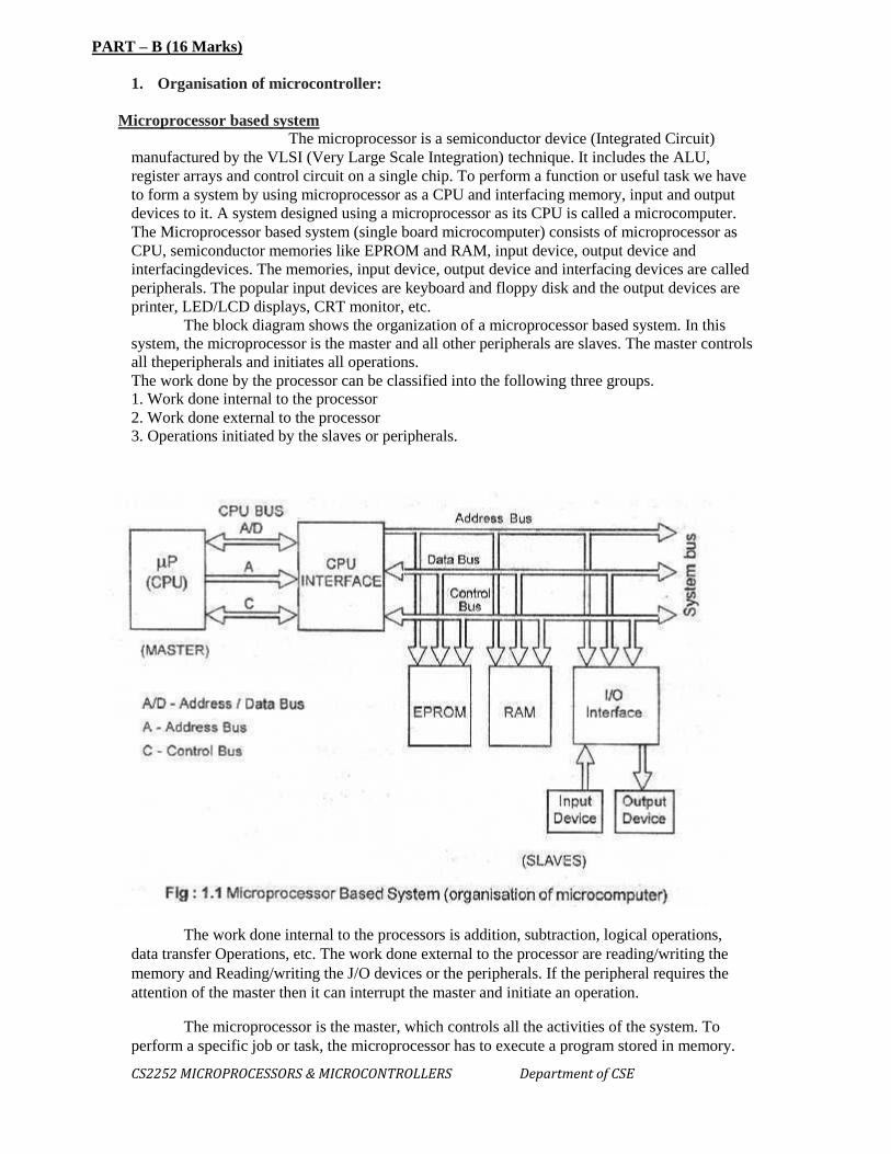
1. Organisation of microcontroller:
Microprocessor based system
The microprocessor is a semiconductor device (Integrated Circuit)
manufactured by the VLSI (Very Large Scale Integration) technique. It includes the ALU,
register arrays and control circuit on a single chip. To perform a function or useful task we have
to form a system by using microprocessor as a CPU and interfacing memory, input and output
devices to it. A system designed using a microprocessor as its CPU is called a microcomputer.
The Microprocessor based system (single board microcomputer) consists of microprocessor as
CPU, semiconductor memories like EPROM and RAM, input device, output device and
interfacingdevices. The memories, input device, output device and interfacing devices are called
peripherals. The popular input devices are keyboard and floppy disk and the output devices are
printer, LED/LCD displays, CRT monitor, etc.
The block diagram shows the organization of a microprocessor based system. In this
system, the microprocessor is the master and all other peripherals are slaves. The master controls
all theperipherals and initiates all operations. The work done by the processor can be classified into the following three groups. 1. Work done internal to the processor 2. Work done external to the processor 3. Operations initiated by the slaves or peripherals.
The work done internal to the processors is addition, subtraction, logical operations,
data transfer Operations, etc. The work done external to the processor are reading/writing the
memory and Reading/writing the J/O devices or the peripherals. If the peripheral requires the
attention of the master then it can interrupt the master and initiate an operation.
The microprocessor is the master, which controls all the activities of the system. To
perform a specific job or task, the microprocessor has to execute a program stored in memory.

CS2252 MICROPROCESSORS & MICROCONTROLLERS Department of CSE
The program consists of a set of instructions. It issues address and control signals and fetches the
instruction and data from memory. The instruction is executed one by one internal to the
processor and based on the result it takes appropriate action.
BUSES: The buses are group of lines that carries data, address or control signals. · The CPU Bus has multiplexed lines, i.e., same line is used to carry different signals . The CPU interface is provided to demultiplex the multiplexed lines, to generate chip
select signals and additional control signals. · The system bus has separate lines for each signal. All the slaves in the system are connected to the same system bus. At any time instant
communication takes place between the master and one of the slaves. All the slaves have
tristate logic and hence normally remain in high impedance state. Only when the slave is
selected it comes to the normal logic. PERIPHERAL DEVICES: · The EPROM memory is used to store permanent programs and data.
· The RAM memory is used to store temporary programs and data.
· The input device is used to enter the program, data and to operate the system. · The output device is used for examining the results.
Since the speed of I/O devices does not match with the speed of microprocessor, an
interface device is provided between system bus and I/O devices. Generally I/O devices are
slow devices. Advantages of Microprocessor based system 1. Computational/processing speed is high. 2. Intelligence has been brought to systems.
3. Automation of industrial processes and office administration. 4. Since the devices are programmable, there is flexibility to alter the system by changing
the softwarealone.
5. Less number of components, compact in size and cost less. Also it is more reliable. 6. Operation and maintenance are easier.
Disadvantages of Microprocessor based System 1. It has limitations on the size of data. 2. The applications are limited by the physical address space. 3. The analog signals cannot be processed directly and digitizing the analog signals
introduces errors. 4. The speed of execution is slow and so real time applications are not possible.
5. Most of the microprocessors does not support floating point operations.
2. Architecture of 8085 microprocessor:
The salient features of 8085 μp are: • It is a 8 bit microprocessor. • It is manufactured with N-MOS technology. • It has 16-bit address bus and hence can address up to 216 = 65536 bytes (64KB)
memory locations through A0-A15.
• The first 8 lines of address bus and 8 lines of data bus are multiplexed AD0 – AD7.
• Data bus is a group of 8 lines D0 – D7.
• It supports external interrupt request. • A 16 bit program counter (PC) • A 16 bit stack pointer (SP) • Six 8-bit general purpose register arranged in pairs: BC, DE, HL. • It requires a signal +5V power supply and operates at 3.2 MHZ single phase clock. • It is enclosed with 40 pins DIP (Dual in line package).

CS2252 MICROPROCESSORS & MICROCONTROLLERS Department of CSE
ARCHITECTURE: 8085 consists of various units and each unit performs its own functions. The various units of a microprocessor are listed below
Accumulator
Arithmetic and logic Unit
General purpose register
Program counter
Stack pointer
Temporary register
Flags
Instruction register and Decoder
Timing and Control unit
Interrupt control
Serial Input/output control
Address buffer and Address-Data buffer
Address bus and Data bus • Accumulator •
Accumulator is nothing but a register which can hold 8-bit data. Accumulator
aids in storing two quantities. The data to be processed by arithmetic and logic unit is
stored in accumulator. It also stores the result of the operation carried out by the
Arithmetic and Logic unit.The accumulator is also called an 8-bit register. The
accumulator is connected to Internal Data bus and ALU (arithmetic and logic unit). The
accumulator can be used to send or receive data from the Internal Data bus.
Arithmetic and Logic Unit There is always a need to perform arithmetic operations like +, -, *, / and to
perform logical operations like AND, OR, NOT etc. So there is a necessity for creating a separate unit which can perform such types of operations. These operations are performed by the Arithmetic and Logic Unit (ALU). ALU performs these operations on 8-bit data.
But these operations cannot be performed unless we have an input (or) data on which the desired operation is to be performed. So from where do these inputs reach the ALU? For this purpose accumulator is used. ALU gets its Input from accumulator and temporary register. After processing the necessary operations, the result is stored back in accumulator.

CS2252 MICROPROCESSORS & MICROCONTROLLERS Department of CSE
General Purpose Registers
These general purpose registers are used to hold data like any other registers. The general purpose registers in 8085 processors are B, C, D, E, H and L. Each register can hold 8-bit data. Apart from the above function these registers can also be used to work in pairs to hold 16-bit data. They can work in pairs such as B-C, D-E and H-L to store 16-bit data. The H-L pair works as a memory pointer. A memory pointer holds the address of a particular memory location. They can store 16-bit address as they work in pair.
Program Counter and Stack Pointer Program counter is a special purpose register. Consider that an instruction is being executed by processor. As soon as the ALU
finished executing the instruction, the processor looks for the next instruction to be executed. So, there is a necessity for holding the address of the next instruction to be executed in order to save time. This is taken care by the program counter. A program counter stores the address of the next instruction to be executed. In other words the program counter keeps track of the memory address of the instructions that are being executed by the microprocessor and the memory address of the next instruction that is going to be executed. Microprocessor increments the program whenever an instruction is being executed, so that the program counter points to the memory address of the next instruction that is going to be executed. Program counter is a 16-bit register. Stack pointer is also a 16-bit register which is used as a memory pointer. A stack is nothing but the portion of RAM (Random access memory).
Temporary Register: As the name suggests this register acts as a temporary memory during the
arithmetic and logical operations. Unlike other registers, this temporary register can only be accessed by the microprocessor and it is completely inaccessible to programmers. Temporary register is an 8-bit register. In the next article let us discuss about the
Flags
Timing and control unit
Interrupt control.
Flags: Flags are nothing but a group of individual Flip-flops. The flags are
mainly associated with arithmetic and logic operations. The flags will show either a logical (0 or 1) (i.e.) a set or reset depending on the data conditions in accumulator or various other registers. A flag is actually a latch which can hold some bits of information. It alerts the processor that some event has taken place.
Intel processors have a set of 5 flags.
Carry flag
Parity flag
Auxiliary carry flag
Zero flag
Sign flag.
Instruction Register and Decoder Instruction register is 8-bit register just like every other register of
microprocessor. Consider an instruction. The instruction may be anything like adding two data's, moving a data, copying a data etc. When such an instruction is fetched from memory, it is directed to Instruction register. So the instruction registers are specifically to store the instructions that are fetched from memory. There is an Instruction decoder which decodes the informations present in the
CS2252 MICROPROCESSORS & MICROCONTROLLERS Department of CSE
Instruction register for further processing.
Timing and Control Unit Timing and control unit is a very important unit as it synchronizes the
registers and flow of data through various registers and other units. This unit consists of an oscillator and controller sequencer which sends control signals needed for internal and external control of data and other units. The oscillator generates two-phase clock signals which aids in synchronizing all the registers of 8085 microprocessor.
Signals that are associated with Timing and control unit are:
Control Signals: READY, RD‟, WR‟, ALE
Status Signals: S0, S1, IO/M‟ DMA Signals: HOLD, HLDA
RESET Signals: RESET IN, RESET OUT
Interrupt Control As the name suggests this control interrupts a process. Consider that a
microprocessor is executing the main program. Now whenever the interrupt signal is enabled or requested the microprocessor shifts the control from main program to process the incoming request and after the completion of request, the control goes back to the main program. For example an Input/output device may send an interrupt signal to notify that the data is ready for input. The microprocessor temporarily stops the execution of main program and transfers control to I/O device. After collecting the input data the control is transferred back to main program. Interrupt signals present in 8085 are:
INTR
RST 7.5
RST 6.5
RST 5.5
TRAP Of the above four interrupts TRAP is a NON-MASKABLE interrupt
control and other three are maskable interrupts. A non-maskable interrupt is an interrupt which is given the highest priority in the order of interrupts. Suppose you want an instruction to be processed immediately, then you can give the instruction as a non-maskable interrupt. Further the non-maskable interrupt cannot be disabled by programmer at any point of time.Whereas the maskable interrupts can be disabled and enabled using EI and DI instructions. Among the maskable interrupts RST 7.5 is given the highest priority above RST 6.5 and least priority is given to INTR.
Serial I/O control The input and output of serial data can be carried out
using 2 instructions in 8085. SID-Serial Input Data SOD-Serial Output Data Two more instructions are used to perform serial-parallel conversion
needed for serial I/O devices. SIM
RIM
Address buffer and Address-Data buffer The contents of the stack pointer and program counter are loaded into the
address buffer and address-data buffer. These buffers are then used to drive the external address bus and address-data bus. As the memory and I/O chips are connected to these buses, the CPU can exchange desired data to the memory and

CS2252 MICROPROCESSORS & MICROCONTROLLERS Department of CSE
I/O chips.The address-data buffer is not only connected to the external data bus but also to the internal data bus which consists of 8-bits. The address data buffer can both send and receive data from internal data bus.
Address bus and Data bus: We know that 8085 is an 8-bit microprocessor. So the data bus present in
the microprocessor is also 8-bits wide. So 8-bits of data can be transmitted from or to the microprocessor. But 8085 processor requires 16 bit address bus as the memory addresses are 16-bit wide. The 8 most significant bits of the address are transmitted with the help of address bus and the 8 least significant bits are transmitted with the help of multiplexed address/data bus. The eight bit data bus is multiplexed with the eight least significant bits of address bus. The address/data bus is time multiplexed. This means for few microseconds, the 8 least significant bits of address are generated, while for next few seconds the same pin generates the data. This is called Time multiplexing. But there are situations where there is a need to transmit both data and address simultaneously. For this purpose a signal called ALE (address latch enable) is used. ALE signal holds the obtained address in its latch for a long time until the data is obtained and so when the microprocessor sends the data next time the address is also available at the output latch. This technique is called Address/Data
demultiplexing.
CS2252 MICROPROCESSORS & MICROCONTROLLERS Department of CSE
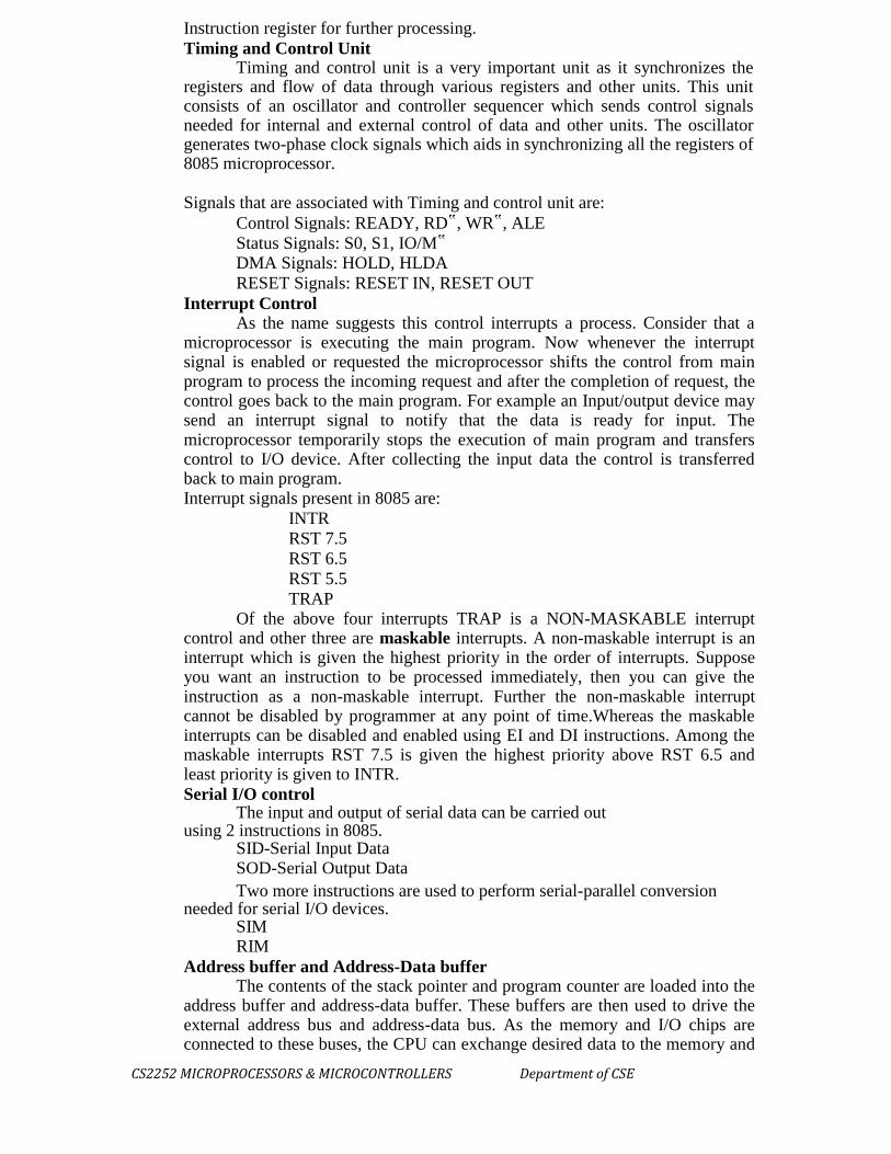
3. Pin configurations of 8085
8085 is a 40 pin IC, DIP package. The signals from the pins can be
grouped as follows
Power supply and clock signals
Address bus
Data bus
Control and status signals Interrupts and externally initiated signals
Serial I/O ports
Power supply and Clock frequency signals:
Vcc + 5 volt power supply
Vss Ground
X1, X2 : Crystal or R/C network or LC network connections to set the
frequency of internal clock generator.
The frequency is internally divided by two. Since the basic operating timing
frequency is 3
MHz, a 6 MHz crystal is connected externally.
CLK (output)-Clock Output is used as the system clock for peripheral

CS2252 MICROPROCESSORS & MICROCONTROLLERS Department of CSE
and devices interfaced with the microprocessor. Address Bus:
A8 - A15 (output; 3-state)
It carries the most significant 8 bits of the memory address or the 8 bits of
the I/O address;
Multiplexed Address / Data Bus:
AD0 - AD7 (input/output; 3-state)
These multiplexed set of lines used to carry the lower order 8 bit address as
well as data bus.
During the opcode fetch operation, in the first clock cycle, the lines deliver
the lower order address A0 - A7.
In the subsequent IO / memory, read / write clock cycle the lines are used as
data bus. The CPU may read or write out data through these lines.
Control and Status signals:
ALE (output) - Address Latch Enable.
This signal helps to capture the lower order address presented on the
multiplexed address /
data bus.
RD (output 3-state, active low) - Read memory or IO device.
This indicates that the selected memory location or I/O device is to be read
and that the data bus is ready for accepting data from the memory or I/O
device.
WR (output 3-state, active low) - Write memory or IO device.
This indicates that the data on the data bus is to be written into the selected
memory location or I/O device.
IO/M (output) - Select memory or an IO device.
This status signal indicates that the read / write operation relates to whether
the memory or
I/O device.
It goes high to indicate an I/O operation. It goes low for memory operations.
Status Signals:
It is used to know the type of current operation of the microprocessor.
4. Addressing modes:
Every instruction of a program has to operate on a data.
The method of specifying the data to be operated by the instruction is called Addressing.
The 8085 has the following 5 different types of addressing.
1. Immediate Addressing
2. Direct Addressing

CS2252 MICROPROCESSORS & MICROCONTROLLERS Department of CSE
3. Register Addressing
4. Register Indirect Addressing
5. Implied Addressing 1. Immediate Addressing:
In immediate addressing mode, the data is specified in the instruction itself. The
data will be a part of the program instruction.
EX. MVI B, 3EH - Move the data 3EH given in the instruction to B register; LXI SP,
2700H.
2. Direct Addressing: In direct addressing mode, the address of the data is specified in the instruction.
The data will be in memory. In this addressing mode, the program instructions and data
can be stored in different memory.
EX. LDA 1050H - Load the data available in memory location 1050H in to
accumulator; SHLD 3000H
3. Register Addressing: In register addressing mode, the instruction specifies the name of the register in
which the data is available.
EX. MOV A, B - Move the content of B register to A register; SPHL; ADD C.
4. Register Indirect Addressing: In register indirect addressing mode, the instruction specifies the name of the
register in which the address of the data is available. Here the data will be in memory
and the address will be in the register pair.
EX. MOV A, M - The memory data addressed by H L pair is moved to A register.
LDAX B.
5. Implied Addressing: In implied addressing mode, the instruction itself specifies the data to be
operated. EX. CMA - Complement the content of accumulator; RAL.
5. Instruction sets:
The 8085 instruction set can be classified into the following five functional headings. Group I - DATA TRANSFER INSTRUCTIONS:
Includes the instructions that moves ( copies) data between registers or
between memory locations and registers. In all data transfer operations the content of
source register is not altered. Hence the data transfer is copying operation. Ex: i) MOV A,B ii) LDA 4600 iii) LHLD 4200
Group II - ARITHMETIC INSTRUCTIONS:
Includes the instructions which performs the addition, subtraction,
increment or decrement operations. The flag conditions are altered after execution
of an instruction in this group. Ex: i) ADD B ii) SUB C iii) INR D iv) INX H
Group III - LOGICAL INSTRUCTIONS: The instructions which performs the logical operations like AND, OR, Exclusive-
OR, complement, compare and rotate instructions are grouped under this heading. The flag
conditions are altered after execution of an instruction in this group. Ex: i) ORA B ii) XRA A iii) RAR
Group IV - BRANCHING INSTRUCTIONS:
The instructions that are used to transfer the program control from one
memory location to another memory location are grouped under this heading. Ex: i) JZ 4200 ii) RST 7 iii) CALL 4300
Group V - MACHINE CONTROL INSTRUCTIONS:
Includes the instructions related to interrupts and the instruction used to halt
program execution. Ex: i) SIM ii) RIM iii) HLT

CS2252 MICROPROCESSORS & MICROCONTROLLERS Department of CSE
The 74 basic instructions of8085 are listed inTable. The opcode of each
instruction, size, machine cycles, number of T -state and the total number of instructions
in each type are also shown intable in next page. The instructions affecting the status flag
are listed in table followed

CS2252 – MICROPROCESSORS & MICROCONTROLLERS Department of CSE 3
CS2252 – MICROPROCESSORS & MICROCONTROLLERS Department of CSE 3
CS2252 – MICROPROCESSORS & MICROCONTROLLERS Department of CSE 3

CS2252 – MICROPROCESSORS & MICROCONTROLLERS Department of CSE 3
6. TIMING DIAGRAM for various machine cycles: The machine cycles are the basic operations performed by the processor, while
instructions are executed. The time taken for performing each machine cycle is expressed in
terms of Tstates. One T-state is the time period of one clock cycle of the microprocessor. The various machine cycles are
1. Opcode fetch …………….. - 4 / 6 T 2. Memory Read ……………. - 3 T
3. Memory Write ……………. - 3 T 4. I/O Read ………………….. - 3 T
5. I/O Write …………………. - 3 T 6. Interrupt Acknowledge …… - 6 / 12 T
7. Bus Idle …………………… - 2 / 3 T

CS2252 – MICROPROCESSORS & MICROCONTROLLERS Department of CSE 3
8. Programming in 8085: 8 Bit Addition:
LXI H 4000H : HL points 4000H MOV A, M : Get first operand INX H : HL points 4001H
ADD M : Add second operand
INX H : HL points 4002H
MOV M, A : Store result at 4002H
HLT : Terminate program execution
Flowchart
CS2252 – MICROPROCESSORS & MICROCONTROLLERS Department of CSE 3
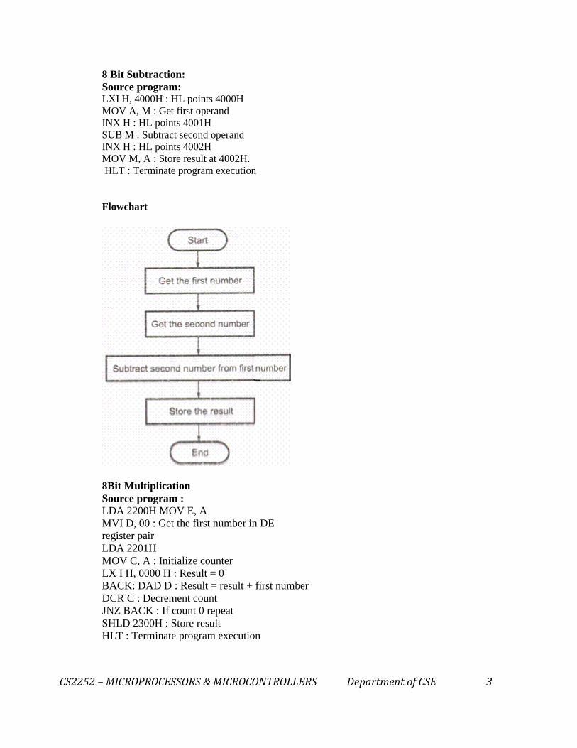
8 Bit Subtraction:
Source program: LXI H, 4000H : HL points 4000H
MOV A, M : Get first operand
INX H : HL points 4001H
SUB M : Subtract second operand
INX H : HL points 4002H
MOV M, A : Store result at 4002H.
HLT : Terminate program execution
Flowchart
8Bit Multiplication
Source program :
LDA 2200H MOV E, A
MVI D, 00 : Get the first number in DE
register pair
LDA 2201H
MOV C, A : Initialize counter
LX I H, 0000 H : Result = 0
BACK: DAD D : Result = result + first number
DCR C : Decrement count
JNZ BACK : If count 0 repeat
SHLD 2300H : Store result
HLT : Terminate program execution

CS2252 – MICROPROCESSORS & MICROCONTROLLERS Department of CSE 3
Flowchart
PROGRAMMING EXAMPLES: 1. Write an ALP using 8085 to multiply two 8-bit numbers by repeated addition. MVI A, OO ; Accumulator contents are cleared
MVI C, OO ; C Register contents are cleared
MVI B, data#1 ; I Operand is loaded into B Register
MVI D, data#2 ; II Operand is loaded into D Register
Loop: ADD B |
JNC next |
INR C } Multiplication by repeated addition.
Next: DCR D |
JNZ loop |
STA 4200H ; Storing of results into memory location
MOV A,C
Storing of carry into next memory location
STA 4201H ;

CS2252 – MICROPROCESSORS & MICROCONTROLLERS Department of CSE 3
2. Write an ALP using 8085 to evaluate the expression C=A2+B2 Let ‘A’ be Data#1 and ‘B’ be Data#2 MVI B, Data#1 ; Data #1 is stored in register B MOV C, B ; Copy of Data #1 is made in register C MVI D, Data#2 ; Data #2 is stored in register D MOV E,D ; Copy of Data #2 is made in register E XRA A ; Accumulator content is cleared Again: ADD B ] DCR C } A2 is calculated by repeated Addition JNZ Again ] MOV H,A ; Calculated A2 value is stored in register H XRA A ; Accumulator content is cleared Loop: ADD D ] DCR E } B2 is calculated by repeated Addition JNZ Loop ] ADD H ; A2+ B2 is determined,
by adding result in A
and register content H STA 4200H ; Result is stored in memory location 4200H