UNIT 1: DIODES AND CIRCUITS - Websmemberfiles.freewebs.com/69/76/88837669/documents/... · UNIT 1:...
27
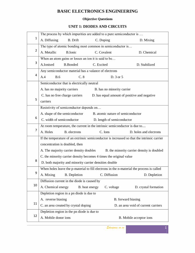
Eduspace.co.in 1 BASIC ELECTRONICS ENGINEERING Objective Questions UNIT 1: DIODES AND CIRCUITS 1 The process by which impurities are added to a pure semiconductor is … A. Diffusing B. Drift C. Doping D. Mixing 2 The type of atomic bonding most common in semiconductor is… A. Metallic B.Ionic C. Covalent D. Chemical 3 When an atom gains or losses an ion it is said to be… A.Ionised B.Bonded C. Excited D. Stabilized 4 Any semiconductor material has a valance of electrons A.4 B.6 C. 8 D. 3 or 5 5 Semiconductor that is electrically neutral A. has no majority carriers B. has no minority carrier C. has no free charge carriers D. has equal amount of positive and negative carriers 6 Resistivity of semiconductor depends on… A. shape of the semiconductor B. atomic nature of semiconductor C. width of semiconductor D. length of semiconductor 7 At room temperature, the current in the intrinsic semiconductor is due to.... A. Holes B. electrons C. Ions D. holes and electrons 8 If the temperature of an extrinsic semiconductor is increased so that the intrinsic carrier concentration is doubled, then A. The majority carrier density doubles B. the minority carrier density is doubled C. the minority carrier density becomes 4 times the original value D. both majority and minority carrier densities double 9 When holes leave the p-material to fill electrons in the n-material the process is called A. Mixing B. Depletion C. Diffusion D. Depletion 10 Diffusion current in the diode is caused by A. Chemical energy B. heat energy C. voltage D. crystal formation 11 Depletion region in a pn diode is due to A. reverse biasing B. forward biasing C. an area created by crystal doping D. an area void of current carriers 12 Depletion region in the pn diode is due to A. Mobile donor ions B. Mobile acceptor ions
Transcript of UNIT 1: DIODES AND CIRCUITS - Websmemberfiles.freewebs.com/69/76/88837669/documents/... · UNIT 1:...
Eduspace.co.in 1
BASIC ELECTRONICS ENGINEERING
Objective Questions
UNIT 1: DIODES AND CIRCUITS
1 The process by which impurities are added to a pure semiconductor is …
A. Diffusing B. Drift C. Doping D. Mixing
2 The type of atomic bonding most common in semiconductor is…
A. Metallic B.Ionic C. Covalent D. Chemical
3 When an atom gains or losses an ion it is said to be…
A.Ionised B.Bonded C. Excited D. Stabilized
4 Any semiconductor material has a valance of electrons
A.4 B.6 C. 8 D. 3 or 5
5
Semiconductor that is electrically neutral
A. has no majority carriers B. has no minority carrier
C. has no free charge carriers D. has equal amount of positive and negative
carriers
6
Resistivity of semiconductor depends on…
A. shape of the semiconductor B. atomic nature of semiconductor
C. width of semiconductor D. length of semiconductor
7 At room temperature, the current in the intrinsic semiconductor is due to....
A. Holes B. electrons C. Ions D. holes and electrons
8
If the temperature of an extrinsic semiconductor is increased so that the intrinsic carrier
concentration is doubled, then
A. The majority carrier density doubles B. the minority carrier density is doubled
C. the minority carrier density becomes 4 times the original value
D. both majority and minority carrier densities double
9 When holes leave the p-material to fill electrons in the n-material the process is called
A. Mixing B. Depletion C. Diffusion D. Depletion
10 Diffusion current in the diode is caused by
A. Chemical energy B. heat energy C. voltage D. crystal formation
11
Depletion region in a pn diode is due to
A. reverse biasing B. forward biasing
C. an area created by crystal doping D. an area void of current carriers
12 Depletion region in the pn diode is due to
A. Mobile donor ions B. Mobile acceptor ions

Eduspace.co.in 2
C. Mobile donor and acceptor ions D. majority carriers
13
When a diode is forward biased
A. Barrier potential increases B. Barrier potential decreases
C. Majority current reduces D. Minority current reduces
14 Barrier potential for silicon diode
A.0.3 V B.0.4 V C.0.1 V D.0.7 V
15
A strong electric field across a P-N junction that causes covalent bond to break apart is
called
A. avalanche breakdown B. reverse breakdown
C. lever breakdown D. low voltage breakdown
16
When thermally generated holes and electrons gain enough energy from the reverse
biased source of a zener diode to produce a new current carriers is called
A. avalanche breakdown B. reverse breakdown
C. zener breakdown D. low voltage breakdown
17 The p-n junction forms device called
A. Triac B. Diode C. multiplexer D. semiconductor
18 Practically depletion region is of the order of
A. Meters B. centimeters C. Microns D. millimeters
19 1 micron =
A. 1 x 10 -6 m B. 1 x 10
-6 cm C. 1 x 10
-3 m D. 10 x 10
-3 m
20 Barrier potential for germanium diode
A.0.3 V B.0.4 V C.0.1 V D.0.7 V
21
If an external dc voltage is applied in such a way that p- region terminal is connected to
positive , the biasing condition is
A. Unbiased B. reverse biased C. forward biased D. all of the above
22 Due to forward bias voltage width of Depletion region
A. Enhances B. narrows C. remain same D. none of the above
23 The normal forward biased operation of diode is
A. Below the knee point B. at the origin C. above knee point D. all the above
24. If an external dc voltage is applied in such a way that p- region terminal is connected to
negative , the biasing condition is
A. Unbiased B. reverse biased C. forward biased D. all of the above
25 In diode reverse current is due to

Eduspace.co.in 3
A. Mobile donor ions B. Mobile acceptor ions
C. minority carriers D. majority carriers
26
The reverse breakdown of diode occurs due to
A. Avalanche effect B. Zener effect C. heat effect D. both A and B
27 Reverse characteristic of diode is plotted in
A. 1st Quadrant B. 2
nd Quadrant C. 3
rd Quadrant D. 4
th Quadrant
28 Rectifier converts
A. a.c. voltage to d.c.voltage B. a.c voltage to pulsating d.c voltage
C. d.c voltage to a.c. voltage D. a.c voltage to a.c voltage
29. The manufacturer of diode provides the detail information about diode, in the form of
A. excel sheet B. data sheet C. log sheet D. none of the above
30. The amount of a.c. content in the output of rectifier is called
A. form factor B. peak factor C. ripple factor D. knee factor
31. Efficiency of half wave rectifier is
A. 81.2 % B. 40.6 % C. 45.6 % D. 82.1 %
32. Ripple factor of half wave rectifier is
A. 2.122 B. 1.112 C. 1.211 D. 2.11
33. Efficiency of full wave rectifier is
A. 81.2 % B. 40.6 % C. 45.6 % D. 82.1 %
34. Ripple factor of full wave rectifier is
A. 0.122 B. 0.4 C. 0.48 D. 0.05
35. Efficiency of bridge rectifier is
A.81.2 % B. 40.6 % C. 45.6 % D. 82.1 %
36. Ripple factor of bridge rectifier is
A. 0.122 B. 0.4 C. 0.48 D. 0.05
37. To minimize the ripple content in the circuit
A. Diode circuit is used B. filter circuit is used
C. bridge circuit is used D. none of the above
38. Types of filter are
A. Capacitor input filter B. choke input filter C. resister input filter
D. both A and B
39. The zener diode is generally operated in
A. Forward breakdown region B. reverse breakdown region C. middle breakdown
region D. all above
40. Practically zener diodes are operated in
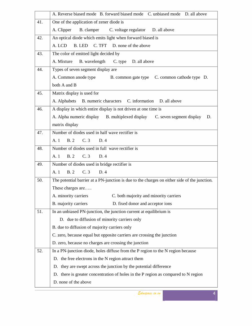
Eduspace.co.in 4
A. Reverse biased mode B. forward biased mode C. unbiased mode D. all above
41. One of the application of zener diode is
A. Clipper B. clamper C. voltage regulator D. all above
42. An optical diode which emits light when forward biased is
A. LCD B. LED C. TFT D. none of the above
43. The color of emitted light decided by
A. Mixture B. wavelength C. type D. all above
44. Types of seven segment display are
A. Common anode type B. common gate type C. common cathode type D.
both A and B
45. Matrix display is used for
A. Alphabets B. numeric characters C. information D. all above
46. A display in which entire display is not driven at one time is
A. Alpha numeric display B. multiplexed display C. seven segment display D.
matrix display
47. Number of diodes used in half wave rectifier is
A. 1 B. 2 C. 3 D. 4
48. Number of diodes used in full wave rectifier is
A. 1 B. 2 C. 3 D. 4
49. Number of diodes used in bridge rectifier is
A. 1 B. 2 C. 3 D. 4
50. The potential barrier at a PN-junction is due to the charges on either side of the junction.
These charges are…..
A. minority carriers C. both majority and minority carriers
B. majority carriers D. fixed donor and acceptor ions
51. In an unbiased PN-junction, the junction current at equilibrium is
D. due to diffusion of minority carriers only
B. due to diffusion of majority carriers only
C. zero, because equal but opposite carriers are crossing the junction
D. zero, because no charges are crossing the junction
52. In a PN-junction diode, holes diffuse from the P region to the N region because
D. the free electrons in the N region attract them
D. they are swept across the junction by the potential difference
D. there is greater concentration of holes in the P region as compared to N region
D. none of the above

Eduspace.co.in 5
53. In a PN-junction diode, if the junction current is zero, this means that
D. the potential barrier has disappeared
D. there are no carriers crossing the junction
D. the number of majority carriers crossing the junction equals the number of
minority carriers crossing the junction
D. the number of holes diffusing from the P region equals the number of electrons
diffusing from the N region
54. In a semiconductor diode, the barrier potential offers opposition to only
D. majority carriers in both regions
B. minority carriers in both regions
C. free electrons in the N region
D. holes in the P region
55. When we apply reverse bias to a junction diode, it
D. lowers the potential barrier
D. raises the potential barrier
D. greatly increases the minority-carrier current
D. greatly increases the majority-carrier current
56. The number of minority carriers crossing the junction of a diode depends primarily on
the
D. concentration of doping impurities
D. magnitude of the potential barrier
D. magnitude of the forward-bias voltage
D. rate of thermal generation of electron –hole pairs
57. The reverse saturation current in a junction diode is the current that flows when
D. only majority carriers are crossing the junction
D. only minority carriers are crossing the junction
D. the junction is unbiased
D. the potential barrier is zero
58. When forward bias is applied to a junction diode, it
D. increases the potential barrier
D. decreases the potential barrier
C. reduces the majority-carrier current to zero
D. reduces the minority-carrier current to zero
59. The depletion or space –charge region in a junction diode contains charges that are
D. mostly majority carriers

Eduspace.co.in 6
D. mostly minority carriers
D. mobile donor and acceptor ions
D. fixed donor and acceptor ions
60. Avalanche breakdown in a semiconductor diode occurs when
D. forward current exceeds a certain value
D. reverse bias exceeds a certain value
C. forward bias exceeds a certain value
D. the potential barrier is reduced to zero
61. When a PN-junction is biased in the forward direction
D. only holes in the P region are injected into the N region
D. only electrons in the N region are injected into the P region
D. majority carriers in each region are injected into the other region
D. no carriers move
62. The forward bias applied to a PN- junction diode is increased from zero to higher values.
Rapid increase in the current flow for a relatively small increase in voltage occurs
D. immediately
D. only after the forward bias exceeds the potential barrier
C. when the flow of minority carriers is sufficient to cause an avalanche breakdown
D. when the depletion area becomes larger than the space-charge area
63. The capacitance of a reverse biased PN-junction
A. increases as the reverse bias is decreased
B. increases as the reverse bias is increased
C. depends mainly on the reverse saturation current
D. makes the PN-junction more effective at high frequencies
64. In a half-wave rectifier, the load current flows for
A. the complete cycle of the input signal
B. only for the positive half-cycle of the input signal
C. less than half cycle of the input signal
D. more than half cycle but less than the complete cycle of the input signal
65. In a full-wave rectifier, the current in each of the diodes flows for
A. the complete cycle of the input signal
B. half cycle of the input signal
C. less than half cycle of the input signal
D. zero time

Eduspace.co.in 7
66. In a half-wave rectifier, the peak value of the ac voltage across the secondary of the
transformer is 20√2 V. If no filter circuit is used, the maximum dc voltage across the load
will be
A. 28.28 V B. 14.14 V C. 20 V D. 9 V
67. If Vm is the peak voltage across the secondary of the transformer in a half-wave
rectifier(without any filter circuit), then the maximum voltage on the reverse biased diode
is
A. Vm B. ½. Vm C. 2 Vm D. none of the above
68. If Vm is the peak voltage across the secondary of the transformer in a half-wave rectifier
with a shunt capacitor filter circuit, then the maximum voltage on the reverse biased
diode is
A. Vm B. ½. Vm C. 2 Vm D. none of the above
69. In a centre-tap full-wave rectifier, Vm is the peak voltage between the centre-tap and one
end of the secondary. The maximum voltage across the reverse biased diode is
A. Vm B. ½. Vm C. 2 Vm D. none of the above
70. A zener diode………
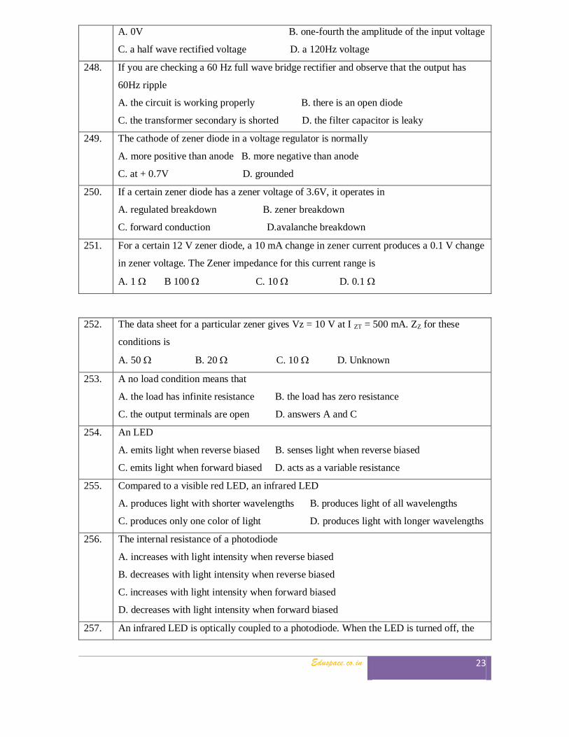
A. has a high forward-voltage rating B. has a sharp breakdown at low reverse
voltage C. is useful as an amplifier D. has a negative resistance
71. The light-emitting diode (LED)………
A. is usually made from silicon
B. uses a reverse-biased junction
C. gives a light output which increases with increase in temperature
D. depends on the recombination of holes and electrons
72. The resistivity of a semiconductor…………………conductors and insulators.
A. is more than that of B. lies between that of
C. is less than that of D. none of the above
73. A semi-conductor is formed by………… bonds.
A. covalent B. electrovalent C. co-ordinate D. none of the above
74. The most commonly used semi-conductor is…….
A. germanium B. carbon C. sulpher D. silicon
75. In a semiconductor, the energy gap between valence band and conduction band is
about………

Eduspace.co.in 8
A. 5 eV B. 10 eV C. 15 eV D. 1 eV
76. A semiconductor has ………temperature coefficient of resistance.
A. negative B. positive C. zero D. none of the above
77. A semiconductor generally has……… valence electrons.
A. 2 B. 3 C. 4 D. 6
78. The resistivity of pure germanium under standard conditions is about……..
A. 6*104 Ω-cm B. 60 Ω-cm C. 3*10
-3 Ω-cm D. 6*10
-4 Ω-cm
79. The resistivity of pure silicon is about……….
A. 100 Ω-cm B. 6000 Ω-cm C. 3*106 Ω-cm D. 1.6* 10
-8 Ω-cm
80. When a pure semi-conductor is heated, its resistance……….
A. goes down B. goes up C. remains the same D. none of the above
81. The strength of a semiconductor crystal comes from…………
A. forces between nuclei B. forces between protons
C. electron-pair bonds D. none of the above
82
When a pentavalent impurity is added to a pure semi-conductor, it becomes………
semiconductor.
A. intrinsic B. n-type C. p-type D. none of the above
83 Addition of pentavalent impurity to a semiconductor creates many………
A. free electrons B. holes C. valence electrons D. bound electrons
84
A pentavalent impurity has……..
A. 3 valence electrons B. 6 valence electrons
C. 4 valence electrons D. 5 valence electrons
85 An n-type semiconductor is……..
A. positively charged B. electrically neutral C. negatively charged D. none of the above
86
A trivalent impurity has………
A. 3 valence electrons B. 5 valence electrons C. 6 valence electrons D. 4 valence
electrons
87 Addition of trivalent impurity to a pure semiconductor creates many……….
A. free electrons B. valence electrons C. holes D. bound electrons
88
A hole in a semi-conductor is defined as…….
A. a free electron B. the incomplete part of an electron pair bond
C. a free proton D. a free neutron
89 A pentavalent impurity is called……

Eduspace.co.in 9
A. donor impurity B. acceptor impurity C. ionic impurity D. none of the above
90
The charge of a hole is………
A. zero B. equal to that of a proton C. equal to that of an electron D. equal to that
of a neutron
91 As a general rule, holes are found only in……….
A. metals B. semiconductors C. insulators D. resistance materials
92
A semiconductor diode has……..
A. two pn junctions B. one pn junction
C. three pn junctions D. none of the above
93 A semiconductor diode has forward resistance of the order of ……….
A. Ω B. K Ω C. M Ω D. none of the above
94
If the arrow of a semiconductor diode symbol is positive w.r.t. bar, then diode is…..biased.
A. revere B. forward C. none of the two D. forward or reverse
95 The reverse current in a diode is of the order of …………….
A. µA B. mA C. A D. KA
96 The forward voltage drop across a silicon diode is about…………..
A. 2.5 V B. 3 V C. 0.7 V D. 10 V
97 A semiconductor diode is used as………..
A. an amplifier B. a rectifier C. an oscillator D. a voltage regulator
98 The dc resistance of a semiconductor diode is ….. that of its ac resistance.
A. the same as B. more than C. less than D. none of the above
99
An ideal semiconductor diode is one which behaves as a perfect………… when forward
biased.
A. conductor B. insulator C. resistance material D. none of the above
100
The reverse resistance and forward resistance of a semiconductor diode have a ratio of
about…..
A. 1:1 B. 1000:1 C. 100:1 D. 2:1
101 The leakage current in a semiconductor diode is due to…….
A. minority carriers B. majority carriers C. junction capacitance D. none of the above
102 If temperature of a semiconductor diode increases, leakage current…………………
A. remains the same B. decreases C. increases D. becomes zero
103
The PIV rating of a semiconductor diode is …………… that of equivalent vacuum
diode.
A. lower than B. more than C. the same as D. none of the above

Eduspace.co.in 10
104 If the doping level of a semiconductor diode is increased, the breakdown voltage……..
A. remains the same B. is decreased C. is increased D. none of the above
105 A semiconductor diode is a……….. device.
A. non-linear B. linear C. amplifying D. none of the above
106 A semiconductor diode utilizes…………….. characteristic for rectification.
A. reverse B. forward C. forward or reverse D. none of the above
107
When a semiconductor diode is used as a rectifier, the most important consideration
is……………..
A. doping level B. PIV C. forward resistance D. none of the above
108
If doping level in a semiconductor diode is increased, the width of depletion
leyer………..
A. remains the same B. is increased C. is decreased D. none of the above
109 A zener diode has…………..
A. one pn-junction B. two pn-junctions C. three pn-junctions D. none of the above
110 A zener diode is used as………
A. an amplifier B. a rectifier C. a voltage regulator D. a multivibrator
111 The doping level in a zener diode is ….. that of a semiconductor diode.
A. more than B. less than C. the same as D. none of the above
112
A pure semiconductor is often referred to as……….
A. extrinsic semiconductor B. intrinsic semiconductor
C. doped semiconductor D. none of the above
113
An n-type semiconductor is a semiconductor that has been doped with……….
A. trivalent impurity atoms B. impurity atoms whose electron
valence is +4
C. pentavalent impurity atoms D. none of the above
114 For a silicon diode, the barrier potential is approximately…………..
A. 0.7 V B. 0.3 V C. 2.0 V D. 6.8 V
115 . In a p-type semiconductor, the majority current carriers are…………
A. free electrons B. valence electrons C. protons D. holes
116
To forward bias a diode,……
A. the anode voltage must be positive with respect to its cathode
B. the anode voltage must be negative with respect to its cathode
C. the cathode voltage must be positive with respect to its anode

Eduspace.co.in 11
D. either a or b
117 A reverse-biased diode acts like………..
A. closed switch B. open switch C. small resistance D. none of the above
118 The sharing of valence electrons in a silicon crystal is called…..
A. doping B. the avalanche effect C. covalent bonding D. coupling
119 When used as a voltage regulator, a zener diode is normally………….
A. forward-biased B. reverse- biased C. not biased D. none of the above
120 In an n-type semiconductor, the minority current carriers are………….
A. free electrons B. protons C. valence electrons D. holes
121
A p-type semiconductor is a semiconductor doped with…….. A. trivalent impurity atoms B. impurity atoms whose electron valence is +4
C. pentavalent impurity atoms D. none of the above
122
To a first approximation, a forward-biased diode is treated like a………
A. open switch with infinite resistance
B. closed switch with a voltage drop of 0V
C. closed switch in series with a battery voltage of 0.7 V
D. closed switch in series with a small resistance and a battery
123
What is the dc output voltage of an unfiltered half-wave rectifier whose peak output
voltage is 9.8 V?
A. 6.23 V B. 19.6 V C. 9.8 V D. 3.1 V
124
What is the frequency of the capacitor ripple voltage in a full-wave rectifier circuit if the
frequency of the transformer secondary voltage is 60 Hz?
A. 60Hz B. 50 Hz C. 120 Hz D. this is impossible to determine
125
In a full-wave rectifier, the dc load current equals 1A. How much dc current is carried by
each diode?
A. ½ A B. 1 A C. 2 A D. 0 A
126 A 12 V zener diode has a 1W power rating. What is the maximum rated zener current?
A. 120 mA B. 83.3 mA C. 46.1 mA D. 1A
127
In a loaded zener regulator, the series resistor has a current, Is of 120 mA. If the load
current IL is 45 mA, how much is the zener current IZ?
A. 45 mA B. 165 mA C. 75 mA D. this is impossible to determine
128 The approximate voltage drop across a forward- biased LED is
A. 0.3 V B. 0.7 V C. 5.6 V D. 2.0 V
129 The output from an unfiltered half-wave or full wave rectifier is --
A. a pulsating dc voltageB. steady dc voltage C. smooth dc voltageD. none of the above

Eduspace.co.in 12
130 A diode is a…..
A. unidirectional device B. linear device C. nonlinear device D. both a and c
131
What is the approximate dc output voltage from a filtered bridge rectifier whose peak
output voltage is 30V?
A. 19.1 V B. 9.5 V C. 30 V D. none of the above
132
LEDs have replaced incandescent lamps in many applications because they have…….
A. a lower operating voltage B. a longer life C. faster on-off switching D. all the
advantages as a, b,c,d
133
Silicon diodes are preferred to germanium diodes for high temperature operation because
A. rate of increase of reverse saturation current with temperature is more in case of
silicon
B. doping of silicon is a simple process
C. the reverse saturation current of silicon diodes is smaller than that of germanium
D. none of the above
134
In an unbiased P-N junction, the current in equilibrium is
A. due to diffusion of minority carriers
B. zero, because no charges cross the junction
C. zero, because equal number of charges cross the junction
D. due to diffusion of majority carriers
135
In intrinsic semiconductor, the free electron concentration depends on
A. effective mass of holes only B. effective mass of electrons only
C. temperature of the semiconductor D. none of the above
136
In a forward biased P-N junction, the diffusion capacitance varies as
A. inversely with the current B. as the square of the current
C. linearly with the current D. as the square root of the current
137
In a PN-junction the diffusion capacitance
A. decreases with decreasing current and increasing temperature
B. decreases with increasing current and increasing current
C. increases with increasing current and increasing temperature
D. does not depend on current and temperature
138
A half wave rectified sinusoidal waveform has a peak voltage of 12V. Its average value
and rms value of the fundamental components are; respectively given by
A. 15/ V, 7.5 V B. 20/ V, 10/2 V C. 12/ V, 6 V D. none of these

Eduspace.co.in 13
139
In a zener diode,….
A. only N-region is heavily doped B. only P-region is heavily doped
C. both P and N-regions are heavily doped D. both P and N-regions are lightly doped
140
In a P-type semiconductor
A. electrons are the majority carriers
B. the hole concentration is less than the electron concentration
C. electron density does not change with temperature
D. at room temperature, the hole concentration equals the acceptor concentration
141
A zener diode is operated in the following mode as a voltage stabilizer
A. reverse bias B. forward bias
C. beyond the breakdown region D. reverse bias around the knee of breakdown region
142
Select the doping agent so that the intrinsic semiconduction silicon will be P-type
silicon:
A. phosphorous B. gallium C. boron D. arsenic
143
A general purpose diode is more likely to suffer avalanche breakdown rather than zener
breakdown because
A. its leakage current is small B. it has weak covalent bonds
C. it is lightly doped D. it has low reverse resistance
144 The turn-on voltage of a Ge junction diode is nearly….. volts.
A. 0.7 B. 0.3 C. 1.0 D. 0.1
145
The peak inverse voltage(PIV) is the maximum reverse voltage that can be applied to
diode without…
A. burnout B. destruction C. overheating D. charring
146
Leakage current of a junction diode…..
A. decreases with temperature B. is due to majority carriers
C. depends on the method of its fabrication D. is in the range of mA or µA
147 In the forward region of its characteristic ; a diode appears as
A. an OFF switch B. a high resistance C. a capacitor D. an ON switch
148
Under small signal operation of a diode
A. its bulk resistance increases B. its junction resistance predominates
C. it acts like a closed switch D. it behaves as a clipper
149
The value of Zener current is….
A. limited by external circuit resistance B. determined by zener voltage
C. totally independent of temperature D. always in µA range
150 When used in a circuit, the zener diode is always…….

Eduspace.co.in 14
A. forward biased B. connected in series C. troubled by overheating D. reverse biased
151 Once a zener diode goes into breakdown, its ……….doesn’t change much.
A. voltage B. current C. dynamic impedance D. capacitance
152
The main reason why electrons can tunnel through a P-N junction is that..
A. they have high energy B. barrier potential is very low
C. depletion layer is extremely thin D. impurity level is low
153
The colour of light emitted by a LED depends on…
A. its forward bias B. its reverse bias
C. the amount of forward current D. the type of semiconductor material used
154 N-type germanium is obtained on doping intrinsic germanium by
A. Phosphorous B. Aluminium C. Boron D. Gold
155
Depletion region is a zone which contains
A. Holes only B. Electrons only
C. both electrons and holes D. ions only
156
In a semiconductor diode, arrow represents
A. n-type material B. p-type material
C. both p and n-type materials D. none of the above
157 Zener diode is used for
A. rectification B. amplification C. voltage stabilization D. current stabilization
158
If a pure silicon crystal has one million free electrons inside it, how many holes does it
have?
A. One million B. two million C. zero D.ten million
159
Assuming a barrier potential of 0.7 volts at an ambient temperature of 25 C, what is the
barrier potential of a silicon diode when the junction temperature is 100C?
A. 0.7 V B. 0.55 V C. 0.9 V D. 1V
160
The depletion region of a junction diode is formed
A. under forward biased B. when the temperature of the junction is reduced
C. under reverse biased D. under zero biased
161
The width of depletion layer of a junction
A. is independent of applied voltage B. is increased under reverse bias
C. decreases with light doping D. increases with heavy doping
162 The merging of free electrons and holes is called
A. lifetime B. covalent bonding C. recombination D. thermal energy
163 The voltage where avalanche occurs is called the
A. barrier potential B. depletion layer C. knee voltage D. breakdown voltage

Eduspace.co.in 15
164 Surface leakage current is part of the
A. reverse current B. reverse breakdown C. forward current D. forward breakdown
165
The voltage across diode in a full wave rectifier having input voltage of peak value Vm ,
during its non conducting period is
A. 0 B. –Vm C. -2Vm D. -4Vm
166
In a bridge rectifier circuit we use
A. no centre-tapping and diode having peak inverse voltage Vm
B. no centre tapping and diode having inverse voltage 2Vm
C. centre tapping and diode having reverse voltage Vm
D. centre- tapping and diode having reverse voltage 2Vm
167
In a full wave rectifier with R-C filter, the conduction angle of the diode is
A. 0 B. less than C. equal to D. More than
168 In an L-C filter the value of inductance is so chosen that it is approximately equal to
A. RL B. RL/2 C. RL/900 D. RL/10000
169
The no load voltage in a full wave rectifier with filter is
A. 2Vm/ B. Vm/ C. Vm D. 3Vm/2
170
PN junction is formed when P type semiconductor and N type semiconductor are joined
A. Togather B. Physically C. to get homogeneous material chemically
D. in such a manner that electrons and holes diffuse to give depletion layer
171
The depletion region of a junction diode is formed
A. when forward bias is applied to it B. when the temperature of the junction is
reduced
C. under reverse bias D. during manufacturing process
172
The width of the depletion layer of a junction
A. is independent of applied voltage B. is increased under reverse biased
C. decreases with light doping D. increases with heavy doping
173
The capacitor filter is characterized by
A. poor voltage regulation and high peak current capability
B. poor voltage regulation and low peak current capability
C. good voltage regulation and high peak current capability
D. good voltage regulation and low peak current capability
174 How many valance electrons does a silicon atom have?
A. 0 B. 1 C. 2 D. 4
175 Which is the most widely used semiconductor?
A. copper B. Germaniun C. Silicon D. None of the above

Eduspace.co.in 16
176 How many protons does the nucleus of a silicon atom contain?
A. 4 B. 14 C. 29 D. 32
177 Silicon atoms combine into an orderly pattern called
A. covalent bond B. crystal C. semiconductor D. valance orbit
178
An intrinsic semiconductor have some holes in it at room temperature what causes these
holes?
A. doping B. free electrons C. thermal energy D. valance electronics
179
When an electron is moved to an higher orbit level its energy level with respect to
nucleus
A. increases B. decreases C. remains the same D. depends on the type of atom
180 The merging of a free electrons and a hole is called as
A. covalent bonding B. lifetime C. recombination D. thermal energy
181 At room temperature an intrinsic silicon crystal acts approximately like
A. A battery B. A conductor C. An insulator D. a piece of copper wire
182 The amount of time between creation of a hole and its disappearance is called
A. doping B. lifetime C. recombination D. valance
183 The valance electron of a conductor can also be called a
A. bound electron B. free electron C. nucleus D. proton
184
When a voltage is applied to an semiconductor, holes will flow
A. away from the negative potential B. towards the positive potential
C. in the external circuit D. none of the above
185
For a semiconductor material, its valance orbit is saturated when it contains
A. 1 electrons B. equal positive and negative ions
C. 4 electrons D. 8 electrons
186
In an intrinsic semiconductor the number of holes
A. equals the number of free electrons
B. is greater than the number of free electrons
C. is less than the number of free electrons
D. none of the above
187 Absolute zero temperature equals
A. -2730C B. 0
0C C. 25
0C D. 50
0C
188
At absolute zero temperature an intrinsic semiconductor has
A. a few free electrons B. many holes
C. many free electrons D. no holes or free electrons
189 At room temperature an intrinsic semiconductor has

Eduspace.co.in 17
A. a few free electrons and holes B. many holes
C. many free electrons D. no holes
190
The number of free electrons and holes in an intrinsic semiconductor decreases when the
temperature
A. decreases B. increases C. stays the same D. none of the above
191 the flow of valance electrons to the right means that holes are flowing to the
A. left B. right C. either way D. none of the above
192 Holes act like
A. atoms B. crystals C. negative charges D. positive charges
193 Trivalent atoms have how many valance electronics
A. 1 B. 3 C. 4 D. 5
194 An accepter atom has how many valance electrons
A. 1 B. 3 C. 4 D. 5
195 If you wanted to produce an N type semiconductor which of these would you use?
A. acceptor atoms B. donor atom C. pentavalent impurity D. silicon
196 Electrons are the minority carriers in which type of semiconductor?
A. extrinsic B. intrinsic C. N type D. P type
197
How many free electrons does a p type semiconductor contain?
A. many B. None
C. only those produced by thermal energy D. same number as holes
198 Silver is the best conductor. How many valance electrons do you think it has?
A. 1 B. 4 C. 18 D. 29
199
Suppose an intrinsic semiconductor has 1 billion free electrons at room temperature. If
the temperature drops to 00C, how many holes are there?
A. fewer than 1 billion B. 1 billion C. more than 1 billion D. impossible to say
200
An external voltage source is applied to a p type semiconductor. If the left end of the
crystal is positive, which way do the majority carriers flow
A. left B. right C. neither D. impossible to say
201 Which of the following doesn’t fit in the group?
A. conductor B. semiconductor C. 4 valance electrons D. crystal structure
202 Which of the following is approximately equal to room temperature?
A. 00C b. 25
0C C. 50
0C D. 75
0C
203 Every known element has

Eduspace.co.in 18
A. the same type of atoms
B. the same number of atoms
C. a unique type of atom
D. several different types of atoms
204
An atom consists of
A. one nucleus and only one electron B. one nucleus and one or more electrons
C. protons, electrons and neutrons D. answers B and C
205
The nucleus of an atom is made up of
A. protons and neutrons B. electrons
C. electrons and protons D. electrons and neutrons
206 The valance shell in a silicon atom has the number designation of
A. 0 B. 1 C. 2 D. 3
207
Valance electrons are
A. in the closest orbit to the nucleus
B. in the most distant orbit from the nucleus
C. in various orbits around the nucleus
D. not associated with a particular atom
208
A positive ion is formed when
A. a valence electron breaks away from the atom
B. there are more holes than electrons in the outer orbit
C. two atoms bond together
D. an atom gains an extra valence electron
209 The energy band in which free electron exists is the
A. first band B. second band C. conduction band D. valence band
210 Electron hole pairs are produced by
1. recombination B. thermal energy C. ionization D. doping
211
Recombination is when
A. an electron falls into a hole
B. a positive and a negative ion bond together
C. a valence electron becomes a conduction electrons
D. a crystal is formed
212 In a semiconductor crystal the atoms are held together by

Eduspace.co.in 19
A. the interaction of valence electrons
B. forces of attraction
C. covalent bonds
D. answers A, B and C
213
Each atom in a silicon crystal has
A. 4 valence electrons
B. 4 conduction electrons
C. 8 valence electrons, 4 of its own and 4 shared
D. no valence electrons because all are shared with other atom
214 The current in a semiconductor is produced by
A. electrons only B. holes only C. negative ions D. both electrons and holes
215
In an intrinsic semiconductor
A. there are only holes B. the free electrons are thermally produced
C. there are as many electrons as there are holes
D. answers B and C
216
The difference between an insulator and a semiconductor is
A. a wider energy gap between the valence band and the conduction band
B. the number of free electrons
C. the atomic structure
D. answers A, B and C
217 The process of adding an impurity to an intrinsic semiconductor is called
A. doping B. recombination C. atomic modification D. ionization
218
A trivalent impurity is added to silicon to create
A. germanium B. a P type semiconductor
C. an N type semiconductor D. a depletion region
217. The purpose of a pentavalent impurity is to
A. reduce the conductivity of silicon
B. increase the number of holes
C. increase the number of free electrons
D. create minority carriers
218. The majority carriers in an n type semiconductor are
A. holes B. valance electrons C. conduction electrons D. protons
219. Holes in an n type semiconductor are
A. minority carriers that are thermally produced

Eduspace.co.in 20
B. minority carriers that are produced by doping
C. majority carriers that are thermally produced
D. majority carriers that are produced by doping
220. A PN junction is formed by
A. the recombination electrons and holes
B. ionization C. the boundary of a P type and N type material
D. collision of a proton and a neutron
221. The depletion region is created by
A. ionization B. diffusion
C. recombination D. answers A, B and C
222. The depletion region consist of
A. nothing but minority carriers B. positive and negative ions
C. no majority carriers D. answers B and C
223. The term bias means
A. the ratio of majority carriers to minority carriers
B. the amount of current across a diode
C. A dc voltage is applied to control the operation of device
D. neither A, B nor C
224. To forward bias a diode
A. an external voltage is applied that is positive at the anode and negative at the cathode
B. an external voltage is applied that is negative at the anode and positive at the cathode
C. an external voltage is applied that is positive at the p-region and negative at the n-
region
D. answers A and C
225. When a diode is forward-biased
A. the only current is hole current
B. the only current is electron current
C. the only current is produced by majority carriers
D. the current is produced by both holes and electrons
226. Although current is blocked in reverse bias
A. there is some current due to majority carriers
B. there is a very small current due to minority carriers
C. there is an avalanche current
D. none of the above
227. For a silicon diode, the value of the forward bias voltage typically
A. must be greater than 0.3 V

Eduspace.co.in 21
B. must be grater than 0.7 V
C. depends on the width of the depletion region
D. depends on the concentration of majority carriers
228. When forward biased, a diode
A. blocks current B. conducts current
C. has a high resistance D. drops a large voltage
229. When a voltmeter is placed across a forward biased diode, it will read a voltage
approximately equal to
A. the bias battery voltage B. 0 V
C. the diode barrier potential D. the total circuit voltage
230. A silicon diode is in series with 1 K resistor and a 5V battery. If the anode is connected
to the positive terminal, the cathode voltage with respect to the negative battery terminal
is
A. 0.7V B. 0.3 V C. 5.7 V D. 4.3 V
231. The positive lead of an ohmmeter is connected to the anode of a diode and negative lead
is connected to the cathode. The diode is
A. reverse biased B. open C. forward biased D. faulty
232. The average value of a half wave rectified voltage with a peak value of 200V is
A. 63.7V B. 127.3 V C. 141V D. 0V
233. When a 60 Hz sinusoidal voltage is applied to the input of a half wave rectifier, the
output frequency is
A. 120 Hz B. 30 Hz C. 60 Hz D. 0 Hz
234. The peak value of the input to a half wave rectifier is 10V. the approximate peak value of
the output is
A. 10 V B. 3.18 V C. 10.7 V D. 9.3 V
235. The average value of full wave rectified voltage with a peak value of 75V is
A. 53 V B. 47.8 V C. 37.5 V D. 23.9 V
236. When a 60Hz sinusoidal voltage is applied to the input of a full wave rectifier, the output
frequency is
A. 120 Hz B. 60 Hz C. 240 Hz D. 0 V
237. The total secondary voltage in a centre tapped full wave rectifier is 125 V rms.
Neglecting the diode drop, the rms output voltage is
A. 125V B. 177 V C. 100 V D. 62.5 V
238. When the peak output voltage is 100V, the PIV for each diode in a centre- tapped full

Eduspace.co.in 22
wave rectifier is( neglecting the diode drop)
A. 100 V B. 200 V C. 141 V D. 50V
239. When the rms output voltage of a bridge full-wave rectifier is 20V, the peak –inverse
voltage across the diodes is ( neglecting the diode drop)
A. 20V B. 40 V C. 28.3 V D. 56.6 V
240. The ideal dc output voltage of a capacitor input filter is equal to
A. the peak value of the rectified voltage
B. the average value of the rectified voltage
C. the rms value of the rectified voltage
D. none of the above
241. A certain power supply filter produces an output with a ripple of 100 mV peak-to-peak
and dc value of 20V. the ripple factor is
A. 0.05 B 0.005 C. 0.00005 D. 0.02
242. A 60 V peak full wave rectified voltage is applied to a capacitor input filter. If f=120 Hz,
RL =10K and C= 10 µF, the ripple voltage is
A. 0.6 V B. 6 mV C. 5 V D. 2.88 V
243. If the load resistance of capacitor filtered full wave rectifier is reduced , the ripple
voltage
A. increases B. decreases C. not affected D. has a different frequency
244. Line regulation is determined by
B. load current
C. zener current and load current
D. changes in load resistance and output voltage
D. changes in output voltage and input voltage
245. Load regulation is determined by
E. changes in load current and input voltage
F. changes in load current and output voltage
G. changes in load resistance and input voltage
D. changes in zener current and load current
246. A 10 V peak to peak sinusoidal voltage is applied across a silicon diode and a series
resistor. The maximum voltage across the diode is
A. 9.3 V B. 5 V C. 0.7 V D. 10V
247. If one of the diodes in a bridge full wave rectifier opens, the output is
Eduspace.co.in 23
A. 0V B. one-fourth the amplitude of the input voltage
C. a half wave rectified voltage D. a 120Hz voltage
248. If you are checking a 60 Hz full wave bridge rectifier and observe that the output has
60Hz ripple
A. the circuit is working properly B. there is an open diode
C. the transformer secondary is shorted D. the filter capacitor is leaky
249. The cathode of zener diode in a voltage regulator is normally
A. more positive than anode B. more negative than anode
C. at + 0.7V D. grounded
250. If a certain zener diode has a zener voltage of 3.6V, it operates in
A. regulated breakdown B. zener breakdown
C. forward conduction D.avalanche breakdown
251. For a certain 12 V zener diode, a 10 mA change in zener current produces a 0.1 V change
in zener voltage. The Zener impedance for this current range is
A. 1 B 100 C. 10 D. 0.1
252. The data sheet for a particular zener gives Vz = 10 V at I ZT = 500 mA. ZZ for these
conditions is
A. 50 B. 20 C. 10 D. Unknown
253. A no load condition means that
A. the load has infinite resistance B. the load has zero resistance
C. the output terminals are open D. answers A and C
254. An LED
A. emits light when reverse biased B. senses light when reverse biased
C. emits light when forward biased D. acts as a variable resistance
255. Compared to a visible red LED, an infrared LED
A. produces light with shorter wavelengths B. produces light of all wavelengths
C. produces only one color of light D. produces light with longer wavelengths
256. The internal resistance of a photodiode
A. increases with light intensity when reverse biased
B. decreases with light intensity when reverse biased
C. increases with light intensity when forward biased
D. decreases with light intensity when forward biased
257. An infrared LED is optically coupled to a photodiode. When the LED is turned off, the

Eduspace.co.in 24
reading on an ammeter in series with the reverse biased photodiode will
A. not change B. decrease C. increase D. fluctuate
258. In order for a system to function properly, the various types of circuits that make up the
system must be
A. properly biased B. properly connected
C. properly interfaced D. all of the above
259. How many electrons are there in the valance orbit of a silicon atom within a crystal?
A. 1 B. 4 C. 8 D. 14
260. Negative ions are atoms that have
A. gained a proton B. lost a proton
C. gained an electron D. lost an electron
261. Which of the following describes an N type semiconductor?
A. neutral B. positively charged C. negatively charged D. has many holes
262. A p type semiconductor contains holes and
A. positive ions B. negative ions C. pentavalent atoms D. donor atoms
263. Which of the following describes p type semiconductor?
A. neutral B. positively charged C. negatively charged D. has many free electrons
264. As compared to a germanium diode, a silicon diode’s reverse saturation current is
A. equal at high temperatures B. lower C. equal at lower temperatures D. higher
265. What causes the depletion layer?
A. doping B. recombination C. barrier potential D. ions
266. What is the barrier potential of a silicon diode at room temperature?
A. 0.3 V B. 0.7 V C. 1 V D. 2 mV/ 0C
267. When comparing the energy gap of germanium and silicon atoms, a silicon atom’s
energy gap is
A. about the same B. lower C. higher d. unpredictable
268. In a silicon diode the reverse current is usually
A. very small B. very large C. zero D. in the breakdown region
269. While maintaining a constant temperature, a silicon diode has its reverse biased voltage
increased. The diodes saturation current will
A. increase B. decrease C. remain the same D. equal its surface leakage
current
270. The Voltage where avalanche occurs is called the
A. barrier potential B. depletion layer C. knee voltage D. breakdown voltage

Eduspace.co.in 25
271. When the reverse voltage decreases from 10 to 5 V, the depletion layer
A. becomes smaller B. becomes larger C. is unaffected D. breaks down
272. When a diode is forward biased, the recombination of free electrons and holes may
produce
A. heat B. light C. radiation D. all of the above
273. A reverse voltage of 10 V is across a diode. What is the voltage across the depletion
layer?
A. 0 V B. 0. 7 V C. 10 V D. none of the above
274. The energy gap in a silicon atom is the distance between the valance band and the
A. nucleus B. conduction band C. atom’s core D. positive ions
275. The reverse saturation current doubles when the junction temperature increases
A. 10C B. 2
0C C. 4
0C D. 10
0C
276. The surface leakage current doubles when the reverse voltage increases
A. 7 % B. 100 % C. 200 % d. 2 mV
277. What is true about the breakdown voltage in a zener diode?
A. it decreases when current increases B. it destroys the diode
C. it equals the current times the resistance D. it is approximately constant
278. Which of these is the best description of a zener diode?
A. it is rectifier diode B. it is a constant voltage device
C. it is a constant current device D. it works in the forward region
279. A zener diode
A. is a battery B. has a constant voltage in the breakdown region
C. has a barrier potential of 1 V D. is forward biased
280. The voltage across the zener resistance is usually
A. small B. large C. measured in volts D. subtracted from the breakdown voltage
281. If the series resistance increases in an unloaded zener regulator, the zener current
A. decreases B. stays the same C. increases D. equals the voltage divided by the
resistance
282. The load voltage is approximately constant when a zener diode is
A. forward biased B. reverse biased
C. operating in the breakdown region D. unbiased
283. In a loaded zener regulator, which is the largest current?
A. series current B. zener current C. load current D. none of these
284. If the load resistance increases in a zener regulator, the zener current
A. decreases b. stays the same C. increases D. equals the source voltage divided

Eduspace.co.in 26
by the series resistance
285. If the load resistance decreases in a zener regulator, the series current
A. decreases B. stays the same c. increases d. equals the source voltage divided
by the series resistance
286. When the source voltage increases in a zener regulator, which of these current remain
approximately constant?
A. series current B. zener current C. load current D. total current
287. If the zener diode in a zener regulator is connected with the wrong polarity, the load
voltage will be closest to
A. 0.7 V B. 10 V C. 14 V D 18 V
288 When a zener diode is operating above its power rated temperature
A. it will immediately be destroyed B. you must decrease its power rating
C. you must increase its power rating D. it will not be affected
289. At high frequencies, ordinary diodes don’t work properly because of
A. forward bias B. reverse bias C. breakdown D. charge storage
290. Breakdown does not destroy a zener diode, provided the zener current is less than the
A. breakdown voltage B. zener test current
C. maximum zener current rating D. barrier potential
291. As compared to a silicon rectifier diode, an LED has a
A. lower forward voltage and lower breakdown voltage
B. lower forward voltage and higher breakdown voltage
C. higher forward voltage and lower breakdown voltage
D. higher forward voltage and higher breakdown voltage
292. To display the digit 0 in a seven segment indicator
A. C must be off
B. G must be off
C. F must be on
D. all segments must be lighted
293. With a half wave rectified voltage across the load resistor, load current flows for what
part of a cycle?
A. 00 B. 90
0 C. 180
0 D. 360
0
294. Suppose line voltage may be as low as 105 V rms or as high as 125 V rms in a half wave
rectifier. With a 5 : 1 step down transformer, the minimum peak load voltage is closest to
A. 21 V B. 25 V C. 29.7 V D. 35.4 V
295. The voltage out of a bridge rectifier is a
A. half wave signal B. full wave signal C. bridge rectified signal D. sine wave

Eduspace.co.in 27
296. What is the peak load voltage in a full wave rectifier if the secondary voltage is 20 V
rms?
A. 0 V B. 0.7 V C. 14.1 V D. 28.3 V
297. We want a peak load voltage of 40 V out of a bridge rectifier. What is the approximate
rms value of secondary voltage?
A. 0 V B. 14.4 V C. 28.3 V D. 56.6 V
298
With a full wave rectified voltage across a load resistor, load current flows for what part
of a cycle?
A. 00 B. 90
0 C. 180
0 D. 360
0
299 With the same secondary voltage and filter, which of the following has the most ripple?
A. half wave rectifier B. full wave rectifier C. bridge rectifier D. impossible to say
300
With the same secondary voltage and filter which of the following produces the least
load voltage?
A. half wave rectifier B. full wave rectifier C. bridge rectifier D. impossible to say
301
If the filtered load current is 10 mA, which of the following has a diode current of 10
mA?
A. half wave rectifier B. full wave rectifier C. bridge rectifier D. impossible to say
302
The diodes in a bridge rectifier each have a maximum dc current rating of 2 A. this
means the dc load current can have maximum value of
A. 1 A B. 2 A C. 4 A D. 8 A