
Uncooled Carbon Microbolometer Imager - California Institute of
146
Uncooled Carbon Microbolometer Imager Thesis by Matthieu Liger In Partial Fulfillment of the Requirements for the Degree of Doctor of Philosophy California Institute of Technology Pasadena, California 2006 (Defended September 13, 2005)
Transcript of Uncooled Carbon Microbolometer Imager - California Institute of

Uncooled Carbon Microbolometer Imager
Thesis by
Matthieu Liger
In Partial Fulfillment of the Requirements
for the Degree of
Doctor of Philosophy
California Institute of Technology
Pasadena, California
2006
(Defended September 13, 2005)

ii
c© 2006
Matthieu Liger
All Rights Reserved

iii
To my father, Xavier Liger

iv
Acknowledgements
I will start by thanking my advisor, Yu-Chong Tai, first for giving me the opportunity
to study and work in the Caltech Micromachining Laboratory and for mentoring me. I only
wish I could be as creative and optimistic as he is.
There are other professors I want to thank. First, my sophomore-year physics teacher,
Valerie Douay. If it wasn’t for her extremely well-taught and inspiring electromagnetism
class, I might not be here today. I am also thankful to the Professors who sat in my
candidacy committee and/or defense committee: Ali Hajimiri, Ellis Meng, Oskar Painter,
Demetri Psaltis, Axel Scherer, and Changhuei Yang.
Thanks to the “senior” labmates who taught me how to work around the lab, especially
Nick Pornsin-Sirirak, Yong Xu, Jun Xie, Tze-Jung Yao and Ellis Meng. I still cannot
believe I am now the senior guy in the lab. Thanks to my officemates Victor Shih and Qing
He for some great discussions and to the rest of the Caltech Micromachining lab: Damien
Rodger, Justin Boland, Ted Harder, Scott Miserendino, Angela Tooker, Siyang Zheng; the
great Tanya Owen for taking such good care of us and Trevor Roper for taking care of the
machines, some of which, being older than us, can be a handful. I also want to acknowledge
Professor Satoshi Konishi of Ritsumeikan University and Doctor Stacey Boland who made
some of the measurements presented in Chapter 3.
Thanks to the Caltech staff in general for making Caltech such wonderful environment
for students; I am thinking especially of the people at the International Students Programs
office: Parandeh Kia, Jim Endrizzi and Tara Tram. To Linda Dozsa, Veronica Robles, and
Janet Couch from the electrical engineering department, to the staff of Red Door Cafe for
the thousands of double expressos I must have had there, and the Chandler pizza guys.
I thank the people without whom my years in graduate school would not have been
as pleasant. From the very first days of the international student orientation at Caltech:
Vincent Hibon, Jeremy Witzens, Michela Munoz-Fernandez, Behnam Analui and Abbas

v
Komijani, then later Hossein Hashemi, Sam Mandegaran, Nikoo Saber, Leila Setayeshgar,
Lisa Cowan, Roya Bahreini, Ivana Komunjer, Maxime Rattier, Fatemeh Jalayer, Eva Kanso,
Aaron Sorkin, and last but not least, Maryam Fazel. My roomates Olivier Delaire, Nicolas
Ponchaut, Frank Ducheneaux, and Pierre Moreels for tolerating me, even when I was asleep
on the couch.
Finally, I thank my parents who tried to deal with a kid who was more interested in
doing experiments in the basement than he was in doing his homework. As it turned out,
fifteen years later I was still doing experiments, but in another basement.

vi
Abstract
The discovery of infrared radiation two centuries ago and the theory of blackbody ra-
diation one century later have given birth to the field of thermal imaging. Since then,
researchers have devised numerous ways to detect infrared radiation. From World War II
to the 1980s, semiconductor-based cooled photon detector arrays have reigned over the field
of thermal imaging. Albeit limited to expensive, bulky systems used for military applica-
tions due to their cooling requirement they have been . The emergence of micromachining
techniques in the 1980s however, have allowed for the development of uncooled, thermal de-
tector arrays. Uncooled systems are expected to find more and more applications, especially
in the civilian world.
Here we present a novel and simple way to fabricate uncooled infrared detectors suitable
for integration into large-area arrays. The design is based on carbon obtained by means
of polymer pyrolysis. We demonstrate how some electrical and thermal properties can be
adjusted by process parameters, and then present the first micromachined carbon uncooled
bolometer made of two-layers of self-supporting pyrolyzed-parylene carbon having different
process-tuned properties.
Finally, based on this unique design and fabrication process, we develop a carbon
bolometer array and demonstrate the thermal imaging capability by taking thermal images.
Measurements show that the sensitivity to target temperature can be as low as 31mK and
44mK for 100µs and 12µs electrical signal integration time, respectively. This matches the
current state of the art which is very promising considering the fact that this is the first
time pyrolytic carbon has been used to fabricate a microbolometer array.

vii
Contents
Acknowledgements iv
Abstract vi
1 Introduction 1
1.1 Infrared Light and Thermal Imaging . . . . . . . . . . . . . . . . . . . . . . 1
1.1.1 Types of Infrared Light . . . . . . . . . . . . . . . . . . . . . . . . . 3
1.1.2 Atmospheric Transmission . . . . . . . . . . . . . . . . . . . . . . . . 3
1.1.3 Remote Temperature Sensing and Thermal Imaging . . . . . . . . . 4
1.2 Infrared Detectors . . . . . . . . . . . . . . . . . . . . . . . . . . . . . . . . 5
1.2.1 Photon Detectors . . . . . . . . . . . . . . . . . . . . . . . . . . . . . 5
1.2.2 Thermal Detectors . . . . . . . . . . . . . . . . . . . . . . . . . . . . 8
1.3 Micromachining for Uncooled Thermal Imaging . . . . . . . . . . . . . . . . 10
2 Uncooled Bolometers for Thermal Imaging 15
2.1 Radiometry . . . . . . . . . . . . . . . . . . . . . . . . . . . . . . . . . . . . 16
2.1.1 Radiant Flux . . . . . . . . . . . . . . . . . . . . . . . . . . . . . . . 16
2.1.2 Irradiance . . . . . . . . . . . . . . . . . . . . . . . . . . . . . . . . . 16
2.1.3 Radiance . . . . . . . . . . . . . . . . . . . . . . . . . . . . . . . . . 16
2.1.4 Exitance . . . . . . . . . . . . . . . . . . . . . . . . . . . . . . . . . . 17
2.1.5 Intensity . . . . . . . . . . . . . . . . . . . . . . . . . . . . . . . . . . 17
2.1.6 Radiation Exchange Between Two Surfaces . . . . . . . . . . . . . . 18
2.1.7 Lambertian Surfaces . . . . . . . . . . . . . . . . . . . . . . . . . . . 18
2.2 Thermal Imaging . . . . . . . . . . . . . . . . . . . . . . . . . . . . . . . . . 19
2.2.1 Blackbody Radiation . . . . . . . . . . . . . . . . . . . . . . . . . . . 19
2.2.1.1 Definition . . . . . . . . . . . . . . . . . . . . . . . . . . . . 19

viii
2.2.1.2 Radiance . . . . . . . . . . . . . . . . . . . . . . . . . . . . 20
2.2.1.3 Exitance . . . . . . . . . . . . . . . . . . . . . . . . . . . . 20
2.2.1.4 Wien’s Displacement Law . . . . . . . . . . . . . . . . . . . 21
2.2.2 Radiation Transfer Between an Object and a Detector . . . . . . . . 21
2.2.3 Radiation Transfer Between a Blackbody and a Detector . . . . . . 24
2.3 Bolometer Theory . . . . . . . . . . . . . . . . . . . . . . . . . . . . . . . . 24
2.3.1 Electrical-Thermal Analogy . . . . . . . . . . . . . . . . . . . . . . . 24
2.3.2 Structure . . . . . . . . . . . . . . . . . . . . . . . . . . . . . . . . . 26
2.3.3 Model . . . . . . . . . . . . . . . . . . . . . . . . . . . . . . . . . . . 26
2.3.3.1 Static Behavior . . . . . . . . . . . . . . . . . . . . . . . . . 27
2.3.3.2 Dynamic Behavior . . . . . . . . . . . . . . . . . . . . . . . 28
2.3.4 Signal Readout . . . . . . . . . . . . . . . . . . . . . . . . . . . . . . 29
2.3.5 Noise . . . . . . . . . . . . . . . . . . . . . . . . . . . . . . . . . . . 31
2.3.5.1 Readout Circuit Noise Bandwidth . . . . . . . . . . . . . . 31
2.3.5.2 Johnson Noise . . . . . . . . . . . . . . . . . . . . . . . . . 32
2.3.5.3 1/f Noise . . . . . . . . . . . . . . . . . . . . . . . . . . . . 33
2.3.5.4 Temperature Fluctuation Noise and Background Noise . . 36
2.3.6 Noise-Equivalent Power . . . . . . . . . . . . . . . . . . . . . . . . . 37
2.3.7 Detectivity . . . . . . . . . . . . . . . . . . . . . . . . . . . . . . . . 38
2.3.8 Noise Equivalent Temperature Difference . . . . . . . . . . . . . . . 38
2.3.9 Theoretical Limitations . . . . . . . . . . . . . . . . . . . . . . . . . 40
2.4 State of the Art . . . . . . . . . . . . . . . . . . . . . . . . . . . . . . . . . . 41
2.4.1 Orders of Magnitude . . . . . . . . . . . . . . . . . . . . . . . . . . . 41
2.4.1.1 Pixel Size . . . . . . . . . . . . . . . . . . . . . . . . . . . . 41
2.4.1.2 Bolometer Temperature Resolution . . . . . . . . . . . . . 42
2.4.2 Vanadium Oxide (VOx) Bolometers . . . . . . . . . . . . . . . . . . 43
2.4.3 Titanium Bolometers . . . . . . . . . . . . . . . . . . . . . . . . . . . 43
2.4.4 Silicon Bolometers . . . . . . . . . . . . . . . . . . . . . . . . . . . . 43
2.4.5 Other Types of Bolometers . . . . . . . . . . . . . . . . . . . . . . . 46
2.5 Reaching the Theoretical Limit . . . . . . . . . . . . . . . . . . . . . . . . . 46
2.5.1 Lower Gth and Cth . . . . . . . . . . . . . . . . . . . . . . . . . . . . 47
2.5.2 Higher Absorptivity . . . . . . . . . . . . . . . . . . . . . . . . . . . 47

ix
2.5.3 Wider Bandwidth . . . . . . . . . . . . . . . . . . . . . . . . . . . . 47
2.5.4 Higher TCR and Lower 1/f Noise Material . . . . . . . . . . . . . . 47
2.5.5 Integration Time and Current Bias . . . . . . . . . . . . . . . . . . . 49
3 Pyrolyzed Parylene as a MEMS Material 54
3.1 Parylene . . . . . . . . . . . . . . . . . . . . . . . . . . . . . . . . . . . . . . 54
3.1.1 Chemical Structure and Deposition Process . . . . . . . . . . . . . . 54
3.1.2 Properties . . . . . . . . . . . . . . . . . . . . . . . . . . . . . . . . . 56
3.1.2.1 Mechanical Properties . . . . . . . . . . . . . . . . . . . . . 56
3.1.2.2 Electrical Properties . . . . . . . . . . . . . . . . . . . . . . 57
3.1.2.3 Thermal Properties . . . . . . . . . . . . . . . . . . . . . . 57
3.1.3 Parylene as a MEMS Material . . . . . . . . . . . . . . . . . . . . . 57
3.2 Parylene Pyrolysis . . . . . . . . . . . . . . . . . . . . . . . . . . . . . . . . 58
3.2.1 Pyrolysis . . . . . . . . . . . . . . . . . . . . . . . . . . . . . . . . . 58
3.2.2 Process . . . . . . . . . . . . . . . . . . . . . . . . . . . . . . . . . . 60
3.2.2.1 Appearance and Thickness Change . . . . . . . . . . . . . 60
3.2.2.2 Weight Loss . . . . . . . . . . . . . . . . . . . . . . . . . . 60
3.2.2.3 TEM . . . . . . . . . . . . . . . . . . . . . . . . . . . . . . 61
3.2.2.4 TGA, DSC, and Raman Analysis . . . . . . . . . . . . . . 61
3.2.3 Processing of Pyrolyzed Parylene . . . . . . . . . . . . . . . . . . . . 63
3.2.3.1 Adhesion . . . . . . . . . . . . . . . . . . . . . . . . . . . . 66
3.2.3.2 Patterning . . . . . . . . . . . . . . . . . . . . . . . . . . . 66
3.2.4 Mechanical Properties . . . . . . . . . . . . . . . . . . . . . . . . . . 67
3.2.4.1 Density . . . . . . . . . . . . . . . . . . . . . . . . . . . . . 67
3.2.4.2 Young’s Modulus and Stress . . . . . . . . . . . . . . . . . 67
3.2.4.3 Surface Properties . . . . . . . . . . . . . . . . . . . . . . . 68
3.2.5 Electrical Properties . . . . . . . . . . . . . . . . . . . . . . . . . . . 70
3.2.5.1 Resistivity . . . . . . . . . . . . . . . . . . . . . . . . . . . 70
3.2.5.2 Contact Resistance . . . . . . . . . . . . . . . . . . . . . . 71
3.2.5.3 Temperature Sensitivity . . . . . . . . . . . . . . . . . . . . 74
3.2.5.4 Humidity Sensitivity . . . . . . . . . . . . . . . . . . . . . . 75
3.3 Conclusion . . . . . . . . . . . . . . . . . . . . . . . . . . . . . . . . . . . . 77

x
4 Uncooled Pyrolyzed-Parylene Carbon Bolometer 84
4.1 Design . . . . . . . . . . . . . . . . . . . . . . . . . . . . . . . . . . . . . . . 84
4.2 Fabrication . . . . . . . . . . . . . . . . . . . . . . . . . . . . . . . . . . . . 88
4.2.1 Process Flow . . . . . . . . . . . . . . . . . . . . . . . . . . . . . . . 88
4.2.2 Processing Issues . . . . . . . . . . . . . . . . . . . . . . . . . . . . . 89
4.3 Results . . . . . . . . . . . . . . . . . . . . . . . . . . . . . . . . . . . . . . . 90
4.3.1 Electric Parameters . . . . . . . . . . . . . . . . . . . . . . . . . . . 90
4.3.2 Thermal Properties . . . . . . . . . . . . . . . . . . . . . . . . . . . 91
4.3.2.1 Thermal Conductivity . . . . . . . . . . . . . . . . . . . . . 94
4.3.2.2 Thermal Capacitance and Thermal Capacity . . . . . . . . 96
4.3.3 Noise . . . . . . . . . . . . . . . . . . . . . . . . . . . . . . . . . . . 96
4.3.4 Analysis . . . . . . . . . . . . . . . . . . . . . . . . . . . . . . . . . . 99
4.4 Conclusion . . . . . . . . . . . . . . . . . . . . . . . . . . . . . . . . . . . . 101
5 Uncooled Carbon Thermal Imager 105
5.1 Design . . . . . . . . . . . . . . . . . . . . . . . . . . . . . . . . . . . . . . . 105
5.1.1 Pixel Layout . . . . . . . . . . . . . . . . . . . . . . . . . . . . . . . 105
5.2 Fabrication . . . . . . . . . . . . . . . . . . . . . . . . . . . . . . . . . . . . 106
5.2.1 Dry-Etch Bulk Micromachining Process . . . . . . . . . . . . . . . . 106
5.2.2 Wet-Etch Bulk Micromachining Process . . . . . . . . . . . . . . . . 109
5.3 Characterization . . . . . . . . . . . . . . . . . . . . . . . . . . . . . . . . . 112
5.3.1 Electrical Properties . . . . . . . . . . . . . . . . . . . . . . . . . . . 112
5.3.2 Thermal Properties . . . . . . . . . . . . . . . . . . . . . . . . . . . 112
5.3.3 Noise . . . . . . . . . . . . . . . . . . . . . . . . . . . . . . . . . . . 114
5.3.4 Performance . . . . . . . . . . . . . . . . . . . . . . . . . . . . . . . 114
5.4 Thermal Imaging . . . . . . . . . . . . . . . . . . . . . . . . . . . . . . . . . 115
5.4.1 Testing Setup . . . . . . . . . . . . . . . . . . . . . . . . . . . . . . . 115
5.4.2 Results . . . . . . . . . . . . . . . . . . . . . . . . . . . . . . . . . . 120
5.5 Conclusion . . . . . . . . . . . . . . . . . . . . . . . . . . . . . . . . . . . . 121
6 Conclusion and Future Directions 125

xi
List of Figures
1.1 Sir William Herschel Discovering Infrared Radiation . . . . . . . . . . . . . . 2
1.2 Atmosphere Transmission Spectrum . . . . . . . . . . . . . . . . . . . . . . . 4
1.3 Some Examples of Thermal Imaging Applications . . . . . . . . . . . . . . . 6
1.4 Absorbtion Coefficient for Various Materials, from [7] . . . . . . . . . . . . . 7
1.5 Evolution of the Uncooled Infrared Industry in the US, from [20] . . . . . . . 11
2.1 Langley’s Bolometer With its Optics . . . . . . . . . . . . . . . . . . . . . . . 16
2.2 Concept of Radiance . . . . . . . . . . . . . . . . . . . . . . . . . . . . . . . . 17
2.3 Radiation Exchange Between Two Infinitesimal Surfaces . . . . . . . . . . . . 18
2.4 Spectral Exitance of a Blackbody at 300oK . . . . . . . . . . . . . . . . . . . 19
2.5 Typical Imager . . . . . . . . . . . . . . . . . . . . . . . . . . . . . . . . . . . 22
2.6 Imaging System Geometry Definitions . . . . . . . . . . . . . . . . . . . . . . 23
2.7 Bolometer Principle . . . . . . . . . . . . . . . . . . . . . . . . . . . . . . . . 26
2.8 Bolometer Equivalent Electric Circuit . . . . . . . . . . . . . . . . . . . . . . 27
2.9 Simple Bolometer Readout Circuit . . . . . . . . . . . . . . . . . . . . . . . . 29
2.10 Ideal NETD as a Function of Gleg, adapted from [12] . . . . . . . . . . . . . 40
2.11 Spectral Exitance of Blackbody Sources at Different Temperatures . . . . . . 42
2.12 Noise Behavior for Different Integration Times . . . . . . . . . . . . . . . . . 50
3.1 Chemical structure of different types of parylenes . . . . . . . . . . . . . . . . 54
3.2 Parylene Deposition Process . . . . . . . . . . . . . . . . . . . . . . . . . . . 55
3.3 Di-para-xylylene Dimer . . . . . . . . . . . . . . . . . . . . . . . . . . . . . . 55
3.4 Parylene C Film . . . . . . . . . . . . . . . . . . . . . . . . . . . . . . . . . . 56
3.5 Thickness Change . . . . . . . . . . . . . . . . . . . . . . . . . . . . . . . . . 61
3.6 Weight Loss . . . . . . . . . . . . . . . . . . . . . . . . . . . . . . . . . . . . . 62
3.7 Pyrolyzed Parylene TEM Micrograph . . . . . . . . . . . . . . . . . . . . . . 62

xii
3.8 Pyrolyzed Parylene Diffraction Pattern . . . . . . . . . . . . . . . . . . . . . 63
3.9 TGA and DSC, courtesy of [20] . . . . . . . . . . . . . . . . . . . . . . . . . . 64
3.10 Raman Analysis, courtesy of [20] . . . . . . . . . . . . . . . . . . . . . . . . . 64
3.11 Patterned and Selectively Metallized Pyrolyzed Parylene . . . . . . . . . . . 65
3.12 Pyrolyzed Parylene Free-standing Bridges . . . . . . . . . . . . . . . . . . . . 65
3.13 Density as a Function of Pyrolysis Temperature . . . . . . . . . . . . . . . . 68
3.14 Young’s Modulus and Stress . . . . . . . . . . . . . . . . . . . . . . . . . . . 69
3.15 Contact Angle . . . . . . . . . . . . . . . . . . . . . . . . . . . . . . . . . . . 69
3.16 Sheet Resistance Test Structure . . . . . . . . . . . . . . . . . . . . . . . . . 71
3.17 Pyrolyzed Parylene Resistivity as a Function of Pyrolysis Temperature . . . 72
3.18 Contact Resistance Test Structure . . . . . . . . . . . . . . . . . . . . . . . . 72
3.19 Contact Current-Voltage Characteristic . . . . . . . . . . . . . . . . . . . . . 73
3.20 Contact Resistance as a Function of Pyrolysis Temperature . . . . . . . . . . 73
3.21 Temperature Dependence . . . . . . . . . . . . . . . . . . . . . . . . . . . . . 74
3.22 TCR Dependence on Resistivity . . . . . . . . . . . . . . . . . . . . . . . . . 75
3.23 VOx TCR Dependence on Resistivity, after [28] . . . . . . . . . . . . . . . . . 76
3.24 a-Si TCR Dependence on Resistivity, after [29] . . . . . . . . . . . . . . . . . 76
3.25 Pyrolyzed Parylene Resistance Change Upon Exposure to Air . . . . . . . . . 77
3.26 Pyrolyzed Parylene Resistance in Air . . . . . . . . . . . . . . . . . . . . . . 78
4.1 Typical Bolometer Design . . . . . . . . . . . . . . . . . . . . . . . . . . . . . 85
4.2 Two-level Pyrolyzed-Parylene Bolometer Design . . . . . . . . . . . . . . . . 87
4.3 Fabrication Process Flow . . . . . . . . . . . . . . . . . . . . . . . . . . . . . 88
4.4 XeF2-Released Fabricated Pyrolyzed-Parylene Bolometers . . . . . . . . . . . 89
4.5 Bolometer Chip Wire-bonded in PGA Package . . . . . . . . . . . . . . . . . 90
4.6 Bolometer I-V Characteristic . . . . . . . . . . . . . . . . . . . . . . . . . . . 92
4.7 Bolometer Electrothermal Behavior . . . . . . . . . . . . . . . . . . . . . . . 92
4.8 Bolometer Electrothermal Behavior at 100Torr . . . . . . . . . . . . . . . . . 95
4.9 Bolometer Electrothermal Behavior at 100Torr . . . . . . . . . . . . . . . . . 95
4.10 Bolometer Dynamic Response . . . . . . . . . . . . . . . . . . . . . . . . . . . 97
4.11 1/f Noise Measurement Setup . . . . . . . . . . . . . . . . . . . . . . . . . . 97
4.12 Bolometer 1/f Noise Power Spectrum . . . . . . . . . . . . . . . . . . . . . . 98

xiii
4.13 Noise Power Factor Evolution as a Function of Bias . . . . . . . . . . . . . . 99
4.14 Noise Contributions for τpulse = 100µs . . . . . . . . . . . . . . . . . . . . . . 101
4.15 NETD for Varying Integration Time for Vb = 5V . . . . . . . . . . . . . . . . 102
5.1 Pixel Layout . . . . . . . . . . . . . . . . . . . . . . . . . . . . . . . . . . . . 106
5.2 Process-Flow for Dry Release . . . . . . . . . . . . . . . . . . . . . . . . . . . 107
5.3 Process-Flow for Wet Release . . . . . . . . . . . . . . . . . . . . . . . . . . . 109
5.4 Pixel Before Release . . . . . . . . . . . . . . . . . . . . . . . . . . . . . . . . 110
5.5 Release Bolometer Array . . . . . . . . . . . . . . . . . . . . . . . . . . . . . 111
5.6 Bolometer Pixel Power-Resistance Relationship . . . . . . . . . . . . . . . . . 113
5.7 Low Noise Power Spectrum . . . . . . . . . . . . . . . . . . . . . . . . . . . . 114
5.8 Schematic of Testing Setup . . . . . . . . . . . . . . . . . . . . . . . . . . . . 117
5.9 Thermal Imager Chip Seen Through ZnS Window . . . . . . . . . . . . . . . 117
5.10 AMTIR Lens . . . . . . . . . . . . . . . . . . . . . . . . . . . . . . . . . . . . 118
5.11 Thermal Imager Readout Setup . . . . . . . . . . . . . . . . . . . . . . . . . 119
5.12 Readout Software . . . . . . . . . . . . . . . . . . . . . . . . . . . . . . . . . 120
5.13 Soldering Iron Tip at 3m . . . . . . . . . . . . . . . . . . . . . . . . . . . . . 121
5.14 Power Resistors at 3m . . . . . . . . . . . . . . . . . . . . . . . . . . . . . . . 122

xiv
List of Tables
1.1 Infrared Wavelength Regions . . . . . . . . . . . . . . . . . . . . . . . . . . . 3
2.1 Emissivity of Various Materials . . . . . . . . . . . . . . . . . . . . . . . . . . 20
2.2 Parameters of a 240*336 Array of VOx Bolometers, from [14] . . . . . . . . . 44
2.3 Parameters of a 128*128 Array of Titanium Bolometers, from [15] . . . . . . 45
3.1 Selected Mechanical Properties of Parylene [1] . . . . . . . . . . . . . . . . . 56
3.2 Selected Electrical Properties of Parylene [1] . . . . . . . . . . . . . . . . . . 57
3.3 Selected Thermal Properties of Parylene [1] . . . . . . . . . . . . . . . . . . . 58
3.4 Sheet Resistance of 6µm films of Photoresist after Pyrolysis, after [17] . . . . 59
3.5 Comparison of Etching Rates in RIE . . . . . . . . . . . . . . . . . . . . . . . 67
3.6 Summary of Key Properties of Pyrolyzed Parylene . . . . . . . . . . . . . . . 78
4.1 Pyrolyzed-Parylene Parameters of Interest . . . . . . . . . . . . . . . . . . . . 91
4.2 Summary of Bolometer Parameters . . . . . . . . . . . . . . . . . . . . . . . . 100
5.1 Bolometer Noise Contributions . . . . . . . . . . . . . . . . . . . . . . . . . . 115
5.2 Summary of Bolometer Array Parameters . . . . . . . . . . . . . . . . . . . . 116

xv
Notations, Abbreviations andPhysical Constants
Quantity Symbol Unit
Voltage Responsivity ℜ V.W−1
Temperature Coefficient of Resistance TCR α K−1
Radiant Flux Φ W
Spectral Radiant Flux Φλ W.m−1
Radiance L W.m−2.sr−1
Exitance M W.m−2
Irradiance E W.m−2
Intensity I W.sr−1
Spectral Radiance Lλ W.m−3.sr−1
Spectral Exitance Mλ W.m−3
Spectral Irradiance Eλ W.m−3
Numerical Aperture NA 1
F-number F 1
Noise Voltage Vn V
Johnson Noise Voltage Vj V
1/f Noise Voltage Vf V
Noise-Equivalent Power NEP W

xvi
Noise-Equivalent Temperature Difference NETD K
Focal Length f m
Thermal Conductivity Gth W.K−1
Thermal Conductance κ W.K−1.m−1
Thermal Time Constant τth s
Heat Capacity Cth J.K−1
Specific Heat Capacity C J.Kg−1K−1
Volumetric Heat Capacity Cv J.m−3
Boltzmann Constant k J.K−1
Temperature T K
Bias Current Ib A
Bias Voltage Vb V
Detectivity D∗ m.Hz1/2W−1
Wavelength λ m
Resistance R Ω
Resistivity ρ Ω.m
Contact Resistance ρc Ω.m2
Conductivity σ Ω−1.m−1
Activation Energy Ea J
Bandwidth B Hz
Hooge Constant αH 1
Acronym Description
MEMS Micro Electro-Mechanical Systems

xvii
AC Alternating Current
DC Direct Current
IR Infrared
MWIR Medium Wavelength Infrared
LWIR Long Wavelength Infrared
NIR Near Infrared
TCR Temperature Coefficient of Resistance
NETD Noise Equivalent Temperature Difference
NEP Noise Equivalent Power
LPCVD Low Pressure Chemical Vapor Deposition
PECVD Plasma Enhanced Chemical Vapor Deposition
VOx Vanadium Oxide
MCT Mercury-Cadium-Telluride
CMP Chemical-Mechanical Polishing
TEM Transmission Electron Microscope
TGA Thermogravimetric Analysis
DSC Differential Scanning Calorimetry
CMOS Complementary Metal-Oxide Semiconductor
RIE Reactive Ion Etching
DRIE Deep Reactive Ion Etching
TMAH Tetramethyl Ammonium Hydroxide
HMDS Hexamethyldisilazane
AMTIR Amorphous Material Transmitting Infrared
GPIB General Purpose Interface Bus
ADC Analog to Digital Converter

xviii
STI Shallow Trench Isolation
Constant Symbol Value Unit
Boltzmann Constant k 1.38065 10−23 J.K−1
Planck Constant h 6.62607 10−34 J.s−1
Stefan-Boltzmann Constant σb 5.6704 10−8 W.K−4.m−2
Speed of Light in Vacuum c 2.9979 108 m.s−1
Electron Charge q 1.6021 10−19 C

1
Chapter 1
Introduction
1.1 Infrared Light and Thermal Imaging
In 1800, German-born British astronomer and Uranus discoverer William Herschel was
studying solar radiation. Using a prism to separate the different wavelengths while mon-
itoring the change in temperature on thermometers in the different color regions (Figure
1.1), he noticed, by design or by chance that if he put a thermometer beyond the red region,
the corresponding temperature was increasing as well. He wrote[1]:
“Thermometer No. 1 rose 7 degrees, in 10 minutes, by an exposure to the
full red coloured rays. I drew back the stand,....... thermometer No. 1 rose, in 16
minutes, 8 3/8 degrees when its center was 1/2 inch out of the visible rays of the
sun. .....The first four experiments prove, that there are rays coming
from the sun, which are less refrangible than any of those that affect
the sight. They are invested with a high power of heating bodies but
with none of illuminating objects; and this explains the reason why
they have hitherto escaped unnoticed.”
He had just discovered infrared radiation.1
The term “Infrared” from Latin infra, “below,” is usually considered to apply to wave-
length between 700nm and 1mm. It can be argued that the first occurrence of infrared
sensing actually goes back several millennia, when men placed their hand over a recently
extinguished fire [2]. However, until Herschel’s experiment this kind of infrared was simply
1The reader might wonder if he tried to do the same outside of the violet color region: he did. However,not being able to measure any change of temperature when placing his thermometers outside the violet, heconcluded that the sun does not radiate beyond the visible violet .

2
Figure 1.1: Sir William Herschel Discovering Infrared Radiation
known as heat, or “radiant heat,” and no one wondered what its similarities were with
visible light[1].
In 1879, Joseph Stefan concluded from experimental data that the power transferred
between two bodies was proportional to the difference of the fourth power of their tempera-
ture, a result later theoretically proven by Ludwig Boltzmann in 1884[3]. In 1896, Wilhelm
Wien experimentally found that the wavelength of maximum radiation of a blackbody is
inversely proportional to its absolute temperature[4]:
λmax =0.28978
T(1.1)
However, Wien’s attempts to find the blackbody radiation distribution law failed. It was
in 1901 that Max Planck first published the correct blackbody radiation law [5], giving
the spectral exitance of the electromagnetic radiation emitted by a blackbody at a given
temperature
Mλ(T, λ) =2πhc2
λ5(e(hc/λkT ) − 1)(W.m−3), (1.2)
3
Near Infrared NIR 0.7µm − 1.4µm
Short Wavelength Infrared SWIR 1.4µm − 3µm
Medium Wavelength Infrared MWIR 3µm − 8µm
Long wavelength LWIR 8µm − 15µm
Far Infrared FIR 15µm − 1000µm
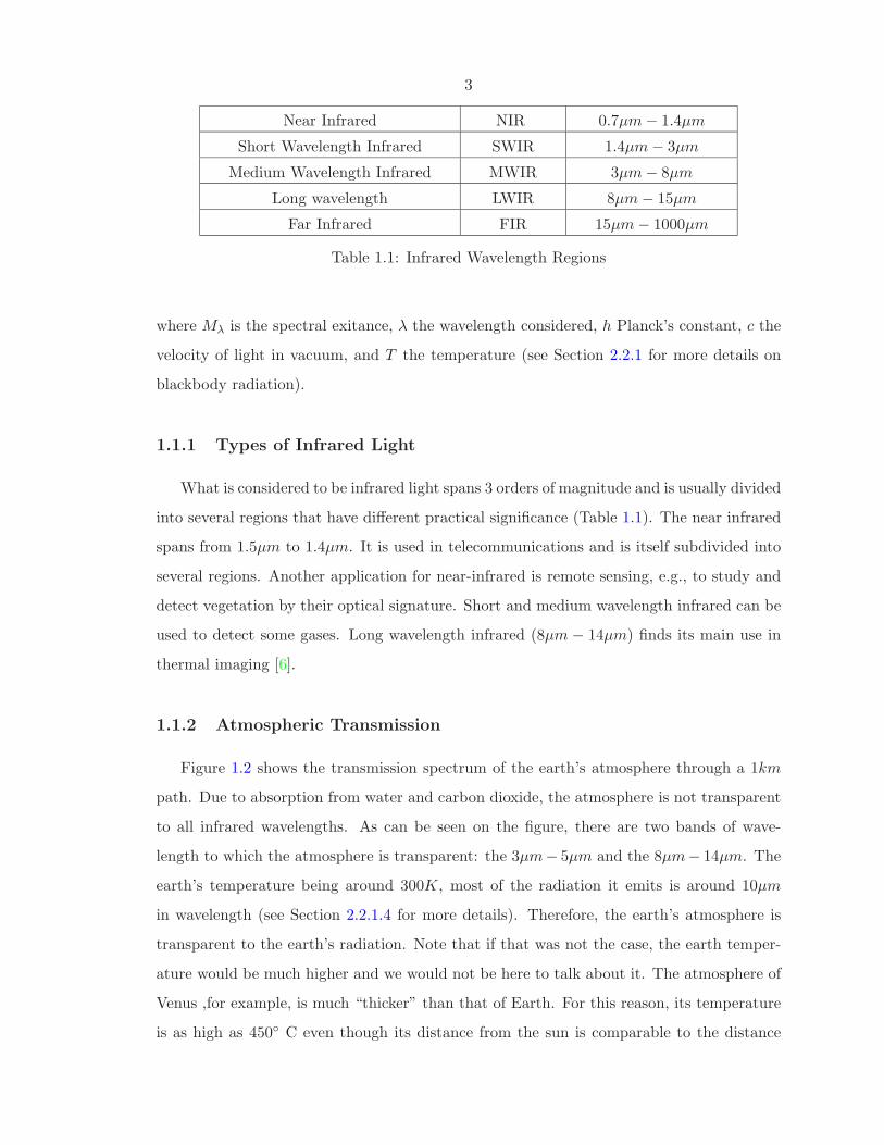
Table 1.1: Infrared Wavelength Regions
where Mλ is the spectral exitance, λ the wavelength considered, h Planck’s constant, c the
velocity of light in vacuum, and T the temperature (see Section 2.2.1 for more details on
blackbody radiation).
1.1.1 Types of Infrared Light
What is considered to be infrared light spans 3 orders of magnitude and is usually divided
into several regions that have different practical significance (Table 1.1). The near infrared
spans from 1.5µm to 1.4µm. It is used in telecommunications and is itself subdivided into
several regions. Another application for near-infrared is remote sensing, e.g., to study and
detect vegetation by their optical signature. Short and medium wavelength infrared can be
used to detect some gases. Long wavelength infrared (8µm − 14µm) finds its main use in
thermal imaging [6].
1.1.2 Atmospheric Transmission
Figure 1.2 shows the transmission spectrum of the earth’s atmosphere through a 1km
path. Due to absorption from water and carbon dioxide, the atmosphere is not transparent
to all infrared wavelengths. As can be seen on the figure, there are two bands of wave-
length to which the atmosphere is transparent: the 3µm− 5µm and the 8µm− 14µm. The
earth’s temperature being around 300K, most of the radiation it emits is around 10µm
in wavelength (see Section 2.2.1.4 for more details). Therefore, the earth’s atmosphere is
transparent to the earth’s radiation. Note that if that was not the case, the earth temper-
ature would be much higher and we would not be here to talk about it. The atmosphere of
Venus ,for example, is much “thicker” than that of Earth. For this reason, its temperature
is as high as 450 C even though its distance from the sun is comparable to the distance

4
co
2
h2
o
h2
o
h2
o
co
2
Figure 1.2: Atmosphere Transmission Spectrum
between the sun and the earth.
1.1.3 Remote Temperature Sensing and Thermal Imaging
For objects close to room temperature (300K), Wien’s displacement law (Equation 1.1)
predicts the wavelength of maximum blackbody emission around 10µm. From the Stefan-
Boltzmann law and Planck’s radiation law (Equation 1.2), the amount of infrared emitted
by a blackbody is a strong function of its temperature. Therefore, to remotely measured
the temperature of an object, one must be able to measure the amount of infrared radiation
it emits, preferably in the 8µm − 14µm atmospheric window. It is also possible to use the
3µm−5µm window, but less infrared is emitted in this range, making it more demanding on
the infrared detector that is used. Thermal imaging, which refers to the ability to measure
the temperature on different points on a scene, requires either an array of infrared detectors
operating in those wavelength ranges or a way to scan a scene using a single detector.
There are many applications to thermal imaging, civilian or military:
• Night vision
• Perimeter surveillance
• Vehicule/personnel detection
• Firefighting (smoke is transparent to LWIR)

5
• Industrial process monitoring
• Law enforcement
• Driver’s vision enhancement
• Public Health (e.g., detecting individuals with fever in airports)
Figure 1.3 shows some examples of thermal images obtained with commercial uncooled
thermal detector arrays.
1.2 Infrared Detectors
The different types of infrared detectors can be put in two categories: photon detectors
and thermal detectors.
1.2.1 Photon Detectors
Photon detectors directly convert incoming photons into photocurrents. The energy of
a photon having wavelength λ is
E =hc
λ
E(eV ) =1.24
λ(µm),
where c is the speed of light in vacuum and h is Planck’s constant. To detect infrared
radiation, photon detectors use phenomena that are activated by energies between ≃ 0.1eV
(for LWIR) to ≃ 1.8eV (for NIR).
Photodiodes In a photodiode, incoming photons are absorbed and generate electron-
hole pairs that are give rise to a photocurrent. For the photons to be absorbed by the
semiconductor, the bandgap of the semiconductor must be higher than the photons’ energy.
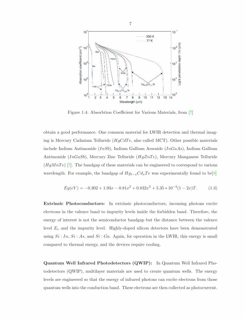
Figure 1.4 shows the absorption coefficient of several detector materials as a function of
wavelength. For a given material, the achievable photodiode signal-to-noise ratio depends
on the ratio αG , where α is the absorption coefficient and G the rate of thermal generation of
free charge carriers. In the LWIR range, i.e., the most suitable range for thermal imaging, it
is required to cool down the semiconductor to cryogenic temperatures (≤ 77K) in order to

6
(a) Preventive Maintenance/Process Monitoring (www.indigo.com)
(c) Night Vision on Combat Field (www.indigo.com)
(d) Perimeter Surveillance (www.ulis-ir.com)
Figure 1.3: Some Examples of Thermal Imaging Applications
7
Figure 1.4: Absorbtion Coefficient for Various Materials, from [7]
obtain a good performance. One common material for LWIR detection and thermal imag-
ing is Mercury Cadmium Telluride (HgCdTe, also called MCT). Other possible materials
include Indium Antimonide (InSb), Indium Gallium Arsenide (InGaAs), Indium Gallium
Antimonide (InGaSb), Mercury Zinc Telluride (HgZnTe), Mercury Manganese Telluride
(HgMnTe) [7]. The bandgap of these materials can be engineered to correspond to various
wavelength. For example, the bandgap of Hg1−xCdxTe was experimentally found to be[8]
Eg(eV ) = −0.302 + 1.93x − 0.81x2 + 0.832x3 + 5.35 ∗ 10−4(1 − 2x)T. (1.3)
Extrinsic Photoconductors: In extrinsic photoconductors, incoming photons excite
electrons in the valence band to impurity levels inside the forbidden band. Therefore, the
energy of interest is not the semiconductor bandgap but the distance between the valence
level Ev and the impurity level. Highly-doped silicon detectors have been demonstrated
using Si : In, Si : As, and Si : Ga. Again, for operation in the LWIR, this energy is small
compared to thermal energy, and the devices require cooling.
Quantum Well Infrared Photodetectors (QWIP): In Quantum Well Infrared Pho-
todetectors (QWIP), multilayer materials are used to create quantum wells. The energy
levels are engineered so that the energy of infrared photons can excite electrons from those
quantum wells into the conduction band. These electrons are then collected as photocurrent.

8
Similar to other photon detectors, QWIP need to be cooled. Even though the performance
of QWIP is not as good as MCT photodiodes, their uniformity and operability and yield
are higher. However, in cooled systems the cooling system accounts for a significant part of
the total cost [7].
1.2.2 Thermal Detectors
Although technically also “photon detectors”, thermal detectors are referred to this
way because they first convert photons into heat before measuring the induced change in
temperature. A thermal detector comprises an absorber which is thermally insulated to
give a big temperature change upon incoming radiation. Several physical mechanisms can
be used to measure this change in temperature. The main types of detection mechanisms
are briefly described below.
Gas Expansion: In 1936, Hammond Hayes published a paper entitled “A receiver of Ra-
diant Energy” in which he reported a new type of thermal detector[9]. He used pyrolyzed
flower pappus as a “fluff,” or gas absorber inside a closed chamber. When absorbing radi-
ation the gas inside the fluff expanded and would cause a chamber wall displacement. The
displacement was then measured capacitively, hence making device operable in Alternating
Current (AC) only. Based on the same idea of gas expansion, Harold Zahl and Marcel Golay
fabricated a “pneumatic infrared detector” published in 1946 [10]. Their device also used
the expansion of a gas due to heat temperature, but the way to detect the gas expansion
was through optical interference instead of an electrical signal. In 1947, Golay published
another paper presenting an improved version using light deflection from a flexible mirror
as a way to detect the gas expansion[11]. In a scanning configuration he demonstrated how
to display the “heat image” of an airplane in flight.2 Even though he was not the first to
use gas expansion as a way to detect infrared light, this type of infrared detector is known
as a “Golay Cell”. They are still commercially available today.
Thermopiles: In 1821, Thomas Seebeck discovered the thermoelectric effect and made
the first thermocouple. Seven years later, Leopoldo Nobili made the first “radiation thermo-
couple” using six antimony-bismuth thermocouples in series [12]. The electromotive force
2Which, to the author’s knowledge, is the first demonstration of thermal imaging.

9
appearing across a thermopile made of n thermocouples is given by
∆V = n
∫ T+∆T
TSa(T ) − Sb(T )dT
= ∆Tn(Sa − Sb) if Sa(T ) = Sa and Sb(T ) = Sb,
where Sa and Sb are the Seebeck coefficients of the two materials the thermocouples are
made of.
Pyroelectric Detectors: Pyroelectric detectors use pyroelectric materials to measure
the temperature change caused by infrared radiation. Pyroelectric materials are materials
that change polarization upon change in temperature. Pyroelectric detectors can only
operate in AC mode, as free charges will cancel the obtained polarization in DC. The
current flowing into or out of a pyroelectric detector made out of two electrode in between
which is a pyroelectric material, is given by [13]
I = ApdT
dt, (1.4)
where A is the area of the electrodes, p the pyroelectric coefficient, and dTdt the rate of
temperature change.
Thermomechanical Detectors: Thermomechanical infrared detectors use deflection of
composite cantilevers made of two materials having different coefficients of thermal ex-
pansion. This type of composite cantilever is called a bimetalic cantilever or a bimaterial
cantilever. They are (or were used) as low-cost temperature detectors in everyday applica-
tions, such as kitchen ovens or blinking Christmas decorations. The deflection at the tip of
the cantilever is given by [14]
∆z = C ∗ L3(α1 − α2)∆T, (1.5)
where C is a constant that depends on the materials’ thicknesses and their Young’s modulus,
L is the length of the cantilever, and α1 and α2 are the coefficients of thermal expansion of
the two layers. There are several ways this deflection can in turn be measured, e.g., optical
reading (deflection of a light beam on the cantilever), capacitive sensing ,or piezoresistive

10
sensing.
Bolometers: Bolometers are thermal sensors that use a thermistor to measure the tem-
perature change induced by incident infrared radiation. The change in bolometer resistance
due a change in temperature is given by
∆R = αR∆T, (1.6)
where α is the temperature coefficient of resistance of the thermistor and ∆T the temper-
ature change due to the incident radiation.
The theory and current state of the art of bolometers is described in detail in Chapter
2.
1.3 Micromachining for Uncooled Thermal Imaging
Since thermal detectors rely on a change of temperature induced by radiation, the
sensing element of a thermal sensor must be thermally insulated. Given the dimensions
achievable by conventional machining, this thermal insulation causes thermal detectors to
be much slower than photon detectors. Therefore during most of the twentieth century,
photon detectors were preferred to thermal detectors. However, as microelectronic fabrica-
tion techniques matured dramatically because of their use in integrated circuits, it became
possible to fabricate thermal detectors that were well thermally insulated and small enough
have an acceptable response time although, not comparable to that of photon detectors.
All types of uncooled thermal sensors discussed in the previous section have their micro-
machined version. Tunneling micro-Golay cells [15, 16], thermopile arrays [17, 18], thermo-
mechanical sensors, and arrays [19, 14] have been demonstrated. However, so far only two
technologies have found commercial success in uncooled thermal imagers: microbolometer
arrays and pyroelectric arrays.
In the 1980s the US Army Night Vision Laboratory (now part of the U.S. Army’s Night
Vision and Electronic Sensors Directorate, NVESD) and the Defense Advanced Research
Projects Agency (DARPA) funded microbolometer research at Honeywell International Inc.
[2]. The results of this research were declassified in 1992, revealing unexpectedly high un-
cooled microbolometer performance using vanadium oxide (VOx) as thermistor material.

11
Figure 1.5: Evolution of the Uncooled Infrared Industry in the US, from [20]
At about the same time, the Army Night Vision Laboratory and DARPA also sponsored
research on barium-strontium-titanate (BST) pyroelectric arrays developed at Texas In-
struments (now Raytheon Company). Texas Instruments Inc. also worked on bolometers
using amorphous silicon as the thermistor material. The Honeywell technology has since
been licensed to several companies. Figure 1.5 shows a schematic of the evolution of the
uncooled infrared detector array industry in the United States [20].

12
Bibliography
[1] W. Herschel, “Experiments on the refrangibility of the invisible rays of the sun,” Philo-
sophical Transactions of the Royal Society of London, vol. 90, pp. 284–293, 1800. Avail-
able on
http://www.jstor.org/. 1, 2
[2] R. Buser and M. Tompsett, “Historical overview,” in Semiconductor and Semimetals
(D. D. Skatrud and P. W. Kruse, eds.), vol. 47, ch. 1, Academic Press, 1997. 1, 10
[3] P. Kruse, L. McGlauchlin, and R. McQuistan, Elements of Infrared Technology: Gen-
eration, Transmission and Detection. John Wiley & Sons, Inc, 1962. 2
[4] “Aerospace science and technology dictionnary.”
http://www.hq.nasa.gov/office/hqlibrary/aerospacedictionary/. 2
[5] M. Planck, “On the law of distribution of energy in the normal spectrum,” Annalen
der Physik, vol. 4, 1901. 2
[6] “Infrared.” Wikipedia, 2005.
http://en.wikipedia.org/wiki/Infrared. 3
[7] A. Rogalski, “Infrared detectors: Status and trends,” Progress in Quantum Electronics,
vol. 27, no. 2, pp. 59–210, 2003. xi, 7, 8
[8] G. L. Hansen, J. L. Schmit, and T. N. Casselman, “Energy gap versus alloy composition
and temperature in hg1−xcdxte,” Journal of Applied Physics, vol. 53, no. 10, pp. 7099–
7101, 1982.
http://link.aip.org/link/?JAP/53/7099/1. 7
[9] H. V. Hayes, “A new receiver of radiant energy,” Review of Scientific Instruments,

13
vol. 7, no. 5, pp. 202–204, 1936.
http://link.aip.org/link/?RSI/7/202/1. 8
[10] H. A. Zahl and M. J. E. Golay, “Pneumatic heat detector,” Review of Scientific In-
struments, vol. 17, no. 11, pp. 511–515, 1946.
http://link.aip.org/link/?RSI/17/511/1. 8
[11] M. J. E. Golay, “A pneumatic infra-red detector,” Review of Scientific Instruments,
vol. 18, no. 5, pp. 357–362, 1947.
http://link.aip.org/link/?RSI/18/357/1. 8
[12] McGraw-Hill Encyclopedia of Science and Technology Online.
http://www.accessscience.com. 8
[13] P. Muralt, “Micromachined infrared detectors based on pyroelectric thin films,” Reports
on Progress in Physics, vol. 64, no. 10, pp. 1339–1388, 2001.
http://stacks.iop.org/0034-4885/64/1339. 9
[14] P. G. Datskos, N. V. Lavrik, and S. Rajic, “Performance of uncooled microcantilever
thermal detectors,” Review of Scientific Instruments, vol. 75, no. 4, pp. 1134–1148,
2004.
http://link.aip.org/link/?RSI/75/1134/1. 9, 10
[15] T. W. Kenny, W. J. Kaiser, S. B. Waltman, and J. K. Reynolds, “Novel infrared de-
tector based on a tunneling displacement transducer,” Applied Physics Letters, vol. 59,
no. 15, pp. 1820–1822, 1991.
http://link.aip.org/link/?APL/59/1820/1. 10
[16] T. Kenny, “Uncooled infrared imaging systems,” in Semiconductor and Semimetals
(D. D. Skatrud and P. W. Kruse, eds.), vol. 47, ch. 8, Academic Press, 1997. 10
[17] M. Foote, E. Jones, and T. Caillat, “Uncooled thermopile infrared detector linear
arrays with detectivity greater than 109cm.hz1/2w−1,” IEEE Transactions on Electron
Devices, vol. 45, September 1998. 10
[18] A. Schaufelbhl, N. Schneeberger, U. Mnch, M. Waelti, O. Paul, O. Brand, H. Baltes,
C. Menolfi, Q. Huang, E. Doering, and M. Loepfe, “Uncooled low-cost thermal imager

14
based on micromachined cmos integrated sensor array,” Journal Of Microelectrome-
chanical Systems, vol. 10, December 2001. 10
[19] Y. Zhao, M. Mao, R. Horowitz, A. Majumdar, J. Varesi, P. Norton, and J. Kitching,
“Optomechanical uncooled infrared imaging system: Design, microfabrication, and
performance,” Journal Of Microelectromechanical Systems, vol. 11, april 2002. 10
[20] J. Tissot, “Ir detection with uncooled focal plane arrays. state of the art and trends,”
Opto-Electronics Review, vol. 12, no. 1, p. 105109, 2004. xi, 11
15
Chapter 2
Uncooled Bolometers for ThermalImaging
Introduction
The Merriam-Webster dictionary entry for bolometer states:
Etymology: From the Greek bole, ray and metron, measure.
:A very sensitive thermometer whose electrical resistance varies with temper-
ature and which is used in the detection and measurement of feeble thermal
radiation and is especially adapted to the study of infrared spectra.
Although technically correct, this definition is incomplete because it does not explain how
the presence of radiation leads to a change in temperature and electrical resistance. A
more complete definition could be as follows: “A device that measures thermal radiation
by converting said radiation into a temperature change and subsequently measuring the
induced change in electrical resistance.”
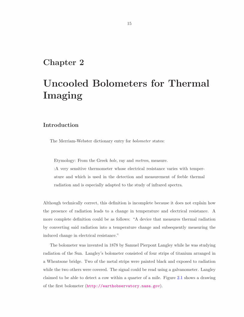
The bolometer was invented in 1878 by Samuel Pierpont Langley while he was studying
radiation of the Sun. Langley’s bolometer consisted of four strips of titanium arranged in
a Wheatsone bridge. Two of the metal strips were painted black and exposed to radiation
while the two others were covered. The signal could be read using a galvanometer. Langley
claimed to be able to detect a cow within a quarter of a mile. Figure 2.1 shows a drawing
of the first bolometer (http://earthobservatory.nasa.gov).

16
Figure 2.1: Langley’s Bolometer With its Optics.
2.1 Radiometry
To perform thermal imaging, we need to detect the thermal radiation coming from
an object and we need to know the relationship between the detected radiation and the
object temperature. Radiometry by definition is the science of radiation measurement.
This section introduces several important radiometry definitions. We then lay out the
equations governing the radiation exchange between a blackbody at a given temperature
and a detector through a lens.
2.1.1 Radiant Flux
The radiant flux φ(W ) emitted or received by a surface is the power of electromagnetic
radiation it emits or receives.
2.1.2 Irradiance
The irradiance E(W.m−2) of a surface is the amount of radiant flux it receives per unit
area.
2.1.3 Radiance
The radiance L(W.m−2.sr−1) of a surface is defined as the amount of radiant flux it
emits per unit of projected area and per unit of solid angle. This definition is better
understood if placed in the context of radiation exchanges between two surfaces. Let us
consider an infinitesimal element of area of a source dAs having radiance L emitting light
into a light cone dω. Let us call θs the angle between the surface dAs and the direction
of light propagation (Figure 2.2). Its projected , or foreshortened, area is defined as the

17
dAs cos θs
dAsdω
dω
Projected Area
θs
d2φ = L(θs)dAs cos θsdω
Figure 2.2: Concept of Radiance
projection of this area onto the plane which is normal to the direction of light propagation,
i.e., dAs cos θs. Let us now consider the light cone having an elemental solid angle dω
(Figure 2.2). Since the definition of radiance is the amount of radiant flux emitted by the
source per unit projected area and per unit of solid angle, the radiant flux emitted by dAs
in the light cone subtended by dω is
d2φ = L(θs)dAs cos θsdω. (2.1)
2.1.4 Exitance
The exitance M(W.m−2) of a surface is the total radiant flux it emits per unit area:
M ≡ dΦ
dAs=
∫
L(θs) cos θsdωd. (2.2)
The spectral exitance of a surface is the radiant flux it emits per unit area and per unit
wavelength:
Mλ ≡ dΦλ
dAs=
∫
Lλ(θs) cos θsdωd. (2.3)
where the integrals is taken over an hemisphere.
2.1.5 Intensity
Intensity I(W.sr−1) is the amount of radiant flux emitted per unit of solid angle:
I =dφ
dω(2.4)
= L(θs)dAs cos θs. (2.5)

18
θs
θd
r
dAs dAd
dωd
d2φ = L(θs)dAs cos θsdωd
dωd = dAd cos θd
r2
Figure 2.3: Radiation Exchange Between Two Infinitesimal Surfaces
2.1.6 Radiation Exchange Between Two Surfaces
Let us now consider the radiation exchange between a surface dAs and a detector surface
dAd, with r the distance between the two surfaces, θs and θd the angle between the light
propagation direction and the surface dAs and dAd, respectively (Figure 2.3).
As seen before from the definition of radiance we have
d2Φ = L(θs)dAs cos θsdωd, (2.6)
with dωd the solid angle subtended by dAd from dAs. Using the definitions in Figure 2.3
this can also be written
d2Φ = L(θs)dAsdAd cos θs cos θd
r2(2.7)
and
d2Φ = L(θs)dAd cos θddωs, (2.8)
with dωs the solid angle subtended by dAs from dAd.
2.1.7 Lambertian Surfaces
By definition, the radiance of a Lambertian surface L(θs) is independent of θs:
L(θs) = L. (2.9)
Let us consider an elemental Lambertian surface dAs located in the center of a receiving
hemisphere of radius r. By definition, the exitance M of the surface dAs is the total amount
of radiant flux emitted per unit of area. In the following the subscript letter, h represents
the hemisphere. Because the source is in the center of the hemisphere, we have θh = 0 for
19
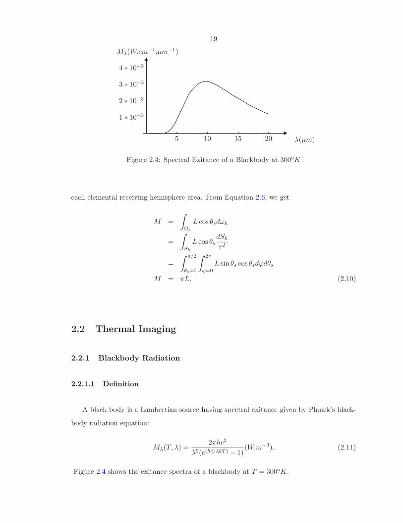
λ(µm)
Mλ(W.cm−1.µm−1)
1 ∗ 10−3
2 ∗ 10−3
3 ∗ 10−3
4 ∗ 10−3
5 10 15 20
Figure 2.4: Spectral Exitance of a Blackbody at 300oK
each elemental receiving hemisphere area. From Equation 2.6, we get
M =
∫
Ωh
L cos θsdωh
=
∫
Sh
L cos θsdSh
r2
=
∫ π/2
θs=0
∫ 2π
ϕ=0L sin θs cos θsdϕdθs
M = πL. (2.10)
2.2 Thermal Imaging
2.2.1 Blackbody Radiation
2.2.1.1 Definition
A black body is a Lambertian source having spectral exitance given by Planck’s black-
body radiation equation:
Mλ(T, λ) =2πhc2
λ5(e(hc/λkT ) − 1)(W.m−3). (2.11)
Figure 2.4 shows the exitance spectra of a blackbody at T = 300oK.

20
Material Emissivity
Aluminum foil 0.04
Steel (polished) 0.07
Brick 0.93
Glass 0.95
Human skin 0.98
Water 0.96
Wood 0.9
Concrete 0.95
Table 2.1: Emissivity of Various Materials
2.2.1.2 Radiance
From Equation 2.10 the spectral radiance is simply
Lλ(T, λ) =M(T, λ)
π(W.m−3.sr−1). (2.12)
Real materials always have an exitance smaller than the ideal blackbody, given by
Lλ(T, λ) = ǫλM(T, λ)
π(W.m−3.sr−1), (2.13)
where ǫλ < 1 is the material spectral emissivity. Materials for which the spectral emissivity
is independent of the wavelength (i.e., ǫλ = ǫ) are called graybodies. Although these are only
hypothetical since no material emits at all wavelengths of the electromagnetic spectrum,
some materials have spectral emissivities that can be considered constant across wavelengths
of practical interest (e.g., LWIR). Table 2.1 shows the emissivities of various materials.
2.2.1.3 Exitance
The total exitance of a blackbody is given by the Stefan-Boltzmann’s law:
M(T ) =
∫ +∞
0Mλ(T, λ)dλ = σbT
4, (2.14)
where σb = 5.607 ∗ 10−8W.m−2K−4 is the Stefan-Boltzmann constant.

21
2.2.1.4 Wien’s Displacement Law
The wavelength of maximum spectral excitance λmax of a blackbody depends on its
temperature T . From Equation 2.11, λmax and T can be shown to satisfy the relation
λmaxT =hc
5k(1 − exp−hc
kλmaxT ), (2.15)
which can be solved numerically to give
λmaxT = 2.8978 ∗ 10−3(m.K),
or in a more convenient form
λmax(µm) =2897.8
T (K). (2.16)
Therefore, objects close to room temperature (T ∼ 300oK) radiate mostly at wavelengths
within the 8µm − 14µm atmospheric window (LWIR).
2.2.2 Radiation Transfer Between an Object and a Detector
To remotely measure the temperature of an object or a scene one must collect the
radiation it emits on a detector. In this section, we derive the expression of the irradiance
on a detector Ed due to an object having a spectral exitance Mλ,o when the radiation coming
from the object is focused on the detector using a lens of focal length f and of diameter D.
Figure 2.5 shows the typical imaging system configuration. f is the focal distance of the
lens , zo is the distance between the object and the lens, and zi is the distance between the
image (or detector) and the lens.
First we calculate the spectral radiant flux Φλ,o→l being transferred from the object
surface Ao to the lens surface Al. Assuming the there are no losses in the lens, this spectral
radiant flux will then be incident on the detector surface Ad. Figure 2.6 shows the geometry
definitions used for this calculation.
From Equation 2.1 we get
Φλ,o→l(T, λ) =
∫
Ao
∫
Ωl
Lλ,o(T, λ) cos θdωldAo

22
θiθ0
zizo
D2
Lens
Object Image
Figure 2.5: Typical Imager
= AoLλ,o(T, λ)
∫
Ωl
cos θdωl,
where dωl is the elemental solid angle.
From Figure 2.6, we make the appropriate substitutions
θ = θl,
dωl =dAl
r2cos θ,
r =zo
cos θ,
r′ = zo tan θ,
dAl = r′dϕdr′
=z2o tan θ
cos2 θdϕdθ,
dωl = sin θdϕdθ,
Φλ o→l(T, λ) = AoLλ,o(T, λ)
∫ 2π
0
∫ θ0
0sin θ cos θdθdϕ
= AoπLλ,o(T, λ) sin2 θ0. (2.17)
For or a Lambertian object we can substitute Equation 2.10 into Equation 2.17 to get
Φλ,o→l(T, λ) = AoMλ,o(T, λ) sin2 θ0. (2.18)
From Abbe’s sine condition (also called the optical sine theorem)[1] we have
Ad sin2 θi = Ao sin2 θo.

23
Ao
θl
θθ0
ϕ
D2
r′
rz0
Al
Lens
Figure 2.6: Imaging System Geometry Definitions
Therefore, the spectral radiant flux incident on the detector is
Φλ,o→d(T, λ) = AdMλ,o(T, λ) sin2 θi
= AdMλ,o(T, λ)NA2
Φλ,o→d(T, λ) =AdMλ,o(T, λ)
4F 2, (2.19)
and the irradiance on the detector surface is
Eλ,d(T, λ) ≡ Φλ,o→d(T, λ)
Ad
=Mλ,o(T, λ)
4F 2, (2.20)
where
NA ≡ sin θi (Numerical Aperture) (2.21)
F ≡ 1
2NA=
1
2 sin θi(F-Number). (2.22)
Equation 2.19 is well know among photographers (in fact it is also called the camera equa-
tion) because it relates the irradiance on a photographic film to the scene radiance and

24
camera F-number. For an object located at infinity (z0 = f) and if f ≫ D, we have
F =1
D
√
D2
4+ f2
≃ f
D.
In the literature, the focal ratio f/D and F are often considered to be identical and are
simply referred to as “the F-number” or “f/#”. However, this approximation leads to
significant errors when F is comparable to 1.
2.2.3 Radiation Transfer Between a Blackbody and a Detector
If a blackbody at temperature T radiates to a detector having an area Ad through an
optical system having F-number F , the radiant flux on the detector in the [λ1 − λ2] band
is given by integrating Equation 2.19
Φ[λ1,λ2](T ) =
∫ λ2
λ1
Φλ(T, λ)dλ
=Ad
4F 2
∫ λ2
λ1
M(λ, T )dλ
=Ad
4F 2
∫ λ2
λ1
2πhc2
λ5(e(hc/λkT ) − 1)dλ. (2.23)
2.3 Bolometer Theory
2.3.1 Electrical-Thermal Analogy
To study the behavior of thermal systems in general and bolometers in particular, it
is very convenient to use the electro-thermal analogy. To find the thermal equivalent of
electrical quantities, we start by noting that in electronics one studies the behavior and
motion of electrons, i.e., electric charge. In thermal engineering we are interested in the
behavior of thermal energy instead. Therefore, the first step in building the electro-thermal
analogy is stating that electric charge and thermal energy are equivalent:
q(C) ⇔ E(J)
Charge ⇔ Thermal Energy

25
Electric current is the amount of charge that passes through a section per unit of time. The
thermal equivalent is then energy per unit of time, i.e., power:
I =dq
dt(A) ⇔ P =
dE
dt(W )
Electric Current ⇔ Thermal Power.
The reason why electric charge flows from one region in space to another region in space is
the presence of a potential gradient (electric field). Equivalently, the reason why thermal
energy flows from one region in space to another region in space is the presence of a temper-
ature gradient. Therefore, the thermal equivalent of electrostatic potential is temperature:
V (V ) ⇔ T (K)
Electric Potential ⇔ Temperature.
Using the same kind of reasoning, one can easily find the thermal equivalents of other
electrical quantities such as current density, conductivity, conductance, and capacitance.
J =dI
dS(A.m−2) ⇔ Q =
dP
dS(W.m−2)
Current Density ⇔ Thermal Energy Flux,
J = −σ∇V (A.m−2) ⇔ Q = −κ∇T (W.m−2)
Electrical Conduction ⇔ Thermal Conduction,
σ(A.V −1.m−1) ⇔ κ(W.K−1.m−1)
Electrical Conductivity ⇔ Thermal Conductivity,
G =L
σWt⇔ Gth =
L
κWt
Electrical Conductance ⇔ Thermal Conductance,
I = CdV
dt⇔ P = Cth
dT
dt
Electrical Capacity ⇔ Thermal Capacity, and
C[C.V −1] ⇔ Cth[J.K−1]
Electrical Capacitance ⇔ Heat Capacity.

26
Current Bias Ib
Absorber
Incident Radiation Φ
Temperature T0 + ΦGth
Heat Capacity Cth
Absorptivity η
Thermal Conductance Gleg
Heat Sink (substrate)
Temperature T0
Thermistor
Resistance R(T )
TCR α
Figure 2.7: Bolometer Principle
2.3.2 Structure
Figure 2.7 shows a simplified bolometer structure. An absorber is linked to a heat sink
through a low thermal conductance Gleg. As it absorbs an incident radiant flux Φ(W ), the
temperature increases. By measuring the resistance of a thermistor placed on the absorber,
one can calculate the amount of absorbed radiant flux.
2.3.3 Model
Using the electrical-thermal analogy introduced in Section 2.3.1, we can draw the elec-
trical equivalent of the bolometer thermal circuit, which is a classical first-order, RC-type
circuit (Figure 2.8). The losses through radiation are modeled with a thermal conductance
Grad. The expression of Grad is found by taking the derivative of the total exitance of
a blackbody around room temperature (Equation 2.14) and multiplying by the bolometer
area 2 ∗ Ad (because both the top surface and the bottom surface of the bolometer are
radiating):
Grad = 2AddησT 4
dT= 8AdσT 3. (2.24)

27
T0
ηΦT
Rleg = 1/Gleg
Rrad = 1/Grad
Cth
Universe
Figure 2.8: Bolometer Equivalent Electric Circuit
The total thermal conductance Gth is given by
Gth = Gleg + Grad. (2.25)
The radiation conductance is often neglected, however it should be noted that if the thermal
conductance to the substrate Gleg approaches the value of the radiation conductance Grad,
then both should be taken into account.
2.3.3.1 Static Behavior
In steady state, we have
T (Φ) = T0 +ηΦ
Gth
∆T (Φ) ≡ T (Φ) − T0.
Therefore, if the thermistor has a resistance R0 at room temperature and a Temperature
Coefficient of Resistance (TCR) α, we have
R(Φ) = R0(1 + α∆T (Φ))
= R0(1 + αηΦ
Gth)
∆R(Φ) = R0αηΦ
Gth,

28
and the voltage signal ∆V measured when biasing the bolometer with a current Ib is 1
∆V (Φ) = IbR0αηΦ
Gth. (2.26)
Equation 2.26 leads to the definition of the voltage responsivity ℜ:
ℜ(V.m−1) ≡ ∆V (Φ)
Φ=
αηR0Ib
Gth. (2.27)
As one would naturally expect from Figure 2.7, ℜ is high when:
1. The absorptivity is high (most of the incoming radiant flux is absorbed and converted
to temperature rise).
2. The thermal conductance is small (good absorber insulation, high temperature rise
for a given absorbed radiant flux).
3. The TCR of the thermistor is big (big change in thermistor resistance for a given
change in absorber temperature).
4. Ib is high (big change in signal voltage for a given change in thermistor resistance).
2.3.3.2 Dynamic Behavior
Let us define
Φ(jω) ≡ Φ0(ω)ejωt (2.28)
and
∆T (jω) ≡ ∆TΦ0(ω)ej(ωt+ϕ). (2.29)
We can write the expression of the thermal transfer function (which, using the electrothermal
analogy of Section 2.3.1 is equivalent to a complex impedance):
Hth(jω) ≡ ∆T (jω)
ηΦ(jω)=
1
Gth(1 + jωτth). (2.30)
1We assume for now that the temperature of the absorber is not affected by the Joulean heating resultingfrom Ib.

29
Bolometer
Integrator
Vb
Figure 2.9: Simple Bolometer Readout Circuit
It follows that
∆T (ω) =ηΦ0
Gth
√
1 + (ωτth)2,
where τth, the thermal time constant of the bolometer, is given by
τth ≡ Cth
Gth. (2.31)
From Equation 2.31, it is obvious that there is a trade-off between D.C. responsivity and
thermal time constant. In fact, if one wants to increase ℜ by decreasing Gth while keeping
τth unchanged, Cth has to be decreased by the same amount as Gth.
2.3.4 Signal Readout
Figure 2.3.4 shows a simplified bolometer readout circuit in a voltage bias configuration.
Typically, a voltage pulse is applied for a duration τpulse, and the resulting current is
integrated. The result of the integration is multiplied by the appropriate coefficient to
give a value of the average bolometer current. The power dissipated by Joulean heating
during readout will cause a temperature increase on the bolometer. Because the thermal
conductivity from bolometer to substrate is low by design, this temperature rise might be
significant. If we assume that the α remains constant during the readout, the temperature
∆T (t) must satisfy
R(∆T )Ib2 = Cth
∆T
dt+ Gth∆T,
R0(1 + α∆T )Ib2 = Cth
∆T
dt+ Gth∆T,

30
and using ∆T (jω) as defined in Equation 2.29
∆T (jω) =R0Ib
2
(Gth − R0αIb2) + jCthω
=R0Ib
2
Geff + jCthω
=R0Ib
2
Geff
1
1 + jωτeff, (2.32)
with
Geff = Gth − R0αIb2 (2.33)
τeff =Cth
Geff=
Cth
Gth − R0αIb2 . (2.34)
Equations 2.33 and 2.34 show that the bolometer temperature still exhibits a first-order
frequency response. However, depending on the sign of α, the effective thermal constant
can be greater or lower than the intrinsic thermal conductance. The effective time constant
will be lower or greater, respectively. This is due to the fact that for a constant current,
the power injected in the bolometer varies:
∆T (t) =R0Ib
2
Geff
(
1 − exp(− t
τeff))
. (2.35)
Equations 2.33 and 2.34 show that if α is positive (as would be the case for a metallic
thermistor), there exists a critical biasing current Icrit for which Geff and τeff will become
negative:
Icrit =
√
Gth
R0α. (2.36)
If Ib > Icrit, the bolometer will experience thermal runaway, as Equation 2.35 clearly shows.
Such runaway is very likely to destroy or damage the bolometer.2
For t ≪ τeff we have, from Equation 2.35,
∆T (t) ≃ R0Ib2
Geff
t
τeff
≃ R0Ib2
Cth(2.37)
Therefore, if τpulse ≪ τeff , the temperature ∆Tτpulseat the end of the integration pulse of
2However, we assumed that α was independent of T , which might not be true, especially at high temper-atures.
31
length τpulse is
∆Tpulse =R0I
2b τpulse
Cth. (2.38)
Equation 2.38 shows that even if α is negative and/or thermal runaway is avoided, the
integration time τpulse and bias current Ib must be chosen so that the temperature increase
∆Tpulse is low enough to avoid damaging the bolometer. Finally, as will be shown in Section
2.3.5, τpulse will affect the bolometer noise performance.
2.3.5 Noise
There are several uncorrelated sources to bolometer noise: the Johnson noise (or thermal
noise), the 1/f noise (also called flicker noise), and the background noise. The 1/f noise
depends on the material used and on the geometry of the device. In this section, we
discuss these different noise contributions in the case of the timed-integration readout circuit
discussed in Section 2.3.4.
2.3.5.1 Readout Circuit Noise Bandwidth
The total noise at the output of a circuit having transfer function H(f) and input power
noise spectral density Si(f) is given by
< Vn2 > =
∫ +∞
0So(f)df
= Si
∫ +∞
0|H(f)|2df
= SiB, (2.39)
where B is the noise bandwidth defined by
B ≡∫ +∞
0|H(f)|2df.

32
The readout circuit described in Section 2.3.4 averages the signal over an integration time
τpulse. Its impulse response h(t) is
h(t) =
0 for t < 0
1τpulse
for 0 ≤ t ≤ τpulse
0 for t > τpulse
and its transfer function H(f) is
H(f) = e−jπfτpulsesinπfτpulse
πfτpulse. (2.40)
The noise bandwidth of the readout circuit can be calculated by integrating Equation 2.40,
but it is easier to calculate it using Parseval’s relation:
B =
∫ +∞
0
(sinπfτpulse
πfτpulse
)2df
=1
2
∫ +∞
−∞
|H(f)|2df
=1
2
∫ +∞
−∞
h(t)2dt
=1
2
∫ τpulse
0
1
τpulse2dt
B =1
2τpulse. (2.41)
2.3.5.2 Johnson Noise
Due to its resistive nature, the bolometer exhibits Johnson (thermal) Noise . J.B.
Johnson experimentally found that the noise power spectral density in a resistor of resistance
R0 given by [2]
Sj = 4kTR0. (2.42)
where k is the boltzmann constant and R0 is the electrical resistance of the bolometer at
room temperature. Equation 2.42 was proven theoretically by Harry Nyquist[3].3
When the bolometer signal is read by the integrated and dump circuit presented in Sec-
tion 2.3.4, the Johnson noise at the output is found by combining Equation 2.42, Equation
3In fact, Nyquist’s paper appear right after Johnson’s in the same issue of the same journal [2, 3].
33
2.39, and Equation 2.41:√
< Vj2 > =
√
2kTR0
τpulse. (2.43)
We conclude this section on Johnson noise by showing that the Johnson noise voltage can
be expressed as a function of the temperature rise the bolometer experiences during the
readout/integration pulse (see Section 2.3.4). Substituting Equation 2.38 into Equation
2.43 gives√
< Vj2 > = Vb
√
2kT
∆TpulseCth. (2.44)
This important result shows that to minimize the Johnson noise contribution to the total
bolometer noise it is desirable to use materials that can handle a high temperature increase
during readout.
2.3.5.3 1/f Noise
While measuring noise in vacuum tubes, Johnson found that not only was there a white
noise (the thermal noise discussed above) but also another noise component which was
stronger at low frequencies, which he failed to explain [4]. This noise is called 1/f noise, or
flicker noise, and is found in many physical systems, electrical and others[5].
The 1/f noise (or flicker noise) power spectral density of a resistor is given by
Sf (f) =KV b
b
fa(2.45)
where Vb is the bias voltage across the resistor, K is a constant that depends on the material
used as well as on the geometry of the resistor, a is a constant that depends on the material
and which is usually found to be close to 1, and b is a constant that is usually found to be
between 0.5 and 2 [6]. In many cases, the 1/f noise is equal to (or approximated by)
Sf (f) =KV 2
b
f. (2.46)
Despite what is believed by some, no resistor is free of 1/f noise. However, the magnitude
of this noise depends on the resistor material and geometry.

34
In a famous paper published in 1969 [7], F.N. Hooge proposed a “universal” relation
K =αH
nV, (2.47)
where n is the charge carrier density of the material, V is the total volume of the resistor,
and αH is an empirical constant depending on the resistor material. Some measurements of
αH are collected in [8]. It should be noted that if 1/f noise actually follows Equation 2.47,
then for a material with fixed sheet resistance (i.e., fixed thickness and fixed resistivity) a
“small” square will have less noise than a “big” square, even though their Johnson noise will
be identical. Such a volume dependence was reported for VOx (vanadium oxide) films and
p-nc-SiC:H films in [9] and [10] respectively. However, little literature is available regarding
1/f noise in materials, and authors often cite values for K in materials without mentioning
the volume of the resistors considered.
We want to calculate the total noise in a pulsed-bias bolometer with integration time
τpulse. In many publications this noise power is calculated using the equation
< Vf2 > =
∫ B
f1
Sf (f)df,
leading to a noise power
< Vf2 > = KV 2
b lnB
f1= KV 2
b ln1
2f1τpulse. (2.48)
where B is the noise bandwidth and f1 is an arbitrary frequency chosen to avoid the
divergence of Sf at f = 0. However, Equation 2.48 is incorrect and is due to a common
misunderstanding of the definition of noise bandwidth. It is true that the total thermal
noise is given by
< Vj2 > =
∫ B
0Sj(f)df, (2.49)
but only because Sj(f) = Sj . When a noise power spectral density depends on frequency,
the concept of noise bandwidth cannot be used. The correct expression for the 1/f noise

35
power at the output of the integrating readout circuit is
< Vf2 > =
∫ +∞
f1
|H(f)|2 KVb2
fdf
=
∫ +∞
f1
(sinπfτpulse
πfτpulse
)2 KVb2
fdf
= KVb2
∫ +∞
πf1τpulse
sin2 x
x3dx.
We define Ja,b as
Ja,b =
∫ b
a
sin2 x
x3dx
=
∫ b
a
1 − cos 2x
2x3dx
=[cos 2x − 1
4x2
]b
a+
1
2
∫ b
a
sin 2x
x2dx
=[cos 2x − 1
4x2
]b
a−
[sin 2x
2x
]b
a+
∫ b
a
cos 2x
xdx
=[cos 2x − 1
4x2
]b
a−
[sin 2x
2x
]b
a+
∫ 2b
2a
cos u
udu
=[cos 2x − 1
4x2
]b
a−
[sin 2x
2x
]b
a+ Ci(2b) − Ci(2a)
=cos 2b − 1
4b2− cos 2a − 1
4a2− sin 2b
2b+
sin 2a
2a+ Ci(2b) − Ci(2a),
where Ci(x) is the cosine integral defined by
Ci(x) ≡ −∫ +∞
x
cos u
udu. (2.50)
then
< Vf2 > = KVb
2
∫ +∞
πf1τpulse
sin2 x
x3dx
= KVb2Jπf1τpulse,+∞
< Vf2 > = KVb
2(1 − cos 2πf1τpulse
4(πf1τpulse)2+
sin 2πf1τpulse
2πf1τpulse− Ci(2πf1τpulse)
)
. (2.51)
Equation 2.51 can be simplified using the fact that in most cases 2πf1τpulse ≪ 1.
The first-order series expansion of Ci(x) is [11]
Ci(x) = γ + ln(x) + O(x)2, (2.52)
36
where γ = 0.58 is the Euler-Mascheroni constant. Therefore, the first-order series expansion
of < Vf2 > is
< Vf2 >= KVb
2(3
2− γ − ln(2πf1τpulse) + O(2πf1τpulse)
2)
. (2.53)
Equation 2.53 shows that Equation 2.48 overerestimates the 1/f noise power by
−KVb2(
3
2− γ − lnπ) ≃ 0.22KVb
2.
2.3.5.4 Temperature Fluctuation Noise and Background Noise
An abbreviated and adapted derivation of thermal fluctuation noise and background
noise based on the more general case in [12] is given below. The mean-square fluctuations
in energy of a system with thermal capacity Cth is
< ∆E2 > = kT 2Cth. (2.54)
This random fluctuation of the energy stored in the bolometer will induce a random fluc-
tuation in bolometer temperature, which in turn will lead to a random fluctuation of the
bolometer voltage, i.e., a temperature fluctuation voltage noise.
The bolometer temperature and its stored energy are linked through
∆E = Cth∆T (2.55)
From Equation 2.54 and Equation 2.55, the mean-square temperature fluctuation is found
to be
< ∆TTF2 >=
< ∆E2 >
Cth2 =
kT 2
Cth. (2.56)
Let us assume that this temperature fluctuation is due to a fluctuation in radiant flux ΦTF
and that the power spectral density SΦTFof ΦTF is independent of frequency. We can write
SΦTF(f) = S0.
Therefore,
< ∆TTF2 >=
∫ +∞
0S0η
2|Hth(j2πf)|2df,

37
where Hth is the thermal transfer function defined in Equation 2.30:
< ∆TTF2 > =
S0η2
Gth2
∫ +∞
0
1
1 + (2πfτth)2df
< ∆TTF2 > =
S0η2
4GthCth. (2.57)
Combining Equation 2.56 and Equation 2.57, we get
S0 =4kT 2Gth
η2. (2.58)
Using the ∆V = αVb∆T , the power spectral density of the temperature fluctuation voltage
noise can be written
STF (f) = α2Vb2S0η
2|Hth(j2πf)|2 =4kT 2α2Vb
2
Gth
1
1 + (2πfτth)2. (2.59)
However, if the frequencies of interest are much higher than 1/2πτth, the total voltage noise
can be approximated by
√
< VTF2 > = αVb
√
kT 2
Cth(2.60)
(which can also be found using Equation 2.56).
As noted in [12], if most of the heat loss from the bolometer is due to radiation, Gth
reduces to the radiation thermal conductivity Grad = 8ηAdσbT3 and the temperature fluc-
tuation noise identifies with the background noise, i.e., the noise due to fluctuations in the
rate of arrival of photons on the bolometer.
2.3.6 Noise-Equivalent Power
The noise equivalent power (NEP) of a bolometer is defined as the amount of radiant
flux incoming on the bolometer that would lead to a voltage signal equivalent to the noise
power:
NEP ≡ Vn
ℜ =
√
V 2j + V 2
f + V 2TF
ℜ . (2.61)

38
2.3.7 Detectivity
The detectivity D∗, sometimes called “D star”, is a figure of merit that normalizes
performance to the square root of area and bandwidth.
D∗ ≡ ℜ√
BAd
Vn, (2.62)
where A is the area of the detector and B is the bandwidth of the bolometer/readout
system. The bandwidth of the measurement should also be taken into account because for
any noise power spectral density one could theoretically reduce the total noise by reducing
the bandwidth (e.g., by using an integrator with an arbitrarily long integration time).
However, as noted in [13], detectivity is not a good figure of merit for thermal detectors
(such as bolometers) or thermal imagers. The detectivity was originally defined for photon
detectors. The reason for taking the area Ad into account in the detectivity is the fact that
in such detectors the dominating noise power (usually generation-recombination noise) is
proportional to the detector area. This is not the case for thermal detectors. In fact, if
one assumes that Hooge’s formula for 1/f noise holds (Equation 2.47), the noise power is
inversely proportional to the area (for constant thickness).
Some authors use the following alternative definition:
D∗′ ≡ ℜ√
Ad
Sn, (2.63)
where Sn is the total noise power spectral density. If bolometer noise is dominated by
Johnson noise or temperature fluctuation noise, then Vn =√
SnB and the two definitions
are equivalent. However when 1/f noise is non-negligible, using the alternative definition
overestimates the bolometer performance.
2.3.8 Noise Equivalent Temperature Difference
The most relevant figure of merit for bolometers used for thermal imaging is the Noise-
Equivalent Temperature Difference (NETD). It is the smallest temperature change on a
target that one can measure using said bolometer. Quantitatively, the NETD is defined as
the temperature difference on a blackbody target that will lead to a signal-to-noise ratio of
1.

39
To calculate the NETD of a bolometer, we start by calculating the change in radiant
flux the bolometer will receive when the target temperature changes. The change in radiant
flux falling on the detector per oK change on the source is found by differentiating Equation
2.23:
dΦλ1−λ2
dT(W.K−1) =
∫ λ2
λ1
dΦλ(T, λ)
dTdλ
=Ad
4F 2
∫ λ2
λ1
M(λ, T )
dTdλ
=Ad
4F 2
∫ λ2
λ1
M(λ, T )hce(hc/λkT )
kλT 2(e(hc/λkT )−1)dλ
=Ad
4F 2
(dM
dT
)
T,[λ1,λ2],
where(dM
dT
)
T,[λ1−λ2]=
∫ λ2
λ1
M(λ, T )hce(hc/λkT
kλT 2(e(hc/λkT )−1)dλ. (2.64)
If we define Vs(∆Ttarget) to be the signal voltage caused by a temperature difference ∆Ttarget,
the NETD is
NETD =∆Ttarget
Vs(∆Ttarget)/Vn
=∆TtargetVn
ℜ∆TtargetdΦλ1−λ2
dT
=4F 2∆TtargetVn
Adℜ∆Ttarget
(
dMdT
)
T,[λ1−λ2]
NETD =4F 2Vn
Adℜ(
dMdT
)
T,[λ1−λ2]
. (2.65)
From Equation 2.61, we can write the NETD as a function of the NEP:
NETD = NEP4F 2
Ad
(
dMdT
)
T,[λ1−λ2]
, (2.66)
or using Equation 2.62, as a function of the detectivity D∗:
NETD =
√B ∗ 4F 2
D∗√
Ad
(
dMdT
)
T,[λ1−λ2]
. (2.67)

40
1
1.5
2
3
5
Gleg(W.K−1)
NETDTF (mK)
10−11 10−10 10−9 10−8 10−7 10−6
Figure 2.10: Ideal NETD as a Function of Gleg, adapted from [12]
2.3.9 Theoretical Limitations
Even if one could measure a temperature in a way that was free of Johnson noise and
1/f noise, the temperature-fluctuation would still be present:
NEPTF =√
S0B
=
√
4kT 2GthB
η2, (2.68)
where S0 is defined in Equation 2.58 and B is the bandwidth considered. From Equation
2.66, the expression of the temperature fluctuation-limited NETD is
NETDTF =4F 2NEPTF
Ad
(
DMdT
)
T,[λ1−λ2]
=8F 2T
√kGthB
ηAd
(
dMdT
)
T,[λ1−λ2]
. (2.69)
Equation 2.69 shows the temperature fluctuation-limited NETD for a bolometer at temper-
ature T irradiated by a blackbody source at the same temperature.
To reduce this NETD, the most obvious way is to reduce the thermal conductance Gleg
in order to reduce the total thermal conductance Gth. However, once the total thermal
conductance reaches Grad, further reduction of Gleg does not improve the NETD and the

41
bolometer reaches its background temperature fluctuation noise limit[12]. The NETD is
then given by
NETDBG =8F 2T
√
k8ησbT 3AdB
ηAd
(
dMdT
)
T,[λ1−λ2]
(2.70)
=16F 2
√
2kσbT 5B√
ηAd
(
dMdT
)
T,[λ1−λ2]
. (2.71)
As discussed in Section 2.4.1, for thermal imaging applications the area Ad cannot be
changed dramatically. For an array used at video frame rate (30Hz), the integration time
τpulse has to be 33ms or less. Figure 2.10 shows the minimum achievable NETD as a
function of the suspension thermal conductance Gleg for τpulse = 33ms, η = 1, F = 1,
Ad = 50µm ∗ 50µm, T = 300K, λ1 = 8µm, and λ2 = 14µm.
2.4 State of the Art
2.4.1 Orders of Magnitude
2.4.1.1 Pixel Size
When designing a LWIR imager, it is desirable to minimize the pixel size (as long as
one is able to obtain the desired thermal conductance). There are two reasons for that: the
cost of the optics and spatial resolution. The optical materials used for LWIR optics such
as Germanium (Ge), Zinc Selenide (ZnSe), and Zinc Sulfide (ZnS) are expensive (in part
because they require anti-reflection coating). It is therefore desirable to reduce the diameter
of the lens used. For a constant F number, this requires a smaller array and therefore a
smaller pixel size. A smaller pixel array is desirable to achieve high spatial resolution while
keeping a reasonable size for the array. The theoretical minimum pixel size is dictated by
the diffraction limit (assuming a perfect lens). The diameter of the first Airy disc is given
by
d =f
D2.44λ. (2.72)
thus for LWIR infrared and for an F/1 optics (typical for uncooled bolometer imaging ar-
rays), this leads to a minimum pixel size of about 30µm. However, for such a pixel size it
would be difficult to achieve high fill-factor and low thermal conductance with available mi-

42
λ(µm)
Mλ(W.cm−2.µm−1)
T1 = 293K
T2 = 306K∆M ≃ ∆T
(
dMdT
)
T,8µm−14µm
1 ∗ 10−3
2 ∗ 10−3
3 ∗ 10−3
4 ∗ 10−3
3 8 145 10 20
Figure 2.11: Spectral Exitance of Blackbody Sources at Different Temperatures
crofabrication techniques and materials. The typical pixel size in state-of-the-art bolometer
arrays is between 35µm and 50µm.
2.4.1.2 Bolometer Temperature Resolution
Suppose we want to use a bolometer array to “see” a person with a skin temperature of
33oC (≃ 360oK) in a room at 20oC (≃ 293oK). Figure 2.11 shows the difference of spectral
exitance in the wavelength range considered. The difference in exitance (shaded on Figure
2.11) between the background and the subject over the 8µm−14µm range can be estimated
to be:
∆M ≃ ∆Ts
(dM
dT
)
300K,8µm−14µm. (2.73)
From Equation 2.64 we calculate
(dM
dT
)
300K,8µm−14µm= 2.6 ∗ 10−4W.cm−2. (2.74)
For a change ∆Ts in source temperature, the difference in radiant flux incoming on the
bolometer is given by
∆Φ =Ad∆Ts
4F 2
(dM
dT
)
300K,8µm−14µm, (2.75)

43
and the corresponding change in bolometer temperature is given by
∆Td =Ad∆Ts
4GthF 2
(dM
dT
)
300K,8µm−14µm. (2.76)
Let us consider a bolometer and its optical system having parameters F = 1, Ad = (50µm)2,
and Gth = 10−7W.K−1 and calculate the changes in incoming radiant flux (Equation 2.75)
and bolometer temperature (Equation 2.76) for different changes in source temperature.
• If ∆Ts = 13oC (difference between human subject skin and background at room
temperature), we have ∆Φ = 21.1nW and ∆Td = 211mK.
• If ∆Ts = 50mK,we have ∆Φ = 81.2pW and ∆Td = 812µK. Hence, by definition, to
have an NETD of 50mK the resolution of the bolometer temperature measurement
needs to be better than 812µK.
2.4.2 Vanadium Oxide (VOx) Bolometers
Vanadium oxide bolometers are one of the most successful kinds of bolometers. They
combine high TCR (≃ 2%.K−1) and low 1/f noise. Table 2.2 shows a summary of param-
eters for a 240*336 array. The achieved NETD is 39mK.
2.4.3 Titanium Bolometers
Titanium has been demonstrated as a thermistor material in bolometers [15, 16]. One of
the main advantages of using titanium is its full compatibility with IC fabrication processes,
allowing monolithic integration. Although titanium has a relatively low TCR (compared
with other bolometer materials), its low 1/f leads to an acceptable performance (see dis-
cussion in Section 2.5.4).
2.4.4 Silicon Bolometers
Amorphous silicon is used in commercial bolometer arrays in the US by Raytheon Com-
pany and in France by ULIS. Amorphous silicon has the advantage of being easily integrated
into IC fabrication processes while having a good TCR. However, the 1/f is high as well.
The NETD claimed by Raytheon (now Thermal-Eye) in its handheld 160∗120 pixel cameras
is 100mK [17]. The ULIS UL01011 is said to have an average NETD of 85mK [18].

44
Parameter Value
Pitch 50µm
Fill Factor 70%
Support material 0.8µm Silicon Nitride
Beam Lateral Dimensions 2µm ∗ 50µm
Thermal Capacitance 3 ∗ 10−9J.K−1
Thermal Conductance 2 ∗ 10−7W.K−1
Thermal Time Constant 15ms
Absorptivity 80%
Sensing Material Vanadium Oxide
TCR −2.3%.K−1
Pixel Resistance 20kΩ
Responsivity 3.2 105V.W−1@Vb = 5V
Detector Noise 20µV
Frame Rate 30Hz
Integration Time 5µs
Bias Current 250µA
NETD (F/1) 39mK
Table 2.2: Parameters of a 240*336 Array of VOx Bolometers, from [14]

45
Parameter Value
Pitch 50µm
Fill Factor 59%
Support material 0.8µm CVD Silicon Dioxide
Absorptivity unreported
Thermal Conductance 2.2 ∗ 10−7W.K−1
Thermal Time Constant 15ms
Absorptivity 80%
Sensing Material Titanium
TCR +0.25%.K−1
Pixel Resistance 3.4kΩ
Responsivity 1.06 105V.W−1 ∗ η@Vb = 8.5V
Frame Rate 30Hz
Integration Time 5.3µs
Bias Current 2.50mA
NETD (F/1) 90mK
Table 2.3: Parameters of a 128*128 Array of Titanium Bolometers, from [15]

46
In [19], Eminoglu et. al. reported single-crystal silicon bolometers fabricated using
a CMOS post-processing. Again, the integration with IC fabrication is a very attractive
feature. However, the obtained TCR is low (.34%.K−1). Because the 1/f is very small
in single-crystal silicon, the noise is dominated by Johnson noise. The obtained NETD of
80µm ∗ 80µm pixels with F/1 optics and using a 125µs integration time was 470mK.
2.4.5 Other Types of Bolometers
Among other materials used to fabricate bolometers are Yttrium Barium Copper Oxide
(YBaCuO) [20, 21]. High TCRs can be achieved while the 1/f noise remains relatively
low. In [22], Hayashi et. al. use Perovskite Manganese Oxide (BiLaSrMnO) as the sensi-
tive material. The reported NETD is lower than 100mK (although the noise itself is not
reported). olycrystalline silicon germanium alloys (Poly SiGe) were reported in [23] with an
achieved TCR of 2%.K−1 and a 1/f noise factor of K = 6.62 ∗ 10−12. A bolometer based
on amorphous germanium-silicon-oxygen (GeSiO) was presented in [24]. The reported TCR
is high but is obtained for high values of resistivities (105Ω.cm). The achieved responsivity
was 380V.W−1, but the value of 1/f noise was not reported. silicon carbide was also pro-
posed as the temperature sensitive material in [25]. The TCR was reported to be as high
as 6.5%.K−1. However, even though the 1/f noise spectral was measured, the bias and the
frequency at which the measurement was made were not reported.
2.5 Reaching the Theoretical Limit
If the total bolometer noise is dominated by the temperature fluctuation noise, the
theoretical limit is reached and the NEP and NETD can only by reduced by decreasing
Gth.4 In this section, we discuss 1/f noise and Johnson noise only. The 1/f noise-limited
NETD and the Johnson noise-limited NETD are given respectively by
NETDf =4F 2Gth
Adηα(
dMdT
)
T,[λ1−λ2]
√
K(3
2− γ − ln(2πf1τpulse)
)
(2.77)
NETDj =4F 2Gth
AdηαVb
(
dMdT
)
T,[λ1−λ2]
√
2kTR
τpulse(2.78)
4For a given area.

47
2.5.1 Lower Gth and Cth
The pixel-to-substrate thermal conductance of current bolometers is about three times
higher than their radiative thermal conductance. Progress could still be made by decreasing
the pixel-to-substrate conductance. However, the thermal time constant of most state-of-
the-art bolometers is on the order of a few tens of milliseconds, the maximum acceptable
for thermal imaging. As mentioned in Section 2.3.3.2, any lowering of thermal conductance
would have to be accompanied by a lowering of thermal capacitance. Most existing devices
use metallic or semiconducting thermistors and metallic electrodes; these materials can not
be made freestanding without a supporting material which adds dead thermal conductance
and dead thermal capacitance to the device. It would be desirable to find a materials which
could be used as electrode and/or thermistor without the need of a supporting material.
2.5.2 Higher Absorptivity
Most current bolometers rely on quarter-wavelength cavities to reach absorptivities η
close to 80% in the 8µm−14µm band. Therefore, only little could be gained from increasing
the absorptivity.
2.5.3 Wider Bandwidth
One could think of using materials with absorptivities high enough to not require cavi-
ties. The 3µm− 5µm band could then be used in conjunction with the 8µm− 14µm band.
However, the NETD would only by marginally improved because the of the low exitance of
blackbody sources in this band, as shown in Equation 2.79 and Equation 2.80.
(dM
dT
)
300K,[3µm−5µm]= 2.1 ∗ 10−5W.cm−2.K−1 (2.79)
(dM
dT
)
300K,[8µm−14µm]= 2.6 ∗ 10−4W.cm−2.K−1 (2.80)
2.5.4 Higher TCR and Lower 1/f Noise Material
Having a material with higher TCR α would improve both responsivity and NETD.
There are indeed materials with TCRs higher than those found in current bolometers.
Unfortunately, it often comes at the price of higher resistivity (therefore more Johnson
noise) and higher 1/f noise. Usually, increasing the TCR by half of an order of magnitude

48
leads to an increase in resistivity and 1/f noise by several orders of magnitude. It is
important to note that in terms of NETD, the TCR is not the only parameter to consider.
The total noise of a bolometer biased at Vb during an integration time τpulse is given by
(2.3.5):√
KV 2b
(3
2− γ − ln(2πf1τpulse)
)
+2kTR
τpulse. (2.81)
If we define a constant
C =4F 2
Ad
(
dMdT
)
T,[λ1−λ2]
,
then combining Equation 2.81 and Equation 2.65 we get:
NETD =
CGth
√
KV 2b
(
32 − γ − ln(2πf1τpulse)
)
+ 2kTRτpulse
ηαVb. (2.82)
As can be seen on Equation 2.82, if the total noise is dominated by the Johnson noise
(second term in the square root), an increase in Vb or τpulse results in a better NETD.
Then, if all other parameters are constant, the NETD reduces to
NETDf =
CGth
√
K(
32 − γ − ln(2πf1τpulse)2
)
ηα. (2.83)
Equation 2.83 suggests the introduction of a figure of merit β for materials to be used as the
temperature sensor in bolometers (such a figure of merit was originaly proposed in [26]):
β =|α|√K
. (2.84)
For VOx having a TCR of −2.3%.K−1, the 1/f noise constant is reported to be K = 10−13
[14]. This leads to a value β = 7.3 ∗ 104K−1.V.Hz−1/2. For films of titanium having
a TCR of 0.25%.K−1, the reported 1/f noise constant is K = 3 ∗ 10−15, leading to a
β = 4.6 ∗ 104K−1.V.Hz−1/2. Therefore, even though the TCR of titanium is one order of
magnitude lower than that of VOx, the 1/f noise-limited NETD that can be obtained with
Ti is only 2.4 times higher than what can be obtained with VOx. Vanadium oxide and
titanium are currently used in bolometer arrays precisely because they have a good ratio of
TCR over noise. However, one can hope for materials that would surpass the existing ones

49
in terms of β which would reduce the 1/f -limited NETD.
2.5.5 Integration Time and Current Bias
Both the 1/f noise and the Johnson noise are decreasing functions of the integration
time.5 Figure 2.12 shows the Johnson and 1/f noise contributions for different values of
bolometer resistance and 1/f noise factor KVb2. It appears that if the 1/f noise is dominant,
increasing the integration time has very little effect on the total noise. For example if a
bolometer has a resistance R0 = 20kΩ and a 1/f noise factor KVb2 = 10−13 V 2, then
• For an integration time τpulse = 1µs, the noise is dominated by Johnson noise and is
about 10µV .
• For an integration time τpulse = 100µs, the contribution of Johnson noise and 1/f
noise are comparable and total noise approaches 1µV .
• For an integration time τpulse = 10ms, the noise is dominated by 1/f noise and is
virtually the same as it was for τpulse = 100µs.
If the noise is Johnson-dominated, it can be reduced by increasing the integration time or by
increasing the biasing current. Once the contributions of Johnson noise and 1/f noise are
comparable, it is useless to further increase the integration time or to the further increase
the biasing current.
5For realistic numbers design parameter f1 << 1
τpulseand Equation 2.83 is defined.

50
10−2
10−3
10−3
10−4
10−4
10−5
10−5
10−6
10−6
10−7
10−7
1/f Noise for KVb2 = 10−11 V 2
1/f Noise for KVb2 = 10−12 V 2
1/f Noise for KVb2 = 10−13 V 2
Johnson Noise for R = 200Ω
Johnson Noise for R = 20KΩ
Johnson Noise for R = 2MΩ
Vol
tage
Noi
se(V
)
Integration Time τpulse(s)
Figure 2.12: Noise Behavior for Different Integration Times

51
Bibliography
[1] M. Bass, ed., Handbook of Optics, vol. II: Devices, Measurements, & Properties.
McGraw-Hill, 2d ed., 1995. 22
[2] J. Johnson, “Thermal agitation of electricity in conductors,” Phys. Rev., vol. 32, 1928.
32
[3] H. Nyquist, “Thermal agitation of electric charge in conductors,” Phys. Rev., vol. 32,
1928. 32
[4] J. Johnson, “The schottky effect in low frequency circuits,” Phys. Rev., vol. 26, p. 7185,
1925. 33
[5] E. Milotti, “1/f noise: a pedagogical review,” tech. rep., 2001.
http://arxiv.org/ftp/physics/papers/0204/0204033.pdf. 33
[6] P. Gray, P. Hurst, S. Lewis, and R. Meyer, Analysis and Design of Analog Integrated
Circuits. John Wiley and Sons, Inc, 4 ed., 2001. 33
[7] F. N. Hooge, “1/f noise is no surface effect,” Phys. Lett., vol. 29A, 1969. 34
[8] F. Hooge, “1/f noise sources,” IEEE Transactions on Electron Devices, vol. 41, no. 11,
pp. 1926–1935, 1994. 34
[9] V. Y. Zerov, Y. V. Kulikov, V. Malyarov, I. Kherbtov, I. Shaganov, , and E. Shadrin,
“Vanadium oxide films with improved characteristics for ir microbolometeric matrices,”
Technical Physical Letters, vol. 27, pp. 378–380, 2001. 34
[10] H. K. Lee, S. Y. Myong, K. S. Lim, and E. Yoon, “Electrical properties of photo-
cvd boron-doped hydrogenated nanocrystalline silicon-carbide (p-nc-sic:h) films for un-
cooled ir bolometer applications,” Journal of Non-Crystalline Solids, vol. 316, pp. 297–
301, 2003. 34

52
[11] E. W. Weisstein, “Cosine integral.,” MathWorld–A Wolfram Web Resource, 2005.
http://mathworld.wolfram.com/CosineIntegral.html. 35
[12] P. W. Kruse, Uncooled Thermal Imaging. Arrays, Systems, and Applications. SPIE-
The International Society for Optical Engineering, 2001. xi, 36, 37, 40, 41
[13] P. G. Datskos and N. V. Lavrik, “Detectors figures of merit,” tech. rep., Oak Ridge
National Laboratory, 2003. 38
[14] R. A. Wood, “Uncooled infrared imaging systems,” in Semiconductor and Semimetals
(D. D. Skatrud and P. W. Kruse, eds.), vol. 47, ch. 3, Academic Press, 1997. xiv, 44,
48
[15] A. Tanaka, S. Matsumoto, N. Tsukamoto, S. Itoh, K. Chiba, T. Endoh, A. Nakazato,
K. Okuyama, Y. Kumazawa, M. Hijikawa, H. Gotoh, T. Tanaka, and N. Teranishi,
“Infrared focal plane array incorporating silicon ic process compatible bolometer,”
IEEE Transactions on Electron Devices, vol. 46, no. 11, 1996. xiv, 43, 45
[16] H. Lee, J. Yoon, E. Yoon, S. Ju, Y. Yong, W. Lee, and S. Kim, “A high fill-factor
infrared bolometer using micromachined multilevel electrothermal structures,” IEEE
Transactions on Electron Devices, vol. 46, pp. 1489–1491, July 1999. 43
[17] “Thermal-eye x100xp brochure,” tech. rep., Thermal-Eye, 2005. 43
[18] “Ul 01011 brochure,” tech. rep., ULSI-IR, 2004. 43
[19] S. Eminoglu, D. Tezcan, M. Tanrikulu, and T. Akin, “Low-cost uncooled infrared
detectors in cmos process,” Sensors and Actuators A, vol. 109, 2003. 46
[20] A. Jahanzeb, C. Travers, Z. Celik-Butler, D. Butler, and S. Tan, “A semiconduc-
tor ybacuo microbolometer for room temperature ir imaging,” IEEE Transactions On
Electron Devices, vol. 44, pp. 1795–1801, October 1997. 46
[21] M. Almasri, D. Butler, and Z. Celik-Butler, “Self-supporting uncooled infrared mi-
crobolometers with low-thermal mass,” Journal of Microelectromechanical Systems,
vol. 10, pp. 469–476, September 2001. 46

53
[22] K. Hayashi, E. Ohta, H. Wada, H. Higuma, and S. Miyashita, “Fabrication of bilasrmno
uncooled microbolometer,” Japanese Journal of Applied Physics, vol. 1, pp. 5281–5284,
March 2001. 46
[23] S. Sedky, P. Fiorini, M. Caymaxa, C. Baert, L. Hermans, and R. Mertens, “Char-
acterization of bolometers based on polycrystalline silicon germanium alloys,” IEEE
Electron Device Letters, vol. 19, October 1998. 46
[24] E. Iborra, M. Clement, L. V. Herrero, and J. Sangrador, “Ir uncooled bolometers based
on amorphous gexsi1−xoy on silicon micromachined structures,” Journal of Microelec-
tromechanical Systems, vol. 11, August 2002. 46
[25] T. Ichihara, Y. Watabe, Y. Honda, and K. Aizawa, “A high performance amorphous
sic:h thermistor bolometerbased on micro-machined structure,” in International Con-
ference on Solid-state Sensors and Actuators Transducers 97, (Chicago, IL), june 1997.
46
[26] P. C. Shan, Z. Celik-Butler, D. P. Butler, A. Jahanzeb, C. M. Travers, W. Kula,
and R. Sobolewski, “Investigation of semiconducting ybacuo thin films: A new room
temperature bolometer,” Journal of Applied Physics, vol. 80, no. 12, pp. 7118–7123,
1996. 48

54
Chapter 3
Pyrolyzed Parylene as a MEMSMaterial
3.1 Parylene
3.1.1 Chemical Structure and Deposition Process
Parylene is a generic name for poly-para-xylylene (parylene N) and its modified ver-
sions, parylene C and D [1]. Figure 3.1 shows the chemical structure of different types of
commercially available parylenes. Parylene is a polymer deposited by vapor phase. Figure
3.2 shows the deposition process for parylene C. A powder of di-monochloro-para-xylylene
dimer (Figure 3.3) is placed into a vaporizer taken to temperatures up to 170C. The
dimer sublimates and enters a pyrolysis section at 690C where it is broken into para-
monochloro-xylylene monomer. The monomer vapor then enters the deposition chamber,
which is normally at room temperature. The monomer vapor then polymerizes into poly-
para-monochloro-xylylene on surfaces inside the chamber. In a typical parylene deposition
system, the pressure inside the chamber is regulated by controlling the vaporizer tempera-
ture through a feedback loop. The film quality is a function of the pressure. If the pressure
is too high, the quality of the parylene film will be poor[2]. Typical vapor pressures are
n
CH2CH
2
Parylene N
CH
n
2
Cl
CH2
Parylene C
Cl
Cl
CH2
CH2
Parylene D
n
Figure 3.1: Chemical structure of different types of parylenes

55
CH2
CH22
Cl
CH2
CH2
Cl
CH2
CH2
Cl
CH
n
2
Cl
CH2
Cold Trap, −70C
2:Pyrolysis, 690C
1:Sublimation, 170C
Vacuum Pump
3:Deposition, 23C, 22mTorr
di-para-monochloro-xylylene
para-monochloro-xylylene
poly-monochloro-para-xylylene
Figure 3.2: Parylene Deposition Process
Figure 3.3: Di-para-xylylene Dimer
between 10mTorr and 100mTorr, leading to deposition rates of about 0.7µm per hour
for parylene N and 5µm for parylene C and D. Because parylene molecules bounce many
times before depositing and polymerizing, parylene films are highly conformal. Pinhole-free
parylene films as thin a a few hundred angstroms can be deposited. The deposition rate
of parylene has a strong dependence on substrate temperature (increasing with decreasing
temperature). For this reason the cold trap located before the pump is highly effective in
capturing the excess vapor before it reaches the pump. On the other hand, the deposition
rate can be greatly reduced by increasing the substrate temperature and is negligible if the
substrate temperature is above 140C. Using this fact, localized substrate heating can be
used to selectively deposit parylene on certain substrate areas [3, 4].
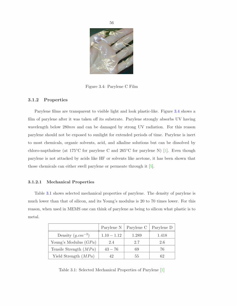
56
Figure 3.4: Parylene C Film
3.1.2 Properties
Parylene films are transparent to visible light and look plastic-like. Figure 3.4 shows a
film of parylene after it was taken off its substrate. Parylene strongly absorbs UV having
wavelength below 280nm and can be damaged by strong UV radiation. For this reason
parylene should not be exposed to sunlight for extended periods of time. Parylene is inert
to most chemicals, organic solvents, acid, and alkaline solutions but can be dissolved by
chloro-napthalene (at 175C for parylene C and 265C for parylene N) [1]. Even though
parylene is not attacked by acids like HF or solvents like acetone, it has been shown that
those chemicals can either swell parylene or permeate through it [5].
3.1.2.1 Mechanical Properties
Table 3.1 shows selected mechanical properties of parylene. The density of parylene is
much lower than that of silicon, and its Young’s modulus is 20 to 70 times lower. For this
reason, when used in MEMS one can think of parylene as being to silicon what plastic is to
metal.
Parylene N Parylene C Parylene D
Density (g.cm−3) 1.10 − 1.12 1.289 1.418
Young’s Modulus (GPa) 2.4 2.7 2.6
Tensile Strength (MPa) 43 − 76 69 76
Yield Strength (MPa) 42 55 62
Table 3.1: Selected Mechanical Properties of Parylene [1]

57
3.1.2.2 Electrical Properties
Table 3.2 shows electrical properties of parylene. Parylene is a good electrical insulator;
in fact, it has been studied as a possible low-k dielectric in integrated circuits [6]. The
dielectric dissipation factor is one of the parameters that varies the most among the dif-
ferent types of parylene. Electrostatic actuators made of free-standing parylene have been
demonstrated, e.g., in [7]. However, it has also been shown that under high electric field,
parylene surfaces undergo charging [8].
Parylene N Parylene C Parylene D
Volume Resistivity (Ω.cm) 1.4 ∗ 1017 8.8 ∗ 1016 1.2 ∗ 1017
Dielectric Strength (V.cm−1) 2.76 ∗ 106 2.21 ∗ 106 2.17 ∗ 106
Dielectric Constant @60Hz 2.65 3.15 2.84
Dissipation factor @60Hz 2 ∗ 10−4 4 ∗ 10−2 4 ∗ 10−3
Table 3.2: Selected Electrical Properties of Parylene [1]
3.1.2.3 Thermal Properties
Table 3.3 shows selected thermal properties of parylene. As can be seen, the thermal
conductivity of parylene is extremely low, about four orders of magnitude lower than metals
and silicon and more than one order of magnitude lower than silicon dioxide and silicon
nitride. In fact, the thermal conductivity of parylene C (which is lowest among parylenes) is
only three times that of air. The thermal capacity per unit volume is also a few times lower
than metals, silicon, oxide, or nitride. The melting point is different among the different
types of parylene. Parylene N has the highest melting point at 420C, and parylene C has
the lowest melting point at 290C. The coefficient of thermal expansion of parylene is one
order of magnitude higher than that of silicon and of the same order of magnitude as metals.
3.1.3 Parylene as a MEMS Material
Over the past decade, parylene has become more and more popular among researchers
in the Micro Electro-Mechnanical Systems (MEMS) field. Parylene can easily be patterned
using conventional lithography and O2 etching. Furthermore its low-temperature deposi-

58
Parameter Parylene N Parylene C Parylene D
Melting Point ( C) 420 290 380
Linear Coefficient of Expansion (K−1) 6.9 ∗ 10−5 3.5 ∗ 10−5 3 − 8 ∗ 10−5
Thermal Conductivity (W.m−1.K−1) 0.13 8.4 ∗ 10−2 −Specific Heat (J.K−1.g−1) 0.84 0.71 −
Volumic Heat Capacity (J.K−1.cm−3) 0.92 0.92 −
Table 3.3: Selected Thermal Properties of Parylene [1]
tion, conformality, and biocompatibility make it an attractive candidate for devices such as
microfluidic and implantable devices [9, 10].
3.2 Parylene Pyrolysis
3.2.1 Pyrolysis
Pyrolysis, from the Greek pyro (fire) and lusis (loosen) is defined as the decomposition
of a material or compound due to heat [11]. For organic materials, pyrolysis has to be
performed in the absence of oxygen to avoid oxidation. For this reason it is sometimes
called “incomplete combustion”.
Pyrolysis has been known and used for centuries, even though it is impossible to say
how many. In fact, it is interesting to know that it was by pyrolysis of organic materials
that Thomas Edison produced his first incandescent filaments. He stated in his patent on
“Electric Lamp” awarded in 1880 [12]:
“I have discovered that even a cotton thread carbonized and placed in a glass
bulb exhausted to one millionth of an atmosphere offers from one hundred to
five hundred ohms resistance to the passage of current.”
Reports of phenol formaldehyde resin (bakelite) pyrolysis can be traced back to the
1960s [13], and other polymers such as polyimide have also been studied [14]. Mechanical
properties of carbon films obtained by pyrolysis of furfuryl alcohol-modified phenolic resin
were reported in [15].
In [16, 17] the potential of pyrolyzed photoresist for MEMS and electrochemical ap-
plications was investigated. Table 3.4 shows the sheet resistance of 6µm films of AZ4330

59
Pyrolysis Temperature Sheet Resistance (Ω/¤)
600 146.4
700 845.8
800 244.8
900 94.3
1000 57.1
1100 52.1
Table 3.4: Sheet Resistance of 6µm films of Photoresist after Pyrolysis, after [17]
photoresist pyrolyzed at different temperatures from [17]. The minimum obtained resistiv-
ity was 5.1 ∗ 10−3Ω.cm, which is comparable to commercial glassy carbon. The measured
weight loss was up to 69% and the thickness shrinkage up to 84%. It was also reported that
films obtained by pyrolysis at 600C had an unstable resistivity.
In [18], Wang et al. proposed using free-standing pyrolyzed-photoresist as tunable resis-
tors. They found that by using different biasing currents the resistance of the free-standing
resistors could be increased or decreased. Their conclusion was that the increase of re-
sistance was due to thermal oxidation (the experiments were made in air) and that the
decrease in resistance was due to further carbonization. Another prior work of interest was
conducted by Hui et al. [19]. In this work parylene was pyrolyzed above 700C in order to
produce a high-temperature sacrificial layer that could be easily removed by oxidation at
high temperature. However, the transition of properties from parylene to carbon was not
reported, and neither were mechanical and electrical properties. Two attractive features
of parylene are first the fact that it is free of any solvent or of any feature-enhancer (as
opposed to photoresist or polyimide) and second that its chemical vapor deposition process
of parylene leads to very pure films. Therefore, it is reasonable to think that pyrolysis of
parylene films leads to carbon films of better quality and having a better reproducibility.
In the following sections, we report for the first time on the properties of parylene C films
after pyrolysis. We present data on the structure and mechanical and electrical properties
of parylene films after pyrolysis at temperatures ranging from 400C to 1500C. We also
discuss some of the issues associated with the integration of pyrolyzed-parylene films into
regular MEMS fabrication processes in order to use those films in devices.

60
3.2.2 Process
4µm-thick parylene C films were deposited on silicon wafers and pyrolyzed at different
temperatures in N2 atmosphere with a 10C/min ramp rate. In addition to silicon, parylene
films were deposited on silicon/titanium/platinum (Si/Ti/Pt) and silicon/chrome/gold to
estimate catalytic effects of platinum and gold.
3.2.2.1 Appearance and Thickness Change
Under an optical microscope, pyrolyzed-parylene films look dark, smooth, and contin-
uous. No changes in lateral directions of parylene C film could be observed in our experi-
ments. The thicknesses of parylene films were measured before and after pyrolysis with an
Alphastep surface profilometer. Figure 3.5 shows the thickness (%) as the ratio of thickness
between the pyrolyzed films and their initial thickness. Only little changes in thickness can
be observed for temperatures below 500C. In fact, there is little change in the appearance
of the films as well. Films pyrolyzed at 600C on Si experienced a shrinkage of about 75%,
while films pyrolyzed at 800C and above experienced a shrinkage of about 80%. Shrinkage
appears to continue to occur as the pyrolysis temperature is increased above 800C, but
only slightly. The thickness of films pyrolyzed on Si/Ti/Pt decreased by 85% for 800C
pyrolysis, while that of films pyrolyzed Si and Si/Cr/Au decreased by 80% for 800C py-
rolysis. This indicates a slight catalytic effect of platinum on the pyrolysis process and no
catalytic effect of gold.
3.2.2.2 Weight Loss
The weight of several parylene C films were measured before and after pyrolysis. Figure
3.6 shows the weight (in %) of pyrolyzed films where 100% is their initial weight. As
expected (and similar to thickness change), very little weight change occurs for pyrolysis
temperatures below 500C. It was found that after exposure to air (20C, 47% in humidity)
the weight of pyrolyzed-parylene film decreases if baked at 100C or if placed in vacuum.
The weight then increases when once exposed to air. We believe this weight change is due
to moisture absorption and desorption. Electrical resistivity experiments also suggest that
pyrolyzed-parylene films can absorb airborne moisture (See Section 3.2.5.4). As can be seen
on Figure 3.6, the weight loss of films pyrolyzed on silicon/titanium/platinum is about 5%

61
0
Film on Si
Film on Si/Cr/Au
Film on Si/Ti/Pt
0
Thic
knes
sC
han
ge(%
)
Pyrolysis Temperature(C)
20
40
60
80
100
200 400 600 800 1000
Figure 3.5: Thickness Change
higher than that of films pyrolyzed on bare silicon or silicon/chrome/gold. However, there
is no observable shift in the temperature at which the weight loss starts to occur.
3.2.2.3 TEM
A film of parylene C pyrolyzed at 800C was observed using a Transmission Electron
Microscope (TEM) (Figure 3.7), and small amounts of graphite-like crystallite structures
can be seen. The electron-diffraction diagram also confirms the existence of (002) plane of
graphite. However, as a whole, this film is recognized as amorphous carbon.
3.2.2.4 TGA, DSC, and Raman Analysis
Thermogravimetric analysis (TGA) and differential scanning calorimetry (DSC) was
performed in the solid state ionics and electroceramics lab at the California Institute of
Technology 1 and reported in [20]. Thermogravimetric analysis (TGA )and differential
scanning calorimetry (DSC) were performed simultaneously on a film of parylene C. Figure
3.9 reproduces the obtained data. As seen in Figure 3.9, the material undergoes an en-
dothermic phase transition at 296C [20]. This is consistent with the melting temperature
1data taken by graduate student Stacey Boland

62
20
40
60
80
Film on SiFilm on Si/Cr/AuFilm on Si/Ti/Pt
Wei
ght
Los
s(%
)
Pyrolysis Temperature(C)
2000
0
100
400 600 800 1000
Figure 3.6: Weight Loss
Lattice Structure
Amorphous Structure
10nm10nm
Figure 3.7: Pyrolyzed Parylene TEM Micrograph
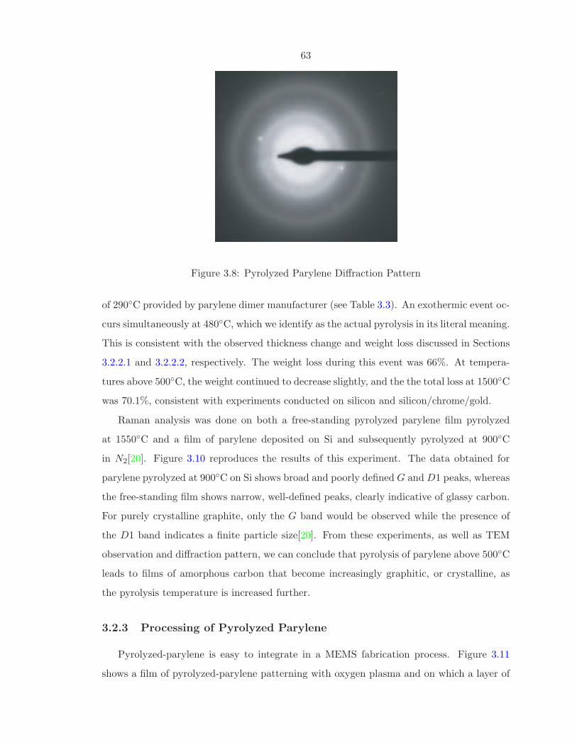
63
Figure 3.8: Pyrolyzed Parylene Diffraction Pattern
of 290C provided by parylene dimer manufacturer (see Table 3.3). An exothermic event oc-
curs simultaneously at 480C, which we identify as the actual pyrolysis in its literal meaning.
This is consistent with the observed thickness change and weight loss discussed in Sections
3.2.2.1 and 3.2.2.2, respectively. The weight loss during this event was 66%. At tempera-
tures above 500C, the weight continued to decrease slightly, and the the total loss at 1500C
was 70.1%, consistent with experiments conducted on silicon and silicon/chrome/gold.
Raman analysis was done on both a free-standing pyrolyzed parylene film pyrolyzed
at 1550C and a film of parylene deposited on Si and subsequently pyrolyzed at 900C
in N2[20]. Figure 3.10 reproduces the results of this experiment. The data obtained for
parylene pyrolyzed at 900C on Si shows broad and poorly defined G and D1 peaks, whereas
the free-standing film shows narrow, well-defined peaks, clearly indicative of glassy carbon.
For purely crystalline graphite, only the G band would be observed while the presence of
the D1 band indicates a finite particle size[20]. From these experiments, as well as TEM
observation and diffraction pattern, we can conclude that pyrolysis of parylene above 500C
leads to films of amorphous carbon that become increasingly graphitic, or crystalline, as
the pyrolysis temperature is increased further.
3.2.3 Processing of Pyrolyzed Parylene
Pyrolyzed-parylene is easy to integrate in a MEMS fabrication process. Figure 3.11
shows a film of pyrolyzed-parylene patterning with oxygen plasma and on which a layer of

64
dsc
tga
DSC
(mW
.mg−
1)
TG
A(%
)
Temperature(C)
100
100 500 1000 1500
30
40
50
60
70
80
90
-0.06
-0.04
-0.02
0.00
Figure 3.9: TGA and DSC, courtesy of [20]
0
1000
1000
2000
2000
3000
4000
5000
6000
500 1500
Parylene Pyrolyzed on Si @900C
Loose Film Pyrolyzed on @1550CD1
G
Raman Shift (cm−1)
Ram
anIn
tensi
ty
Figure 3.10: Raman Analysis, courtesy of [20]

65
Figure 3.11: Patterned and Selectively Metallized Pyrolyzed Parylene
(Unreleased)
(100µm)
Figure 3.12: Pyrolyzed Parylene Free-standing Bridges

66
chrome/gold has been thermally evaporated and subsequently patterned. In this section,
we discuss some issues associated with the fabrication of pyrolyzed-parylene MEMS devices.
Figure 3.12 shows two free-standing bridges of pyrolyzed-parylene.
3.2.3.1 Adhesion
When depositing parylene on surfaces like silicon, silicon dioxide or some metals, the
usual process includes an A-174 adhesion promotion step prior to deposition [21]. It was
found that parylene films after pyrolysis had better adhesion if that step was not performed.
In this study, all parylene films that were to undergo pyrolysis were deposited without the
adhesion promotion step. For this reason, it is preferable to pattern pyrolyzed-parylene
films after pyrolysis. Patterning parylene that was deposited without A174 lead to de-
lamination problems when the photoresist is eventually stripped from the wafers (prior to
pyrolysis). Adhesion to silicon and to silicon dioxide was found to be excellent. Patterned
films of pyrolyzed parylene on silicon and silicon dioxide were able to withstand “agres-
sive” processes such as RCA cleaning [22], diluted Hydrofluoric acid (HF), long exposure
to Buffered HF (BHF), ultrasonic agitation, acetone rinsing and Tetramethyl Ammonium
Hydroxide (TMAH) etching. The adhesion of metals to pyrolyzed-parylene is acceptable for
MEMS processing, though not as good as that of pyrolyzed-parylene to silicon and silicon
dioxide. Surface cleanliness is crucial for pyrolyzed-parylene therefore it is highly desirable
to thoroughly clean any surface prior to depositing parylene. RCA-1 (NH4OH:H2O2:H2O,
1:1:5 at 75C for 15 min) was found to be a good candidate for this purpose. Other possible
techniques are BHF dip, oxygen plasma treatment or Piranha cleaning (H2SO4 : H2O2
4 : 1).
3.2.3.2 Patterning
Pyrolyzed-parylene is fully compatible with conventional lithography. Adhesion of pho-
toresist on pyrolyzed-parylene was found to be satisfactory, whether or not hexamethyl-
disilazane (HMDS) treatment was used prior to photoresist spinning. Pyrolyzed-parylene
can be etched by oxygen plasma using either a photoresist mask or a metal mask. The
etching rate of pyrolyzed-parylene in an Reactive Ion Etching (RIE) reactor with an oxygen
pressure of 200mTorr, a flow of 40sccm, and a power of 400W was studied. Table 3.5 shows
the etching rates of different pyrolyzed-parylene films compared to photoresist and regular

67
Material Etching Rate Selectivity to
(µm.min−1) Photoresist
Photoresist 0.39 1
Parylene C 0.35 0.90
Parylene pyrolyzed @ 600C 0.31 0.79
Parylene pyrolyzed @700C 0.23 0.59
Parylene pyrolyzed @ 800C 0.21 0.54
Table 3.5: Comparison of Etching Rates in RIE
parylene. It was mentioned already that for reasons related to adhesion, it is preferable
to pattern pyrolyzed-parylene rather than pyrolyzing patterned parylene. Another reason
is the selectivity of pyrolyzed-parylene etching vs. photoresist. If a 5µm-thick parylene
film is to be pyrolyzed, a photoresist film of at least 5.6µmin thickness is required as a
mask layer. On the other hand, if pyrolysis is performed first, the film will be 1µm and,
according to the selectivity quoted in Table 3.5, the required photoresist mask thickness is
1.9µm. Therefore, small patterns are easier to reach with the second scenario.
3.2.4 Mechanical Properties
3.2.4.1 Density
The properties of carbon films are strongly connected with their density [17]. For this
reason, changes in density were calculated using previous results on weight loss and thickness
change. Figure 3.13 shows the obtained densities for different films. There seems to be a
discontinuity around 500C corresponding to the beginning of the second phase of weight
change. Scattering values between 500C and 600C seem to indicate a transient phase
in the pyrolysis. The results in Figure 3.13 will be used to investigate relations between
density and other properties in the following sections.
3.2.4.2 Young’s Modulus and Stress
The Young’s modulus and the stress of parylene-pyrolyzed carbon were evaluated using
the diaphragm load-deflection tests. 20µm-thick silicon diaphragms were fabricated on
silicon wafers using Potassium Hydroxide (KOH) etching. Then, a 3µm-thick parylene

68
Film on Si
Film on Si/Cr/Au
Film on Si/Ti/Pt
Den
sity
(g.c
m−
3)
Pyrolysis Temperature(C)
1
1.4
1.8
2.2
2.6
3
2000 400 600 800 1000
Figure 3.13: Density as a Function of Pyrolysis Temperature
C was deposited on the wafers and the 20µm-thick silicon diaphragms were etched by
Bromine Trifluordide (BrF3) gas-phase etching, thus creating parylene membranes. Those
membranes were finally pyrolyzed into carbon. The deformation of the carbon diaphragms
as a function of applied pressure is studied according to the method described in [23]. Both
Young’s modulus and the stress are simultaneously obtained by fitting the resulting data
to the load-deflection relationship reported [23]. Figure 3.14 shows the calculated Young’s
modulus and stress as a function of pyrolysis temperature. In the calculation, the poisson’s
ratio was assumed to be 0.4. The Young’s modulus after the pyrolysis became 50GPa
for 800C pyrolysis (4.5C.min−1 ramp rate). The stress also increased below 700C, but
showed a drop at 800C.
3.2.4.3 Surface Properties
Film surfaces pyrolyzed at various temperatures were observed with an atomic force
microscope. The measured surface roughness was below 5nm both for films pyrolyzed at
500C and 800C. However, the periodical length of roughness for the film at 800C was
longer than that for 500C.

69
Young’s Modulus
You
ng’
sM
odulu
s(P
a)
Stress
Stress
(Pa)
Pyrolysis Temperature(C)2000 400 600 800 1000
108
107
109
109
1011
1010
Figure 3.14: Young’s Modulus and Stress
Film on Si
Film on Si/C r/A u
Film on S i/T i/Pt
Con
tact
Angl
e(
)
Pyrolysis Temperature(C)
50
70
90
60
80
402000 400 600 800 1000
Figure 3.15: Contact Angle

70
3.2.5 Electrical Properties
3.2.5.1 Resistivity
The resistivity of pyrolyzed parylene films was measured using 1µm-thick parylene C
films pyrolyzed in N2 atmosphere at different temperatures (up to 900C). Conventional
lithography and oxygen plasma etching (as discussed in Section 3.2.3.2) were used to de-
fine Van der Pauw structures or “Greek crosses” in the pyrolyzed-parylene films [24, 25].
Cr/Au electrodes were then deposited on top of these crosses. Figure 3.16 shows one of the
fabricated crosses. By running a current from terminal A to terminal B and measuring the
voltage between terminal D and terminal C, one can calculate the sheet resistance ρ¤ in
Ω/¤ using Equation 3.1:
ρ¤ =π
ln 2
VDC
IAB. (3.1)
An HP4145B semiconductor parameters analyzer was used to sweep the current IAB while
measuring the voltage VDC . The sheet resistance was then calculated by fitting the obtained
I − V characteristic. After the sheet resistance was calculated, the value of the resistivity
was calculated using thickness t (which is a function of the pyrolysis temperature as well,
as discussed in Section 3.2.2.1):
ρ = ρ¤t. (3.2)
The resistivity of parylene-pyrolyzed carbon as a function of pyrolysis temperature is shown
in Figure 3.17. One set of samples was pyrolyzed using a ramping rate of 10C.min−1 to the
maximum temperature, while another set of samples was pyrolyzed using a ramping rate
of 4.5C.min−1. Parylene films pyrolyzed at temperatures below 600C exhibit very high
resistivity. The resistivity became less than 1010Ω.cm above 600C and decreased to about
1∗10−2Ω.cm at 900C, which was close to 5∗10−3Ω.cm reported for glassy carbons obtained
above 1000C[17]. The pyrolysis with a lower ramp rate led to a lower resistivity. However,
it is impossible to know whether this is due to the ramping rate itself rather than to the
fact that for a given maximum temperature, samples pyrolyzed with a lower ramping rate
were subjected to high temperatures for a longer time. The behavior of pyrolyzed-parylene
resistivity supports the conclusion of Section 3.2.2.4, as the resistivity of pyrolyzed-parylene
gets closer to that of graphite when the pyrolysis temperature is increased. The resistivity
of graphite on the c-axis is reported to be 3.5∗10−3Ω.cm [26], which is a little less than one

71
A
B
C
D
IAB
VDC50µm
Figure 3.16: Sheet Resistance Test Structure
order of magnitude higher than the resistivity of parylene when pyrolyzed at 900C (Figure
3.17).
3.2.5.2 Contact Resistance
The contact resistance of pyrolyzed-parylene to Ti/Au and Cr/Au electrodes was mea-
sured using a Kelvin structure [25]. Figure 3.18 shows one of the fabricated Kelvin struc-
tures. The contact resistance is calculated by flowing a current between terminals B and C
while measuring the voltage drop between terminals A and D. Both positive and negative
IBC were applied using an HP4145b semiconductor parameter analyzer. It was found that
both chrome/gold and titanium/gold contacts to pyrolyzed parylene exhibit ohmic behav-
ior. Figure 3.19 shows VAD vs. IBC between titanium/gold and a film of pyrolyzed-parylene
having a resistivity ρ = 79.4Ω.cm. The contact resistance is calculated using Equation 3.3
ρc =VAD
AcIBC, (3.3)
where Ac is the contact area. Figure 3.20 shows the contact resistance between different
films of pyrolyzed-parylene and titanium/gold. As one would naturally expect, the contact
resistance to pyrolyzed-parylene depends the resistivity. The contact resistance obtained
for films pyrolyzed at high temperature is comparable to that of aluminum contacts to
highly-doped silicon [27]. Some preliminary tests with aluminum electrodes suggested that
aluminum was not a good contact to pyrolyzed-parylene.

72
Res
isti
vity
(Ω.c
m)
Pyrolysis Temperature(C)
101
10−1
10−3
105
107
109
1011
500 600 700 800 900 1000
1000
10C.min−1 Ramping Rate
4.5C.min−1 Ramping Rate
Figure 3.17: Pyrolyzed Parylene Resistivity as a Function of Pyrolysis Temperature
IBC
VAD
50µm
A
B
C
D
Figure 3.18: Contact Resistance Test Structure

73
IBC(A)
VAD(V )
4 ∗ 10−7 8 ∗ 10−7−4 ∗ 10−7−8 ∗ 10−7
0.05
0.10
0.15
−0.05
−0.10
−0.15
r = 0.99998
Figure 3.19: Contact Current-Voltage Characteristic
Con
tact
Res
ista
nce
(Ω.c
m−
2)
Pyrolysis Temperature(C)
10−6
10−4
10−2
1
102
104
106
650 750700 800600
Figure 3.20: Contact Resistance as a Function of Pyrolysis Temperature

74
Ln(R/1MΩ)
Ln(R
/1M
Ω) 2183.6/T+4.921
1000/T(K−1)
1.4
1.8
2.2
2.6
2.9 3.0 3.1 3.2 3.3 3.4 3.5
69C
21C
Figure 3.21: Temperature Dependence
3.2.5.3 Temperature Sensitivity
The temperature dependence of the conductivity of pyrolyzed parylene was measured
in an oven with flowing N2 using a precision thermocouple for temperature reference. The
conductivity of all pyrolyzed-parylene films was found to exhibit an Arrhenius dependence:
σ = σ0 exp(
−Ea
kT
)
, (3.4)
where Ea is the activation energy and T the temperature of the film. The temperature
coefficient of resistance for materials following such a dependence is
α = − Ea
kT 2. (3.5)
Figure 3.21 shows the temperature dependance of a film of pyrolyzed parylene having re-
sistivity ρ = 1.9 ∗ 103Ω.cm at room temperature. The extracted value of Ea/k is 2183.6K.
This corresponds to an activation energy of 0.19eV and a TCR at room temperature of
α = −2.4%.K−1. The TCR of pyrolyzed-parylene films can change by an order of mag-
nitude depending on the room-temperature resistivity. This is a common feature among
materials having high TCR and a resistivity that can be tuned by the fabrication process
(such as amorphous silicon or vanadium oxide). Figure 3.22 shows the TCR of differ-
ent pyrolyzed-parylene films pyrolyzed at different temperatures (therefore having different
room-temperature resistivity). As can be seen on this figure, the TCR (and therefore the
activation energy) has a logarithmic dependence on the room-temperature resistivity. Em-

75
|α|(%
.K−
1)
ρ(300K)(Ω.cm)
|α|Linear Fit
10−110−3 101 103 105 107 1090
1
2
3
4
Figure 3.22: TCR Dependence on Resistivity
pirically, the TCR can be estimated to be
|α|(K−1) = 0.010712 + 0.0038671 log(ρ(Ω.cm)). (3.6)
Even though the use of pyrolyzed-parylene as a bolometer material will be discussed in
detail in Chapter 4, this is a good time to make some preliminary remarks. The evolution
of TCR as a function of resistivity is very important when one considers candidates for
bolometer materials. It is therefore useful to compare this evolution with that observed
in other materials commonly used in bolometers. Figure 3.23 and Figure 3.24 show the
relationship between the TCR and the room-temperature resistivity of VOx and amorphous
silicon, respectively, from [28] and [29]. In [28], the expression of the TCR is calculated to
be
|α|(K−1) = 0.03227 + 0.010556 ∗ log(ρ(Ω.cm)). (3.7)
In [30], Collier et. al. measured the resistivity temperature dependence of carbon rods
having a resistivity 5 ∗ 10−3Ω.cm < ρ < 5.5 ∗ 10−3Ω.cm and graphite. The TCR at 300K
was measured to be α = −0.032%.K−1 while for graphite, the TCR around 300K was
0.5%.K−1.
3.2.5.4 Humidity Sensitivity
It was mentioned in Section 3.2.2.2 that the weight of pyrolyzed-parylene films increased
when their temperature was taken from 100C to room temperature (20C). To estimate
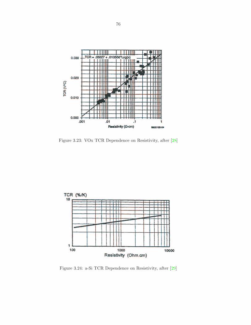
76
Figure 3.23: VOx TCR Dependence on Resistivity, after [28]
Figure 3.24: a-Si TCR Dependence on Resistivity, after [29]

77
Nor
mal
ized
Res
ista
nce
Exposure to air (min)
1
10 20 30 40 50 60
0
0
0.2
0.4
0.6
0.8
Figure 3.25: Pyrolyzed Parylene Resistance Change Upon Exposure to Air
the effect of humidity on the resistivity, a resistance made of a 1µm-thick parylene film
pyrolyzed at 650C was placed into a vacuum chamber with flowing N2 for 2 hours. Air
was then allowed to flow into the chamber. Figure 3.25 shows the normalized resistance as
a function of time since air started to fill the chamber.
In another experiment the resistance was measured in air with a temperature varying
from 110C to 20C. A temperature-controlled chuck with heating and cooling capability
was used in order to reach temperature set-points quickly. Figure 3.26 shows the resistance
as a function of temperature. As can be seen on this figure the resistance starts to drop
, around 36C and at 20C, the resistance is lower than what it was at 120C. Since the
drop starts at a temperature higher than the air temperature, this drop cannot be due to
condensation on the surface and 20C is still above the dew point (the relative humidity
was estimated to be 60%). Measurement made in N2 do not exhibit this drop (see Figure
3.21).
3.3 Conclusion
We have conducted a series of experiments involving the pyrolysis of parylene using
different pyrolysis temperatures. Pyrolysis of parylene above 500C leads to films of glassy
carbon having a resistivity than can be tuned over an 11 orders of magnitude range depend-

78
Res
ista
nce
(Ω)
Temperature (C)
2 ∗ 107
4 ∗ 107
6 ∗ 107
8 ∗ 107
1 ∗ 108
20 40 60 80 100 120
Figure 3.26: Pyrolyzed Parylene Resistance in Air
Parameter Range
Density (g.cm−3) 1.3 < d < 2.2
Young’s Modulus (Pa) 109 < E < 1010
Contact Angle () 80 < θ < 62
Resistivity @300K (Ω.cm) 10−2 < ρ < 109
Contact Resistance @300K (Ω.cm−2) 10−4 < ρc < 106
TCR (%.K−1) 0.3 < |α| < 4
Table 3.6: Summary of Key Properties of Pyrolyzed Parylene

79
ing on the maximum temperature. Data suggests that after the pyrolysis occurs (around
500C), films of pyrolyzed-parylene experience changes in structure and become more and
more crystalline as the temperature is further increased. The TCR was found to be rela-
tively high, between −0.3%.K−1 and −4%.K−1 depending on the pyrolysis temperature.
We showed that pyrolyzed-parylene can easily be integrated into standard microfabrication
processes. Lithography techniques and etching techniques can be used to pattern pyrolyzed
films and to obtain free-standing structures. Table 3.6 summarizes some parameters of
interest for pyrolyzed-parylene. The data shown in this chapter leads us to conclude that
some properties of pyrolyzed-parylene make it attractive to be used in uncooled bolometers.
Chapter 4 discusses such a device.

80
Bibliography
[1] S. C. S. Inc., “Parylene specifications and properties.”
http://www.scscookson.com/parylene knowledge/specifications.cfm. xiv, 54,
56, 57, 58
[2] Specialty Coating Systems Cookson Inc., PDS2010 Parylene Deposition System User’s
Manual. 54
[3] Y. Xu and Y. Tai, “Selective deposition of parylene c for underwater shear-stress sen-
sors,” in Digest of technical papers, Transducers’03, the 12th International Conference
Solid-State Sensors, Actuators and Microsystems, June 2003. 55
[4] E. Charlson and E. C. R. Sabeti, “Temperature selective deposition of parylene-c,”
IEEE Transactions on Biomedical Engineering, vol. 39, pp. 202–206, February 1992.
55
[5] M. Liger, D. Rodger, and Y. Tai, “Robust parylene-to-silicon mechanical anchoring,” in
Proceedings of The 16th IEEE International MEMS Conference (MEMS’03), pp. 602–
605, January 2003. 56
[6] C. Chiang and M. A. C. P. D. Fraser, “Challenges and issues of low-k dielectrics,”
in Proceedings of Technical Papers, International Symposium on VLSI Technology,
Systems, and Applications, pp. 37–39, June 1997. 57
[7] M. Liger, N. Pornsinsirirak, Y. Tai, S. Ho, and C. Ho, “Large-area electrostatically-
valved skins for adaptive flow control on ornithopter wings,” in Technical Digest, Solid
State Sensor and actuator Workshop, pp. 247–250, June 2002. 57
[8] T. Yao, K. Walsh, and Y. Tai, “Dielectrics charging effects on parylene electrostatic

81
actuators,” in Proceedings of the Fifteenth IEEE International Conference on Micro
Electro Mechanical Systems (MEMS ’02), pp. 614–617, January 2002. 57
[9] P. Chen, D. Rodger, M. Humayun, and Y. Tai, “Spiral-tube parylene intraocular pres-
sure sensor,” in Digest of Technical Papers, 18th IEEE International Conference on
MicroElectroMechanical Systems (MEMS 2005), (Miami FL), January-February 2005.
58
[10] J. Xie, J. Shih, Q. He, C. Pang, Y. Tai, Y. Miao, and T. Lee, “An integrated lc-
esi chip with electrochemical-based gradient generation,” in Proceedings of the 17th
IEEE International Conference on MicroElectroMechanical Systems (MEMS 2004),
(Maastricht, The Netherlands), pp. 334–337, January 2004. 58
[11] Wiktionary, “pyrolysis.”
http://en.wiktionary.org/wiki/pyrolysis. 58
[12] T. Edison, “Electric lamp,” January 1880. US Patent 223,898. 58
[13] G. Learmont, L. Nabi, G. Bramham, and J. Bailey, “Pyrolyzis of phenol-formaldehyde
resins .1.,” Plastics & Polymers, vol. 37, no. 129, pp. 201–, 1969. 58
[14] M. Inagaki, T. Ibuki, and T. Takeichi, “Carbonization behavior of polyimide films with
various chemical structures,” Journal of Applied Polymer Science, vol. 44, pp. 521–525,
january 1992. 58
[15] O. Schueller, S. Brittain, C. Marzolin, and G. Whitesides, “Fabrication and character-
ization of glassy carbon mems,” Chem. Mater., vol. 9, pp. 1399–1406, 1997. 58
[16] J. Kim, X. Song, K. Kinoshita, M. Madou, and R. White, “Electrochemical studies of
carbon films from pyrolyzed photoresist,” J. Electrochem Soc, vol. 145, July 1998. 58
[17] S. Ranaganathan, R. McCreery, S. M. Majji, and M. Madou, “Photoresist-derived
carbon for microelectromechanical systems and electrochemical applications,” Journal
of The Electrochemical Society, vol. 147, no. 1, pp. 277–282, 2000. xiv, 58, 59, 67, 70
[18] T. Wang and A. Lal, “Suspended carbon bridges as onchip tunable resistors,” in Digest
of Technical Papers, The 10th International Conference of Solid-State Sensors and
Actuators (transducers’99), (Sendai, Japan), June 1999. 59
82
[19] E. Hui, C. Keller, and R. Howe, “Carbonized parylene as a conformal sacrificial layer,”
in Technical Digest of the 8th Solid-State Sensor and Actuator Workshop, pp. 256–260,
1998. 59
[20] S. Miserendino, S. Boland, and Y. C. Tai, “Material and electrochemical properties of
pyrolyzed parylene-c,” in 206th Meeting of the Electrochemical Society, October 2004.
xii, 61, 63, 64
[21] S. C. S. Inc., “Product specifications, a-174 silane promotion.” 66
[22] W. K. W and D. Puotinen, “Cleaning solutions based on hydrogen peroxide for use in
silicon semiconductor technology,” tech. rep., 1970. 66
[23] O. Tabata, K. Kawahata, S. Sugiyama, , and I. Igarashi, “Mechanical property mea-
surements of thin-films using load deflection of composite rectangular membranes,”
Sensors and Actuators, vol. 20, pp. 135–141, 1989. 68
[24] L. van der Pauw, “A method of measuring the resistivity and hall coefficient of lamellae
of arbitrary shape,” tech. rep., Philips, 1958. 70
[25] A. Walton, “Microelectronic test structures,” tech. rep. 70, 71
[26] Cutnell and Johnson, Physics 4th ed. Wiley and Sons. 70
[27] S. Sze, Physics of Semiconductor Devices, Second Edition. John Wiley and Sons, 1981.
71
[28] B.Cole, R.Horning, B.Johnson, K. Nguyen, P. Kruse, and M. Foote, “High-performance
infrared detector arrays using thin film microstructures,” in Proceedings of the Ninth
IEEE International Symposium on Applications of Ferroelectrics.ISAF’94, pp. 653–
656, August 1991. xii, 75, 76
[29] E. Mottin, A. Bain, J. Martin, J. O.-B. S.Bisotto, J. YON, and J. Tissot, “Uncooled
amorphous silicon technology enhancement for 25µm pixel pitch achievement,” Infrared
Technology and Applications XXVIII, SPIE, vol. 4820, 2002. xii, 75, 76
[30] L. J. Collier, W. S. Stiles, and W. G. A. Taylor, “The variation with temperature of
the electrical resistance of carbon and graphite between 0 c. and 900 c.,” Proceedings

83
of the Physical Society, vol. 51, no. 1, pp. 147–152, 1939.
http://stacks.iop.org/0959-5309/51/147. 75

84
Chapter 4
Uncooled Pyrolyzed-ParyleneCarbon Bolometer
Introduction
This chapter presents a novel uncooled, all-parylene bolometer. The device is made of
two layers of pyrolyzed parylene and a metal layer for interconnections only. We demonstrate
that high responsivity can be achieved by tailoring the electrical conductivity and the TCR
using different pyrolysis conditions for each parylene layer.
4.1 Design
Figure 4.1 shows a typical resistive uncooled bolometer: a free-standing temperature-
sensitive element is linked to a substrate by low thermal conductance legs. Equations
2.27 and 2.65 show the expression of the DC responsivity and the NETD of such a device
(Chapter 2):
ℜ(V.m−1) =∆V (Φ)
Φ=
αηR0Ib
Gth, (2.27)
NETD(K) =4F 2Vn
Adℜ(
dMdT
)
T,[λ1−λ2]
, (2.65)
where α is the TCR of the sensing element, R is the bolometer resistance, Gth is the pixel-
to-substrate thermal conductance, and η is the bolometer absorptivity. The thermal time
constant is given by Equation 2.31:
τth ≡ Cth
Gth, (2.31)

85
Incoming Radiation
Metal Electrode
Suspension Leg
Absorber/Thermistor
Figure 4.1: Typical Bolometer Design
where Cth is the thermal capacitance. The key parameters to obtain good responsivity are:
high TCR α, low Gth and low voltage noise Vn. However, as we try to decrease the thermal
conductance, we must be able to decrease the thermal capacitance, as failure to do so would
result in unacceptably high thermal time constant. To be useful for thermal imaging with
a video frame rate (30Hz), the thermal time constant should be kept below 30ms.
The suspension legs are usually made of silicon nitride or polysilicon. In the case of
silicon nitride legs, it is necessary to have another layer for electrical conduction.
Most uncooled bolometers use vanadium oxide (VOx) [1] or amorphous silicon (a-Si) [2]
as the temperature-sensitive material, reaching a TCR of about 1.5% to 3%[3]. Another
possible material is yttrium-barium-copper oxide (YBaCuO), also reaching TCRs as high
as 3% at room temperature [4].
As shown in Chapter 3, the electrical resistivity of pyrolyzed parylene can be adjusted
over a very wide range (from at least 1010Ω.cm down to 10−2Ω.cm), while the TCR of such
films varies between 0.3%.K−1 and 4%.K−1. We also showed in Chapter 3 that free-standing
structures of pyrolyzed-parylene can be achieved.
Carbon was already being used as a detector material in cooled bolometers several
decades ago. In 1959, W.S. Boyle and K.F. Rodgers reported a cooled carbon bolometer
made of a “thin” layer of carbon (48µm) and having an area of 19mm2. The obtained
responsivity was ℜ = 104V.W−1 and the detectivity was D∗ = 4.25 ∗ 1010[5]. In 1965

86
Shepard described a similar experiment, reaching a responsivity of ℜ = 2.1 ∗ 104V.W−1[6].
In this work we propose a carbon bolometer using pyrolyzed parylene both for the
temperature-sensing element and for the suspension legs. To the author’s best knowledge,
this is the first time a micromachined carbon bolometer and micromachined carbon bolome-
ter array are reported.
Figure 4.2 shows the proposed design. Since our ultimate goal is to build an uncooled
infrared camera, some bolometers had a geometry similar to that shown on Figure 4.1.
There are major differences with the typical “textbook” bolometer design:
• The temperature-sensing element is made of parylene pyrolyzed at low temperature,
leading to a high resistivity and high TCR.
• The suspension leg is made of parylene pyrolyzed at high temperature, leading to a
low resistivity.
There are a number of advantages to this design compared to the traditional design.
• The fabrication process is very simple.
• The bolometer is self-supporting, there is no “dead” thermal conductance or thermal
capacitance due to a supporting layer.
• There is no need for a quarter-wavelength cavity, the wavelength range is extended.
• The suspension legs participate in the absorbtion of incoming radiation.
• There are no positive-TCR metal electrodes, and all section of the bolometer have a
negative TCR.
The main disadvantage of this design the fact that is not compatible with Complementary
Metal-Oxide-Semiconductor (CMOS) or bipolar circuits due to the high-temperature re-
quired for parylene pyrolysis. Only hybrid integration with electronic circuitry is possible.
We chose −2%.K−1 as the target TCR, a value comparable to that found in typical
semiconducting bolometers [1, 7]. For such a TCR, the second layer of parylene must have a
resistivity on the order of 102Ω.cm. Therefore the target thickness of the pyrolyzed parylene
film was chosen to be 2000A. The obtained sheet resistance will then be ρ¤ ∼ 5MΩ. In

87
Thermistor: High-Resistivity Pyrolyzed Parylene
Suspension: Low-Resistivity Pyrolyzed Parylene
Figure 4.2: Two-level Pyrolyzed-Parylene Bolometer Design
theory, it would be possible to use only one layer of high-resistivity pyrolyzed parylene layer,
serving both as thermistor and suspension; however, this would lead to an unreasonable
bolometer resistance. We chose the resistivity of the suspension layer to be in the order of
10−2Ω.cm and its thickness to be 8000A. The sheet resistance for such a resistivity and
thickness is ρ¤ ∼ 125Ω. The absorber size was chosen to be 50∗50µm2. The total bolometer
resistance is given by
R = 2Rleg + Rpixel. (4.1)
The number of resistance squares (ratio between length and width) of the absorber region is
1. Bolometers with different suspension geometry were designed with lengths ranging from
50µm to 170µm, while the width was constant and equal to 5µm. The number of resistance
squares for these suspension dimensions is therefore between 20 to 68. Given the ratio of
resistivity between the two layers of pyrolyzed-parylene, the resistance of the absorber area
is three orders of magnitude higher than the suspension legs. Therefore, the total bolometer
resistance is by far dominated by the absorber area. This ensures a higher relative change
in resistance ∆R/R for a given absorbed radiant flux. Even though the responsivity is
proportional to the absolute change of resistance ∆R, a higher relative change in resistance
is easier to measure using either a voltmeter or an analog-to-digital converter (ADC).

88
Silicon Parylene
1st PPAr
2d PPar
Ti/Au Silicon Dioxide
Figure 4.3: Fabrication Process Flow
4.2 Fabrication
4.2.1 Process Flow
The device process, as shown in Figure 4.3, begins with a 5000A oxide growth and
patterning. A 3µm-thick parylene-C layer is then deposited and pyrolyzed in a nitrogen
atmosphere. The temperature is raised to 800C at 10C/min and then cooled to room
temperature at 2C/min. The resulting film is patterned to define the suspension legs. The
pyrolyzed-parylene etching is done in a Technics PEIIA plasma etcher with 400W of power
and an O2 pressure of 200mT . A 1.4µm layer of AZ1518 photoresist is used as mask. A
second layer of parylene (0.8µm) is deposited and pyrolyzed at 660C at 10C/min. For
better repeatability, the samples are being kept at the maximum pyrolysis temperature for 2
hours. The second layer of pyrolyzed parylene is patterned to define the pixel area. Next, a
Ti/Au interconnection layer (60A/2000A) is evaporated and patterned by wet etching using
photoresist as a mask. Finally, the bolometers are released by Xenon Difluoride (XeF2)
gas-phase etching. In order to fully release the bolometers, an etch depth of 25µm should

89
50µm
50µm50µm
50µm
(Unreleased)
Figure 4.4: XeF2-Released Fabricated Pyrolyzed-Parylene Bolometers
be sufficient. However, due to a slight anisotropy of XeF2 etching, we used an etch depth
of about 60µm. Figure 4.4 shows some fabricated devices.
4.2.2 Processing Issues
Typically, parylene depositions involve a prior coating of A174 for adhesion promotion
[8]. However, it was found that this procedure leads to poor adhesion of the films after
pyrolysis. On the other hand, the adhesion of pyrolyzed parylene on SiO2/Si wafers that
have not been coated with A174 was excellent. This is also part of the reason why we
chose to pattern the parylene after pyrolysis rather than the opposite. It was also observed
that pyrolysis of pattern parylene leads to undesirable border effects, probably due to the
pyrolysis-induced stress. Finally, due to the isotropic etching, patterning the parylene after
it has been shrunk (4 to 5 times) by pyrolysis minimizes undercut. As mentioned earlier, for
a good adhesion between the pyrolyzed-parylene films and the substrate it is crucial that
the substrate be clean prior to parylene depositions. Therefore, an RCA-1 cleaning was
performed before each parylene deposition. As can be seen on Figure 4.3, the second layer

90
Figure 4.5: Bolometer Chip Wire-bonded in PGA Package
of parylene is directly in contact with first layer. No etch-stop layer can be used because
the two layers of parylene must be in electric contact. Therefore, the etching of the second
layer of parylene must be timed accurately to avoid etching the first layer of parylene as
well.
4.3 Results
4.3.1 Electric Parameters
First, the bolometer chips were mounted in a Pin-Grid Array (PGA) package and wire
bonded (Figure 4.5). The respective sheet resistance of both pyrolyzed layers were mea-
sured using van der Pauw “Greek-cross” structures [9] and an Hewlett-Packard HP4145B
semiconductor parameters analyzer as a current source and voltage monitor. The contact
resistance between the pyrolyzed parylene layers and titanium/gold was measured using
Kelvin structures [10], again using an HP4145B semiconductor parameters analyzer as a
current source and voltage monitor. The contact between the layers of pyrolyzed parylene
and titanium/gold was found to be ohmic with a specific contact resistance of 3.5∗10−3Ω.cm2
for the first layer and 3.5Ω.cm2 for the second layer. The TCR of the second parylene layer
was measured in a oven with flowing N2 to avoid having measurement errors to humidity
(see Section 3.2.5.4). The TCR around room temperature was measured to be −1.63%/K.
Table 4.1 shows different characteristics of interest for the two pyrolyzed-parylene layers.
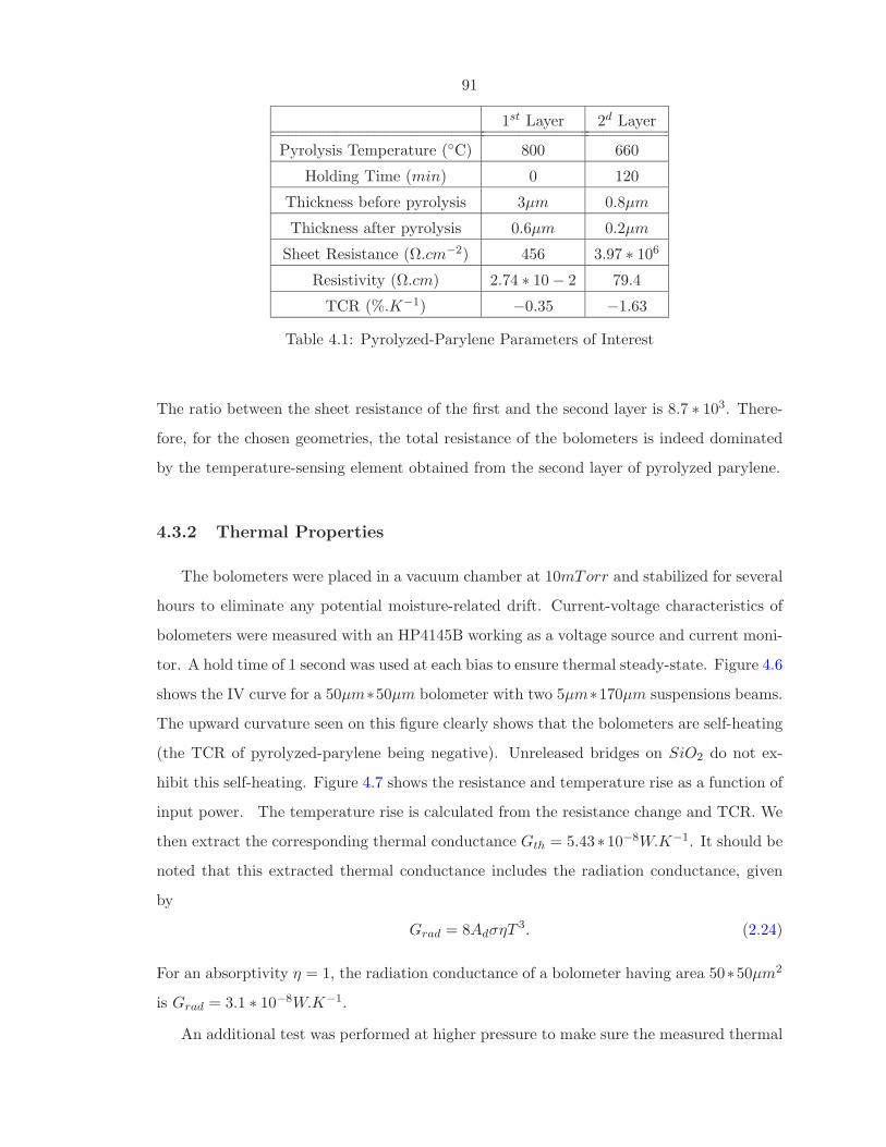
91
1st Layer 2d Layer
Pyrolysis Temperature (C) 800 660
Holding Time (min) 0 120
Thickness before pyrolysis 3µm 0.8µm
Thickness after pyrolysis 0.6µm 0.2µm
Sheet Resistance (Ω.cm−2) 456 3.97 ∗ 106
Resistivity (Ω.cm) 2.74 ∗ 10 − 2 79.4
TCR (%.K−1) −0.35 −1.63
Table 4.1: Pyrolyzed-Parylene Parameters of Interest
The ratio between the sheet resistance of the first and the second layer is 8.7 ∗ 103. There-
fore, for the chosen geometries, the total resistance of the bolometers is indeed dominated
by the temperature-sensing element obtained from the second layer of pyrolyzed parylene.
4.3.2 Thermal Properties
The bolometers were placed in a vacuum chamber at 10mTorr and stabilized for several
hours to eliminate any potential moisture-related drift. Current-voltage characteristics of
bolometers were measured with an HP4145B working as a voltage source and current moni-
tor. A hold time of 1 second was used at each bias to ensure thermal steady-state. Figure 4.6
shows the IV curve for a 50µm∗50µm bolometer with two 5µm∗170µm suspensions beams.
The upward curvature seen on this figure clearly shows that the bolometers are self-heating
(the TCR of pyrolyzed-parylene being negative). Unreleased bridges on SiO2 do not ex-
hibit this self-heating. Figure 4.7 shows the resistance and temperature rise as a function of
input power. The temperature rise is calculated from the resistance change and TCR. We
then extract the corresponding thermal conductance Gth = 5.43∗10−8W.K−1. It should be
noted that this extracted thermal conductance includes the radiation conductance, given
by
Grad = 8AdσηT 3. (2.24)
For an absorptivity η = 1, the radiation conductance of a bolometer having area 50∗50µm2
is Grad = 3.1 ∗ 10−8W.K−1.
An additional test was performed at higher pressure to make sure the measured thermal

92
Voltage (V )
Curr
ent
(nA
)
100
00
200
300
400
500
600
0.2 0.4 0.6 0.8 1.0 1.2 1.4 1.6 1.8
Figure 4.6: Bolometer I-V Characteristic
10
12
14
16
0
2
4
6
8
3.0 ∗ 106
3.2 ∗ 106
3.4 ∗ 106
3.6 ∗ 106
3.8 ∗ 106
4.0 ∗ 106
0.2 0.4 0.6 0.8 10
Dissipated Power (µW )
Tem
peratu
reIn
crease(C
)(calcu
lated)
Res
ista
nce
(Ω)
(mea
sure
d)
Figure 4.7: Bolometer Electrothermal Behavior
93
conductance was indeed that of the suspension legs. The thermal conductivity of an ideal
gas is given in Equation 4.2 [11]
κ =nlvCv
3, (4.2)
where n is the density, l is the mean free path, v the mean particle velocity, and Cv the
specific heat. The thermal conductivity of nitrogen (usually assumed to be the same as air)
is κ = 0.026 W.m−1.K−1. One may intuitively think that heat conductivity is proportional
to density or at least decreases with decreasing density: such an intuition would be wrong.
The expression of the mean free path is
l =1
σcn, (4.3)
where σc is the cross-sectional area for the gas considered. Since the mean free-path is
inversely proportional to density, Equation 4.2 can be reduced to
κ =vCv
3σc. (4.4)
Therefore, the thermal conductivity of a ideal gas is independent of pressure. However, this
is only true as long as the mean free-path is much larger than the dimensions of the system
considered [1, 12]:
l =50µm
p(Torr). (4.5)
Therefore for a pressure p = 10mTorr the mean free path is 5mm, which is much larger
than the gap between the bolometers and the bottom of the cavity.
The bolometers were then placed into a vacuum oven at 100Torr with bleeding N2.
The evolution of the bolometers resistance as a function of input power was measured,
in an experiment similar to that described above. Figure 4.8 and 4.9 show the obtained
electrothermal behavior of bolometers whose suspensions are 170µm∗5µm and 70µm∗5µm,
respectively. The thermal conductance of both pixels is two orders of magnitude higher
than that measured at a pressure of 10mTorr. The expected thermal conductance for a
gap d = 50µm and an absorber area of Ad = 50µm ∗ 50µm is
Gth = κAd
d= 1.3 ∗ 10−6(W.K−1). (4.6)

94
The measured thermal conductances are a few times higher than the calculated ones, which
may be due to convection.
4.3.2.1 Thermal Conductivity
Next the bolometers were placed in a vacuum chamber with having a Zinc Sulfide (ZnS,
also called Cleartran R©) window obtained from ISP Optics.1 The chamber was pumped
down to a pressure below 20mTorr. ZnS has an external transmittance between 60% and
70% from 0.5µm to 14µm. A calibrated pyroelectric detector was was used to estimate the
absorptivity of the bolometers. An IR-55 thermal infrared source obtained from Boston
Electronics.2 was used to produce pulsed infrared radiation. The infrared source was
biased with a square wave at 15Hz with 50% duty cycle. The bolometers were biased
with a constant current of 300nA. A Stanford Research Systems3 SR785 dynamic signal
analyzer was used as a spectrum analyzer to observe the 15Hz voltage component. The
signal was then compared to that of a P1−71 precision pyroelectric detector obtained from
Coherent Incorporated.4 (formerly Molectron) under the same conditions. The pyroelectric
detector was calibrated by the manufacturer and the given responsivity at 15Hz was 7.09 ∗104V.m−1 (after the built-in amplification). The absorptivity was estimated to be around 0.6
(assuming the same amount of radiation was indeed incident on both the bolometer and the
pyroelectric detector). The radiation conductance for such a absorptivity is Grad = 1.86 ∗10−8W.K−1. The corresponding Gleg for the bolometer having a suspension 5µm ∗ 170µm
is Gleg = 3.57 ∗ 10−8W.K−1. From this value, we estimated the thermal conductivity of the
suspension legs:
Gleg = 2κtw
L,
κ =GlegL
2tw
κ = 0.76W.m−1.K−1.
The thermal conductivity reported here is about two times lower than the conductivity
reported in [13]. This is because in [13] the calculation was made without taking the
1http://www.ispotics.com2http://www.boselec.com/3http://www.thinksrs.com4http://www.coherent.com

95
Gth = 5.7 ∗ 10−6W.K−1
Figure 4.8: Bolometer Electrothermal Behavior at 100Torr
Gth = 5.9 ∗ 10−6W.K−1
Figure 4.9: Bolometer Electrothermal Behavior at 100Torr

96
radiation conductance into account. Therefore, the calculation made here is more accurate.
However, as mentioned before this calculation relies on the estimation of the absorptivity,
which is only a rough estimation. This is lower than than values reported for silicon nitride
deposited using Plasma Enhanced Chemical Vapor Deposition (PECVD) [14, 15], with the
major advantage of providing electrical conductivity. It is also one order of magnitude lower
than polysilicon. [16].
4.3.2.2 Thermal Capacitance and Thermal Capacity
An optical chopper wheel was used to measure the thermal time constant of the bolome-
ters. The bolometers were biased with a constant current of 300nA. A Stanford Research
Systems5 SR785 dynamic signal analyzer was used as a spectrum analyzer to observe funda-
mental voltage component for different chopping frequencies. As expected from the theory,
the bolometers exhibit a first order response, as shown in Figure 4.10. The corresponding
time constant is extracted to be be τth = 12.9ms. From this value and that of the thermal
conductance, we calculate the thermal capacitance Cth, the volumic heat capacity Cv, and
the specific heat C.
Cth = τthGth = 1.2 ∗ 10−9J.K−1,
Cv =Cth
Adt= 2.3J.cm−3,
C =Cv
d= 1.5J.g−1,
where t = 0.2µm is the thickness of the absorber and d the density. Using a result from
Section 3.2.4.1 we chose to assume d = 1.5g.cm−3
4.3.3 Noise
The 1/f noise of bolometers having a resistance 1.5MΩ was measured using low-noise
amplifiers and a Stanford Research Systems6 SR785 dynamic signal analyzer to measure
the low-frequency power spectral density. Batteries were used as power supply to avoid
introducing additional noise, and the whole circuit was put in a metal enclosure. The
internal voltage source of the SR785 was used to generated different voltage biases. The
5http://www.thinksrs.com6http://www.thinksrs.com

97
10 200.4
0.6
0.8
1
Chopping Frequency (Hz)
Nor
mal
ized
Res
pon
sivity
Gth = 9.15 ∗ 10−8W.K−1
Suspension Legs Dimensions: 70 ∗ 6µm2
Absorber Dimensions: 50 ∗ 50µm2
Figure 4.10: Bolometer Dynamic Response
R
Bolometer
Low-noise
AmplifierLow-noise
Amplifier
Dynamic Signal Analyzer
FFTADC
Input noise: HznV /10
Input impedance: ΩM1
DC Source
Rl
Figure 4.11: 1/f Noise Measurement Setup
input-referred noise of the instrument is 10nV.Hz−1/2 when used in its small input range
(−50dBVpk). Therefore, the circuit was connected to the dynamic signal analyzer with
a 1µF capacitor in order to be able to use that range. The instrument having an input
impedance of 1MΩ, the cut-off frequency of the high-pass filter is 0.16Hz. Figure 4.11
shows the measurement circuit. The noise power contributions of both the amplifiers and
the dynamic signal analyzer are both on the order of 10−16V 2.Hz−1, one order of magnitude
lower than the Johnson noise contribution of each resistor (4.14∗10−15V 2.Hz−1). Assuming
we can ignore the contributions from the amplifiers and from the dynamic signal analyzer,
the noise power measured by the instrument is
Smeasured(f) = kTR + kTRl +Sf (f)
4, (4.7)

98
−110
−105
−115
−120
−125
−130
−135
−140
2.51.25 2.251.5 1.75 2.752 3.0
0.1V1.1V2V
4V
log(f(Hz))
Sbolo(f)(dB)
Figure 4.12: Bolometer 1/f Noise Power Spectrum
where Rl is the load resistor, R is the bolometer resistance, and Sf (f) is the 1/f noise power
spectral density. The load resistance Rl is chosen to match the bolometer resistance of the
bolometer (to reach optimum power transfer). In this experiment, the bolometer resistance
was 1.5MΩ. Figure 4.12 shows the noise power spectrum Sbolo generated by the bolometer
for biasing voltages between 0.1V and 4V , with
Sbolo = 4 ∗ (Smeasured − kTRl). (4.8)
As can be seen on Figure 4.12, at Vb = 0.1V , the noise is dominated by Johnson noise.
The level of this Johnson noise was extracted to be 2.8 ∗ 10−14V 2.Hz−1. This is more than
the expected value 4kTR = 1.66 ∗ 10−14V 2.Hz−1. Thinking it could be because the noise
added by the amplifier and/or the dynamic signal analyzer, a plain metal resistor of 1MΩ
was swapped with the bolometer. The noise power found then was very close to the noise
power given by Nyquist formula.
The 1/f noise was found to follow the form
Sf =A(Vb)
fγ, (4.9)

99
1 ∗ 10−11
2 ∗ 10−11
3 ∗ 10−11
4 ∗ 10−11
5 ∗ 10−11
31 2 4
KV 2b
Vb
A(Vb)
Figure 4.13: Noise Power Factor Evolution as a Function of Bias
where A is a constant that depends on the biasing voltage Vb. We found that 0.98 <
γ < 1.06 for all measured spectrum but with no trend that indicated a dependence on the
biasing voltage. Therefore, for the rest of this analysis we chose to use γ = 1. Figure 4.13
shows the evolution of the noise power factor A(Vb) as a function of bias. The continuous
curve represents a parabolic fit with K = 3.3 ∗ 10−12 V −2. We conclude that Sf (f) =
3.3∗10−12V 2
b
f is a reasonable model for the 1/f generated by the bolometer and, if anything,
an overestimation since the extra white noise might not come from the bolometer.
4.3.4 Analysis
Table 4.2 summarizes key properties of a bolometer having suspension legs 70µm∗5µm,
i.e., a number of electric and thermal conduction squares of 14. Similar electric and thermal
properties should then be obtained with suspensions having dimensions 50µm∗3.6µm. Some
parameters were obtained by measurements presented in this section. Others, including the
responsivity ℜ and the NETD, were calculated using definitions from Section 2.3. The
parameters are compared with those reported for VOx bolometer in [1]. Even though the
responsivity is higher in the work presented here, the NETD for the same integration time
(5µs) is close to three times higher. For the VOx bolometer, an integration time τpulse = 5µs
and a biasing voltage of 5V leads to a temperature increase
∆Tpulse ≃Vb
2
R0Cthτpulse = 2K. (4.10)

100
However, because the pyrolyzed-parylene bolometer has a much higher resistance, the same
biasing voltage leads to a much smaller temperature increase, about 26mK. Furthermore,
because the films of pyrolyzed-parylene were prepared at high temperatures, we expect
them to be able to withstand higher temperature increases during readout than VOx can.
Therefore, longer integration times could be used for the carbon bolometer.
For an integration time τpulse = 100µs, the NETD of our bolometer is reduced to 47mK,
which is comparable to that of the VOx bolometer. However, in imaging applications an
array of bolometers needs to be completely read during each frame period (33ms). Having
a longer integration time is therefore more demanding in term of the number of analog-
to-digital required. Figure 4.14 shows the calculated noise contributions as a function of
Parameter This Work [1]
Suspension Dimensions 70µm ∗ 5µm 50µm ∗ 2µm
Suspension Material 0.8µm Pyrolyzed Parylene 0.8µm Silicon Nitride
Absorber Dimensions 50µm ∗ 50µm 35µm ∗ 35µm
Absorber Material 0.2µm Pyrolyzed Parylene 0.8µm Silicon Nitride
Resistance 3.9MΩ 20KΩ
TCR α −1.63%.K−1 −2.3%.K−1
Sensing Material Pyrolyzed Parylene VOx
Thermal Conductance Gth 9.6 ∗ 10−8 W.K−1 2 ∗ 10−7 W.K−1
Thermal Capacitance Cth 1.2 ∗ 10−9 J.K−1 3 ∗ 10−9 J.K−1
Time Constant τ 12.5ms 15ms
Absorptivity η 0.6 0.8
Responsivity ℜ (D.C.) 5.12 ∗ 105V.W−1 4 ∗ 105V.W−1
NETD1 109 mK 39 mK
NETD2 47 mK −1 calculated for Vb = 5V , τpulse = 5µs and 1/f noise limit f1 = 10−3Hz
2 calculated for Vb = 5V , τpulse = 100µs and 1/f noise limit f1 = 10−3Hz
Table 4.2: Summary of Bolometer Parameters
voltage bias. As can be seen, for biases Vb < 2.6V the Johnson noise is dominating. However,
both 1/f noise voltage and responsivity are proportional to the biasing voltage, while the
Johnson noise is constant. Therefore, as the biasing voltage keeps increasing, the total
noise becomes dominated by the 1/f noise and the NETD approaches the 1/f noise-limited

101
T Fluct.Johnson
1/f
Bias (V )
Total Noise
NETD NE
TD
(mK
)
Vol
tage
Noi
se(µ
V)
0
00
0
00
0
00
0
0
0
0
0
0
0
00
1
1
1
2
2
2
2
3
3
3
4
4
5
5
5
5
5
6
Figure 4.14: Noise Contributions for τpulse = 100µs
NETD of Equation 2.77. Given thermal conductance, the temperature fluctuation noise is
always one order of magnitude lower than the 1/f noise.
4.4 Conclusion
We have successfully fabricated uncooled infrared sensors with a simple two-layer pyrolyzed-
parylene process. Electrothermal study shows that pyrolyzed-parylene is a promising can-
didate to replace silicon nitride and polysilicon for the thermal insulation, and that it can
also be used to achieve high-TCR thin films for the pixel.

102
0
20
20
40
40
100
100
120
120 140
80
80
60
60
NETD(mK)
τpulse (µs)
Johnson Noise Dominating
1/f Noise Dominating
Figure 4.15: NETD for Varying Integration Time for Vb = 5V
103
Bibliography
[1] R. A. Wood, “Uncooled infrared imaging systems,” in Semiconductor and Semimetals
(D. D. Skatrud and P. W. Kruse, eds.), vol. 47, ch. 3, Academic Press, 1997. 85, 86,
93, 99, 100
[2] J. Tissot, “Ir detection with uncooled focal plane arrays. state of the art and trends,”
Opto-Electronics Review, vol. 12, no. 1, p. 105109, 2004. 85
[3] A. Rogalski, “Infrared detectors: Status and trends,” Progress in Quantum Electronics,
vol. 27, no. 2, pp. 59–210, 2003. 85
[4] A. Jahanzeb, C. Travers, Z. Celik-Butler, D. Butler, and S. Tan, “A semiconduc-
tor ybacuo microbolometer for room temperature ir imaging,” IEEE Transactions On
Electron Devices, vol. 44, pp. 1795–1801, October 1997. 85
[5] W. Boyle and K. Rodgers Journal of The Optical Society of America, vol. 49, no. 66,
1959. 85
[6] G. Shepard, “Static response characteristics for a carbon bolometer,” Journal of Ap-
plied Physics, vol. 36, October 1965. 86
[7] M. Almasri, D. Butler, and Z. Celik-Butler, “Self-supporting uncooled infrared mi-
crobolometers with low-thermal mass,” Journal of Microelectromechanical Systems,
vol. 10, pp. 469–476, September 2001. 86
[8] S. C. S. Inc., “Product specifications, a-174 silane promotion.” 89
[9] L. van der Pauw, “A method of measuring the resistivity and hall coefficient of lamellae
of arbitrary shape,” tech. rep., Philips, 1958. 90
[10] A. Walton, “Microelectronic test structures,” tech. rep. 90

104
[11] D. W. Stops, “The mean free path of gas molecules in the transition regime,” J. Phys.
D: Appl. Phys., vol. 3, 1970. 93
[12] X. He, T. Mei, W. Neuzil, and U.Sridhar, “Performance of microbolometer focal plane
arrays uner varying pressure,” IEEE Electron Device Letters, vol. 21, May 2000. 93
[13] M. Liger, S. Konishi, and Y. Tai, “Uncooled all-parylene bolometer,” in Technical
Digest of The 17th IEEE International MEMS Conference (MEMS’04), pp. 593–596,
2004. 94
[14] M. von Arx, O. Paul, and H. Baltes, “Process-dependent thin-film thermal conduc-
tivities for thermal cmos mems,” Journal Of Microelectromechanical Systems, vol. 9,
March 2000. 96
[15] S. Hafizovic and O. Paul, “Temperature-dependent thermal conductivities of cmos
layers by micromachined thermal van der pauw test structures,” Sensors and Actuators
A, vol. 97, no. 8, pp. 246–252, 2002. 96
[16] A. McConnell, S. Uma, and K. Goodson, “Thermal conductivity of doped polysilicon
layers,” Journal of Microelectromechanical Systems, vol. 10, pp. 360–369, September
2001. 96

105
Chapter 5
Uncooled Carbon Thermal Imager
This chapter presents a 1024 pixel parylene-pyrolyzed thermal imager. Using results
from previous chapters, we designed and fabricated a 32 ∗ 32 array of carbon bolometers.
Using infrared optics, we demonstrate for the first time the potential of this technology for
uncooled thermal imaging.
5.1 Design
5.1.1 Pixel Layout
Figure 5.1 shows the pixel layout. The pitch distance was chosen to be 75µm in both
directions. The main limitation for this number was the lithography and mask-making
resolution. Nothing in the technology itself prevents us from fabricating arrays with a
smaller pitch. The absorber area is 50µm ∗ 50µm and is linked to the substrate by two
suspension legs having dimensions 60µm ∗ 2.8µm each. The fill factor is therefore 44.4%.
On each pixel one suspension leg is connected to a “column” metal electrode (vertical line
on Figure 5.1) while the other is connected to a “row” metal electrode (horizontal line on
Figure 5.1). The two metal layers are insulated by a layer of parylene (non-pyrolyzed). The
silicon underneath the absorber and suspension legs is removed to make the bolometers free-
standing, while the metal electrodes and their contact with the suspension legs are deposited
on silicon dioxide. Therefore, the silicon must be removed anisotropically in order to not
undercut the metal electrodes.

106
Column Electrodes
Row Electrodes
Low-Resistivity P.P. High-Resistivity P.P.
Insulation Parylene
Silicon DioxideSilicon
75µm
Figure 5.1: Pixel Layout
5.2 Fabrication
Two fabrication processes were explored in this work: a dry-etch bulk micromachining
process and a wet-etch bulk micromachining process. Even though the wet process eventu-
ally proved to provide much better results, we present the dry process, as it may find some
use for other applications.
5.2.1 Dry-Etch Bulk Micromachining Process
The Dry-Etch bulk micromachining process was the first process attempted in order to
fabricate pyrolyzed-parylene bolometer arrays. There were two reasons for preferring dry
etching a priori as opposed to wet etching: First, the interface between parylene and silicon
or silicon dioxide is often reported to not withstand wet anisotropic etchants like Potassium
Hydroxide (KOH) or Tetramethyl Ammonium Hydroxide (TMAH). Second, because the
layers of pyrolyzed-parylene are only tenths of a micron in thickness, there was some concern
that stiction would be unavoidable.
The main challenge when designing the dry-etch process was that we needed the bolome-
ters to be freestanding, and therefore, needed the silicon underneath them to be undercut.

107
Silicon Silicon Dioxide
Low-Resistivity P.P. High-Resistivity P.P.
Cr/Au
(a)
(b)
(c)
(d)
(e)
(f)
(g)
(h)
Figure 5.2: Process-Flow for Dry Release
At the same time, the silicon underneath the metal lines could not be undercut. To address
this challenge, we developed a “Deep Shallow Trench Isolation” process, somewhat similar
to the Shallow Trench Isolation (STI) process used to isolate devices in integrated circuits.
However, in our case “isolation” stands for chemical insulation rather than electrical insu-
lation.
The dry-etch bulk micromachining process flow is shown on Figure 5.2. First, Deep-
Reactive Ion etching (DRIE) is used to etch trenches into the silicon substrate (a). Those
trenches were 2µm in width. Then the trenches were filled with silicon dioxide in a thermal
oxidation furnace (b). This is made possible by the conformality of silicon thermal oxidation.
Also, because only 56% the silicon dioxide actually grows “out” of the silicon surface [1],
1.8µm of silicon dioxide growth are required to fill a 2µm-wide trench. In the next step,

108
chemical-mechanical polishing (CMP) is used to delayer the silicon dioxide while providing
a smooth surface for further processing (c).
A thin layer of thermal oxide is then grown to serve as electrical insulation (d). This
oxide is patterned to leave the silicon exposed where the absorber and suspension legs are
destined to be (e). A 4µm-thick layer of parylene C is deposited, pyrolyzed at 800C, and
patterned by Reactive Ion Etching (RIE) (O2 plasma) to define the suspension legs (f).
As expected from previous experiments presented in Chapter 3, the pyrolyzed films shrunk
to a thickness of 0.8µm. A second layer of parylene C, 2.4µm in thickness, is deposited
pyrolyzed at 640C for 120 minutes and finally patterned to define the absorber area (g).
The thickness after pyrolysis is 0.6µm. A layer of chrome/gold/chrome (50A/1000A/50A)
is then deposited using a lift-off process. Because a thermal evaporator was used for this
last step and because step coverage is needed, the wafers are titled at various angle during
evaporation.
After an A174 silane coating is applied on the wafers [2] and a thin layer of parylene
C (0.3µm) is deposited and patterned to serve as insulation between the column metal
layer and the row metal layer. According the parylene dimer manufacturer, the dielectric
strength for parylene C is 2.21 ∗ 106V.cm−1; therefore, this insulation should theoretically
allow for voltage biases up to 66.3V . The chrome/gold (50A/2000A) row metal layer is
deposited using lift-off. Finally, the bolometers are released using XeF2 gas-phase etching
(h).
As mentioned in Chapter 3, having clean surfaces are essential to obtain good adhesion
of parylene and pyrolyzed-parylene to their substrate. For this reason, RCA − 1 cleaning
is used before each of the three parylene depositions. Great precaution must be taken
when releasing the bolometers. If etching is allowed to take place for too long, the etching
front will reach the end of the silicon dioxide “isolation” trenches and the whole array will
eventually be released.
The yield for the dry-etch process was found to be very small. Even though some ar-
rays were successfully released, only about 70% of bolometers were operable. Also, long
exposure to XeF2 was found to damage the chrome/gold/chrome and chrome/gold elec-
trodes. Therefore, the dry-etch was abandoned and the wet-etch process described in the
next section was preferred.

109
Silicon Silicon Dioxide
Low-Resistivity P.P. High-Resistivity P.P.
Cr/Au
(a)
(b)
(c)
(d)
Figure 5.3: Process-Flow for Wet Release
5.2.2 Wet-Etch Bulk Micromachining Process
The Wet-Etch process described here uses TMAH. One remarkable property of TMAH
silicon etching is that the etching of concave corners of (111) planes intersections while the
convex corners are etched [3]. Also, TMAH is compatible with metals, and it was found that
if appropriate precautions are taken, parylene/silicon dioxide interfaces do not delaminate.
Therefore, using TMAH etching allows for the releasing of the bolometers while preserving
the row and column metal lines as well as the silicon underneath them.
The Wet-Etch process can be seen in Figure 5.3. This process is much simpler and
shorter than the dry-etch process. It begins with the growth of a thin layer of thermal
oxide usede as electrical insulation and as mask for the final TMAH release. The rest of
the process is very similar to the dry-etch fabrication process after its second silicon dioxide
growth. A 4µm-thick layer of parylene C is deposited, pyrolyzed at 800C, and patterned
by RIE (O2plasma) to define the suspension legs (b). The thickness of the pyrolyzed-film
was 0.8µm as expected. A second layer of parylene C, 2.4µm in thickness is deposited,
pyrolyzed at 640C for 120 minutes, and finally patterned to define the absorber area (c).
The etching of the second layer of pyrolyzed-parylene must be timed carefully to avoid over-
etching the first layer, which is unprotected. The thickness of the first layer of pyrolyzed
parylene decreased to 0.75µm after the second layer patterning. The thickness of the second

110
Figure 5.4: Pixel Before Release
pyrolyzed-parylene film was 0.6µm. A layer of chrome/gold/chrome (50A/1000A/500A) is
deposited using a lift-off process to define the column metal layer. After applying an A174
silane coating as adhesion promoter on the wafers [2], a thin layer of parylene C (0.3µm) is
deposited and patterned to serve as insulation between the column metal layer and the row
metal layer. Again, because the two layers of pyrolyzed-parylene are unprotected during
the insulation parylene etching, this etching must be timed carefully. The first layer of
pyrolyzed-parylene after the insulation parylene patterning was 0.65µm and the thickness
of the second pyrolyzed film was 0.4µm. The chrome/gold (50A/2000A) row metal layer is
deposited using lift-off. Figure 5.4 shows a pixel and part of its neighbors at this step of
the process (right before release).
After dicing, the bolometers are released in a 15% solution of TMAH taken to 90C in
a reflux system. The chips are rinsed for 15min in a water tank before they are immersed
in methanol. In order to avoid stiction, the chip must not be allowed to dry. Each chip
is finally dried using CO2 supercritical drying in a Tousimis system. Figure 5.5 shows a
released array at different magnifications.

111
(a) (b)
(c) (d)
75µm
75µm
75µm
750µm
Figure 5.5: Release Bolometer Array

112
5.3 Characterization
5.3.1 Electrical Properties
First, the resistance of the bolometers was measured in N2 and at low bias to avoid
self-heating. The resistance across a 12 ∗ 11 array was 3.8MΩ on average with a standard
deviation of 421KΩ. This mediocre uniformity could be due to inaccuracy in the mask-
making process. However, it should be noted that in a bolometer array, uniformity of dark
resistance is not crucial. More important is the uniformity of responsivity (hence uniformity
of thermal conductance). Thickness measurements across the 32 ∗ 32 array showed good
thickness uniformity. The average resistivity, calculated assuming the contributions the
suspension leg resistance were negligible, was ρ = 3.04 ∗ 102Ω.cm.
The TCR of the bolometers was measured in an oven with flowing N2 using a precision
thermocouple as reference. The TCR was measured to be α = −2.1%, which is what could
be expected from the resistivity.
5.3.2 Thermal Properties
The arrays were then placed into a vacuum chamber at 20mTorr and allowed to stabilize
for 2 hours to desorb any moisture. The current-voltage characteristic was measured using
an Hewlett-Packard HP4145B semiconductor parameters analyzer. During such testing,
attention must be paid to the power dissipated by the bolometers as the bolometers experi-
ence an increase in temperature that is proportional to this power. In our experiments, the
power dissipated was kept lower than 0.5µW . Figure 5.6 shows the relationship between
dissipated power and resistance for a bolometer pixel. Since the resistance change is given
by
∆R = αR0P
Gth, (5.1)
the data represented in Figure 5.6 gives us a direct measurement of α/Gth. The ther-
mal conductance was then calculated using the previously measured TCR, leading to a
value Gth = 6.1 ∗ 10−8W.K−1. The absorptivity was measured using a EDO Corpora-
tion Infrascope (infrared microscope). The obtained absorptivity was η ≃ 0.6. However
this piece of equipment actually measures the absorptivity from 1µm to 5.5µm. As-
suming the carbon acts as a graybody, the radiation conductance is calculated to be

113
Dissipated Power (10−7W )
Pix
elR
esis
tance
(MΩ
)0.0 1.0 2.0 3.0 4.0
3.2
3.3
3.4
3.5
3.6
3.7
Figure 5.6: Bolometer Pixel Power-Resistance Relationship
Grad = 1.86 ∗ 10−8W.K−1. The thermal conductance of the suspension legs is then cal-
culated to be Gleg = 4.24 ∗ 10−8W.K−1 (or 2.12 ∗ 10−8W.K−1 for each leg). This is less
than what could be expected from the suspension dimensions (60µm ∗ 2.8µm ∗ 0.8µm) and
thermal conductivity reported in 4.3.2. This discrepancy is due to the fact that the ac-
tual width of the suspension legs is between 1.5µm and 2µm due to undercut during the
etching as well as some exposure to O2 plasma during the etching of the second layer of
pyrolyzed-parylene and insulation parylene.
In an experiment similar to that presented in Section 4.3.2, the bolometers’ thermal time
constant was measured using a light chopping wheel at various frequencies. The thermal
constant was found to be 31ms, which with the value of Gth previously measured allows
us to calculate the thermal capacitance to be Cth = 1.9 ∗ 10−9J.K−1. The obtained time
constant is close to the period corresponding to 30Hz (33ms). Therefore, the responsivity
will drop for signals close to that frequency. However, this could be solved by reducing the
pixel thickness (although this could lead to a decrease in absorptivity). From the TCR,
absorptivity, and thermal conductivity the responsivity can be calculated using Equation
2.27:
ℜ =αηVb
Gth= 1.03 ∗ 106V.W−1,
for Vb = 5V .

114
Frequency (Hz)
Noi
sePow
erSpec
tral
Den
sity
(V2.H
z−
1)
3V
4V
5V
10−10
10−11
1 10
Figure 5.7: Low Noise Power Spectrum
5.3.3 Noise
The noise of individual pixels was measured using a dynamic signal analyzer as explained
in Section 4.3.3. Figure 5.7 shows a typical 1/f noise spectrum for different biasing voltages.
This measurement was performed in air. The extracted noise factor extracted from this data
is K = 6.4∗10−12, higher than the noise reported in Chapter 3. One reason could be that the
resistivity of the pyrolyzed-parylene is about four times higher than the pyrolyzed-parylene
used in the single-element bolometer. It is well-known that materials with higher resistivity
usually have higher 1/f noise.
5.3.4 Performance
Table 5.1 shows the calculated noise contributions of Johnson noise, 1/f noise and
temperature fluctuation noise for Vb = 5V , F = 1 and a limit to 1/f noise f1 = 10−3Hz.
Similar to the single-pixel bolometer presented in Chapter 3, the noise in the array is
dominated by Johnson noise for an integration time τpulse = 5µs and by 1/f noise if
τpulse = 100µs. The corresponding NETD are 57mK and 31mK respectively. 31mK is very
close to state of the art bolometers (it is actually a little better than the VOx bolometer
reported in [4]). However, for an array of 320 ∗ 200 = 64000 pixels, an integration time
of 100µs would require 193 analog-to-digital converters in order to read all pixels within

115
τpulse = 5µs τpulse = 12µs τpulse = 100µs
Johnson Noise (µV ) 79.3 51.2 17.7
1/f Noise (µV ) 54.0 52.6 49.3
Temperature Fluctuation Noise (µV ) 2.7 2.7 2.7
Total Noise(µV) 96.0 73.5 52.5
NETD 57mK 44mK 31mK
Table 5.1: Bolometer Noise Contributions
one frame period of 33.3ms. As explained in Section 2.5.5, once the integration time is
long enough for the noise to be dominated by 1/f noise, little is gained from increasing it
further. A good trade-off value for the integration time is when the Johnson noise and the
1/f noise contributions are equal:
KVb2(3
2− γ − ln(2πf1τpulse)
)
= 4kTR0(1
2τpulse− f1) (5.2)
τpulse = 11.3µs. (5.3)
Using this integration time leads to an NETD of 44mK and would require 24 analog to
digital converters, which is a more reasonable number.
Table 5.2 shows a summary of parameters for the pyrolyzed-parylene carbon bolometer
array compared with the V Ox bolometer array of [4].
5.4 Thermal Imaging
5.4.1 Testing Setup
Figure 5.8 shows the testing setup used to produce infrared images. The chips are
mounted on a flange facing a Zinc Sulfide (ZnS) window obtained from ISP Optics Corpo-
ration.1 Zinc sulfide has an external transmittance between 60% and 70% between 0.5µm
and 14µm. An array of 24 electrical feedthroughs was made in another flange using vacuum
epoxy. This limits the thermal imaging capability to 12 ∗ 11 pixels (the last feedthrough
begin used for grounding). Figure 5.9 shows the bolometer array mounted on its flange and
seen through the ZnS window.
1http://www.ispotics.com

116
Parameter This Work [4]
Pitch 75µm 50µm
Suspension Dimensions 60µm ∗ 2µm 50µm ∗ 2µm
Suspension Material 0.8µm Pyrolyzed Parylene 0.8µm Silicon Nitride
Absorber Dimensions 50µm ∗ 50µm 35µm ∗ 35µm
Fill Factor 44% 70%
Absorber Material 0.5µm Pyrolyzed Parylene 0.8µm Silicon Nitride
Resistance 3.8MΩ 20KΩ
TCR α −2.1%.K−1 −2.3%.K−1
Sensing Material Pyrolyzed Parylene VOx
Thermal Conductance Gth 6.1 ∗ 10−8 W.K−1 2 ∗ 10−7 W.K−1
Thermal Capacitance Cth 1.9 ∗ 10−9 J.K−1 3 ∗ 10−9 J.K−1
Time Constant τ 31ms 15ms
Absorptivity η 0.6 0.8
Responsivity ℜ (D.C.) 1.03 ∗ 106V.W−1 4.6 ∗ 105V.W−1
NETD1 57mK 39mK
NETD2 44mK −NETD3 31mK −
1 Calculated with Vb = 5V , F = 1, τpulse = 5µs and a limit to 1/f noise f1 = 10−3Hz2 Calculated with Vb = 5V , F = 1, τpulse = 12µs and f1 = 10−3Hz3 Calculated with Vb = 5V , F = 1, τpulse = 100µs and f1 = 10−3Hz
Table 5.2: Summary of Bolometer Array Parameters

117
AMTIR Lens
ZnS Window
To Vacuum Pump
x
yz
24Fee
thro
ugh
s
Thermal Imager Chip
Figure 5.8: Schematic of Testing Setup
Figure 5.9: Thermal Imager Chip Seen Through ZnS Window

118
Figure 5.10: AMTIR Lens
An F/1.5 Amorphous Material Transmitting Infrared (AMTIR2) lens with focal length
38mm (obtained from Newport Corporation3) is mounted on an x-y-z stage outside of the
vacuum chamber. The external transmittance of AMTIR is greater than 60% from 1µm to
14µm. Figure 5.10 shows the lens.
Figure 5.11 shows the circuit used to read each pixel. A voltage bias is applied to one
row at a time. Each column electrode is connected to an operational amplifier used as an
inverting amplifier. The voltage at the output of an amplifier is given by
V = −VbRl
R, (5.4)
where Rl is the feedback resistance used in the inverting amplifier.
A Hewlett-Packard HP34970A data acquisition system was used together with a 34903A
20-channel actuator module to apply the biasing voltage on the desired row and a 34901A
20-channel multiplexer to measure the voltage of the desired column. The HP34970A was
remotely controlled with a computer through its General Purpose Interface Bus (GPIB).
A C++ software was written to selectively access the pixels. In “continuous” mode the
resistance of a given pixel is monitored continuously and can be saved. The resistance
change expected from infrared illumination being smaller than the variation of resistance
across the array, a calibration was necessary. To calibrate the array a “dark-image” mode
was implemented. In this mode the resistance of each pixel is measured sequentially and
saved. In an “image” mode the resistance of each pixel is measured and subtracted from
the resistance measured in “dark-image” mode. The image is then displayed and saved.
Figure 5.12 shows a screen capture of the software, while the radiation of a flashlight was
2Ge33As12Se55
3http://www.newport.com
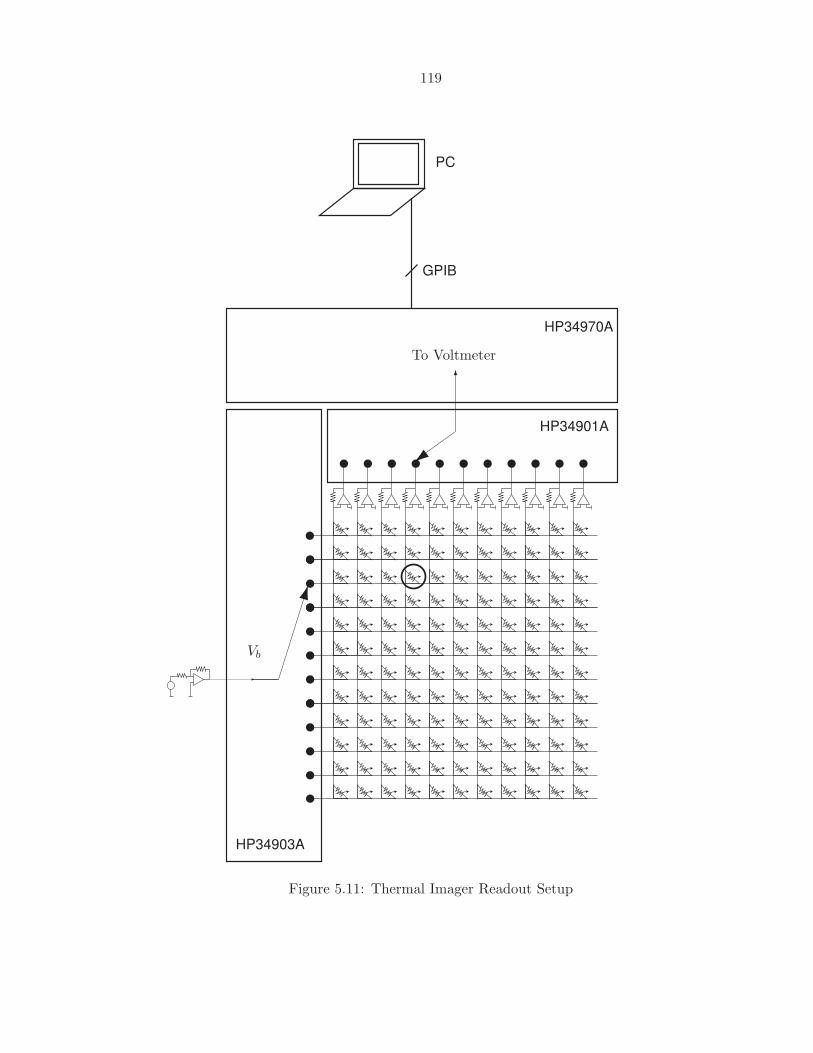
119
HP34903A
HP34901A
HP34970A
GPIB
PC
Vb
To Voltmeter
Figure 5.11: Thermal Imager Readout Setup

120
Figure 5.12: Readout Software
focused on the array.
5.4.2 Results
A 50W regular visible lamp was used to focus the array. The light was directed to the
array and the position of the lens was adjusted using the x-y-z stage while monitoring the
voltage on the central pixel continuously. Once the maximum voltage change is obtained,
the lamp is replaced with the desired target. Figure 5.12shows a screen capture of the
software window after an image was read.
Because the electronics were outside of the vacuum chamber, far away from the bolome-
ters, a lot of noise is picked up during readout, although it does not come from the bolome-
ters themselves. Therefore, only hot surfaces > 100C were captured.
Figure 5.13 shows the tip of a soldering iron at a 3m distance.
1
f=
1
zi+
1
zo
zi =fzo
zo − f= 38.5mm,
where f is the focal length of the lens, zo the object distance, and zi the image distance.

121
Figure 5.13: Soldering Iron Tip at 3m
The magnification factor is
M =zi
zo= 1.28 ∗ 10−2.
therefore each pixel correspond to an object area of 5.9mm and the total image area is
7.1cm ∗ 6.5cm.
Figure 5.14 shows thermal images obtained by arranging power resistors arranged in a
“C” and an “O” pattern, as well as the same image after spatial interpolation. The maxi-
mum change of resistance in Figure 5.14 was −3.6%. Note that pixel (3, 9) is consistently
darker than its neighbors. After inspection under microscope, it was found that a piece of
debris was thermally shorting the absorber and the column electrode. For all arrays tested
the pixel operability was better than 98%.
5.5 Conclusion
We have designed, fabricated, and tested a carbon bolometer array based on two layers
of pyrolyzed-parylene. Test results show good responsivity, acceptable noise, and high pixel
operability. However, resistance uniformity remains an issue, and the thermal constant
(31ms) should be decreased for optimal operation at video frame rate.

122
1 2 3 4 5 6 7 8 9 10 11
1 2 3 4 5 6 7 8 9 10 11
1
2
3
4
5
6
7
8
9
10
11
12
1
2
3
4
5
6
7
8
9
10
11
12
Figure 5.14: Power Resistors at 3m

123
Calculations show that if the same design was used in a 320 ∗ 200 array using an inte-
gration time of 12µs the NETD for F/1 optics would be 44mK which is very close to the
state of the art. Such an array would require 24 analog to digital converters. This is very
encouraging considering that this is the first reported carbon microbolometer. The thermal
imaging functionality was demonstrated on a 12 ∗ 11 subset of the array.
124
Bibliography
[1] S. Wolf and R. Tauber, Silicon Processing for the VLSI Era. Lattice Press, 1986, vol. 1.
107
[2] S. C. S. Inc., “Product specifications, a-174 silane promotion.” 108, 110
[3] G. Kovacs, N.I.Maluf, and K. Petersen, “Bulk micromachining of silicon,” in Proceedings
of the IEEE, vol. 86, no. 8, August 1998, pp. 1536–1551. 109
[4] R. A. Wood, “Uncooled infrared imaging systems,” in Semiconductor and Semimetals,
D. D. Skatrud and P. W. Kruse, Eds. Academic Press, 1997, vol. 47, ch. 3. 114, 115,
116

125
Chapter 6
Conclusion and Future Directions
In this work we have demonstrated how pyrolysis of parylene can be used to fabricate
carbon microbolometers for uncooled thermal imaging on a chip and to produce carbon
films that are easily integrated in standard microfabrication processes. We then showed
that the properties of pyrolyzed-parylene carbon can be process-tuned to produce films
with different electrical and thermal properties. Resistivity can be tuned between 109Ω.cm
and 10−2Ω.cm, while the temperature coefficient of resistance changes from 4%.K−1 to
0.3%.K−1.
We fabricated a novel all-carbon microbolometer with a unique design using two layers
of pyrolyzed parylene. Using the tunability of pyrolyzed-parylene carbon, we produced films
with low electrical resistivity yet low thermal conductivity to serve as thermal insulation,
while the absorber part of the bolometer was made out of carbon having high resistivity
and a high temperature coefficient of resistance. With this design, the resistance of the
whole device is dominated by the temperature-sensitive part while achieving high thermal
insulation. After having characterized the various properties of the carbon microbolometer,
including their excess noise, we set out to fabricate a 32 ∗ 32 array of carbon bolometers
for thermal imaging applications. Using a wet bulk micromachining process we obtained
arrays a pixel operability greater than 98% and a responsivity to infrared light of 106V.W
for a 5V bias. We then demonstrated the thermal imaging functionality by taking thermal
images using an infrared lens. Calculation using noise measurement results show that the
sensitivity to target temperature (NETD) can be as low as 31mK and 44mK for 100µs and
12µs electrical signal integration time, respectively. This is very close to the current state
of the art of microbolometers.
Future possible directions include the development of a surface-micromachined process

126
to improve the optical fill factor and absorptivity as well as reducing the pixel dimensions.
More importantly, novel processes of reducing the 1/f noise in pyrolyzed-parylene carbon
films should be explored, as it is the current performance-limiting factor. Possible strategies
include annealing or the use of special gases during pyrolysis, e.g., forming gas. Another
challenge is integration with electronics. The current process does not allow for monololithic
integration with CMOS or bipolar electronics to high temperature processing steps. Ways
of locally converting polymer films into carbon films with appropriate properties could be
one way to solve this problem, e.g, using laser.

127
Index
1/f Noise, 33
A-174, 66
Adhesion, 66
Arrhenius, 74
Background Noise, 36
Blackbody, 19
Blackbody Exitance, 20
Boltzmann, Ludwig Eduard, 2
Camera Equation, 24
Conformality, 55
Contact Angle, 68
Contact Resistance, 71
Density, 67
Detectivity, 38
Differential Scanning Calorimetry (DSC),
61
Edison, Thomas, 58
Electrical-Thermal Analogy, 24
Exitance, 17
F-number, 24
Flicker Noise, 33
Herschel, William, 1
Hooge, F.N., 34
Humidity, 77
Intensity, 17
Irradiance, 16
Johnson Noise, 32
Johnson, J.B., 32
Joulean Heating, 29
Kelvin Structure, 71
Lambertian Surface, 18
Langley, Samuel Pierpont, 15
NETD, 38
Nobili, Leopoldo, 8
Noise Bandwidth, 31
Noise Equivalent Power, 37
Noise-Equivalent Temperature Difference,
38
Nyquist, Harry, 32
Parylene, 54
Patterning, 66
Planck, 19
Planck Blackbody Radiation Law, 19
Planck, Max Karl Ernst Ludwig, 2
Platinum, 60
Projected Area, 16
Pyrolysis, 58

128
Radiance, 16, 20
Radiant Flux, 16
Radiation Conductance, 26
Radiation Transfer, 21
RCA Cleaning, 66
Readout, 29
Resistivity, 70
Roughness, 68
Seebeck,Thomas Johann, 8
Solid Angle, 17
Stefan-Boltzmann, 20
Stiction, 110
Stress, 67
Supercritical Drying, 110
TCR, 27, 74
TEM, 61
Temperature Coefficient of Resistance (TCR),
27
Temperature Fluctuation Noise, 36
Temperature Sensitivity, 74
Theoretical Limitations, 40
Thermal Conductance, 27
Thermal Noise, 32
Thermal Time Constant, 29
Thermogravimetric Analysis (TGA), 61
TMAH, 109
Van der Pauw Structures, 70
Weight Loss, 60
Wien’s Displacement Law, 21
Wien, Wilhelm, 2
Young’s modulus, 67


![Research Article Simulation and Analysis of Uncooled ...analysis of uncooled microbolometer begins by solving the heat balance equation that can be expressed as [ ] + = BIAS + IR,](https://static.fdocuments.in/doc/165x107/60c493a8fa135514ac128252/research-article-simulation-and-analysis-of-uncooled-analysis-of-uncooled-microbolometer.jpg)

