UM2283 User manual - Home - STMicroelectronics · September 2017 DocID030972 Rev 1 1/33 UM2283...
30
Introduction The STEVAL-IPMnM2N is a compact motor drive power board based on SLLIMM-nano™ (small low-loss intelligent molded module) IPM MOSFET-based (STIPN2M50T-H). It provides an affordable and easy-to-use solution for driving high power motors for a wide range of applications such as power white goods, air conditioning, compressors, power fans and 3-phase inverters for motor drives in general. The IPM itself consists of short-circuit rugged MOSFETs and a wide range of features like undervoltage lockout, smart shutdown, embedded temperature sensor and NTC, and overcurrent protection. The main characteristics of this evaluation board are small size, minimal BOM and high efficiency. It consists of an interface circuit (BUS and V CC connectors), bootstrap capacitors, snubber capacitor, hardware short-circuit protection, fault event and temperature monitoring. In order to increase the flexibility, it is designed to work in single- or three-shunt configuration and with triple current sensing options: three dedicated onboard op-amps, an internal IPM op-amp and op-amps embedded in the MCU. The Hall/Encoder section completes the circuit. With these advanced characteristics, the system is designed to achieve fast and accurate current feedback conditioning, satisfying the typical requirements for field-oriented control (FOC). The STEVAL-IPMnM2N is compatible with ST's STM32-based control board, enabling designers to build a complete platform for motor control. Figure 1. Motor control board (top view) based on SLLIMM-nano™ MOSFET 100 W motor control power board based on STIPN2M50T-H SLLIMM™nano IPM UM2283 User manual UM2283 - Rev 2 - May 2018 For further information contact your local STMicroelectronics sales office. www.st.com
-
Upload
truonghanh -
Category
Documents
-
view
221 -
download
5
Transcript of UM2283 User manual - Home - STMicroelectronics · September 2017 DocID030972 Rev 1 1/33 UM2283...

IntroductionThe STEVAL-IPMnM2N is a compact motor drive power board based on SLLIMM-nano™ (small low-loss intelligent moldedmodule) IPM MOSFET-based (STIPN2M50T-H). It provides an affordable and easy-to-use solution for driving high powermotors for a wide range of applications such as power white goods, air conditioning, compressors, power fans and 3-phaseinverters for motor drives in general. The IPM itself consists of short-circuit rugged MOSFETs and a wide range of features likeundervoltage lockout, smart shutdown, embedded temperature sensor and NTC, and overcurrent protection.
The main characteristics of this evaluation board are small size, minimal BOM and high efficiency. It consists of an interfacecircuit (BUS and VCC connectors), bootstrap capacitors, snubber capacitor, hardware short-circuit protection, fault event andtemperature monitoring. In order to increase the flexibility, it is designed to work in single- or three-shunt configuration and withtriple current sensing options: three dedicated onboard op-amps, an internal IPM op-amp and op-amps embedded in the MCU.The Hall/Encoder section completes the circuit.
With these advanced characteristics, the system is designed to achieve fast and accurate current feedback conditioning,satisfying the typical requirements for field-oriented control (FOC).
The STEVAL-IPMnM2N is compatible with ST's STM32-based control board, enabling designers to build a complete platform formotor control.
Figure 1. Motor control board (top view) based on SLLIMM-nano™ MOSFET
100 W motor control power board based on STIPN2M50T-H SLLIMM™nano IPM
UM2283
User manual
UM2283 - Rev 2 - May 2018For further information contact your local STMicroelectronics sales office.
www.st.com

1 Key features
• Input voltage: 125 - 400 VDC
• Nominal power: up to 100 W• Nominal current: up to 1.2 Arms
• Input auxiliary voltage: up to 20 VDC
• Motor control connector (32 pins) interfacing with ST MCU boards• Single- or three-shunt resistors for current sensing (with sensing network)• Three options for current sensing: external dedicated op-amps, internal SLLIMM-nano op-amp (single) or
through MCU• Overcurrent hardware protection• IPM temperature monitoring and protection• Hall sensors (3.3 / 5 V)/encoder inputs (3.3 / 5 V)• MOSFET intelligent power module:
– SLLIMM-nano™ IPM MOSFET-based (STIPN2M50T-H - Full molded package package)• Universal design for further evaluation with bread board and testing pins• Very compact size
Figure 2. Motor control board (bottom view) based on SLLIMM-nano™ MOSFET
UM2283Key features
UM2283 - Rev 2 page 2/30

2 Circuit schematics
The full schematics for the SLLIMM-nano™ MOSFET card for STIPN1M50T-H IPM products is shown below. Thiscard consists of an interface circuit (BUS and VCC connectors), bootstrap capacitors, snubber capacitor, short-circuit protection, fault output circuit, temperature monitoring, single-/three-shunt resistors and filters for inputsignals. It also includes bypass capacitors for VCC and bootstrap capacitors. The capacitors are located veryclose to the drive IC to avoid malfunction due to noise.Three current sensing options are provided: three dedicated onboard op-amps, one internal IPM op-amp and theembedded MCU op-amps; selection is performed through three jumpers.The Hall/Encoder section (powered at 5 V or 3.3 V) completes the circuit.
UM2283Circuit schematics
UM2283 - Rev 2 page 3/30

2.1 Schematic diagrams
Figure 3. STEVAL-IPMnM2N circuit schematic (1 of 5)I
np
ut
DC_b
us_v
olta
ge
ST
EV
AL
-I
PM
Nn
tm
p
de
co
de
r
t m p
GM
01
23
56
7
4
89
NQ
3.3
V
+Bus
3.3
V 1.65
V
Bus_
volta
ge
RC
60
0 R
C12
0 R
C14
RC
20
D1
RC
10
+ C4 47
µ/3
5 V
J1
INPU
T-dc1 2
RC
100
RC
70
R2
470K
R312
0R
R1 470K
R6
1k0
-+
U1D
TSV9
94
12 1314
4 11
0 R
C13RC
30
RC
80
0 R
C11
RC
40
+ C3
R4
7k5
C2 10 n
RC
50
RC
90
+C1
R5 1k0
47 µ
/35
V
UM2283Schematic diagrams
UM2283 - Rev 2 page 4/30

Figure 4. STEVAL-IPMnM2N circuit schematic (2 of 5)
Cur
rent
_C_a
mp
Cur
rent
_A
Cur
rent
_B
Cur
rent
_Cph
ase_
A
phas
e_B
phas
e_C
3.3
V+5
V
EM_S
TOP
PWM
-A-H
PWM
-A-L
PWM
-B-H
PWM
-B-L
PWM
-C-H
PWM
-C-L
NTC
_byp
ass_
rela
y
PWM
_Vre
fM
_pha
se_A
M_p
hase
_B
Bus_
volta
ge
M_p
hase
_C
NTC
Cur
rent
_B_a
mpE2 E3
Cur
rent
_A_a
mp
E1
Mot
or O
utpu
tJ3
123
SW2
1
2
3
SW3
1
2
3
Con
trol C
onne
ctor
J2 12
34
56
78
910
1112
1314
1516
17 19 21 23 2526
2728
2930
3132
333418 20 22 24
SW1
12
3
UM2283Schematic diagrams
UM2283 - Rev 2 page 5/30
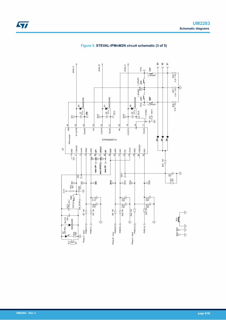
Figure 5. STEVAL-IPMnM2N circuit schematic (3 of 5)
STIPN2M50T-H
0.33
1 W
0.33
1 W
0.33
1 W
UM2283Schematic diagrams
UM2283 - Rev 2 page 6/30

Figure 6. STEVAL-IPMnM2N circuit schematic (4 of 5)
3.3
V
1.65
V
1.65
V
1.65
V
3.3
V
3.3
V
3.3
V
E1
Cur
rent
_A_a
mp
E2
Cur
rent
_B_a
mp
E3
Cur
rent
_C_a
mp
nano
OP+
nano
OP-
nano
OPO
UT
R21
1k0
R20
1k9
-+
U1A
TSV9
94
3 21
4 11
TP24
R22
1k
R33
1k9
C30
100
p
R27
1k0
C29
330
p
R31
1k
C24
100
p
C28
10 n
C25
330p
TP25
-+
U1B
TSV9
94
5 67
4 11
R26
1k0
C23
100
n
C22
10 n
R25
1k9
D10
R24
1k9
R32
1k0
C31
330pTP
26
SW17
1
2
3
R23
1k0
R29
1k9
+
C21
4.7
µ 5
0 V
C27
100
p
-+
U1C
TSV9
94
10 98
4 11
R30
1k0
R28
1k9
C26
10 n
R43
1k
UM2283Schematic diagrams
UM2283 - Rev 2 page 7/30

Figure 7. STEVAL-IPMnM2N circuit schematic (5 of 5)
H3/
Z+H
2/B+
H1/
A+G
ND
+ 3.
3/5
V
Ha
ll
/E
nc
od
er
M_p
hase
_A
M_p
hase
_C
M_p
hase
_B
3.3
V
+5 V
3.3
V
+5 V
R42
4k7
R39
2k4
J5
Enco
der/H
all
11
22
33
44
55
SW12
C37
10 p
SW15
C34
100
n
SW13
SW10
R40
4k7
SW9
1
2
3
R34
4k7
R41
4k7
R35
4k7
C33
100
n
C35
10 p
R37
2k4
SW14
R38
2k4
C32
100
n
SW16
1
2
3
R36
4k7
SW11
C36
10 p
UM2283Schematic diagrams
UM2283 - Rev 2 page 8/30

3 Filters and key parameters
3.1 Input signalsThe input signals (LINx and HINx) to drive the internal MOSFETs are active high. A 375 kΩ (typ.) pull-downresistor is built-in for each input signal. To prevent input signal oscillation, an RC filter is added on each input asclose as possible to the IPM. The filter is designed using a time constant of 10 ns (1 kΩ and 10 pF).
3.2 Bootstrap capacitorIn the 3-phase inverter, the emitters of the low side MOSFETs are connected to the negative DC bus (VDC-) ascommon reference ground, which allows all low side gate drivers to share the same power supply, while theemitter of the high side MOSFETs is alternately connected to the positive (VDC+) and negative (VDC-) DC busduring running conditions.A bootstrap method is a simple and cheap solution to supply the high voltage section. This function is normallyaccomplished by a high voltage fast recovery diode. The SLLIMM-nano 2 MOSFET -based family includes apatented integrated structure that replaces the external diode with a high voltage DMOS functioning as a diodewith series resistor. An internal charge pump provides the DMOS driving voltage.The value of the CBOOT capacitor should be calculated according to the application requirements.Figure 8. CBOOT graph selection shows the behavior of CBOOT (calculated) versus switching frequency (fsw), withdifferent values of ∆VCBOOT for a continuous sinusoidal modulation and a duty cycle δ = 50%.
Note: This curve is taken from application note AN4840 (available on www.st.com); calculations are based on theSTGIP5C60T-Hyy device, which represents the worst case scenario for this kind of calculation.The boot capacitor must be two or three times larger than the CBOOT calculated in the graph.For this design, a value of 2.2 µF was selected.
Figure 8. CBOOT graph selection
UM2283Filters and key parameters
UM2283 - Rev 2 page 9/30

3.3 Overcurrent protectionThe SLLIMM-nano MOSFET -based integrates a comparator for fault sensing purposes. The comparator has aninternal voltage reference VREF (540 mV typ.) connected to the inverting input, while the non-inverting input on theCIN pin can be connected to an external shunt resistor to implement the overcurrent protection function. Whenthe comparator triggers, the device enters the shutdown state.The comparator output is connected to the SD pin in order to send the fault message to the MCU.
3.3.1 SD pinThe SD is an input/output pin (open drain type if used as output) used for enable and fault; it is shared with NTCthermistor, internally connected to GND.The pull-up resistor (R10) causes the voltage VSD-GND to decrease as the temperature increases. To maintainthe voltage above the high-level logic threshold, the pull-up resistor is sized at 1 kΩ (3.3 V MCU power supply).The filter on SD (R10 and C18) must be sized to obtain the desired re-starting time after a fault event and placedas close as possible to the pin.A shutdown event can be managed by the MCU; in which case, the SD functions as the input pin.Conversely, the SD functions as an output pin when an overcurrent or undervoltage condition is detected.
3.3.2 Shunt resistor selectionThe value of the shunt resistor is calculated by the following equation:RSH = VrefIOC (1)
Where Vref is the internal comparator (CIN) (0.54 V typ.) and IOC is the overcurrent threshold detection level.The maximum OC protection level should be set to less than the pulsed collector current in the datasheet. In thisdesign, the overcurrent threshold level is fixed at IOC = 2.6 A in order to select a commercial shunt resistor value.
RSH = Vref ⋅ R15 + R11R11 + VFIOC = 0.54 ⋅ 1000 + 47004700 + 0.182.6 = 0.321 Ω (2)
Where VF is the voltage drop across diodes D3, D4 and D5.For the power rating of the shunt resistor, the following parameters must be considered:• Maximum load current of inverter (85% of Inom [Arms]): Iload(max)
• Shunt resistor value at TC = 25 °C• Power derating ratio of shunt resistor at TSH =100 °C• Safety margin
The power rating is calculated by the following equation:
PSH = 12 ⋅ Iload max2 ⋅ RSH ⋅ marginDerating gratio (3)
The commercial value chosen was 0.66 Ω to which corresponds an overcurrent level of 2.5 A.The power rating is:
• Inom = 2A Inom rms = Inom2 Iload max = 85% Inom rms= 1.2 Arms(4)
• Power derating ratio of shunt resistor at TSH = 100 °C: 80% (from datasheetmanufacturer)• Safety margin: 30% PSH = 12 ⋅ 1.2² ⋅ 0.33 ⋅ 1.30.8 = 0.38W (5)
Considering the commercial value, a 1 W shunt resistor was selected.Based on the previous equations and conditions, the minimum shunt resistance and power rating is summarizedbelow.
UM2283Overcurrent protection
UM2283 - Rev 2 page 10/30

Table 1. Shunt selection
Device Inom(peak) [A] OCP(peak) [A] Iload(max) [Arms] RSHUNT [Ω]Minimum shunt
power rating PSH[W]
STIPN2M50T-H 2 2.5 1.2 0.33 0.38
3.3.3 CIN RC filterAn RC filter network on the CIN pin is required to prevent short-circuits due to the noise on the shunt resistor. Inthis design, the R15-C8 RC filter has a constant time of about 1 µs.
3.3.4 Single- or three-shunt selectionSingle- or three-shunt resistor circuits can be adopted by setting the solder bridges SW5, SW6, SW7 and SW8.The figures below illustrate how to set up the two configurations.
Figure 9. One-shunt configuration
Figure 10. Three-shunt configuration
Further details regarding sensing configuration are provided in the next section.
UM2283Overcurrent protection
UM2283 - Rev 2 page 11/30

4 Current sensing amplifying network
The STEVAL-IPMnM2N motor control evaluation board can be configured to run in three-shunt or single-shuntconfigurations for field oriented control (FOC).The current can be sensed thanks to the shunt resistor and amplified by using the on-board operational amplifiersor by the MCU (if equipped with op-amp).Once the shunt configuration is chosen by setting solder bridge on SW5, SW6, SW7 and SW8 (as described inthe previous section), the user can choose whether to send the voltage shunt to the MCU amplified or notamplified.Single-shunt configuration requires a single op amp so the only voltage sent to the MCU to control the sensing isconnected to phase V through SW2.Switch SW17 is used to send amplified signal coming from the internal IPM op-amp or from an external one.SW1, SW2, SW3 and SW17 can be configured to select which signals are sent to the microcontroller, as per thefollowing table.
Table 2. Op-amp sensing configuration
Configuration Sensing Bridge (SW1) Bridge (SW2) Bridge (SW3) Bridge (SW17)
Single Shunt
IPM op-amp open 1-2 open 2-3
On board op-amp open 1-2 open 1-2
MCU op-amp open 2-3 open 1-2
Three ShuntOn board op-amp 1-2 1-2 1-2 1-2
MCU op-amp 2-3 2-3 2-3 1-2
The operational amplifier TSV994 used on the amplifying networks has a 20 MHz gain bandwidth from a singlepositive supply of 3.3 V.The amplification network must allow bidirectional current sensing, so an output offset VO = +1.65 V representszero current.For the STIPN2M50T-H (IOCP = 2.5 A; RSHUNT = 0.33 Ω), the maximum measurable phase current, consideringthat the output swings from +1.65 V to +3.3 V (MCU supply voltage) for positive currents and from +1.65 V to 0 fornegative currents is:Equation 5 MaxMeasCurrent = ∆Vrm = 2.5 A (6)
rm = ∆VMaxMeasCurrent = 1.652.5 = 0.66 Ω (7)
The overall trans-resistance of the two-port network is:rm = RSHUNT ∙ AMP = 0.33 ∙ AMP = 0.66 Ω (8)
AMP = rmRSHUNT = 0.660.33 = 2 (9)
Finally choosing Ra=Rb and Rc=Rd, the differential gain of the circuit is:AMP = RcRa = 1.9 (10)
An amplification gain of 1.9 was chosen. The same amplification is obtained for all the other devices, taking intoaccount the OCP current and the shunt resistance, as described in Table 1.The RC filter for output amplification is designed to have a time constant that matches noise parameters in therange of 1.5 µs: 4 ∙ τ = 4 ∙ Re ∙ Cc = 1.5 μs (11)
UM2283Current sensing amplifying network
UM2283 - Rev 2 page 12/30

Cc = 1.5 µs4 ∙ 1000 = 375 pF 330 pF selected (12)
Table 3. Amplifying networks
PhaseAmplifying network RC filter
Ra Rb Rc Rd Re Cc
Phase U R21 R23 R20 R24 R22 C25
Phase V R26 R27 R25 R29 R43 C29
Phase W R30 R32 R28 R33 R31 C31
UM2283Current sensing amplifying network
UM2283 - Rev 2 page 13/30
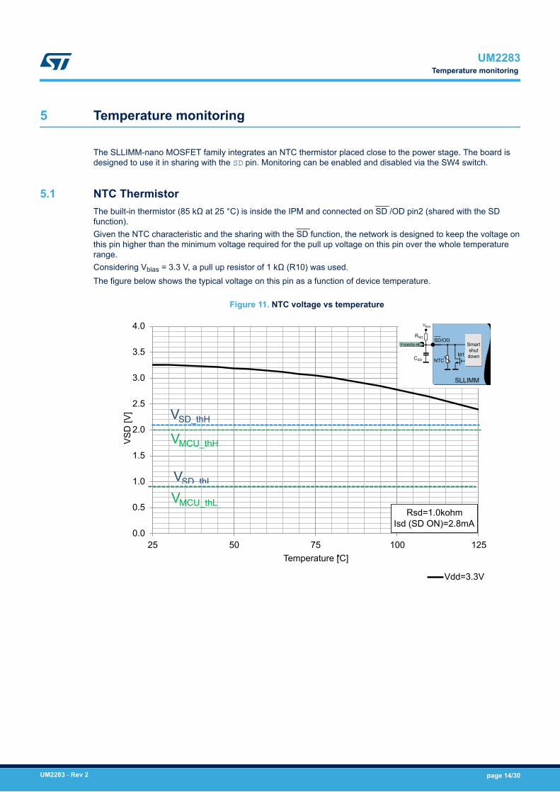
5 Temperature monitoring
The SLLIMM-nano MOSFET family integrates an NTC thermistor placed close to the power stage. The board isdesigned to use it in sharing with the SD pin. Monitoring can be enabled and disabled via the SW4 switch.
5.1 NTC ThermistorThe built-in thermistor (85 kΩ at 25 °C) is inside the IPM and connected on SD /OD pin2 (shared with the SDfunction).Given the NTC characteristic and the sharing with the SD function, the network is designed to keep the voltage onthis pin higher than the minimum voltage required for the pull up voltage on this pin over the whole temperaturerange.Considering Vbias = 3.3 V, a pull up resistor of 1 kΩ (R10) was used.The figure below shows the typical voltage on this pin as a function of device temperature.
Figure 11. NTC voltage vs temperature
0.0
0.5
1.0
1.5
2.0
2.5
3.0
3.5
4.0
25 50 75 100 125
VSD
[V]
Temperature [°C]
Vdd=3.3V
Rsd=1.0kohmIsd (SD ON)=2.8mA
From/to mCSD/OD
M1
Smart shut down
VBias
RSD
CSD
SLLIMM
NTC
VSD_thL
VSD_thH
VMCU_thH
VMCU_thL
UM2283Temperature monitoring
UM2283 - Rev 2 page 14/30

6 Firmware configuration for STM32 PMSM FOC SDK
The following table summarizes the parameters which customize the latest version of the ST FW motor controllibrary for permanent magnet synchronous motors (PMSM): STM32 PMSM FOC SDK for this STEVAL-IPMnM2N.
Table 4. ST motor control workbench GUI parameters - STEVAL-IPMnM2N
Block Parameter Value
Over current protection
Comparator threshold Vref ∙ R15 + R11R11 + VF = 0.83 V (13)
Overcurrent network offset 0
Overcurrent network gain 0.1 V/A
Bus voltage sensing Bus voltage divider 1/125
Rated bus voltage info
Min rated voltage 125 V
Max rated voltage 400 V
Nominal voltage 325 V
Current sensing
Current reading typology Single- or three-shunt
Shunt resistor value 0.33 Ω
Amplifying network gain 1.9
Command stage
Phase U Driver HS and LS: Active high
Phase V Driver HS and LS: Active high
Phase W Driver HS and LS: Active high
UM2283Firmware configuration for STM32 PMSM FOC SDK
UM2283 - Rev 2 page 15/30

7 Connectors, jumpers and test pins
Table 5. Connectors
Connector Description / pinout
J1Supply connector (DC – 125 V to 400 V)
• 1-L - phase• 2 N - neutral
J2
Motor control connector
1 - emergency stop
3 - PWM-1H
5 - PWM-1L
7 - PWM-2H
9 - PWM-2L
11 - PWM-3H
13 - PWM-3L
15 - current phase A
17 - current phase B
19 - current phase C
21 - NTC bypass relay
23 - dissipative brake PWM
25 - +V power
27- PFC sync.
29 - PWM VREF
31 - measure phase A
33 - measure phase B
2 - GND
4 - GND
6 - GND
8 - GND
10 - GND
12 - GND
14 - HV bus voltage
16 - GND
18 - GND
20 - GND
22 - GND
24 - GND
26 - heat sink temperature
28 - VDD_m
30 - GND
32 - GND
34 - measure phase C
J3
Motor connector• phase A• phase B• phase C
J4VCC supply (20 VDC max)
• positive• negative
J5
Hall sensors / encoder input connector1. Hall sensors input 1 / encoder A+2. Hall sensors input 2 / encoder B+3. Hall sensors input 3 / encoder Z+4. 3.3 or 5 Vdc5. GND
Table 6. Jumpers
Jumper Description
SW1
To choose current U to send to control board:
Jumper on 1-2: from amplification
Jumper on 2-3: directly from motor output
UM2283Connectors, jumpers and test pins
UM2283 - Rev 2 page 16/30

Jumper Description
SW2
To choose current V to send to control board
Jumper on 1-2: from amplification
Jumper on 2-3: directly from motor output
SW3
To choose current W to send to control board:
Jumper on 1-2: from amplification
Jumper on 2-3: directly from motor output
SW4 To send or not temperature information, coming from NTC, to micro
SW5, SW6 SW7, SW8
To choose one shunt or 3 shunt configuration. (Through solder bridge)
SW5, SW6 close SW7, SW8 open one shunt
SW5, SW6 open SW7, SW8 close three shunt
SW9, SW16
To choose input power for Hall/Encoder
Jumper on 1-2: 5 V
Jumper on 2-3: 3.3 V
SW10, SW13 To modify phase A hall sensor network
SW11, SW14 To modify phase B hall sensor network
SW12, SW15 To modify phase C hall sensor network
SW17
To choose on board or IPM op-amp in one shunt configuration
Jumper on 1-2: on board op-amp
Jumper on 2-3: IPM op-amp
Table 7. Test pins
Test Pin Description
TP1 OUTW
TP2 HINW (high side W control signal input)
TP3 VccW
TP4 SD (shutdown pin)/NTC
TP5 LINW (high side W control signal input)
TP6 OP+
TP7 OPOUT
TP8 OP-
TP9 VbootW
TP10 OUTV
TP11 NV
TP12 HINV (high side V control signal input)
TP13 VbootV
TP14 LINV (high side V control signal input)
TP15 CIN
TP16 NU
TP17 NW
UM2283Connectors, jumpers and test pins
UM2283 - Rev 2 page 17/30

Test Pin Description
TP18 OUTU
TP19 VbootU
TP20 LINU (high side U control signal input)
TP21 Ground
TP22 Ground
TP23 HinU (high side U control signal input)
TP24 Current_A_amp
TP25 Current_B_amp
TP26 Current_C_amp
TP27 Ground
UM2283Connectors, jumpers and test pins
UM2283 - Rev 2 page 18/30

8 Bill of material
Table 8. Bill of materials
Item Qty Reference Part/Value Description Manufacturer Order code
1 0 C1 330 µF 400 V±10%
Electrolyticcapacitor - DNM EPCOS B43501A9337M000
2 4 C2, C22, C26, C28 10 nF 50 V±10%
Ceramicmultilayercapacitors
AVX 12065C103KAT2A
3 2 C3, C4 47 µF 50 V±20%
Electrolyticcapacitor any any
4 3 C5, C6, C7 2.2 µF 25 V±10%
Ceramicmultilayercapacitors
Murata GCM31MR71E225KA57L
5 1 C8 1 nF 50 V ±10%Ceramicmultilayercapacitors
Kemet C1206C102K5RACTU
6 1 C12 10 µF 50 V±20%
Electrolyticcapacitor AVX 12061A100JAT2A
7 9 C10, C11, C14, C15, C16,C19, C35, C36, C37
10 pF 100 V±10%
Ceramicmultilayercapacitors
AVX 12061A100JAT2A
8 1 C17 0.1 µF 630 V±10%
Ceramicmultilayercapacitor
Murata GRM43DR72J104KW01L
9 1 C18 3.3 nF 50 V±10%
Ceramicmultilayercapacitor
Kemet C1206C332K5RACTU
10 1 C21 4.7 µF 50 V±20%
Electrolyticcapacitor any any
11 3 C24, C27, C30 100 pF 100 V±10%
Ceramicmultilayercapacitors
Kemet C1206C101J1GACTU
12 3 C25, C29, C31 330 pF 50 V±10%
Ceramicmultilayercapacitors
AVX 12065A331JAT2A
13 5 C13, C23, C32, C33, C34 100 nF 50 V±10%
Ceramicmultilayercapacitors
AVX 12065C104KAZ2A
14 5 D1, D3, D4, D5, D10 Diode BAT48J - ST BAT48J
15 1 D2 LED Red LED Ledtech L4RR3000G1EP4
16 4 D6, D7, D8, D9 20 V±5% ZENER diode FairchildSemiconductor MMSZ5250B
17 1 J1 7.62 mm - 2 P300 V Connector
TE ConnectivityAMP
Connectors282845-2
18 1 J2 34 P Connector RS 625-7347
19 1 J3 7,62 mm - 3 P400 V Connector
TE ConnectivityAMP
Connectors282845-3
20 1 J4 5 mm - 2 P 50 V Connector Phoenix Contact 1729128
UM2283Bill of materials
UM2283 - Rev 2 page 19/30

Item Qty Reference Part/Value Description Manufacturer Order code
21 1 J5 2.54 mm - 5 P63 V Connector RS W81136T3825RC
22 2 R1, R2 470 kΩ 400 V±1%
Metal film SMDresistor any any
23 1 R3 120 Ω 400 V±1%
Metal film SMDresistor any any
24 1 R4 7.5 kΩ 400 V±1%
Metal film SMDresistor Panasonic ERJP08F7501V
25 19
R5, R6, R7, R8, R9, R10,R13, R14, R15, R19, R21,R22, R23, R26, R27, R30,
R31, R32, R43
1 kΩ 25 V ±1% Metal film SMDresistor any any
26 1 R12 5.6 kΩ 25 V ±1% Metal film SMDresistor any any
27 3 R16, R17, R18 0.33 Ω ±1% Metal film SMDresistor Panasonic ERJ1TRQFR68U
28 6 R20, R24, R25 ,R28, R29,R33
1.9 kΩ, 25 V±1%
Metal film SMDresistor any any
29 3 R37, R38, R39 2.4 kΩ 25 V ±1% Metal film SMDresistor any any
30 7 R11, R34, R35 ,R36, R40,R41, R42 4.7 kΩ 25 V ±1% Metal film SMD
resistor any any
31 3 RC1, RC8, RC14 0 Ω Metal film SMDresistor any any
32 0RC2, RC3, RC4,RC5,
RC6, RC7, RC9, RC10,RC11, RC12, RC13
DNM
33 2 SW7, SW8 Solder Bridge - - -
34 2 SW5, SW6 open - - -
35 6 SW1, SW2, SW3, SW9,SW16, SW17 Jumper 2.54 PTH 3 pin RS W81136T3825RC
36 7SW4, SW10, SW11,
SW12, SW13, SW14,SW15
Jumper 2.54 PTH 2 pin RS W81136T3825RC
37 26
TP1, TP2, TP3, TP4, TP5,TP6, TP7, TP8, TP9,
TP10, TP11, TP12, TP13,TP14, TP15, TP16, TP17,TP18, TP19, TP20, TP22,TP23, TP24, TP25, TP26,
TP27
PCB terminal 1mm PTH 1 pin KEYSTONE 5001
38 1 TP21 PCB terminal12.7 mm HARWIN D3083B-46
39 10 to close SWxy
Jumper TEConnectivity
female straight,Black, 2-way,
2.54 mm
- RS 881545-2
40 1 U1 TSV994IDT - ST TSV994IDT
41 1 U2 STIPN2M50T-H PTH 26 pin ST STIPN2M50T-H
UM2283Bill of materials
UM2283 - Rev 2 page 20/30

9 PCB design guide
Optimization of PCB layout for high voltage, high current and high switching frequency applications is a criticalpoint. PCB layout is a complex matter as it includes several aspects, such as length and width of track and circuitareas, but also the proper routing of the traces and the optimized reciprocal arrangement of the various systemelements in the PCB area.A good layout can help the application to properly function and achieve expected performance. On the otherhand, a PCB without a careful layout can generate EMI issues, provide overvoltage spikes due to parasiticinductance along the PCB traces and produce higher power loss and even malfunction in the control and sensingstages.In general, these conditions were applied during the design of the board:• PCB traces designed as short as possible and the area of the circuit (power or signal) minimized to avoid the
sensitivity of such structures to surrounding noise.• Good distance between switching lines with high voltage transitions and the signal line sensitive to electrical
noise.• The shunt resistors were placed as close as possible to the low side pins of the SLLIMM. To decrease the
parasitic inductance, a low inductance type resistor (SMD) was used.• RC filters were placed as close as possible to the SLLIMM pins in order to increase their efficiency.
9.1 Layout of reference boardAll the components are inserted on the top of the board. Only the IPM module is inserted on the bottom to allowthe insertion of a suitable heatsink for the application.
Figure 12. Silk screen and etch - top side
UM2283PCB design guide
UM2283 - Rev 2 page 21/30

Figure 13. Silk screen and etch - bottom side
UM2283Layout of reference board
UM2283 - Rev 2 page 22/30

10 Recommendations and suggestions
• The BOM list is not provided with a bulk capacitor already inserted in the PCB. However, the necessaryspace has been included (C1). In order to obtain a stable bus supply voltage, it is advisable to use anadequate bulk capacity. For general motor control applications, an electrolytic capacitor of at least 100 µF issuggested.
• Similarly, the PCB does not come with a heat sink. You can place one above the IPM on the back side of thePCB with thermal conductive foil and screws. RTH is an important factor for good thermal performance anddepends on certain factors such as current phase, switching frequency, power factor and ambienttemperature.
• The board requires +5 V and +3.3 V to be supplied externally through the 34-pin motor control connector J2.Please refer to the relevant board manuals for information on key connections and supplies.
UM2283Recommendations and suggestions
UM2283 - Rev 2 page 23/30

11 General safety instructions
Danger:The evaluation board works with high voltage which could be deadly for the users. Furthermore allcircuits on the board are not isolated from the line input. Due to the high power density, thecomponents on the board as well as the heat sink can be heated to a very high temperature,which can cause a burning risk when touched directly. This board is intended for use byexperienced power electronics professionals who understand the precautions that must be takento ensure that no danger or risk may occur while operating this board.
Caution:After the operation of the evaluation board, the bulk capacitor C1 (if used) may still store a high energy for several minutes. Soit must be first discharged before any direct touching of the board.
Important:To protect the bulk capacitor C1, we strongly recommended using an external brake chopper after C1 (to discharge the highbrake current back from the induction motor).
UM2283General safety instructions
UM2283 - Rev 2 page 24/30

12 References
Freely available on www.st.com:1. STIPN2M50T-H datasheet2. TSV994 datasheet3. BAT48 datasheet4. MMSZ5250B datasheet5. UM1052 STM32F PMSM single/dual FOC SDK v4.36. AN4043 SLLIMM™-nano small low-loss intelligent molded module
UM2283References
UM2283 - Rev 2 page 25/30

Revision history
Table 9. Document revision history
Date Version Changes
12-Sep-2017 1 Initial release.
24-May-2018 2 Updated title.
UM2283
UM2283 - Rev 2 page 26/30

Contents
1 Key features . . . . . . . . . . . . . . . . . . . . . . . . . . . . . . . . . . . . . . . . . . . . . . . . . . . . . . . . . . . . . . . . . . . . . . .2
2 Circuit schematics. . . . . . . . . . . . . . . . . . . . . . . . . . . . . . . . . . . . . . . . . . . . . . . . . . . . . . . . . . . . . . . . .3
2.1 Schematic diagrams . . . . . . . . . . . . . . . . . . . . . . . . . . . . . . . . . . . . . . . . . . . . . . . . . . . . . . . . . . . . 3
3 Filters and key parameters. . . . . . . . . . . . . . . . . . . . . . . . . . . . . . . . . . . . . . . . . . . . . . . . . . . . . . . . .9
3.1 Input signals. . . . . . . . . . . . . . . . . . . . . . . . . . . . . . . . . . . . . . . . . . . . . . . . . . . . . . . . . . . . . . . . . . . 9
3.2 Bootstrap capacitor . . . . . . . . . . . . . . . . . . . . . . . . . . . . . . . . . . . . . . . . . . . . . . . . . . . . . . . . . . . . . 9
3.3 Overcurrent protection . . . . . . . . . . . . . . . . . . . . . . . . . . . . . . . . . . . . . . . . . . . . . . . . . . . . . . . . . . 9
3.3.1 SD pin . . . . . . . . . . . . . . . . . . . . . . . . . . . . . . . . . . . . . . . . . . . . . . . . . . . . . . . . . . . . . . . 10
3.3.2 Shunt resistor selection. . . . . . . . . . . . . . . . . . . . . . . . . . . . . . . . . . . . . . . . . . . . . . . . . . . 10
3.3.3 CIN RC filter . . . . . . . . . . . . . . . . . . . . . . . . . . . . . . . . . . . . . . . . . . . . . . . . . . . . . . . . . . . 11
3.3.4 Single- or three-shunt selection. . . . . . . . . . . . . . . . . . . . . . . . . . . . . . . . . . . . . . . . . . . . . 11
4 Current sensing amplifying network . . . . . . . . . . . . . . . . . . . . . . . . . . . . . . . . . . . . . . . . . . . . . .12
5 Temperature monitoring . . . . . . . . . . . . . . . . . . . . . . . . . . . . . . . . . . . . . . . . . . . . . . . . . . . . . . . . . .14
5.1 NTC Thermistor . . . . . . . . . . . . . . . . . . . . . . . . . . . . . . . . . . . . . . . . . . . . . . . . . . . . . . . . . . . . . . . 14
6 Firmware configuration for STM32 PMSM FOC SDK . . . . . . . . . . . . . . . . . . . . . . . . . . . . . . .15
7 Connectors, jumpers and test pins. . . . . . . . . . . . . . . . . . . . . . . . . . . . . . . . . . . . . . . . . . . . . . . .16
8 Bill of material . . . . . . . . . . . . . . . . . . . . . . . . . . . . . . . . . . . . . . . . . . . . . . . . . . . . . . . . . . . . . . . . . . . .19
9 PCB design guide . . . . . . . . . . . . . . . . . . . . . . . . . . . . . . . . . . . . . . . . . . . . . . . . . . . . . . . . . . . . . . . .21
9.1 Layout of reference board . . . . . . . . . . . . . . . . . . . . . . . . . . . . . . . . . . . . . . . . . . . . . . . . . . . . . . 21
10 Recommendations and suggestions . . . . . . . . . . . . . . . . . . . . . . . . . . . . . . . . . . . . . . . . . . . . . .23
11 General safety instructions . . . . . . . . . . . . . . . . . . . . . . . . . . . . . . . . . . . . . . . . . . . . . . . . . . . . . . .24
12 References . . . . . . . . . . . . . . . . . . . . . . . . . . . . . . . . . . . . . . . . . . . . . . . . . . . . . . . . . . . . . . . . . . . . . . .25
Revision history . . . . . . . . . . . . . . . . . . . . . . . . . . . . . . . . . . . . . . . . . . . . . . . . . . . . . . . . . . . . . . . . . . . . . . .26
UM2283Contents
UM2283 - Rev 2 page 27/30

List of tablesTable 1. Shunt selection . . . . . . . . . . . . . . . . . . . . . . . . . . . . . . . . . . . . . . . . . . . . . . . . . . . . . . . . . . . . . . . . . . . . 11Table 2. Op-amp sensing configuration . . . . . . . . . . . . . . . . . . . . . . . . . . . . . . . . . . . . . . . . . . . . . . . . . . . . . . . . . . 12Table 3. Amplifying networks . . . . . . . . . . . . . . . . . . . . . . . . . . . . . . . . . . . . . . . . . . . . . . . . . . . . . . . . . . . . . . . . . 13Table 4. ST motor control workbench GUI parameters - STEVAL-IPMnM2N . . . . . . . . . . . . . . . . . . . . . . . . . . . . . . . . 15Table 5. Connectors . . . . . . . . . . . . . . . . . . . . . . . . . . . . . . . . . . . . . . . . . . . . . . . . . . . . . . . . . . . . . . . . . . . . . . . 16Table 6. Jumpers . . . . . . . . . . . . . . . . . . . . . . . . . . . . . . . . . . . . . . . . . . . . . . . . . . . . . . . . . . . . . . . . . . . . . . . . . 16Table 7. Test pins . . . . . . . . . . . . . . . . . . . . . . . . . . . . . . . . . . . . . . . . . . . . . . . . . . . . . . . . . . . . . . . . . . . . . . . . . 17Table 8. Bill of materials . . . . . . . . . . . . . . . . . . . . . . . . . . . . . . . . . . . . . . . . . . . . . . . . . . . . . . . . . . . . . . . . . . . . 19Table 9. Document revision history . . . . . . . . . . . . . . . . . . . . . . . . . . . . . . . . . . . . . . . . . . . . . . . . . . . . . . . . . . . . . 26
UM2283List of tables
UM2283 - Rev 2 page 28/30

List of figuresFigure 1. Motor control board (top view) based on SLLIMM-nano™ MOSFET . . . . . . . . . . . . . . . . . . . . . . . . . . . . . . . 1Figure 2. Motor control board (bottom view) based on SLLIMM-nano™ MOSFET . . . . . . . . . . . . . . . . . . . . . . . . . . . . . 2Figure 3. STEVAL-IPMnM2N circuit schematic (1 of 5) . . . . . . . . . . . . . . . . . . . . . . . . . . . . . . . . . . . . . . . . . . . . . . . 4Figure 4. STEVAL-IPMnM2N circuit schematic (2 of 5) . . . . . . . . . . . . . . . . . . . . . . . . . . . . . . . . . . . . . . . . . . . . . . . 5Figure 5. STEVAL-IPMnM2N circuit schematic (3 of 5) . . . . . . . . . . . . . . . . . . . . . . . . . . . . . . . . . . . . . . . . . . . . . . . 6Figure 6. STEVAL-IPMnM2N circuit schematic (4 of 5) . . . . . . . . . . . . . . . . . . . . . . . . . . . . . . . . . . . . . . . . . . . . . . . 7Figure 7. STEVAL-IPMnM2N circuit schematic (5 of 5) . . . . . . . . . . . . . . . . . . . . . . . . . . . . . . . . . . . . . . . . . . . . . . . 8Figure 8. CBOOT graph selection. . . . . . . . . . . . . . . . . . . . . . . . . . . . . . . . . . . . . . . . . . . . . . . . . . . . . . . . . . . . . . . 9Figure 9. One-shunt configuration. . . . . . . . . . . . . . . . . . . . . . . . . . . . . . . . . . . . . . . . . . . . . . . . . . . . . . . . . . . . . 11Figure 10. Three-shunt configuration . . . . . . . . . . . . . . . . . . . . . . . . . . . . . . . . . . . . . . . . . . . . . . . . . . . . . . . . . . . 11Figure 11. NTC voltage vs temperature. . . . . . . . . . . . . . . . . . . . . . . . . . . . . . . . . . . . . . . . . . . . . . . . . . . . . . . . . . 14Figure 12. Silk screen and etch - top side . . . . . . . . . . . . . . . . . . . . . . . . . . . . . . . . . . . . . . . . . . . . . . . . . . . . . . . . 21Figure 13. Silk screen and etch - bottom side. . . . . . . . . . . . . . . . . . . . . . . . . . . . . . . . . . . . . . . . . . . . . . . . . . . . . . 22
UM2283List of figures
UM2283 - Rev 2 page 29/30

IMPORTANT NOTICE – PLEASE READ CAREFULLY
STMicroelectronics NV and its subsidiaries (“ST”) reserve the right to make changes, corrections, enhancements, modifications, and improvements to STproducts and/or to this document at any time without notice. Purchasers should obtain the latest relevant information on ST products before placing orders. STproducts are sold pursuant to ST’s terms and conditions of sale in place at the time of order acknowledgement.
Purchasers are solely responsible for the choice, selection, and use of ST products and ST assumes no liability for application assistance or the design ofPurchasers’ products.
No license, express or implied, to any intellectual property right is granted by ST herein.
Resale of ST products with provisions different from the information set forth herein shall void any warranty granted by ST for such product.
ST and the ST logo are trademarks of ST. All other product or service names are the property of their respective owners.
Information in this document supersedes and replaces information previously supplied in any prior versions of this document.
© 2018 STMicroelectronics – All rights reserved
UM2283
UM2283 - Rev 2 page 30/30