Ultra-wideband optical leaky-wave slot...
10
Ultra-wideband optical leaky-wave slot antennas Yan Wang, Amr S. Helmy, and George V. Eleftheriades ∗ The Edward S. Rogers Sr. Department of Electrical and Computer Engineering University of Toronto, 40 St. George Street, Toronto, Ontario, M5S 2E4, Canada *[email protected] Abstract: We propose and investigate an ultra-wideband leaky-wave antenna that operates at optical frequencies for the purpose of efficient en- ergy coupling between localized nanoscale optical circuits and the far-field. The antenna consists of an optically narrow aluminum slot on a silicon substrate. We analyze its far-field radiation pattern in the spectral region centered around 1550nm with a 50% bandwidth ranging from 2000nm to 1200nm. This plasmonic leaky-wave slot produces a maximum far-field radiation angle at 32 o and a 3dB beamwidth of 24 o at its center wavelength. The radiation pattern is preserved within the 50% bandwidth suffering only insignificant changes in both the radiation angle and the beamwidth. This wide-band performance is quite unique when compared to other optical antenna designs. Furthermore, the antenna effective length for radiating 90% and 99.9% of the input power is only 0.5λ 0 and 1.5λ 0 respectively at 1550nm. The versatility and simplicity of the proposed design along with its small footprint makes it extremely attractive for integration with nano-optical components using existing technologies. © 2011 Optical Society of America OCIS codes: (999.9999) Optical antenna; (250.5403) Plasmonics; (350.4238) Nanophotonics; (260.3910) Metal optics; (280.4788) Optical sensing. References and links 1. W. L. Barnes, A. Dereux, and T. W. Ebbesen, “Surface plasmon subwavelength optics,” Nature 424, 824–830 (2003). 2. J. Takahara and T. Kobayashi, “From subwavelength optics to nano-optics,” Opt. Photon. News 15, 54–59 (2004). 3. E. Ozbay, “Plasmonics: merging photonics and electronics at nanoscale dimensions,” Science 311, 189–193 (2006). 4. P. Ginzburg, D. Arbel, and M. Orenstein, “Gap plasmon polariton structure for very efficient microscale-to- nanoscale interfacing,” Opt. Lett. 31, 3288–3290 (2006). 5. J. Tian, S. Yu, W. Yan, and M. Qiu, “Broadband high-efficiency surface-plasmon-plolariton coupler with silicon- metal interface,” Appl. Phys. Lett. 95, 013504 (2009). 6. P. Ginzburg and M. Orenstein, “Plasmonic transmission lines: from micro to nano scale with λ /4 impedance matching,” Opt. Express 15, 6762–6767 (2007). 7. H. Giessen and M. Lippitz, “Directing light emission from quantum dots,” Science 329, 910–911 (2010). 8. L. Novotny, “Effective wavelength scaling for optical antennas,” Phys. Rev. Lett. 98, 266802 (2007). 9. A. Al ` u, and N. Engheta, “Tuning the scattering response of optical nanoantennas with nanocircuit loads,” Nat. Photonics 2, 307–310 (2008). 10. T. H. Taminiau, F. D. Stefani, F. B. Segerink, and N. F. van Hulst, “Optical antennas direct single-molecule emission,” Nat. Photonics 2, 234–237 (2008). 11. E. Cubukcu, E. A. Kort, K. B. Crozier, and F. Capasso, “Plasmonic laser antenna,” Appl. Phys. Lett. 89, 093120 (2006). 12. N. Yu, E. Cubukcu, L. Diehl, D. Bour, S. Corzine, J. Zhu, G. H¨ ofler, K. B. Crozier, and F. Capasso, “Bowtie plasmonic quantum cascade laser antenna,” Opt. Express 15, 13272–13281 (2007). #146204 - $15.00 USD Received 19 Apr 2011; revised 23 May 2011; accepted 30 May 2011; published 10 Jun 2011 (C) 2011 OSA 20 June 2011 / Vol. 19, No. 13 / OPTICS EXPRESS 12392
Transcript of Ultra-wideband optical leaky-wave slot...
Ultra-wideband optical leaky-wave slotantennas
Yan Wang, Amr S. Helmy, and George V. Eleftheriades∗
The Edward S. Rogers Sr. Department of Electrical and Computer EngineeringUniversity of Toronto, 40 St. George Street, Toronto, Ontario, M5S 2E4, Canada
Abstract: We propose and investigate an ultra-wideband leaky-waveantenna that operates at optical frequencies for the purpose of efficient en-ergy coupling between localized nanoscale optical circuits and the far-field.The antenna consists of an optically narrow aluminum slot on a siliconsubstrate. We analyze its far-field radiation pattern in the spectral regioncentered around 1550nm with a 50% bandwidth ranging from 2000nm to1200nm. This plasmonic leaky-wave slot produces a maximum far-fieldradiation angle at 32o and a 3dB beamwidth of 24o at its center wavelength.The radiation pattern is preserved within the 50% bandwidth suffering onlyinsignificant changes in both the radiation angle and the beamwidth. Thiswide-band performance is quite unique when compared to other opticalantenna designs. Furthermore, the antenna effective length for radiating90% and 99.9% of the input power is only 0.5λ0 and 1.5λ0 respectivelyat 1550nm. The versatility and simplicity of the proposed design alongwith its small footprint makes it extremely attractive for integration withnano-optical components using existing technologies.
© 2011 Optical Society of America
OCIS codes: (999.9999) Optical antenna; (250.5403) Plasmonics; (350.4238) Nanophotonics;(260.3910) Metal optics; (280.4788) Optical sensing.
References and links1. W. L. Barnes, A. Dereux, and T. W. Ebbesen, “Surface plasmon subwavelength optics,” Nature 424, 824–830
(2003).2. J. Takahara and T. Kobayashi, “From subwavelength optics to nano-optics,” Opt. Photon. News 15, 54–59 (2004).3. E. Ozbay, “Plasmonics: merging photonics and electronics at nanoscale dimensions,” Science 311, 189–193
(2006).4. P. Ginzburg, D. Arbel, and M. Orenstein, “Gap plasmon polariton structure for very efficient microscale-to-
nanoscale interfacing,” Opt. Lett. 31, 3288–3290 (2006).5. J. Tian, S. Yu, W. Yan, and M. Qiu, “Broadband high-efficiency surface-plasmon-plolariton coupler with silicon-
metal interface,” Appl. Phys. Lett. 95, 013504 (2009).6. P. Ginzburg and M. Orenstein, “Plasmonic transmission lines: from micro to nano scale with λ/4 impedance
matching,” Opt. Express 15, 6762–6767 (2007).7. H. Giessen and M. Lippitz, “Directing light emission from quantum dots,” Science 329, 910–911 (2010).8. L. Novotny, “Effective wavelength scaling for optical antennas,” Phys. Rev. Lett. 98, 266802 (2007).9. A. Alu, and N. Engheta, “Tuning the scattering response of optical nanoantennas with nanocircuit loads,” Nat.
Photonics 2, 307–310 (2008).10. T. H. Taminiau, F. D. Stefani, F. B. Segerink, and N. F. van Hulst, “Optical antennas direct single-molecule
emission,” Nat. Photonics 2, 234–237 (2008).11. E. Cubukcu, E. A. Kort, K. B. Crozier, and F. Capasso, “Plasmonic laser antenna,” Appl. Phys. Lett. 89, 093120
(2006).12. N. Yu, E. Cubukcu, L. Diehl, D. Bour, S. Corzine, J. Zhu, G. Hofler, K. B. Crozier, and F. Capasso, “Bowtie
plasmonic quantum cascade laser antenna,” Opt. Express 15, 13272–13281 (2007).
#146204 - $15.00 USD Received 19 Apr 2011; revised 23 May 2011; accepted 30 May 2011; published 10 Jun 2011(C) 2011 OSA 20 June 2011 / Vol. 19, No. 13 / OPTICS EXPRESS 12392
13. A. G. Curto, G. Volpe, T. H. Taminiau, M. P. Kreuzer, R. Quidant, and N. F. van Hulst, “Unidirectional emissionof a quantum dot coupled to a nanoantenna,” Science 329, 930–933 (2010).
14. T. Kosako, Y. Kadoya, and H. F. Hofmann, “Directional control of light by a nano-optical Yagi-Uda antenna,”Nat. Photonics 4, 312–315 (2010).
15. X. X. Liu and A. Alu, “Subwavelength leaky-wave optical nanoantennas: directive radiation from linear arraysof plasmonic nanoparticles,” Phys. Rev. B 82, 144305 (2010).
16. P. Bharadwaj, B. Deutsch, and L. Novotny, “Optical antennas,” Adv. Opt. Photon. 1, 438–483 (2009).17. A. Neto and S. Maci, “Green’s function for an infinite slot printed between two homogeneous dielectrics - part I:
magnetic currents,” IEEE Trans. Antennas Propag. 51, 1572–1581 (2003).18. A. Neto and S. Maci, “Green’s function for an infinite slot printed between two homogeneous dielectrics - part
II: uniform asymptotic solution,” IEEE Trans. Antennas Propag. 52, 666–676 (2004).19. G. V. Eleftheriades and G. M. Rebeiz, “Self and mutual admittance of slot antennas on a dielectric half-space,”
Int. J. Infrared Millim. Waves 14, 1925–1946 (1993).20. C. A. Balanis, Antenna Theory: Analysis and Design, 3rd ed. (Wiley, 2005), Chap. 10.21. A. D. Rakic, A. B. Djurisic, J. M. Elazar, and M. L. Majewski, “Optical properties of metallic films for vertical-
cavity optoelectronic devices,” Appl. Opt. 37, 5271–5283 (1998).22. J. J. Burke, G. I. Stegeman, and T. Tamir, “Surface-polariton-like waves guided by thin, lossy metal films,” Phys.
Rev. B 33, 55186–5201 (1986).23. Y. Wang, R. Islam, and G. V. Eleftheriades, “An ultra-short contra-directional coupler utilizing surface plasmon-
polaritons at optical frequencies,” Opt. Express 14, 7279–7290 (2006).24. G. Veronis and S. Fan, “Guided subwavelength plasmonic mode supported by a slot in a thin metal film,” Opt.
Lett. 30, 3359–3361 (2005).
1. Introduction
The emerging field of nano-photonics has been gaining significant attention in recent years. Assuch, the interest in plasmonics, and in particular plasmonic optical antennas has been growingrapidly. Plasmonic optical antennas bridge two domains, namely, surface plasmon polaritons(SPPs) and radio frequency (RF) antennas. Surface plasmon polaritons are electromagneticwaves that take place at the metal-dielectric interface at optical frequencies. The tight modeconfinement associated with SPPs, which is on the order of a few tens of nanometers has at-tracted substantial attention recently [1–3]. RF antennas, on the other hand, are well known forefficiently converting the energy localized in devices, guided waves or circuits into free-spaceradiation. This conversion is important because it not only enables signal transmission/receptionwirelessly, but also bridges two very different length scales; namely extreme sub-wavelengthcircuits and free-space. At optical frequencies, the need for interconnecting sub-wavelengthcircuits and free-space is essential in many areas. One example is optical interconnects, wherethe energy coupling between off-chip light sources and on-chip nanoscale guided waves hasoften been challenging and inefficient due to the size mismatch between both domains. Com-mon matching schemes, such as coupling through various tapered dielectric waveguides, oftenlead to a large footprint for the overall circuit size and also suffer from tremendous losses [4,5].Some resonant structures have been introduced in order to reduce the coupling length but areessentially narrowband [6]. Another area that demands the effective coupling of free-space withnano-optical elements is the emission enhancement of nano-scale emitters. Examples includestimulated emission from single quantum dots, luminescence from single biological moleculesas well as scattering from metal nanoparticles tagged with biological specimens, where sur-face enhanced Raman (SERS) effects take place. In such systems, the spectrum of the excita-tion/emission can range from a few hundred nanometers to a few microns. On the other hand,the emitter size is on the order of only a few tens of nanometers. Such a scale mismatch is chal-lenging for the energy conversion because small circuit elements lead to inefficient couplingwith free-space due to their impedance mismatch [7]. For example, an elementary dipole anda quantum dot are both extremely poor radiators at RF and optical frequencies respectively.This problem can be alleviated by coupling the nanoscale localized energy through an opticalantenna because it provides better matching to free-space. Additionally, the radiation direc-
#146204 - $15.00 USD Received 19 Apr 2011; revised 23 May 2011; accepted 30 May 2011; published 10 Jun 2011(C) 2011 OSA 20 June 2011 / Vol. 19, No. 13 / OPTICS EXPRESS 12393
tion and polarization are primarily determined by the antenna characteristics, which render thecoupling more directive instead of omni-directional. Therefore, antennas with very high direc-tivity, such as the family of traveling-wave antennas, are particularly well suited to address theaforementioned applications.
Despite their potential, optical antennas have experienced slow progress compared to theirRF counterparts. Ever since the theoretical concept of plasmonic antennas was introduced [8,9],several basic designs such as the plasmonic monopole, the dipole, and the bowtie antennas havebeen investigated for their near-field interaction with localized energy sources [10–12]. Recentinterest in the far-field radiation characteristics have spawned research utilizing antennas withhigh directivity, such as the optical Yagi-Uda antenna and the leaky-wave nano-particle chain,because they can direct emission and reception within a small solid angle [13–15]. However,one limitation of these existing designs is that they rely on resonant structures, which are in-herently narrowband. The ability of interacting with light over a wide spectrum is desirable inmany domains, such as coupling a broad spectrum of light for optical interconnects, providing alarge spectral response in spectroscopy, and harvesting a wide range of light in photoconductivedevices [16]. To overcome this bandwidth limitation requires the elimination of the resonanceeffects, which is one of the main contributions of this work.
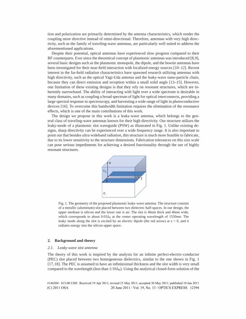
The design we propose in this work is a leaky-wave antenna, which belongs to the gen-eral class of traveling-wave antennas known for their high directivity. Our structure utilizes theleaky-mode of a plasmonic slot waveguide (PSW) as illustrated in Fig. 1. Unlike existing de-signs, sharp directivity can be experienced over a wide frequency range. It is also important topoint out that besides ultra wideband radiation, this structure is much more feasible to fabricate,due to its lower sensitivity to the structure dimensions. Fabrication tolerances on this size scalecan pose serious impediments for achieving a desired functionality through the use of highlyresonant structures.
Fig. 1. The geometry of the proposed plasmonic leaky-wave antenna. The structure consistsof a metallic (aluminum) slot placed between two dielectric half-spaces. In our design, theupper medium is silicon and the lower one is air. The slot is 46nm thick and 46nm wide,which corresponds to about 0.03λ0 at the center operating wavelength of 1550nm. Theleaky mode along the slot is excited by an electric dipole (the red arrow) at z = 0, and itradiates energy into the silicon upper space.
2. Background and theory
2.1. Leaky-wave slot antenna
The theory of this work is inspired by the analysis for an infinite perfect-electric-conductor(PEC) slot placed between two homogeneous dielectrics, similar to the one shown in Fig. 1[17,18]. The PEC is assumed to have an infinitesimal thickness and the slot width is very smallcompared to the wavelength (less than 1/10λ0). Using the analytical closed-form solution of the
#146204 - $15.00 USD Received 19 Apr 2011; revised 23 May 2011; accepted 30 May 2011; published 10 Jun 2011(C) 2011 OSA 20 June 2011 / Vol. 19, No. 13 / OPTICS EXPRESS 12394

Green’s function [19], the asymptotic solutions are calculated to reveal the leaky-wave radiationpattern, which is of a half-conical shape in the dense medium as shown in Fig. 2(a). The energyin the air is negligible compared to silicon. For traveling-wave antennas, the radiation angle θand the beamwidth shown in Fig. 2(b) are determined by the complex propagation constant ofthe traveling wave, which is the leaky slot mode in this case. More specifically, the radiationangle depends on the phase constant β and the beamwidth reflects the leakage constant α .Intuitively, a wider slot leads to a faster leakage, which results in a wider beam.
02.5
57.5
10 −10
−5
0
5
10
0
2.5
5
7.5
y
b)
zx
02.5
57.5
10 −10
−5
0
5
100
2.5
5
7.5
y
a)
z
x
0
2
4
6
8
10
12
14
θ
Fig. 2. The directivity of the PEC slot antenna placed between silicon and air. The schematicof the structure is illustrated in Fig. 1. The simulation is conducted in ADS Momentum byAgilent Technologies based on the method of moments (MoM). The slot antenna operatesat 1550nm. (a) 3D directivity pattern; (b) 2D directivity pattern in the H-plane.
From the phase and leakage constants, the far-field magnetic field can be derived in the H-plane according to Eq. (1) [20].
Hθ = jk2Im0l
η2
e− jk2r
4πrsinθ
(e j
k2l2 (cosθ−K)
) sin(
k2l2 (cosθ −K)
)k2l2 (cosθ −K)
(1)
where Im0 is the equivalent (fictitious) magnetic current in the slot, k2 and η2 refer to the propa-gation constant and the wave impedance of silicon respectively. Moreover, K = (β + jα)/k2 isthe normalized propagation constant of the leaky mode. Quantities l and r represent the lengthof the slot and the observation distance. The H-field in medium 1 (air) is derived using thesame formula and shown to be negligible compared to that in medium 2 (silicon). Finally, theradiation pattern for the power density in the silicon regime is calculated as shown in Eq. (2).
Pθ =12
η2 |Hθ |2 (2)
The interesting feature of this leaky-wave antenna is that the radiation angle is almost fre-quency invariant, because the phase constant β is primarily determined by the relative electricpermittivity of the two dielectric media as described in Eq. (3).
cos(θ) =βk2
≈√
ε1 + ε2
2ε2(3)
This approximation holds true when the slot is very narrow compared to the wavelength. In fact,the wavelength variation affects the leakage constant α more because the slot width changes in
#146204 - $15.00 USD Received 19 Apr 2011; revised 23 May 2011; accepted 30 May 2011; published 10 Jun 2011(C) 2011 OSA 20 June 2011 / Vol. 19, No. 13 / OPTICS EXPRESS 12395
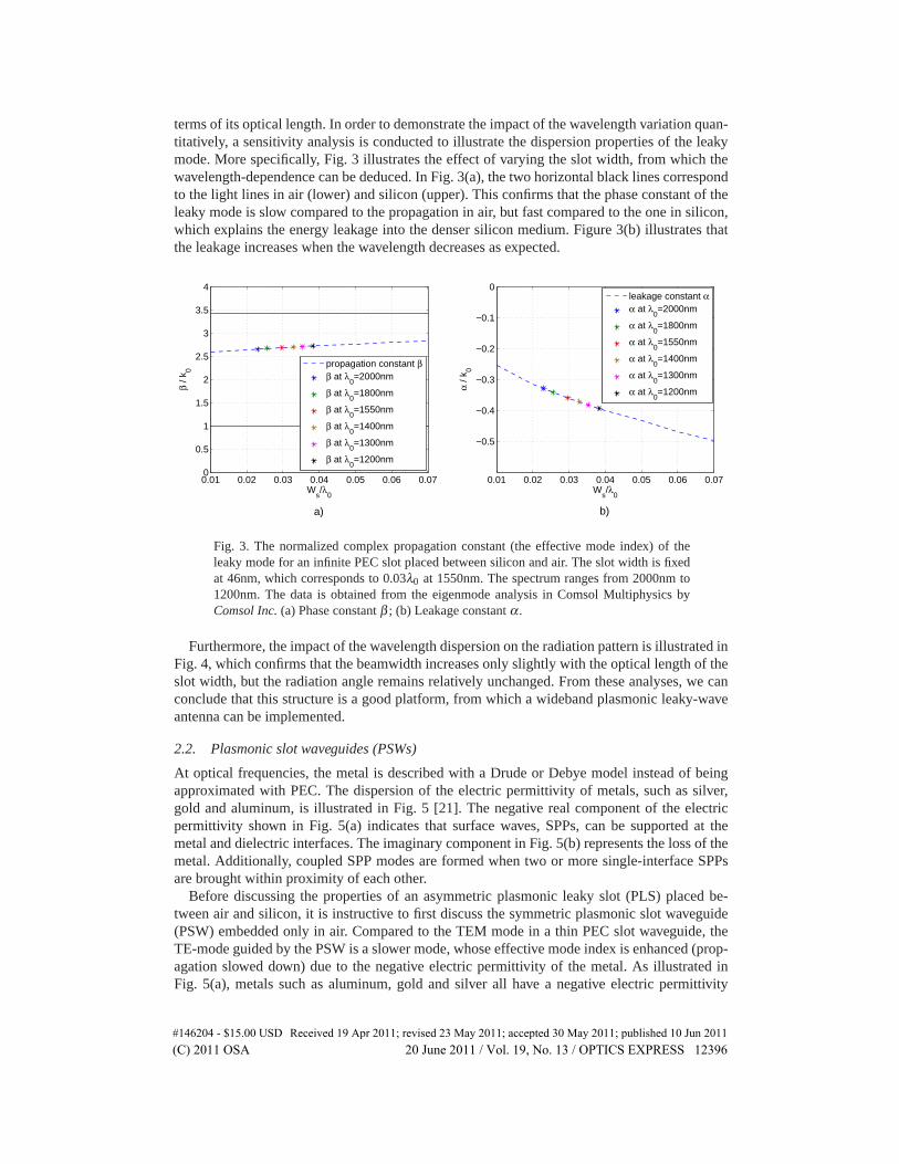
terms of its optical length. In order to demonstrate the impact of the wavelength variation quan-titatively, a sensitivity analysis is conducted to illustrate the dispersion properties of the leakymode. More specifically, Fig. 3 illustrates the effect of varying the slot width, from which thewavelength-dependence can be deduced. In Fig. 3(a), the two horizontal black lines correspondto the light lines in air (lower) and silicon (upper). This confirms that the phase constant of theleaky mode is slow compared to the propagation in air, but fast compared to the one in silicon,which explains the energy leakage into the denser silicon medium. Figure 3(b) illustrates thatthe leakage increases when the wavelength decreases as expected.
0.01 0.02 0.03 0.04 0.05 0.06 0.070
0.5
1
1.5
2
2.5
3
3.5
4
Ws/λ
0
β / k
0
a)
propagation constant ββ at λ
0=2000nm
β at λ0=1800nm
β at λ0=1550nm
β at λ0=1400nm
β at λ0=1300nm
β at λ0=1200nm
0.01 0.02 0.03 0.04 0.05 0.06 0.07
−0.5
−0.4
−0.3
−0.2
−0.1
0
Ws/λ
0
α / k
0
b)
leakage constant αα at λ
0=2000nm
α at λ0=1800nm
α at λ0=1550nm
α at λ0=1400nm
α at λ0=1300nm
α at λ0=1200nm
Fig. 3. The normalized complex propagation constant (the effective mode index) of theleaky mode for an infinite PEC slot placed between silicon and air. The slot width is fixedat 46nm, which corresponds to 0.03λ0 at 1550nm. The spectrum ranges from 2000nm to1200nm. The data is obtained from the eigenmode analysis in Comsol Multiphysics byComsol Inc. (a) Phase constant β ; (b) Leakage constant α .
Furthermore, the impact of the wavelength dispersion on the radiation pattern is illustrated inFig. 4, which confirms that the beamwidth increases only slightly with the optical length of theslot width, but the radiation angle remains relatively unchanged. From these analyses, we canconclude that this structure is a good platform, from which a wideband plasmonic leaky-waveantenna can be implemented.
2.2. Plasmonic slot waveguides (PSWs)
At optical frequencies, the metal is described with a Drude or Debye model instead of beingapproximated with PEC. The dispersion of the electric permittivity of metals, such as silver,gold and aluminum, is illustrated in Fig. 5 [21]. The negative real component of the electricpermittivity shown in Fig. 5(a) indicates that surface waves, SPPs, can be supported at themetal and dielectric interfaces. The imaginary component in Fig. 5(b) represents the loss of themetal. Additionally, coupled SPP modes are formed when two or more single-interface SPPsare brought within proximity of each other.
Before discussing the properties of an asymmetric plasmonic leaky slot (PLS) placed be-tween air and silicon, it is instructive to first discuss the symmetric plasmonic slot waveguide(PSW) embedded only in air. Compared to the TEM mode in a thin PEC slot waveguide, theTE-mode guided by the PSW is a slower mode, whose effective mode index is enhanced (prop-agation slowed down) due to the negative electric permittivity of the metal. As illustrated inFig. 5(a), metals such as aluminum, gold and silver all have a negative electric permittivity
#146204 - $15.00 USD Received 19 Apr 2011; revised 23 May 2011; accepted 30 May 2011; published 10 Jun 2011(C) 2011 OSA 20 June 2011 / Vol. 19, No. 13 / OPTICS EXPRESS 12396

0.5
1
30
210
60
240
90
270
120
300
150
330
180 0
a)
0.5
1
30
210
60
240
90
270
120
300
150
330
180 0
b)
Ws/λ
0 = 0.01
Ws/λ
0 = 0.03
Ws/λ
0 = 0.07
Analytical radiation patternMomentum simulation
Fig. 4. The normalized directivity pattern in the H-plane for an infinite PEC slot placedbetween air and silicon. The results are based on the theoretical calculation using Eq. (2)and the complex propagation constant in Fig. 3. (a) Normalized directivity for the slot widthranging from 0.01λ0 to 0.07λ0; (b) Comparison between the theoretical calculation and theMoM simulation at 1550nm.
500 1000 1500 2000−400
−350
−300
−250
−200
−150
−100
−50
0
50
λ0 (nm)
ε r (re
al)
a)
AgAuAl
500 1000 1500 2000−90
−80
−70
−60
−50
−40
−30
−20
−10
0
λ0 (nm)
ε r (im
agin
ary)
b)
AgAuAl
Fig. 5. The dispersion diagrams of the relative electric permittivity of gold, silver andaluminum at optical frequencies. (a) Real component; (b) Imaginary component.
#146204 - $15.00 USD Received 19 Apr 2011; revised 23 May 2011; accepted 30 May 2011; published 10 Jun 2011(C) 2011 OSA 20 June 2011 / Vol. 19, No. 13 / OPTICS EXPRESS 12397
at optical frequencies. Since the negative εr of aluminum is larger in magnitude compared togold and silver, it behaves closer to a PEC in the optical regime. In other words, the modeguided by an aluminum slot will be slower than that of a PEC slot, but faster than thoseof gold or silver. This can be explained by the fact that the surface mode is known to slowdown significantly close to the spectral region near the transverse resonance condition, where|εmetal |= εdielectric [22,23]. A negative electric permittivity with a larger magnitude in the opti-cal regime implies that the transverse resonance condition takes place at a much shorter wave-length for aluminum compared to gold and silver. Therefore, the fundamental guided mode(a forward even mode) in an aluminum slot propagates closer to the light line in the spectralregime of interest.
The enhancement of the effective mode index could pose challenges in an asymmetric struc-ture, such as our leaky-wave antenna, if the slot mode is slower than the propagation constant inthe dense medium. In such cases the energy will not leak out of the slot mode and hence wouldprohibit radiation. Some versions of PSW on a dielectric substrate that operate at 1550nm witha similar geometry as our PLS have been reported previously [24]. The reason that such designssupport the bound/guided fundamental mode instead of the leaky mode is that silver has beenutilized. To the best of our knowledge, aluminum presents the optimum option for our plas-monic material at optical frequencies in order to facilitate a fast slot mode similar to the one inthe PEC leaky-wave antenna at microwave frequencies.
3. Characteristics of plasmonic leaky slot antennas
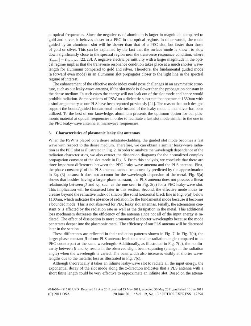
When the PSW is placed on a dense substrate/cladding, the guided slot mode becomes a fastwave with respect to the dense medium. Therefore, we can obtain a similar leaky-wave radia-tion as the PEC slot as illustrated in Fig. 2. In order to analyze the wavelength dependence of theradiation characteristics, we also extract the dispersion diagrams for the normalized complexpropagation constant of the slot mode in Fig. 6. From this analysis, we conclude that there arethree important differences between the PEC leaky-wave antenna and the PLS antenna. First,the phase constant β of the PLS antenna cannot be accurately predicted by the approximationin Eq. (3) because it does not account for the wavelength dispersion of the metal. Fig. 6(a)shows that besides having a larger phase constant, the PLS antenna does not possess a linearrelationship between β and λ0, such as the one seen in Fig. 3(a) for a PEC leaky-wave slot.This implication will be discussed later in this section. Second, the effective mode index in-creases beyond the refractive index of silicon (the solid horizontal black line in Fig. 6(a)) below1100nm, which indicates the absence of radiation for the fundamental mode because it becomesa bounded mode. This is not abserved for PEC leaky slot antennas. Finally, the attenuation con-stant α is affected by the radiation rate as well as the dissipation in the metal. This additionalloss mechanism decreases the efficiency of the antenna since not all of the input energy is ra-diated. The effect of dissipation is more pronounced at shorter wavelengths because the modepenetrates deeper into the plasmonic metal. The efficiency of our PLS antenna will be discussedlater in the section.
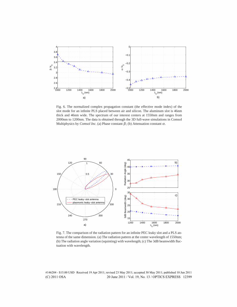
These differences are reflected in their radiation patterns shown in Fig. 7. In Fig. 7(a), thelarger phase constant β of our PLS antenna leads to a smaller radiation angle compared to itsPEC counterpart at the same wavelength. Additionally, as illustrated in Fig. 7(b), the nonlin-earity between β and λ0 results in the observed slight beam-squinting (change in the radiationangle) when the wavelength is varied. The beamwidth also increases visibly at shorter wave-lengths due to the metallic loss as illustrated in Fig. 7(c).
Although theoretically it takes an infinite leaky-wave slot to radiate all the input energy, theexponential decay of the slot mode along the z-direction indicates that a PLS antenna with ashort finite length could be very effective to approximate an infinite slot. Based on the attenu-
#146204 - $15.00 USD Received 19 Apr 2011; revised 23 May 2011; accepted 30 May 2011; published 10 Jun 2011(C) 2011 OSA 20 June 2011 / Vol. 19, No. 13 / OPTICS EXPRESS 12398
1000 1200 1400 1600 1800 20002.4
2.6
2.8
3
3.2
3.4
3.6
3.8
4
λ0 (nm)
β / k
0
a)
1000 1200 1400 1600 1800 2000−0.5
−0.4
−0.3
−0.2
−0.1
0
λ0 (nm)
α / k
0
b)
Fig. 6. The normalized complex propagation constant (the effective mode index) of theslot mode for an infinite PLS placed between air and silicon. The aluminum slot is 46nmthick and 46nm wide. The spectrum of our interest centers at 1550nm and ranges from2000nm to 1200nm. The data is obtained through the 3D full-wave simulations in ComsolMultiphysics by Comsol Inc. (a) Phase constant β ; (b) Attenuation constant α .
0.5
1
30
210
60
240
90
270
120
300
150
330
180 0
a)
25
30
35
40
45
Rad
iatio
n A
ngle
(de
g) b)
1200 1400 1600 1800 2000
15
20
25
30
35
λ0 (nm)
3dB
Bea
mw
idth
(de
g) c)PEC leaky−slot antennaplasmonic leaky−slot antenna
Fig. 7. The comparison of the radiation pattern for an infinite PEC leaky slot and a PLS an-tenna of the same dimension. (a) The radiation pattern at the center wavelength of 1550nm;(b) The radiation angle variation (squinting) with wavelength; (c) The 3dB beamwidth fluc-tuation with wavelength.
#146204 - $15.00 USD Received 19 Apr 2011; revised 23 May 2011; accepted 30 May 2011; published 10 Jun 2011(C) 2011 OSA 20 June 2011 / Vol. 19, No. 13 / OPTICS EXPRESS 12399
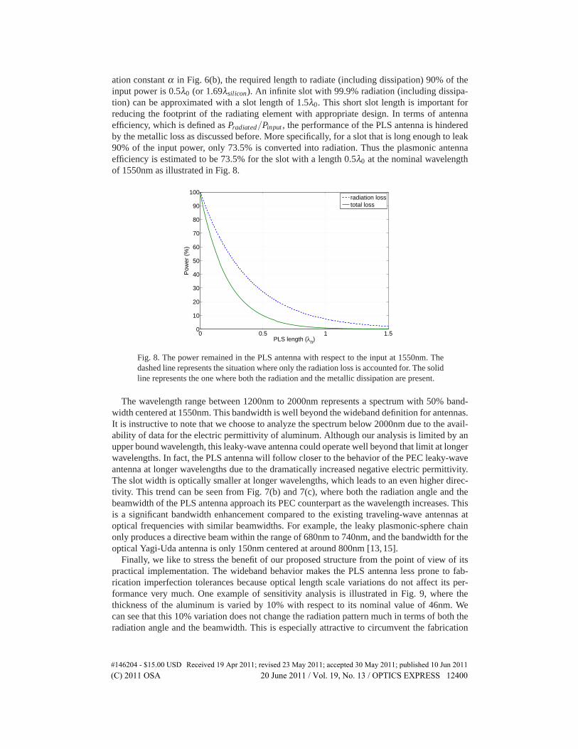
ation constant α in Fig. 6(b), the required length to radiate (including dissipation) 90% of theinput power is 0.5λ0 (or 1.69λsilicon). An infinite slot with 99.9% radiation (including dissipa-tion) can be approximated with a slot length of 1.5λ0. This short slot length is important forreducing the footprint of the radiating element with appropriate design. In terms of antennaefficiency, which is defined as Pradiated/Pinput , the performance of the PLS antenna is hinderedby the metallic loss as discussed before. More specifically, for a slot that is long enough to leak90% of the input power, only 73.5% is converted into radiation. Thus the plasmonic antennaefficiency is estimated to be 73.5% for the slot with a length 0.5λ0 at the nominal wavelengthof 1550nm as illustrated in Fig. 8.
0 0.5 1 1.50
10
20
30
40
50
60
70
80
90
100
PLS length (λ0)
Pow
er (
%)
radiation losstotal loss
Fig. 8. The power remained in the PLS antenna with respect to the input at 1550nm. Thedashed line represents the situation where only the radiation loss is accounted for. The solidline represents the one where both the radiation and the metallic dissipation are present.
The wavelength range between 1200nm to 2000nm represents a spectrum with 50% band-width centered at 1550nm. This bandwidth is well beyond the wideband definition for antennas.It is instructive to note that we choose to analyze the spectrum below 2000nm due to the avail-ability of data for the electric permittivity of aluminum. Although our analysis is limited by anupper bound wavelength, this leaky-wave antenna could operate well beyond that limit at longerwavelengths. In fact, the PLS antenna will follow closer to the behavior of the PEC leaky-waveantenna at longer wavelengths due to the dramatically increased negative electric permittivity.The slot width is optically smaller at longer wavelengths, which leads to an even higher direc-tivity. This trend can be seen from Fig. 7(b) and 7(c), where both the radiation angle and thebeamwidth of the PLS antenna approach its PEC counterpart as the wavelength increases. Thisis a significant bandwidth enhancement compared to the existing traveling-wave antennas atoptical frequencies with similar beamwidths. For example, the leaky plasmonic-sphere chainonly produces a directive beam within the range of 680nm to 740nm, and the bandwidth for theoptical Yagi-Uda antenna is only 150nm centered at around 800nm [13,15].
Finally, we like to stress the benefit of our proposed structure from the point of view of itspractical implementation. The wideband behavior makes the PLS antenna less prone to fab-rication imperfection tolerances because optical length scale variations do not affect its per-formance very much. One example of sensitivity analysis is illustrated in Fig. 9, where thethickness of the aluminum is varied by 10% with respect to its nominal value of 46nm. Wecan see that this 10% variation does not change the radiation pattern much in terms of both theradiation angle and the beamwidth. This is especially attractive to circumvent the fabrication
#146204 - $15.00 USD Received 19 Apr 2011; revised 23 May 2011; accepted 30 May 2011; published 10 Jun 2011(C) 2011 OSA 20 June 2011 / Vol. 19, No. 13 / OPTICS EXPRESS 12400

tolerance of nano-scale features.
0.2
0.4
0.6
0.8
1
30
210
60
240
90
270
120
300
150
330
180 0
41nm46nm51nm
Fig. 9. The effect of 10% variation in the aluminum film thickness on the radiation patternat 1550nm.
In summary, the PLS antenna that operates at 1550nm produces a radiation angle of 32o
and a 3dB beamwidth of 23.8o. The range of deviation in the radiation angle and the 3dBbeamwidth are [−4.4o,1.8o] and [+9.8o,−3.3o] when the wavelength varies from 1200nm to2000nm respectively. At 1550nm, the estimated antenna efficiency is 73.5% for a slot length of0.5λ0.
4. Conclusion
In conclusion, we present a leaky-wave slot antenna at optical frequencies that achieves a wide-band operation, which is centered at 1550nm with a 50% bandwidth that ranges from 2000nmto 1200nm. Compared to existing optical antennas that rely on resonant structures, our designconsists of a simple sub-wavelength (in width and thickness) aluminum slot placed on silicon.The absence of any resonant elements gives rise to a wideband behavior, which is insensitiveto small fabrication tolerances. It is also observed that due to the dispersion of the electricpermittivity of aluminum at optical frequencies, the leaky-mode of our slot antenna has a lowerbound limit at 1100nm, below which the leaky mode becomes a bounded mode. This is notobserved for PEC leaky slot antennas. The radiation pattern of the PLS antenna approachesthe one of its PEC counterpart with increasing wavelength. Although our analysis is performedfor the spectrum from 2000nm to 1200nm, the PLS antenna is expected to operate at longerwavelengths with an even more directive far-field radiation pattern. Furthermore, this designcan be extended by placing an array of slots side-by-side (along the y-axis in Fig. 1) to increasethe directivity in the E-plane (the xy-plane). In this way, the half-conical beam shape of Fig. 2can be transformed into a pencil beam if so desired. We foresee these proposed widebandleaky-wave antennas or arrays to be very useful for the efficient conversion of localized energyin subwavelength dimensions to free space.
#146204 - $15.00 USD Received 19 Apr 2011; revised 23 May 2011; accepted 30 May 2011; published 10 Jun 2011(C) 2011 OSA 20 June 2011 / Vol. 19, No. 13 / OPTICS EXPRESS 12401