INTERFÉRENCES ET DIFFRACTION Interférences et diffraction ...
Upload
shyue-ping-ongCategory
view
1.544download
0
Other diffraction techniques and common crystal structures of real materials
Shyue Ping OngDepartment of NanoEngineeringUniversity of California, San Diego

Other diffraction techniques¡ XRD is the most common (and typically most economical)
means of determining crystal structures.
¡ Electrons and neutrons are also widely used scattering techniques.¡ Employs wave-particle duality of electrons and neutrons¡ Transmission electron microscopes (TEM) are more expensive than
XRD equipment, but still common¡ Neutron diffraction is typically performed at national and
international reactor facilities
NANO 106 - Crystallography of Materials by Shyue Ping Ong - Lecture 13
2

Comparison of different diffraction techniques
X-rays
λ ~ 0.1nm
Uncharged
No magnetic dipole
Scattered by atomic charge densities
(~0.1nm)
Electrons
λ ~ 0.002nm
Charged
Possesses magnetic dipole
Scattered by electronic and nuclear charge densities (~0.1nm)
Neutrons
λ ~ 0.1nm
Uncharged
Possess magnetic dipole
Scattered by atomic nucleus (~0.0001nm)
NANO 106 - Crystallography of Materials by Shyue Ping Ong - Lecture 13
3
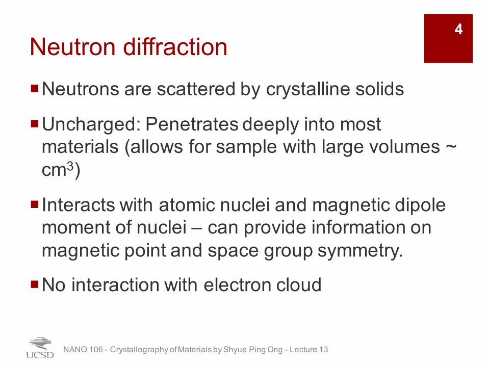
Neutron diffraction¡Neutrons are scattered by crystalline solids
¡Uncharged: Penetrates deeply into most materials (allows for sample with large volumes ~ cm3)
¡ Interacts with atomic nuclei and magnetic dipole moment of nuclei – can provide information on magnetic point and space group symmetry.
¡No interaction with electron cloud
NANO 106 - Crystallography of Materials by Shyue Ping Ong - Lecture 13
4

Applications of Neutron Scattering¡ Elastic nuclear scattering (Bragg scattering)
¡ Ability to locate light atomic species in presence of heavy atoms (no simple dependence on Z)
¡ Elastic magnetic scattering¡ Probe magnetic structure
¡ Inelastic scattering¡ Interaction of low-energy neutrons with vibrating crystal lattice and spin waves¡ Probe magnetic phase transitions
¡ Isotopic substitution¡ Isotopes can have different neutron scattering¡ Tailor scattering factors to be more or less sensitive to a particular element
NANO 106 - Crystallography of Materials by Shyue Ping Ong - Lecture 13
5
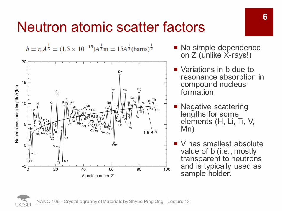
Neutron atomic scatter factors¡ No simple dependence
on Z (unlike X-rays!)
¡ Variations in b due to resonance absorption in compound nucleus formation
¡ Negative scattering lengths for some elements (H, Li, Ti, V, Mn)
¡ V has smallest absolute value of b (i.e., mostly transparent to neutrons and is typically used as sample holder.
NANO 106 - Crystallography of Materials by Shyue Ping Ong - Lecture 13
6

Comparison of different diffraction techniques
X-rays
λ ~ 0.1nm
Uncharged
No magnetic dipole
Scattered by atomic charge densities
(~0.1nm)
Electrons
λ ~ 0.002nm
Charged
Possesses magnetic dipole
Scattered by electronic and nuclear charge densities (~0.1nm)
Neutrons
λ ~ 0.1nm
Uncharged
Possess magnetic dipole
Scattered by atomic nucleus (~0.0001nm)
NANO 106 - Crystallography of Materials by Shyue Ping Ong - Lecture 13
7
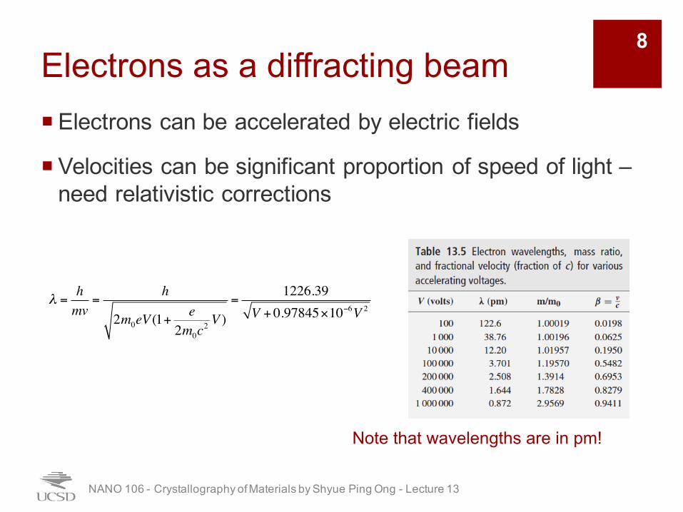
Electrons as a diffracting beam¡ Electrons can be accelerated by electric fields
¡ Velocities can be significant proportion of speed of light –need relativistic corrections
NANO 106 - Crystallography of Materials by Shyue Ping Ong - Lecture 13
λ =hmv
=h
2m0eV (1+e
2m0c2 V )
=1226.39
V + 0.97845×10⁻⁶V 2
Note that wavelengths are in pm!
8

Interaction of electrons with crystal lattices¡ Strong interactions with both electron clouds and positively charged
nuclei
¡ Probability of scattering of electron beam is ~ four times higher than for X-rays
¡ Electron scattering factor can be related to the X-ray scattering factor by the Moth-Bethe formula:
¡ High probability of scattering leads to multiple scattering events (dynamic scattering) è electron scattering must be treated with dynamic scattering theory
NANO 106 - Crystallography of Materials by Shyue Ping Ong - Lecture 13
f el (s) =e
16π 2ε0 s2 [Z − f X (s)] where s = sinθ
λ
9

Electron diffraction geometry¡ Wavelengths for electrons are much smaller¡ Diffraction angles are much smaller (typically on the order of milliradians)¡ Bragg condition can be approximated by
¡ Need to only look close to incident beam to find diffracted beam¡ Ewald spheres are ~ 100-1000 times larger than X-rays (possible to orient
crystal such that whole plane of reciprocal lattice points are tangent to sphere)
NANO 106 - Crystallography of Materials by Shyue Ping Ong - Lecture 13
2dhklθ = λ
10

Sample preparation¡ Strong interaction necessitates the use of very thin or
small samples (~ few hundred nm)
¡ Unlike neutrons and X-rays, electrons are absorbed by matter
¡ Implications:¡ Sample preparation is time-consuming and difficult¡ Infinite crystal assumption is no longer valid and reciprocal lattice
points can no longer be treated as zero-volume mathematical points (reciprocal point shape is the reciprocal of the extent of crystal – for thin films, this means a cylinder extended in direction of thin film)
¡ Reciprocal point volume can intersect Ewald sphere even when actual point is not on Ewald sphere – increases probability of diffraction
NANO 106 - Crystallography of Materials by Shyue Ping Ong - Lecture 13
11

Transmission electron microscope (TEM)
NANO 106 - Crystallography of Materials by Shyue Ping Ong - Lecture 13
Heating W filament emits electrons
Focuses and directs electron beam using magnetic fields
Main image forming lens
Fairly large- Can be > 3 stories
high!- Vacuum is maintained
as electrons cannot travel very far in air
12

Synchrontron X-ray sources¡ X-rays produced by circular motion of charged particles,
e.g. electrons (recall that X-rays are produced by acceleration of charged particles)
¡ Properties¡ High beam intensity: continuous source with five or more orders of
magnitude higher intensities than X-ray tubes¡ Broad radiation spectrum¡ Strong polarization: Nearly 100% linearly polarized, circular or
elliptical polarizations possible
NANO 106 - Crystallography of Materials by Shyue Ping Ong - Lecture 13
13

Example applications of SynchrotonXRD
¡ In-situ study of crystallization with heating¡ High-flux allows for diffraction patterns to be taken in short
amount of time
¡Study of superlattice orderings, e.g., ordered α’-FeCo¡ Superlattice reflections can be several orders of magnitude
less intense than fundamental reflections
NANO 106 - Crystallography of Materials by Shyue Ping Ong - Lecture 13
14

Common crystal structures
NANO 106 - Crystallography of Materials by Shyue Ping Ong - Lecture 13
15
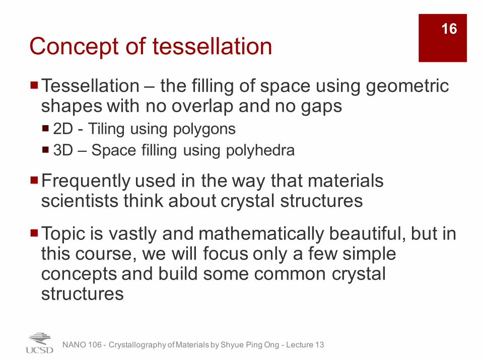
Concept of tessellation¡Tessellation – the filling of space using geometric
shapes with no overlap and no gaps¡ 2D - Tiling using polygons¡ 3D – Space filling using polyhedra
¡Frequently used in the way that materials scientists think about crystal structures
¡Topic is vastly and mathematically beautiful, but in this course, we will focus only a few simple concepts and build some common crystal structures
NANO 106 - Crystallography of Materials by Shyue Ping Ong - Lecture 13
16

Regular polygons and polyhedra¡Regular polygons and polyhedra have identical sides
and angles.¡2D¡ Equilateral triangle¡ Square¡ Regular hexagon
¡3D (also known as platonic solids)¡ Tetrahedron¡ Cube¡ Octahedron¡ Icosahedron¡ Pentagonal dodecahedron
NANO 106 - Crystallography of Materials by Shyue Ping Ong - Lecture 13
17
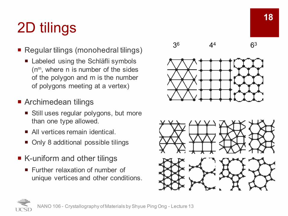
2D tilings¡ Regular tilings (monohedral tilings)
¡ Labeled using the Schläfli symbols (nm, where n is number of the sides of the polygon and m is the number of polygons meeting at a vertex)
¡ Archimedean tilings¡ Still uses regular polygons, but more
than one type allowed.¡ All vertices remain identical.¡ Only 8 additional possible tilings
¡ K-uniform and other tilings¡ Further relaxation of number of
unique vertices and other conditions.
NANO 106 - Crystallography of Materials by Shyue Ping Ong - Lecture 13
36 44 63
18

Stackings of 36 tilings¡ 3D crystals can be constructed by stackings of 2D tilings.
¡ An important class of structures – the closed-packed structures – comprise of stacking of 36 tilings
NANO 106 - Crystallography of Materials by Shyue Ping Ong - Lecture 13
• A 36 tiling has plane group p6mm• If we consider a single layer of atoms
occupying “A” sites, two kinds of interstitial sites are created – “B” sites and “C” sites.
• Subsequent layers can occupy either B or C sites to form close-packed structures, and the process can be repeated to generate infinite variations of stacking
19

Two common forms of closed packing¡ Hexagonal close-packed¡ ABAB stacking
¡ Face-centered cubic¡ ABCABC stacking
NANO 106 - Crystallography of Materials by Shyue Ping Ong - Lecture 13
Fcc perspective views
20

Interstitials in close-packed structures¡ Tetrahedral interstitial
¡ Four-fold coordinated¡ Formed by having an atom atop three atoms
¡ Octahedral interstitial¡ Formed when there are no atoms sitting directly on top of
the interstitial¡ Six-fold coordinated¡ Larger than tetrahedral site¡ Interstitial can be labeled as α, β, or γ depending on
whether the site is formed by B-C, A-C or A-B planes respectively.
¡ (Recall that NaCl can be thought of as having an fcc lattice of Na with Cl sitting in the oct interstitial)
NANO 106 - Crystallography of Materials by Shyue Ping Ong - Lecture 13
21
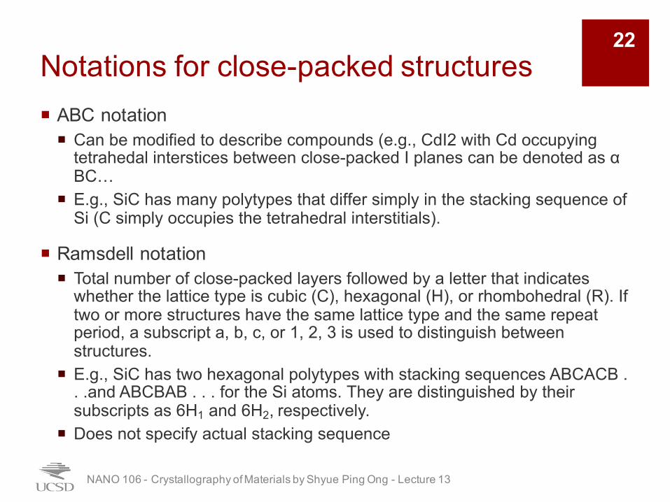
Notations for close-packed structures¡ ABC notation¡ Can be modified to describe compounds (e.g., CdI2 with Cd occupying
tetrahedal interstices between close-packed I planes can be denoted as α BC…
¡ E.g., SiC has many polytypes that differ simply in the stacking sequence of Si (C simply occupies the tetrahedral interstitials).
¡ Ramsdell notation¡ Total number of close-packed layers followed by a letter that indicates
whether the lattice type is cubic (C), hexagonal (H), or rhombohedral (R). If two or more structures have the same lattice type and the same repeat period, a subscript a, b, c, or 1, 2, 3 is used to distinguish between structures.
¡ E.g., SiC has two hexagonal polytypes with stacking sequences ABCACB . . .and ABCBAB . . . for the Si atoms. They are distinguished by their subscripts as 6H1 and 6H2, respectively.
¡ Does not specify actual stacking sequence
NANO 106 - Crystallography of Materials by Shyue Ping Ong - Lecture 13
22

Crystal structures of elements
NANO 106 - Crystallography of Materials by Shyue Ping Ong - Lecture 13
23

Parent, derivative and superlatticestructures
¡Derivative structures are those that are derived from simpler structures by substitution of one atom for another
¡ Interstitial structures are obtained by ordered occupation of subsets of interstitial sites in simple structures
NANO 106 - Crystallography of Materials by Shyue Ping Ong - Lecture 13
24

Definition of Superlattice¡ Consider two lattice’s whose basis vectors are related by:
¡ If Mij are integers and det(M) = 1, then the two lattices coincide.¡ If Mij are integers and det(M) > 1, then the lattice defined by A’ is a
superlattice of that defined by A.¡ If Mij are integers and det(M) < 1, then the lattice defined by A’ is a
sublattice of that defined by A.
NANO 106 - Crystallography of Materials by Shyue Ping Ong - Lecture 13
!A =
a1!
a2!
a3!
"
#
$$$$$
%
&
'''''
=
M11 M12 M13
M21 M22 M23
M31 M32 M33
"
#
$$$$
%
&
''''
a1a2a3
"
#
$$$$
%
&
''''=MA
25

Classification of structures¡ Strukturbericht symbols¡ Letter followed by number¡ Sequential numbering by order of
discovery, e.g., A2 refers to bcc structure.¡ Frequently used in materials science
literature
¡Pearson symbol¡ Bravais lattice symbol (a, m, o, t, h,
c) + centering (P, C, I, F) + # of atoms in unit cell.
¡ E.g., NaCl has Pearson symbol cF8.
¡ Not unique.
NANO 106 - Crystallography of Materials by Shyue Ping Ong - Lecture 13
26

Structure of metals¡ Derivative structures are based on fcc, bcc, and hcp
parent structures¡ fcc (A1) and hcp (A3) – Stackings of 36 tiles.¡ bcc (A2) – Stacking of 44 tiles.¡ fcc and bcc are derivatives of the simple cubic structure, which is
rarely observed for elements (though common in compounds) ¡ fcc and hcp are close-packed – packing fraction of 74.05%. bcc is
not close-packed – packing fraction of 68.02%.
NANO 106 - Crystallography of Materials by Shyue Ping Ong - Lecture 13
27
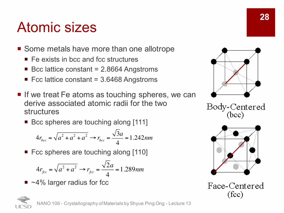
Atomic sizes¡ Some metals have more than one allotrope¡ Fe exists in bcc and fcc structures¡ Bcc lattice constant = 2.8664 Angstroms¡ Fcc lattice constant = 3.6468 Angstroms
¡ If we treat Fe atoms as touching spheres, we can derive associated atomic radii for the two structures¡ Bcc spheres are touching along [111]
¡ Fcc spheres are touching along [110]
¡ ~4% larger radius for fcc
NANO 106 - Crystallography of Materials by Shyue Ping Ong - Lecture 13
4rbcc = a2 + a2 + a2 → rbcc =3a4
=1.242nm
4rfcc = a2 + a2 → rfcc =2a4
=1.289nm
28
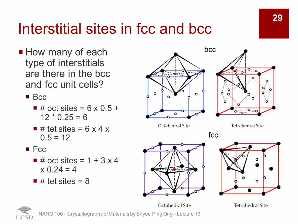
Interstitial sites in fcc and bcc¡ How many of each
type of interstitials are there in the bcc and fcc unit cells?¡ Bcc¡ # oct sites = 6 x 0.5 +
12 * 0.25 = 6¡ # tet sites = 6 x 4 x
0.5 = 12¡ Fcc¡ # oct sites = 1 + 3 x 4
x 0.24 = 4¡ # tet sites = 8
NANO 106 - Crystallography of Materials by Shyue Ping Ong - Lecture 13
bcc
fcc
29

Packing fractions¡ Ratio of the volume occupied by atoms to the total volume of
unit cell
¡ Kepler’s conjecture: No arrangement of equally sized spheres filling space has a greater average density than that of the cubic close packing (face-centered cubic) and hexagonal close packing arrangements – recently proved with help of computers by Thomas Hale
NANO 106 - Crystallography of Materials by Shyue Ping Ong - Lecture 13
pfcc =4× 43πrfcc
3
a3= 74.05%
pbcc =2× 43πrbcc
3
a3= 68.02%
30

Alloys¡ Substitutional solid solutions¡ Same crystal structure as components¡ Lattice constant governed by Vegard’s law (with some deviations)
¡ Interstitial alloys¡ One component atom sits in interstitial sites of another large
component atom¡ Lattice constant determined by strain effects
NANO 106 - Crystallography of Materials by Shyue Ping Ong - Lecture 13
31

Hume-Rothery rules1. Atomic size factor: The range of solid solubility will be restricted if
the atomic radii differ by more than about 15%.
2. Electronegativity valency effect: Large electronegativity differences between components of a binary alloy can promote charge transfer and differences in the covalency, ionicity, or metallicity of the bonds. This leads to bond energy differences between A−A, A−B, and B−B bond energies in the alloy. A strong proclivity for A−B bond formation can lead to the formation of stable compounds.
3. Relative valency effect: A metal of lower valency is more likely to dissolve in a metal of higher valency than vice versa. This rule is not universally obeyed.
NANO 106 - Crystallography of Materials by Shyue Ping Ong - Lecture 13
32

Derivative and superlattice structures in alloys¡ At high temperatures, alloys are typically disordered. As temperature
is decreased, some alloys undergo a disorder-order phase transition resulting in an ordered solid solution or superlattice or superstructure.
¡ fcc (Fm-3m) derivatives:
NANO 106 - Crystallography of Materials by Shyue Ping Ong - Lecture 13
L10: CuAu, FePt, FePd L12: Cu3Au, Au3Cd, AlCo3
Tetragonal P4/mmm Cubic Pm-3m
33

XRD patterns
NANO 106 - Crystallography of Materials by Shyue Ping Ong - Lecture 13
34

Fcc- interstitial substitution¡Diamond cubic (A4)¡ Tet interstial in fcc occupied¡ Common for many Group IV
semiconductors (Si, Ge)
¡Rocksalt (B1)¡ Oct interstitial occupied by a different
atom¡ Common for many ionic compounds
(NaCl, LiF, etc.)
NANO 106 - Crystallography of Materials by Shyue Ping Ong - Lecture 13
35
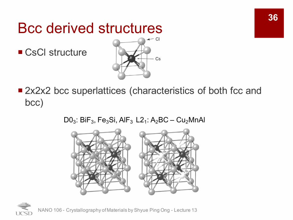
Bcc derived structures¡ CsCl structure
¡ 2x2x2 bcc superlattices (characteristics of both fcc and bcc)
NANO 106 - Crystallography of Materials by Shyue Ping Ong - Lecture 13
D03: BiF3, Fe3Si, AlF3 L21: A2BC – Cu2MnAl
36

Diamond cubic derived structures
¡Zincblende (B3)¡ III-V and II-VI compounds¡ ZnS, AsGa, InSb
¡Fluorite – AB2 (C)¡ CaF2
¡Anti-fluorite¡ Similar to fluorite, but with
cations and anions reversed¡ K2O
NANO 106 - Crystallography of Materials by Shyue Ping Ong - Lecture 13
37

Hcp derived structures¡ Interstitial occupation in
tet or oct sites¡ Wurtzite ZnO (B4) structure
– occupation of one of tetsites in hcp
¡ B81 NiAs structure –occupation of oct sites
NANO 106 - Crystallography of Materials by Shyue Ping Ong - Lecture 13
38
Types of ceramics¡ Restrict our discussion to binary ceramics (two
components)
¡ Ionic ceramics¡ Compounds of an electropositive cation M with an electronegative
anion X, e.g., Al2O3, MgO, ZrO2, NaCl¡ Packing and coordination governed by Pauling’s rules as discussed
earlier in the course
¡ Covalent ceramics¡ Covalent bonding¡ Examples: GaAs, SiC, ZnO, SiO2
¡ Note that the ionic/covalent classification is not a strict one – all structures have some ionic and covalent character
NANO 106 - Crystallography of Materials by Shyue Ping Ong - Lecture 13
39
Halide salts¡ Monovalent cations and anions
¡ Two main types of structure¡ Rocksalt or NaCl structure (fcc derivative)¡ CsCl structure (bcc derivative)
¡ Significantly larger radius of Cs compared to Na responsible for the difference in structures
¡ CsCl in fact exists in both the α-CsCl form, as well as a rocksalt structure at higher temperatures
NANO 106 - Crystallography of Materials by Shyue Ping Ong - Lecture 13
40

Oxides of Fe¡FeO (wustite)¡ Rocksalt (NaCl) structure
¡Fe3O4 (Magnetite)¡ Spinel structure
¡Fe2O3¡ α (hematite)¡ γ (maghemite)¡ β and δ are two other allotropes
NANO 106 - Crystallography of Materials by Shyue Ping Ong - Lecture 13
41

Close-packed sulfides and oxides
¡Zincblende ZnS structure discussed previously
¡Corundum Al2O3¡ Mineral name for ruby / emerald / sapphire¡ Almost hcp O2- with Al3+ occupying 2/3 of oct sites
NANO 106 - Crystallography of Materials by Shyue Ping Ong - Lecture 13
42

Ternary oxide structures¡ Perovskite ABO3 (E21)¡ Prototype CaTiO3
¡ Large family of crystalline ceramics¡ Idealized perovskite is cubic, but more typically is tetragonal or
orthorhombic due to tilting or distortion¡ Many technological applications rely on perovskite structures¡ Solar¡ Ferroelectrics¡ Catalysts¡ Superconductors¡ ….
NANO 106 - Crystallography of Materials by Shyue Ping Ong - Lecture 13
43

Ternary oxide structures¡Spinel AB2O4¡ Prototype MgAl2O4
¡ Fcc sublattice of O2-, with A occupying a fraction of tetsites and B occupying a fraction of oct sites.
NANO 106 - Crystallography of Materials by Shyue Ping Ong - Lecture 13
44