Two ADCs, One DAC, Low Power Codec with Audio DSPs · 2019-08-06 · Two ADCs, One DAC, Low Power...
226
Two ADCs, One DAC, Low Power Codec with Audio DSPs Data Sheet ADAU1788 Rev. 0 Document Feedback Information furnished by Analog Devices is believed to be accurate and reliable. However, no responsibility is assumed by Analog Devices for its use, nor for any infringements of patents or other rights of third parties that may result from its use. Specifications subject to change without notice. No license is granted by implication or otherwise under any patent or patent rights of Analog Devices. Trademarks and registered trademarks are the property of their respective owners. One Technology Way, P.O. Box 9106, Norwood, MA 02062-9106, U.S.A. Tel: 781.329.4700 ©2019 Analog Devices, Inc. All rights reserved. Technical Support www.analog.com FEATURES Programmable FastDSP audio processing engine Up to 768 kHz sample rate Biquad filters, limiters, volume controls, mixing 28-bit SigmaDSP audio processing core Visually programmable using SigmaStudio Up to 50 MIPS performance Low latency, 24-bit ADCs and DAC 96 dB SNR (signal through PGA and ADC with A-weighted filter) 105 dB combined SNR (signal through DAC and headphone with A-weighted filter) Serial port fSYNC frequency from 8 kHz to 768 kHz 5 μs group delay (fS = 768 kHz) analog in to analog out 2 single-ended analog inputs, configurable as microphone or line inputs 4 digital microphone inputs 1 analog differential audio output, configurable as either line output or headphone driver PLL supporting any input clock rate from 30 kHz to 27 MHz Full-duplex, 4-channel ASRCs 16-channel serial audio port supporting I 2 S, left justified, or up to TDM16 8 interpolators and 8 decimators with flexible routing Power supplies Analog AVDD at 1.8 V typical Digital I/O IOVDD at 1.1 V to 1.98 V Digital DVDD at 0.9 V typical Low power (8.030 mW for typical power consumption) I 2 C and SPI control interfaces Flexible GPIO 42-ball, 0.35 mm pitch, 2.695 mm × 2.320 mm WLCSP APPLICATIONS Noise cancelling handsets, headsets, and headphones Bluetooth ANC handsets, headsets, and headphones Personal navigation devices Digital still and video cameras Musical instrument effect processors Multimedia speaker systems Smartphones GENERAL DESCRIPTION The ADAU1788 is a codec with two inputs and one output that incorporates two digital signal processors (DSPs). The path from the analog input to the DSP core to the analog output is optimized for low latency and is ideal for noise cancelling headsets. With the addition of just a few passive components, the ADAU1788 provides a noise cancelling headphone solution. Note that throughout this data sheet, multifunction pins, such as BCLK_0/MP1, are referred to either by the entire pin name or by a single function of the pin, for example, BCLK_0, when only that function is relevant.
Transcript of Two ADCs, One DAC, Low Power Codec with Audio DSPs · 2019-08-06 · Two ADCs, One DAC, Low Power...

Two ADCs, One DAC, Low Power Codec with Audio DSPs
Data Sheet ADAU1788
Rev. 0 Document Feedback Information furnished by Analog Devices is believed to be accurate and reliable. However, no responsibility is assumed by Analog Devices for its use, nor for any infringements of patents or other rights of third parties that may result from its use. Specifications subject to change without notice. No license is granted by implication or otherwise under any patent or patent rights of Analog Devices. Trademarks and registered trademarks are the property of their respective owners.
One Technology Way, P.O. Box 9106, Norwood, MA 02062-9106, U.S.A. Tel: 781.329.4700 ©2019 Analog Devices, Inc. All rights reserved. Technical Support www.analog.com
FEATURES Programmable FastDSP audio processing engine
Up to 768 kHz sample rate Biquad filters, limiters, volume controls, mixing
28-bit SigmaDSP audio processing core Visually programmable using SigmaStudio Up to 50 MIPS performance
Low latency, 24-bit ADCs and DAC 96 dB SNR (signal through PGA and ADC with
A-weighted filter) 105 dB combined SNR (signal through DAC and headphone
with A-weighted filter) Serial port fSYNC frequency from 8 kHz to 768 kHz 5 μs group delay (fS = 768 kHz) analog in to analog out 2 single-ended analog inputs, configurable as microphone
or line inputs 4 digital microphone inputs 1 analog differential audio output, configurable as either
line output or headphone driver PLL supporting any input clock rate from 30 kHz to 27 MHz Full-duplex, 4-channel ASRCs 16-channel serial audio port supporting I2S, left justified, or
up to TDM16 8 interpolators and 8 decimators with flexible routing Power supplies
Analog AVDD at 1.8 V typical Digital I/O IOVDD at 1.1 V to 1.98 V Digital DVDD at 0.9 V typical
Low power (8.030 mW for typical power consumption) I2C and SPI control interfaces Flexible GPIO 42-ball, 0.35 mm pitch, 2.695 mm × 2.320 mm WLCSP
APPLICATIONS Noise cancelling handsets, headsets, and headphones Bluetooth ANC handsets, headsets, and headphones Personal navigation devices Digital still and video cameras Musical instrument effect processors Multimedia speaker systems Smartphones
GENERAL DESCRIPTION The ADAU1788 is a codec with two inputs and one output that incorporates two digital signal processors (DSPs). The path from the analog input to the DSP core to the analog output is optimized for low latency and is ideal for noise cancelling headsets. With the addition of just a few passive components, the ADAU1788 provides a noise cancelling headphone solution.
Note that throughout this data sheet, multifunction pins, such as BCLK_0/MP1, are referred to either by the entire pin name or by a single function of the pin, for example, BCLK_0, when only that function is relevant.

ADAU1788 Data Sheet
Rev. 0 | Page 2 of 226
TABLE OF CONTENTS Features .............................................................................................. 1 Applications ....................................................................................... 1 General Description ......................................................................... 1 Revision History ............................................................................... 5 Functional Block Diagram .............................................................. 6 Specifications ..................................................................................... 7
Analog Performance Specifications ........................................... 7 Crystal Amplifier Specifications ................................................. 9 Digital Input and Output Specifications ................................... 9 Power Supply Specifications...................................................... 10 Power-Down Current ................................................................ 10 Typical Power Consumption..................................................... 11 Digital Filters ............................................................................... 12 Digital Timing Specifications ................................................... 13
Absolute Maximum Ratings .......................................................... 17 Thermal Resistance .................................................................... 17 ESD Caution ................................................................................ 17
Pin Configuration and Function Descriptions ........................... 18 Typical Performance Characteristics ........................................... 21 System Block Diagram ................................................................... 28 Theory of Operation ...................................................................... 29 System Clocking and Power-Up ................................................... 30
Power-Down Operation and Options ..................................... 30 Example ADC to DAC Power-up ............................................. 31 DVDD LDO Regulator .............................................................. 31 Clock Initialization ..................................................................... 31 PLL................................................................................................ 32 Multichip Phase Synchronization ............................................ 33 Clock Output ............................................................................... 33 Power Supply Sequencing ......................................................... 33
Signal Routing ................................................................................. 34 Input Signal Paths ........................................................................... 35
Analog Inputs .............................................................................. 35 Digital Microphone Inputs ........................................................ 36 ADCs ............................................................................................ 37
Output Signal Paths ........................................................................ 38 Analog Outputs........................................................................... 38 DAC .............................................................................................. 38
PDM Outputs .............................................................................. 39 ASRCs .......................................................................................... 39 Interpolation and Decimation Blocks ..................................... 40 Signal Levels ................................................................................ 40
FastDSP Core .................................................................................. 41 Instructions ................................................................................. 41 Filter Precision ............................................................................ 41 Flags and Conditional Execution ............................................. 41 Input Sources .............................................................................. 41 Power and Run Control ............................................................. 42 Data Memory .............................................................................. 42 Parameters ................................................................................... 42 Parameter Bank Switching ........................................................ 42 Parameter Bank Copying .......................................................... 42 Parameter Memory Access ........................................................ 43 FastDSP Parameter Safeload ..................................................... 43
SigmaDSP Core ............................................................................... 44 Signal Processing Details ........................................................... 44 Read/Write Data Formats ......................................................... 45 Software Safeload ....................................................................... 46 FastDSP Safeload ........................................................................ 46
Program RAM, Parameter RAM, and Data RAM ..................... 47 Program RAM ............................................................................ 47 Parameter RAM .......................................................................... 47 Data RAM ................................................................................... 47
Power Saving Options .................................................................... 48 ADC Bias Current Control ....................................................... 48 DAC Bias Current Control ........................................................ 48 DAC Low Power Modes ............................................................ 48 PLL Bypass .................................................................................. 48 SigmaDSP Clock Speed Control............................................... 49 Asynchronous Sample Rate Converters Low Power Modes. 49
Control Port .................................................................................... 50 Burst Mode Communication .................................................... 50 Reading and Writing to Memories .......................................... 51 I2C Port ........................................................................................ 51 SPI Port ........................................................................................ 54 Multipurpose Pins ...................................................................... 55

Data Sheet ADAU1788
Rev. 0 | Page 3 of 226
Serial Data Port ................................................................................ 56 Applications Information ............................................................... 58
Power Supply Bypass Capacitors ............................................... 58 Layout ........................................................................................... 58 Grounding .................................................................................... 58 PCB Stackup ................................................................................ 58
Register Summary ........................................................................... 59 Register Details ................................................................................ 66
Analog Devices Vendor ID Register ......................................... 66 Device ID Registers ..................................................................... 66 Revision Code Register .............................................................. 66 ADC, DAC, and Headphone Power Controls Register.......... 67 PLL, Microphone Bias, and PGA Power Controls Register ....... 67 Digital Microphone Power Controls Register ......................... 68 Serial Port, PDM Output, and Digital Microphone Clock Power Controls Register ............................................................. 69 DSP Power Controls Register .................................................... 70 ASRC Power Controls Register ................................................. 70 Interpolator Power Controls Register ...................................... 72 Decimator Power Controls Register ......................................... 73 State Retention Controls Register ............................................. 74 Chip Power Control Register ..................................................... 75 Clock Control Register ............................................................... 76 PLL Input Divider Register ........................................................ 76 PLL Feedback Integer Divider (MSBs) Register ..................... 77 PLL Feedback Integer Divider (LSBs) Register ....................... 77 PLL Fractional Numerator Value (MSBs) Register ................ 77 PLL Fractional Numerator Value (LSBs) Register .................. 77 PLL Fractional Denominator (MSBs) Register ....................... 78 PLL Fractional Denominator (LSBs) Register ......................... 78 PLL Update Register ................................................................... 78 ADC Sample Rate Control Register ......................................... 79 ADC IBIAS Controls Register ....................................................... 79 ADC High-Pass Filter Control Register ................................... 80 ADC Mute and Compensation Control Register ................... 80 Analog Input Precharge Time Register .................................... 81 ADC Channel Mutes Register ................................................... 82 ADC Channel 0 Volume Control Register .............................. 82 ADC Channel 1 Volume Control Register .............................. 83
PGA Channel 0 Gain Control MSBs, Mute, Boost, and Slew Register ......................................................................................... 84 PGA Channel 0 Gain Control LSBs Register .......................... 84 PGA Channel 1 Gain Control MSBs, Mute, Boost, and Slew Register ......................................................................................... 85 PGA Channel 1 Gain Control LSBs Register .......................... 85 PGA Slew Rate and Gain Link Register ................................... 86 Microphone Bias Level and Current Register ......................... 86 DMIC Clock Rate Control Register.......................................... 87 Digital Microphone Channel 0 and Channel 1 Rate, Order, Mapping, and Edge Control Register ....................................... 88 Digital Microphone Channel 2 and Channel 3 Rate, Order, Mapping, and Edge Control Register ....................................... 89 DMIC Volume Options Register............................................... 90 Digital Microphone Channel Mute Controls Register ........... 90 Digital Microphone Channel 0 Volume Control Register ..... 91 Digital Microphone Channel 1 Volume Control Register ..... 92 Digital Microphone Channel 2 Volume Control Register ..... 93 Digital Microphone Channel 3 Volume Control Register ..... 94 DAC Sample Rate, Filtering, and Power Controls Register... 95 DAC Volume Lunk, High-Pass Filter, and Mute Controls Register ......................................................................................... 96 DAC Channel 0 Volume Register ............................................. 97 DAC Channel 0 Routing Register ............................................. 98 Headphone Control Register ..................................................... 99 Fast to Slow Decimator Sample Rates Channel 0 and Channel 1 Register ........................................................................................ 100 Fast to Slow Decimator Sample Rates Channel 2 and Channel 3 Register ........................................................................................ 101 Fast to Slow Decimator Sample Rates Channel 4 and Channel 5 Register ........................................................................................ 101 Fast to Slow Decimator Sample Rates Channel 6 and Channel 7 Register ........................................................................................ 102 Fast to Slow Decimator Channel 0 Input Routing Register ..... 103 Fast to Slow Decimator Channel 1 Input Routing Register ..... 104 Fast to Slow Decimator Channel 2 Input Routing Register ..... 105 Fast to Slow Decimator Channel 3 Input Routing Register ..... 106 Fast to Slow Decimator Channel 4 Input Routing Register ..... 108 Fast to Slow Decimator Channel 5 Input Routing Register ..... 109 Fast to Slow Decimator Channel 6 Input Routing Register ..... 110 Fast to Slow Decimator Channel 7 Input Routing Register ..... 112

ADAU1788 Data Sheet
Rev. 0 | Page 4 of 226
Slow to Fast Interpolator Sample Rates Channel 0/Channel 1 Register ...................................................................................... 113 Slow to Fast Interpolator Sample Rates Channel 2/Channel 3 Register ...................................................................................... 114 Slow to Fast Interpolator Sample Rates Channel 4/Channel 5 Register ...................................................................................... 115 Slow to Fast Interpolator Sample Rates Channel 6/Channel 7 Register ...................................................................................... 116 Slow to Fast Interpolator Channel 0 Input Routing Register ..................................................................................................... 117 Slow to Fast Interpolator Channel 1 Input Routing Register ..................................................................................................... 119 Slow to Fast Interpolator Channel 2 Input Routing Register ..................................................................................................... 120 Slow to Fast Interpolator Channel 3 Input Routing Register ..................................................................................................... 122 Slow to Fast Interpolator Channel 4 Input Routing Register ..................................................................................................... 124 Slow to Fast Interpolator Channel 5 Input Routing Register ..................................................................................................... 126 Slow to Fast Interpolator Channel 6 Input Routing Register ..................................................................................................... 128 Slow to Fast Interpolator Channel 7 Input Routing Register ..................................................................................................... 130 Input ASRC Control, Source, and Rate Selection Register ...... 132 Input ASRC Channel 0 and Channel 1 Input Routing Register ..................................................................................................... 133 Input ASRC Channel 2 and Channel 3 Input Routing Register ..................................................................................................... 134 Output ASRC Control Register .............................................. 135 Output ASRC Channel 0 Input Routing Register ................ 136 Output ASRC Channel 1 Input Routing Register ................ 137 Output ASRC Channel 2 Input Routing Register ................ 139 Output ASRC Channel 3 Input Routing Register ................ 140 FastDSP Run Register .............................................................. 141 FastDSP Current Bank and Bank Ramping Controls Register ..................................................................................................... 142 FastDSP Bank Ramping Stop Point Register ........................ 143 FastDSP Bank Copying Register ............................................. 144 FastDSP Frame Rate Source Register ..................................... 145 FastDSP Fixed Rate Division MSBs Register ........................ 145 FastDSP Fixed Rate Division LSBs Register .......................... 146
FastDSP Modulo N Counter for Lower Rate Conditional Execution Register ................................................................... 146 FastDSP Generic Conditional Execution Registers ............. 147 FastDSP Safeload Address Register ........................................ 148 FastDSP Safeload Parameter 0 Value Registers .................... 148 FastDSP Safeload Parameter 1 Value Registers .................... 149 FastDSP Safeload Parameter 2 Value Registers .................... 150 FastDSP Safeload Parameter 3 Value Registers .................... 151 FastDSP Safeload Parameter 4 Value Registers .................... 152 FastDSP Safeload Update Register ......................................... 153 SigmaDSP Frame Rate Source Select Register ...................... 153 SigmaDSP Run Register .......................................................... 154 SigmaDSP Watchdog Controls Register ................................ 154 SigmaDSP Watchdog Value Registers .................................... 154 SigmaDSP Modulo Data Memory Start Position Registers ..... 155 SigmaDSP Fixed Frame Rate Divisor Registers ................... 156 SigmaDSP Set Interrupts Register .......................................... 156 Multipurpose Pin 0/Pin 1 Mode Select Register .................. 157 Multipurpose Pin 2/Pin 3 Mode Select Register .................. 158 Multipurpose Pin 4/Pin 5 Mode Select Register .................. 159 Multipurpose Pin 6/Pin 7 Mode Select Register .................. 160 Multipurpose Pin 8/Pin 9 Mode Select Register .................. 161 Multipurpose Pin 10 Mode Select Register .......................... 162 General-Purpose Input Debounce Control and Master Clock Output Rate Selection Register ............................................... 162 General-Purpose Outputs Control Pin 0 to Pin 7 Register ..... 163 General-Purpose Outputs Control Pins 8 to Pin 10 Register..................................................................................................... 164 FSYNC_0 Pin Controls Register ............................................ 165 BCLK_0 Pin Controls Register ............................................... 166 SDATAO_0 Pin Control Register ........................................... 166 SDATAI_0 Pin Controls Register ........................................... 167 MP3 Pin Controls Register ..................................................... 168 MP4 Pin Controls Register ..................................................... 169 MP5 Pin Controls Register ..................................................... 170 MP6 Pin Controls Register ..................................................... 171 DMIC_CLK0 Pin Controls Register ...................................... 172 DMIC_CLK1 Pin Controls Register ...................................... 173 DMIC01 Pin Controls Register .............................................. 174 DMIC23 Pin Controls Register .............................................. 175

Data Sheet ADAU1788
Rev. 0 | Page 5 of 226
SDA/MISO Pin Controls Register ......................................... 175 IRQ Signaling and Clearing Register..................................... 176 IRQ1 Masking Registers .......................................................... 177 IRQ2 Masking Registers .......................................................... 180 Chip Resets Register ................................................................ 182 FastDSP Current Lambda Register ........................................ 183 Chip Status 1 Register .............................................................. 184 Chip Status 2 Register .............................................................. 184 General-Purpose Input Read 0 to Input Read 7 Register ... 185 General-Purpose Input Read 8 to Input Read 10 Register ...... 186 DSP Status Register .................................................................. 186 IRQ1 Status 1 Register ............................................................. 187 IRQ1 Status 2 Register ............................................................. 188 IRQ1 Status 3 Register ............................................................. 189 IRQ2 Status 1 Register ............................................................. 190 IRQ2 Status 2 Register ............................................................. 191 IRQ2 Status 3 Register ............................................................. 192 Serial Port 0 Control 1 Register .............................................. 193 Serial Port 0 Control 2 Register .............................................. 194 Serial Port 0 Output Routing Slot 0 (Left) Register ............. 195 Serial Port 0 Output Routing Slot 1 (Right) Register .......... 196 Serial Port 0 Output Routing Slot 2 Register ........................ 198
Serial Port 0 Output Routing Slot 3 Register ......................... 199 Serial Port 0 Output Routing Slot 4 Register ......................... 201 Serial Port 0 Output Routing Slot 5 Register ......................... 202 Serial Port 0 Output Routing Slot 6 Register ......................... 204 Serial Port 0 Output Routing Slot 7 Register ......................... 205 Serial Port 0 Output Routing Slot 8 Register ......................... 207 Serial Port 0 Output Routing Slot 9 Register ......................... 208 Serial Port 0 Output Routing Slot 10 Register ...................... 210 Serial Port 0 Output Routing Slot 11 Register ....................... 211 Serial Port 0 Output Routing Slot 12 Register ...................... 213 Serial Port 0 Output Routing Slot 13 Register ...................... 214 Serial Port 0 Output Routing Slot 14 Register ...................... 216 Serial Port 0 Output Routing Slot 15 Register ...................... 217 PDM Sample Rate and Filtering Control Register ............... 219 PDM Muting, High-Pass, and Volume Options Register .... 220 PDM Output Channel 0 Volume Register ............................. 221 PDM Output Channel 1 Volume Register ............................. 222 PDM Output Channel 0 Routing Register ............................ 222 PDM Output Channel 1 Routing Register ............................ 224
Outline Dimensions ...................................................................... 226 Ordering Guide ......................................................................... 226
REVISION HISTORY 8/2019—Revision 0: Initial Version

ADAU1788 Data Sheet
Rev. 0 | Page 6 of 226
FUNCTIONAL BLOCK DIAGRAM
SigmaDSP50 MIPs
ADCDECIMATION
8kHz TO768kHz
OUTPUT
DIGITALMICROPHONEDECIMATION
8kHz TO768kHz
OUTPUT
ADCPGA
PGA
4
DMIC
2ADC
MICROPHONEBIAS
GENERATORMICBIAS0
SERIAL AUDIO PORT 0MASTER OR SLAVE
1616
ROUTE
I2C OR SPICONTROL PORT
ADDR
0/SS
ADDR
1/M
OSI
SCL/
SCLK
SDA/
MIS
O PD
SAI_0
16 FastDSP64
INSTRUCTIONS
SAI_0
SDSP
16
FDSP
INPUTASYNCHRONOUS
SAMPLE RATECONVERTER
ROUTESAI_0
ASRCI
LDO
NOTES1. SAI_0 IS THE SERIAL AUDIO INTERFACE 0.2. DMIC IS THE DIGITAL MICROPHONE.3. ASRCI IS THE INPUT ASYNCHRONOUS SAMPLE RATE CONVERTER.4. ASRCO IS THE OUTPUT ASYNCHRONOUS SAMPLE RATE CONVERTER.5. FDSP IS FastDSP.6. SDSP IS SigmaDSP.
HPG
ND
AGND
AGND
DGND
CLKOSCILATOR
PLL
BCLK_0
FSYNC_0MASTERCLOCK
ROUTE
SAI_0
ADC
ASRCI
FDSP
SDSP
DAC HP
OUTPUTASYNCHRONOUS
SAMPLE RATECONVERTER
ADAU1788
ROUTE44 4 4
ASRCO
CMGENERATOR
BCLK
_0/M
P1MICBIAS1
AIN0
AIN1
SAI_
0ADC
DMIC
ASRCI
FDSP
ADC
DMIC
ASRCI
SDSP
FSYN
C_0/
MP0
SAD
ATAO
_0
SDAT
AI_0
/MP2
IOVD
D
HPVD
D
AVDD
AVDD
DVDD
XTAL
O
CMREG
_EN
XTAL
I/MCL
KIN
DMIC_CLK0/MP7
DMIC_CLK1/MP8
DMIC01/MP9
DMIC23/MP10
HPOUTP0/LOUTP0HPOUTN0/LOUTN0
2053
4-00
1
Figure 1.

Data Sheet ADAU1788
Rev. 0 | Page 7 of 226
SPECIFICATIONS Master clock input = 24.576 MHz, serial input sample rate = 48 kHz, measurement bandwidth = 20 Hz to 20 kHz, word width = 24 bits, ambient temperature (TA) = 25°C, and line output load = 10 kΩ, unless otherwise noted.
ANALOG PERFORMANCE SPECIFICATIONS Supply voltages AVDD = IOVDD = 1.8 V and DVDD = 0.9 V, unless otherwise noted.
Table 1. Parameter Test Conditions/Comments Min Typ Max Unit ANALOG-TO-DIGITAL CONVERTERS (ADCs)
ADC Resolution All ADCs 24 Bits Digital Gain Step 0.375 dB Digital Gain Range −71 +24 dB
INPUT RESISTANCE Single-Ended Line Input 14.3 kΩ Programmable Gain Amplifier (PGA)
Inputs 0 dB gain 20.26 kΩ
32 dB gain 0.97 kΩ SINGLE-ENDED LINE INPUT PGAx_EN = 0, PGAx_BOOST = 0,
PGAx_SLEW_DIS = 1
Full-Scale Input Voltage 0 dBFS 0.49 V rms 0 dBFS 1.38 V p-p
Dynamic Range1 20 Hz to 20 kHz, −60 dB input With A-Weighted Filter (RMS) 97 dB With Flat 20 Hz to 20 kHz Filter 94 dB
Signal-to-Noise Ratio (SNR)2 With A-Weighted Filter (RMS) 98 dB With Flat 20 Hz to 20 kHz Filter 96 dB
Interchannel Gain Mismatch 40 mdB Total Harmonic Distortion + Noise
(THD + N) Level 20 Hz to 20 kHz, −1 dB full-scale output
−90 dBFS Offset Error ±0.1 mV Gain Error ±0.2 dB Interchannel Isolation CM capacitor = 10 μF 100 dB Power Supply Rejection Ratio (PSRR) CM capacitor = 10 μF
100 mV p-p at 1 kHz 60 dB 100 mV p-p at 10 kHz 40 dB
SINGLE-ENDED PGA INPUT PGAx_EN = 1, PGA_x_BOOST = 0 Full-Scale Input Voltage 0.49 V rms 0 dBFS 1.38 V p-p Dynamic Range1 20 Hz to 20 kHz, −60 dB input
With A-Weighted Filter (RMS) 96 dB With Flat 20 Hz to 20 kHz Filter 94 dB
THD + N Level 20 Hz to 20 kHz, −1 dBFS output −88 dBFS SNR2
With A-Weighted Filter (RMS) 96 dB With Flat 20 Hz to 20 kHz Filter 94 dB
PGA Gain Variation Standard deviation With 0 dB Setting 0.05 dB With 35.25 dB Setting 0.15 dB

ADAU1788 Data Sheet
Rev. 0 | Page 8 of 226
Parameter Test Conditions/Comments Min Typ Max Unit PGA Boost PGA_x_BOOST 10 dB Interchannel Gain Mismatch 0.005 dB Offset Error 0 mV Gain Error ±0.2 dB Interchannel Isolation 83 dB PSRR CM capacitor = 10 μF, 100 mV p-p at 1 kHz 70 dB 100 mV p-p at 1 kHz 49 dB
MICROPHONE BIAS MBIASx_EN = 1, 1 µF load Bias Voltage MBIASx_LEVEL = 1 1.18 V MBIASx_LEVEL = 0 1.63 V Bias Current Source 2 mA Output Impedance 1 Ω MICBIASx Isolation MBIASx_LEVEL = 0 95 dB MBIASx_LEVEL = 1 99 dB Noise3 AVDD = 1.8 V, 20 Hz to 20 kHz, A-weighted MBIASx_LEVEL = 0 3.5 µV MBIASx_LEVEL = 1 3.5 µV
CONVERTERS DIGITAL Internal Converter Resolution All digital-to-analog converters (DAC)/ADCs 24 Bits Digital Gain
Step 0.375 dB Range −71 +24 dB Ramp Rate 4.5 dB/ms
DAC DIFFERENTIAL OUTPUT Differential operation Full-Scale Output Voltage 0 dBFS to DAC 1.0 V rms Dynamic Range1 Line output mode, 20 Hz to 20 kHz, −60 dB input
With A-Weighted Filter (RMS) 105 dB With Flat 20 Hz to 20 kHz Filter 102 dB
SNR2 Line output mode, 20 Hz to 20 kHz With A-Weighted Filter (RMS) 105 dB With Flat 20 Hz to 20 kHz Filter 102 dB
THD + N Level Line output mode, 20 Hz to 20 kHz, −1 dBFS −93 dBV Gain Error Line output mode ±1.5 % Dynamic Range1 Headphone mode, 20 Hz to 20 kHz, −60 dB input
With A-Weighted Filter (RMS) 105 dB With Flat 20 Hz to 20 kHz Filter 101 dB
SNR2 Headphone mode, 20 Hz to 20 kHz With A-Weighted Filter (RMS) 105 dB With Flat 20 Hz to 20 kHz Filter 101 dB
THD + N Level Headphone mode 32 Ω Load −1 dBFS, output power (POUT) = 27 mW −75 dBV POUT = 1 mW −82 dBV 24 Ω Load −2 dBFS, POUT = 28 mW −75 dBV 16 Ω Load −3 dBFS, POUT = 33 mW −75 dBV
Headphone Output Power 32 Ω Load AVDD = 1.8 V, <0.1% THD + N 30 mW 24 Ω Load AVDD = 1.8 V, <0.1% THD + N 40 mW 16 Ω Load AVDD = 1.8 V, <0.1% THD + N 50 mW

Data Sheet ADAU1788
Rev. 0 | Page 9 of 226
Parameter Test Conditions/Comments Min Typ Max Unit Gain Error Headphone mode ±2.5 % DC Offset ±0.2 mV PSRR CM capacitor = 10 μF 100 mV p-p at 1 kHz 70 dB 100 mV p-p at 10 kHz 70 dB AVDD Undervoltage Trip Point 1.5 V
CM REFERENCE CM pin Output 0.85 V Source Impedance 5 kΩ
PHASED-LOCKED LOOP (PLL) Input Frequency After input prescale 0.03 27 MHz Output Frequency 32 49.152 50 MHz Fractional Limits Fractional mode, fraction part (N/M), see the
PLL section 0.1 0.9
Integer Limits Fractional mode, integer part 2 1536 Lock Time 48 kHz input 2.03 ms
24.576 MHz input 0.46 0.55 ms REGULATOR
Line Regulation 1 mV/V Load Regulation 0.5 mV/mA
1 Dynamic range is the ratio of the sum of the noise and harmonic power in the band of interest with a −60 dBFS signal present to the full-scale power level in decibels. 2 SNR is the ratio of the sum of all noise power in the band of interest with no signal present to the full-scale power level in decibels. 3 These specifications are with 4.7 µF decoupling and 5.0 kΩ load on the pin.
CRYSTAL AMPLIFIER SPECIFICATIONS Supply voltages AVDD = IOVDD = 1.8 V and DVDD = 0.9 V, unless otherwise noted.
Table 2. Parameter Test Conditions/Comments Min Typ Max Unit JITTER 270 500 ps FREQUENCY RANGE 1 27 MHz LOAD CAPACITANCE 20 pF
DIGITAL INPUT AND OUTPUT SPECIFICATIONS −40°C < TA < +85°C, IOVDD = 1.1 V to 1.98 V, unless otherwise noted.
Table 3. Parameter Symbols Test Conditions/Comments Min Typ Max Unit INPUT VOLTAGE
High VIH 0.7 × IOVDD V Low VIL 0.3 × IOVDD V
IOVDD = 1.8 V, input high current (IIH) at VIH = 1.1 V
10 µA
Input low current (IIL) at VIL = 0.45 V 10 µA OUTPUT VOLTAGE HIGH VOH
Drive Strength Low Output high current (IOH) = 1 mA 0.71 × IOVDD 0.83 × IOVDD V High IOH = 3 mA 0.71 × IOVDD 0.83 × IOVDD V

ADAU1788 Data Sheet
Rev. 0 | Page 10 of 226
Parameter Symbols Test Conditions/Comments Min Typ Max Unit OUTPUT VOLTAGE LOW VOL
Drive Strength Low Output low current (IOL) = 1 mA 0.1 × IOVDD 0.3 × IOVDD V High IOL = 3 mA 0.1 × IOVDD 0.3 × IOVDD V
INPUT CAPACITANCE 5 pF
POWER SUPPLY SPECIFICATIONS Supply voltages AVDD = IOVDD = 1.8 V and DVDD = 0.9 V, unless otherwise noted. PLL disabled, direct master clock. Digital input/output (I/O) lines loaded with 25 pF.
Table 4. Parameter Test Conditions/Comments Min Typ Max Unit SUPPLIES
AVDD Voltage 1.7 1.8 1.98 V DVDD Voltage 0.85 0.9 0.99 V IOVDD Voltage 1.1 1.8 1.98 V Digital I/O Current with IOVDD = 1.8 V Crystal oscillator (24.576 MHz) enabled, IOVDD = 1.8 V
Slave Mode, Serial Audio Port 0 (SPT0) On Sampling frequency (fS) = 48 kHz, BCLK_0 = 3.072 MHz 0.271 mA fS = 192 kHz, BCLK_0 = 12.288 MHz 0.280 mA Master Mode, SPT0 On fS = 48 kHz, BCLK_0 = 3.072 MHz 0.477 mA
fS = 192 kHz, BCLK_0 = 12.288 MHz 1.077 mA
POWER-DOWN CURRENT Supply voltages AVDD = IOVDD = 1.8 V and DVDD = 0.9 V externally supplied. PLL and crystal oscillator disabled.
Table 5. AVDD Current DVDD Current IOVDD Current
Parameter Min Typ Max Min Typ Max Min Typ Max Unit
PD PIN LOW (HARDWARE POWER-DOWN) 0.52 11 0.69 µA
POWER_EN = 0 No Keep Alives 0.52 11 0.69 µA CM_KEEP_ALIVE = 1, KEEP_FDSP and KEEP_SDSP = 0 62 11 6.0 µA CM_KEEP_ALIVE = 1, KEEP FDSP and KEEP_SDSP = 1 64 11 6.0 µA

Data Sheet ADAU1788
Rev. 0 | Page 11 of 226
TYPICAL POWER CONSUMPTION PLL enabled with master clock = 24.576 MHz (crystal oscillator enabled). DVDD = 0.9 V, and AVDD = IOVDD = 1.8 V supplied externally. Where applicable, ADC0 and ADC1 running at 384 kHz. FastDSP™ running at 384 kHz (biquad filters with 27-bit precision), and SigmaDSP® running at 48 kHz. SDSP_SPEED = 0 for 24 MIPS measurements, and SDSP_SPEED = 1 for 50 MIPS measurements. DAC0 running at 384 kHz, and DAC_LPM = 1. One serial port input and output, configured as a slave, with headphone load of 32 Ω. Quiescent current (no signal).
Table 6.
ADC Channel
DAC Channel
ASRCI/ ASRCO Channel1
SigmaDSP MIPS
FastDSP Instruction
Digital Microphone Channels
Interpolator/ Decimator Channel
DVDD Current (mA)
AVDD Current (mA)
IOVDD Current (mA)
0 1 0 0 0 0 0 0.395 1.188 0.283 2 0 0 24 0 0 0 1.213 1.652 0.293 2 0 0 50 0 0 0 2.081 1.652 0.293 2 0 0 0 32 0 0 1.876 1.652 0.293 2 0 0 0 64 0 0 3.289 1.652 0.293 2 1 2/2 24 32 0 0 3.020 2.531 0.293 2 1 2/2 24 32 0 2/2 3.060 2.531 0.293 2 1 2/2 24 32 4 2/2 3.131 2.531 0.415 2 1 2/2 50 64 4 4/4 5.477 2.531 0.415 1 ASRCI is the input asynchronous sample rate converter, and ASRCO is the output asynchronous sample rate converter.
Typical active noise cancelling (ANC) settings. Master clock = 24.576 MHz (crystal oscillator disabled and PLL bypassed). DVDD = 0.9 V, and AVDD = IOVDD = 1.8 V supplied externally. Two ADCs with PGA enabled. DAC configured for differential headphone operation, and DAC output loaded with 32 Ω and DAC_LPM = 1. One serial port input and output, configured as slave. Two input and output asynchronous sample rate converters (ASRCs). Two slow to fast interpolators enabled. Both MICBIAS0 and MICBIAS1 enabled at 0.9 × AVDD. FastDSP running 32 instructions (biquad filters with 27-bit precision) at 384 kHz. SigmaDSP running 24 MIPS at 48 kHz. Quiescent current (no signal).
Table 7. Typical Current (mA)
Operating Voltage Power Management Setting AVDD DVDD IOVDD
Total Power Consumption (mW)
Typical ADC THD + N (dB)
Typical High Power Output THD + N (dB)
AVDD = IOVDD = 1.8 V Normal (default) 2.828 3.216 0.025 8.030 −89.5 −78 at 24 mW output DVDD = 0.9 V Power saving 2.453 3.215 0.025 7.354 −80.5 −78 at 24 mW output Extreme power saving 2.306 3.213 0.025 7.088 −78 −77.5 at 24 mW output

ADAU1788 Data Sheet
Rev. 0 | Page 12 of 226
DIGITAL FILTERS
Table 8. Parameter Test Conditions/Comments Min Typ Max Unit ADC INPUT TO DAC OUTPUT PATH
Pass-Band Ripple DC to 20 kHz, fS = 192 kHz (ADC01_FCOMP = 1, DAC_FCOMP = 1)
±0.02 dB
Group Delay1 fS = 192 kHz 12.9 µs fS = 384 kHz 7.5 µs fS = 768 kHz 5 µs
SAMPLE RATE CONVERTER Pass Band LRCLK < 63 kHz 0.475 × fS kHz 63 kHz < LRCLK < 112 kHz 0.4286 × fS LRCLK > 112 kHz 0.4286 × fS Audio Band Ripple 20 Hz to 20 kHz −0.1 +0.1 dB Input and Output Sample Frequency Range 7 224 kHz Dynamic Range x_LPM = 0 130 dB x_LPM = 1 130 dB x_LPM_II = 1 130 dB THD + Noise 20 Hz to 20 kHz, input: typical at 1 kHz and
maximum at 20 kHz
x_LPM = 0 −130 −120 dBFS x_LPM = 1 −120 −110 dBFS x_LPM_II = 1 −115 −90 dBFS Startup Time to Lock 25 ms
PULSE DENSITY MODULATION (PDM) OUTPUTS Dynamic Range 20 Hz to 20 kHz, with A-weighted filter 126 dBFS THD + N 20 Hz to 20 kHz, −6 dBFS input −125 dBFS Group Delay from ADC fS = 384 kHz 7.5 µs fS = 768 kHz 4.9 µs
1 Group delay is measured with fast digital signal processor (FDSP) using zero instructions.
Data Sheet ADAU1788
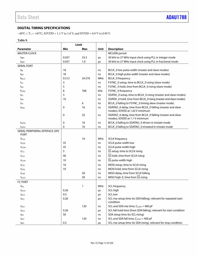
Rev. 0 | Page 13 of 226
DIGITAL TIMING SPECIFICATIONS −40°C < TA < +85°C, IOVDD = 1.1 V to 1.8 V, and DVDD = 0.9 V to 0.99 V.
Table 9. Limit Parameter Min Max Unit Description MASTER CLOCK MCLKIN period
tMPI 0.037 33.3 µs 30 kHz to 27 MHz input clock using PLL in integer mode tMPF 0.037 1.0 µs 30 kHz to 27 MHz input clock using PLL in fractional mode
SERIAL PORT tBL 18 ns BCLK_0 low pulse width (master and slave modes) tBH 18 ns BCLK_0 high pulse width (master and slave modes) fBCLK 0.512 24.576 MHz BCLK_0 frequency tLS 3 ns FSYNC_0 setup, time to BCLK_0 rising (slave mode) tLH 5 ns FSYNC_0 hold, time from BCLK_0 rising (slave mode) fSYNC 8 768 kHz FSYNC_0 frequency tSS 3 ns SDATAI_0 setup, time to BCLK_0 rising (master and slave modes) tSH 10 ns SDATAI_0 hold, time from BCLK_0 rising (master and slave modes) tTS 6 ns BCLK_0 falling to FSYNC_0 timing skew (master mode) tSOD 0 16 ns SDATAO_0 delay, time from BCLK_0 falling (master and slave
modes), IOVDD at 1.62 V minimum 0 32 ns SDATAO_0 delay, time from BCLK_0 falling (master and slave
modes), IOVDD at 1.1 V minimum tSOTD 0 16 ns BCLK_0 falling to SDATAO_0 driven in tristate mode tSOTX 0 16 ns BCLK_0 falling to SDATAO_0 tristated in tristate mode
SERIAL PERIPHERAL INTEFACE (SPI) PORT
fSCLK 10 MHz SCLK frequency tCCPL 35 ns SCLK pulse width low tCCPH 35 ns SCLK pulse width high tCLS 5 ns SS setup, time to SCLK rising
tCLH 40 ns SS hold, time from SCLK rising
tCLPH 10 ns SS pulse width high
tCDS 10 ns MOSI setup, time to SCLK rising tCDH 10 ns MOSI hold, time from SCLK rising tCOD 30 ns MISO delay, time from SCLK falling tCOTS 30 ns MISO high-Z, time from SS rising
I2C PORT fSCL 1 MHz SCL frequency tSCLH 0.26 µs SCL high tSCLL 0.5 µs SCL low tSCS 0.26 µs SCL rise setup time (to SDA falling), relevant for repeated start
condition tSCR 120 ns SCL and SDA rise time, CLOAD = 400 pF tSCH 0.26 µs SCL fall hold time (from SDA falling), relevant for start condition tDS 50 ns SDA setup time (to SCL rising) tSCF 120 ns SCL and SDA fall time, CLOAD = 400 pF tBFT 0.5 µs SCL rise setup time (to SDA rising), relevant for stop condition

ADAU1788 Data Sheet
Rev. 0 | Page 14 of 226
Limit Parameter Min Max Unit Description GENERAL-PURPOSE INPUT/
OUTPUT (GPIO) PINS
tGIL 1.5 × 1/fS µs MPx input latency, time until high or low value is read by core tRLPW 20 ns PD low pulse width
DIGITAL MICROPHONE tCF
1 12 ns Digital microphone clock fall time tCR
1 14 ns Digital microphone clock rise time tSETUP 10 ns Digital microphone data setup time tHOLD 3 ns Digital microphone data hold time
PDM OUTPUT fPDM_CLK PDM clock frequency 3.072 MHz 3 MHz setting 6.144 MHz 6 MHz setting tCF
1 12 ns Digital PDM clock output fall time tCR
1 14 ns Digital PDM clock output rise time tHOLD 35 46 ns PDM data hold time
1 Digital microphone clock rise and fall times are measured at 2 mA drive strength with 25 pF load.
Digital Timing Diagrams
BCLK_0
FSYNC_0
SDATAx_0LEFT JUSTIFIED
MODE
LSB
SDATAx_0I2S MODE
SDATAx_0RIGHT JUSTIFIED
MODE
tBH
MSB MSB – 1
MSB
MSB
8 BIT CLOCKS(24-BIT DATA)
12 BIT CLOCKS(20-BIT DATA)
14 BIT CLOCKS(18-BIT DATA)
16 BIT CLOCKS(16-BIT DATA)
tLS
tSS
tSH
tSH
tSS
tSS
tSH
tSS
tSH
tLHtBL
2053
4-00
2
Figure 2. Serial Input Port Timing Diagram
Data Sheet ADAU1788
Rev. 0 | Page 15 of 226
FSYNC_0
LSB
SDATAx_0I2S MODE
SDATAx_0RIGHT JUSTIFIED
MODE
MSB
SDATAx_0LEFT JUSTIFIED
MODEMSB MSB – 1
SDATAx_0WITH TRISTATE MSB LSB
MSB
8 BIT CLOCKS(24-BIT DATA)
12 BIT CLOCKS(20-BIT DATA)
14 BIT CLOCKS(18-BIT DATA)
16 BIT CLOCKS(16-BIT DATA)
tLS
tSOD
tSOD
tSOTD
tSOD
tSOTX
tLHtTS
tBL
BCLK_0
tBH
HIGH-Z HIGH-Z
2053
4-00
3
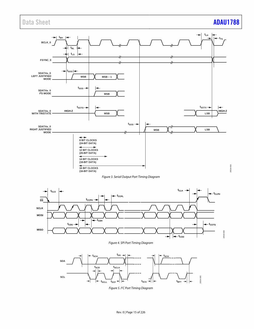
Figure 3. Serial Output Port Timing Diagram
tCDS
tCDH
SS
SCLK
MOSI
MISO
tCLS
tCCPH
tCCPL
tCLHtCLPH
tCOTS
tCOD 2053
4-00
4
Figure 4. SPI Port Timing Diagram
tSCH
tSCLHtSCR
tSCLL tSCF
tDS
SDA
SCL
tSCH
tBFTtSCS 2053
4-00
5
Figure 5. I2C Port Timing Diagram
ADAU1788 Data Sheet
Rev. 0 | Page 16 of 226
R L R L
tHOLD
tSETUP
tCR tCF
2053
4-00
7
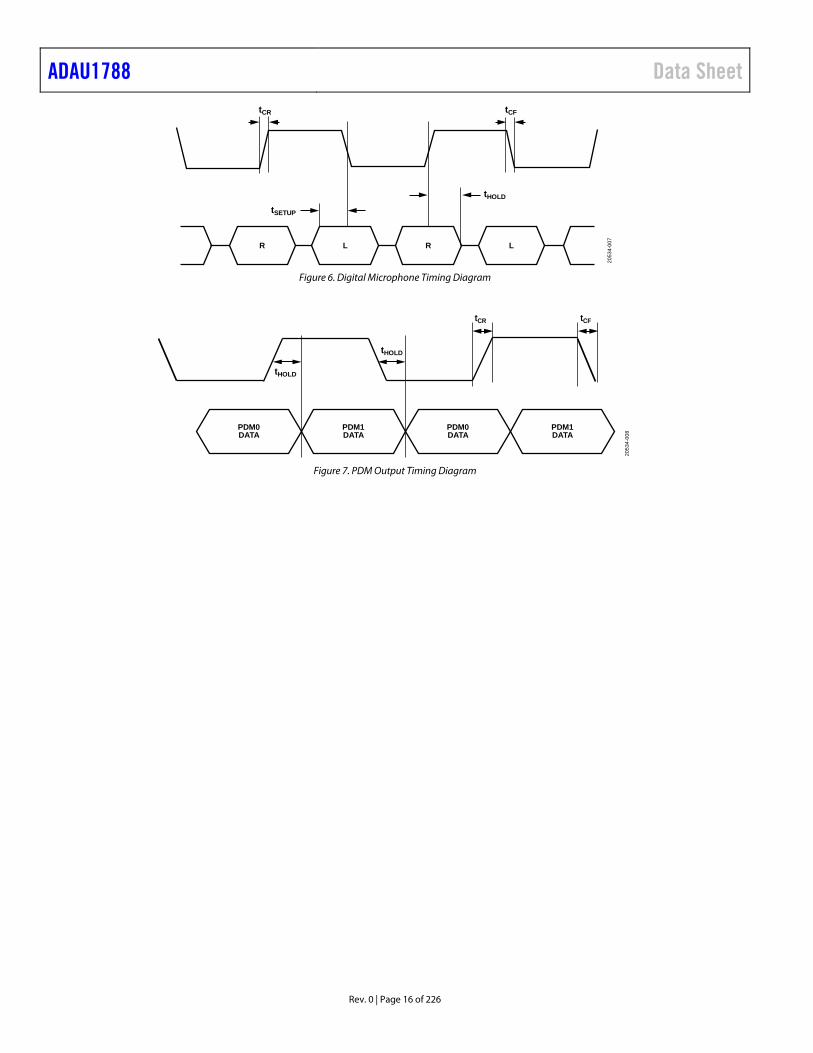
Figure 6. Digital Microphone Timing Diagram
PDM0DATA
PDM1DATA
tHOLD
tHOLD
PDM0DATA
PDM1DATA
tCR tCF
2053
4-00
8
Figure 7. PDM Output Timing Diagram

Data Sheet ADAU1788
Rev. 0 | Page 17 of 226
ABSOLUTE MAXIMUM RATINGS Table 10. Parameter Rating Power Supply (AVDD, IOVDD) −0.3 V to +1.98 V Digital Supply (DVDD) −0.3 V to +1.21 V Input Current (Except Supply Pins) ±20 mA Analog Input Voltage (Signal Pins) –0.3 V to AVDD + 0.3 V Digital Input Voltage (Signal Pins) −0.3 to IOVDD + 0.3 V Operating Temperature Range (Case) −40°C to +85°C Storage Temperature Range −65°C to +150°C
Stresses at or above those listed under Absolute Maximum Ratings may cause permanent damage to the product. This is a stress rating only; functional operation of the product at these or any other conditions above those indicated in the operational section of this specification is not implied. Operation beyond the maximum operating conditions for extended periods may affect product reliability.
THERMAL RESISTANCE Thermal performance is directly linked to printed circuit board (PCB) design and operating environment. Careful attention to PCB thermal design is required.
θJA and θJC are determined according to JESD51-9 on a 4-layer PCB with natural convection cooling.
Table 11. Thermal Resistance Package Type θJA
1 θJC1 Unit
CB-42-2 46.7 0.3 °C/W
1 Thermal impedance simulated values are based on a JEDEC 2S2P thermal test board with two thermal vias. See JEDEC JESD-51.
ESD CAUTION

ADAU1788 Data Sheet
Rev. 0 | Page 18 of 226
PIN CONFIGURATION AND FUNCTION DESCRIPTIONS
BALL A1INDICATOR
ADAU1788TOP VIEW
(BALL SIDE DOWN)
SCL/SCLK
XTALO
DMIC_CLK0/MP7
ADDR1/MOSI
MICBIAS1
MICBIAS0
SDA/MISO
DMIC01/MP9
XTALI/MCLKINDGND
MP3
IOVDDDVDD
DMIC23/MP10
ADDR0/SS
1 2 3 4
A
B
C
D
E AVDDAIN1REG_EN
PD
NC
RESERVED
AGNDRESERVEDAGND CM AIN0
DMIC_CLK1/MP8 MP5 MP6 MP4
NC RESERVED
BCLK_0/MP1
FSYNC_0/MP0
HPOUTP0/LOUTP0
AVDD
NC
HPVDD
SDATAO_0
SDATAI_0/MP2
HPGND
HPOUTN0/LOUTN0
5 6
F
7
2053
4-00
9
NC = NO CONNECTION. LEAVE THIS PIN OPEN. Figure 8. Ball Configuration (Top View)
Table 12. Ball Function Descriptions Ball No. Mnemonic Type1 Description A1 SDATAO_0 D_IO Serial Audio Port 0 Output Data. A2 BCLK_0/MP1 D_IO Serial Audio Port 0 Bit Clock (BCLK_0). Multipurpose Input/Output 1 (MP1). A3 DVDD PWR Digital Core Supply. The digital supply can be generated from an on-board regulator or
supplied directly from an external supply. In each case, decouple DVDD to DGND with a 1 µF and a 0.1 μF capacitor.
A4 DGND PWR Digital Ground. The AGND and DGND pins can be tied directly together in a common ground plane.
A5 IOVDD PWR Supply for the Digital Input and Output Pins. The digital output pins are supplied from IOVDD, and this pin sets the highest input voltage seen on the digital input pins. The current draw of this pin is variable because the current is dependent on the loads of the digital outputs. Decouple IOVDD to DGND with a 0.1 μF capacitor.
A6 XTALO A_OUT Crystal Clock Output. This pin is the output of the crystal amplifier. Do not use this pin to provide a clock to other ICs in the system.
A7 XTALI/MCLKIN D_IN Crystal Clock Input (XTALI). Master Clock Input (MCLKIN).

Data Sheet ADAU1788
Rev. 0 | Page 19 of 226
Ball No. Mnemonic Type1 Description B1 SDATAI_0/MP2 D_IO Serial Audio Port 0 Input Data (SDATAI_0). Multipurpose Input/Output 2 (MP2). B2 FSYNC_0/MP0 D_IO Serial Audio Port 0 Frame Sync/Left Right Clock (FSYNC_0). Multipurpose Input/Output 0 (MP0). B3 DMIC23/MP10 D_IO Digital Microphone Stereo Input 2 and Digital Microphone Stereo Input 3 (DMIC23). Multipurpose Input/Output 10 (MP10). B4 DMIC_CLK0/MP7 D_IO Digital Microphone Clock Output 0 (DMIC_CLK0). Multipurpose Input/Output 7 (MP7). B5 DMIC01/MP9 D_IO Digital Microphone Stereo Input 0 and Digital Microphone Stereo Input 1 (DMIC01). Multipurpose Input/Output 9 (MP9). B6 SDA/MISO D_IO I2C Data (SDA). This pin is a bidirectional open-collector input. The line connected to this pin
must have a 2.0 kΩ pull-up resistor. SPI Data Output (MISO). This SPI data output is used for reading back registers and memory
locations. This pin is tristated when an SPI read is not active. B7 SCL/SCLK D_IN I2C Clock (SCL). This pin is always an open-collector input when the device is in I2C control
mode. When the device is in self-boot mode, this pin is an open-collector output (I2C master). The line connected to this pin must have a 2.0 kΩ pull-up resistor.
SPI Clock (SCLK). This pin can either run continuously or be gated off between SPI transactions. C1 NC NC No Connection. Leave this pin open. C2 DMIC_CLK1/MP8 D_IO Digital Microphone Clock Output 1 (DMIC_CLK1). Multipurpose Input/Output 8 (MP8). C3 MP5 D_IO Multipurpose Input/Output 5 (MP5). Connect this pin to DGND if not used. C4 MP6 D_IO Multipurpose Input/Output 6 (MP6). Connect this pin to DGND if not used. C5 MP4 D_IO Multipurpose Input/Output 4 (MP4). Connect this pin to DGND if not used. C6 ADDR0/SS D_IN I2C Address 0 (ADDR0).
SPI Latch Signal (SS). This pin must go low at the beginning of an SPI transaction and high at the end of a transaction. Each SPI transaction may take a different number of SCLK cycles to complete, depending on the address and read/write bit that are sent at the beginning of the SPI transaction.
C7 ADDR1/MOSI D_IN I2C Address 1 (ADDR1). SPI Data Input (MOSI). D1 HPVDD PWR Headphone Amplifier Power, 1.8 V Analog Supply. Decouple this pin to HPGND with a 0.1 μF
capacitor. The PCB trace to this pin must be wider to supply the higher current necessary for driving the headphone outputs.
D2 NC NC No Connection. Leave this pin open. D3 RESERVED D_IN Internal Use Only. Connect this pin to DGND. D4 PD D_IN Active Low Power-Down. All digital and analog circuits are powered down. There is an internal
pull-down resistor on this pin. Therefore, the ADAU1788 is held in power-down mode if the input signal is floating while power is applied to the supply pins.
D5 MP3 D_IO Multipurpose Input/Output 3. Connect this pin to DGND if not used. D6 RESERVED D_IN Internal use only. Connect this pin to DGND. D7 MICBIAS0 A_OUT Bias Voltage for Electret Microphone 0. Decouple this pin with a 1 µF capacitor. E1 HPGND PWR Headphone Amplifier Ground. E2 HPOUTP0/LOUTP0 A_OUT Headphone Output Noninverted Channel 0 (HPOUTP0). Line Output Noninverted Channel 0 (LOUTP0). E3 REG_EN A_IN Regulator Enable. Tie this pin to AVDD to enable the regulator and tie this pin to ground to
disable the regulator. E4 NC No Connection. Leave this pin open. E5 AIN1 A_IN ADC1 Input. E6 MICBIAS1 A_OUT Bias Voltage for Electret Microphone 1. Decouple this pin with a 1 µF capacitor. E7 AVDD PWR 1.8 V Analog Supply. Decouple this pin to AGND with a 0.1 μF capacitor.

ADAU1788 Data Sheet
Rev. 0 | Page 20 of 226
Ball No. Mnemonic Type1 Description F1 HPOUTN0/LOUTN0 A_OUT Headphone Output Noninverted Channel 0 (HPOUTP0). Line Output Noninverted Channel 0 (LOUTP0). F2 AVDD PWR 1.8 V Analog Supply. Decouple AVDD to AGND with a 0.1 μF capacitor. F3 AGND PWR Analog Ground. The AGND and DGND pins can be tied directly together in a common ground
plane. F4 CM A_OUT Common-Mode Reference, Fixed at 0.85 V Nominal. Connect a 10 μF and a 0.1 μF decoupling
capacitor between this pin and AGND to reduce crosstalk between the ADCs and the DAC. The material of the capacitors is not critical. This pin can bias external analog circuits as long as the circuits are not drawing current from CM (for example, the noninverting input of an op amp).
F5 RESERVED A_IN Internal Use Only. Connect this pin to CM. F6 AIN0 A_IN ADC0 Input. F7 AGND PWR Analog Ground. 1 D_IO means digital input/output, PWR means power, A_OUT means analog output, D_IN means digital input, NC means no connection, and A_IN means analog input.
Data Sheet ADAU1788
Rev. 0 | Page 21 of 226
TYPICAL PERFORMANCE CHARACTERISTICS
FREQUENCY (Hz)100 1k 10k
RELA
TIVE
LEV
EL (d
B)
–3.0–2.8–2.6–2.4–2.2–2.0–1.8–1.6–1.4–1.2–1.0–0.8–0.6–0.4–0.2
00.20.4
ADCx_HPF_EN = ON, ADCxx_FCOMP = ONADCx_HPF_EN = OFF, ADCxx_FCOMP = OFF
2053
4-01
0
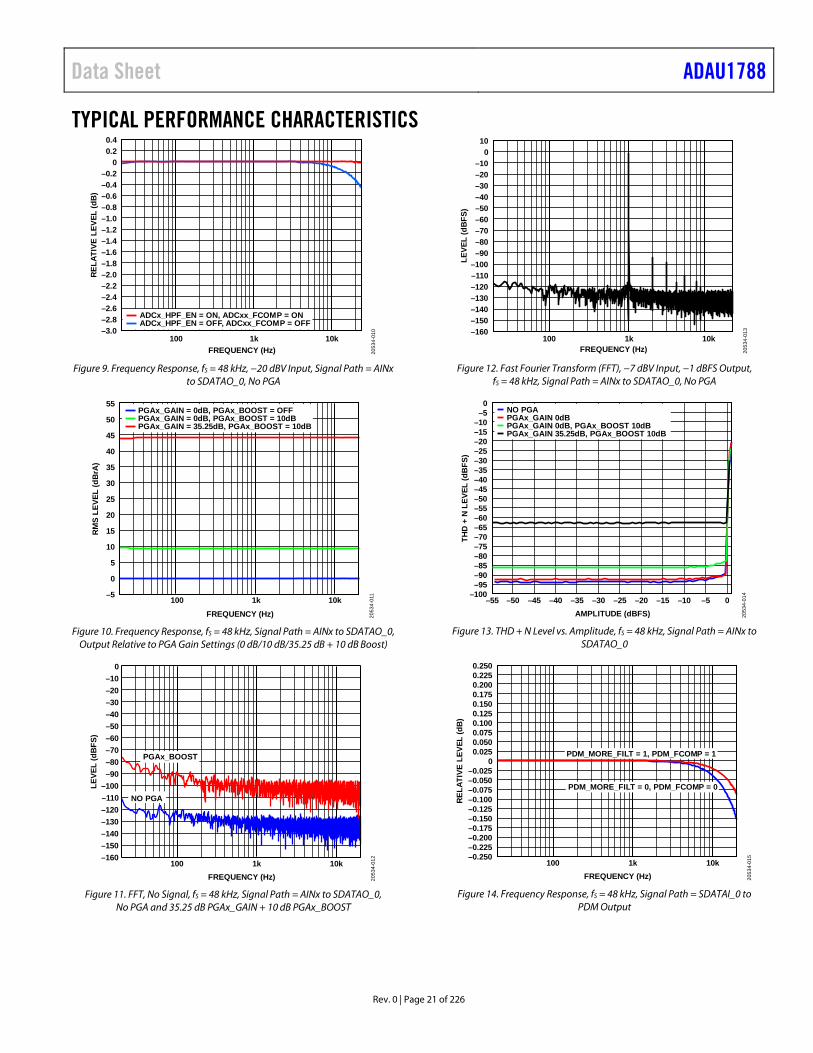
Figure 9. Frequency Response, fS = 48 kHz, −20 dBV Input, Signal Path = AINx
to SDATAO_0, No PGA
RMS
LEVE
L (d
BrA)
–5
0
5
10
15
20
25
30
35
40
45
50
55
FREQUENCY (Hz)100 1k 10k
PGAx_GAIN = 0dB, PGAx_BOOST = OFFPGAx_GAIN = 0dB, PGAx_BOOST = 10dBPGAx_GAIN = 35.25dB, PGAx_BOOST = 10dB
2053
4-01
1
Figure 10. Frequency Response, fS = 48 kHz, Signal Path = AINx to SDATAO_0,
Output Relative to PGA Gain Settings (0 dB/10 dB/35.25 dB + 10 dB Boost)
FREQUENCY (Hz)100 1k 10k
LEVE
L (d
BFS)
–160–150–140–130–120–110–100–90–80–70–60–50–40–30–20–10
0
PGAx_BOOST
NO PGA
2053
4-01
2
Figure 11. FFT, No Signal, fS = 48 kHz, Signal Path = AINx to SDATAO_0,
No PGA and 35.25 dB PGAx_GAIN + 10 dB PGAx_BOOST
FREQUENCY (Hz)100 1k 10k
LEVE
L (d
BFS)
–160–150–140–130–120–110–100
–90–80–70–60–50–40–30–20–10
010
2053
4-01
3
Figure 12. Fast Fourier Transform (FFT), −7 dBV Input, −1 dBFS Output,
fS = 48 kHz, Signal Path = AINx to SDATAO_0, No PGA
AMPLITUDE (dBFS)–50–55 –45 –40 –35 –30 –25 –20 –15 –10 –5 0
THD
+ N
LEVE
L (d
BFS)
–95–100
–90–85–80–75–70–65–60–55–50–45–40–35–30–25–20–15–10
–50
NO PGAPGAx_GAIN 0dBPGAx_GAIN 0dB, PGAx_BOOST 10dBPGAx_GAIN 35.25dB, PGAx_BOOST 10dB
2053
4-01
4
Figure 13. THD + N Level vs. Amplitude, fS = 48 kHz, Signal Path = AINx to
SDATAO_0
FREQUENCY (Hz)100 1k 10k
RELA
TIVE
LEV
EL (d
B)
–0.250–0.225–0.200–0.175–0.150–0.125–0.100–0.075–0.050–0.025
00.0250.0500.0750.1000.1250.1500.1750.2000.2250.250
PDM_MORE_FILT = 1, PDM_FCOMP = 1
PDM_MORE_FILT = 0, PDM_FCOMP = 0
2053
4-01
5
Figure 14. Frequency Response, fS = 48 kHz, Signal Path = SDATAI_0 to
PDM Output

ADAU1788 Data Sheet
Rev. 0 | Page 22 of 226
FREQUENCY (Hz)
LEVE
L (d
BFS)
–190–180–170–160–150–140–130–120–110–100
–90–80–70–60–50–40–30–20–10
0 PDM CLOCK = 3.072MHzPDM CLOCK = 6.144MHz
100 1k 10k
2053
4-01
6
Figure 15. FFT, No Signal, fS = 48 kHz Throughout, Signal Path = SDATAI_0 to
FastDSP to PDM Output
FREQUENCY (Hz)100 1k 10k
LEVE
L (d
BFS)
–190–180–170–160–150–140–130–120–110–100
–90–80–70–60–50–40–30–20–10
0 PDM CLOCK = 3.072MHzPDM CLOCK = 6.144MHz
2053
4-01
7
Figure 16. FFT, −7 dBFS, fS = 48 kHz Throughout, Signal Path = SDATAI_0 to
FastDSP to PDM Output
FREQUENCY (Hz)100 1k 10k
PSRR
+ N
(dBr
A)
–70–65–60–55–50–45–40–35–30–25–20–15–10–50
ADC0ADC1
2053
4-01
8
Figure 17. PSRR + N, Signal Path = AINx to SDATAO_0, fS = 48 kHz, 100 mV p-p Ripple Input on AVDD, No PGA (0 dBrA = −23.3 dBFS)
FREQUENCY (Hz)100 1k 10k
PSRR
+ N
(dBr
A)
–70–65–60–55–50–45–40–35–30–25–20–15–10
–50
ADC0ADC1
2053
4-01
9
Figure 18. PSRR + N, Signal Path = AINx to SDATAO_0, fS = 48 kHz,
100 mV p-p Ripple Input on AVDD, PGA = 0 dB (0 dBrA = −23.3 dBFS)
100 1k 10kFREQUENCY (Hz)
PSRR
+ N
(dBr
A)
–74–72–70–68–66–64–62–60–58–56–54–52–50–48–46–44–42–40–38–36 ADC0
ADC1
2053
4-02
0
Figure 19. PSRR + N, Signal Path = AINx to SDATAO_0, fS = 48 kHz,
100 mV p-p Ripple Input on AVDD, PGA = 10 dB (0 dBrA = −23.3 dBFS)
100 1k 10kFREQUENCY (Hz)
PSRR
+ N
(dBr
A)
–80–75–70–65–60–55–50–45–40–35–30–25–20–15–10
–50
HPOUTx0
2053
4-02
1
Figure 20. PSRR + N, Signal Path = SDATAI_0 to HPOUTx0, fS = 48 kHz,
100 mV p-p Ripple Input on AVDD (0 dBrA = −29 dBV)

Data Sheet ADAU1788
Rev. 0 | Page 23 of 226
FREQUENCY (Hz)100 1k 10k
LEVE
L (d
BV)
–150–140–130–120–110–100–90–80–70–60–50–40–30–20–10
0 10
2053
4-02
2
Figure 21. FFT, No Signal, fS = 48 kHz, Signal Path = SDATAI_0 to HPOUTx0,
Headphone Mode, Load = 16 Ω
FREQUENCY (Hz)100 1k 10k
LEVE
L (d
BV)
–150–140–130–120–110–100
–90–80–70–60–50–40–30–20–10
0 10
2053
4-02
3
Figure 22. FFT, No Signal, fS = 48 kHz, Signal Path = SDATAI_0 to LOUTx0,
Line Output Mode, Load = 10 kΩ
FREQUENCY (Hz)100 1k 10k
LEVE
L (d
BV)
–150–140–130–120–110–100
–90–80–70–60–50–40–30–20–10
0 10
2053
4-02
4
Figure 23. FFT, −1 dBFS, fS = 48 kHz, Signal Path = SDATAI_0 to HPOUTx0,
Headphone Mode, Load = 32 Ω
FREQUENCY (Hz)100 1k 10k
LEVE
L (d
BV)
–150–140–130–120–110–100
–90–80–70–60–50–40–30–20–10
0 10
2053
4-02
5
Figure 24. FFT, −1 dBFS, fS = 48 kHz, Signal Path = SDATAI_0 to HPOUTx0,
Headphone Mode, Load = 24 Ω
FREQUENCY (Hz)100 1k 10k
LEVE
L (d
BV)
–150–140–130–120–110–100–90–80–70–60–50–40–30–20–10
0 10
2053
4-02
6
Figure 25. FFT, −1 dBFS, fS = 48 kHz, Signal Path = SDATAI_0 to HPOUTx0,
Headphone Mode, Load = 16 Ω
FREQUENCY (Hz)100 1k 10k
LEVE
L (d
BV)
–150–140–130–120–110–100–90–80–70–60–50–40–30–20–10
0 10
2053
4-02
7
Figure 26. FFT, −1 dBFS, fS = 48 kHz, Signal Path = SDATAI_0 to LOUTx0,
Line Output Mode, Load = 10 kΩ
ADAU1788 Data Sheet
Rev. 0 | Page 24 of 226
FREQUENCY (Hz)100 1k 10k
LEVE
L (d
BV)
–150–140–130–120–110–100
–90–80–70–60–50–40–30–20–10
0 10
2053
4-02
8
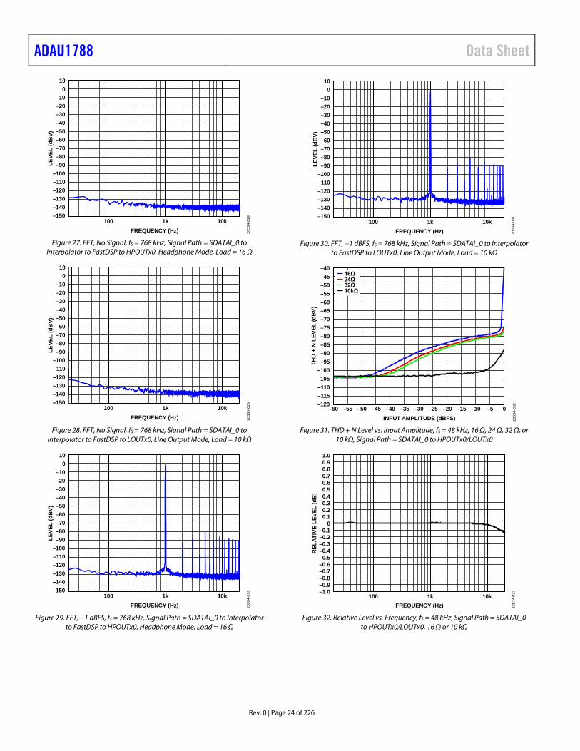
Figure 27. FFT, No Signal, fS = 768 kHz, Signal Path = SDATAI_0 to
Interpolator to FastDSP to HPOUTx0, Headphone Mode, Load = 16 Ω
FREQUENCY (Hz)100 1k 10k
LEVE
L (d
BV)
–150–140–130–120–110–100
–90–80–70–60–50–40–30–20–10
0 10
2053
4-02
9
Figure 28. FFT, No Signal, fS = 768 kHz, Signal Path = SDATAI_0 to
Interpolator to FastDSP to LOUTx0, Line Output Mode, Load = 10 kΩ
FREQUENCY (Hz)100 1k 10k
LEVE
L (d
BV)
–150–140–130–120–110–100
–90–80–70–60–50–40–30–20–10
0 10
2053
4-03
0
Figure 29. FFT, −1 dBFS, fS = 768 kHz, Signal Path = SDATAI_0 to Interpolator
to FastDSP to HPOUTx0, Headphone Mode, Load = 16 Ω
FREQUENCY (Hz)100 1k 10k
LEVE
L (d
BV)
–150–140–130–120–110–100
–90–80–70–60–50–40–30–20–10
0 10
2053
4-03
1
Figure 30. FFT, −1 dBFS, fS = 768 kHz, Signal Path = SDATAI_0 to Interpolator
to FastDSP to LOUTx0, Line Output Mode, Load = 10 kΩ
INPUT AMPLITUDE (dBFS)–55 –50 –45 –40 –35 –30 –25 –20 –15 –10 0–5
THD
+ N
LEVE
L (d
BV)
–60–120–115–110–105–100
–95–90–85–80–75–70–65–60–55–50–45–40
16Ω24Ω32Ω10kΩ
2053
4-03
2
Figure 31. THD + N Level vs. Input Amplitude, fS = 48 kHz, 16 Ω, 24 Ω, 32 Ω, or
10 kΩ, Signal Path = SDATAI_0 to HPOUTx0/LOUTx0
FREQUENCY (Hz)
RELA
TIVE
LEV
EL (d
B)
–1.0–0.9–0.8–0.7–0.6–0.5–0.4–0.3–0.2–0.1
00.10.20.30.40.50.60.70.80.91.0
100 1k 10k
2053
4-03
3
Figure 32. Relative Level vs. Frequency, fS = 48 kHz, Signal Path = SDATAI_0
to HPOUTx0/LOUTx0, 16 Ω or 10 kΩ

Data Sheet ADAU1788
Rev. 0 | Page 25 of 226
FREQUENCY (Hz)
RELA
TIVE
LEV
EL (d
B)
–1.0–0.9–0.8–0.7–0.6–0.5–0.4–0.3–0.2–0.1
00.10.20.30.40.50.60.70.80.91.0
100 1k 10k
32Ω24Ω16Ω10kΩ
2053
4-03
4
Figure 33. Relative Level vs. Frequency, fS = 768 kHz, Signal Path = SDATAI_0
to Interpolator to FastDSP to HPOUTx0/LOUTx0, 16 Ω to 10 kΩ
FREQUENCY (Hz)
RELA
TIVE
LEV
EL (d
B)
–1.0–0.9–0.8–0.7–0.6–0.5–0.4–0.3–0.2–0.1
00.10.20.30.40.50.60.70.80.91.0
100 1k 10k
ASRC DISABLEDASRC ENABLED
2053
4-03
5
Figure 34. Relative Level vs. Frequency, fS = 48 kHz Throughout Except FastDSP = 768 kHz, Signal Path = SDATAI_0 to ASRCI to SigmaDSP to
Interpolator to FastDSP to Decimator to ASRCO to SDATAO_0
FREQUENCY (Hz)100 1k 10k
LEVE
L (d
BFS)
–190–180–170–160–150–140–130–120–110–100–90–80–70–60–50–40–30–20–10
0
2053
4-03
6
Figure 35. FFT, No Signal, fS = 48 kHz Throughout Except FastDSP = 768 kHz, Signal Path = SDATAI_0 to ASRCI to SigmaDSP to Interpolator to FastDSP to
Decimator to ASRCO to SDATAO_0
FREQUENCY (Hz)100 1k 10k
LEVE
L (d
BFS)
–190–180–170–160–150–140–130–120–110–100
–90–80–70–60–50–40–30–20–10
0
2053
4-03
7
Figure 36. FFT, No Signal, fS = 48 kHz Throughout Except FastDSP = 768 kHz,
Signal Path = SDATAI_0 to SigmaDSP to Interpolator to FastDSP to Decimator to SDATAO_0
FREQUENCY (Hz)100 1k 10k
LEVE
L (d
BFS)
–190–180–170–160–150–140–130–120–110–100–90–80–70–60–50–40–30–20–10
0
2053
4-03
8
Figure 37. FFT, −1 dBFS, fS = 48 kHz Throughout Except FastDSP = 768 kHz,
Signal Path = SDATAI_0 to ASRCI to SigmaDSP to Interpolator to FastDSP to Decimator to ASRCO to SDATAO_0
FREQUENCY (Hz)100 1k 10k
LEVE
L (d
BFS)
–190–180–170–160–150–140–130–120–110–100
–90–80–70–60–50–40–30–20–10
0
2053
4-03
9
Figure 38. FFT, −1 dBFS, fS = 48 kHz Throughout Except FastDSP = 768 kHz,
Signal Path = SDATAI_0 to SigmaDSP to Interpolator to FastDSP to Decimator to SDATAO_0

ADAU1788 Data Sheet
Rev. 0 | Page 26 of 226
FREQUENCY (Hz)
GRO
UP D
ELAY
(SM
OO
TH) (
µs)
0102030405060708090
100110120130140150160170180190
100 1k 10k
48kHz96kHz192kHz384kHz768kHz
2053
4-04
0
Figure 39. Group Delay (Smooth) vs. Frequency, fS = 192 kHz to 768 kHz,
Signal Path = AINx to FastDSP to HPOUTx0/LOUTx0
FREQUENCY (Hz)100 1k 10k
LEVE
L (d
BFS)
–190–180–170–160–150–140–130–120–110–100
–90–80–70–60–50–40–30–20–10
0 DMIC_CLKx RATE = 3.072MHzDMIC_CLKx RATE = 6.144MHz
2053
4-04
1
Figure 40. FFT, No Signal, DMIC_CLKx_RATE = 3.072 MHz to 6.144 MHz,
Signal Path = DMICxx to SDATAO_0
FREQUENCY (Hz)100 1k 10k
RELA
TIVE
LEV
EL (d
B)
–0.50–0.45–0.40–0.35–0.30–0.25–0.20–0.15–0.10–0.05
00.050.100.150.200.250.300.350.400.450.50
2053
4-04
2
Figure 41. Relative Level vs. Frequency, DMIC_CLKx_RATE = 3.072 MHz to
6.144 MHz, Signal Path = DMICxx to SDATAO_0
LEVE
L (d
BFS)
–190100 1k 10k
–180–170–160–150–140–130–120–110–100–90–80–70–60–50–40–30–20–10
0
FREQUENCY (Hz) 2053
4-04
3
Figure 42. FFT, −10 dBFS, DMIC_CLKx_RATE = 3.072 MHz, Signal Path =
DMICxx to SDATAO_0
LEVE
L (d
BFS)
–190–180–170–160–150–140–130–120–110–100–90–80–70–60–50–40–30–20–10
0
FREQUENCY (Hz)1k 10k100
2053
4-04
4
Figure 43. FFT, −10 dBFS, DMIC_CLKx_RATE = 3.072 MHz, Signal Path =
DMICxx to SDATAO_0
AMPLITUDE (dBFS)–65 –60 –55 –50 –45 –40 –35 –30 –25 –20 –15 –10
THD
+ N
LEVE
L (d
BFS)
–140
–135
–130
–125
–120
–115
–110
–105
–100
–95
–90
–85
–80DMIC_CLKx RATE = 3.072MHz (FIFTH-ORDER)DMIC_CLKx RATE = 6.144MHz (FIFTH-ORDER)
2053
4-04
5
Figure 44. THD + N Level vs. Amplitude, −10 dBFS, DMIC_CLKx_RATE =
3.072 MHz to 6.144 MHz, Signal Path = DMICxx to SDATAO_0

Data Sheet ADAU1788
Rev. 0 | Page 27 of 226
FREQUENCY (Hz)
RELA
TIVE
LEV
EL (d
B)
100 1k 10k
48kHz768kHz
–0.50–0.45–0.40–0.35–0.30–0.25–0.20–0.15–0.10–0.05
00.050.100.150.200.250.300.350.400.450.50
2053
4-04
7
Figure 45. Relative Level vs. Frequency, Headphone/Line Output Mode,
Load = 16 Ω to 10 kΩ, fS = 48 kHz and 768 kHz, Signal Path = AIN0 to DAC0
AMPLITUDE (dBV)–55–60 –50 –45 –40 –35 –30 –25 –20 –15 –10 0
THD
+ N
LEVE
L (d
BV)
–90
–100
–80
–70
–60
–50
–40
–30
–20
–10
0
10
2010kΩ16Ω
2053
4-04
8
Figure 46. THD + N Level vs. Amplitude, fS = 48 kHz to 768 kHz, Load = 10 kΩ
and 16 Ω, Signal Path = AINx to HPOUTx0/LOUTx0
FREQUENCY (Hz)
LEVE
L (d
BV)
–160–150–140–130–120–110–100
–90–80–70–60–50–40–30–20–10
010203040
100 1k 10k
2053
4-04
9
Figure 47. FFT, −1 dBV, Line Output Mode, Load = 10 kΩ, fS = 48 kHz to
768 kHz, Signal Path = AIN0 to LOUTx0
FREQUENCY (Hz)
LEVE
L (d
BV)
–160–150–140–130–120–110–100
–90–80–70–60–50–40–30–20–10
010203040
100 1k 10k
2053
4-05
0
Figure 48. FFT, −1 dBV, Headphone Mode, Load = 16 Ω, fS = 48 kHz to
768 kHz, Signal Path = AINx to HPOUTx0
100 1k 10kFREQUENCY (Hz)
LEVE
L (d
BV)
–160–150–140–130–120–110–100
–90–80–70–60–50–40–30–20–10
010203040
2053
4-05
1
Figure 49. FFT, No Signal, Load = 16 Ω to 10 kΩ, fS = 48 kHz to 768 kHz,
Signal Path = AINx to HPOUTx0/LOUTx0

ADAU1788 Data Sheet
Rev. 0 | Page 28 of 226
SYSTEM BLOCK DIAGRAM
1µF 0.1µF
18pF18pF
SigmaDSP50 MIPs
ADC DECIMATION8kHz TO768kHz
OUTPUT
DIGITALMIC
DECIMATION8kHz TO768kHz
OUTPUT
ADC
4DMIC
2ADC
MICROPHONEBIAS
GENERATOR
MICBIAS0
SERIAL AUDIO PORT 0MASTER OR SLAVE
16
16
ROUTE
I2C OR SPICONTROL PORT
ADDR
0/SS
ADDR
1/M
OSI
SCL/
SCLK
SDA/
MIS
O
SAI_0
16 FastDSP64
INSTRUCTIONS
SAI_0
SDSP
16
FDSP
ROUTESAI_0
ASRCI
LDO
HPG
ND
AGND
AGND
DGND
CLKOSCILLATOR PLL
BCLK_0FSYNC_0
MCLK
ROUTE
SAI_0
ADC
ASRCI
FDSP
SDSP
DAC HP
ROUTE44 4 4
ASRCO
CMGENERATOR
MICBIAS1
AIN0
AIN1
DMIC_CLK0DMIC_CLK1
DMIC01DMIC23
SAI_
0
ADC
DMIC
ASRCI
FDSP
ADC
DMIC
ASRCI
SDSP
SAD
ATAO
_0IO
VDD
HPVD
D
AVDD
AVDD
DVDD
XTAL
O
CM RESE
RVED
(F5)
REG
_EN
XTAL
I/M
CLKI
N
HPOUTP0
ADAU1788
HPOUTN0MICROPHONE
INPUT 1
MICROPHONEINPUT 2
CONNECT TO GND FOR I2C/SPI CONTROL
SERIAL PORT OFBLUETOOTH
IN THE SYSTEM
THE SERIAL PORT CAN BE CONFIGUREDAS MASTER OR SLAVE
PD PULL TO IOVDDFOR OPERATIONPULL TO GNDFOR POWERDOWN
TO MICROCONTROLLERIN THE SYSTEM
TO GND
SPEAKERLEFT16Ω TO 32Ω
1.8V
1.2V TO1.8V
IF USING EXTERNAL OSCILLATOR ORCLOCK (30kHz TO 27MHz) IN THE SYSTEMCONNECT DIRECTLY TO MCLKIN PININSTEAD OF CRYSTAL OSCILLATOR
0.1µF 0.1µF 0.1µF
0.1µF
10µF
1µF 0.1µF
CONNECT TO AVDD FORINTERNAL REGULATORCONNECT TO GND FOR
EXTERNAL DVDD
0.9V
1kΩ
12.288MHz OR 24.576MHz TYPICALPLEASE CHECK WITH C RYSTALMANUFACTURER FOR REQUIREDLOAD CAPACITOR AND RESISTOR VALUES
IOVDD (1.2V TO 1.8V)10kΩ
10kΩ
SEE
NOTE
TO I2C CONTROLLER IN THE SYSTEMNOTE: I2C DEVICE ADDRESS PINS
SCL
SDA
ADDR0ADDR1
IOVDDGND
IOVDDGNDIOVDD
IOVDD
GNDGND
I2C DEVICE ADDRESS0x280x290x2A0x2B
MP4
(D6)
RES
ERVE
D
BCLK
_0/M
P1
MP3
MP5
MP6
FSYN
C_0/
MP0
SDAT
AI_0
/MP2
(D3)
RES
ERVE
D
2053
4-05
7
DIGITALMICROPHONE1
DIGITALMICROPHONE2
DIGITALMICROPHONE3
DIGITALMICROPHONE4
INPUTASYNCHRONOUS
SAMPLE RATECONVERTER
OUTPUTASYNCHRONOUS
SAMPLE RATECONVERTER
Figure 50. ADAU1788 System Block Diagram with Analog Microphones, Self Boot Mode

Data Sheet ADAU1788
Rev. 0 | Page 29 of 226
THEORY OF OPERATION The ADAU1788 is a low power audio codec with optimized audio processing cores, making the device ideal for noise cancelling applications that require high quality audio, low power, small size, and low latency. The two ADC and one DAC channels each have an SNR of at least 96 dB and a THD + N level of at least −88 dB. The serial audio port is compatible with I2S, left justified, right justified, and TDM modes, with tristating for interfacing to digital audio data. The operating voltage is 1.8 V, with an on-board regulator generating the digital supply voltage. If desired, the regulator can be powered down, and the voltage can be supplied externally.
The input signal path includes flexible configurations that can accept single-ended analog microphone inputs as well as up to eight digital microphone inputs. Two microphone bias pins provide seamless interfacing to electret microphones. Each input signal has its own PGA for volume adjustment.
The ADCs and DAC are high quality, 24-bit Σ-Δ converters that operate at a selectable 12 kHz to 768 kHz sampling rate. The ADCs and DAC have an optional high-pass filter with a cutoff frequency of 1 Hz and fine-step digital soft volume controls.
The mono DAC output is capable of differentially driving a headphone earpiece speaker with 16 Ω impedance or higher. There is also the option to change to line output mode when the output is lightly loaded.
The SigmaDSP core is optimized for low power audio processing. This core can be graphically programmed using the SigmaStudio® software from Analog Devices, Inc. This software includes a library of audio processing blocks such as filters, dynamics
processors, mixers, and low level DSP functions for fast, graphical development of custom signal flows.
The FastDSP core has a reduced instruction set that optimizes this codec for noise cancellation. The program random access memory (RAM) and parameter RAM can be loaded with a custom audio processing signal flow built using SigmaStudio. The values stored in the parameter RAM control individual signal processing blocks.
Use the SigmaStudio software to program and control the cores through the control port. Along with designing and tuning a signal flow, the tools can configure all of the ADAU1788 registers. The SigmaStudio graphical user interface (GUI) allows anyone with digital or analog audio processing knowledge to design the DSP signal flow and export the flow to a target application. The interface also provides enough flexibility and programmability for an experienced DSP programmer to have control of the design. In SigmaStudio, the user can connect graphical blocks (such as biquad filters, volume controls, and arithmetic operations), compile the design, and load the program and parameter files into the ADAU1788 memory through the control port.
The ADAU1788 can generate the internal clocks from a wide range of input clocks by using the on-board bypassable fractional PLL. The PLL accepts inputs from 30 kHz to 27 MHz. For standalone operation, the clock can be generated using the on-board crystal oscillator.
The ADAU1788 is provided in a small, 42-ball, 2.695 mm × 2.320 mm WLCSP.
ADAU1788 Data Sheet
Rev. 0 | Page 30 of 226
SYSTEM CLOCKING AND POWER-UP POWER-DOWN OPERATION AND OPTIONS When pulled low, the PD pin puts the chip in the lowest power state, hardware full chip power-down. If the regulator is used, it also powers down during this state. The chip fully resets in this state and retains no state memory. No communication with the device is possible when the PD pin is low.
By default, out of reset, the chip is in the lowest power state that can be entered via a control interface, software full chip power-down. To enter or exit this power state, use the POWER_EN bit, Bit 0 of Register 0xC00D. When POWER_EN = 0, the I2C/SPI control ports are operational, and everything else is powered down except for the regulator and the crystal, if used. To achieve the lowest power state, set the XTAL_EN bit (Bit 1 of Register 0xC005) = 0. The digital portion of the chip has several power domains. By default, only the domain that powers the control ports and their associated registers are powered on, and the rest of the digital design has its power supplies gated, and its state is lost.
There are two options to retain additional state memory during a software full chip power-down. The KEEP_SDSP and KEEP_ FDSP bits, Bit 1 and Bit 0 of Register 0xC00C, respectively, can retain the state of the SigmaDSP program and parameter memories and/or the FastDSP program and parameter memories. The control register map always retains its state when POWER_EN = 0.
When POWER_EN = 0, the CM pin or the common-mode output can either maintain its state or not by using the CM_KEEP_ALIVE bit, Bit 4 of Register 0xC00C. When CM_KEEP_ALIVE = 0, the CM voltage is lost when POWER_EN = 0, thus producing the lowest possible software power-down current. However, with CM_KEEP_ALIVE = 0, the ADAU1788 has a longer turn on time because the PLL and other analog blocks rely on the CM voltage. A wait time of 35 ms is needed for CM to charge before any analog blocks, such as the PLL, can be enabled.
Conversely, with CM_KEEP_ALIVE = 1, the power-down current is higher, but the start-up time is faster because the 35 ms wait time can be omitted.
If CM_KEEP_ALIVE = 1, use the CM_STARTUP_OVER bit, Bit 2 of Register 0xC00D, to fast charge the CM voltage and to have the lowest turn on time by setting CM_STARUP_OVER = 0 before POWER_EN is set to 1. Then, after the 35 ms wait time, set CM_STARUP_OVER = 1 to keep power consumption low. The reset state of CM_STARTUP_OVER is 0. Therefore, if the PD pin is used to power down the device, the step of setting CM_STARTUP_OVER to 0 can be omitted.
When POWER_EN = 1, the power supplies on the rest of the digital portion of the chip are enabled. Therefore, this register must be set first during the power-up sequence.
The PLL and crystal must be configured and enabled after CM_STARTUP_OVER sequencing is complete. After all the internal digital power supplies are powered up, the PLL is locked, and other needed sequencing is complete, the POWER_UP_ COMPLETE bit (Bit 7, Register 0xC0AB) or an interrupt request (IRQ) indicates such. The IRQ1_POWER_ UP_COMPLETE is Bit 4 of Register 0xC0B1. The IRQ2_ POWER_UP_COMPLETE is Bit 4 of Register 0xC0B4. If the IRQs are used to request an interrupt after POWER_UP_ COMPLETE, the IRQs must be unmasked. The IRQ1_POWER_ UP_COMPLETE_MASK bit (Bit 4, Register 0xC0A4) must be cleared. Similarly, the IRQ2_POWER_UP_COMPLETE (Bit 4, Register 0xC0A7) must be cleared. By default, the IRQs for POWER_UP_COMPLETE are masked.
After POWER_UP_COMPLETE = 1, the DSP memories can be programmed.
The ADAU1788 has highly flexible block level power controls. Each individual channel of each block can be powered on or off separately. There is a control bit, MASTER_BLOCK_EN, that by default is 0 and that overrides all block level enables except for PLL_EN, XTAL_EN, SDSP_EN, and FDSP_EN. The PLL, SigmaDSP, and FastDSP can be enabled, even when MASTER_ BLOCK_EN = 0. All other blocks are always in power-down in this state, allowing the PLL to be enabled and locked and the DSP memories to be initialized before all other signal path blocks are enabled.
When configuring the devices, it is recommended to fully set up all control registers and block level power controls to their desired state, to allow the PLL to lock, to initialize the DSP memories to be used, and then to enable the blocks by setting MASTER_BLOCK_EN = 1.
Block level power controls and other settings can be changed on-the-fly while the chip is active. However, care must be taken when enabling or disabling blocks other than the DAC and/or headphone mode blocks that are actively routed out to the DAC and/or headphone mode as audible artifacts may occur.

Data Sheet ADAU1788
Rev. 0 | Page 31 of 226
To power down the chip, set MASTER_BLOCK_EN and POWER_EN low. The device then powers down all blocks and performs any required power-down sequencing.
An overview of the power-up sequencing follows:
1. Set PD = 1 if using PD to turn on the low dropout (LDO) regulator, if in use.
2. Wait 20 ms if REG_EN = 1. 3. If CM_KEEP_ALIVE = 0 and REG_EN = 0, ensure that
CM_STARTUP_OVER = 0. 4. Set POWER_EN = 1 to ungate all power domains on the
digital side. 5. If CM_KEEP_ALIVE = 0 and REG_EN = 0, ensure that
CM_STARTUP_OVER = 0. 6. If CM_KEEP_ALIVE = 0 and REG_EN = 0, wait 35 ms. 7. Set CM_STARTUP_OVER = 1. 8. Set XTAL_EN = 1 if the crystal is being used. 9. Configure the PLL using CLK_CTRLx registers and set the
XTAL_EN and PLL_EN bits if in use. 10. Configure all other setup bits while the PLL is locking (or
at any other time after PD = 1). 11. Ensure that all digital power domains are finished
powering up, the PLL is locked, and the sequencing is complete by reading the PLL_LOCK bit in Register 0xC0AB. Verify POWER_UP_COMPLETE bit =1. If this bit is set to 1, proceed further or wait until this bit is set to 1.
12. Ensure that SDSP_EN and FDSP_EN = 1 and initialize the static RAMs (SRAMs).
13. Set MASTER_BLOCK_EN = 1 to power up all the blocks that are enabled.
14. Set FDSP_RUN and SDSP_RUN to 1 for the DSPs to operate.
EXAMPLE ADC TO DAC POWER-UP To illustrate the power-on sequencing, an example sequence of register writes (and associated wait times) follows that provides the fastest possible passthrough from ADC0 to DAC0 of the ADAU1788. This sequence assumes a default MCLK input of 24.576 MHz.
• Apply AVDD and IOVDD. • Apply DVDD if REG_EN = 0.
• If REG_EN = 1, wait 20 ms for DVDD to settle. • Set POWER_EN = 1 by writing 0x11 to Register 0xC00D. • Wait 35 ms for the CM voltage to power up and stabilize. • While waiting, configure the following registers:
• Enable ADC0 and DAC0 by writing 0x11 to Register 0xC004.
• Set DAC0 routing to ADC0 by writing 0x44 to Register 0xC03E.
• Unmute DAC0 by writing 0x84 to Register 0xC03B. • After 35 ms have elapsed, set CM_STARTUP_OVER = 1
by writing 0x15 to Register 0xC00D. • Write 0x01 to Register 0xC005 to enable the PLL.
• Set MASTER_BLOCK_EN = 1 by writing 0x17 to Register 0xC00D.
The total time from power-up to the ADC0 signal being present on DAC0 is ~80 ms.
DVDD LDO REGULATOR There is an LDO voltage regulator that can optionally generate the DVDD supply from the HPVDD supply. If the REG_EN pin is tied to ground, this regulator disables, and an appropriate DVDD voltage must be supplied externally on the DVDD pin. If the REG_EN pin is tied to AVDD, the LDO regulator enables and generates the required DVDD voltage.
The DLDO_CTRL bit determines the voltage of the LDO output. By default, the output is set to 0.9 V.
The LDO requires the CM voltage to operate. Therefore, even if CM_KEEP_ALIVE = 1, the CM output remains present if POWER_EN = 0. Therefore, to achieve the lowest possible power-down power when REG_EN = 1, set the PD low.
CLOCK INITIALIZATION The ADAU1788 can generate its clocks either from an externally provided clock on the BCLK_0, FSYNC_0 or MCLKIN pin or from a crystal oscillator. In both cases, the on-board PLL can be used or the clock can be fed directly to the core. When a crystal oscillator is used, the crystal oscillator function must be enabled in the XTAL_EN and XTAL_MODE bits. If the PLL is used, it must always be set to output 49.152 MHz. The PLL can be bypassed if a clock of 24.576 MHz is available in the system, which can be accomplished by setting PLL_BYPASS = 1. Bypassing the PLL saves system power but limits the processing available in the SigmaDSP to the lower clock rate.
PLL Enabled Setup
To program the PLL during initialization or reconfiguration of the codec, take the following steps:
1. Ensure that POWER_EN = 1. 2. Ensure that PLL_EN = 0. 3. Set the PLL control registers (Register 0xC00E through
Register 0xC015). 4. Write 1 to PLL_UPDATE in Register 0xC016 to propagate
the PLL settings. 5. Enable the PLL using the PLL_EN bit.
Other blocks can be powered up while the PLL is not enabled or locked. However, if the PLL is enabled and not locked, all other circuitry waits until the PLL is locked to begin the power-up sequences.

ADAU1788 Data Sheet
Rev. 0 | Page 32 of 226
Control Port Access During Initialization
Any control registers can be accessed at any time during initialization, before PLL is enabled, or during PLL lock. To access SigmaDSP memories, SDSP_EN must be set to 1, and the PLL must be locked, if in use. To access FastDSP memories, FDSP_EN must be set to 1, and the PLL must be locked, if in use.
PLL The PLL can use any of the BCLK_0, FSYNC_0, or MCLKIN signals as a reference to generate the core clock, and the source is selected via the PLL_SOURCE bits. Depending on the input clock frequency, the PLL must be set for either integer or fractional mode. The PLL can accept input frequencies in the range of 30 kHz to 27 MHz. The PLL output frequency can be set to be between 32 MHz and 50 MHz. All internal sampling rates specified within the data sheet assume a PLL output frequency of 49.152 MHz, which is a 1024 × 48 kHz sample rate. If the PLL output is set at a different frequency, all internal sampling rates adjust accordingly. For example, if the PLL output is set at 32.768 MHz, which is 1024 × 32 kHz, all internal sampling rates must be adjusted by 32 kHz ÷ 48 kHz or 0.667 ratio.
PLL Bypass Operation
The chip can function with the PLL disabled if the PLL is bypassed by setting the PLL_BYPASS bit to 1 and providing a fixed 24.576 MHz clock to the core via the PLL_SOURCE bits and appropriate MCLKIN/BCLK_0 pin. All blocks operate the same in PLL bypass mode except the SigmaDSP, which runs at half speed relative to the PLL being on and, therefore, can only execute half as many instructions.
Input Clock Divider
Before reaching the PLL, the input clock signal goes through an integer clock divider to ensure that the clock frequency is within a suitable range for the PLL. The PLL_INPUT_PRESCALER bits set the PLL input clock divide ratio.
The input frequency limits of the PLL are specified after this input prescale divider. Therefore, the frequency after division must fall within specified range.
Integer Mode
Integer mode is used when the PLL output is an integer multiple of the PLL input clock.
For example, if the PLL input clock = 12.288 MHz and the PLL_INPUT_PRESCALER + 1 = 1, the PLL required output = 49.152 MHz. Therefore, R = 49.152 MHz/12.288 MHz = 4, where R is PLL_INTEGER_DIVIDER.
Another example is as follows, if PLL input clock = 48 kHz, the PLL required output = 49.152 MHz, then R = 49.152 MHz/ 48 kHz = 1024.
In integer mode, the values set for N and M are ignored. Figure 51 lists common integer PLL parameter settings for 48 kHz sampling rates.
MCLKINBCLK_0
PLL_SOURCE[2:0] PLL_TYPE, BIT 4
(LSBs)PLL_INTEGER_DIVIDER[7:0]
(MSBs)PLL_INTEGER_DIVIDER[12:8]
R
(LSBs)PLL_NUMERATOR[7:0]
(MSBs)PLL_NUMERATOR[15:8]
(LSBs)PLL_DENOMINATOR[7:0]
(MSBs)PLL_DENOMINATOR[15:8]
R
INTEGER
FRACTIONAL
PLL_INPUT_PRESCALER[2:0]
FSYNC_0
PLL INPUTPRESCALER
÷1, ÷2, ÷3, ÷4, ÷5, ÷6, ÷7
×R
×(R + (N ÷ M))
2053
4-05
4
Figure 51. PLL Block Diagram
Table 13. Integer PLL Parameter Settings for PLL Output = 49.152 MHz PLL Input Input Prescaler (X) Integer (R) Denominator (M) Numerator (N) 32.768 kHz 0 1500 Don’t care Don’t care 48 kHz 0 1024 Don’t care Don’t care 12.288 MHz 0 4 Don’t care Don’t care 24.576 MHz 0 2 Don’t care Don’t care

Data Sheet ADAU1788
Rev. 0 | Page 33 of 226
Fractional Mode
Fractional mode is used when the clock input is a fractional multiple of the PLL output.
For example, if MCLKIN = 13 MHz and fS = 48 kHz, the PLL required output = 49.152 MHz and
(R + (N/M)) = 49.152 MHz/13 MHz = (3 + (1269/1625))
where: R = 3. N = 1269. M = 1625.
Table 14 lists common fractional PLL parameter settings for 48 kHz sampling rates. When the PLL is used in fractional mode, it is important that the N/M fraction be kept within the 0.1 ≤ N/M ≤ 0.9 range to ensure correct operation of the PLL.
When used in fractional mode, the input to the PLL after the input divider must be ≥1 MHz.
MULTICHIP PHASE SYNCHRONIZATION Multiple ADAU1788 devices can be ensured to remain in phase synchronization across the respective audio channels of the devices by setting the SYNC_SOURCE bit settings to use the same signal that both chips share. SYNC_SOURCE can be set to derive the phase synchronization signal from FSYNC_0. If only the shared serial ports between the two ICs are asynchronous to the core clock, then the SYNC_SOURCE must use the input ASRC. Alternatively, if no serial port is used, an internal synchronization source can be used.
CLOCK OUTPUT A clock output of varying divisions of the PLL output can be generated on any of the MPx pins.
POWER SUPPLY SEQUENCING AVDD, HPVDD, and IOVDD are nominally 1.8 V, and DVDD is set at 0.9 V when using the on-board regulator.
On power-up, AVDD and HPVDD must be powered up before or at the same time as IOVDD. Do not power up IOVDD when power is not applied to AVDD.
Enabling the PD pin powers down all analog and digital circuits and resets the devices to its default state. Before enabling PD (that is, setting it low), mute the outputs to avoid any pops when the IC is powered down.
PD can be tied directly to IOVDD for normal operation.
Power-Down Considerations
When powering down the ADAU1788, mute or power down the outputs before the power supplies are removed. Otherwise, pops or clicks may be heard.
Table 14. Fractional PLL Parameter Settings for PLL Output = 49.152 MHz PLL Input (MHz) Input Divider (X + 1) Integer (R) Denominator (M) Numerator (N) 13 1 3 1625 1269 19.2 1 2 25 14

ADAU1788 Data Sheet
Rev. 0 | Page 34 of 226
SIGNAL ROUTING
ADCVREF
PGA
LINE/PGA MUX
AINx
+
HPOUTP0/LOUTP0HPOUTN0/LOUTN0
–
SDATAI_0 SDATAO_0
+–
ONE SERIAL PORT
NOTES1. VREF IS THE INTERNAL VOLTAGE REFERENCE.
ADAU1788
ROUTING MATRIX
FOUR CHANNELINPUTASRC
FOUR CHANNELOUTPUT
ASRC
FOUR DIGITALMICROPHONES
DMIC_CLKx
DMICxx
TWO CHANNELS ONE CHANNEL
DAC+
–
SigmaDSP
Fast DSP
DECIMATOR
INTERPOLATOR
2053
4-05
5
Figure 52. Input and Output Signal Routing

Data Sheet ADAU1788
Rev. 0 | Page 35 of 226
INPUT SIGNAL PATHS ANALOG INPUTS The ADAU1788 can accept both line level and microphone inputs. Each of the two analog input channels can be configured in single-ended mode or single-ended with PGA mode. There are also inputs for up to four digital microphones. The analog inputs are biased at the CM voltage. Connect unused input pins to the CM pin or ac-couple the pins to ground.
Phase Difference Various Signal Path ADAU1788
Figure 54 shows the phase variation between various blocks within the ADAU1788. The gray waveform shows the signal path from analog in to digital output or analog output, and the black waveform shows the signal path from digital in to analog output.
There is phase inversion from the analog input and the ADC, and similarly, from the DAC and headphone outputs (see Table 15). However, there is no phase inversion in the digital blocks.
Input Impedance
The input impedance of the analog inputs varies with the gain of the PGA. This impedance ranges from 0.97 kΩ at the 35.25 dB gain setting to 20.26 kΩ at the 0 dB gain setting. The resistors inside the ADAU1788 are precisely matched to each other,
resulting in very little gain error. However, the exact value of the resistors depends on various conditions in the silicon manufacturing process and can vary by as much as ±20%.
The optional 10 dB PGA boost, set in the PGAx_BOOST bits, does not affect the input impedance. This setting is an alternative way of increasing gain without decreasing input impedance.
With no PGA or line input mode, the input impedance is fixed at 14.3 kΩ.
Analog Microphone Inputs
For microphone signals, the ADAU1788 analog inputs can be configured in single-ended with PGA mode. The PGA settings are controlled in Register 0xC021 through Register 0xC029. The PGA is enabled by setting the PGAx_EN bits.
MICROPHONE
PGA
0dB TO+35.25dB
ADAU1788
AINx
MICBIASx2kΩ
2053
4-15
7
Figure 53. Single-Ended Line Inputs
ADC DACVREF
PGA
LINE/PGA MUX
AINx
+
– +
HPOUTP0
HPOUTN0
–
SDATAI_0SDATAO_0
SigmaDSP
Fast DSP
ROUTING MATRIX
+
–
SERIAL PORTADAU1788
2053
4-15
6
Figure 54. Phase Difference Between Input and Output Inside the ADAU1788
Table 15. Phase Difference Between the Input and Output Various Paths Signal Path1 Phase in Degrees (°)2 Analog In to ADC to Digital Output (Serial Port) 180 Analog In to PGA to ADC to Digital Output (Serial Port) 180 Analog In to ADC to DAC to HPOUTP0/HPOUTN0 0 Analog In to PGA to ADC to DAC to HPOUTP0/HPOUTN0 0 Digital In (Serial Port) to DAC to HPOUTP0/HPOUTN0 180 1 Because there is no phase inversion in any of the digital blocks, adding or removing these blocks from the signal paths does not affect the phase difference except for
any filters and/or signal processing blocks used in the DSP. 2 The phase can also be inverted easily in SigmaDSP or FastDSP using the inversion cell.

ADAU1788 Data Sheet
Rev. 0 | Page 36 of 226
Analog Line Inputs
Line level signals can be input on the AINx pins of the analog inputs. Figure 55 shows a single-ended line input using the AINx pins. When using single-ended line input, the PGA must be disabled using the PGAx_EN bits.
ADAU1788
LINE INPUT 0 AIN0
LINE INPUT 1 AIN1
2053
4-15
8
Figure 55. Single-Ended Line Inputs
Precharging Input Capacitors
Precharge amplifiers are enabled by default to quickly charge large series capacitors on the analog inputs. Precharging these capacitors prevents pops in the audio signal. The precharge circuits are powered up by default when an ADC channel is enabled and remain on for an amount of time determined by the ADC_AIN_CHRG_TIME bits register control. The internal impedance for the AINx pins is 750 Ω in this mode. However, at startup, the internal impedance is governed by the time constant of the reference voltage at the CM pin because the input precharge amplifiers use the CM voltage as a reference.
Microphone Bias
The ADAU1788 includes two microphone bias outputs: MICBIAS0 and MICBIAS1. These pins provide a voltage reference for electret analog microphones. The MICBIASx pins can also cleanly supply voltage to digital or analog MEMS microphones with separate power supply pins. The MICBIASx voltage is set in the microphone bias control register (MBIAS_ CTRL). Using this register, either the MICBIAS0 or MICBIAS1 output can be enabled and disabled. The gain options provide two possible voltages: 0.65 × AVDD or 0.9 × AVDD.
Many applications require enabling only one of the two bias outputs. Enable the two bias outputs when multiple microphones are used in the system or when the positioning of the microphones on the PCB does not allow one pin to bias all microphones.
PGAs
The PGAs have a programmable gain from 0 dB to 35.25 dB. The gain is controlled via the PGAx_GAIN registers. The gain can be increased by 10 dB by setting the PGAx_BOOST register to 1.
The slew between gain steps is performed automatically when the PGAx_SLEW_DIS register is 0. When the PGAx_SLEW_DIS register is set to 1, the slew can be performed manually with the 5 LSBs of the PGAx_GAIN register. These bits are intended only for controlling smoother transitions between the 0.75 dB steps of the 6 MSBs (PGAx_GAIN[10:5]) and must only be set to a 0 when not transitioning the gain.
DIGITAL MICROPHONE INPUTS When using a digital microphone connected to the DMIC01 and DMIC23 pins, the corresponding DMICx_EN registers must be set to enable the digital microphone signal paths. The digital microphone channels can be swapped (left/right swap) by writing to the DMICxx_EDGE bits.
The digital microphone inputs are clocked from the DMIC_CLK0 or DMIC_CLK1 pins. The digital microphone data stream must be clocked by these pins and not by a clock from another source, such as another audio IC. The frequency of each DMIC_ CLK output can be set individually via the DMIC_CLKx_RATE bits. Each digital microphone data input pin must be mapped to the corresponding DMIC_CLKx via the DMICxx_MAP registers.
Each digital microphone input pair has separate sample rate controls that determine the downsampling ratio. These controls are set via the DMICxx_FS bits. The output sample rate can be set between 12 kHz and 768 kHz. The initial decimation filter order can be selected between fourth- or fifth-order via the DMICxx_DEC_ORDER bits. The fourth-order selection yields the lowest propagation delay, and the fifth-order selection may be needed to maintain full performance with some high dynamic range microphones. The DMICxx_FCOMP bits control whether or not the high frequency roll-off of the decimation filter is compensated for. No compensation gives the lowest propagation delay but slight attenuation in the pass-band. There are separate digital volume controls and 1 Hz high-pass filters for each digital microphone channel.
The input pulse density modulation (PDM) is mapped directly to the relative pulse code modulation (PCM) full-scale. For example, a 50% PDM density input generates a −6 dBFS output with a volume control setting of 0 dB.
The digital microphone signals and the ADCs are completely independent and do not share decimation filters.

Data Sheet ADAU1788
Rev. 0 | Page 37 of 226
Digital Microphone Volume Control
The volume setting of each digital microphone channel can be digitally attenuated in the DMIC_VOLx registers. The volume can be set between +24 dB and −71.25 dB in 0.375 dB steps. The digital microphone volume can also be digitally muted in the DMICx_MUTE bits. By default the volume control performs a soft ramp when changed, which can be bypassed for instantaneous change of volume via the DMIC_HARD_VOL bit. The volume control for every channel can be set to use the Channel 0 volume via the DMIC_VOL_LINK bit. When a digital microphone channel is enabled, it starts immediately at the volume level set by its DMIC_VOLx register. When a digital microphone channel is disabled, it disables immediately and does not wait to ramp down the volume.
ADAU1788
DMIC_CLKx
DMICxx
DIGITALMICROPHONE
CLK
VDD DATA
LEFT/RIGHTSELECT GND
0.1µF
DIGITALMICROPHONE
CLK
VDD DATA
GND
0.1µF
1.8V
LEFT/RIGHTSELECT
2053
4-15
9
Figure 56. Digital Microphone Interface Block Diagram
ADCs The ADAU1788 includes two 24-bit, Σ-Δ ADCs with a selectable sample rate of 12 kHz to 768 kHz.
ADC Full-Scale Level
The full-scale input to the ADCs (0 dBFS) is nominally 0.49 V rms. Signal levels above the full-scale value cause the ADCs to clip.
Digital ADC Volume Control
The volume setting of each ADC can be digitally attenuated in the ADCx_VOL registers. The volume can be set between +24 dB and −71.25 dB in 0.375 dB steps. The ADC volume can also be digitally muted in the ADCx_MUTE bits. By default, the volume control performs a soft ramp when changed, which can be bypassed for instantaneous change of volume via the ADC_ HARD_VOL bit. The volume control for every channel can be set to use the Channel 0 volume via the ADC_VOL_LINK bit. When an ADC channel is enabled, it starts immediately at the volume level set by its ADCx_VOL register. When an ADC channel is disabled, it disables immediately and does not wait to ramp down the volume.
Filtering
A high-pass filter is available on the ADC path to remove dc offsets. This filter can be enabled or disabled by using the ADCx_HPF_EN bits. The corner frequency of this high-pass filter is set to 1 Hz.
The ADC01_FCOMP bits control whether the high frequency roll-off of the decimation filter is compensated for or not. No compensation gives the lowest propagation delay but with slight attenuation in the pass-band.

ADAU1788 Data Sheet
Rev. 0 | Page 38 of 226
OUTPUT SIGNAL PATHS Data can be routed to the output DAC path from the serial ports, the SigmaDSP core, the Fast DSP core, the ADCs, the digital microphones, or the input ASRCs.
The analog output pins are capable of driving headphone or earpiece speakers. The line outputs can drive a load of at least 10 kΩ or can be put into headphone mode to drive headphones or earpiece speakers. The analog output pins are biased at the CM voltage.
ANALOG OUTPUTS Headphone Output
The headphone output is differential. There is one differential output available at HPOUTP0 and HPOUTN0. The output pins can be set as a headphone driver by setting the HP0_MODE bit to 1 in the HP_CTRL register (Register 0xC040). The headphone output can drive a minimum load of at least 10 Ω. To mute or unmute the headphone output, use the DAC0_MUTE bits (Register 0xC03B).
Line Output
Set the output to line output mode by setting the HP0_MODE bit to 0. The analog output pins (HPOUTP0/LOUTP0 and HPOUTN0/LOUTN0) can drive differential loads of ≥10 kΩ. By default, these pins are set to line output mode. To mute or unmute the line output, use the DAC0_MUTE bit.
Pop and Click Suppression
To avoid clicks and pops, mute the analog output that is in use while changing any register settings that may affect the signal path. This output can then be unmuted after the changes have been made.
DAC The ADAU1788 includes one 24-bit, Σ-Δ DAC. This converter can operate with input sampling frequencies of 12 kHz, 24 kHz, 48 kHz, 96 kHz, 192 kHz, 384 kHz, or 768 kHz. The sample rate is selectable via the DAC_FS bit. Ensure that channels routed to the DAC are at the same sample rate.
There are two power options that trade off performance for lower power consumption in the DAC. DAC_LPM mode can set the DAC to run at a reduced oversampling ratio. The DAC_IBIAS control lowers the bias current to the DAC.
DAC Full-Scale Level
The full-scale output from the DAC (0 dBFS) is nominally 1 V rms for a differential output.
Digital DAC Volume Control and Filtering
The volume of the DAC channel can be digitally attenuated using the DAC0_VOL registers. The volume can be set to be between +24 dB and −71.25 dB in 0.375 dB steps. The DAC volume can also be digitally muted in the DAC0_MUTE bits. By default, the volume control performs a soft ramp when changed, which can be bypassed for instantaneous change of volume via the DAC_HARD_VOL bit. When a DAC channel is enabled, it starts at the lowest volume setting and ramps, if DAC_HARD_VOL = 0, to the volume level set by the corresponding DAC0_VOL register. When a DAC channel is disabled, it ramps the volume from its current setting, if DAC_HARD_VOL = 0, to mute and then turns off.
A high-pass filter is available on the DAC path to remove dc offsets. This filter can be enabled or disabled using the DAC0_HPF_EN bits. The corner frequency of this high-pass filter is set to 1 Hz.
The DAC linear interpolation filter can be selected via the DAC_MORE_FILT bit in Register 0xC03A. Setting DAC_ MORE_FILT = 0 results in lower propagation delay at the expense of lower attenuation of out of band components.
Data Sheet ADAU1788
Rev. 0 | Page 39 of 226
PDM OUTPUTS The ADAU1788 includes two channels of high performance, 1-bit PDM outputs suitable for driving an external amplifier or other peripheral with low latency. These PDM outputs can operate with input sampling frequencies of 12 kHz, 24 kHz, 48 kHz, 96 kHz, 192 kHz, 384 kHz, or 768 kHz. The sample rate is selectable via the PDM_FS bit. Ensure that all channels routed to the PDM outputs are at the same sample rate.
The PDM output modulators can run either at 3.072 MHz or 6.144 MHz, which is selected via the PDM_RATE bit. This bit also determines the rate of the PDM output clock.
The PDM output is sent over a 2-wire (PDM clock and PDM data) dual data rate interface. These two signals can be routed to any multipurpose (MPx) pin output via the respective MPx_MODE bits for each pin.
PDM Outputs Full-Scale Level
The full-scale PDM input results in the full-scale PDM outputs. The PDM modulator performance reduces at an output amplitude greater than −7.5 dBFS.
PDM Outputs Volume Control and Filtering
The volume of each PDM channel can be digitally attenuated using the PDM_VOLx registers. The volume can be set to be between +24 dB and −71.25 dB in 0.375 dB steps. The PDM volume can also be digitally muted in the PDMx_MUTE bits. By default, the volume control performs a soft ramp when changed, which can be bypassed for instantaneous change of volume via the PDM_HARD_VOL bit. The volume control for both channels can be set to use the Channel 0 volume via the PDM_VOL_LINK bit. When a PDM channel is enabled, it starts at the lowest volume setting and ramps, if PDM_HARD_VOL = 0, to the volume level set by its PDM_VOLx register. When a PDM channel is disabled, it ramps the volume from its current setting, if PDM_HARD_VOL = 0, to mute and then turn off.
A high-pass filter is available on the PDM path to remove dc offsets. This filter can be enabled or disabled by using the PDMx_HPF_EN bits. The corner frequency of this high-pass filter is set to 1 Hz.
The order of the final interpolation filter can be selected via the PDM_MORE_FILT bit. Selecting the lower order filter results in lower propagation delay at the expense of lower attenuation of out of band components.
ASRCs The ADAU1788 includes ASRCs to enable asynchronous full-duplex operation of the serial port. Four channels of ASRC are available for the digital outputs, and four channels of ASRC are available for the digital input signals.
The ASRCs can convert serial output data from the internal rate of up to 192 kHz back down to less than 8 kHz. All intermediate frequencies and ratios are also supported.
Each channel of the input ASRC can select its source from any of the 16 channels on the serial audio port via the ASRCIx_ ROUTE bits. The output (internal) sample rate of the input ASRC is set via the ASRCI_OUT_FS bit.
The output ASRC channels can receive their inputs from many internal sources via the ASRCOx_ROUTE bits. Ensure that the sample rate of all sources to all of the channels of the output ASRC are at the same sample rate. The source of Channel 0 determines the internal sample rate of the output ASRC. The source of the channels to the output ASRC are set via the ASRCOx_ROUTE bits.
The ASRCs automatically mute their outputs to zero data when the outputs are not locked. The state of each ASRC lock can be monitored via the ASRCI_LOCK and ASRCO_LOCK read only status bits. In addition, unlocked to locked or locked to unlocked transitions of each ASRC can be used as an interrupt source to the two interrupt controllers.
By default, the ASRCs use the high performance mode of operation. A lower power, lower performance mode of operation can be enabled via each ASRCs ASRCx_LPM bit control.
Additional filtering options are available to further customize the ASRCs to any application. Each ASRC has a ASRCx_VFILT bit that can enabled a voice band filter that provides additional rejection at the Nyquist frequency, which can be useful when using traditional voice band sampling frequencies. There is also an ASRCx_MORE_FILT control bit for each ASRC that provides additionally filtering of out of band energy and may improve performance in some conditions.

ADAU1788 Data Sheet
Rev. 0 | Page 40 of 226
INTERPOLATION AND DECIMATION BLOCKS The ADAU1788 includes blocks designed to convert audio from the fast sampling rate used for noise cancelling and the slow audio rate of the audio source. There are eight channels of fast to slow decimation and eight channels of slow to fast interpolation.
Every two channel pairs of each block can independently operate at different input and output rates than the other two channel pairs. Ensure that the sampling rate of each two channel pair inputs matches when selecting the inputs via the routing register controls. The input sampling rates are determined by the FDECxx_IN_FS and FINTxx_IN_FS bits and the output
sampling rates are determined by the FDECxx_OUT_FS and FINTxx_OUT_FS bits. For the interpolation block, the output rate must be set higher than the input rate. For the decimation block, the output rate must be set lower than the input rate.
SIGNAL LEVELS Full-scale digital or 0 dBFS maps to the analog full-scale of the various converters. The SigmaDSP and FastDSP cores can maintain up to 24 dBFS internally but clip symmetrically to 0 dBFS at their outputs. By default, there is no gain adjustment between any block.

Data Sheet ADAU1788
Rev. 0 | Page 41 of 226
FastDSP CORE The ADAU1788 FastDSP core is optimized for ANC processing. The processing capabilities of the core include biquad filters, limiters, expanders, multipliers, bit wise operations, clippers, volume controls, and weighted mixing. The core has inputs from all sources and sixteen outputs. The core is controlled with a 27-bit program word, with a maximum of 64 instructions per frame.
INSTRUCTIONS A complete list of instructions and processing blocks can be found in the SigmaStudio software for the ADAU1788. The available instructions include the following:
• Single precision (27-bit fractional precision) biquad/second-order filters
• Double precision (54-bit fractional precision) biquad/second-order filters
• Lower precision (19-bit fractional precision) biquad/second-order filters
• Two to four input addition • T connection in SigmaStudio • Limiter with/without external detector loop or side chain
input • Expander with/without external detector loop or side chain
input • Linear gain • Volume slider • Mute • Two input multiply • Two to four input scale and mix • Symmetrical clipper • Absolute value • Shift • OR, AND, XOR, and INV • Memory read or write
FILTER PRECISION Different levels of fractional precision are available for filters in the FastDSP core. Using lower fractional precision results in lower power consumption than using higher precision. However, care must be taken to ensure that filters have enough precision to maintain stability.
FLAGS AND CONDITIONAL EXECUTION Several flags can be set or not set on a per instruction basis. These flags are set based on the output of that instruction. These flags include the following:
• Output equals zero • Output is not equal to zero • Output is greater than zero • Output is less than zero • Output is greater than or equal to zero
• Output is less than or equal to zero • Accumulator overflow
Each instruction can always execute or conditionally execute based on an individual flag or other states. The other states include the following:
• The logic state of MPx pins (MP0 to MP10), if used as GPIOs. The state of the output MPx pin can be set in Register 0xC092 and Register 0xC093 or SigmaDSP.
• The FDSP_REG_COND0 to FDSP_REG_COND7 bits are set high or low.
• The Modulo N counter equals zero.
The GPIOs can be used on any unused MPx pins. The state of the MPx pins used as GPIOs determines whether or not an instruction executes.
The FDSP_REG_CONDx bits are read/write bits that can be accessed via any of the control interfaces or via the SigmaDSP. The state of these registers determines whether or not an instruction executes.
The Modulo N counter is a counter that increments every frame of the FastDSP. The counter is reset to 0 after the number of frames is set in the FDSP_MOD_N bit. Instructions can execute every N frames set by the FDSP_MOD_N bit, which provides a mechanism to easily run some instructions at a lower rate than the frame rate.
When an instruction does not execute based on a condition, the instruction can be set to either do nothing or pass its input to its output.
INPUT SOURCES Any instruction can use any of the following as an input source: any data register, any accumulator register, any serial port input channel, any digital microphone input, any ADC input, any SigmaDSP output, any ASRCI channel, or any output from the interpolation block.
The frame rate of the FastDSP must be set and determines when the program counter starts counting again at 0, which must be set to the sample rate of the fastest source. The source that the frame rate is determined by is set via the FDSP_RATE_ SOURCE bits. If desired, the frame rate can be set independent of any source, and the rate can be set via the FDSP_RATE_DIV bits.

ADAU1788 Data Sheet
Rev. 0 | Page 42 of 226
POWER AND RUN CONTROL All program, parameter, and data memories for the FastDSP can be read or written from any control interface or the SigmaDSP when POWER_EN = 1, FDSP_EN = 1, and the PLL is locked, if in use.
A single register FDSP_EN powers up the FastDSP core to allow access to the memories. The FastDSP core starts processing when both FDSP_EN = 1 and FDSP_RUN = 1.
DATA MEMORY The ADAU1788 FastDSP datapath is 28 bits (5.23 format) and up to 24 dBFS is allowed. All inputs and outputs to FastDSP are 24 bits (1.23 format). The outputs are truncated to 24 bits so >0 dBFS on an output results in clipping. The data memory is 64 words. The double length memory enables the core to perform double precision arithmetic with double length data and single length coefficients.
Each instruction has four associated data/state memory locations. These locations can read at any time via the I2C or SPI or from the SigmaDSP.
PARAMETERS Parameters, such as filter coefficients, limiter settings, and volume control settings, are saved in parameter memories. Each parameter is a 32-bit number. The format of this number depends on the associated instruction. The number formats of the different parameters are shown in Table 16 for the biquad instructions. When the parameter formats use less than the full 32-bit memory space, as with the limiter parameters, the data is LSB aligned.
Table 16. Parameter Number Format Parameter Type Format Filter Coefficient (B0, B1, B2, A1, A2) 5.27
There are three parameter banks available. Each bank can hold a full set of 320 parameters (64 filters × 5 coefficients). Users can switch between Bank A, Bank B, and Bank C, allowing three sets of parameters to be saved in memory and switched on-the-fly while the core is running. Bank switching can be achieved by writing to the FDSP_BANK_SEL bits. Parameters in the active bank must only be updated via the FastDSP safeload registers while the core is running. If parameters are not updated in this way, a bad output likely results.
Parameters are assigned to instructions in the order in which the instructions are instantiated in the code.
PARAMETER BANK SWITCHING Three banks of parameters are available: A, B, and C. At any given time, the FastDSP uses only one of these banks. The three banks allow coefficients for filters and variables for other instructions to easily be switched between different processing scenarios. The bank used is selected with the FDSP_BANK_SEL bits.
When the current bank is changed, the parameter values used for processing can either be changed on the next frame start or ramped via linear interpolation between the previously selected bank and the new bank indicated via the FDSP_BANK_SEL bits. To select this change or ramp, use the FDSP_RAMP_MODE bit. When the linear parameter ramp mode is selected, only the parameters associated with the three biquad instructions ramp. All parameters associated with other instructions change at the beginning of the next frame. Parameters in banks that are actively ramping do not change during a bank switch.
It is possible to stop the linear ramp of parameters between the two values in the previous and current bank. The FDSP_LAMBDA bits are a 6-bit value representing the point along the linear interpolation curve between the two banks at which the bank ramp switch stops. The lambda value can be updated on-the-fly via the control interfaces but only increased after a ramped bank switch is initiated. To complete a bank switch, set a value of 63 (default setting). The actual current ramp point (0 to 63) can be read via the FDSP_CURRENT_LAMBDA bits. When this value reaches 63, the bank switch is complete, and the current parameters used match the current bank. Parameters in the two banks being ramped between cannot be modified while a ramped bank switch is occurring.
An interrupt can be triggered to either interrupt controller via the IRQx_PRAMP interrupt source bits. This interrupt triggers on the first frame when a ramped bank switch is active and FDSP_CURRENT_LAMBDA equals FDSP_LAMBDA.
The rate at which the ramp between the two banks occurs is selectable via the FDSP_RAMP_RATE bits.
PARAMETER BANK COPYING The parameters of any bank can be copied to any other bank with a single control write. There are six registers, FDSP_COPY_xx, for the six possible bank copy operations. Writing a 1 to one of these bits initiates a bank copy. After a bank copy initiates, the FastDSP waits until the start of the next frame, and then during the next frame copies the content of the banks while the associated instruction is executing. The bank copy completes at the start of the subsequent frame and takes at most two frames to complete from the initiation. Copying to the active bank is not permitted but results in no action being taken.
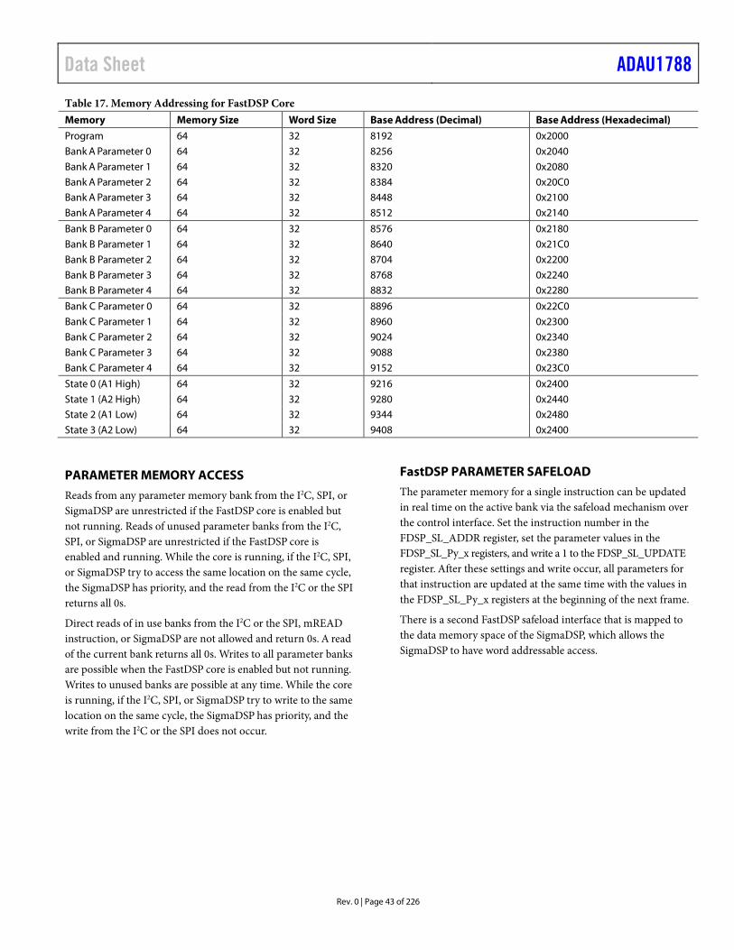
Data Sheet ADAU1788
Rev. 0 | Page 43 of 226
Table 17. Memory Addressing for FastDSP Core Memory Memory Size Word Size Base Address (Decimal) Base Address (Hexadecimal) Program 64 32 8192 0x2000 Bank A Parameter 0 64 32 8256 0x2040 Bank A Parameter 1 64 32 8320 0x2080 Bank A Parameter 2 64 32 8384 0x20C0 Bank A Parameter 3 64 32 8448 0x2100 Bank A Parameter 4 64 32 8512 0x2140 Bank B Parameter 0 64 32 8576 0x2180 Bank B Parameter 1 64 32 8640 0x21C0 Bank B Parameter 2 64 32 8704 0x2200 Bank B Parameter 3 64 32 8768 0x2240 Bank B Parameter 4 64 32 8832 0x2280 Bank C Parameter 0 64 32 8896 0x22C0 Bank C Parameter 1 64 32 8960 0x2300 Bank C Parameter 2 64 32 9024 0x2340 Bank C Parameter 3 64 32 9088 0x2380 Bank C Parameter 4 64 32 9152 0x23C0 State 0 (A1 High) 64 32 9216 0x2400 State 1 (A2 High) 64 32 9280 0x2440 State 2 (A1 Low) 64 32 9344 0x2480 State 3 (A2 Low) 64 32 9408 0x2400
PARAMETER MEMORY ACCESS Reads from any parameter memory bank from the I2C, SPI, or SigmaDSP are unrestricted if the FastDSP core is enabled but not running. Reads of unused parameter banks from the I2C, SPI, or SigmaDSP are unrestricted if the FastDSP core is enabled and running. While the core is running, if the I2C, SPI, or SigmaDSP try to access the same location on the same cycle, the SigmaDSP has priority, and the read from the I2C or the SPI returns all 0s.
Direct reads of in use banks from the I2C or the SPI, mREAD instruction, or SigmaDSP are not allowed and return 0s. A read of the current bank returns all 0s. Writes to all parameter banks are possible when the FastDSP core is enabled but not running. Writes to unused banks are possible at any time. While the core is running, if the I2C, SPI, or SigmaDSP try to write to the same location on the same cycle, the SigmaDSP has priority, and the write from the I2C or the SPI does not occur.
FastDSP PARAMETER SAFELOAD The parameter memory for a single instruction can be updated in real time on the active bank via the safeload mechanism over the control interface. Set the instruction number in the FDSP_SL_ADDR register, set the parameter values in the FDSP_SL_Py_x registers, and write a 1 to the FDSP_SL_UPDATE register. After these settings and write occur, all parameters for that instruction are updated at the same time with the values in the FDSP_SL_Py_x registers at the beginning of the next frame.
There is a second FastDSP safeload interface that is mapped to the data memory space of the SigmaDSP, which allows the SigmaDSP to have word addressable access.
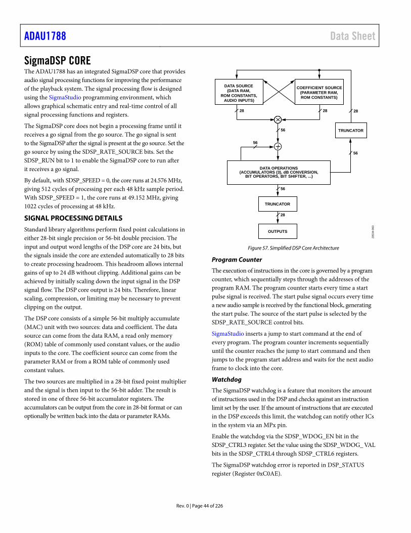
ADAU1788 Data Sheet
Rev. 0 | Page 44 of 226
SigmaDSP CORE The ADAU1788 has an integrated SigmaDSP core that provides audio signal processing functions for improving the performance of the playback system. The signal processing flow is designed using the SigmaStudio programming environment, which allows graphical schematic entry and real-time control of all signal processing functions and registers.
The SigmaDSP core does not begin a processing frame until it receives a go signal from the go source. The go signal is sent to the SigmaDSP after the signal is present at the go source. Set the go source by using the SDSP_RATE_SOURCE bits. Set the SDSP_RUN bit to 1 to enable the SigmaDSP core to run after it receives a go signal.
By default, with SDSP_SPEED = 0, the core runs at 24.576 MHz, giving 512 cycles of processing per each 48 kHz sample period. With SDSP_SPEED = 1, the core runs at 49.152 MHz, giving 1022 cycles of processing at 48 kHz.
SIGNAL PROCESSING DETAILS Standard library algorithms perform fixed point calculations in either 28-bit single precision or 56-bit double precision. The input and output word lengths of the DSP core are 24 bits, but the signals inside the core are extended automatically to 28 bits to create processing headroom. This headroom allows internal gains of up to 24 dB without clipping. Additional gains can be achieved by initially scaling down the input signal in the DSP signal flow. The DSP core output is 24 bits. Therefore, linear scaling, compression, or limiting may be necessary to prevent clipping on the output.
The DSP core consists of a simple 56-bit multiply accumulate (MAC) unit with two sources: data and coefficient. The data source can come from the data RAM, a read only memory (ROM) table of commonly used constant values, or the audio inputs to the core. The coefficient source can come from the parameter RAM or from a ROM table of commonly used constant values.
The two sources are multiplied in a 28-bit fixed point multiplier and the signal is then input to the 56-bit adder. The result is stored in one of three 56-bit accumulator registers. The accumulators can be output from the core in 28-bit format or can optionally be written back into the data or parameter RAMs.
COEFFICIENT SOURCE(PARAMETER RAM,ROM CONSTANTS)
DATA OPERATIONS(ACCUMULATORS (3), dB CONVERSION,
BIT OPERATORS, BIT SHIFTER, ...)
DATA SOURCE(DATA RAM,
ROM CONSTANTS,AUDIO INPUTS)
OUTPUTS
TRUNCATOR
TRUNCATOR56
56
56
28
28
2828
56
2053
4-06
3
Figure 57. Simplified DSP Core Architecture
Program Counter
The execution of instructions in the core is governed by a program counter, which sequentially steps through the addresses of the program RAM. The program counter starts every time a start pulse signal is received. The start pulse signal occurs every time a new audio sample is received by the functional block, generating the start pulse. The source of the start pulse is selected by the SDSP_RATE_SOURCE control bits.
SigmaStudio inserts a jump to start command at the end of every program. The program counter increments sequentially until the counter reaches the jump to start command and then jumps to the program start address and waits for the next audio frame to clock into the core.
Watchdog
The SigmaDSP watchdog is a feature that monitors the amount of instructions used in the DSP and checks against an instruction limit set by the user. If the amount of instructions that are executed in the DSP exceeds this limit, the watchdog can notify other ICs in the system via an MPx pin.
Enable the watchdog via the SDSP_WDOG_EN bit in the SDSP_CTRL3 register. Set the value using the SDSP_WDOG_ VAL bits in the SDSP_CTRL4 through SDSP_CTRL6 registers.
The SigmaDSP watchdog error is reported in DSP_STATUS register (Register 0xC0AE).

Data Sheet ADAU1788
Rev. 0 | Page 45 of 226
Features
The SigmaDSP core architecture is designed specifically for audio processing and, therefore, includes several features that maximize processing efficiency. Hardware accelerators, such as decibel conversion, trigonometric tables, and audio specific ROM constants provide improved processing power and simplified algorithm coding.
Numeric Formats
DSP systems commonly use a standard numeric format. Fractional numeric systems are specified by an AB format, where A is the number of bits to the left of the decimal point, and B is the number of bits to the right of the decimal point.
The ADAU1788 uses the Numeric Format 5.23 for both the parameter and data values.
Numeric Format 5.23
The linear range of the ADAU1788 numeric format is −16.0 to +16.0 − 1 LSB.
For example,
• 1000 0000 0000 0000 0000 0000 0000 = −16.0 • 1110 0000 0000 0000 0000 0000 0000 = −4.0 • 1111 1000 0000 0000 0000 0000 0000 = −1.0 • 1111 1110 0000 0000 0000 0000 0000 = −0.25 • 1111 1111 0011 0011 0011 0011 0011 = −0.1 • 1111 1111 1111 1111 1111 1111 1111 = +1 LSB below 0 • 0000 0000 0000 0000 0000 0000 0000 = +0 • 0000 0000 1100 1100 1100 1100 1101 = +0.1 • 0000 0010 0000 0000 0000 0000 0000 = +0.25 • 0000 1000 0000 0000 0000 0000 0000 = +1.0 • 0010 0000 0000 0000 0000 0000 0000 = +4.0 • 0111 1111 1111 1111 1111 1111 1111 = +16.0 − 1 LSB
The serial port accepts up to 24 bits on the input and is sign extended to the full 28 bits of the DSP core.
Programming
On power-up, the ADAU1788 must be configured with a clocking scheme and then loaded with register settings. After the codec signal path is set up, the DSP core can be programmed. With a 48 kHz sample rate, the internal clock rate is 49.152 MHz, resulting in 1024 instruction cycles per audio sample rate.
The device can be programmed using the SigmaStudio graphic tool provided by Analog Devices. No knowledge of writing line level DSP code is required. More information about SigmaStudio is available at www.analog.com/SigmaStudio.
READ/WRITE DATA FORMATS The read/write formats of the control port are byte oriented to allow ease of programming of common microcontrollers. To fit the data into a byte oriented format, 0s are added to the data fields before the MSB to extend the data-word to a full 8 bits. For example, 28-bit words written to the parameter RAM are preceded by four leading 0s to create a 32-bit (4-byte) word, and 39-bit words written to the program RAM are preceded by one leading 0 to create a 40-bit (5-byte) word. These zero padded data fields are appended to a 3-byte field that consists of a 7-bit chip address, a read/write bit, and a 16-bit RAM/register address. The control port knows how many data bytes to expect based on the address given in the first three bytes.
The total number of bytes for a single location write command can vary from one byte (for a control register write) to five bytes (for a program RAM write). Use burst mode to fill the contiguous register or RAM locations. A burst mode write begins by writing the address and data of the first RAM or register location to be written to. Rather than ending the control port transaction (by issuing a stop command in I2C mode or by bringing the SS signal high in SPI mode after the data-word), as in a single-address write, the next data-word can be written immediately without specifying its address. The ADAU1788 control port auto-increments the address of each write even across the boundaries of the different RAMs and registers. Burst mode is outlined in the respective control port sections.

ADAU1788 Data Sheet
Rev. 0 | Page 46 of 226
SOFTWARE SAFELOAD To update parameters in real time while avoiding pop and click noises on the output, the ADAU1788 uses a software safeload mechanism. The software safeload mechanism enables the SigmaDSP core to load new parameters into the RAM while guaranteeing that the parameters are not in use. The use of this mechanism prevents an undesirable condition where an instruction executes with a mix of old and new parameters.
SigmaStudio sets up the necessary code and parameters automatically for new projects. The safeload code, along with other initialization codes, fills the first 39 locations in the program RAM. The first eight parameter RAM locations (Address 0x0000 to Address 0x0007) are configured by default in SigmaStudio as described in Table 18.
Table 18. Software Safeload Parameter RAM Defaults Address (Hex) Function 0x0000 Modulo RAM size 0x0001 Safeload Data 1 0x0002 Safeload Data 2 0x0003 Safeload Data 3 0x0004 Safeload Data 4 0x0005 Safeload Data 5 0x0006 Safeload target address (offset of −1) 0x0007 Number of words to write/safeload trigger
Address 0x0000, which controls the modulo RAM size, is set by SigmaStudio and is based on the dynamic address generator mode of the project.
Parameter RAM Address 0x0001 to Address 0x0005 are the five data slots for storing the data for safe loading. The safeload parameter space contains five data slots by default because most standard signal processing algorithms have five parameters or less.
Address 0x0006 is the safeload target address in the RAM (with an offset of −1) parameter, which designates the first address to be written. If more than one word is written, the address increments automatically for each data-word. Up to five sequential parameter RAM locations can be updated with safeload during each audio frame. The target address offset of −1 is used
because the write address is calculated relative to the address of the data, which starts at Address 0x0001. Therefore, to update a parameter at Address 0x000A, the target address is 0x0009.
Address 0x0007 designates the number of words to be written to the RAM parameter during the safeload. A biquad filter uses all five safeload data addresses. A simple mono gain cell uses only one safeload data address. Writing to Address 0x0007 also triggers the safeload write to occur in the next audio frame.
The safeload mechanism is software based and executes once per audio frame. Therefore, take care when designing the communication protocol. A delay equal to or greater than the sampling period (the inverse of sampling frequency) is required between each safeload write. A sample rate of 48 kHz equates to a delay of at least 21 μs. If this delay is not observed, the downloaded data is corrupted.
FastDSP SAFELOAD There are five memory locations mapped to the data memory of the SigmaDSP that can be used to update the current bank parameters of a single instruction of the FastDSP.
The functionality of this is the same as the functionality of the FastDSP safeload via the control port (refer to the FastDSP Parameter Safeload section). The difference is that the parameters can be addressed on a 32-bit word basis, making the writes more efficient than reusing the control port fast load mechanism that is byte addressable. The parameters are also written to the FastDSP as soon as the frame executes, without needing to write a trigger bit. Table 19 lists the SigmaDSP assembler names for the functions used for safeload.
Table 19. SigmaDSP Safeload to the FastDSP Current Bank Name Function FDSP_SL_ADDR FastDSP safeload instruction number FDSP_SL_P0 FastDSP Safeload Parameter B0 FDSP_SL_P1 FastDSP Safeload Parameter B1 FDSP_SL_P2 FastDSP Safeload Parameter B2 FDSP_SL_P3 FastDSP Safeload Parameter A1 FDSP_SL_P4 FastDSP Safeload Parameter A2

Data Sheet ADAU1788
Rev. 0 | Page 47 of 226
PROGRAM RAM, PARAMETER RAM, AND DATA RAM The ADAU1788 address space encompasses a set of registers and three RAMs: program, parameter, and data. Table 20 shows the RAM map. The memory map from the perspective of the SigmaDSP is different than the mapping of the memories to the external control interface because internally within the SigmaDSP each word has its own address, while over the control interface, each byte has its own address. Additionally, the mapping of the memories to the external control interface is offset.
The program RAM and parameter RAM are not initialized on power-up and are in an unknown state until the RAMs are written to.
PROGRAM RAM The program RAM contains the 39-bit operation codes that are executed by the core. The SigmaStudio compiler calculates the instructions executed per frame for a given program and generates an error when this number exceeds the maximum allowable instructions per frame based on the sample rate of the signals in the core.
Because the end of a program contains a jump to start command, the unused program RAM space does not need to be filled with no operation (NOP) commands.
PARAMETER RAM The parameter RAM is 28-bits wide and occupies Address 0 (0x0000) to Address 1023 (0x3FFF). The data format of the parameter RAM is twos complement, 5.23, which means that the coefficients can range from +16.0 (minus 1 LSB) to −16.0, with 1.0 represented by the binary word 0000 1000 0000 0000 0000 0000 0000 or by the hexadecimal word 0x00 0x80 0x00 0x00.
The parameter RAM can be written to directly or with a safeload write. The direct write mode of operation is typically used during a completely new loading of the RAM using burst mode addressing to avoid any clicks or pops in the outputs. Although this mode can be used during program execution, there is no handshaking between the core and the control port, and the parameter RAM is unavailable to the DSP core during control writes, resulting in pops and clicks in the audio stream.
SigmaStudio automatically assigns the first eight positions to safeload parameters. Therefore, project specific parameters start at Address 0x0008.
The SDSP_RUN bit (Bit 0, Register 0xC081) must be set to 0 before writing to the parameter RAM.
DATA RAM The ADAU1788 data RAM stores audio data-words for processing, as well as certain run-time parameters. SigmaStudio provides the data and address information for writing to and reading from the data RAM. The ADAU1788 has 2048 words of data RAM available.
The SigmaStudio compiler manages the data RAM and indicates whether the number of addresses needed in the design exceeds the maximum number available.
Table 20. RAM SigmaDSP Internal Map and Read/Write Modes Memory Size (Words) Address Range Read Write Write Modes Parameter RAM 2048 × 28 0 to 2047 (0x0000 to 0x03FF) Yes Yes Direct, safeload Program RAM 2048 × 39 3072 to 4095 (0x0C00 to 0x13FF) Yes Yes Direct
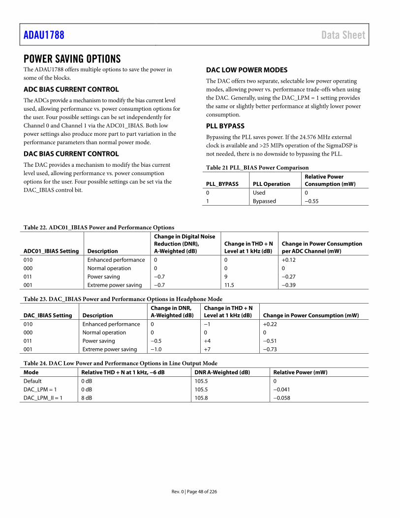
ADAU1788 Data Sheet
Rev. 0 | Page 48 of 226
POWER SAVING OPTIONS The ADAU1788 offers multiple options to save the power in some of the blocks.
ADC BIAS CURRENT CONTROL The ADCs provide a mechanism to modify the bias current level used, allowing performance vs. power consumption options for the user. Four possible settings can be set independently for Channel 0 and Channel 1 via the ADC01_IBIAS. Both low power settings also produce more part to part variation in the performance parameters than normal power mode.
DAC BIAS CURRENT CONTROL The DAC provides a mechanism to modify the bias current level used, allowing performance vs. power consumption options for the user. Four possible settings can be set via the DAC_IBIAS control bit.
DAC LOW POWER MODES The DAC offers two separate, selectable low power operating modes, allowing power vs. performance trade-offs when using the DAC. Generally, using the DAC_LPM = 1 setting provides the same or slightly better performance at slightly lower power consumption.
PLL BYPASS Bypassing the PLL saves power. If the 24.576 MHz external clock is available and >25 MIPs operation of the SigmaDSP is not needed, there is no downside to bypassing the PLL.
Table 21 PLL_BIAS Power Comparison
PLL_BYPASS PLL Operation Relative Power Consumption (mW)
0 Used 0 1 Bypassed −0.55
Table 22. ADC01_IBIAS Power and Performance Options
ADC01_IBIAS Setting Description
Change in Digital Noise Reduction (DNR), A-Weighted (dB)
Change in THD + N Level at 1 kHz (dB)
Change in Power Consumption per ADC Channel (mW)
010 Enhanced performance 0 0 +0.12 000 Normal operation 0 0 0 011 Power saving −0.7 9 −0.27 001 Extreme power saving −0.7 11.5 −0.39
Table 23. DAC_IBIAS Power and Performance Options in Headphone Mode
DAC_IBIAS Setting Description Change in DNR, A-Weighted (dB)
Change in THD + N Level at 1 kHz (dB) Change in Power Consumption (mW)
010 Enhanced performance 0 −1 +0.22 000 Normal operation 0 0 0 011 Power saving −0.5 +4 −0.51 001 Extreme power saving −1.0 +7 −0.73
Table 24. DAC Low Power and Performance Options in Line Output Mode Mode Relative THD + N at 1 kHz, −6 dB DNR A-Weighted (dB) Relative Power (mW) Default 0 dB 105.5 0 DAC_LPM = 1 0 dB 105.5 −0.041 DAC_LPM_II = 1 8 dB 105.8 −0.058

Data Sheet ADAU1788
Rev. 0 | Page 49 of 226
SigmaDSP CLOCK SPEED CONTROL By default, SDSP_SPEED is set to 0 and the SigmaDSP receives a 24.576 MHz clock. If the PLL is used and SDSP_SPEED is set to 1, the SigmaDSP receives a 49.152 MHz clock and is able to run twice as many instructions. If this extra processing power is not needed, keeping SDSP_SPEED = 0 saves power.
Table 25. SDSP_SPEED Power Comparison
SDSP_SPEED SigmaDSP Clock Rate (MHz)
Relative Power Consumption (mW)
1 49.152 0 0 24.576 −0.076
ASYNCHRONOUS SAMPLE RATE CONVERTERS LOW POWER MODES The ASRCs offer two separate, selectable low power operating modes. These modes allow power vs. performance trade-offs when using the ASRCs. Generally, if the data being sourced or sinked to the ASRCs is from or to the ADC or DAC using the ASRCx_LPM_II setting provides the lowest power consumption and does not degrade the performance of the converters.
Table 26. Input ASRC Power and Performance Options for 44.1 kHz to 48 kHz Conversion Mode THD + N at 1 kHz (dB) THD + N at 20 kHz DNR AW (dB) Relative Power per Channel (mW) Default 123 123 130 0 ASRCI_LPM = 1 120 118 130 −0.041 ASRCI_LPM_II = 1 112 108 130 −0.058
Table 27. Output ASRC Power and Performance Options for 48 kHz to 44.1 kHz Conversion Mode THD + N at 1 kHz (dB) THD + N at 20 kHz DNR AW (dB) Relative Power per Channel (mW) Default 123 123 130 0 ASRCO_LPM = 1 120 118 130 −0.045 ASRCO_LPM_II = 1 112 108 130 −0.070

ADAU1788 Data Sheet
Rev. 0 | Page 50 of 226
CONTROL PORT The ADAU1788 has a 4-wire SPI control port and a 2-wire I2C bus control port. Each port can set the memories and registers. The IC defaults to I2C mode but can be put into SPI control mode by pulling the SS pin low three times. When in I2C mode, the unused control pins determine the I2C device address. The D3 pin must be connected to DGND for the I2C/SPI operation.
The control port is capable of full read/write operation for all addressable memories and registers. Most signal processing parameters are controlled by writing new values to the parameter memories using the control port. Other functions, such as mute and input/output mode control, are programmed through the registers.
All addresses can be accessed in either single address mode or burst mode. The first byte (Byte 0) of a control port write contains the 7-bit IC address plus the R/W bit. The next two bytes (Byte 1 and Byte 2) are the 16-bit subaddress of the memory or register location within the ADAU1788. All subsequent bytes (starting with Byte 3) contain the data, such as the register, program, or parameter data. The exact formats for specific types of writes are shown in Figure 60 and Figure 61.
If large blocks of data must be downloaded to the ADAU1788 DSP cores, the output of the cores can be disabled, new data can be loaded, and the core can then be restarted. This restart is typically done during the booting sequence at start-up or when loading a new program into memory.
Registers and bits shown as reserved in the register map read back 0s.
The control port pins are multifunctional, depending on the mode in which the device is operating. Table 28 describes these multiple functions.
Table 28. Control Port Pin Functions Pin I2C Mode SPI Mode SCL/SCLK SCL—input SCLK—input SDA/MISO SDA—open-collector output MISO—output ADDR1/MOSI I2C Address Bit 1—input MOSI—input ADDR0/SS I2C Address Bit 0—input SS—input
BURST MODE COMMUNICATION Burst mode addressing, in which the subaddresses are automatically incremented at word boundaries, can be used for writing large amounts of data to contiguous memory locations. This increment happens automatically after a single-word write unless the control port communication is stopped (that is, a stop condition is issued for I2C, or SS is brought high for SPI). The registers and RAMs in the ADAU1788 range in width from one byte to five bytes, so the auto-increment feature knows the mapping between subaddresses and the word length of the destination register (or memory location).
Table 29. Control Pins Function Setup List
Mode IOVDD (V) I2C Address BCLK0 Pin SDATAO_0 Pin ADDR1/ MOSI Pin
ADDR0/ SS Pin
SCL/ SCLK Pin
SDA/ MISO Pin D3 Pin
Input 1.2 to 1.8 0x28 BCLK0 SDATAO_0 0 0 SCL SDA 0
I2C 1.2 to 1.8 0x29 BCLK0 SDATAO_0 0 1 SCL SDA 0 I2C 1.2 to 1.8 0x2A BCLK0 SDATAO_0 1 0 SCL SDA 0
I2C 1.2 to 1.8 0x2B BCLK0 SDATAO_0 1 1 SCL SDA 0
SPI 1.2 to 1.8 Not applicable BCLK0 SDATAO_0 MOSI SS SCLK MISO 0
Table 30. I2C/SPI Control Data Word Sizes and Address Ranges Base Address End Address Description Width per Address Write Modes Writes Needed for Update 0x0000 0x0F00 Reserved Not applicable Not applicable Not applicable 0x2000 0x3FFF SigmaDSP parameter RAM 8 Direct, safeload 4 0x5000 0x77FF SigmaDSP program RAM 8 Direct 5 0x7800 0x97FF SigmaDSP data RAM 8 Direct 4 0xC000 0xC0E1 Control registers 8 Direct 1 0xD000 0xD0FF FastDSP program 8 Direct 4 0xD100 0xDFFF FastDSP parameter 8 Direct safeload 4 0xE000 0xE3FF FastDSP state 8 Direct 4

Data Sheet ADAU1788
Rev. 0 | Page 51 of 226
READING AND WRITING TO MEMORIES All SigmaDSP and FastDSP memory locations are larger than a single byte. While each byte occupies a single address when communicating over a control interface (I2C or SPI), when writing to these memories, an entire memory word must be written starting with the lowest address and continuing sequentially to the highest address for a write to actually occur. Similarly, a read must begin at the lowest memory address. However, for reads, all locations must not be read. The mapping of bytes over the control interface is the most significant byte, or a memory location is written or read first, and the least significant byte is written or read last. The memories can be read or written in burst mode or single byte mode so that the proceeding requirements are met.
Table 31. Example Write to SigmaDSP Program RAM Word 0 Address Data 0x5000 Data, Bits[39:32] 0x5001 Data, Bits[31:24] 0x5002 Data, Bits[23:16] 0x5003 Data, Bits[15:8] 0x5004 Data, Bits[7:0], the memory is written to after this write
I2C PORT The ADAU1788 supports a 2-wire serial (I2C-compatible) microprocessor bus driving multiple peripherals. I2C uses two pins, serial data (SDA) and serial clock (SCL), to carry data between the ADAU1788 and the system I2C master controller. In I2C mode, the ADAU1788 is always a slave on the bus.
The device supports fast mode plus I2C operation, but for most bus capacitances, the SDA_MISO_DRIVE bit must be set to 1 to support these operating speeds.
Each slave device is recognized by a unique 7-bit device address. The ADAU1788 I2C address format is shown in Table 32. The LSB of this first byte sent from the I2C master sets either a read or write operation. Logic Level 1 corresponds to a read operation, and Logic Level 0 corresponds to a write operation.
Pin ADDR0 and Pin ADDR1 set the LSBs of the I2C address (see Table 33). Therefore, each ADAU1788 can be set to one of four unique addresses, allowing multiple ICs to exist on the same I2C bus without address contention. The 7-bit I2C addresses are shown in Table 33.
An I2C data transfer is always terminated by a stop condition.
Both SDA and SCL must have 2.0 kΩ pull-up resistors on the lines connected to these pins. The voltage on these signal lines cannot be higher than IOVDD.
Table 32. I2C Address Format Bit 6 Bit 5 Bit 4 Bit 3 Bit 2 Bit 1 Bit 0 0 1 0 1 0 ADDR1 ADDR0
Table 33. I2C Addresses ADDR1 (MOSI) ADDR0 (SS) Slave Address 0 0 0x28 0 1 0x29 1 0 0x2A 1 1 0x2B
Addressing
Initially, each device on the I2C bus is in an idle state and monitoring the SDA and SCL lines for a start condition and the proper address. The I2C master initiates a data transfer by establishing a start condition, defined by a high to low transition on SDA while SCL remains high, indicating that an address/ data stream follows. All devices on the bus respond to the start condition and shift the next eight bits (the 7-bit address plus the R/W bit) MSB first. The device that recognizes the transmitted address responds by pulling the data line low during the ninth clock pulse. This ninth bit is known as an acknowledge bit. All other devices withdraw from the bus at this point and return to the idle condition. The R/W bit determines the direction of the data. A Logic 0 on the LSB of the first byte indicates that the master writes information to the peripheral, whereas a Logic 1 indicates that the master reads information from the peripheral after writing the subaddress and repeating the start address. A data transfer takes place until a stop condition is encountered. A stop condition occurs when SDA transitions from low to high while SCL is held high. Figure 58 shows the timing of an I2C write, and Figure 59 shows an I2C read.
Stop and start conditions can be detected at any stage during the data transfer. If these conditions are asserted out of sequence with normal read and write operations, the ADAU1788 immediately jumps to the idle condition. During a given SCL high period, the user can only issue one start condition, one stop condition, or a single stop condition followed by a single start condition. A no-acknowledge condition is where the SDA line is not pulled low on the ninth clock pulse on SCL. If an invalid subaddress is issued by the user, the ADAU1788 issues an acknowledge, but no data write occurs, and a read returns zeros. If the highest subaddress location is reached while in write mode, the data for the invalid byte is not loaded to any subaddress register.

ADAU1788 Data Sheet
Rev. 0 | Page 52 of 226
R/W0
SCL
SDA
SDA(CONTINUED)
SCL(CONTINUED)
1 0 1 ADDR0ADDR10
START BYMASTER
FRAME 1CHIP ADDRESS BYTE
FRAME 2SUBADDRESS BYTE 1
FRAME 3SUBADDRESS BYTE 2
FRAME 4DATA BYTE 1
ACKNOWLEDGEBY ADAU1788
ACKNOWLEDGEBY ADAU1788
ACKNOWLEDGEBY ADAU1788
ACKNOWLEDGEBY ADAU1788
STOP BYMASTER
2053
4-06
4
Figure 58. I2C Write to ADAU1788 Clocking
R/W
SCL
SDA
SDA(CONTINUED)
SCL(CONTINUED)
SDA(CONTINUED)
SCL(CONTINUED)
START BYMASTER
FRAME 2SUBADDRESS BYTE 1
FRAME 3SUBADDRESS BYTE 2
FRAME 4CHIP ADDRESS BYTE
FRAME 1CHIP ADDRESS BYTE
FRAME 5READ DATA BYTE 1
FRAME 6READ DATA BYTE 2
ACKNOWLEDGEBY ADAU1788
ACKNOWLEDGEBY ADAU1788
ACKNOWLEDGEBY ADAU1788
ACKNOWLEDGEBY ADAU1788
ACKNOWLEDGEBY ADAU1788
STOP BYMASTER
ACKNOWLEDGEBY ADAU1788
REPEATEDSTART BY MASTER
R/W
ADDR0
ADDR0ADDR1
ADDR1
0 1 0 1 0
1 0 1 00
2053
4-06
5
Figure 59. I2C Read from ADAU1788 Clocking

Data Sheet ADAU1788
Rev. 0 | Page 53 of 226
I2C Read and Write Operations
Figure 60 shows the timing of a single-word write operation. Every ninth clock pulse, the ADAU1788 issues an acknowledge by pulling SDA low.
Figure 61 shows the timing of a burst mode write sequence. Figure 61 shows an example where the target destination words are two bytes, such as the program memory. The ADAU1788 knows to increment its subaddress register every two bytes because the requested subaddress corresponds to a register or memory area with a 2-byte word length.
The timing of a single-word read operation is shown in Figure 62. Note that the first R/W bit is 0, indicating a write operation because the subaddress still must be written to set up the internal address. After the ADAU1788 acknowledges the receipt of the subaddress, the master must issue a repeated start command, followed by the chip address byte with the R/W set to 1 (read), causing the ADAU1788 SDA to reverse and begin driving data
back to the master. The master then responds every ninth pulse with an acknowledge pulse to the ADAU1788.
Figure 63 shows the timing of a burst mode read sequence. Figure 63 shows an example where the target read words are two bytes. The ADAU1788 increments its subaddress every two bytes because the requested subaddress corresponds to a register or memory area with word lengths of two bytes. Other address ranges may have a variety of word lengths, ranging from one byte to four bytes. The ADAU1788 always decodes the subaddress and sets the auto-increment circuit so that the address increments after the appropriate number of bytes.
Figure 60 to Figure 63 use the following abbreviations:
• S is the start bit. • P is the stop bit. • AM is acknowledge by master. • AS is acknowledge by slave.
DATA BYTE 1 AS DATA BYTE 2 AS... DATA BYTE N PS I2C ADDRESS,R/W = 0 AS SUBADDRESS
HIGH AS SUBADDRESSLOW AS
2053
4-06
6
Figure 60. Single-Word I2C Write Format
DATA-WORD 1,BYTE 1
DATA-WORD 1, BYTE 2AS ASS I2C ADDRESS,
R/W = 0 AS SUBADDRESSHIGH AS SUBADDRESS
LOW AS ...DATA-WORD 2,BYTE 1
DATA-WORD 2 BYTE 2AS AS P
2053
4-06
7
Figure 61. Burst Mode I2C Write Format
S I2C ADDRESS,R/W = 0 AS SUBADDRESS
HIGH AS SUBADDRESSLOW AS S I2C ADDRESS,
R/W = 1 DATA BYTE 1 AM DATA BYTE 2 AM... DATA BYTE N PAS
2053
4-06
8
Figure 62. Single-Word I2C Read Format
S I2C ADDRESS,R/W = 0 AS SUBADDRESS
HIGH AS SUBADDRESSLOW AS S I2C ADDRESS,
R/W = 1DATA-WORD 1
BYTE 1 AM DATA-WORD 1BYTE 2 AM ... PAS
2053
4-06
9
Figure 63. Burst Mode I2C Read Format

ADAU1788 Data Sheet
Rev. 0 | Page 54 of 226
SPI PORT By default, the ADAU1788 is in I2C mode, but the device can be put in SPI control mode by pulling SS low three times by issuing three SPI writes, which are in turn ignored by the ADAU1788. The next (fourth) SPI write is then latched in the SPI port.
The SPI port uses a 4-wire interface, consisting of SS, SCLK, MOSI, and MISO signals, and is always a slave port. The SS signal must go low at the beginning of a transaction and high at the end of a transaction. The SCLK signal latches MOSI on a low to high transition. MISO data is shifted out of the ADAU1788 on the falling edge of SCLK and must be clocked to a receiving device, such as a microcontroller, on the SCLK rising edge. The MOSI signal carries the serial input data, and the MISO signal is the serial output data. The MISO signal remains tristated until a read operation is requested, allowing other SPI-compatible peripherals to share the same readback line.
All SPI transactions have the same basic format shown in Table 34. The timing diagrams for SPI write and SPI read are shown in Figure 64 and Figure 65, respectively. All data must be written MSB first. The ADAU1788 can only be taken out of SPI mode by pulling the PD pin low or by powering down the IC.
R/W
The first byte of an SPI transaction indicates whether the communication is a read or a write with the R/W bit. The LSB of this first byte determines whether the SPI transaction is a read (Logic Level 1) or a write (Logic Level 0).
Subaddress
The 16-bit subaddress word is decoded into a location in one of the memories or registers. This subaddress is the location of the appropriate memory location or register.
It is necessary to add an unused byte of zeros after the subaddress to effectively make the subaddress 24 bits with the actual address placed in the 16 MSBs.
Data Bytes
The number of data bytes varies according to the register or memory being accessed. During a burst mode write, an initial subaddress is written followed by a continuous sequence of data for consecutive memory and/or register locations.
A sample timing diagram for a single-write SPI operation to the parameter RAM is shown in Figure 64. A sample timing diagram of a single-read SPI operation is shown in Figure 65. The MISO pin goes from tristate to being driven at the beginning of Byte 3. In this example, Byte 0 to Byte 2 contain the addresses and the R/W bit and subsequent bytes carry the data.
Table 34. Generic SPI Word Format Byte 0 Byte 1 Byte 2 Byte 3 Byte 4 Byte 51 0000000, R/W Register/memory address, Bits[15:8] Register/memory address, Bits[7:0] Zeros, Bits[7:0] (dummy) Data Data 1 Continues to end of data.
SS
SCLK
MOSI BYTE 0 BYTE 1 BYTE 2 BYTE 3 BYTE 4
DATADUMMY DATAREGISTER ADDRESS 2053
4-07
0
Figure 64. SPI Write to ADAU1788 Clocking (Single-Write Mode)
SS
SCLK
MOSI
MISO
BYTE 0 BYTE 1 BYTE 2 BYTE 3
VALID DATA HIGH-ZHIGH-Z ZERO DATA
BYTE 4
DUMMY DATADUMMY DATAREGISTER ADDRESS
2053
4-07
1
Figure 65. SPI Read from ADAU1788 Clocking (Single-Read Mode)

Data Sheet ADAU1788
Rev. 0 | Page 55 of 226
MULTIPURPOSE PINS The ADAU1788 has eleven multipurpose (MPx) pins that can be used for serial data I/O, digital microphone inputs, clock outputs, PDM outputs, and interrupts. Each pin can be individually set to either its default or MPx setting. The function of each of these pins is set in using the MPx_MODE bits. By default, each pin is configured as its normal function.
When an MPx pin is set as a general-purpose input, the MPx pin can be read via all control interfaces via the GPIOx_IN bits, the pin can also be read and acted upon by the SigmaDSP core, and the pin can be used to conditionally execute instructions or trigger the compressor in the FastDSP. When an MPx pin is set as general-purpose output, the state of the pin can be set via all control interfaces using the GPIOx_OUT bits or by the SigmaDSP core. The GPIO maps to the corresponding MPx pin, for example, GPIO1 maps to BCLK_0/MP1.
Any MPx pin can be used as a master clock output. The rate of the master clock output is determined by the MCLKO_RATE bits. Multiple pins can be used as this function if desired.
Any MPx pin can be used to output the PDM clock or data signal for the PDM output interface.
Any MPx pin can be used to output the interrupt status from the two interrupt sources.
Table 35. Multipurpose Pin Functions MPx Pin Function1 Direction General-Purpose Input (GPI) In General-Purpose Output from GPIOx_OUT Bits
(GPO_REG) Out
General-Purpose Output from SigmaDSP (GPO_SDSP) Out MCLK Output (MCLKO) Out IRQ1 Output (IRQ1) Out IRQ2 Output (IRQ2) Out
1 These functions are enumeration options in Register 0xC08B through Register 0xC090 that any of the MPx pins can be set to.
Interrupts
Each multipurpose pin can be used to output one of two interrupts that have various sources when selected for this function. The sources for the interrupts are for DAC and ADC channels clipping, PLL locking or unlocking, input and output ASRCs locking or unlocking, the generic SigmaDSP interrupts, and the AVDD undervoltage warning. Each interrupt source can be individually masked with their respective IRQx_MASKx registers. Each interrupt output can be set to active low or active high output on the pin selected for the interrupt output via the IRQx_FUNC bits.
The status of each interrupt source can be read via the IRQ status registers (IRQx_STATUSx). When an interrupt source is masked, if that interrupt becomes true, the interrupt is shown in the interrupt status registers but does not cause the MPx pin (if set as IRQx) to show an interrupt. All sources of each interrupt are cleared via a write of 1 to the IRQx_CLEAR bits. The interrupt status bits are sticky, such that if an interrupt source becomes true, the status reads 1 until a clear occurs, even if that interrupt source is no longer true.
The SigmaDSP interrupts are initiated by the SigmaDSP writing to the SDSP_INTx bits.
Pin Controls
Each pin that can be used as a multipurpose pin has several control selections to set various setting. When the pin is used as an output, the drive strength can be selected at 2 mA, 4 mA, 8 mA, or 12 mA. In addition, a weak pull-up or pull-down can be selected. These settings are in their respective pin control register. These pin control settings affect the pins operation in both normal functional mode and when used in all multipurpose pin modes.

ADAU1788 Data Sheet
Rev. 0 | Page 56 of 226
SERIAL DATA PORT The serial data input and output port of the ADAU1788 can be set to accept or transmit data in a 2-channel format such as I2S or up to 16 channels in a time division multiplexing (TDM) stream to interface to external ADCs, DAC, DSPs, and system on chips (SOCs). Data is processed in twos complement, MSB first format. The left channel data field always precedes the right channel data field in 2-channel streams.
The serial data clocks do not need to be synchronous with the ADAU1788 master clock input, but the frame clock and bit clock must be synchronous to each other. The FSYNC_0 and BCLK_0 pins are used to clock both the serial input and output ports. The pins can also be used as a source to the PLL to provide the main chip clock. The serial port can be set to be either the master or the slave in a system. Because there is only one set of serial data clocks, the input and output of the port must always both be either master or slave.
The SPT0_SAI_MODE bits set whether the serial port is operating in stereo mode or TDM mode. In stereo modes, both edges of frame clock determine where data is placed, and the left channel maps to the output for Channel 0, while the right channel maps to the output for Channel 1. In TDM mode only, the rising edge of frame clock determine where data is placed. In TDM mode, each channel of data receives a slot that can be either 16, 24, or 32 BCLKs wide. The width of each slot is determined by the SPT0_SLOT_WIDTH bits.
The serial data control registers allow control of the clock polarity and the data input modes. The valid data formats are I2S (delay by 1), left justified (delay by 0), or right justified (delay by 8, 12, or 16 BCLKs). The delay indicates the number of bit clocks BCLKs from the rising/falling edge of frame clock FSYNC_0 where the MSB of the data is placed in stereo modes, and the number of bit clocks BCLKs from the rising of frame clock in TDM mode. In all modes except for the right justified mode, the serial port inputs an arbitrary number of bits up to a limit of 24. Extra bits do not cause an error, but the bits are ignored. The serial port can operate with an arbitrary number of bit clock BCLK_0 transitions in each frame clock frame.
When using a high bit clock rate (12.288 MHz or higher), it is recommended to increase the drive strength settings for the output signal pins. The high drive strength effectively speeds up the transition times of the waveforms, thereby improving the signal integrity of the clock and data lines. The drive strength can be set in the pad drive strength registers (Register 0xC094 through Register 0xC0A0).
Table 36 describes the proper serial port settings for standard audio data formats. More information about the settings in Table 36 can be found in the SPT0_CTRLx register descriptions.
The polarity of both frame clock and bit clock can be inverted via the SPT0_LRCLK_POL and SPT0_BCLK_POL bits. These bits do not need to be used to support the typical formats shown in Table 36. Setting either SPT0_LRCLK_POL or SPT0_BCLK_POL to 1 places an inverter at the input to the serial port on its respective signal. For example, while serial data and frame clock are normally sampled on the rising edge of bit clock, setting SPT0_BCLK_POL = 1 samples on the falling edge of bit clock.
Each serial port can be set to be a master, in which case BCLK_0 and FSYNC_0 are driven as outputs. The output rate and direction of these two signals are set via the SPT0_LRCLK_SRC and SPT0_BCLK_SRC bits. A bit clock rate higher than 24.576 MHz cannot be generated. Therefore, the settings of these registers that request this rate result in no bit clock.
Unused bit slots can be tristated so that multiple ICs can drive a single serial data bus, which is controlled via the SPT0_TRI_ STATE bit. For example, in a 32-bit TDM frame with 24-bit data, the eight unused bits are tristated. Inactive channels are also tristated for one full frame each. Serial output channels are disabled when the SPT0_OUT_ROUTEy bits are set to 0x3E. Note that the timing for serial data output changes based on the minimum IOVDD voltage. While the serial port can work for inputting a signal on SDATAI_0 for any IOVDD and bit clock rate within the specification, the delay on SDATAO_0 at 1.1 V excludes operating at higher bit clock rates.
Table 36. Serial Port Data Format Settings
Format Frame Clock Mode, Bit (SPT0_SAI_MODE)
Sets the Slot Width per Channel, Bit (SPT0_SLOT_WIDTH)1
Sets the MSB Position from Start of Frame Clock, Bit (SPT0_DATA_FORMAT)
I2S (See Figure 66) 0 (50 % duty cycle) XX 000 (One bit clock delay) Left Justified (See Figure 66) 0 XX 001 (No delay) Right Justified (See Figure 66) 0 XX 010 (delay by 8 bit clocks) 0 XX 011 (delay by 12 bit clocks) 0 XX 100 (delay by 16 bit clocks) TDM (See Figure 67) 1 (single bit clock wide pulse) XX 000 1 X = don’t care.

Data Sheet ADAU1788
Rev. 0 | Page 57 of 226
BCLK_0
FSYNC_0
SDATAx I2S
SDATAx_0LEFT JUSTIFIED
SDATAx_0RIGHT JUSTIFIED
LEFT CHANNEL
LEFT CHANNEL
LEFT CHANNEL
RIGHT CHANNEL
RIGHT CHANNEL
RIGHT CHANNEL
2053
4-07
3
Figure 66. Stereo Modes: I2S, Left Justified, and Right Justified Modes, 16 Bits to 24 Bits per Channel, Any Number of BCLKs Are Allowed
29
BCLK_0
FSYNC_0
SDATAx_0 30 31 0 1 2 3 25 26
CHANNEL 0 CHANNEL 7
27 28 29 30 31 0 41 2 3 26 27 28 29 30 31 0
2053
4-07
4
Figure 67. 8-Channel TDM Mode, Default Settings, Except SPT0_SAI_MODE = 1

ADAU1788 Data Sheet
Rev. 0 | Page 58 of 226
APPLICATIONS INFORMATION POWER SUPPLY BYPASS CAPACITORS Bypass each analog and digital power supply pin to its nearest appropriate ground pin with a single 0.1 μF capacitor. The connections to each side of the capacitor must be as short as possible, and the trace must be routed on a single layer with no vias. For maximum effectiveness, locate the capacitor equidistant from the power and ground pins or slightly closer to the power pin if equidistant placement is not possible. Thermal connections to the ground planes must be made on the far side of the capacitor.
Each supply signal on the board must also be bypassed with a single bulk capacitor (10 μF to 47 μF).
AVDD PIN
FROM AVDD
CAPACITOR
AGND PIN
TO AGND
2053
4-07
5
Figure 68. Recommended Power Supply Bypass Capacitor Layout
LAYOUT The HPVDD supply is for the headphone amplifiers. If the headphone amplifiers are enabled, the PCB trace to this pin must be wider than the traces to other pins to increase the current carrying capacity. A wider trace must also be used for the headphone output lines.
GROUNDING Use a single ground plane in the application layout. Place the components in the analog signal path away from the digital signals.
PCB STACKUP Figure 69 shows the PCB stackup.
6 LAYER CONSTRUCTION DETAILSCALE: NONE
SILKSCREEN AND SOLDER MASK (0.8 MIL THICK)VIA L1 TO L4
0.062 ± 0.005
VIA L1 TO L6 LAYER 1 TOP SIDE 1.5OZ CU FINISHED (2 MIL THICK)LAMINATE (8.7 MIL THICK)LAYER 2 GROUND PLANE CU (0.6 MIL THICK)CORE (8 MIL THICK)LAYER 3 POWER PLANE 1 CU (0.6 MIL THICK)PREPREG (8.45 MIL THICK)LAYER 4 SIGNAL (CU 0.6 MIL THICK)PREPREG (3.9 MIL THICK)LAYER 5 BLANK (NO COPPER)PREPREG (8.45 MIL THICK)LAYER 5 (CU 0.6 MIL THICK)CORE (8 MIL THICK)LAYER 5 (GROUND PLANE CU 0.6 MIL THICK)PREPREG (8.7 MIL THICK)LAYER 6 BOTTOM SIDE 1.5 0Z CU FINISHED (2 MIL THICK)SCREEN AND SOLDER MASK 0.8 MIL THICK 20
534-
171
Figure 69. PCB Stackup

Data Sheet ADAU1788
Rev. 0 | Page 59 of 226
REGISTER SUMMARY Table 37. Register Summary Reg. (Hex.) Name Bits Bit 7 Bit 6 Bit 5 Bit 4 Bit 3 Bit 2 Bit 1 Bit 0 Reset R/W C000 VENDOR_
ID [7:0] VENDOR 0x41 R
C001 DEVICE_ ID1
[7:0] DEVICE1 0x17 R
C002 DEVICE_ ID2
[7:0] DEVICE2 0x87 R
C003 REVISION [7:0] REV 0x01 R C004 ADC_
DAC_ HP_PWR
[7:0] RESERVED PB0_EN RESERVED ADC1_EN ADC0_EN 0x00 R/W
C005 PLL_MB_ PGA_PWR
[7:0] RESERVED PGA1_EN PGA0_EN MBIAS1_ EN
MBIAS0_ EN
XTAL_EN PLL_EN 0x02 R/W
C006 DMIC_ PWR
[7:0] RESERVED DMIC3_ EN
DMIC2_ EN
DMIC1_EN DMIC0_EN 0x00 R/W
C007 SAI_CLK_ PWR
[7:0] PDM1_EN PDM0_EN DMIC_ CLK1_EN
DMIC_CLK0_EN RESERVED SPT0_ OUT_EN
SPT0_IN_EN 0x00 R/W
C008 DSP_PWR [7:0] RESERVED SDSP_EN RESERVED FDSP_EN 0x00 R/W C009 ASRC_
PWR [7:0] ASRCO3_
EN ASRCO2_ EN
ASRCO1_EN ASRCO0_EN ASRCI3_ EN
ASRCI2_ EN
ASRCI1_EN ASRCI0_EN 0x00 R/W
C00A FINT_ PWR
[7:0] FINT7_EN FINT6_EN FINT5_EN FINT4_EN FINT3_ EN
FINT2_EN FINT1_EN FINT0_EN 0x00 R/W
C00B FDEC_ PWR
[7:0] FDEC7_EN FDEC6_EN FDEC5_EN FDEC4_EN FDEC3_ EN
FDEC2_ EN
FDEC1_EN FDEC0_EN 0x00 R/W
C00C KEEPS [7:0] RESERVED CM_KEEP_ALIVE RESERVED KEEP_SDSP KEEP_FDSP 0x10 R/W C00D CHIP_
PWR [7:0] RESERVED DLDO_CTRL RESERVED CM_
STARTUP_ OVER
MASTER_ BLOCK_EN
POWER_EN 0x10 R/W
C00E CLK_ CTRL1
[7:0] SYNC_SOURCE PLL_BYPASS PLL_TYPE XTAL_ MODE
PLL_SOURCE 0xC8 R/W
C00F CLK_ CTRL2
[7:0] RESERVED PLL_INPUT_PRESCALER 0x00 R/W
C010 CLK_ CTRL3
[7:0] RESERVED PLL_INTEGER_DIVIDER[12:8] 0x00 R/W
C011 CLK_ CTRL4
[7:0] PLL_INTEGER_DIVIDER[7:0] 0x02 R/W
C012 CLK_ CTRL5
[7:0] PLL_NUMERATOR[15:8] 0x00 R/W
C013 CLK_ CTRL6
[7:0] PLL_NUMERATOR[7:0] 0x00 R/W
C014 CLK_ CTRL7
[7:0] PLL_DENOMINATOR[15:8] 0x00 R/W
C015 CLK_ CTRL8
[7:0] PLL_DENOMINATOR[7:0] 0x00 R/W
C016 CLK_ CTRL9
[7:0] RESERVED PLL_ UPDATE
0x00 R/W
C017 ADC_ CTRL1
[7:0] RESERVED ADC01_ DEC_ ORDER
ADC01_FS 0x22 R/W
C018 ADC_ CTRL2
[7:0] RESERVED ADC01_IBIAS 0x00 R/W
C019 ADC_ CTRL3
[7:0] RESERVED ADC1_ HPF_EN
ADC0_ HPF_EN
0x00 R/W
C01A ADC_ CTRL4
[7:0] RESERVED ADC_ VOL_ZC
ADC_ VOL_LINK
ADC_HARD_VOL RESERVED ADC01_ FCOMP
0x40 R/W
C01B ADC_ CTRL5
[7:0] RESERVED DIFF_INPUT ADC_AIN_CHRG_TIME 0x26 R/W
C01C ADC_ MUTES
[7:0] RESERVED ADC1_MUTE ADC0_MUTE 0x00 R/W
C01D ADC0_ VOL
[7:0] ADC0_VOL 0x40 R/W
C01E ADC1_ VOL
[7:0] ADC1_VOL 0x40 R/W

ADAU1788 Data Sheet
Rev. 0 | Page 60 of 226
Reg. (Hex.) Name Bits Bit 7 Bit 6 Bit 5 Bit 4 Bit 3 Bit 2 Bit 1 Bit 0 Reset R/W C021 PGA0_
CTRL1 [7:0] PGA0_
SLEW_DIS PGA0_ BOOST
PGA0_GAIN[10:5] 0x00 R/W
C022 PGA0_ CTRL2
[7:0] RESERVED PGA0_GAIN[4:0] 0x00 R/W
C023 PGA1_ CTRL1
[7:0] PGA1_ SLEW_DIS
PGA1_ BOOST
PGA1_GAIN[10:5] 0x00 R/W
C024 PGA1_ CTRL2
[7:0] RESERVED PGA1_GAIN[4:0] 0x00 R/W
C029 PGA_ CTRL
[7:0] RESERVED PGA_GAIN_LINK RESERVED PGA_SLEW_RATE 0x00 R/W
C02A MBIAS_ CTRL
[7:0] RESERVED MBIAS_IBIAS RESERVED MBIAS1_ LEVEL
MBIAS0_ LEVEL
0x00 R/W
C02B DMIC_ CTRL1
[7:0] RESERVED DMIC_CLK1_RATE RESERVED DMIC_CLK0_RATE 0x33 R/W
C02C DMIC_ CTRL2
[7:0] DMIC01_ MAP
DMIC01_ EDGE
DMIC01_ FCOMP
DMIC01_ DEC_ORDER
DMIC01_ HPF_EN
DMIC01_FS 0x01 R/W
C02D DMIC_ CTRL3
[7:0] DMIC23_ MAP
DMIC23_ EDGE
DMIC23_ FCOMP
DMIC23_ DEC_ORDER
DMIC23_ HPF_EN
DMIC23_FS 0x01 R/W
C030 DMIC_ CTRL6
[7:0] RESERVED DMIC_ VOL_ZC
DMIC_ VOL_LINK
DMIC_ HARD_VOL
0x04 R/W
C031 DMIC_ MUTES
[7:0] RESERVED DMIC3_ MUTE
DMIC2_ MUTE
DMIC1_MUTE DMIC0_ MUTE
0x00 R/W
C032 DMIC_ VOL0
[7:0] DMIC0_VOL 0x40 R/W
C033 DMIC_ VOL1
[7:0] DMIC1_VOL 0x40 R/W
C034 DMIC_ VOL2
[7:0] DMIC2_VOL 0x40 R/W
C035 DMIC_ VOL3
[7:0] DMIC3_VOL 0x40 R/W
C03A DAC_ CTRL1
[7:0] DAC_ MORE_ FILT
DAC_LPM DAC_IBIAS DAC_ FCOMP
DAC_FS 0x02 R/W
C03B DAC_ CTRL2
[7:0] RESERVED DAC0_ MUTE
RESERVED DAC0_ HPF_EN
DAC_ LPM_II
DAC_ VOL_ZC
DAC_ HARD_VOL
RESERVED 0xC4 R/W
C03C DAC_ VOL0
[7:0] DAC0_VOL 0x40 R/W
C03E DAC_ ROUTE0
[7:0] RESERVED DAC0_ROUTE 0x00 R/W
C040 HP_ CTRL
[7:0] RESERVED HP0_MODE 0x00 R/W
C041 FDEC_ CTRL1
[7:0] RESERVED FDEC01_OUT_FS RESERVED FDEC01_IN_FS 0x25 R/W
C042 FDEC_ CTRL2
[7:0] RESERVED FDEC23_OUT_FS RESERVED FDEC23_IN_FS 0x25 R/W
C043 FDEC_ CTRL3
[7:0] RESERVED FDEC45_OUT_FS RESERVED FDEC45_IN_FS 0x25 R/W
C044 FDEC_ CTRL4
[7:0] RESERVED FDEC67_OUT_FS RESERVED FDEC67_IN_FS 0x25 R/W
C045 FDEC_ ROUTE0
[7:0] RESERVED FDEC0_ROUTE 0x00 R/W
C046 FDEC_ ROUTE1
[7:0] RESERVED FDEC1_ROUTE 0x00 R/W
C047 FDEC_ ROUTE2
[7:0] RESERVED FDEC2_ROUTE 0x00 R/W
C048 FDEC_ ROUTE3
[7:0] RESERVED FDEC3_ROUTE 0x00 R/W
C049 FDEC_ ROUTE4
[7:0] RESERVED FDEC4_ROUTE 0x00 R/W
C04A FDEC_ ROUTE5
[7:0] RESERVED FDEC5_ROUTE 0x00 R/W
0xC04B FDEC_ ROUTE6
[7:0] RESERVED FDEC6_ROUTE 0x00 R/W
C04C FDEC_ ROUTE7
[7:0] RESERVED FDEC7_ROUTE 0x00 R/W

Data Sheet ADAU1788
Rev. 0 | Page 61 of 226
Reg. (Hex.) Name Bits Bit 7 Bit 6 Bit 5 Bit 4 Bit 3 Bit 2 Bit 1 Bit 0 Reset R/W C04D FINT_
CTRL1 [7:0] RESERVED FINT01_OUT_FS RESERVED FINT01_IN_FS 0x52 R/W
C04E FINT_ CTRL2
[7:0] RESERVED FINT23_OUT_FS RESERVED FINT23_IN_FS 0x52 R/W
C04F FINT_ CTRL3
[7:0] RESERVED FINT45_OUT_FS RESERVED FINT45_IN_FS 0x52 R/W
C050 FINT_ CTRL4
[7:0] RESERVED FINT67_OUT_FS RESERVED FINT67_IN_FS 0x52 R/W
C051 FINT_ ROUTE0
[7:0] RESERVED FINT0_ROUTE 0x00 R/W
C052 FINT_ ROUTE1
[7:0] RESERVED FINT1_ROUTE 0x00 R/W
C053 FINT_ ROUTE2
[7:0] RESERVED FINT2_ROUTE 0x00 R/W
C054 FINT_ ROUTE3
[7:0] RESERVED FINT3_ROUTE 0x00 R/W
C055 FINT_ ROUTE4
[7:0] RESERVED FINT4_ROUTE 0x00 R/W
C056 FINT_ ROUTE5
[7:0] RESERVED FINT5_ROUTE 0x00 R/W
C057 FINT_ ROUTE6
[7:0] RESERVED FINT6_ROUTE 0x00 R/W
C058 FINT_ ROUTE7
[7:0] RESERVED FINT7_ROUTE 0x00 R/W
C059 ASRCI_ CTRL
[7:0] ASRCI_ MORE_FILT
ASRCI_ VFILT
ASRCI_LPM RESERVED ASRCI_ LPM_II
ASRCI_OUT_FS 0x02 R/W
C05A ASRCI_ ROUTE01
[7:0] ASRCI1_ROUTE ASRCI0_ROUTE 0x00 R/W
C05B ASRCI_ ROUTE23
[7:0] ASRCI3_ROUTE ASRCI2_ROUTE 0x00 R/W
C05C ASRCO_ CTRL
[7:0] ASRCO_ MORE_FILT
ASRCO_ VFILT
ASRCO_ LPM
RESERVED ASRCO_ LPM_II
ASRCO_IN_FS 0x02 R/W
C05D ASRCO_ ROUTE0
[7:0] RESERVED ASRCO0_ROUTE 0x00 R/W
C05E ASRCO_ ROUTE1
[7:0] RESERVED ASRCO1_ROUTE 0x00 R/W
C05F ASRCO_ ROUTE2
[7:0] RESERVED ASRCO2_ROUTE 0x00 R/W
C060 ASRCO_ ROUTE3
[7:0] RESERVED ASRCO3_ROUTE 0x00 R/W
C061 FDSP_ RUN
[7:0] RESERVED FDSP_RUN 0x00 R/W
C062 FDSP_ CTRL1
[7:0] FDSP_RAMP_RATE FDSP_ ZERO_ STATE
FDSP_ RAMP_ MODE
FDSP_BANK_SEL 0x70 R/W
C063 FDSP_ CTRL2
[7:0] RESERVED FDSP_LAMBDA 0x3F R/W
C064 FDSP_ CTRL3
[7:0] RESERVED FDSP_ COPY_CB
FDSP_COPY_CA FDSP_ COPY_BC
FDSP_ COPY_BA
FDSP_ COPY_AC
FDSP_ COPY_AB
0x00 W
C065 FDSP_ CTRL4
[7:0] RESERVED FDSP_EXP_ ATK_SPEED
FDSP_RATE_SOURCE 0x00 R/W
C066 FDSP_ CTRL5
[7:0] FDSP_RATE_DIV[15:8] 0x00 R/W
C067 FDSP_ CTRL6
[7:0] FDSP_RATE_DIV[7:0] 0x7F R/W
C068 FDSP_ CTRL7
[7:0] RESERVED FDSP_MOD_N 0x00 R/W
C069 FDSP_ CTRL8
[7:0] FDSP_ REG_ COND7
FDSP_ REG_ COND6
FDSP_REG_ COND5
FDSP_REG_COND4 FDSP_ REG_ COND3
FDSP_ REG_ COND2
FDSP_REG_ COND1
FDSP_REG_ COND0
0x00 R/W
C06A FDSP_ SL_ADDR
[7:0] RESERVED FDSP_SL_ADDR 0x00 R/W
C06B FDSP_SL_ P0_3
[7:0] FDSP_SL_P0[31:24] 0x00 R/W
C06C FDSP_SL_ P0_2
[7:0] FDSP_SL_P0[23:16] 0x00 R/W
C06D FDSP_SL_ P0_1
[7:0] FDSP_SL_P0[15:8] 0x00 R/W

ADAU1788 Data Sheet
Rev. 0 | Page 62 of 226
Reg. (Hex.) Name Bits Bit 7 Bit 6 Bit 5 Bit 4 Bit 3 Bit 2 Bit 1 Bit 0 Reset R/W C06E FDSP_SL_
P0_0 [7:0] FDSP_SL_P0[7:0] 0x00 R/W
C06F FDSP_SL_ P1_3
[7:0] FDSP_SL_P1[31:24] 0x00 R/W
C070 FDSP_SL_ P1_2
[7:0] FDSP_SL_P1[23:16] 0x00 R/W
C071 FDSP_SL_ P1_1
[7:0] FDSP_SL_P1[15:8] 0x00 R/W
C072 FDSP_SL_ P1_0
[7:0] FDSP_SL_P1[7:0] 0x00 R/W
C073 FDSP_SL_ P2_3
[7:0] FDSP_SL_P2[31:24] 0x00 R/W
C074 FDSP_SL_ P2_2
[7:0] FDSP_SL_P2[23:16] 0x00 R/W
C075 FDSP_SL_ P2_1
[7:0] FDSP_SL_P2[15:8] 0x00 R/W
C076 FDSP_SL_ P2_0
[7:0] FDSP_SL_P2[7:0] 0x00 R/W
C077 FDSP_SL_ P3_3
[7:0] FDSP_SL_P3[31:24] 0x00 R/W
C078 FDSP_SL_ P3_2
[7:0] FDSP_SL_P3[23:16] 0x00 R/W
C079 FDSP_SL_ P3_1
[7:0] FDSP_SL_P3[15:8] 0x00 R/W
C07A FDSP_SL_ P3_0
[7:0] FDSP_SL_P3[7:0] 0x00 R/W
C07B FDSP_SL_ P4_3
[7:0] FDSP_SL_P4[31:24] 0x00 R/W
C07C FDSP_SL_ P4_2
[7:0] FDSP_SL_P4[23:16] 0x00 R/W
C07D FDSP_SL_ P4_1
[7:0] FDSP_SL_P4[15:8] 0x00 R/W
C07E FDSP_SL_ P4_0
[7:0] FDSP_SL_P4[7:0] 0x00 R/W
C07F FDSP_SL_ UPDATE
[7:0] RESERVED FDSP_SL_ UPDATE
0x00 W
C080 SDSP_ CTRL1
[7:0] RESERVED SDSP_SPEED SDSP_RATE_SOURCE 0x00 R/W
C081 SDSP_ CTRL2
[7:0] RESERVED SDSP_RUN 0x00 R/W
C082 SDSP_ CTRL3
[7:0] RESERVED SDSP_WDOG_ MUTE
RESERVED SDSP_ WDOG_EN
0x00 R/W
C083 SDSP_ CTRL4
[7:0] SDSP_WDOG_VAL[23:16] 0x00 R/W
C084 SDSP_ CTRL5
[7:0] SDSP_WDOG_VAL[15:8] 0x00 R/W
C085 SDSP_ CTRL6
[7:0] SDSP_WDOG_VAL[7:0] 0x00 R/W
C086 SDSP_ CTRL7
[7:0] RESERVED SDSP_MOD_DATA_MEM[11:8] 0x07 R/W
C087 SDSP_ CTRL8
[7:0] SDSP_MOD_DATA_MEM[7:0] 0xF4 R/W
C088 SDSP_ CTRL9
[7:0] SDSP_RATE_DIV[15:8] 0x07 R/W
C089 SDSP_ CTRL10
[7:0] SDSP_RATE_DIV[7:0] 0xFF R/W
C08A SDSP_ CTRL11
[7:0] RESERVED SDSP_ INT3
SDSP_ INT2
SDSP_INT1 SDSP_INT0 0x00 W
C08B MP_ CTRL1
[7:0] MP1_MODE MP0_MODE 0x00 R/W
C08C MP_ CTRL2
[7:0] MP3_MODE MP2_MODE 0x00 R/W
C08D MP_ CTRL3
[7:0] MP5_MODE MP4_MODE 0x00 R/W
C08E MP_ CTRL4
[7:0] MP7_MODE MP6_MODE 0x00 R/W

Data Sheet ADAU1788
Rev. 0 | Page 63 of 226
Reg. (Hex.) Name Bits Bit 7 Bit 6 Bit 5 Bit 4 Bit 3 Bit 2 Bit 1 Bit 0 Reset R/W C08F MP_
CTRL5 [7:0] MP9_MODE MP8_MODE 0x00 R/W
C090 MP_ CTRL6
[7:0] RESERVED MP10_MODE 0x00 R/W
C091 MP_ CTRL7
[7:0] RESERVED MCLKO_RATE RESERVED GPI_DB 0x10 R/W
C092 MP_ CTRL8
[7:0] GPIO7_ OUT
GPIO6_ OUT
GPIO5_OUT GPIO4_OUT GPIO3_ OUT
GPIO2_ OUT
GPIO1_OUT GPIO0_OUT 0x00 R/W
C093 MP_ CTRL9
[7:0] RESERVED GPIO10_ OUT
GPIO9_OUT GPIO8_OUT 0x00 R/W
C094 FSYNC0_ CTRL
[7:0] RESERVED FSYNC0_ PULL_SEL
FSYNC0_ PULL_EN
RESERVED FSYNC0_ SLEW
FSYNC0_DRIVE 0x05 R/W
C095 BCLK0_ CTRL
[7:0] RESERVED BCLK0_ PULL_SEL
BCLK0_ PULL_EN
RESERVED BCLK0_ SLEW
BCLK0_DRIVE 0x05 R/W
C096 SDATAO0_ CTRL
[7:0] RESERVED SDATAO0_ SLEW
RESERVED SDATAO0_ DRIVE
0x04 R/W
C097 SDATAI0_ CTRL
[7:0] RESERVED SDATAI0_ PULL_SEL
SDATAI0_ PULL_EN
RESERVED SDATAI0_ SLEW
SDATAI0_DRIVE 0x05 R/W
C098 MP3_ CTRL
[7:0] RESERVED MP3_ PULL_SEL
MP3_PULL_EN RESERVED MP3_ SLEW
MP3_DRIVE 0x05 R/W
C099 MP4_ CTRL
[7:0] RESERVED MP4_ PULL_SEL
MP4_PULL_EN RESERVED MP4_ SLEW
MP4_DRIVE 0x05 R/W
C09A MP5_ CTRL
[7:0] RESERVED MP5_ PULL_SEL
MP5_PULL_EN RESERVED MP5_ SLEW
MP5_DRIVE 0x05 R/W
C09B MP6_ CTRL
[7:0] RESERVED MP6_ PULL_SEL
MP6_PULL_EN RESERVED MP6_ SLEW
MP6_DRIVE 0x05 R/W
C09C DMIC_ CLK0_ CTRL
[7:0] RESERVED DMIC_ CLK0_ PULL_SEL
DMIC_CLK0_ PULL_EN
RESERVED DMIC_ CLK0_ SLEW
DMIC_CLK0_DRIVE 0x05 R/W
C09D DMIC_ CLK1_ CTRL
[7:0] RESERVED DMIC_ CLK1_ PULL_SEL
DMIC_CLK1_ PULL_EN
RESERVED DMIC_ CLK1_ SLEW
DMIC_CLK1_DRIVE 0x05 R/W
C09E DMIC01_ CTRL
[7:0] RESERVED DMIC01_ PULL_SEL
DMIC01_PULL_EN RESERVED DMIC01_ SLEW
DMIC01_DRIVE 0x05 R/W
C09F DMIC23_ CTRL
[7:0] RESERVED DMIC23_ PULL_SEL
DMIC23_PULL_EN RESERVED DMIC23_ SLEW
DMIC23_DRIVE 0x05 R/W
C0A0 I2C_SPI_ CTRL
[7:0] RESERVED SCL_SCLK_ DRIVE
SDA_ MISO_ DRIVE
0x00 R/W
C0A1 IRQ_ CTRL1
[7:0] RESERVED IRQ2_FUNC IRQ1_FUNC RESERVED IRQ2_ CLEAR
IRQ1_ CLEAR
0x00 R/W
C0A2 IRQ1_ MASK1
[7:0] RESERVED IRQ1_ADC1_ CLIP_MASK
IRQ1_ADC0_ CLIP_MASK
RESERVED IRQ1_ DAC0_ CLIP_ MASK
0xF3 R/W
C0A3 IRQ1_ MASK2
[7:0] IRQ1_ ASRCO_ UNLOCKED_ MASK
IRQ1_ ASRCO_ LOCKED_ MASK
IRQ1_ASRCI_ UNLOCKED_ MASK
IRQ1_ASRCI_ LOCKED_MASK
IRQ1_ PRAMP_ MASK
IRQ1_ AVDD_ UVW_ MASK
IRQ1_PLL_ UNLOCKED_ MASK
IRQ1_PLL_ LOCKED_ MASK
0xFF R/W
C0A4 IRQ1_ MASK3
[7:0] RESERVED IRQ1_POWER_UP_ COMPLETE_ MASK
IRQ1_ SDSP3_ MASK
IRQ1_ SDSP2_ MASK
IRQ1_ SDSP1_ MASK
IRQ1_ SDSP0_ MASK
0x1F R/W
C0A5 IRQ2_ MASK1
[7:0] RESERVED IRQ2_ADC1_ CLIP_MASK
IRQ2_ADC0_ CLIP_MASK
RESERVED IRQ2_ DAC0_ CLIP_ MASK
0xF3 R/W
C0A6 IRQ2_ MASK2
[7:0] IRQ2_ ASRCO_ UNLOCKED_ MASK
IRQ2_ ASRCO_ LOCKED_ MASK
IRQ2_ASRCI_ UNLOCKED_ MASK
IRQ2_ASRCI_ LOCKED_MASK
IRQ2_ PRAMP_ MASK
IRQ2_ AVDD_ UVW_ MASK
IRQ2_PLL_ UNLOCKED_ MASK
IRQ2_PLL_ LOCKED_ MASK
0xFF R/W
C0A7 IRQ2_ MASK3
[7:0] RESERVED IRQ2_POWER_ UP_COMPLETE_ MASK
IRQ2_ SDSP3_ MASK
IRQ2_ SDSP2_ MASK
IRQ2_ SDSP1_MASK
IRQ2_ SDSP0_ MASK
0x1F R/W
C0A8 RESETS [7:0] RESERVED SOFT_RESET RESERVED SOFT_ FULL_ RESET
0x00 W
C0A9 READ_ LAMBDA
[7:0] RESERVED FDSP_CURRENT_LAMBDA 0x3F R

ADAU1788 Data Sheet
Rev. 0 | Page 64 of 226
Reg. (Hex.) Name Bits Bit 7 Bit 6 Bit 5 Bit 4 Bit 3 Bit 2 Bit 1 Bit 0 Reset R/W C0AA STATUS1 [7:0] RESERVED ADC1_CLIP ADC0_CLIP RESERVED DAC0_
CLIP 0x00 R
C0AB STATUS2 [7:0] POWER_UP_ COMPLETE
SYNC_LOCK RESERVED SPT0_LOCK ASRCO_ LOCK
ASRCI_ LOCK
AVDD_ UVW
PLL_LOCK 0x00 R
C0AC GPI1 [7:0] GPIO7_IN GPIO6_IN GPIO5_IN GPIO4_IN GPIO3_IN GPIO2_IN GPIO1_IN GPIO0_IN 0x00 R C0AD GPI2 [7:0] RESERVED GPIO10_IN GPIO9_IN GPIO8_IN 0x00 R C0AE DSP_
STATUS [7:0] RESERVED SDSP_
WDOG_ ERROR
0x00 R
C0AF IRQ1_ STATUS1
[7:0] RESERVED IRQ1_ADC1_ CLIP
IRQ1_ADC0_CLIP RESERVED IRQ1_ DAC0_ CLIP
0x00 R
C0B0 IRQ1_ STATUS2
[7:0] IRQ1_ ASRCO_ UNLOCKED
IRQ1_ ASRCO_ LOCKED
IRQ1_ASRCI_ UNLOCKED
IRQ1_ASRCI_ LOCKED
IRQ1_ PRAMP
IRQ1_ AVDD_ UVW
IRQ1_PLL_ UNLOCKED
IRQ1_PLL_ LOCKED
0x00 R
C0B1 IRQ1_ STATUS3
[7:0] RESERVED IRQ1_ POWER_UP_ COMPLETE
IRQ1_ SDSP3
IRQ1_ SDSP2
IRQ1_ SDSP1
IRQ1_ SDSP0
0x00 R
C0B2 IRQ2_ STATUS1
[7:0] RESERVED IRQ2_ADC1_ CLIP
IRQ2_ADC0_CLIP RESERVED IRQ2_ DAC0_CLIP
0x00 R
C0B3 IRQ2_ STATUS2
[7:0] IRQ2_ ASRCO_ UNLOCKED
IRQ2_ ASRCO_ LOCKED
IRQ2_ASRCI_ UNLOCKED
IRQ2_ASRCI_ LOCKED
IRQ2_ PRAMP
IRQ2_ AVDD_ UVW
IRQ2_PLL_ UNLOCKED
IRQ2_PLL_ LOCKED
0x00 R
C0B4 IRQ2_ STATUS3
[7:0] RESERVED IRQ2_POWER_ UP_COMPLETE
IRQ2_ SDSP3
IRQ2_ SDSP2
IRQ2_SDSP1 IRQ2_ SDSP0
0x00 R
C0B5 SPT0_ CTRL1
[7:0] RESERVED SPT0_TRI_ STATE
SPT0_SLOT_WIDTH SPT0_DATA_FORMAT SPT0_ SAI_MODE
0x00 R/W
C0B6 SPT0_ CTRL2
[7:0] SPT0_ LRCLK_POL
SPT0_LRCLK_SRC SPT0_ BCLK_ POL
SPT0_BCLK_SRC 0x00 R/W
C0B7 SPT0_ ROUTE0
[7:0] RESERVED SPT0_OUT_ROUTE0 0x10 R/W
C0B8 SPT0_ ROUTE1
[7:0] RESERVED SPT0_OUT_ROUTE1 0x11 R/W
C0B9 SPT0_ ROUTE2
[7:0] RESERVED SPT0_OUT_ROUTE2 0x3F R/W
C0BA SPT0_ ROUTE3
[7:0] RESERVED SPT0_OUT_ROUTE3 0x3F R/W
C0BB SPT0_ ROUTE4
[7:0] RESERVED SPT0_OUT_ROUTE4 0x3F R/W
C0BC SPT0_ ROUTE5
[7:0] RESERVED SPT0_OUT_ROUTE5 0x3F R/W
C0BD SPT0_ ROUTE6
[7:0] RESERVED SPT0_OUT_ROUTE6 0x3F R/W
C0BE SPT0_ ROUTE7
[7:0] RESERVED SPT0_OUT_ROUTE7 0x3F R/W
C0BF SPT0_ ROUTE8
[7:0] RESERVED SPT0_OUT_ROUTE8 0x3F R/W
C0C0 SPT0_ ROUTE9
[7:0] RESERVED SPT0_OUT_ROUTE9 0x3F R/W
C0C1 SPT0_ ROUTE10
[7:0] RESERVED SPT0_OUT_ROUTE10 0x3F R/W
C0C2 SPT0_ ROUTE11
[7:0] RESERVED SPT0_OUT_ROUTE11 0x3F R/W
C0C3 SPT0_ ROUTE12
[7:0] RESERVED SPT0_OUT_ROUTE12 0x3F R/W
C0C4 SPT0_ ROUTE13
[7:0] RESERVED SPT0_OUT_ROUTE13 0x3F R/W
C0C5 SPT0_ ROUTE14
[7:0] RESERVED SPT0_OUT_ROUTE14 0x3F R/W
C0C6 SPT0_ ROUTE15
[7:0] RESERVED SPT0_OUT_ROUTE15 0x3F R/W
C0DC PDM_ CTRL1
[7:0] PDM_ MORE_FILT
RESERVED PDM_RATE PDM_ FCOMP
PDM_FS 0x02 R/W
C0DD PDM_ CTRL2
[7:0] PDM1_ MUTE
PDM0_ MUTE
PDM1_ HPF_EN
PDM0_HPF_EN RESERVED PDM_ VOL_ZC
PDM_ HARD_VOL
PDM_ VOL_LINK
0xC4 R/W

Data Sheet ADAU1788
Rev. 0 | Page 65 of 226
Reg. (Hex.) Name Bits Bit 7 Bit 6 Bit 5 Bit 4 Bit 3 Bit 2 Bit 1 Bit 0 Reset R/W C0DE PDM_
VOL0 [7:0] PDM0_VOL 0x40 R/W
C0DF PDM_ VOL1
[7:0] PDM1_VOL 0x40 R/W
C0E0 PDM_ ROUTE0
[7:0] RESERVED PDM0_ROUTE 0x00 R/W
C0E1 PDM_ ROUTE1
[7:0] RESERVED PDM1_ROUTE 0x01 R/W

ADAU1788 Data Sheet
Rev. 0 | Page 66 of 226
REGISTER DETAILS ANALOG DEVICES VENDOR ID REGISTER Address: 0xC000, Reset: 0x41, Name: VENDOR_ID
Analog Devices Vendor ID
0
11
02
03
04
05
06
17
0
[7:0] VENDOR (R)
Table 38. Bit Descriptions for VENDOR_ID Bits Bit Name Settings Description Reset Access [7:0] VENDOR Analog Devices Vendor ID 0x41 R
DEVICE ID REGISTERS Address: 0xC001, Reset: 0x17, Name: DEVICE_ID1
Device ID 1
0
11
12
13
04
15
06
07
0
[7:0] DEVICE1 (R)
Table 39. Bit Descriptions for DEVICE_ID1 Bits Bit Name Settings Description Reset Access [7:0] DEVICE1 Device ID 1 0x17 R
Address: 0xC002, Reset: 0x87, Name: DEVICE_ID2
Device ID 2
0
11
12
13
04
05
06
07
1
[7:0] DEVICE2 (R)
Table 40. Bit Descriptions for DEVICE_ID2 Bits Bit Name Settings Description Reset Access [7:0] DEVICE2 Device ID 2 0x87 R
REVISION CODE REGISTER Address: 0xC003, Reset: 0x01, Name: REVISION
Revis ion ID
0
11
02
03
04
05
06
07
0
[7:0] REV (R)
Table 41. Bit Descriptions for REVISION Bits Bit Name Settings Description Reset Access [7:0] REV Revision ID 0x1 R

Data Sheet ADAU1788
Rev. 0 | Page 67 of 226
ADC, DAC, AND HEADPHONE POWER CONTROLS REGISTER Address: 0xC004, Reset: 0x00, Name: ADC_DAC_HP_PWR
ADC Channel 0 Enable
1: ADC Channel 0 powered on.0: ADC Channel 0 powered off.Playback Path (DAC/Headphone)
Channel 0 Enable
1:Channel 0 powered on.DAC and Headphone/Line Output
0:Channel 0 powered off.DAC and Headphone/Line Output
ADC Channel 1 Enable
1: ADC Channel 1 powered on.0: ADC Channel 1 powered off.
0
01
02
03
04
05
06
07
0
[7:5] RESERVED [0] ADC0_EN (R/W)
[4] PB0_EN (R/W)
[1] ADC1_EN (R/W)
[3:2] RESERVED
Table 42. Bit Descriptions for ADC_DAC_HP_PWR Bits Bit Name Settings Description Reset Access [7:5] RESERVED Reserved. 0x0 R 4 PB0_EN Playback Path (DAC/Headphone) Channel 0 Enable. 0x0 R/W 0 DAC and Headphone/Line Output Channel 0 powered off. 1 DAC and Headphone/Line Output Channel 0 powered on. [3:2] RESERVED Reserved. 0x0 R/W 1 ADC1_EN ADC Channel 1 Enable. 0x0 R/W 0 ADC Channel 1 powered off. 1 ADC Channel 1 powered on. 0 ADC0_EN ADC Channel 0 Enable. 0x0 R/W 0 ADC Channel 0 powered off. 1 ADC Channel 0 powered on.
PLL, MICROPHONE BIAS, AND PGA POWER CONTROLS REGISTER Address: 0xC005, Reset: 0x02, Name: PLL_MB_PGA_PWR
PLL Enable
1: PLL powered on.0: PLL powered off.Select Line or Microphone Input
1:input. PGA powered up with s lewing.AIN1 used as a s ingle-ended microphone
0:input. PGA powered down.AIN1 used as a s ingle-ended line
Crystal Oscillator Enable
1: Crystal oscillator powered on.0: Crystal oscillator powered off.
Select Line or Microphone Input
1:input. PGA powered up with s lewing.AIN0 used as a s ingle-ended microphone
0:input. PGA powered down.AIN0 used as a s ingle-ended line Microphone Bias 0 Enable
1: Microphone Bias 0 powered on.0: Microphone Bias 0 powered off.
Microphone Bias 1 Enable
1: Microphone Bias 1 powered on.0: Microphone Bias 1 powered off.
0
01
12
03
04
05
06
07
0
[7:6] RESERVED [0] PLL_EN (R/W)
[5] PGA1_EN (R/W)
[1] XTAL_EN (R/W)
[4] PGA0_EN (R/W)[2] MBIAS0_EN (R/W)
[3] MBIAS1_EN (R/W)
Table 43. Bit Descriptions for PLL_MB_PGA_PWR Bits Bit Name Settings Description Reset Access [7:6] RESERVED Reserved. 0x0 R/W 5 PGA1_EN Select Line or Microphone Input. The PGA inverts the signal going through it. 0x0 R/W 0 AIN1 used as a single-ended line input. PGA powered down. 1 AIN1 used as a single-ended microphone input. PGA powered up with slewing. 4 PGA0_EN Select Line or Microphone Input. The PGA inverts the signal going through it. 0x0 R/W 0 AIN0 used as a single-ended line input. PGA powered down. 1 AIN0 used as a single-ended microphone input. PGA powered up with slewing.

ADAU1788 Data Sheet
Rev. 0 | Page 68 of 226
Bits Bit Name Settings Description Reset Access 3 MBIAS1_EN Microphone Bias 1 Enable. 0x0 R/W 0 Microphone Bias 1 powered off. 1 Microphone Bias 1 powered on. 2 MBIAS0_EN Microphone Bias 0 Enable. 0x0 R/W 0 Microphone Bias 0 powered off. 1 Microphone Bias 0 powered on. 1 XTAL_EN Crystal Oscillator Enable. 0x1 R/W 0 Crystal oscillator powered off. 1 Crystal oscillator powered on. 0 PLL_EN PLL Enable. 0x0 R/W 0 PLL powered off. 1 PLL powered on.
DIGITAL MICROPHONE POWER CONTROLS REGISTER Address: 0xC006, Reset: 0x00, Name: DMIC_PWR
Digital Microphone Channel 0 Enable
1:on.Digital Microphone Channel 0 powered
0:off.Digital Microphone Channel 0 poweredDigital Microphone Channel 3 Enable
1:on.Digital Microphone Channel 3 powered
0:off.Digital Microphone Channel 3 powered
Digital Microphone Channel 1 Enable
1:on.Digital Microphone Channel 1 powered
0:off.Digital Microphone Channel 1 poweredDigital Microphone Channel 2 Enable
1:on.Digital Microphone Channel 2 powered
0:off.Digital Microphone Channel 2 powered
0
01
02
03
04
05
06
07
0
[7:4] RESERVED [0] DMIC0_EN (R/W)
[3] DMIC3_EN (R/W)
[1] DMIC1_EN (R/W)
[2] DMIC2_EN (R/W)
Table 44. Bit Descriptions for DMIC_PWR Bits Bit Name Settings Description Reset Access [7:4] RESERVED Reserved. 0x0 R/W 3 DMIC3_EN Digital Microphone Channel 3 Enable. 0x0 R/W 0 Digital Microphone Channel 3 powered off. 1 Digital Microphone Channel 3 powered on. 2 DMIC2_EN Digital Microphone Channel 2 Enable. 0x0 R/W 0 Digital Microphone Channel 2 powered off. 1 Digital Microphone Channel 2 powered on. 1 DMIC1_EN Digital Microphone Channel 1 Enable. 0x0 R/W 0 Digital Microphone Channel 1 powered off. 1 Digital Microphone Channel 1 powered on. 0 DMIC0_EN Digital Microphone Channel 0 Enable. 0x0 R/W 0 Digital Microphone Channel 0 powered off. 1 Digital Microphone Channel 0 powered on.

Data Sheet ADAU1788
Rev. 0 | Page 69 of 226
SERIAL PORT, PDM OUTPUT, AND DIGITAL MICROPHONE CLOCK POWER CONTROLS REGISTER Address: 0xC007, Reset: 0x00, Name: SAI_CLK_PWR
PDM Output Channel 1 Enable
1:on.PDM Output Channel 1 powered
0:off.PDM Output Channel 1 powered
Serial Audio Port 0 Input Side Enable
1:on.Serial Audio Port 0 Input Side powered
0:off.Serial Audio Port 0 Input Side powered
PDM Output Channel 0 Enable
1:on.PDM Output Channel 0 powered
0:off.PDM Output Channel 0 powered
Serial Audio Port 0 Output Side Enable
1:on.Serial Audio Port 0 Output Side powered
0:off.Serial Audio Port 0 Output Side powered
Digital Microphone Clock 1 Enable
1:on.Digital Microphone Clock 1 powered
0:off.Digital Microphone Clock 1 powered
Digital Microphone Clock 0 Enable
1:on.Digital Microphone Clock 0 powered
0:off.Digital Microphone Clock 0 powered
0
01
02
03
04
05
06
07
0
[7] PDM1_EN (R/W) [0] SPT0_IN_EN (R/W)
[6] PDM0_EN (R/W) [1] SPT0_OUT_EN (R/W)
[5] DMIC_CLK1_EN (R/W) [3:2] RESERVED
[4] DMIC_CLK0_EN (R/W)
Table 45. Bit Descriptions for SAI_CLK_PWR Bits Bit Name Settings Description Reset Access 7 PDM1_EN PDM Output Channel 1 Enable. 0x0 R/W 0 PDM Output Channel 1 powered off. 1 PDM Output Channel 1 powered on. 6 PDM0_EN PDM Output Channel 0 Enable. 0x0 R/W 0 PDM Output Channel 0 powered off. 1 PDM Output Channel 0 powered on. 5 DMIC_CLK1_EN Digital Microphone Clock 1 Enable. 0x0 R/W 0 Digital Microphone Clock 1 powered off. 1 Digital Microphone Clock 1 powered on. 4 DMIC_CLK0_EN Digital Microphone Clock 0 Enable. 0x0 R/W 0 Digital Microphone Clock 0 powered off. 1 Digital Microphone Clock 0 powered on. [3:2] RESERVED Reserved. 0x0 R/W 1 SPT0_OUT_EN Serial Audio Port 0 Output Side Enable. 0x0 R/W 0 Serial Audio Port 0 Output Side powered off. 1 Serial Audio Port 0 Output Side powered on. 0 SPT0_IN_EN Serial Audio Port 0 Input Side Enable. 0x0 R/W 0 Serial Audio Port 0 Input Side powered off. 1 Serial Audio Port 0 Input Side powered on.
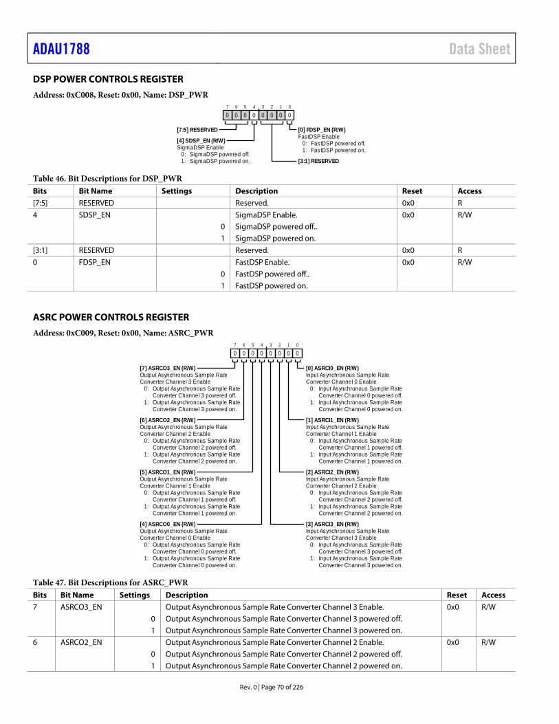
ADAU1788 Data Sheet
Rev. 0 | Page 70 of 226
DSP POWER CONTROLS REGISTER Address: 0xC008, Reset: 0x00, Name: DSP_PWR
FastDSP Enable
1: FastDSP powered on.0: FastDSP powered off.SigmaDSP Enable
1: SigmaDSP powered on.0: SigmaDSP powered off.
0
01
02
03
04
05
06
07
0
[7:5] RESERVED [0] FDSP_EN (R/W)
[4] SDSP_EN (R/W)
[3:1] RESERVED
Table 46. Bit Descriptions for DSP_PWR Bits Bit Name Settings Description Reset Access [7:5] RESERVED Reserved. 0x0 R 4 SDSP_EN SigmaDSP Enable. 0x0 R/W 0 SigmaDSP powered off.. 1 SigmaDSP powered on. [3:1] RESERVED Reserved. 0x0 R 0 FDSP_EN FastDSP Enable. 0x0 R/W 0 FastDSP powered off.. 1 FastDSP powered on.
ASRC POWER CONTROLS REGISTER Address: 0xC009, Reset: 0x00, Name: ASRC_PWR
Output Asynchronous Sample RateConverter Channel 3 Enable
1:Converter Channel 3 powered on.Output Asynchronous Sample Rate
0:Converter Channel 3 powered off.Output Asynchronous Sample Rate
Input Asynchronous Sample RateConverter Channel 0 Enable
1:Converter Channel 0 powered on.Input Asynchronous Sample Rate
0:Converter Channel 0 powered off.Input Asynchronous Sample Rate
Output Asynchronous Sample RateConverter Channel 2 Enable
1:Converter Channel 2 powered on.Output Asynchronous Sample Rate
0:Converter Channel 2 powered off.Output Asynchronous Sample Rate
Input Asynchronous Sample RateConverter Channel 1 Enable
1:Converter Channel 1 powered on.Input Asynchronous Sample Rate
0:Converter Channel 1 powered off.Input Asynchronous Sample Rate
Output Asynchronous Sample RateConverter Channel 1 Enable
1:Converter Channel 1 powered on.Output Asynchronous Sample Rate
0:Converter Channel 1 powered off.Output Asynchronous Sample Rate
Input Asynchronous Sample RateConverter Channel 2 Enable
1:Converter Channel 2 powered on.Input Asynchronous Sample Rate
0:Converter Channel 2 powered off.Input Asynchronous Sample Rate
Output Asynchronous Sample RateConverter Channel 0 Enable
1:Converter Channel 0 powered on.Output Asynchronous Sample Rate
0:Converter Channel 0 powered off.Output Asynchronous Sample Rate
Input Asynchronous Sample RateConverter Channel 3 Enable
1:Converter Channel 3 powered on.Input Asynchronous Sample Rate
0:Converter Channel 3 powered off.Input Asynchronous Sample Rate
0
01
02
03
04
05
06
07
0
[7] ASRCO3_EN (R/W) [0] ASRCI0_EN (R/W)
[6] ASRCO2_EN (R/W) [1] ASRCI1_EN (R/W)
[5] ASRCO1_EN (R/W) [2] ASRCI2_EN (R/W)
[4] ASRCO0_EN (R/W) [3] ASRCI3_EN (R/W)
Table 47. Bit Descriptions for ASRC_PWR Bits Bit Name Settings Description Reset Access 7 ASRCO3_EN Output Asynchronous Sample Rate Converter Channel 3 Enable. 0x0 R/W 0 Output Asynchronous Sample Rate Converter Channel 3 powered off. 1 Output Asynchronous Sample Rate Converter Channel 3 powered on. 6 ASRCO2_EN Output Asynchronous Sample Rate Converter Channel 2 Enable. 0x0 R/W 0 Output Asynchronous Sample Rate Converter Channel 2 powered off. 1 Output Asynchronous Sample Rate Converter Channel 2 powered on.

Data Sheet ADAU1788
Rev. 0 | Page 71 of 226
Bits Bit Name Settings Description Reset Access 5 ASRCO1_EN Output Asynchronous Sample Rate Converter Channel 1 Enable. 0x0 R/W 0 Output Asynchronous Sample Rate Converter Channel 1 powered off. 1 Output Asynchronous Sample Rate Converter Channel 1 powered on. 4 ASRCO0_EN Output Asynchronous Sample Rate Converter Channel 0 Enable. 0x0 R/W 0 Output Asynchronous Sample Rate Converter Channel 0 powered off. 1 Output Asynchronous Sample Rate Converter Channel 0 powered on. 3 ASRCI3_EN Input Asynchronous Sample Rate Converter Channel 3 Enable. 0x0 R/W 0 Input Asynchronous Sample Rate Converter Channel 3 powered off. 1 Input Asynchronous Sample Rate Converter Channel 3 powered on. 2 ASRCI2_EN Input Asynchronous Sample Rate Converter Channel 2 Enable. 0x0 R/W 0 Input Asynchronous Sample Rate Converter Channel 2 powered off. 1 Input Asynchronous Sample Rate Converter Channel 2 powered on. 1 ASRCI1_EN Input Asynchronous Sample Rate Converter Channel 1 Enable. 0x0 R/W 0 Input Asynchronous Sample Rate Converter Channel 1 powered off. 1 Input Asynchronous Sample Rate Converter Channel 1 powered on. 0 ASRCI0_EN Input Asynchronous Sample Rate Converter Channel 0 Enable. 0x0 R/W 0 Input Asynchronous Sample Rate Converter Channel 0 powered off. 1 Input Asynchronous Sample Rate Converter Channel 0 powered on.
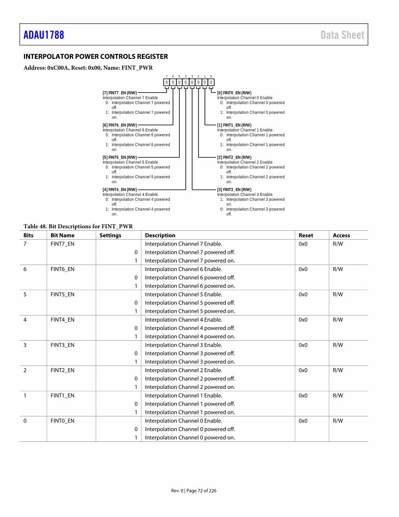
ADAU1788 Data Sheet
Rev. 0 | Page 72 of 226
INTERPOLATOR POWER CONTROLS REGISTER Address: 0xC00A, Reset: 0x00, Name: FINT_PWR
Interpolation Channel 7 Enable
1:on.Interpolation Channel 7 powered
0:off.Interpolation Channel 7 powered
Interpolation Channel 0 Enable
1:on.Interpolation Channel 0 powered
0:off.Interpolation Channel 0 powered
Interpolation Channel 6 Enable
1:on.Interpolation Channel 6 powered
0:off.Interpolation Channel 6 powered
Interpolation Channel 1 Enable
1:on.Interpolation Channel 1 powered
0:off.Interpolation Channel 1 powered
Interpolation Channel 5 Enable
1:on.Interpolation Channel 5 powered
0:off.Interpolation Channel 5 powered
Interpolation Channel 2 Enable
1:on.Interpolation Channel 2 powered
0:off.Interpolation Channel 2 powered
Interpolation Channel 4 Enable
1:on.Interpolation Channel 4 powered
0:off.Interpolation Channel 4 powered
Interpolation Channel 3 Enable
0:off.Interpolation Channel 3 powered
1:on.Interpolation Channel 3 powered
0
01
02
03
04
05
06
07
0
[7] FINT7_EN (R/W) [0] FINT0_EN (R/W)
[6] FINT6_EN (R/W) [1] FINT1_EN (R/W)
[5] FINT5_EN (R/W) [2] FINT2_EN (R/W)
[4] FINT4_EN (R/W) [3] FINT3_EN (R/W)
Table 48. Bit Descriptions for FINT_PWR Bits Bit Name Settings Description Reset Access 7 FINT7_EN Interpolation Channel 7 Enable. 0x0 R/W 0 Interpolation Channel 7 powered off. 1 Interpolation Channel 7 powered on. 6 FINT6_EN Interpolation Channel 6 Enable. 0x0 R/W 0 Interpolation Channel 6 powered off. 1 Interpolation Channel 6 powered on. 5 FINT5_EN Interpolation Channel 5 Enable. 0x0 R/W 0 Interpolation Channel 5 powered off. 1 Interpolation Channel 5 powered on. 4 FINT4_EN Interpolation Channel 4 Enable. 0x0 R/W 0 Interpolation Channel 4 powered off. 1 Interpolation Channel 4 powered on. 3 FINT3_EN Interpolation Channel 3 Enable. 0x0 R/W 0 Interpolation Channel 3 powered off. 1 Interpolation Channel 3 powered on. 2 FINT2_EN Interpolation Channel 2 Enable. 0x0 R/W 0 Interpolation Channel 2 powered off. 1 Interpolation Channel 2 powered on. 1 FINT1_EN Interpolation Channel 1 Enable. 0x0 R/W 0 Interpolation Channel 1 powered off. 1 Interpolation Channel 1 powered on. 0 FINT0_EN Interpolation Channel 0 Enable. 0x0 R/W 0 Interpolation Channel 0 powered off. 1 Interpolation Channel 0 powered on.

Data Sheet ADAU1788
Rev. 0 | Page 73 of 226
DECIMATOR POWER CONTROLS REGISTER Address: 0xC00B, Reset: 0x00, Name: FDEC_PWR
Decimator Channel 7 Enable
1: Decimator Channel 7 powered on.0: Decimator Channel 7 powered off.
Decimator Channel 0 Enable
1: Decimator Channel 0 powered on.0: Decimator Channel 0 powered off.
Decimator Channel 6 Enable
1: Decimator Channel 6 powered on.0: Decimator Channel 6 powered off.
Decimator Channel 1 Enable
1: Decimator Channel 1 powered on.0: Decimator Channel 1 powered off.
Decimator Channel 5 Enable
1: Decimator Channel 5 powered on.0: Decimator Channel 5 powered off.
Decimator Channel 2 Enable
1: Decimator Channel 2 powered on.0: Decimator Channel 2 powered off.
Decimator Channel 4 Enable
1: Decimator Channel 4 powered on.0: Decimator Channel 4 powered off.
Decimator Channel 3 Enable
1: Decimator Channel 3 powered on.0: Decimator Channel 3 powered off.
0
01
02
03
04
05
06
07
0
[7] FDEC7_EN (R/W) [0] FDEC0_EN (R/W)
[6] FDEC6_EN (R/W) [1] FDEC1_EN (R/W)
[5] FDEC5_EN (R/W) [2] FDEC2_EN (R/W)
[4] FDEC4_EN (R/W) [3] FDEC3_EN (R/W)
Table 49. Bit Descriptions for FDEC_PWR Bits Bit Name Settings Description Reset Access 7 FDEC7_EN Decimator Channel 7 Enable. 0x0 R/W 0 Decimator Channel 7 powered off. 1 Decimator Channel 7 powered on. 6 FDEC6_EN Decimator Channel 6 Enable. 0x0 R/W 0 Decimator Channel 6 powered off. 1 Decimator Channel 6 powered on. 5 FDEC5_EN Decimator Channel 5 Enable. 0x0 R/W 0 Decimator Channel 5 powered off. 1 Decimator Channel 5 powered on. 4 FDEC4_EN Decimator Channel 4 Enable. 0x0 R/W 0 Decimator Channel 4 powered off. 1 Decimator Channel 4 powered on. 3 FDEC3_EN Decimator Channel 3 Enable. 0x0 R/W 0 Decimator Channel 3 powered off. 1 Decimator Channel 3 powered on. 2 FDEC2_EN Decimator Channel 2 Enable. 0x0 R/W 0 Decimator Channel 2 powered off. 1 Decimator Channel 2 powered on. 1 FDEC1_EN Decimator Channel 1 Enable. 0x0 R/W 0 Decimator Channel 1 powered off. 1 Decimator Channel 1 powered on. 0 FDEC0_EN Decimator Channel 0 Enable. 0x0 R/W 0 Decimator Channel 0 powered off. 1 Decimator Channel 0 powered on.
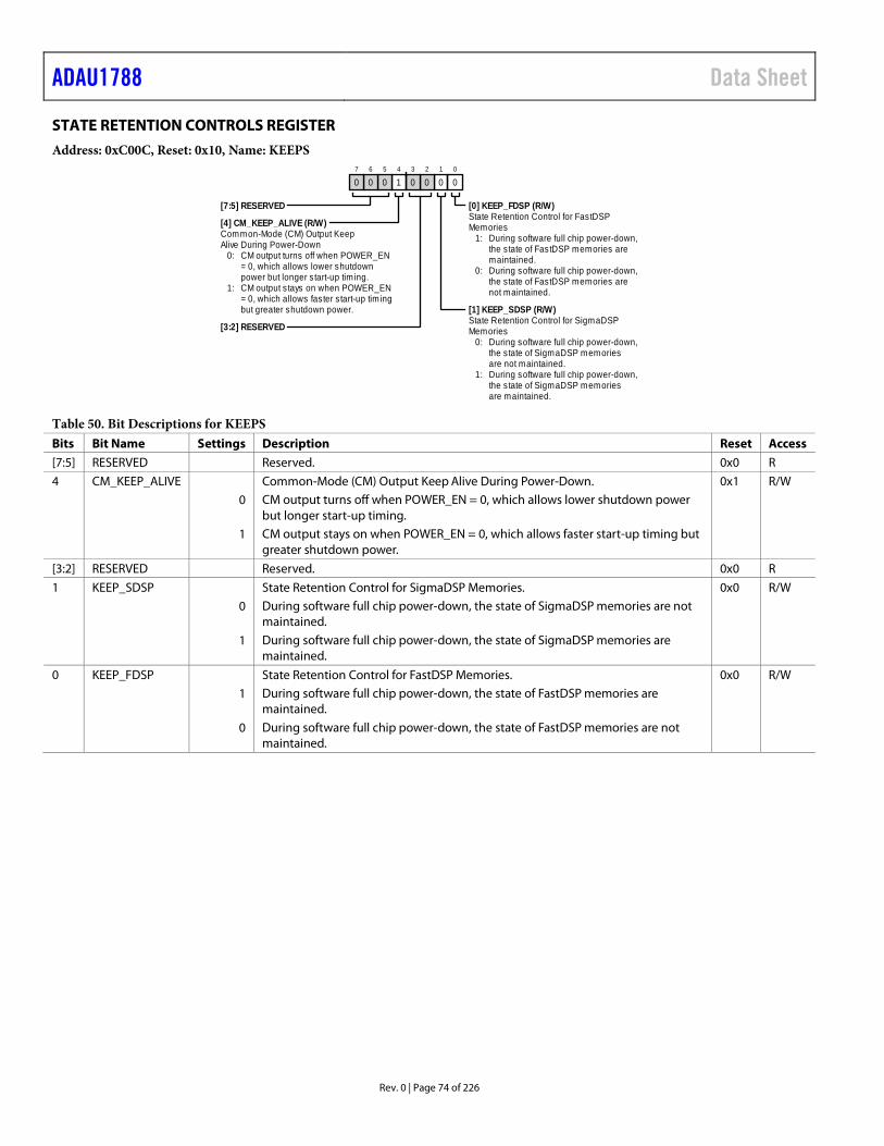
ADAU1788 Data Sheet
Rev. 0 | Page 74 of 226
STATE RETENTION CONTROLS REGISTER Address: 0xC00C, Reset: 0x10, Name: KEEPS
State Retention Control for FastDSPMemories
0:
not maintained.the state of FastDSP memories areDuring software full chip power-down,
1:
maintained.the state of FastDSP memories areDuring software full chip power-down,Common-Mode (CM) Output Keep
Alive During Power-Down
1:
but greater shutdown power.= 0, which allows faster s tart-up tim ingCM output s tays on when POWER_EN
0:
power but longer s tart-up tim ing.= 0, which allows lower shutdownCM output turns off when POWER_EN
State Retention Control for SigmaDSPMemories
1:
are maintained.the state of SigmaDSP memoriesDuring software full chip power-down,
0:
are not maintained.the state of SigmaDSP memoriesDuring software full chip power-down,
0
01
02
03
04
15
06
07
0
[7:5] RESERVED [0] KEEP_FDSP (R/W)
[4] CM_KEEP_ALIVE (R/W)
[1] KEEP_SDSP (R/W)
[3:2] RESERVED
Table 50. Bit Descriptions for KEEPS Bits Bit Name Settings Description Reset Access [7:5] RESERVED Reserved. 0x0 R 4 CM_KEEP_ALIVE Common-Mode (CM) Output Keep Alive During Power-Down. 0x1 R/W 0 CM output turns off when POWER_EN = 0, which allows lower shutdown power
but longer start-up timing.
1 CM output stays on when POWER_EN = 0, which allows faster start-up timing but greater shutdown power.
[3:2] RESERVED Reserved. 0x0 R 1 KEEP_SDSP State Retention Control for SigmaDSP Memories. 0x0 R/W 0 During software full chip power-down, the state of SigmaDSP memories are not
maintained.
1 During software full chip power-down, the state of SigmaDSP memories are maintained.
0 KEEP_FDSP State Retention Control for FastDSP Memories. 0x0 R/W 1 During software full chip power-down, the state of FastDSP memories are
maintained.
0 During software full chip power-down, the state of FastDSP memories are not maintained.

Data Sheet ADAU1788
Rev. 0 | Page 75 of 226
CHIP POWER CONTROL REGISTER Address: 0xC00D, Reset: 0x10, Name: CHIP_PWR
Controls Internal DVDD Power Gating
1:
SDSP.block enabling of PLL, FDSP, andEnables internal DVDD supply. Allows
0: Disables internal DVDD supply.DVDD LDO Regulator Output Voltage
11: Reserved.10: Reserved.01: DVDD regulator is set to 0.9 V.00: Reserved.
Master Block Level Enable. Gatesblock level enabling of all blocksexcept PLL, crystal, FDSP, and SDSP.
1:block enable set are enabled.All blocks that have their respective
0: All blocks are disabled.
Disables High Power CM Start-UpBoost Mode
1: CM pin fast charge is disabled.0: CM pin fast charge is enabled.
0
01
02
03
04
15
06
07
0
[7:6] RESERVED [0] POWER_EN (R/W)
[5:4] DLDO_CTRL (R/W)
[1] MASTER_BLOCK_EN (R/W)
[3] RESERVED
[2] CM_STARTUP_OVER (R/W)
Table 51. Bit Descriptions for CHIP_PWR Bits Bit Name Settings Description Reset Access [7:6] RESERVED Reserved. 0x0 R [5:4] DLDO_CTRL DVDD LDO Regulator Output Voltage. 0x1 R/W 00 Reserved. 01 DVDD regulator is set to 0.9 V. 10 Reserved. 11 Reserved. 3 RESERVED Reserved. 0x0 R 2 CM_STARTUP_OVER Disables High Power CM Start-Up Boost Mode. 0x0 R/W 0 CM pin fast charge is enabled. 1 CM pin fast charge is disabled. 1 MASTER_BLOCK_EN Master Block Level Enable. Gates block level enabling of all blocks except
PLL, crystal, FDSP, and SDSP. 0x0 R/W
0 All blocks are disabled. 1 All blocks that have their respective block enable set are enabled. 0 POWER_EN Controls Internal DVDD Power Gating 0x0 R/W 0 Disables internal DVDD supply. 1 Enables internal DVDD supply. Allows block enabling of PLL, FDSP, and SDSP.

ADAU1788 Data Sheet
Rev. 0 | Page 76 of 226
CLOCK CONTROL REGISTER Address: 0xC00E, Reset: 0xC8, Name: CLK_CTRL1
Source for Phase SynchronizationSignal to Phase Align Multiple Chips.
11:generated.Phase synchronization s ignal internally
10:
is asynchronous to core clock.s ignal. Used when frame clock s ignalInput ASRC used for phase synchronization
0:synchronization.FSYNC_0 s ignal used for phase
PLL Source Clock Selection
10: BCLK_0 pin is PLL source.1: FSYNC_0 pin is PLL source.0: MCLKIN pin or crystal is PLL source.
PLL Bypass Control
1:
setting and must be 24.576 MHz.sourced directly from PLL_SOURCEPLL is bypassed. Main chip clock
0:clock.PLL output is source of main chip
Master Clock/Crystal Oscillator Mode
1: Crystal oscillator used.0: Logic level master clock input used.
Type of PLL (Integer/Fractional).
1: Fractional PLL.0: Integer PLL.
0
01
02
03
14
05
06
17
1
[7:6] SYNC_SOURCE (R/W) [2:0] PLL_SOURCE (R/W)
[5] PLL_BYPASS (R/W)
[3] XTAL_MODE (R/W)
[4] PLL_TYPE (R/W)
Table 52. Bit Descriptions for CLK_CTRL1 Bits Bit Name Settings Description Reset Access [7:6] SYNC_SOURCE Source for Phase Synchronization Signal to Phase Align Multiple Chips. 0x3 R/W 0 FSYNC_0 signal used for phase synchronization. 10 Input ASRC used for phase synchronization signal. Used when frame clock signal is
asynchronous to core clock.
11 Phase synchronization signal internally generated. 5 PLL_BYPASS PLL Bypass Control. 0x0 R/W 0 PLL output is source of main chip clock. 1 PLL is bypassed. Main chip clock sourced directly from PLL_SOURCE setting and
must be 24.576 MHz.
4 PLL_TYPE Type of PLL (Integer/Fractional). 0x0 R/W 0 Integer PLL. 1 Fractional PLL. 3 XTAL_MODE Master Clock/Crystal Oscillator Mode. 0x1 R/W 0 Logic level master clock input used. 1 Crystal oscillator used. [2:0] PLL_SOURCE PLL Source Clock Selection. 0x0 R/W 0 MCLKIN pin or crystal is PLL source. 1 FSYNC_0 pin is PLL source. 10 BCLK_0 pin is PLL source.
PLL INPUT DIVIDER REGISTER Address: 0xC00F, Reset: 0x00, Name: CLK_CTRL2
PLL_INPUT_PRESCALER is theinput divider rate
0
01
02
03
04
05
06
07
0
[7:3] RESERVED [2:0] PLL_INPUT_PRESCALER (R/W)
Table 53. Bit Descriptions for CLK_CTRL2 Bits Bit Name Settings Description Reset Access [7:3] RESERVED Reserved. 0x0 R [2:0] PLL_INPUT_PRESCALER PLL_INPUT_PRESCALER is the input divider rate. 0x0 R/W
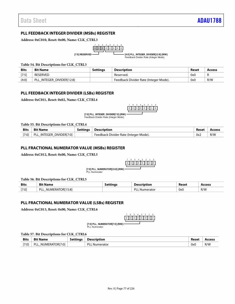
Data Sheet ADAU1788
Rev. 0 | Page 77 of 226
PLL FEEDBACK INTEGER DIVIDER (MSBs) REGISTER Address: 0xC010, Reset: 0x00, Name: CLK_CTRL3
Feedback Divider Rate (Integer Mode).
0
01
02
03
04
05
06
07
0
[7:5] RESERVED [4:0] PLL_INTEGER_DIVIDER[12:8] (R/W)
Table 54. Bit Descriptions for CLK_CTRL3 Bits Bit Name Settings Description Reset Access [7:5] RESERVED Reserved. 0x0 R [4:0] PLL_INTEGER_DIVIDER[12:8] Feedback Divider Rate (Integer Mode). 0x0 R/W
PLL FEEDBACK INTEGER DIVIDER (LSBs) REGISTER Address: 0xC011, Reset: 0x02, Name: CLK_CTRL4
Feedback Divider Rate (Integer Mode).
0
01
12
03
04
05
06
07
0
[7:0] PLL_INTEGER_DIVIDER[7:0] (R/W)
Table 55. Bit Descriptions for CLK_CTRL4 Bits Bit Name Settings Description Reset Access [7:0] PLL_INTEGER_DIVIDER[7:0] Feedback Divider Rate (Integer Mode). 0x2 R/W
PLL FRACTIONAL NUMERATOR VALUE (MSBs) REGISTER Address: 0xC012, Reset: 0x00, Name: CLK_CTRL5
PLL Numerator
0
01
02
03
04
05
06
07
0
[7:0] PLL_NUMERATOR[15:8] (R/W)
Table 56. Bit Descriptions for CLK_CTRL5 Bits Bit Name Settings Description Reset Access [7:0] PLL_NUMERATOR[15:8] PLL Numerator 0x0 R/W
PLL FRACTIONAL NUMERATOR VALUE (LSBs) REGISTER Address: 0xC013, Reset: 0x00, Name: CLK_CTRL6
PLL Numerator
0
01
02
03
04
05
06
07
0
[7:0] PLL_NUMERATOR[7:0] (R/W)
Table 57. Bit Descriptions for CLK_CTRL6 Bits Bit Name Settings Description Reset Access [7:0] PLL_NUMERATOR[7:0] PLL Numerator 0x0 R/W

ADAU1788 Data Sheet
Rev. 0 | Page 78 of 226
PLL FRACTIONAL DENOMINATOR (MSBs) REGISTER Address: 0xC014, Reset: 0x00, Name: CLK_CTRL7
PLL Denominator
0
01
02
03
04
05
06
07
0
[7:0] PLL_DENOMINATOR[15:8] (R/W)
Table 58. Bit Descriptions for CLK_CTRL7 Bits Bit Name Settings Description Reset Access [7:0] PLL_DENOMINATOR[15:8] PLL Denominator 0x0 R/W
PLL FRACTIONAL DENOMINATOR (LSBs) REGISTER Address: 0xC015, Reset: 0x00, Name: CLK_CTRL8
PLL Denominator
0
01
02
03
04
05
06
07
0
[7:0] PLL_DENOMINATOR[7:0] (R/W)
Table 59. Bit Descriptions for CLK_CTRL8 Bits Bit Name Settings Description Reset Access [7:0] PLL_DENOMINATOR[7:0] PLL Denominator 0x0 R/W
PLL UPDATE REGISTER Address: 0xC016, Reset: 0x00, Name: CLK_CTRL9
Update PLL Configuration
1:settings.Write of 1 updates all PLL configuration
0: Write of 0 does nothing.
0
01
02
03
04
05
06
07
0
[7:1] RESERVED [0] PLL_UPDATE (R/W1T)
Table 60. Bit Descriptions for CLK_CTRL9 Bits Bit Name Settings Description Reset Access [7:1] RESERVED Reserved. 0x0 R 0 PLL_UPDATE Update PLL Configuration. 0x0 R/W1T 0 Write of 0 does nothing. 1 Write of 1 updates all PLL configuration settings.

Data Sheet ADAU1788
Rev. 0 | Page 79 of 226
ADC SAMPLE RATE CONTROL REGISTER Address: 0xC017, Reset: 0x22, Name: ADC_CTRL1
ADC Channel 0 and Channel 1 SampleRate Selection
110: 768 kHz sample rate.101: 384 kHz sample rate.100: 192 kHz sample rate.011: 96 kHz sample rate.010: 48 kHz sample rate.001: 24 kHz sample rate.000: 12 kHz sample rate.ADC Channel 0 and Channel 1 Decimation
Filter Order
1:delay.Higher order decimation filter: higher
0:delay.Lower order decimation filter: lower
0
01
12
03
04
05
16
07
0
[7:4] RESERVED [2:0] ADC01_FS (R/W)
[3] ADC01_DEC_ORDER (R/W)
Table 61. Bit Descriptions for ADC_CTRL1 Bits Bit Name Settings Description Reset Access [7:4] RESERVED Reserved. 0x2 R/W 3 ADC01_DEC_ORDER ADC Channel 0 and Channel 1 Decimation Filter Order. 0x0 R/W 0 Lower order decimation filter: lower delay. 1 Higher order decimation filter: higher delay. [2:0] ADC01_FS ADC Channel 0 and Channel 1 Sample Rate Selection. 0x2 R/W 000 12 kHz sample rate. 001 24 kHz sample rate. 010 48 kHz sample rate. 011 96 kHz sample rate. 100 192 kHz sample rate. 101 384 kHz sample rate. 110 768 kHz sample rate.
ADC IBIAS CONTROLS REGISTER Address: 0xC018, Reset: 0x00, Name: ADC_CTRL2
ADC Channel 0 and Channel 1 BiasCurrent Setting
011: Power saving.010: Enhanced performance.001: Extreme power saving.000: Normal operation (default).
0
01
02
03
04
05
06
07
0
[7:3] RESERVED [2:0] ADC01_IBIAS (R/W)
Table 62. Bit Descriptions for ADC_CTRL2 Bits Bit Name Settings Description Reset Access [7:3] RESERVED Reserved. 0x0 R [2:0] ADC01_IBIAS ADC Channel 0 and Channel 1 Bias Current Setting. Higher bias currents result in
higher performance. 0x0 R/W
000 Normal operation (default). 001 Extreme power saving. 010 Enhanced performance. 011 Power saving.

ADAU1788 Data Sheet
Rev. 0 | Page 80 of 226
ADC HIGH-PASS FILTER CONTROL REGISTER Address: 0xC019, Reset: 0x00, Name: ADC_CTRL3
ADC Channel 0 Enable High-PassFilter
1: ADC high-pass filter on.0: ADC high-pass filter off.ADC Channel 1 Enable High-Pass
Filter
1: ADC high-pass filter on.0: ADC high-pass filter off.
0
01
02
03
04
05
06
07
0
[7:2] RESERVED [0] ADC0_HPF_EN (R/W)
[1] ADC1_HPF_EN (R/W)
Table 63. Bit Descriptions for ADC_CTRL3 Bits Bit Name Settings Description Reset Access [7:2] RESERVED Reserved. 0x0 R 1 ADC1_HPF_EN ADC Channel 1 Enable High-Pass Filter. 0x0 R/W 0 ADC high-pass filter off. 1 ADC high-pass filter on. 0 ADC0_HPF_EN ADC Channel 0 Enable High-Pass Filter. 0x0 R/W 0 ADC high-pass filter off. 1 ADC high-pass filter on.
ADC MUTE AND COMPENSATION CONTROL REGISTER Address: 0xC01A, Reset: 0x40, Name: ADC_CTRL4
ADC Channel 0 and Channel 1 FrequencyResponse Compensation
1:(higher delay).High frequency response is compensated
0:(lower delay).High frequency response is not compensatedADC Volume Zero Cross Control
1:crossing.Volume change only occurs at zero
0: Volume change occurs at any time.
ADC Volume Link
1:volume value.All ADC channels use Channel 0
0:volume value.Each ADC channel uses its respective
ADC Hard Volume
1: Hard/immediate volume change.0: Soft volume ramping.
0
01
02
03
04
05
06
17
0
[7] RESERVED [0] ADC01_FCOMP (R/W)
[6] ADC_VOL_ZC (R/W)
[3:1] RESERVED[5] ADC_VOL_LINK (R/W)
[4] ADC_HARD_VOL (R/W)
Table 64. Bit Descriptions for ADC_CTRL4 Bits Bit Name Settings Description Reset Access 7 RESERVED Reserved. 0x0 R 6 ADC_VOL_ZC ADC Volume Zero Cross Control. 0x1 R/W 0 Volume change occurs at any time. 1 Volume change only occurs at zero crossing. 5 ADC_VOL_LINK ADC Volume Link. 0x0 R/W 0 Each ADC channel uses its respective volume value. 1 All ADC channels use Channel 0 volume value. 4 ADC_HARD_VOL ADC Hard Volume. 0x0 R/W 0 Soft volume ramping. 1 Hard/immediate volume change. [3:1] RESERVED Reserved. 0x0 R 0 ADC01_FCOMP ADC Channel 0 and Channel 1 Frequency Response Compensation. 0x0 R/W 0 High frequency response is not compensated (lower delay). 1 High frequency response is compensated (higher delay).

Data Sheet ADAU1788
Rev. 0 | Page 81 of 226
ANALOG INPUT PRECHARGE TIME REGISTER Address: 0xC01B, Reset: 0x26, Name: ADC_CTRL5
Analog Inputs Precharge Time Selection.
0xF: 400 ms precharge.0xE: 300 ms precharge.0xD: 250 ms precharge.
...0x2: 10 ms precharge.0x1: 5 ms precharge.0x0: No precharge.Configures the ADCs for differential
operation
0
01
12
13
04
05
16
07
0
[7:5] RESERVED [3:0] ADC_AIN_CHRG_TIME (R/W)
[4] DIFF_INPUT (R/W)
Table 65. Bit Descriptions for ADC_CTRL5 Bits Bit Name Settings Description Reset Access [7:5] RESERVED Reserved. 0x1 R 4 DIFF_INPUT Configures the ADCs for differential operation. 0x0 R/W [3:0] ADC_AIN_CHRG_TIME Analog Inputs Precharge Time Selection. Controls the amount of time the
precharge circuit is used to charge up the coupling capacitors. The time used depends on the value of the capacitor used and the required start-up time of the ADC.
0x6 R/W
0x0 No Precharge. 0x1 5 ms precharge. 0x2 10 ms precharge. 0x3 20 ms precharge. 0x4 30 ms precharge. 0x5 40 ms precharge. 0x6 50 ms precharge. 0x7 60 ms precharge. 0x8 80 ms precharge. 0x9 100 ms precharge. 0xA 125 ms precharge. 0xB 150 ms precharge. 0xC 200 ms precharge. 0xD 250 ms precharge. 0xE 300 ms precharge. 0xF 400 ms precharge.

ADAU1788 Data Sheet
Rev. 0 | Page 82 of 226
ADC CHANNEL MUTES REGISTER Address: 0xC01C, Reset: 0x00, Name: ADC_MUTES
ADC Channel 0 Mute Control
1: ADC muted.0: ADC unmuted.ADC Channel 1 Mute Control
1: ADC muted.0: ADC unmuted.
0
01
02
03
04
05
06
07
0
[7:2] RESERVED [0] ADC0_MUTE (R/W)
[1] ADC1_MUTE (R/W)
Table 66. Bit Descriptions for ADC_MUTES Bits Bit Name Settings Description Reset Access [7:2] RESERVED Reserved. 0x0 R 1 ADC1_MUTE ADC Channel 1 Mute Control. 0x0 R/W 0 ADC unmuted. 1 ADC muted. 0 ADC0_MUTE ADC Channel 0 Mute Control. 0x0 R/W 0 ADC unmuted. 1 ADC muted.
ADC CHANNEL 0 VOLUME CONTROL REGISTER Address: 0xC01D, Reset: 0x40, Name: ADC0_VOL
ADC Channel 0 Volume Control.
11111111: Mute.11111110: −71.25 dB.11111101: −70.875 dB.
...00000010: +23.35 dB.00000001: +23.625 dB.00000000: +24 dB.
0
01
02
03
04
05
06
17
0
[7:0] ADC0_VOL (R/W)
Table 67. Bit Descriptions for ADC0_VOL Bits Bit Name Settings Description Reset Access [7:0] ADC0_VOL ADC Channel 0 Volume Control. 0x40 R/W 00000000 +24 dB. 00000001 +23.625 dB. 00000010 +23.35 dB. 00000011 +22.875 dB. 00000100 +22.5 dB. … … 00111111 +0.375 dB. 01000000 0 dB. 01000001 −0.375 dB. … … 11111101 −70.875 dB. 11111110 −71.25 dB. 11111111 Mute.

Data Sheet ADAU1788
Rev. 0 | Page 83 of 226
ADC CHANNEL 1 VOLUME CONTROL REGISTER Address: 0xC01E, Reset: 0x40, Name: ADC1_VOL
ADC Channel 1 Volume Control
11111111: Mute.11111110: −71.25 dB.11111101: −70.875 dB.
...00000010: +23.35 dB.00000001: +23.625 dB.00000000: +24 dB.
0
01
02
03
04
05
06
17
0
[7:0] ADC1_VOL (R/W)
Table 68. Bit Descriptions for ADC1_VOL Bits Bit Name Settings Description Reset Access [7:0] ADC1_VOL ADC Channel 1 Volume Control. 0x40 R/W 00000000 +24 dB. 00000001 +23.625 dB. 00000010 +23.35 dB. 00000011 +22.875 dB. 00000100 +22.5 dB. … … 00111111 +0.375 dB. 01000000 0 dB. 01000001 −0.375 dB. … … 11111101 −70.875 dB. 11111110 −71.25 dB. 11111111 Mute.

ADAU1788 Data Sheet
Rev. 0 | Page 84 of 226
PGA CHANNEL 0 GAIN CONTROL MSBs, MUTE, BOOST, AND SLEW REGISTER Address: 0xC021, Reset: 0x00, Name: PGA0_CTRL1
PGA Channel 0 Gain Slew Disable
1: PGA s lew disabled.0: PGA s lew enabled.
PGA Channel 0 Gain Control
10111100000: 35.25 dB.10111000000: 34.5 dB.10110100000: 33.75 dB.
...00001000000: 1.5 dB.00000100000: 0.75 dB.00000000000: 0 dB.
PGA Channel 0 Gain Boost Control
1:in PGA0_GAIN.Additional 10 dB gain above setting
0:in PGA0_GAIN.No additional PGA0 gain above setting
0
01
02
03
04
05
06
07
0
[7] PGA0_SLEW_DIS (R/W) [5:0] PGA0_GAIN[10:5] (R/W)
[6] PGA0_BOOST (R/W)
Table 69. Bit Descriptions for PGA0_CTRL1 Bits Bit Name Settings Description Reset Access 7 PGA0_SLEW_DIS PGA Channel 0 Gain Slew Disable. 0x0 R/W 0 PGA slew enabled. 1 PGA slew disabled. 6 PGA0_BOOST PGA Channel 0 Gain Boost Control. 0x0 R/W 0 No additional PGA0 gain above setting in PGA0_GAIN. 1 Additional 10 dB gain above setting in PGA0_GAIN. [5:0] PGA0_GAIN[10:5] PGA Channel 0 Gain Control. 0x0 R/W 00000000000 0 dB. 00000100000 0.75 dB. 00001000000 1.5 dB. … … 10110100000 33.75 dB. 10111000000 34.5 dB. 10111100000 35.25 dB.
PGA CHANNEL 0 GAIN CONTROL LSBs REGISTER Address: 0xC022, Reset: 0x00, Name: PGA0_CTRL2
PGA Channel 0 Gain Control
10111100000: 35.25 dB.10111000000: 34.5 dB.10110100000: 33.75 dB.
...00001000000: 1.5 dB.00000100000: 0.75 dB.00000000000: 0 dB.
0
01
02
03
04
05
06
07
0
[7:5] RESERVED [4:0] PGA0_GAIN[4:0] (R/W)
Table 70. Bit Descriptions for PGA0_CTRL2 Bits Bit Name Settings Description Reset Access [7:5] RESERVED Reserved. 0x0 R [4:0] PGA0_GAIN[4:0] PGA Channel 0 Gain Control. 0x0 R/W 00000000000 0 dB. 00000100000 0.75 dB. 00001000000 1.5 dB. … … 10110100000 33.75 dB. 10111000000 34.5 dB. 10111100000 35.25 dB.
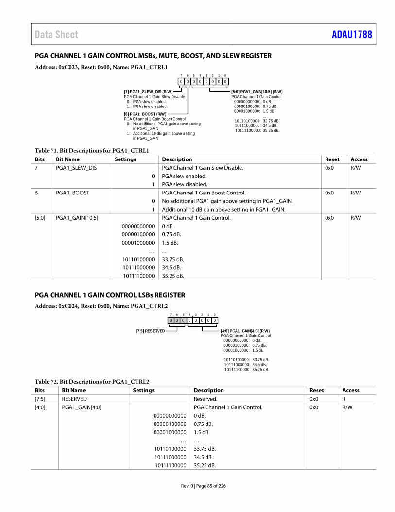
Data Sheet ADAU1788
Rev. 0 | Page 85 of 226
PGA CHANNEL 1 GAIN CONTROL MSBs, MUTE, BOOST, AND SLEW REGISTER Address: 0xC023, Reset: 0x00, Name: PGA1_CTRL1
PGA Channel 1 Gain Slew Disable
1: PGA s lew disabled.0: PGA s lew enabled.
PGA Channel 1 Gain Control
10111100000: 35.25 dB.10111000000: 34.5 dB.10110100000: 33.75 dB.
...00001000000: 1.5 dB.00000100000: 0.75 dB.00000000000: 0 dB.
PGA Channel 1 Gain Boost Control
1:in PGA1_GAIN.Additional 10 dB gain above setting
0:in PGA1_GAIN.No additional PGA1 gain above setting
0
01
02
03
04
05
06
07
0
[7] PGA1_SLEW_DIS (R/W) [5:0] PGA1_GAIN[10:5] (R/W)
[6] PGA1_BOOST (R/W)
Table 71. Bit Descriptions for PGA1_CTRL1 Bits Bit Name Settings Description Reset Access 7 PGA1_SLEW_DIS PGA Channel 1 Gain Slew Disable. 0x0 R/W 0 PGA slew enabled. 1 PGA slew disabled. 6 PGA1_BOOST PGA Channel 1 Gain Boost Control. 0x0 R/W 0 No additional PGA1 gain above setting in PGA1_GAIN. 1 Additional 10 dB gain above setting in PGA1_GAIN. [5:0] PGA1_GAIN[10:5] PGA Channel 1 Gain Control. 0x0 R/W 00000000000 0 dB. 00000100000 0.75 dB. 00001000000 1.5 dB. … … 10110100000 33.75 dB. 10111000000 34.5 dB. 10111100000 35.25 dB.
PGA CHANNEL 1 GAIN CONTROL LSBs REGISTER Address: 0xC024, Reset: 0x00, Name: PGA1_CTRL2
PGA Channel 1 Gain Control
10111100000: 35.25 dB.10111000000: 34.5 dB.10110100000: 33.75 dB.
...00001000000: 1.5 dB.00000100000: 0.75 dB.00000000000: 0 dB.
0
01
02
03
04
05
06
07
0
[7:5] RESERVED [4:0] PGA1_GAIN[4:0] (R/W)
Table 72. Bit Descriptions for PGA1_CTRL2 Bits Bit Name Settings Description Reset Access [7:5] RESERVED Reserved. 0x0 R [4:0] PGA1_GAIN[4:0] PGA Channel 1 Gain Control. 0x0 R/W 00000000000 0 dB. 00000100000 0.75 dB. 00001000000 1.5 dB. … … 10110100000 33.75 dB. 10111000000 34.5 dB. 10111100000 35.25 dB.

ADAU1788 Data Sheet
Rev. 0 | Page 86 of 226
PGA SLEW RATE AND GAIN LINK REGISTER Address: 0xC029, Reset: 0x00, Name: PGA_CTRL
Controls how fast the PGA is s lewedwhen changing gain.
10: 0.5 dB/ms.01: 1.1 dB/ms.00: 2.2 dB/ms.PGA Gain Link.
1:gain value.All PGA channels use Channel 0
0:gain value.Each PGA channel uses its respective
0
01
02
03
04
05
06
07
0
[7:5] RESERVED [1:0] PGA_SLEW_RATE (R/W)
[4] PGA_GAIN_LINK (R/W)
[3:2] RESERVED
Table 73. Bit Descriptions for PGA_CTRL Bits Bit Name Settings Description Reset Access [7:5] RESERVED Reserved. 0x0 R 4 PGA_GAIN_LINK PGA Gain Link. 0x0 R/W 0 Each PGA channel uses its respective gain value. 1 All PGA channels use Channel 0 gain value. [3:2] RESERVED Reserved. 0x0 R [1:0] PGA_SLEW_RATE Controls how fast the PGA is slewed when changing gain. 0x0 R/W 00 2.2 dB/ms. 01 1.1 dB/ms. 10 0.5 dB/ms.
MICROPHONE BIAS LEVEL AND CURRENT REGISTER Address: 0xC02A, Reset: 0x00, Name: MBIAS_CTRL
Level of the MICBIAS0 Output
1: 0.65 × AVDD.0: 0.9 × AVDD.Microphone Input Bias Current Setting
11: Power saving.10: Enhanced performance.01: Extreme power saving.00: Normal operation (default).
Level of the MICBIAS1 Output
1: 0.65 × AVDD.0: 0.9 × AVDD.
0
01
02
03
04
05
06
07
0
[7:6] RESERVED [0] MBIAS0_LEVEL (R/W)
[5:4] MBIAS_IBIAS (R/W)
[1] MBIAS1_LEVEL (R/W)
[3:2] RESERVED
Table 74. Bit Descriptions for MBIAS_CTRL Bits Bit Name Settings Description Reset Access [7:6] RESERVED Reserved. 0x0 R [5:4] MBIAS_IBIAS Microphone Input Bias Current Setting. Higher bias currents result in higher
performance. 0x0 R/W
00 Normal Operation (Default). 01 Extreme power saving. 10 Enhanced performance. 11 Power saving. [3:2] RESERVED Reserved. 0x0 R 1 MBIAS1_LEVEL Level of the MICBIAS1 Output. 0x0 R/W 0 0.9 × AVDD. 1 0.65 × AVDD. 0 MBIAS0_LEVEL Level of the MICBIAS0 Output. 0x0 R/W 0 0.9 × AVDD. 1 0.65 × AVDD.

Data Sheet ADAU1788
Rev. 0 | Page 87 of 226
DMIC CLOCK RATE CONTROL REGISTER Address: 0xC02B, Reset: 0x33, Name: DMIC_CTRL1
Digital Microphone Clock 0 Rate
100: 6144 kHz clock rate.11: 3072 kHz clock rate.10: 1536 kHz clock rate.
1: 768 kHz clock rate.0: 384 kHz clock rate.Digital Microphone Clock 1 Rate
100: 6144 kHz clock rate.11: 3072 kHz clock rate.10: 1536 kHz clock rate.
1: 768 kHz clock rate.0: 384 kHz clock rate.
0
11
12
03
04
15
16
07
0
[7] RESERVED [2:0] DMIC_CLK0_RATE (R/W)
[6:4] DMIC_CLK1_RATE (R/W)
[3] RESERVED
Table 75. Bit Descriptions for DMIC_CTRL1 Bits Bit Name Settings Description Reset Access 7 RESERVED Reserved. 0x0 R [6:4] DMIC_CLK1_RATE Digital Microphone Clock 1 Rate. 0x3 R/W 0 384 kHz clock rate. 1 768 kHz clock rate. 10 1536 kHz clock rate. 11 3072 kHz clock rate. 100 6144 kHz clock rate. 3 RESERVED Reserved. 0x0 R [2:0] DMIC_CLK0_RATE Digital Microphone Clock 0 Rate. 0x3 R/W 0 384 kHz clock rate. 1 768 kHz clock rate. 10 1536 kHz clock rate. 11 3072 kHz clock rate. 100 6144 kHz clock rate.

ADAU1788 Data Sheet
Rev. 0 | Page 88 of 226
DIGITAL MICROPHONE CHANNEL 0 AND CHANNEL 1 RATE, ORDER, MAPPING, AND EDGE CONTROL REGISTER Address: 0xC02C, Reset: 0x01, Name: DMIC_CTRL2
Digital Microphone Channel 0 andChannel 1 Clock Mapping
1:DMIC_CLK1.Digital m icrophone channels use
0:DMIC_CLK0.Digital m icrophone channels use
Digital Microphone Channel 0 andChannel 1 Output Sample Rate
110: 768 kHz sample rate.101: 384 kHz sample rate.100: 192 kHz sample rate.011: 96 kHz sample rate.010: 48 kHz sample rate.001: 24 kHz sample rate.000: 12 kHz sample rate.
Selects clock edge for Channel 0and Channel 1
1: 1 is ris ing edge, and 0 is falling edge.0: 0 is ris ing edge, and 1 is falling edge.
Digital Microphone Channel 0 andChannel 1 High-Pass Filter Enable
1: High-pass filter on.0: High-pass filter off.Digital Microphone Channel 0 and
Channel 1 Frequency ResponseCompensation
1:(higher delay).High frequency response is compensated
0:(lower delay).High frequency response is not compensated Digital Microphone Channel 0 and
Channel 1 Decimation Filter Order
1: Fifth-order decimation filter.0: Fourth-order decimation filter.
0
11
02
03
04
05
06
07
0
[7] DMIC01_MAP (R/W) [2:0] DMIC01_FS (R/W)
[6] DMIC01_EDGE (R/W)
[3] DMIC01_HPF_EN (R/W)
[5] DMIC01_FCOMP (R/W)
[4] DMIC01_DEC_ORDER (R/W)
Table 76. Bit Descriptions for DMIC_CTRL2 Bits Bit Name Settings Description Reset Access 7 DMIC01_MAP Digital Microphone Channel 0 and Channel 1 Clock Mapping. 0x0 R/W 0 Digital microphone channels use DMIC_CLK0. 1 Digital microphone channels use DMIC_CLK1. 6 DMIC01_EDGE Selects clock edge for Channel 0 and Channel 1. 0x0 R/W 0 0 is rising edge, and 1 is falling edge. 1 1 is rising edge, and 0 is falling edge. 5 DMIC01_FCOMP Digital Microphone Channel 0 and Channel 1 Frequency Response
Compensation. 0x0 R/W
0 High frequency response is not compensated (lower delay). 1 High frequency response is compensated (higher delay). 4 DMIC01_DEC_ORDER Digital Microphone Channel 0 and Channel 1 Decimation Filter Order. 0x0 R/W 0 Fourth-order decimation filter. 1 Fifth-order decimation filter. 3 DMIC01_HPF_EN Digital Microphone Channel 0 and Channel 1 High-Pass Filter Enable. 0x0 R/W 0 High-pass filter off. 1 High-pass filter on. [2:0] DMIC01_FS Digital Microphone Channel 0 and Channel 1 Output Sample Rate. 0x1 R/W 000 12 kHz sample rate. 001 24 kHz sample rate. 010 48 kHz sample rate. 011 96 kHz sample rate. 100 192 kHz sample rate. 101 384 kHz sample rate. 110 768 kHz sample rate.

Data Sheet ADAU1788
Rev. 0 | Page 89 of 226
DIGITAL MICROPHONE CHANNEL 2 AND CHANNEL 3 RATE, ORDER, MAPPING, AND EDGE CONTROL REGISTER Address: 0xC02D, Reset: 0x01, Name: DMIC_CTRL3
Digital Microphone Channel 2 andChannel 3 Clock Mapping
1:DMIC_CLK1.Digital m icrophone channels use
0:DMIC_CLK0.Digital m icrophone channels use
Digital Microphone Channel 2 andChannel 3 Output Sample Rate
110: 768 kHz sample rate.101: 384 kHz sample rate.100: 192 kHz sample rate.011: 96 kHz sample rate.010: 48 kHz sample rate.001: 24 kHz sample rate.000: 12 kHz sample rate.
Selects clock edge for Channel 2and Channel 3
1: 1 is ris ing edge, and 0 is falling edge.0: 0 is ris ing edge, and 1 is falling edge.
Digital Microphone Channel 2 andChannel 3 High-Pass Filter Enable
1: High-pass filter on.0: High-pass filter off.Digital Microphone Channel 2 and
Channel 3 Frequency ResponseCompensation
1:(higher delay).High frequency response is compensated
0:(lower delay).High frequency response is not compensated Digital Microphone Channel 2 and
Channel 3 Decimation Filter Order
1: Fifth-order decimation filter.0: Fourth-order decimation filter.
0
11
02
03
04
05
06
07
0
[7] DMIC23_MAP (R/W) [2:0] DMIC23_FS (R/W)
[6] DMIC23_EDGE (R/W)
[3] DMIC23_HPF_EN (R/W)
[5] DMIC23_FCOMP (R/W)
[4] DMIC23_DEC_ORDER (R/W)
Table 77. Bit Descriptions for DMIC_CTRL3 Bits Bit Name Settings Description Reset Access 7 DMIC23_MAP Digital Microphone Channel 2 and Channel 3 Clock Mapping. 0x0 R/W 0 Digital microphone channels use DMIC_CLK0. 1 Digital microphone channels use DMIC_CLK1. 6 DMIC23_EDGE Selects clock edge for Channel 2 and Channel 3. 0x0 R/W 0 0 is rising edge, and 1 is falling edge. 1 1 is rising edge, and 0 is falling edge. 5 DMIC23_FCOMP Digital Microphone Channel 2 and Channel 3 Frequency Response
Compensation. 0x0 R/W
0 High frequency response is not compensated (lower delay). 1 High frequency response is compensated (higher delay). 4 DMIC23_DEC_ORDER Digital Microphone Channel 2 and Channel 3 Decimation Filter Order. 0x0 R/W 0 Fourth-order decimation filter. 1 Fifth-order decimation filter. 3 DMIC23_HPF_EN Digital Microphone Channel 2 and Channel 3 High-Pass Filter Enable. 0x0 R/W 0 High-pass filter off. 1 High-pass filter on. [2:0] DMIC23_FS Digital Microphone Channel 2 and Channel 3 Output Sample Rate. 0x1 R/W 000 12 kHz sample rate. 001 24 kHz sample rate. 010 48 kHz sample rate. 011 96 kHz sample rate. 100 192 kHz sample rate. 101 384 kHz sample rate. 110 768 kHz sample rate.

ADAU1788 Data Sheet
Rev. 0 | Page 90 of 226
DMIC VOLUME OPTIONS REGISTER Address: 0xC030, Reset: 0x04, Name: DMIC_CTRL6
Digital Microphone Hard Volume
1: Hard/immediate volume change.0: Soft volume ramping.Digital Microphone Volume Zero Cross
Control
1:crossing.Volume change only occurs at zero
0: Volume change occurs at any time.Digital Microphone Volume Link
1:Channel 0 volume value.All digital m icrophone channels use
0:uses its respective volume value.Each digital m icrophone channel
0
01
02
13
04
05
06
07
0
[7:3] RESERVED [0] DMIC_HARD_VOL (R/W)
[2] DMIC_VOL_ZC (R/W)
[1] DMIC_VOL_LINK (R/W)
Table 78. Bit Descriptions for DMIC_CTRL6 Bits Bit Name Settings Description Reset Access [7:3] RESERVED Reserved. 0x0 R 2 DMIC_VOL_ZC Digital Microphone Volume Zero Cross Control. 0x1 R/W 0 Volume change occurs at any time. 1 Volume change only occurs at zero crossing. 1 DMIC_VOL_LINK Digital Microphone Volume Link. 0x0 R/W 0 Each digital microphone channel uses its respective volume value. 1 All digital microphone channels use Channel 0 volume value. 0 DMIC_HARD_VOL Digital Microphone Hard Volume. 0x0 R/W 0 Soft volume ramping. 1 Hard/immediate volume change.
DIGITAL MICROPHONE CHANNEL MUTE CONTROLS REGISTER Address: 0xC031, Reset: 0x00, Name: DMIC_MUTES
Digital Microphone Channel 0 MuteControl
1: Digital m icrophone muted.0: Digital m icrophone unmuted.Digital Microphone Channel 3 Mute
Control
1: Digital m icrophone muted.0: Digital m icrophone unmuted.
Digital Microphone Channel 1 MuteControl
1: Digital m icrophone muted.0: Digital m icrophone unmuted.Digital Microphone Channel 2 Mute
Control
1: Digital m icrophone muted.0: Digital m icrophone unmuted.
0
01
02
03
04
05
06
07
0
[7:4] RESERVED [0] DMIC0_MUTE (R/W)
[3] DMIC3_MUTE (R/W)
[1] DMIC1_MUTE (R/W)
[2] DMIC2_MUTE (R/W)
Table 79. Bit Descriptions for DMIC_MUTES Bits Bit Name Settings Description Reset Access [7:4] RESERVED Reserved. 0x0 R/W 3 DMIC3_MUTE Digital Microphone Channel 3 Mute Control. 0x0 R/W 0 Digital microphone unmuted. 1 Digital microphone muted. 2 DMIC2_MUTE Digital Microphone Channel 2 Mute Control. 0x0 R/W 0 Digital microphone unmuted. 1 Digital microphone muted.

Data Sheet ADAU1788
Rev. 0 | Page 91 of 226
Bits Bit Name Settings Description Reset Access 1 DMIC1_MUTE Digital Microphone Channel 1 Mute Control. 0x0 R/W 0 Digital microphone unmuted. 1 Digital microphone muted. 0 DMIC0_MUTE Digital Microphone Channel 0 Mute Control. 0x0 R/W 0 Digital microphone unmuted. 1 Digital microphone muted.
DIGITAL MICROPHONE CHANNEL 0 VOLUME CONTROL REGISTER Address: 0xC032, Reset: 0x40, Name: DMIC_VOL0
Digital Microphone Channel 0 VolumeControl
11111111: Mute.11111110: −71.25 dB.11111101: −70.875 dB.
...00000010: +23.35 dB.00000001: +23.625 dB.00000000: +24 dB.
0
01
02
03
04
05
06
17
0
[7:0] DMIC0_VOL (R/W)
Table 80. Bit Descriptions for DMIC_VOL0 Bits Bit Name Settings Description Reset Access [7:0] DMIC0_VOL Digital Microphone Channel 0 Volume Control. 0x40 R/W 00000000 +24 dB. 00000001 +23.625 dB. 00000010 +23.35 dB. 00000011 +22.875 dB. 00000100 +22.5 dB. … … 00111111 +0.375 dB. 01000000 0 dB. 01000001 −0.375 dB. … … 11111101 −70.875 dB. 11111110 −71.25 dB. 11111111 Mute.

ADAU1788 Data Sheet
Rev. 0 | Page 92 of 226
DIGITAL MICROPHONE CHANNEL 1 VOLUME CONTROL REGISTER Address: 0xC033, Reset: 0x40, Name: DMIC_VOL1
Digital Microphone Channel 1 VolumeControl
11111111: Mute.11111110: −71.25 dB.11111101: −70.875 dB.
...00000010: +23.35 dB.00000001: +23.625 dB.00000000: +24 dB.
0
01
02
03
04
05
06
17
0
[7:0] DMIC1_VOL (R/W)
Table 81. Bit Descriptions for DMIC_VOL1 Bits Bit Name Settings Description Reset Access [7:0] DMIC1_VOL Digital Microphone Channel 1 Volume Control. 0x40 R/W 00000000 +24 dB. 00000001 +23.625 dB. 00000010 +23.35 dB. 00000011 +22.875 dB. 00000100 +22.5 dB. … … 00111111 +0.375 dB. 01000000 0 dB. 01000001 −0.375 dB. … … 11111101 −70.875 dB. 11111110 −71.25 dB. 11111111 Mute.

Data Sheet ADAU1788
Rev. 0 | Page 93 of 226
DIGITAL MICROPHONE CHANNEL 2 VOLUME CONTROL REGISTER Address: 0xC034, Reset: 0x40, Name: DMIC_VOL2
Digital Microphone Channel 2 VolumeControl
11111111: Mute.11111110: −71.25 dB.11111101: −70.875 dB.
...00000010: +23.35 dB.00000001: +23.625 dB.00000000: +24 dB.
0
01
02
03
04
05
06
17
0
[7:0] DMIC2_VOL (R/W)
Table 82. Bit Descriptions for DMIC_VOL2 Bits Bit Name Settings Description Reset Access [7:0] DMIC2_VOL Digital Microphone Channel 2 Volume Control. 0x40 R/W 00000000 +24 dB. 00000001 +23.625 dB. 00000010 +23.35 dB. 00000011 +22.875 dB. 00000100 +22.5 dB. … … 00111111 +0.375 dB. 01000000 0 dB. 01000001 −0.375 dB. … … 11111101 −70.875 dB. 11111110 −71.25 dB. 11111111 Mute.

ADAU1788 Data Sheet
Rev. 0 | Page 94 of 226
DIGITAL MICROPHONE CHANNEL 3 VOLUME CONTROL REGISTER Address: 0xC035, Reset: 0x40, Name: DMIC_VOL3
Digital Microphone Channel 3 VolumeControl
11111111: Mute.11111110: −71.25 dB.11111101: −70.875 dB.
...00000010: +23.35 dB.00000001: +23.625 dB.00000000: +24 dB.
0
01
02
03
04
05
06
17
0
[7:0] DMIC3_VOL (R/W)
Table 83. Bit Descriptions for DMIC_VOL3 Bits Bit Name Settings Description Reset Access [7:0] DMIC3_VOL Digital Microphone Channel 3 Volume Control. 0x40 R/W 00000000 +24 dB. 00000001 +23.625 dB. 00000010 +23.35 dB. 00000011 +22.875 dB. 00000100 +22.5 dB. … … 00111111 +0.375 dB. 01000000 0 dB. 01000001 −0.375 dB. … … 11111101 −70.875 dB. 11111110 −71.25 dB. 11111111 Mute.
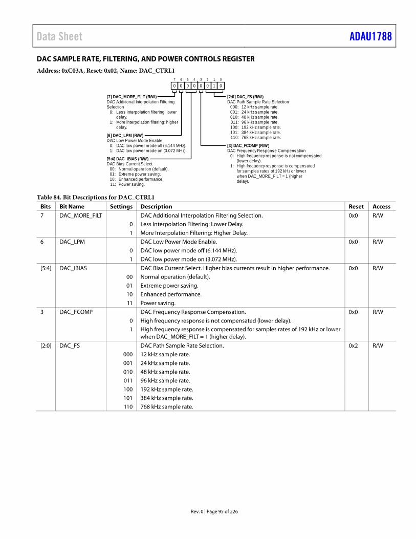
Data Sheet ADAU1788
Rev. 0 | Page 95 of 226
DAC SAMPLE RATE, FILTERING, AND POWER CONTROLS REGISTER Address: 0xC03A, Reset: 0x02, Name: DAC_CTRL1
DAC Additional Interpolation FilteringSelection
1:delay.More interpolation filtering: higher
0:delay.Less interpolation filtering: lower
DAC Path Sample Rate Selection
110: 768 kHz sample rate.101: 384 kHz sample rate.100: 192 kHz sample rate.011: 96 kHz sample rate.010: 48 kHz sample rate.001: 24 kHz sample rate.000: 12 kHz sample rate.
DAC Low Power Mode Enable
1: DAC low power mode on (3.072 MHz).0: DAC low power mode off (6.144 MHz).
DAC Frequency Response Compensation
1:
delay).when DAC_MORE_FILT = 1 (higherfor samples rates of 192 kHz or lowerHigh frequency response is compensated
0:(lower delay).High frequency response is not compensated
DAC Bias Current Select
11: Power saving.10: Enhanced performance.01: Extreme power saving.00: Normal operation (default).
0
01
12
03
04
05
06
07
0
[7] DAC_MORE_FILT (R/W) [2:0] DAC_FS (R/W)
[6] DAC_LPM (R/W)
[3] DAC_FCOMP (R/W)
[5:4] DAC_IBIAS (R/W)
Table 84. Bit Descriptions for DAC_CTRL1 Bits Bit Name Settings Description Reset Access 7 DAC_MORE_FILT DAC Additional Interpolation Filtering Selection. 0x0 R/W 0 Less Interpolation Filtering: Lower Delay. 1 More Interpolation Filtering: Higher Delay. 6 DAC_LPM DAC Low Power Mode Enable. 0x0 R/W 0 DAC low power mode off (6.144 MHz). 1 DAC low power mode on (3.072 MHz). [5:4] DAC_IBIAS DAC Bias Current Select. Higher bias currents result in higher performance. 0x0 R/W 00 Normal operation (default). 01 Extreme power saving. 10 Enhanced performance. 11 Power saving. 3 DAC_FCOMP DAC Frequency Response Compensation. 0x0 R/W 0 High frequency response is not compensated (lower delay). 1 High frequency response is compensated for samples rates of 192 kHz or lower
when DAC_MORE_FILT = 1 (higher delay).
[2:0] DAC_FS DAC Path Sample Rate Selection. 0x2 R/W 000 12 kHz sample rate. 001 24 kHz sample rate. 010 48 kHz sample rate. 011 96 kHz sample rate. 100 192 kHz sample rate. 101 384 kHz sample rate. 110 768 kHz sample rate.

ADAU1788 Data Sheet
Rev. 0 | Page 96 of 226
DAC VOLUME LUNK, HIGH-PASS FILTER, AND MUTE CONTROLS REGISTER Address: 0xC03B, Reset: 0xC4, Name: DAC_CTRL2
DAC Channel 0 Mute Control
1: DAC muted.0: DAC unmuted.
DAC Hard Volume
1: Hard/immediate volume change.0: Soft volume ramping.
DAC Volume Zero Cross Control
1:crossing.Volume change only occurs at zero
0: Volume change occurs at any time.DAC Channel 0 Enable High-PassFilter
1: DAC high-pass filter on.0: DAC high-pass filter off.
DAC Low Power Mode 2 Enable
1:output activity.DAC Low Power Mode 2 on. Reduced
0: DAC Low Power Mode 2 off.
0
01
02
13
04
05
06
17
1
[7] RESERVED [0] RESERVED
[6] DAC0_MUTE (R/W) [1] DAC_HARD_VOL (R/W)
[5] RESERVED [2] DAC_VOL_ZC (R/W)
[4] DAC0_HPF_EN (R/W)
[3] DAC_LPM_II (R/W)
Table 85. Bit Descriptions for DAC_CTRL2 Bits Bit Name Settings Description Reset Access 7 RESERVED Reserved. 0x1 R/W 6 DAC0_MUTE DAC Channel 0 Mute Control. 0x1 R/W 0 DAC unmuted. 1 DAC muted. 5 RESERVED Reserved. 0x0 R/W 4 DAC0_HPF_EN DAC Channel 0 Enable High-Pass Filter. 0x0 R/W 0 DAC high-pass filter off. 1 DAC high-pass filter on. 3 DAC_LPM_II DAC Low Power Mode 2 Enable. 0x0 R/W 0 DAC Low Power Mode 2 off. 1 DAC Low Power Mode 2 on. Reduced output activity. 2 DAC_VOL_ZC DAC Volume Zero Cross Control. 0x1 R/W 0 Volume change occurs at any time. 1 Volume change only occurs at zero crossing. 1 DAC_HARD_VOL DAC Hard Volume. 0x0 R/W 0 Soft volume ramping. 1 Hard/immediate volume change. 0 RESERVED Reserved. 0x0 R/W

Data Sheet ADAU1788
Rev. 0 | Page 97 of 226
DAC CHANNEL 0 VOLUME REGISTER Address: 0xC03C, Reset: 0x40, Name: DAC_VOL0
DAC Channel 0 Volume Control
11111111: Mute.11111110: −71.25 dB.11111101: −70.875 dB.
...00000010: +23.35 dB.00000001: +23.625 dB.00000000: +24 dB.
0
01
02
03
04
05
06
17
0
[7:0] DAC0_VOL (R/W)
Table 86. Bit Descriptions for DAC_VOL0 Bits Bit Name Settings Description Reset Access [7:0] DAC0_VOL DAC Channel 0 Volume Control. 0x40 R/W 00000000 +24 dB. 00000001 +23.625 dB. 00000010 +23.35 dB. 00000011 +22.875 dB. 00000100 +22.5 dB. … … 00111111 +0.375 dB. 01000000 0 dB. 01000001 −0.375 dB. … … 11111101 −70.875 dB. 11111110 −71.25 dB. 11111111 Mute.

ADAU1788 Data Sheet
Rev. 0 | Page 98 of 226
DAC CHANNEL 0 ROUTING REGISTER Address: 0xC03E, Reset: 0x00, Name: DAC_ROUTE0
DAC Channel 0 Input Routing
1001011: Digital Microphone Channel 3.1001010: Digital Microphone Channel 2.1001001: Digital Microphone Channel 1.
...0000010: Serial Port 0 Channel 2.0000001: Serial Port 0 Channel 1.0000000: Serial Port 0 Channel 0.
0
01
02
03
04
05
06
07
0
[7] RESERVED [6:0] DAC0_ROUTE (R/W)
Table 87. Bit Descriptions for DAC_ROUTE0 Bits Bit Name Settings Description Reset Access 7 RESERVED Reserved. 0x0 R [6:0] DAC0_ROUTE DAC Channel 0 Input Routing. 0x0 R/W 0000000 Serial Port 0 Channel 0. 0000001 Serial Port 0 Channel 1. 0000010 Serial Port 0 Channel 2. 0000011 Serial Port 0 Channel 3. 0000100 Serial Port 0 Channel 4. 0000101 Serial Port 0 Channel 5. 0000110 Serial Port 0 Channel 6. 0000111 Serial Port 0 Channel 7. 0001000 Serial Port 0 Channel 8. 0001001 Serial Port 0 Channel 9. 0001010 Serial Port 0 Channel 10. 0001011 Serial Port 0 Channel 11. 0001100 Serial Port 0 Channel 12. 0001101 Serial Port 0 Channel 13. 0001110 Serial Port 0 Channel 14. 0001111 Serial Port 0 Channel 15. 0100000 FastDSP Channel 0. 0100001 FastDSP Channel 1. 0100010 FastDSP Channel 2. 0100011 FastDSP Channel 3. 0100100 FastDSP Channel 4. 0100101 FastDSP Channel 5. 0100110 FastDSP Channel 6. 0100111 FastDSP Channel 7. 0101000 FastDSP Channel 8. 0101001 FastDSP Channel 9. 0101010 FastDSP Channel 10. 0101011 FastDSP Channel 11. 0101100 FastDSP Channel 12. 0101101 FastDSP Channel 13. 0101110 FastDSP Channel 14. 0101111 FastDSP Channel 15. 0110000 SigmaDSP Channel 0. 0110001 SigmaDSP Channel 1. 0110010 SigmaDSP Channel 2. 0110011 SigmaDSP Channel 3. 0110100 SigmaDSP Channel 4.

Data Sheet ADAU1788
Rev. 0 | Page 99 of 226
Bits Bit Name Settings Description Reset Access 0110101 SigmaDSP Channel 5. 0110110 SigmaDSP Channel 6. 0110111 SigmaDSP Channel 7. 0111000 SigmaDSP Channel 8. 0111001 SigmaDSP Channel 9. 0111010 SigmaDSP Channel 10. 0111011 SigmaDSP Channel 11. 0111100 SigmaDSP Channel 12. 0111101 SigmaDSP Channel 13. 0111110 SigmaDSP Channel 14. 0111111 SigmaDSP Channel 15. 1000000 Input ASRC Channel 0. 1000001 Input ASRC Channel 1. 1000010 Input ASRC Channel 2. 1000011 Input ASRC Channel 3. 1000100 ADC Channel 0. 1000101 ADC Channel 1. 1001000 Digital Microphone Channel 0. 1001001 Digital Microphone Channel 1. 1001010 Digital Microphone Channel 2. 1001011 Digital Microphone Channel 3.
HEADPHONE CONTROL REGISTER Address: 0xC040, Reset: 0x00, Name: HP_CTRL
Headphone Channel 0 Output Mode
1:mode.HPOUTP0/HPOUTN0 in headphone
0:mode.HPOUTP0/HPOUTN0 in line output
0
01
02
03
04
05
06
07
0
[7:1] RESERVED [0] HP0_MODE (R/W)
Table 88. Bit Descriptions for HP_CTRL Bits Bit Name Settings Description Reset Access [7:1] RESERVED Reserved. 0x0 R 0 HP0_MODE Headphone Channel 0 Output Mode. 0x0 R/W 0 HPOUTP0/HPOUTN0 in line output mode. 1 HPOUTP0/HPOUTN0 in headphone mode.

ADAU1788 Data Sheet
Rev. 0 | Page 100 of 226
FAST TO SLOW DECIMATOR SAMPLE RATES CHANNEL 0 AND CHANNEL 1 REGISTER Address: 0xC041, Reset: 0x25, Name: FDEC_CTRL1
Decimator Channel 0/Channel 1Input Sampling Rate
110: 768 kHz sample rate.101: 384 kHz sample rate.100: 192 kHz sample rate.011: 96 kHz sample rate.010: 48 kHz sample rate.001: 24 kHz sample rate.Decimator Channel 0/Channel 1
Output Sampling Rate
101: 384 kHz sample rate.100: 192 kHz sample rate.011: 96 kHz sample rate.010: 48 kHz sample rate.001: 24 kHz sample rate.000: 12 kHz sample rate.
0
11
02
13
04
05
16
07
0
[7] RESERVED [2:0] FDEC01_IN_FS (R/W)
[6:4] FDEC01_OUT_FS (R/W)
[3] RESERVED
Table 89. Bit Descriptions for FDEC_CTRL1 Bits Bit Name Settings Description Reset Access 7 RESERVED Reserved. 0x0 R [6:4] FDEC01_OUT_FS Decimator Channel 0/Channel 1 Output Sampling Rate. 0x2 R/W 000 12 kHz sample rate. 001 24 kHz sample rate. 010 48 kHz sample rate. 011 96 kHz sample rate. 100 192 kHz sample rate. 101 384 kHz sample rate. 3 RESERVED Reserved. 0x0 R [2:0] FDEC01_IN_FS Decimator Channel 0/Channel 1 Input Sampling Rate. 0x5 R/W 001 24 kHz sample rate. 010 48 kHz sample rate. 011 96 kHz sample rate. 100 192 kHz sample rate. 101 384 kHz sample rate. 110 768 kHz sample rate.

Data Sheet ADAU1788
Rev. 0 | Page 101 of 226
FAST TO SLOW DECIMATOR SAMPLE RATES CHANNEL 2 AND CHANNEL 3 REGISTER Address: 0xC042, Reset: 0x25, Name: FDEC_CTRL2
Decimator Channel 2/Channel 3Input Sampling Rate
110: 768 kHz sample rate.101: 384 kHz sample rate.100: 192 kHz sample rate.011: 96 kHz sample rate.010: 48 kHz sample rate.001: 24 kHz sample rate.Decimator Channel 2/Channel 3
Output Sampling Rate
101: 384 kHz sample rate.100: 192 kHz sample rate.011: 96 kHz sample rate.010: 48 kHz sample rate.001: 24 kHz sample rate.000: 12 kHz sample rate.
0
11
02
13
04
05
16
07
0
[7] RESERVED [2:0] FDEC23_IN_FS (R/W)
[6:4] FDEC23_OUT_FS (R/W)
[3] RESERVED
Table 90. Bit Descriptions for FDEC_CTRL2 Bits Bit Name Settings Description Reset Access 7 RESERVED Reserved. 0x0 R [6:4] FDEC23_OUT_FS Decimator Channel 2/Channel 3 Output Sampling Rate. 0x2 R/W 000 12 kHz sample rate. 001 24 kHz sample rate. 010 48 kHz sample rate. 011 96 kHz sample rate. 100 192 kHz sample rate. 101 384 kHz sample rate. 3 RESERVED Reserved. 0x0 R [2:0] FDEC23_IN_FS Decimator Channel 2/Channel 3 Input Sampling Rate. 0x5 R/W 001 24 kHz sample rate. 010 48 kHz sample rate. 011 96 kHz sample rate. 100 192 kHz sample rate. 101 384 kHz sample rate. 110 768 kHz sample rate.
FAST TO SLOW DECIMATOR SAMPLE RATES CHANNEL 4 AND CHANNEL 5 REGISTER Address: 0xC043, Reset: 0x25, Name: FDEC_CTRL3
Decimator Channel 4/Channel 5Input Sampling Rate
110: 768 kHz sample rate.101: 384 kHz sample rate.100: 192 kHz sample rate.011: 96 kHz sample rate.010: 48 kHz sample rate.001: 24 kHz sample rate.Decimator Channel 4/Channel 5
Output Sampling Rate
101: 384 kHz sample rate.100: 192 kHz sample rate.011: 96 kHz sample rate.010: 48 kHz sample rate.001: 24 kHz sample rate.000: 12 kHz sample rate.
0
11
02
13
04
05
16
07
0
[7] RESERVED [2:0] FDEC45_IN_FS (R/W)
[6:4] FDEC45_OUT_FS (R/W)
[3] RESERVED
Table 91. Bit Descriptions for FDEC_CTRL3 Bits Bit Name Settings Description Reset Access 7 RESERVED Reserved. 0x0 R [6:4] FDEC45_OUT_FS Decimator Channel 4/Channel 5 Output Sampling Rate. 0x2 R/W 000 12 kHz sample rate. 001 24 kHz sample rate. 010 48 kHz sample rate. 011 96 kHz sample rate. 100 192 kHz sample rate. 101 384 kHz sample rate.

ADAU1788 Data Sheet
Rev. 0 | Page 102 of 226
Bits Bit Name Settings Description Reset Access 3 RESERVED Reserved. 0x0 R [2:0] FDEC45_IN_FS Decimator Channel 4/Channel 5 Input Sampling Rate. 0x5 R/W 001 24 kHz sample rate. 010 48 kHz sample rate. 011 96 kHz sample rate. 100 192 kHz sample rate. 101 384 kHz sample rate. 110 768 kHz sample rate.
FAST TO SLOW DECIMATOR SAMPLE RATES CHANNEL 6 AND CHANNEL 7 REGISTER Address: 0xC044, Reset: 0x25, Name: FDEC_CTRL4
Decimator Channel 6/Channel 7Input Sampling Rate
110: 768 kHz sample rate.101: 384 kHz sample rate.100: 192 kHz sample rate.011: 96 kHz sample rate.010: 48 kHz sample rate.001: 24 kHz sample rate.Decimator Channel 6/Channel 7
Output Sampling Rate
101: 384 kHz sample rate.100: 192 kHz sample rate.011: 96 kHz sample rate.010: 48 kHz sample rate.001: 24 kHz sample rate.000: 12 kHz sample rate.
0
11
02
13
04
05
16
07
0
[7] RESERVED [2:0] FDEC67_IN_FS (R/W)
[6:4] FDEC67_OUT_FS (R/W)
[3] RESERVED
Table 92. Bit Descriptions for FDEC_CTRL4 Bits Bit Name Settings Description Reset Access 7 RESERVED Reserved. 0x0 R [6:4] FDEC67_OUT_FS Decimator Channel 6/Channel 7 Output Sampling Rate. 0x2 R/W 000 12 kHz sample rate. 001 24 kHz sample rate. 010 48 kHz sample rate. 011 96 kHz sample rate. 100 192 kHz sample rate. 101 384 kHz sample rate. 3 RESERVED Reserved. 0x0 R [2:0] FDEC67_IN_FS Decimator Channel 6/Channel 7 Input Sampling Rate. 0x5 R/W 001 24 kHz sample rate. 010 48 kHz sample rate. 011 96 kHz sample rate. 100 192 kHz sample rate. 101 384 kHz sample rate. 110 768 kHz sample rate.

Data Sheet ADAU1788
Rev. 0 | Page 103 of 226
FAST TO SLOW DECIMATOR CHANNEL 0 INPUT ROUTING REGISTER Address: 0xC045, Reset: 0x00, Name: FDEC_ROUTE0
Fast to Slow Decimator Channel0 Input Routing
101011: Digital Microphone Channel 3.101010: Digital Microphone Channel 2.101001: Digital Microphone Channel 1.
...000010: FastDSP Channel 2.000001: FastDSP Channel 1.000000: FastDSP Channel 0.
0
01
02
03
04
05
06
07
0
[7:6] RESERVED [5:0] FDEC0_ROUTE (R/W)
Table 93. Bit Descriptions for FDEC_ROUTE0 Bits Bit Name Settings Description Reset Access [7:6] RESERVED Reserved. 0x0 R [5:0] FDEC0_ROUTE Fast to Slow Decimator Channel 0 Input Routing. 0x0 R/W 000000 FastDSP Channel 0. 000001 FastDSP Channel 1. 000010 FastDSP Channel 2. 000011 FastDSP Channel 3. 000100 FastDSP Channel 4. 000101 FastDSP Channel 5. 000110 FastDSP Channel 6. 000111 FastDSP Channel 7. 001000 FastDSP Channel 8. 001001 FastDSP Channel 9. 001010 FastDSP Channel 10. 001011 FastDSP Channel 11. 001100 FastDSP Channel 12. 001101 FastDSP Channel 13. 001110 FastDSP Channel 14. 001111 FastDSP Channel 15. 010000 SigmaDSP Channel 0. 010001 SigmaDSP Channel 1. 010010 SigmaDSP Channel 2. 010011 SigmaDSP Channel 3. 010100 SigmaDSP Channel 4. 010101 SigmaDSP Channel 5. 010110 SigmaDSP Channel 6. 010111 SigmaDSP Channel 7. 011000 SigmaDSP Channel 8. 011001 SigmaDSP Channel 9. 011010 SigmaDSP Channel 10. 011011 SigmaDSP Channel 11. 011100 SigmaDSP Channel 12. 011101 SigmaDSP Channel 13. 011110 SigmaDSP Channel 14. 011111 SigmaDSP Channel 15. 100000 Input ASRC Channel 0. 100001 Input ASRC Channel 1. 100010 Input ASRC Channel 2. 100011 Input ASRC Channel 3.
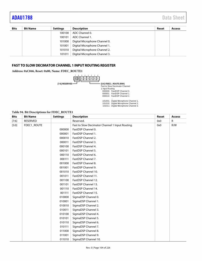
ADAU1788 Data Sheet
Rev. 0 | Page 104 of 226
Bits Bit Name Settings Description Reset Access 100100 ADC Channel 0. 100101 ADC Channel 1. 101000 Digital Microphone Channel 0. 101001 Digital Microphone Channel 1. 101010 Digital Microphone Channel 2. 101011 Digital Microphone Channel 3.
FAST TO SLOW DECIMATOR CHANNEL 1 INPUT ROUTING REGISTER Address: 0xC046, Reset: 0x00, Name: FDEC_ROUTE1
Fast to Slow Decimator Channel1 Input Routing
101011: Digital Microphone Channel 3.101010: Digital Microphone Channel 2.101001: Digital Microphone Channel 1.
...000010: FastDSP Channel 2.000001: FastDSP Channel 1.000000: FastDSP Channel 0.
0
01
02
03
04
05
06
07
0
[7:6] RESERVED [5:0] FDEC1_ROUTE (R/W)
Table 94. Bit Descriptions for FDEC_ROUTE1 Bits Bit Name Settings Description Reset Access [7:6] RESERVED Reserved. 0x0 R [5:0] FDEC1_ROUTE Fast to Slow Decimator Channel 1 Input Routing. 0x0 R/W 000000 FastDSP Channel 0. 000001 FastDSP Channel 1. 000010 FastDSP Channel 2. 000011 FastDSP Channel 3. 000100 FastDSP Channel 4. 000101 FastDSP Channel 5. 000110 FastDSP Channel 6. 000111 FastDSP Channel 7. 001000 FastDSP Channel 8. 001001 FastDSP Channel 9. 001010 FastDSP Channel 10. 001011 FastDSP Channel 11. 001100 FastDSP Channel 12. 001101 FastDSP Channel 13. 001110 FastDSP Channel 14. 001111 FastDSP Channel 15. 010000 SigmaDSP Channel 0. 010001 SigmaDSP Channel 1. 010010 SigmaDSP Channel 2. 010011 SigmaDSP Channel 3. 010100 SigmaDSP Channel 4. 010101 SigmaDSP Channel 5. 010110 SigmaDSP Channel 6. 010111 SigmaDSP Channel 7. 011000 SigmaDSP Channel 8. 011001 SigmaDSP Channel 9. 011010 SigmaDSP Channel 10.

Data Sheet ADAU1788
Rev. 0 | Page 105 of 226
Bits Bit Name Settings Description Reset Access 011011 SigmaDSP Channel 11. 011100 SigmaDSP Channel 12. 011101 SigmaDSP Channel 13. 011110 SigmaDSP Channel 14. 011111 SigmaDSP Channel 15. 100000 Input ASRC Channel 0. 100001 Input ASRC Channel 1. 100010 Input ASRC Channel 2. 100011 Input ASRC Channel 3. 100100 ADC Channel 0. 100101 ADC Channel 1. 101000 Digital Microphone Channel 0. 101001 Digital Microphone Channel 1. 101010 Digital Microphone Channel 2. 101011 Digital Microphone Channel 3.
FAST TO SLOW DECIMATOR CHANNEL 2 INPUT ROUTING REGISTER Address: 0xC047, Reset: 0x00, Name: FDEC_ROUTE2
Fast to Slow Decimator Channel2 Input Routing
101011: Digital Microphone Channel 3.101010: Digital Microphone Channel 2.101001: Digital Microphone Channel 1.
...000010: FastDSP Channel 2.000001: FastDSP Channel 1.000000: FastDSP Channel 0.
0
01
02
03
04
05
06
07
0
[7:6] RESERVED [5:0] FDEC2_ROUTE (R/W)
Table 95. Bit Descriptions for FDEC_ROUTE2 Bits Bit Name Settings Description Reset Access [7:6] RESERVED Reserved. 0x0 R [5:0] FDEC2_ROUTE Fast to Slow Decimator Channel 2 Input Routing. 0x0 R/W 000000 FastDSP Channel 0. 000001 FastDSP Channel 1. 000010 FastDSP Channel 2. 000011 FastDSP Channel 3. 000100 FastDSP Channel 4. 000101 FastDSP Channel 5. 000110 FastDSP Channel 6. 000111 FastDSP Channel 7. 001000 FastDSP Channel 8. 001001 FastDSP Channel 9. 001010 FastDSP Channel 10. 001011 FastDSP Channel 11. 001100 FastDSP Channel 12. 001101 FastDSP Channel 13. 001110 FastDSP Channel 14. 001111 FastDSP Channel 15.

ADAU1788 Data Sheet
Rev. 0 | Page 106 of 226
Bits Bit Name Settings Description Reset Access 010000 SigmaDSP Channel 0. 010001 SigmaDSP Channel 1. 010010 SigmaDSP Channel 2. 010011 SigmaDSP Channel 3. 010100 SigmaDSP Channel 4. 010101 SigmaDSP Channel 5. 010110 SigmaDSP Channel 6. 010111 SigmaDSP Channel 7. 011000 SigmaDSP Channel 8. 011001 SigmaDSP Channel 9. 011010 SigmaDSP Channel 10. 011011 SigmaDSP Channel 11. 011100 SigmaDSP Channel 12. 011101 SigmaDSP Channel 13. 011110 SigmaDSP Channel 14. 011111 SigmaDSP Channel 15. 100000 Input ASRC Channel 0. 100001 Input ASRC Channel 1. 100010 Input ASRC Channel 2. 100011 Input ASRC Channel 3. 100100 ADC Channel 0. 100101 ADC Channel 1. 101000 Digital Microphone Channel 0. 101001 Digital Microphone Channel 1. 101010 Digital Microphone Channel 2. 101011 Digital Microphone Channel 3.
FAST TO SLOW DECIMATOR CHANNEL 3 INPUT ROUTING REGISTER Address: 0xC048, Reset: 0x00, Name: FDEC_ROUTE3
Fast to Slow Decimator Channel3 Input Routing
101011: Digital Microphone Channel 3.101010: Digital Microphone Channel 2.101001: Digital Microphone Channel 1.
...000010: FastDSP Channel 2.000001: FastDSP Channel 1.000000: FastDSP Channel 0.
0
01
02
03
04
05
06
07
0
[7:6] RESERVED [5:0] FDEC3_ROUTE (R/W)
Table 96. Bit Descriptions for FDEC_ROUTE3 Bits Bit Name Settings Description Reset Access [7:6] RESERVED Reserved. 0x0 R [5:0] FDEC3_ROUTE Fast to Slow Decimator Channel 3 Input Routing. 0x0 R/W 000000 FastDSP Channel 0. 000001 FastDSP Channel 1. 000010 FastDSP Channel 2. 000011 FastDSP Channel 3. 000100 FastDSP Channel 4.

Data Sheet ADAU1788
Rev. 0 | Page 107 of 226
Bits Bit Name Settings Description Reset Access 000101 FastDSP Channel 5. 000110 FastDSP Channel 6. 000111 FastDSP Channel 7. 001000 FastDSP Channel 8. 001001 FastDSP Channel 9. 001010 FastDSP Channel 10. 001011 FastDSP Channel 11. 001100 FastDSP Channel 12. 001101 FastDSP Channel 13. 001110 FastDSP Channel 14. 001111 FastDSP Channel 15. 010000 SigmaDSP Channel 0. 010001 SigmaDSP Channel 1. 010010 SigmaDSP Channel 2. 010011 SigmaDSP Channel 3. 010100 SigmaDSP Channel 4. 010101 SigmaDSP Channel 5. 010110 SigmaDSP Channel 6. 010111 SigmaDSP Channel 7. 011000 SigmaDSP Channel 8. 011001 SigmaDSP Channel 9. 011010 SigmaDSP Channel 10. 011011 SigmaDSP Channel 11. 011100 SigmaDSP Channel 12. 011101 SigmaDSP Channel 13. 011110 SigmaDSP Channel 14. 011111 SigmaDSP Channel 15. 100000 Input ASRC Channel 0. 100001 Input ASRC Channel 1. 100010 Input ASRC Channel 2. 100011 Input ASRC Channel 3. 100100 ADC Channel 0. 100101 ADC Channel 1. 101000 Digital Microphone Channel 0. 101001 Digital Microphone Channel 1. 101010 Digital Microphone Channel 2. 101011 Digital Microphone Channel 3.
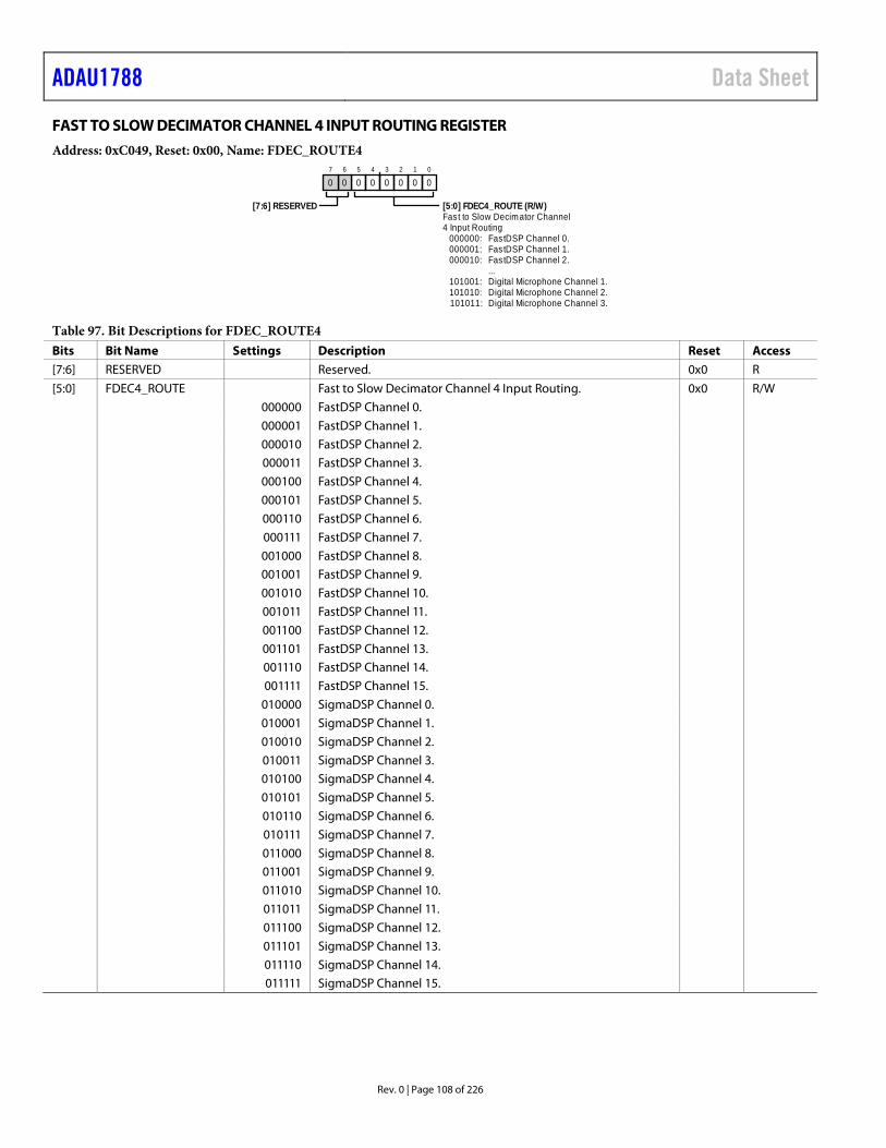
ADAU1788 Data Sheet
Rev. 0 | Page 108 of 226
FAST TO SLOW DECIMATOR CHANNEL 4 INPUT ROUTING REGISTER Address: 0xC049, Reset: 0x00, Name: FDEC_ROUTE4
Fast to Slow Decimator Channel4 Input Routing
101011: Digital Microphone Channel 3.101010: Digital Microphone Channel 2.101001: Digital Microphone Channel 1.
...000010: FastDSP Channel 2.000001: FastDSP Channel 1.000000: FastDSP Channel 0.
0
01
02
03
04
05
06
07
0
[7:6] RESERVED [5:0] FDEC4_ROUTE (R/W)
Table 97. Bit Descriptions for FDEC_ROUTE4 Bits Bit Name Settings Description Reset Access [7:6] RESERVED Reserved. 0x0 R [5:0] FDEC4_ROUTE Fast to Slow Decimator Channel 4 Input Routing. 0x0 R/W 000000 FastDSP Channel 0. 000001 FastDSP Channel 1. 000010 FastDSP Channel 2. 000011 FastDSP Channel 3. 000100 FastDSP Channel 4. 000101 FastDSP Channel 5. 000110 FastDSP Channel 6. 000111 FastDSP Channel 7. 001000 FastDSP Channel 8. 001001 FastDSP Channel 9. 001010 FastDSP Channel 10. 001011 FastDSP Channel 11. 001100 FastDSP Channel 12. 001101 FastDSP Channel 13. 001110 FastDSP Channel 14. 001111 FastDSP Channel 15. 010000 SigmaDSP Channel 0. 010001 SigmaDSP Channel 1. 010010 SigmaDSP Channel 2. 010011 SigmaDSP Channel 3. 010100 SigmaDSP Channel 4. 010101 SigmaDSP Channel 5. 010110 SigmaDSP Channel 6. 010111 SigmaDSP Channel 7. 011000 SigmaDSP Channel 8. 011001 SigmaDSP Channel 9. 011010 SigmaDSP Channel 10. 011011 SigmaDSP Channel 11. 011100 SigmaDSP Channel 12. 011101 SigmaDSP Channel 13. 011110 SigmaDSP Channel 14. 011111 SigmaDSP Channel 15.

Data Sheet ADAU1788
Rev. 0 | Page 109 of 226
Bits Bit Name Settings Description Reset Access 100000 Input ASRC Channel 0. 100001 Input ASRC Channel 1. 100010 Input ASRC Channel 2. 100011 Input ASRC Channel 3. 100100 ADC Channel 0. 100101 ADC Channel 1. 101000 Digital Microphone Channel 0. 101001 Digital Microphone Channel 1. 101010 Digital Microphone Channel 2. 101011 Digital Microphone Channel 3.
FAST TO SLOW DECIMATOR CHANNEL 5 INPUT ROUTING REGISTER Address: 0xC04A, Reset: 0x00, Name: FDEC_ROUTE5
Fast to Slow Decimator Channel5 Input Routing
101011: Digital Microphone Channel 3.101010: Digital Microphone Channel 2.101001: Digital Microphone Channel 1.
...000010: FastDSP Channel 2.000001: FastDSP Channel 1.000000: FastDSP Channel 0.
0
01
02
03
04
05
06
07
0
[7:6] RESERVED [5:0] FDEC5_ROUTE (R/W)
Table 98. Bit Descriptions for FDEC_ROUTE5 Bits Bit Name Settings Description Reset Access [7:6] RESERVED Reserved. 0x0 R [5:0] FDEC5_ROUTE Fast to Slow Decimator Channel 5 Input Routing. 0x0 R/W 000000 FastDSP Channel 0. 000001 FastDSP Channel 1. 000010 FastDSP Channel 2. 000011 FastDSP Channel 3. 000100 FastDSP Channel 4. 000101 FastDSP Channel 5. 000110 FastDSP Channel 6. 000111 FastDSP Channel 7. 001000 FastDSP Channel 8. 001001 FastDSP Channel 9. 001010 FastDSP Channel 10. 001011 FastDSP Channel 11. 001100 FastDSP Channel 12. 001101 FastDSP Channel 13. 001110 FastDSP Channel 14. 001111 FastDSP Channel 15. 010000 SigmaDSP Channel 0. 010001 SigmaDSP Channel 1. 010010 SigmaDSP Channel 2. 010011 SigmaDSP Channel 3. 010100 SigmaDSP Channel 4. 010101 SigmaDSP Channel 5. 010110 SigmaDSP Channel 6.

ADAU1788 Data Sheet
Rev. 0 | Page 110 of 226
Bits Bit Name Settings Description Reset Access 010111 SigmaDSP Channel 7. 011000 SigmaDSP Channel 8. 011001 SigmaDSP Channel 9. 011010 SigmaDSP Channel 10. 011011 SigmaDSP Channel 11. 011100 SigmaDSP Channel 12. 011101 SigmaDSP Channel 13. 011110 SigmaDSP Channel 14. 011111 SigmaDSP Channel 15. 100000 Input ASRC Channel 0. 100001 Input ASRC Channel 1. 100010 Input ASRC Channel 2. 100011 Input ASRC Channel 3. 100100 ADC Channel 0. 100101 ADC Channel 1. 101000 Digital Microphone Channel 0. 101001 Digital Microphone Channel 1. 101010 Digital Microphone Channel 2. 101011 Digital Microphone Channel 3.
FAST TO SLOW DECIMATOR CHANNEL 6 INPUT ROUTING REGISTER Address: 0xC04B, Reset: 0x00, Name: FDEC_ROUTE6
Fast to Slow Decimator Channel6 Input Routing
101011: Digital Microphone Channel 3.101010: Digital Microphone Channel 2.101001: Digital Microphone Channel 1.
...000010: FastDSP Channel 2.000001: FastDSP Channel 1.000000: FastDSP Channel 0.
0
01
02
03
04
05
06
07
0
[7:6] RESERVED [5:0] FDEC6_ROUTE (R/W)
Table 99. Bit Descriptions for FDEC_ROUTE6 Bits Bit Name Settings Description Reset Access [7:6] RESERVED Reserved. 0x0 R [5:0] FDEC6_ROUTE Fast to Slow Decimator Channel 6 Input Routing. 0x0 R/W 000000 FastDSP Channel 0. 000001 FastDSP Channel 1. 000010 FastDSP Channel 2. 000011 FastDSP Channel 3. 000100 FastDSP Channel 4. 000101 FastDSP Channel 5. 000110 FastDSP Channel 6. 000111 FastDSP Channel 7. 001000 FastDSP Channel 8. 001001 FastDSP Channel 9. 001010 FastDSP Channel 10. 001011 FastDSP Channel 11.

Data Sheet ADAU1788
Rev. 0 | Page 111 of 226
Bits Bit Name Settings Description Reset Access 001100 FastDSP Channel 12. 001101 FastDSP Channel 13. 001110 FastDSP Channel 14. 001111 FastDSP Channel 15. 010000 SigmaDSP Channel 0. 010001 SigmaDSP Channel 1. 010010 SigmaDSP Channel 2. 010011 SigmaDSP Channel 3. 010100 SigmaDSP Channel 4. 010101 SigmaDSP Channel 5. 010110 SigmaDSP Channel 6. 010111 SigmaDSP Channel 7. 011000 SigmaDSP Channel 8. 011001 SigmaDSP Channel 9. 011010 SigmaDSP Channel 10. 011011 SigmaDSP Channel 11. 011100 SigmaDSP Channel 12. 011101 SigmaDSP Channel 13. 011110 SigmaDSP Channel 14. 011111 SigmaDSP Channel 15. 100000 Input ASRC Channel 0. 100001 Input ASRC Channel 1. 100010 Input ASRC Channel 2. 100011 Input ASRC Channel 3. 100100 ADC Channel 0. 100101 ADC Channel 1. 101000 Digital Microphone Channel 0. 101001 Digital Microphone Channel 1. 101010 Digital Microphone Channel 2. 101011 Digital Microphone Channel 3.

ADAU1788 Data Sheet
Rev. 0 | Page 112 of 226
FAST TO SLOW DECIMATOR CHANNEL 7 INPUT ROUTING REGISTER Address: 0xC04C, Reset: 0x00, Name: FDEC_ROUTE7
Fast to Slow Decimator Channel7 Input Routing
101011: Digital Microphone Channel 3.101010: Digital Microphone Channel 2.101001: Digital Microphone Channel 1.
...000010: FastDSP Channel 2.000001: FastDSP Channel 1.000000: FastDSP Channel 0.
0
01
02
03
04
05
06
07
0
[7:6] RESERVED [5:0] FDEC7_ROUTE (R/W)
Table 100. Bit Descriptions for FDEC_ROUTE7 Bits Bit Name Settings Description Reset Access [7:6] RESERVED Reserved. 0x0 R [5:0] FDEC7_ROUTE Fast to Slow Decimator Channel 7 Input Routing. 0x0 R/W 000000 FastDSP Channel 0. 000001 FastDSP Channel 1. 000010 FastDSP Channel 2. 000011 FastDSP Channel 3. 000100 FastDSP Channel 4. 000101 FastDSP Channel 5. 000110 FastDSP Channel 6. 000111 FastDSP Channel 7. 001000 FastDSP Channel 8. 001001 FastDSP Channel 9. 001010 FastDSP Channel 10. 001011 FastDSP Channel 11. 001100 FastDSP Channel 12. 001101 FastDSP Channel 13. 001110 FastDSP Channel 14. 001111 FastDSP Channel 15. 010000 SigmaDSP Channel 0. 010001 SigmaDSP Channel 1. 010010 SigmaDSP Channel 2. 010011 SigmaDSP Channel 3. 010100 SigmaDSP Channel 4. 010101 SigmaDSP Channel 5. 010110 SigmaDSP Channel 6. 010111 SigmaDSP Channel 7. 011000 SigmaDSP Channel 8. 011001 SigmaDSP Channel 9. 011010 SigmaDSP Channel 10. 011011 SigmaDSP Channel 11. 011100 SigmaDSP Channel 12. 011101 SigmaDSP Channel 13. 011110 SigmaDSP Channel 14. 011111 SigmaDSP Channel 15.

Data Sheet ADAU1788
Rev. 0 | Page 113 of 226
Bits Bit Name Settings Description Reset Access 100000 Input ASRC Channel 0. 100001 Input ASRC Channel 1. 100010 Input ASRC Channel 2. 100011 Input ASRC Channel 3. 100100 ADC Channel 0. 100101 ADC Channel 1. 101000 Digital Microphone Channel 0. 101001 Digital Microphone Channel 1. 101010 Digital Microphone Channel 2. 101011 Digital Microphone Channel 3.
SLOW TO FAST INTERPOLATOR SAMPLE RATES CHANNEL 0/CHANNEL 1 REGISTER Address: 0xC04D, Reset: 0x52, Name: FINT_CTRL1
Interpolator Channel 0/Channel 1Input Sampling Rate
101: 384 kHz sample rate.100: 192 kHz sample rate.011: 96 kHz sample rate.010: 48 kHz sample rate.001: 24 kHz sample rate.000: 12 kHz sample rate.Interpolator Channel 0/Channel 1
Output Sampling Rate
110: 768 kHz sample rate.101: 384 kHz sample rate.100: 192 kHz sample rate.011: 96 kHz sample rate.010: 48 kHz sample rate.001: 24 kHz sample rate.
0
01
12
03
04
15
06
17
0
[7] RESERVED [2:0] FINT01_IN_FS (R/W)
[6:4] FINT01_OUT_FS (R/W)
[3] RESERVED
Table 101. Bit Descriptions for FINT_CTRL1 Bits Bit Name Settings Description Reset Access 7 RESERVED Reserved. 0x0 R [6:4] FINT01_OUT_FS Interpolator Channel 0/Channel 1 Output Sampling Rate. 0x5 R/W 001 24 kHz sample rate. 010 48 kHz sample rate. 011 96 kHz sample rate. 100 192 kHz sample rate. 101 384 kHz sample rate. 110 768 kHz sample rate. 3 RESERVED Reserved. 0x0 R [2:0] FINT01_IN_FS Interpolator Channel 0/Channel 1 Input Sampling Rate. 0x2 R/W 000 12 kHz sample rate. 001 24 kHz sample rate. 010 48 kHz sample rate. 011 96 kHz sample rate. 100 192 kHz sample rate. 101 384 kHz sample rate.

ADAU1788 Data Sheet
Rev. 0 | Page 114 of 226
SLOW TO FAST INTERPOLATOR SAMPLE RATES CHANNEL 2/CHANNEL 3 REGISTER Address: 0xC04E, Reset: 0x52, Name: FINT_CTRL2
Interpolator Channel 2/Channel 3Input Sampling Rate
101: 384 kHz sample rate.100: 192 kHz sample rate.011: 96 kHz sample rate.010: 48 kHz sample rate.001: 24 kHz sample rate.000: 12 kHz sample rate.Interpolator Channel 2/Channel 3
Output Sampling Rate
110: 768 kHz sample rate.101: 384 kHz sample rate.100: 192 kHz sample rate.011: 96 kHz sample rate.010: 48 kHz sample rate.001: 24 kHz sample rate.
0
01
12
03
04
15
06
17
0
[7] RESERVED [2:0] FINT23_IN_FS (R/W)
[6:4] FINT23_OUT_FS (R/W)
[3] RESERVED
Table 102. Bit Descriptions for FINT_CTRL2 Bits Bit Name Settings Description Reset Access 7 RESERVED Reserved. 0x0 R [6:4] FINT23_OUT_FS Interpolator Channel 2/Channel 3 Output Sampling Rate. 0x5 R/W 001 24 kHz sample rate. 010 48 kHz sample rate. 011 96 kHz sample rate. 100 192 kHz sample rate. 101 384 kHz sample rate. 110 768 kHz sample rate. 3 RESERVED Reserved. 0x0 R [2:0] FINT23_IN_FS Interpolator Channel 2/Channel 3 Input Sampling Rate. 0x2 R/W 000 12 kHz sample rate. 001 24 kHz sample rate. 010 48 kHz sample rate. 011 96 kHz sample rate. 100 192 kHz sample rate. 101 384 kHz sample rate.

Data Sheet ADAU1788
Rev. 0 | Page 115 of 226
SLOW TO FAST INTERPOLATOR SAMPLE RATES CHANNEL 4/CHANNEL 5 REGISTER Address: 0xC04F, Reset: 0x52, Name: FINT_CTRL3
Interpolator Channel 4/Channel 5Input Sampling Rate
101: 384 kHz sample rate.100: 192 kHz sample rate.011: 96 kHz sample rate.010: 48 kHz sample rate.001: 24 kHz sample rate.000: 12 kHz sample rate.Interpolator Channel 4/Channel 5
Output Sampling Rate
110: 768 kHz sample rate.101: 384 kHz sample rate.100: 192 kHz sample rate.011: 96 kHz sample rate.010: 48 kHz sample rate.001: 24 kHz sample rate.
0
01
12
03
04
15
06
17
0
[7] RESERVED [2:0] FINT45_IN_FS (R/W)
[6:4] FINT45_OUT_FS (R/W)
[3] RESERVED
Table 103. Bit Descriptions for FINT_CTRL3 Bits Bit Name Settings Description Reset Access 7 RESERVED Reserved. 0x0 R [6:4] FINT45_OUT_FS Interpolator Channel 4/Channel 5 Output Sampling Rate. 0x5 R/W 001 24 kHz sample rate. 010 48 kHz sample rate. 011 96 kHz sample rate. 100 192 kHz sample rate. 101 384 kHz sample rate. 110 768 kHz sample rate. 3 RESERVED Reserved. 0x0 R [2:0] FINT45_IN_FS Interpolator Channel 4/Channel 5 Input Sampling Rate. 0x2 R/W 000 12 kHz sample rate. 001 24 kHz sample rate. 010 48 kHz sample rate. 011 96 kHz sample rate. 100 192 kHz sample rate. 101 384 kHz sample rate.
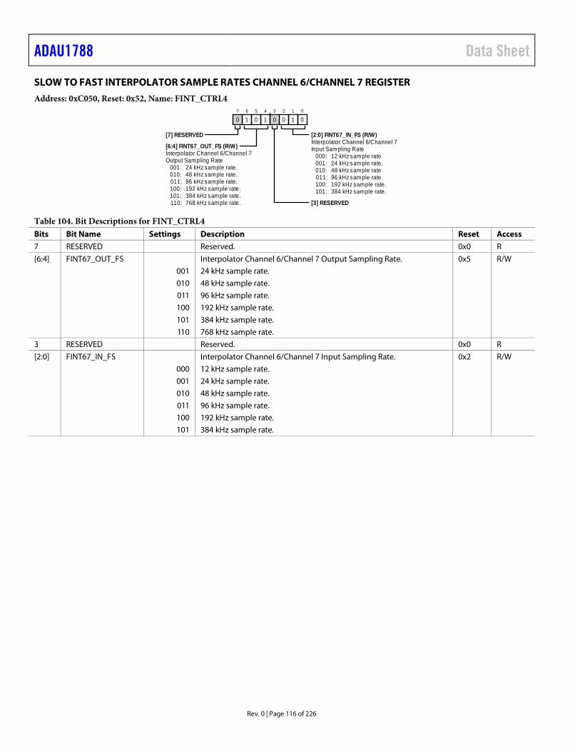
ADAU1788 Data Sheet
Rev. 0 | Page 116 of 226
SLOW TO FAST INTERPOLATOR SAMPLE RATES CHANNEL 6/CHANNEL 7 REGISTER Address: 0xC050, Reset: 0x52, Name: FINT_CTRL4
Interpolator Channel 6/Channel 7Input Sampling Rate
101: 384 kHz sample rate.100: 192 kHz sample rate.011: 96 kHz sample rate.010: 48 kHz sample rate.001: 24 kHz sample rate.000: 12 kHz sample rate.Interpolator Channel 6/Channel 7
Output Sampling Rate
110: 768 kHz sample rate.101: 384 kHz sample rate.100: 192 kHz sample rate.011: 96 kHz sample rate.010: 48 kHz sample rate.001: 24 kHz sample rate.
0
01
12
03
04
15
06
17
0
[7] RESERVED [2:0] FINT67_IN_FS (R/W)
[6:4] FINT67_OUT_FS (R/W)
[3] RESERVED
Table 104. Bit Descriptions for FINT_CTRL4 Bits Bit Name Settings Description Reset Access 7 RESERVED Reserved. 0x0 R [6:4] FINT67_OUT_FS Interpolator Channel 6/Channel 7 Output Sampling Rate. 0x5 R/W 001 24 kHz sample rate. 010 48 kHz sample rate. 011 96 kHz sample rate. 100 192 kHz sample rate. 101 384 kHz sample rate. 110 768 kHz sample rate. 3 RESERVED Reserved. 0x0 R [2:0] FINT67_IN_FS Interpolator Channel 6/Channel 7 Input Sampling Rate. 0x2 R/W 000 12 kHz sample rate. 001 24 kHz sample rate. 010 48 kHz sample rate. 011 96 kHz sample rate. 100 192 kHz sample rate. 101 384 kHz sample rate.

Data Sheet ADAU1788
Rev. 0 | Page 117 of 226
SLOW TO FAST INTERPOLATOR CHANNEL 0 INPUT ROUTING REGISTER Address: 0xC051, Reset: 0x00, Name: FINT_ROUTE0
Slow to Fast Interpolator Channel0 Input Routing
1001011: Digital Microphone Channel 3.1001010: Digital Microphone Channel 2.1001001: Digital Microphone Channel 1.
...0000010: Serial Port 0 Channel 2.0000001: Serial Port 0 Channel 1.0000000: Serial Port 0 Channel 0.
0
01
02
03
04
05
06
07
0
[7] RESERVED [6:0] FINT0_ROUTE (R/W)
Table 105. Bit Descriptions for FINT_ROUTE0 Bits Bit Name Settings Description Reset Access 7 RESERVED Reserved. 0x0 R [6:0] FINT0_ROUTE Slow to Fast Interpolator Channel 0 Input Routing. 0x0 R/W 0000000 Serial Port 0 Channel 0. 0000001 Serial Port 0 Channel 1. 0000010 Serial Port 0 Channel 2. 0000011 Serial Port 0 Channel 3. 0000100 Serial Port 0 Channel 4. 0000101 Serial Port 0 Channel 5. 0000110 Serial Port 0 Channel 6. 0000111 Serial Port 0 Channel 7. 0001000 Serial Port 0 Channel 8. 0001001 Serial Port 0 Channel 9. 0001010 Serial Port 0 Channel 10. 0001011 Serial Port 0 Channel 11. 0001100 Serial Port 0 Channel 12. 0001101 Serial Port 0 Channel 13. 0001110 Serial Port 0 Channel 14. 0001111 Serial Port 0 Channel 15. 0100000 FastDSP Channel 0. 0100001 FastDSP Channel 1. 0100010 FastDSP Channel 2. 0100011 FastDSP Channel 3. 0100100 FastDSP Channel 4. 0100101 FastDSP Channel 5. 0100110 FastDSP Channel 6. 0100111 FastDSP Channel 7. 0101000 FastDSP Channel 8. 0101001 FastDSP Channel 9. 0101010 FastDSP Channel 10. 0101011 FastDSP Channel 11. 0101100 FastDSP Channel 12. 0101101 FastDSP Channel 13. 0101110 FastDSP Channel 14. 0101111 FastDSP Channel 15.

ADAU1788 Data Sheet
Rev. 0 | Page 118 of 226
Bits Bit Name Settings Description Reset Access 0110000 SigmaDSP Channel 0. 0110001 SigmaDSP Channel 1. 0110010 SigmaDSP Channel 2. 0110011 SigmaDSP Channel 3. 0110100 SigmaDSP Channel 4. 0110101 SigmaDSP Channel 5. 0110110 SigmaDSP Channel 6. 0110111 SigmaDSP Channel 7. 0111000 SigmaDSP Channel 8. 0111001 SigmaDSP Channel 9. 0111010 SigmaDSP Channel 10. 0111011 SigmaDSP Channel 11. 0111100 SigmaDSP Channel 12. 0111101 SigmaDSP Channel 13. 0111110 SigmaDSP Channel 14. 0111111 SigmaDSP Channel 15. 1000000 Input ASRC Channel 0. 1000001 Input ASRC Channel 1. 1000010 Input ASRC Channel 2. 1000011 Input ASRC Channel 3. 1000100 ADC Channel 0. 1000101 ADC Channel 1. 1001000 Digital Microphone Channel 0. 1001001 Digital Microphone Channel 1. 1001010 Digital Microphone Channel 2. 1001011 Digital Microphone Channel 3.

Data Sheet ADAU1788
Rev. 0 | Page 119 of 226
SLOW TO FAST INTERPOLATOR CHANNEL 1 INPUT ROUTING REGISTER Address: 0xC052, Reset: 0x00, Name: FINT_ROUTE1
Slow to Fast Interpolator Channel1 Input Routing
1001011: Digital Microphone Channel 3.1001010: Digital Microphone Channel 2.1001001: Digital Microphone Channel 1.
...0000010: Serial Port 0 Channel 2.0000001: Serial Port 0 Channel 1.0000000: Serial Port 0 Channel 0.
0
01
02
03
04
05
06
07
0
[7] RESERVED [6:0] FINT1_ROUTE (R/W)
Table 106. Bit Descriptions for FINT_ROUTE1 Bits Bit Name Settings Description Reset Access 7 RESERVED Reserved. 0x0 R [6:0] FINT1_ROUTE Slow to Fast Interpolator Channel 1 Input Routing. 0x0 R/W 0000000 Serial Port 0 Channel 0. 0000001 Serial Port 0 Channel 1. 0000010 Serial Port 0 Channel 2. 0000011 Serial Port 0 Channel 3. 0000100 Serial Port 0 Channel 4. 0000101 Serial Port 0 Channel 5. 0000110 Serial Port 0 Channel 6. 0000111 Serial Port 0 Channel 7. 0001000 Serial Port 0 Channel 8. 0001001 Serial Port 0 Channel 9. 0001010 Serial Port 0 Channel 10. 0001011 Serial Port 0 Channel 11. 0001100 Serial Port 0 Channel 12. 0001101 Serial Port 0 Channel 13. 0001110 Serial Port 0 Channel 14. 0001111 Serial Port 0 Channel 15. 0100000 FastDSP Channel 0. 0100001 FastDSP Channel 1. 0100010 FastDSP Channel 2. 0100011 FastDSP Channel 3. 0100100 FastDSP Channel 4. 0100101 FastDSP Channel 5. 0100110 FastDSP Channel 6. 0100111 FastDSP Channel 7. 0101000 FastDSP Channel 8. 0101001 FastDSP Channel 9. 0101010 FastDSP Channel 10. 0101011 FastDSP Channel 11. 0101100 FastDSP Channel 12. 0101101 FastDSP Channel 13. 0101110 FastDSP Channel 14. 0101111 FastDSP Channel 15.

ADAU1788 Data Sheet
Rev. 0 | Page 120 of 226
Bits Bit Name Settings Description Reset Access 0110000 SigmaDSP Channel 0. 0110001 SigmaDSP Channel 1. 0110010 SigmaDSP Channel 2. 0110011 SigmaDSP Channel 3. 0110100 SigmaDSP Channel 4. 0110101 SigmaDSP Channel 5. 0110110 SigmaDSP Channel 6. 0110111 SigmaDSP Channel 7. 0111000 SigmaDSP Channel 8. 0111001 SigmaDSP Channel 9. 0111010 SigmaDSP Channel 10. 0111011 SigmaDSP Channel 11. 0111100 SigmaDSP Channel 12. 0111101 SigmaDSP Channel 13. 0111110 SigmaDSP Channel 14. 0111111 SigmaDSP Channel 15. 1000000 Input ASRC Channel 0. 1000001 Input ASRC Channel 1. 1000010 Input ASRC Channel 2. 1000011 Input ASRC Channel 3. 1000100 ADC Channel 0. 1000101 ADC Channel 1. 1001000 Digital Microphone Channel 0. 1001001 Digital Microphone Channel 1. 1001010 Digital Microphone Channel 2. 1001011 Digital Microphone Channel 3.
SLOW TO FAST INTERPOLATOR CHANNEL 2 INPUT ROUTING REGISTER Address: 0xC053, Reset: 0x00, Name: FINT_ROUTE2
Slow to Fast Interpolator Channel2 Input Routing
1001011: Digital Microphone Channel 3.1001010: Digital Microphone Channel 2.1001001: Digital Microphone Channel 1.
...0000010: Serial Port 0 Channel 2.0000001: Serial Port 0 Channel 1.0000000: Serial Port 0 Channel 0.
0
01
02
03
04
05
06
07
0
[7] RESERVED [6:0] FINT2_ROUTE (R/W)
Table 107. Bit Descriptions for FINT_ROUTE2 Bits Bit Name Settings Description Reset Access 7 RESERVED Reserved. 0x0 R [6:0] FINT2_ROUTE Slow to Fast Interpolator Channel 2 Input Routing. 0x0 R/W 0000000 Serial Port 0 Channel 0. 0000001 Serial Port 0 Channel 1. 0000010 Serial Port 0 Channel 2. 0000011 Serial Port 0 Channel 3. 0000100 Serial Port 0 Channel 4.
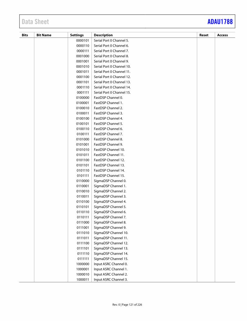
Data Sheet ADAU1788
Rev. 0 | Page 121 of 226
Bits Bit Name Settings Description Reset Access 0000101 Serial Port 0 Channel 5. 0000110 Serial Port 0 Channel 6. 0000111 Serial Port 0 Channel 7. 0001000 Serial Port 0 Channel 8. 0001001 Serial Port 0 Channel 9. 0001010 Serial Port 0 Channel 10. 0001011 Serial Port 0 Channel 11. 0001100 Serial Port 0 Channel 12. 0001101 Serial Port 0 Channel 13. 0001110 Serial Port 0 Channel 14. 0001111 Serial Port 0 Channel 15. 0100000 FastDSP Channel 0. 0100001 FastDSP Channel 1. 0100010 FastDSP Channel 2. 0100011 FastDSP Channel 3. 0100100 FastDSP Channel 4. 0100101 FastDSP Channel 5. 0100110 FastDSP Channel 6. 0100111 FastDSP Channel 7. 0101000 FastDSP Channel 8. 0101001 FastDSP Channel 9. 0101010 FastDSP Channel 10. 0101011 FastDSP Channel 11. 0101100 FastDSP Channel 12. 0101101 FastDSP Channel 13. 0101110 FastDSP Channel 14. 0101111 FastDSP Channel 15. 0110000 SigmaDSP Channel 0. 0110001 SigmaDSP Channel 1. 0110010 SigmaDSP Channel 2. 0110011 SigmaDSP Channel 3. 0110100 SigmaDSP Channel 4. 0110101 SigmaDSP Channel 5. 0110110 SigmaDSP Channel 6. 0110111 SigmaDSP Channel 7. 0111000 SigmaDSP Channel 8. 0111001 SigmaDSP Channel 9. 0111010 SigmaDSP Channel 10. 0111011 SigmaDSP Channel 11. 0111100 SigmaDSP Channel 12. 0111101 SigmaDSP Channel 13. 0111110 SigmaDSP Channel 14. 0111111 SigmaDSP Channel 15. 1000000 Input ASRC Channel 0. 1000001 Input ASRC Channel 1. 1000010 Input ASRC Channel 2. 1000011 Input ASRC Channel 3.
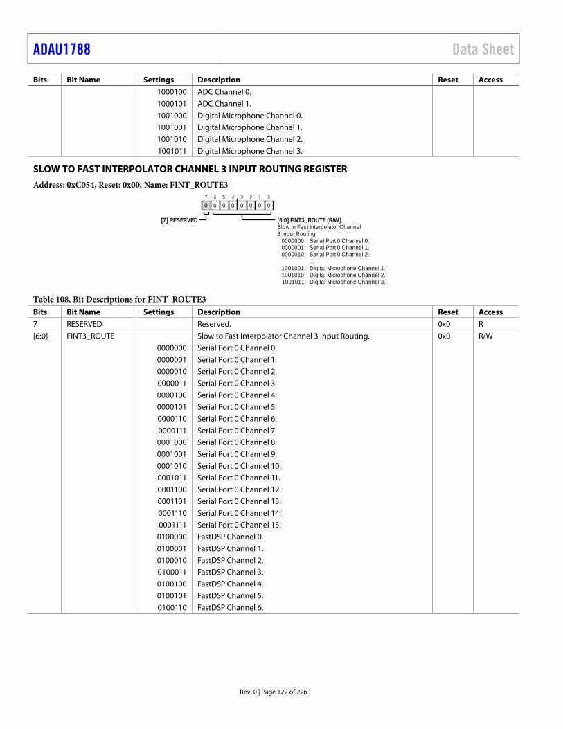
ADAU1788 Data Sheet
Rev. 0 | Page 122 of 226
Bits Bit Name Settings Description Reset Access 1000100 ADC Channel 0. 1000101 ADC Channel 1. 1001000 Digital Microphone Channel 0. 1001001 Digital Microphone Channel 1. 1001010 Digital Microphone Channel 2. 1001011 Digital Microphone Channel 3.
SLOW TO FAST INTERPOLATOR CHANNEL 3 INPUT ROUTING REGISTER Address: 0xC054, Reset: 0x00, Name: FINT_ROUTE3
Slow to Fast Interpolator Channel3 Input Routing
1001011: Digital Microphone Channel 3.1001010: Digital Microphone Channel 2.1001001: Digital Microphone Channel 1.
...0000010: Serial Port 0 Channel 2.0000001: Serial Port 0 Channel 1.0000000: Serial Port 0 Channel 0.
0
01
02
03
04
05
06
07
0
[7] RESERVED [6:0] FINT3_ROUTE (R/W)
Table 108. Bit Descriptions for FINT_ROUTE3 Bits Bit Name Settings Description Reset Access 7 RESERVED Reserved. 0x0 R [6:0] FINT3_ROUTE Slow to Fast Interpolator Channel 3 Input Routing. 0x0 R/W 0000000 Serial Port 0 Channel 0. 0000001 Serial Port 0 Channel 1. 0000010 Serial Port 0 Channel 2. 0000011 Serial Port 0 Channel 3. 0000100 Serial Port 0 Channel 4. 0000101 Serial Port 0 Channel 5. 0000110 Serial Port 0 Channel 6. 0000111 Serial Port 0 Channel 7. 0001000 Serial Port 0 Channel 8. 0001001 Serial Port 0 Channel 9. 0001010 Serial Port 0 Channel 10. 0001011 Serial Port 0 Channel 11. 0001100 Serial Port 0 Channel 12. 0001101 Serial Port 0 Channel 13. 0001110 Serial Port 0 Channel 14. 0001111 Serial Port 0 Channel 15. 0100000 FastDSP Channel 0. 0100001 FastDSP Channel 1. 0100010 FastDSP Channel 2. 0100011 FastDSP Channel 3. 0100100 FastDSP Channel 4. 0100101 FastDSP Channel 5. 0100110 FastDSP Channel 6.
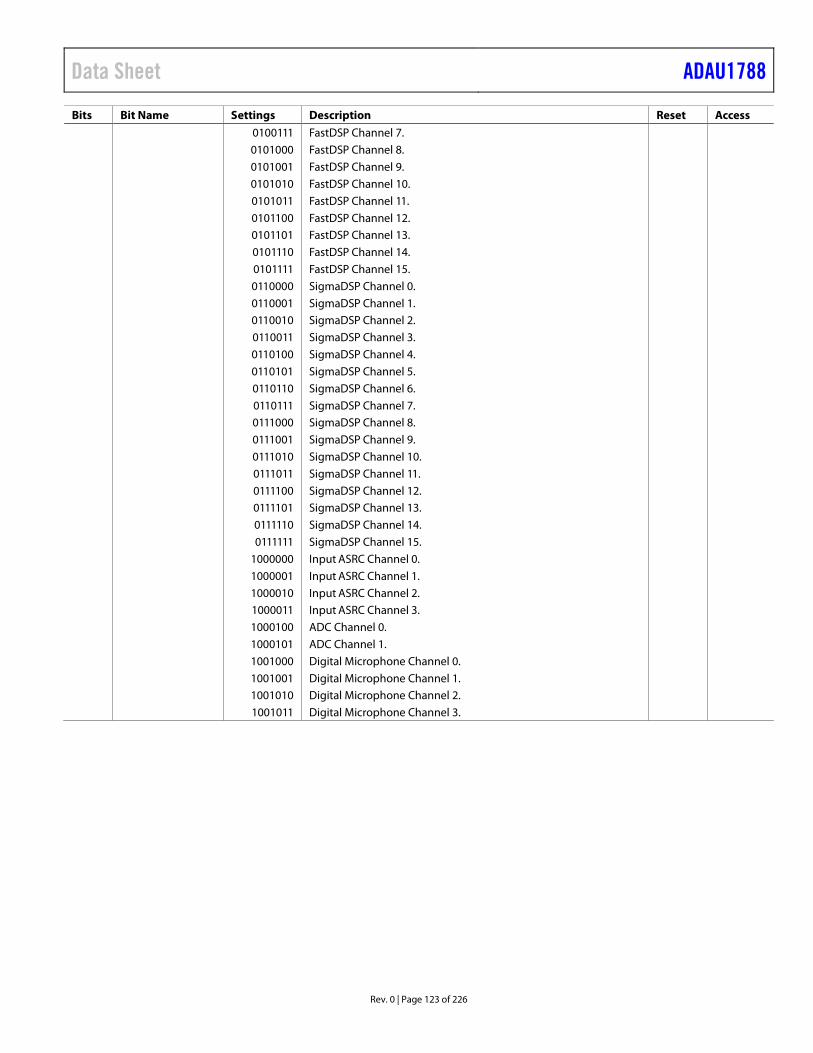
Data Sheet ADAU1788
Rev. 0 | Page 123 of 226
Bits Bit Name Settings Description Reset Access 0100111 FastDSP Channel 7. 0101000 FastDSP Channel 8. 0101001 FastDSP Channel 9. 0101010 FastDSP Channel 10. 0101011 FastDSP Channel 11. 0101100 FastDSP Channel 12. 0101101 FastDSP Channel 13. 0101110 FastDSP Channel 14. 0101111 FastDSP Channel 15. 0110000 SigmaDSP Channel 0. 0110001 SigmaDSP Channel 1. 0110010 SigmaDSP Channel 2. 0110011 SigmaDSP Channel 3. 0110100 SigmaDSP Channel 4. 0110101 SigmaDSP Channel 5. 0110110 SigmaDSP Channel 6. 0110111 SigmaDSP Channel 7. 0111000 SigmaDSP Channel 8. 0111001 SigmaDSP Channel 9. 0111010 SigmaDSP Channel 10. 0111011 SigmaDSP Channel 11. 0111100 SigmaDSP Channel 12. 0111101 SigmaDSP Channel 13. 0111110 SigmaDSP Channel 14. 0111111 SigmaDSP Channel 15. 1000000 Input ASRC Channel 0. 1000001 Input ASRC Channel 1. 1000010 Input ASRC Channel 2. 1000011 Input ASRC Channel 3. 1000100 ADC Channel 0. 1000101 ADC Channel 1. 1001000 Digital Microphone Channel 0. 1001001 Digital Microphone Channel 1. 1001010 Digital Microphone Channel 2. 1001011 Digital Microphone Channel 3.
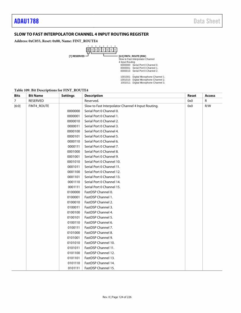
ADAU1788 Data Sheet
Rev. 0 | Page 124 of 226
SLOW TO FAST INTERPOLATOR CHANNEL 4 INPUT ROUTING REGISTER Address: 0xC055, Reset: 0x00, Name: FINT_ROUTE4
Slow to Fast Interpolator Channel4 Input Routing
1001011: Digital Microphone Channel 3.1001010: Digital Microphone Channel 2.1001001: Digital Microphone Channel 1.
...0000010: Serial Port 0 Channel 2.0000001: Serial Port 0 Channel 1.0000000: Serial Port 0 Channel 0.
0
01
02
03
04
05
06
07
0
[7] RESERVED [6:0] FINT4_ROUTE (R/W)
Table 109. Bit Descriptions for FINT_ROUTE4 Bits Bit Name Settings Description Reset Access 7 RESERVED Reserved. 0x0 R [6:0] FINT4_ROUTE Slow to Fast Interpolator Channel 4 Input Routing. 0x0 R/W 0000000 Serial Port 0 Channel 0. 0000001 Serial Port 0 Channel 1. 0000010 Serial Port 0 Channel 2. 0000011 Serial Port 0 Channel 3. 0000100 Serial Port 0 Channel 4. 0000101 Serial Port 0 Channel 5. 0000110 Serial Port 0 Channel 6. 0000111 Serial Port 0 Channel 7. 0001000 Serial Port 0 Channel 8. 0001001 Serial Port 0 Channel 9. 0001010 Serial Port 0 Channel 10. 0001011 Serial Port 0 Channel 11. 0001100 Serial Port 0 Channel 12. 0001101 Serial Port 0 Channel 13. 0001110 Serial Port 0 Channel 14. 0001111 Serial Port 0 Channel 15. 0100000 FastDSP Channel 0. 0100001 FastDSP Channel 1. 0100010 FastDSP Channel 2. 0100011 FastDSP Channel 3. 0100100 FastDSP Channel 4. 0100101 FastDSP Channel 5. 0100110 FastDSP Channel 6. 0100111 FastDSP Channel 7. 0101000 FastDSP Channel 8. 0101001 FastDSP Channel 9. 0101010 FastDSP Channel 10. 0101011 FastDSP Channel 11. 0101100 FastDSP Channel 12. 0101101 FastDSP Channel 13. 0101110 FastDSP Channel 14. 0101111 FastDSP Channel 15.

Data Sheet ADAU1788
Rev. 0 | Page 125 of 226
Bits Bit Name Settings Description Reset Access 0110000 SigmaDSP Channel 0. 0110001 SigmaDSP Channel 1. 0110010 SigmaDSP Channel 2. 0110011 SigmaDSP Channel 3. 0110100 SigmaDSP Channel 4. 0110101 SigmaDSP Channel 5. 0110110 SigmaDSP Channel 6. 0110111 SigmaDSP Channel 7. 0111000 SigmaDSP Channel 8. 0111001 SigmaDSP Channel 9. 0111010 SigmaDSP Channel 10. 0111011 SigmaDSP Channel 11. 0111100 SigmaDSP Channel 12. 0111101 SigmaDSP Channel 13. 0111110 SigmaDSP Channel 14. 0111111 SigmaDSP Channel 15. 1000000 Input ASRC Channel 0. 1000001 Input ASRC Channel 1. 1000010 Input ASRC Channel 2. 1000011 Input ASRC Channel 3. 1000100 ADC Channel 0. 1000101 ADC Channel 1. 1001000 Digital Microphone Channel 0. 1001001 Digital Microphone Channel 1. 1001010 Digital Microphone Channel 2. 1001011 Digital Microphone Channel 3.

ADAU1788 Data Sheet
Rev. 0 | Page 126 of 226
SLOW TO FAST INTERPOLATOR CHANNEL 5 INPUT ROUTING REGISTER Address: 0xC056, Reset: 0x00, Name: FINT_ROUTE5
Slow to Fast Interpolator Channel5 Input Routing
1001011: Digital Microphone Channel 3.1001010: Digital Microphone Channel 2.1001001: Digital Microphone Channel 1.
...0000010: Serial Port 0 Channel 2.0000001: Serial Port 0 Channel 1.0000000: Serial Port 0 Channel 0.
0
01
02
03
04
05
06
07
0
[7] RESERVED [6:0] FINT5_ROUTE (R/W)
Table 110. Bit Descriptions for FINT_ROUTE5 Bits Bit Name Settings Description Reset Access 7 RESERVED Reserved. 0x0 R [6:0] FINT5_ROUTE Slow to Fast Interpolator Channel 5 Input Routing. 0x0 R/W 0000000 Serial Port 0 Channel 0. 0000001 Serial Port 0 Channel 1. 0000010 Serial Port 0 Channel 2. 0000011 Serial Port 0 Channel 3. 0000100 Serial Port 0 Channel 4. 0000101 Serial Port 0 Channel 5. 0000110 Serial Port 0 Channel 6. 0000111 Serial Port 0 Channel 7. 0001000 Serial Port 0 Channel 8. 0001001 Serial Port 0 Channel 9. 0001010 Serial Port 0 Channel 10. 0001011 Serial Port 0 Channel 11. 0001100 Serial Port 0 Channel 12. 0001101 Serial Port 0 Channel 13. 0001110 Serial Port 0 Channel 14. 0001111 Serial Port 0 Channel 15. 0100000 FastDSP Channel 0. 0100001 FastDSP Channel 1. 0100010 FastDSP Channel 2. 0100011 FastDSP Channel 3. 0100100 FastDSP Channel 4. 0100101 FastDSP Channel 5. 0100110 FastDSP Channel 6. 0100111 FastDSP Channel 7. 0101000 FastDSP Channel 8. 0101001 FastDSP Channel 9. 0101010 FastDSP Channel 10. 0101011 FastDSP Channel 11. 0101100 FastDSP Channel 12. 0101101 FastDSP Channel 13. 0101110 FastDSP Channel 14. 0101111 FastDSP Channel 15.

Data Sheet ADAU1788
Rev. 0 | Page 127 of 226
Bits Bit Name Settings Description Reset Access 0110000 SigmaDSP Channel 0. 0110001 SigmaDSP Channel 1. 0110010 SigmaDSP Channel 2. 0110011 SigmaDSP Channel 3. 0110100 SigmaDSP Channel 4. 0110101 SigmaDSP Channel 5. 0110110 SigmaDSP Channel 6. 0110111 SigmaDSP Channel 7. 0111000 SigmaDSP Channel 8. 0111001 SigmaDSP Channel 9. 0111010 SigmaDSP Channel 10. 0111011 SigmaDSP Channel 11. 0111100 SigmaDSP Channel 12. 0111101 SigmaDSP Channel 13. 0111110 SigmaDSP Channel 14. 0111111 SigmaDSP Channel 15. 1000000 Input ASRC Channel 0. 1000001 Input ASRC Channel 1. 1000010 Input ASRC Channel 2. 1000011 Input ASRC Channel 3. 1000100 ADC Channel 0. 1000101 ADC Channel 1. 1001000 Digital Microphone Channel 0. 1001001 Digital Microphone Channel 1. 1001010 Digital Microphone Channel 2. 1001011 Digital Microphone Channel 3.

ADAU1788 Data Sheet
Rev. 0 | Page 128 of 226
SLOW TO FAST INTERPOLATOR CHANNEL 6 INPUT ROUTING REGISTER Address: 0xC057, Reset: 0x00, Name: FINT_ROUTE6
Slow to Fast Interpolator Channel6 Input Routing
1001011: Digital Microphone Channel 3.1001010: Digital Microphone Channel 2.1001001: Digital Microphone Channel 1.
...0000010: Serial Port 0 Channel 2.0000001: Serial Port 0 Channel 1.0000000: Serial Port 0 Channel 0.
0
01
02
03
04
05
06
07
0
[7] RESERVED [6:0] FINT6_ROUTE (R/W)
Table 111. Bit Descriptions for FINT_ROUTE6 Bits Bit Name Settings Description Reset Access 7 RESERVED Reserved. 0x0 R [6:0] FINT6_ROUTE Slow to Fast Interpolator Channel 6 Input Routing. 0x0 R/W 0000000 Serial Port 0 Channel 0. 0000001 Serial Port 0 Channel 1. 0000010 Serial Port 0 Channel 2. 0000011 Serial Port 0 Channel 3. 0000100 Serial Port 0 Channel 4. 0000101 Serial Port 0 Channel 5. 0000110 Serial Port 0 Channel 6. 0000111 Serial Port 0 Channel 7. 0001000 Serial Port 0 Channel 8. 0001001 Serial Port 0 Channel 9. 0001010 Serial Port 0 Channel 10. 0001011 Serial Port 0 Channel 11. 0001100 Serial Port 0 Channel 12. 0001101 Serial Port 0 Channel 13. 0001110 Serial Port 0 Channel 14. 0001111 Serial Port 0 Channel 15. 0100000 FastDSP Channel 0. 0100001 FastDSP Channel 1. 0100010 FastDSP Channel 2. 0100011 FastDSP Channel 3. 0100100 FastDSP Channel 4. 0100101 FastDSP Channel 5. 0100110 FastDSP Channel 6. 0100111 FastDSP Channel 7. 0101000 FastDSP Channel 8. 0101001 FastDSP Channel 9. 0101010 FastDSP Channel 10. 0101011 FastDSP Channel 11. 0101100 FastDSP Channel 12. 0101101 FastDSP Channel 13. 0101110 FastDSP Channel 14. 0101111 FastDSP Channel 15.

Data Sheet ADAU1788
Rev. 0 | Page 129 of 226
Bits Bit Name Settings Description Reset Access 0110000 SigmaDSP Channel 0. 0110001 SigmaDSP Channel 1. 0110010 SigmaDSP Channel 2. 0110011 SigmaDSP Channel 3. 0110100 SigmaDSP Channel 4. 0110101 SigmaDSP Channel 5. 0110110 SigmaDSP Channel 6. 0110111 SigmaDSP Channel 7. 0111000 SigmaDSP Channel 8. 0111001 SigmaDSP Channel 9. 0111010 SigmaDSP Channel 10. 0111011 SigmaDSP Channel 11. 0111100 SigmaDSP Channel 12. 0111101 SigmaDSP Channel 13. 0111110 SigmaDSP Channel 14. 0111111 SigmaDSP Channel 15. 1000000 Input ASRC Channel 0. 1000001 Input ASRC Channel 1. 1000010 Input ASRC Channel 2. 1000011 Input ASRC Channel 3. 1000100 ADC Channel 0. 1000101 ADC Channel 1. 1001000 Digital Microphone Channel 0. 1001001 Digital Microphone Channel 1. 1001010 Digital Microphone Channel 2. 1001011 Digital Microphone Channel 3.

ADAU1788 Data Sheet
Rev. 0 | Page 130 of 226
SLOW TO FAST INTERPOLATOR CHANNEL 7 INPUT ROUTING REGISTER Address: 0xC058, Reset: 0x00, Name: FINT_ROUTE7
Slow to Fast Interpolator Channel7 Input Routing
1001011: Digital Microphone Channel 3.1001010: Digital Microphone Channel 2.1001001: Digital Microphone Channel 1.
...0000010: Serial Port 0 Channel 2.0000001: Serial Port 0 Channel 1.0000000: Serial Port 0 Channel 0.
0
01
02
03
04
05
06
07
0
[7] RESERVED [6:0] FINT7_ROUTE (R/W)
Table 112. Bit Descriptions for FINT_ROUTE7 Bits Bit Name Settings Description Reset Access 7 RESERVED Reserved. 0x0 R [6:0] FINT7_ROUTE Slow to Fast Interpolator Channel 7 Input Routing. 0x0 R/W 0000000 Serial Port 0 Channel 0. 0000001 Serial Port 0 Channel 1. 0000010 Serial Port 0 Channel 2. 0000011 Serial Port 0 Channel 3. 0000100 Serial Port 0 Channel 4. 0000101 Serial Port 0 Channel 5. 0000110 Serial Port 0 Channel 6. 0000111 Serial Port 0 Channel 7. 0001000 Serial Port 0 Channel 8. 0001001 Serial Port 0 Channel 9. 0001010 Serial Port 0 Channel 10. 0001011 Serial Port 0 Channel 11. 0001100 Serial Port 0 Channel 12. 0001101 Serial Port 0 Channel 13. 0001110 Serial Port 0 Channel 14. 0001111 Serial Port 0 Channel 15. 0100000 FastDSP Channel 0. 0100001 FastDSP Channel 1. 0100010 FastDSP Channel 2. 0100011 FastDSP Channel 3. 0100100 FastDSP Channel 4. 0100101 FastDSP Channel 5. 0100110 FastDSP Channel 6. 0100111 FastDSP Channel 7. 0101000 FastDSP Channel 8. 0101001 FastDSP Channel 9. 0101010 FastDSP Channel 10. 0101011 FastDSP Channel 11. 0101100 FastDSP Channel 12. 0101101 FastDSP Channel 13. 0101110 FastDSP Channel 14. 0101111 FastDSP Channel 15.

Data Sheet ADAU1788
Rev. 0 | Page 131 of 226
Bits Bit Name Settings Description Reset Access 0110000 SigmaDSP Channel 0. 0110001 SigmaDSP Channel 1. 0110010 SigmaDSP Channel 2. 0110011 SigmaDSP Channel 3. 0110100 SigmaDSP Channel 4. 0110101 SigmaDSP Channel 5. 0110110 SigmaDSP Channel 6. 0110111 SigmaDSP Channel 7. 0111000 SigmaDSP Channel 8. 0111001 SigmaDSP Channel 9. 0111010 SigmaDSP Channel 10. 0111011 SigmaDSP Channel 11. 0111100 SigmaDSP Channel 12. 0111101 SigmaDSP Channel 13. 0111110 SigmaDSP Channel 14. 0111111 SigmaDSP Channel 15. 1000000 Input ASRC Channel 0. 1000001 Input ASRC Channel 1. 1000010 Input ASRC Channel 2. 1000011 Input ASRC Channel 3. 1000100 ADC Channel 0. 1000101 ADC Channel 1. 1001000 Digital Microphone Channel 0. 1001001 Digital Microphone Channel 1. 1001010 Digital Microphone Channel 2. 1001011 Digital Microphone Channel 3.

ADAU1788 Data Sheet
Rev. 0 | Page 132 of 226
INPUT ASRC CONTROL, SOURCE, AND RATE SELECTION REGISTER Address: 0xC059, Reset: 0x02, Name: ASRCI_CTRL
Input ASRC Additional Filtering Enable
1: Voice band filter on.0: No additional voice band filter.
Input ASRC Sample Rate Selection
100: 192 kHz sample rate.011: 96 kHz sample rate.010: 48 kHz sample rate.001: 24 kHz sample rate.000: 12 kHz sample rate.
Input ASRC Voice Filter Enable
1: Voice filter on.0: Voice filter off.
Input ASRC Low Power Mode Selection.Even lower power.
1: Low power mode.0: High performance mode.Input ASRC Low Power Mode Selection
1: Low power mode.0: High performance mode.
0
01
12
03
04
05
06
07
0
[7] ASRCI_MORE_FILT (R/W) [2:0] ASRCI_OUT_FS (R/W)
[6] ASRCI_VFILT (R/W)
[3] ASRCI_LPM_II (R/W)
[5] ASRCI_LPM (R/W)
[4] RESERVED
Table 113. Bit Descriptions for ASRCI_CTRL Bits Bit Name Settings Description Reset Access 7 ASRCI_MORE_FILT Input ASRC Additional Filtering Enable. This bit can enable additional filtering
within the ASRC that can provide higher performance under some conditions. 0x0 R/W
0 No additional voice band filter. 1 Voice band filter on. 6 ASRCI_VFILT Input ASRC Voice Filter Enable. 0x0 R/W 0 Voice filter off. 1 Voice filter on. 5 ASRCI_LPM Input ASRC Low Power Mode Selection. 0x0 R/W 0 High performance mode. 1 Low power mode. 4 RESERVED Reserved. 0x0 R/W 3 ASRCI_LPM_II Input ASRC Low Power Mode Selection. Even lower power. 0x0 R/W 0 High performance mode. 1 Low power mode. [2:0] ASRCI_OUT_FS Input ASRC Sample Rate Selection. 0x2 R/W 000 12 kHz sample rate. 001 24 kHz sample rate. 010 48 kHz sample rate. 011 96 kHz sample rate. 100 192 kHz sample rate.

Data Sheet ADAU1788
Rev. 0 | Page 133 of 226
INPUT ASRC CHANNEL 0 AND CHANNEL 1 INPUT ROUTING REGISTER Address: 0xC05A, Reset: 0x00, Name: ASRCI_ROUTE01
Input ASRC Channel 1 Routing
1111: Serial Port Channel 15.1110: Serial Port Channel 14.1101: Serial Port Channel 13.
...0010: Serial Port Channel 2.0001: Serial Port Channel 1.0000: Serial Port Channel 0.
Input ASRC Channel 0 Routing
1111: Serial Port Channel 15.1110: Serial Port Channel 14.1101: Serial Port Channel 13.
...0010: Serial Port Channel 2.0001: Serial Port Channel 1.0000: Serial Port Channel 0.
0
01
02
03
04
05
06
07
0
[7:4] ASRCI1_ROUTE (R/W) [3:0] ASRCI0_ROUTE (R/W)
Table 114. Bit Descriptions for ASRCI_ROUTE01 Bits Bit Name Settings Description Reset Access [7:4] ASRCI1_ROUTE Input ASRC Channel 1 Routing. 0x0 R/W 0000 Serial Port Channel 0. 0001 Serial Port Channel 1. 0010 Serial Port Channel 2. 0011 Serial Port Channel 3. 0100 Serial Port Channel 4. 0101 Serial Port Channel 5. 0110 Serial Port Channel 6. 0111 Serial Port Channel 7. 1000 Serial Port Channel 8. 1001 Serial Port Channel 9. 1010 Serial Port Channel 10. 1011 Serial Port Channel 11. 1100 Serial Port Channel 12. 1101 Serial Port Channel 13. 1110 Serial Port Channel 14. 1111 Serial Port Channel 15. [3:0] ASRCI0_ROUTE Input ASRC Channel 0 Routing. 0x0 R/W 0000 Serial Port Channel 0. 0001 Serial Port Channel 1. 0010 Serial Port Channel 2. 0011 Serial Port Channel 3. 0100 Serial Port Channel 4. 0101 Serial Port Channel 5. 0110 Serial Port Channel 6. 0111 Serial Port Channel 7. 1000 Serial Port Channel 8. 1001 Serial Port Channel 9. 1010 Serial Port Channel 10. 1011 Serial Port Channel 11. 1100 Serial Port Channel 12. 1101 Serial Port Channel 13. 1110 Serial Port Channel 14. 1111 Serial Port Channel 15.

ADAU1788 Data Sheet
Rev. 0 | Page 134 of 226
INPUT ASRC CHANNEL 2 AND CHANNEL 3 INPUT ROUTING REGISTER Address: 0xC05B, Reset: 0x00, Name: ASRCI_ROUTE23
Input ASRC Channel 3 Routing
1111: Serial Port Channel 15.1110: Serial Port Channel 14.1101: Serial Port Channel 13.
...0010: Serial Port Channel 2.0001: Serial Port Channel 1.0000: Serial Port Channel 0.
Input ASRC Channel 2 Routing
1111: Serial Port Channel 15.1110: Serial Port Channel 14.1101: Serial Port Channel 13.
...0010: Serial Port Channel 2.0001: Serial Port Channel 1.0000: Serial Port Channel 0.
0
01
02
03
04
05
06
07
0
[7:4] ASRCI3_ROUTE (R/W) [3:0] ASRCI2_ROUTE (R/W)
Table 115. Bit Descriptions for ASRCI_ROUTE23 Bits Bit Name Settings Description Reset Access [7:4] ASRCI3_ROUTE Input ASRC Channel 3 Routing. 0x0 R/W 0000 Serial Port Channel 0. 0001 Serial Port Channel 1. 0010 Serial Port Channel 2. 0011 Serial Port Channel 3. 0100 Serial Port Channel 4. 0101 Serial Port Channel 5. 0110 Serial Port Channel 6. 0111 Serial Port Channel 7. 1000 Serial Port Channel 8. 1001 Serial Port Channel 9. 1010 Serial Port Channel 10. 1011 Serial Port Channel 11. 1100 Serial Port Channel 12. 1101 Serial Port Channel 13. 1110 Serial Port Channel 14. 1111 Serial Port Channel 15. [3:0] ASRCI2_ROUTE Input ASRC Channel 2 Routing. 0x0 R/W 0000 Serial Port Channel 0. 0001 Serial Port Channel 1. 0010 Serial Port Channel 2. 0011 Serial Port Channel 3. 0100 Serial Port Channel 4. 0101 Serial Port Channel 5. 0110 Serial Port Channel 6. 0111 Serial Port Channel 7. 1000 Serial Port Channel 8. 1001 Serial Port Channel 9. 1010 Serial Port Channel 10. 1011 Serial Port Channel 11. 1100 Serial Port Channel 12. 1101 Serial Port Channel 13. 1110 Serial Port Channel 14. 1111 Serial Port Channel 15.

Data Sheet ADAU1788
Rev. 0 | Page 135 of 226
OUTPUT ASRC CONTROL REGISTER Address: 0xC05C, Reset: 0x02, Name: ASRCO_CTRL
Output ASRC Additional Filtering Enable
1: Voice band filter on.0: No additional voice band filter.
Output ASRC Input Sample RateSelection
100: 192 kHz sample rate.011: 96 kHz sample rate.010: 48 kHz sample rate.001: 24 kHz sample rate.000: 12 kHz sample rate.
Output ASRC Voice Filter Enable
1: Voice filter on.0: Voice filter off.
Output ASRC Low Power Mode Selection.Even lower power.
1: Low power mode.0: High performance mode.
Output ASRC Low Power Mode Selection
1: Low power mode.0: High performance mode.
0
01
12
03
04
05
06
07
0
[7] ASRCO_MORE_FILT (R/W) [2:0] ASRCO_IN_FS (R/W)
[6] ASRCO_VFILT (R/W)
[3] ASRCO_LPM_II (R/W)[5] ASRCO_LPM (R/W)
[4] RESERVED
Table 116. Bit Descriptions for ASRCO_CTRL Bits Bit Name Settings Description Reset Access 7 ASRCO_MORE_FILT Output ASRC Additional Filtering Enable. This bit can enable additional filtering
within the ASRC that can provide higher performance under some conditions. 0x0 R/W
0 No additional voice band filter. 1 Voice band filter on. 6 ASRCO_VFILT Output ASRC Voice Filter Enable. 0x0 R/W 0 Voice filter off. 1 Voice filter on. 5 ASRCO_LPM Output ASRC Low Power Mode Selection. 0x0 R/W 0 High performance mode. 1 Low power mode. 4 RESERVED Reserved. 0x0 R/W 3 ASRCO_LPM_II Output ASRC Low Power Mode Selection. Even lower power. 0x0 R/W 0 High performance mode. 1 Low power mode. [2:0] ASRCO_IN_FS Output ASRC Input Sample Rate Selection. 0x2 R/W 000 12 kHz sample rate. 001 24 kHz sample rate. 010 48 kHz sample rate. 011 96 kHz sample rate. 100 192 kHz sample rate.

ADAU1788 Data Sheet
Rev. 0 | Page 136 of 226
OUTPUT ASRC CHANNEL 0 INPUT ROUTING REGISTER Address: 0xC05D, Reset: 0x00, Name: ASRCO_ROUTE0
Output ASRC Channel 0 Input Routing
110011: Fast to Slow Decimator Channel 7.110010: Fast to Slow Decimator Channel 6.110001: Fast to Slow Decimator Channel 5.
...000010: FastDSP Channel 2.000001: FastDSP Channel 1.000000: FastDSP Channel 0.
0
01
02
03
04
05
06
07
0
[7:6] RESERVED [5:0] ASRCO0_ROUTE (R/W)
Table 117. Bit Descriptions for ASRCO_ROUTE0 Bits Bit Name Settings Description Reset Access [7:6] RESERVED Reserved. 0x0 R [5:0] ASRCO0_ROUTE Output ASRC Channel 0 Input Routing. 0x0 R/W 000000 FastDSP Channel 0. 000001 FastDSP Channel 1. 000010 FastDSP Channel 2. 000011 FastDSP Channel 3. 000100 FastDSP Channel 4. 000101 FastDSP Channel 5. 000110 FastDSP Channel 6. 000111 FastDSP Channel 7. 001000 FastDSP Channel 8. 001001 FastDSP Channel 9. 001010 FastDSP Channel 10. 001011 FastDSP Channel 11. 001100 FastDSP Channel 12. 001101 FastDSP Channel 13. 001110 FastDSP Channel 14. 001111 FastDSP Channel 15. 010000 SigmaDSP Channel 0. 010001 SigmaDSP Channel 1. 010010 SigmaDSP Channel 2. 010011 SigmaDSP Channel 3. 010100 SigmaDSP Channel 4. 010101 SigmaDSP Channel 5. 010110 SigmaDSP Channel 6. 010111 SigmaDSP Channel 7. 011000 SigmaDSP Channel 8. 011001 SigmaDSP Channel 9. 011010 SigmaDSP Channel 10. 011011 SigmaDSP Channel 11. 011100 SigmaDSP Channel 12. 011101 SigmaDSP Channel 13. 011110 SigmaDSP Channel 14. 011111 SigmaDSP Channel 15. 100000 ADC Channel 0. 100001 ADC Channel 1.
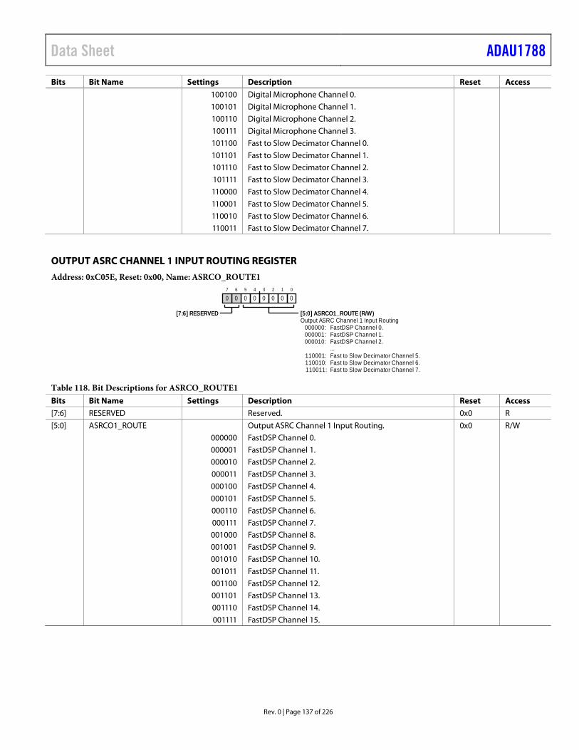
Data Sheet ADAU1788
Rev. 0 | Page 137 of 226
Bits Bit Name Settings Description Reset Access 100100 Digital Microphone Channel 0. 100101 Digital Microphone Channel 1. 100110 Digital Microphone Channel 2. 100111 Digital Microphone Channel 3. 101100 Fast to Slow Decimator Channel 0. 101101 Fast to Slow Decimator Channel 1. 101110 Fast to Slow Decimator Channel 2. 101111 Fast to Slow Decimator Channel 3. 110000 Fast to Slow Decimator Channel 4. 110001 Fast to Slow Decimator Channel 5. 110010 Fast to Slow Decimator Channel 6. 110011 Fast to Slow Decimator Channel 7.
OUTPUT ASRC CHANNEL 1 INPUT ROUTING REGISTER Address: 0xC05E, Reset: 0x00, Name: ASRCO_ROUTE1
Output ASRC Channel 1 Input Routing
110011: Fast to Slow Decimator Channel 7.110010: Fast to Slow Decimator Channel 6.110001: Fast to Slow Decimator Channel 5.
...000010: FastDSP Channel 2.000001: FastDSP Channel 1.000000: FastDSP Channel 0.
0
01
02
03
04
05
06
07
0
[7:6] RESERVED [5:0] ASRCO1_ROUTE (R/W)
Table 118. Bit Descriptions for ASRCO_ROUTE1 Bits Bit Name Settings Description Reset Access [7:6] RESERVED Reserved. 0x0 R [5:0] ASRCO1_ROUTE Output ASRC Channel 1 Input Routing. 0x0 R/W 000000 FastDSP Channel 0. 000001 FastDSP Channel 1. 000010 FastDSP Channel 2. 000011 FastDSP Channel 3. 000100 FastDSP Channel 4. 000101 FastDSP Channel 5. 000110 FastDSP Channel 6. 000111 FastDSP Channel 7. 001000 FastDSP Channel 8. 001001 FastDSP Channel 9. 001010 FastDSP Channel 10. 001011 FastDSP Channel 11. 001100 FastDSP Channel 12. 001101 FastDSP Channel 13. 001110 FastDSP Channel 14. 001111 FastDSP Channel 15.

ADAU1788 Data Sheet
Rev. 0 | Page 138 of 226
Bits Bit Name Settings Description Reset Access 010000 SigmaDSP Channel 0. 010001 SigmaDSP Channel 1. 010010 SigmaDSP Channel 2. 010011 SigmaDSP Channel 3. 010100 SigmaDSP Channel 4. 010101 SigmaDSP Channel 5. 010110 SigmaDSP Channel 6. 010111 SigmaDSP Channel 7. 011000 SigmaDSP Channel 8. 011001 SigmaDSP Channel 9. 011010 SigmaDSP Channel 10. 011011 SigmaDSP Channel 11. 011100 SigmaDSP Channel 12. 011101 SigmaDSP Channel 13. 011110 SigmaDSP Channel 14. 011111 SigmaDSP Channel 15. 100000 ADC Channel 0. 100001 ADC Channel 1. 100100 Digital Microphone Channel 0. 100101 Digital Microphone Channel 1. 100110 Digital Microphone Channel 2. 100111 Digital Microphone Channel 3. 101100 Fast to Slow Decimator Channel 0. 101101 Fast to Slow Decimator Channel 1. 101110 Fast to Slow Decimator Channel 2. 101111 Fast to Slow Decimator Channel 3. 110000 Fast to Slow Decimator Channel 4. 110001 Fast to Slow Decimator Channel 5. 110010 Fast to Slow Decimator Channel 6. 110011 Fast to Slow Decimator Channel 7.

Data Sheet ADAU1788
Rev. 0 | Page 139 of 226
OUTPUT ASRC CHANNEL 2 INPUT ROUTING REGISTER Address: 0xC05F, Reset: 0x00, Name: ASRCO_ROUTE2
Output ASRC Channel 2 Input Routing
110011: Fast to Slow Decimator Channel 7.110010: Fast to Slow Decimator Channel 6.110001: Fast to Slow Decimator Channel 5.
...000010: FastDSP Channel 2.000001: FastDSP Channel 1.000000: FastDSP Channel 0.
0
01
02
03
04
05
06
07
0
[7:6] RESERVED [5:0] ASRCO2_ROUTE (R/W)
Table 119. Bit Descriptions for ASRCO_ROUTE2 Bits Bit Name Settings Description Reset Access [7:6] RESERVED Reserved. 0x0 R [5:0] ASRCO2_ROUTE Output ASRC Channel 2 Input Routing. 0x0 R/W 000000 FastDSP Channel 0. 000001 FastDSP Channel 1. 000010 FastDSP Channel 2. 000011 FastDSP Channel 3. 000100 FastDSP Channel 4. 000101 FastDSP Channel 5. 000110 FastDSP Channel 6. 000111 FastDSP Channel 7. 001000 FastDSP Channel 8. 001001 FastDSP Channel 9. 001010 FastDSP Channel 10. 001011 FastDSP Channel 11. 001100 FastDSP Channel 12. 001101 FastDSP Channel 13. 001110 FastDSP Channel 14. 001111 FastDSP Channel 15. 010000 SigmaDSP Channel 0. 010001 SigmaDSP Channel 1. 010010 SigmaDSP Channel 2. 010011 SigmaDSP Channel 3. 010100 SigmaDSP Channel 4. 010101 SigmaDSP Channel 5. 010110 SigmaDSP Channel 6. 010111 SigmaDSP Channel 7. 011000 SigmaDSP Channel 8. 011001 SigmaDSP Channel 9. 011010 SigmaDSP Channel 10. 011011 SigmaDSP Channel 11. 011100 SigmaDSP Channel 12. 011101 SigmaDSP Channel 13. 011110 SigmaDSP Channel 14. 011111 SigmaDSP Channel 15. 100000 ADC Channel 0. 100001 ADC Channel 1.

ADAU1788 Data Sheet
Rev. 0 | Page 140 of 226
Bits Bit Name Settings Description Reset Access 100100 Digital Microphone Channel 0. 100101 Digital Microphone Channel 1. 100110 Digital Microphone Channel 2. 100111 Digital Microphone Channel 3. 101100 Fast to Slow Decimator Channel 0. 101101 Fast to Slow Decimator Channel 1. 101110 Fast to Slow Decimator Channel 2. 101111 Fast to Slow Decimator Channel 3. 110000 Fast to Slow Decimator Channel 4. 110001 Fast to Slow Decimator Channel 5. 110010 Fast to Slow Decimator Channel 6. 110011 Fast to Slow Decimator Channel 7.
OUTPUT ASRC CHANNEL 3 INPUT ROUTING REGISTER Address: 0xC060, Reset: 0x00, Name: ASRCO_ROUTE3
Output ASRC Channel 3 Input Routing
110011: Fast to Slow Decimator Channel 7.110010: Fast to Slow Decimator Channel 6.110001: Fast to Slow Decimator Channel 5.
...000010: FastDSP Channel 2.000001: FastDSP Channel 1.000000: FastDSP Channel 0.
0
01
02
03
04
05
06
07
0
[7:6] RESERVED [5:0] ASRCO3_ROUTE (R/W)
Table 120. Bit Descriptions for ASRCO_ROUTE3 Bits Bit Name Settings Description Reset Access [7:6] RESERVED Reserved. 0x0 R [5:0] ASRCO3_ROUTE Output ASRC Channel 3 Input Routing. 0x0 R/W 000000 FastDSP Channel 0. 000001 FastDSP Channel 1. 000010 FastDSP Channel 2. 000011 FastDSP Channel 3. 000100 FastDSP Channel 4. 000101 FastDSP Channel 5. 000110 FastDSP Channel 6. 000111 FastDSP Channel 7. 001000 FastDSP Channel 8. 001001 FastDSP Channel 9. 001010 FastDSP Channel 10. 001011 FastDSP Channel 11. 001100 FastDSP Channel 12. 001101 FastDSP Channel 13. 001110 FastDSP Channel 14. 001111 FastDSP Channel 15. 010000 SigmaDSP Channel 0. 010001 SigmaDSP Channel 1. 010010 SigmaDSP Channel 2. 010011 SigmaDSP Channel 3. 010100 SigmaDSP Channel 4. 010101 SigmaDSP Channel 5.
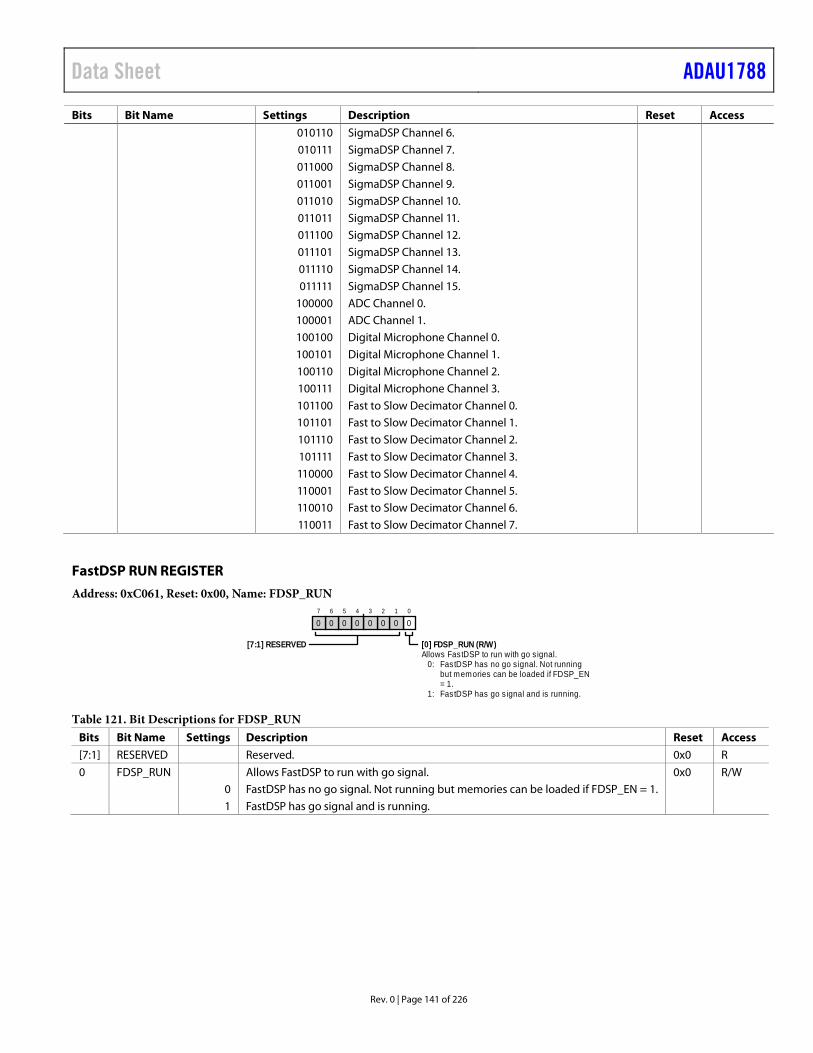
Data Sheet ADAU1788
Rev. 0 | Page 141 of 226
Bits Bit Name Settings Description Reset Access 010110 SigmaDSP Channel 6. 010111 SigmaDSP Channel 7. 011000 SigmaDSP Channel 8. 011001 SigmaDSP Channel 9. 011010 SigmaDSP Channel 10. 011011 SigmaDSP Channel 11. 011100 SigmaDSP Channel 12. 011101 SigmaDSP Channel 13. 011110 SigmaDSP Channel 14. 011111 SigmaDSP Channel 15. 100000 ADC Channel 0. 100001 ADC Channel 1. 100100 Digital Microphone Channel 0. 100101 Digital Microphone Channel 1. 100110 Digital Microphone Channel 2. 100111 Digital Microphone Channel 3. 101100 Fast to Slow Decimator Channel 0. 101101 Fast to Slow Decimator Channel 1. 101110 Fast to Slow Decimator Channel 2. 101111 Fast to Slow Decimator Channel 3. 110000 Fast to Slow Decimator Channel 4. 110001 Fast to Slow Decimator Channel 5. 110010 Fast to Slow Decimator Channel 6. 110011 Fast to Slow Decimator Channel 7.
FastDSP RUN REGISTER Address: 0xC061, Reset: 0x00, Name: FDSP_RUN
Allows FastDSP to run with go s ignal.
1: FastDSP has go s ignal and is running.
0:
= 1.but memories can be loaded if FDSP_ENFastDSP has no go s ignal. Not running
0
01
02
03
04
05
06
07
0
[7:1] RESERVED [0] FDSP_RUN (R/W)
Table 121. Bit Descriptions for FDSP_RUN Bits Bit Name Settings Description Reset Access [7:1] RESERVED Reserved. 0x0 R 0 FDSP_RUN Allows FastDSP to run with go signal. 0x0 R/W 0 FastDSP has no go signal. Not running but memories can be loaded if FDSP_EN = 1. 1 FastDSP has go signal and is running.

ADAU1788 Data Sheet
Rev. 0 | Page 142 of 226
FastDSP CURRENT BANK AND BANK RAMPING CONTROLS REGISTER Address: 0xC062, Reset: 0x70, Name: FDSP_CTRL1
FastDSP Parameter Bank RampRate of Change. Determines timeto complete full ramp from one bankto another.
1111: 2 sec ramp.1110: 1.75 sec ramp.1101: 1.5 sec ramp.
...0010: 0.06 sec ramp.0001: 0.04 sec ramp.0000: 0.02 sec ramp.
FastDSP Current Parameter BankSelection
10: FastDSP uses Parameter Bank C.1: FastDSP uses Parameter Bank B.0: FastDSP uses Parameter Bank A.
Zeroes the state of the FastDSP datamemory during bank switching
1: Zero state during back switch.0: Do not zero state during bank switch.
FastDSP Parameter Bank RampMode
1:current bank is changed.Parameters instantly change when
0:bank is changed.Parameters linearly ramp when current
0
01
02
03
04
15
16
17
0
[7:4] FDSP_RAMP_RATE (R/W) [1:0] FDSP_BANK_SEL (R/W)
[3] FDSP_ZERO_STATE (R/W)
[2] FDSP_RAMP_MODE (R/W)
Table 122. Bit Descriptions for FDSP_CTRL1 Bits Bit Name Settings Description Reset Access [7:4] FDSP_RAMP_RATE FastDSP Parameter Bank Ramp Rate of Change. Determines time to complete
full ramp from one bank to another. 0x7 R/W
0000 0.02 sec ramp. 0001 0.04 sec ramp. 0010 0.06 sec ramp. 0011 0.08 sec ramp. 0100 0.1 sec ramp. 0101 0.15 sec ramp. 0110 0.2 sec ramp. 0111 0.25 sec ramp. 1000 0.3 sec ramp. 1001 0.5 sec ramp. 1010 0.75 sec ramp. 1011 1 sec ramp. 1100 1.25 sec ramp. 1101 1.5 sec ramp. 1110 1.75 sec ramp. 1111 2 sec ramp. 3 FDSP_ZERO_STATE Zeroes the state of the FastDSP data memory during bank switching. When
switching active parameter banks between two settings, zeroing the state of the bank prevents the new filter settings from being active on old data that is recirculating in filters. Zeroing the state may prevent filter instability or unwanted noises upon bank switching.
0x0 R/W
0 Do not zero state during bank switch. 1 Zero state during back switch. 2 FDSP_RAMP_MODE FastDSP Parameter Bank Ramp Mode. 0x0 R/W 0 Parameters linearly ramp when current bank is changed. 1 Parameters instantly change when current bank is changed. [1:0] FDSP_BANK_SEL FastDSP Current Parameter Bank Selection. 0x0 R/W 0 FastDSP uses Parameter Bank A. 1 FastDSP uses Parameter Bank B. 10 FastDSP uses Parameter Bank C.

Data Sheet ADAU1788
Rev. 0 | Page 143 of 226
FastDSP BANK RAMPING STOP POINT REGISTER Address: 0xC063, Reset: 0x3F, Name: FDSP_CTRL2
FastDSP Bank Switch Ramp StopPoint
111111:ramp to current bank.Bank switch parameter ramp completes
111110:at 63/64 of full ramp.Bank switch parameter ramp stops
000010-111101: ...
000001:at 2/64 of full ramp.Bank switch parameter ramp stops
000000:at 1/64 of full ramp.Bank switch parameter ramp stops
0
11
12
13
14
15
16
07
0
[7:6] RESERVED [5:0] FDSP_LAMBDA (R/W)
Table 123. Bit Descriptions for FDSP_CTRL2 Bits Bit Name Settings Description Reset Access [7:6] RESERVED Reserved. 0x0 R [5:0] FDSP_LAMBDA FastDSP Bank Switch Ramp Stop Point. Lambda is a 6-bit value
representing the point along the linear interpolation curve between two banks at which the bank ramp switch stops. Where A represents coefficient values in the source bank, and B represents coefficient values in the destination bank: 0 = ((63/64) × A + (1/64) × B), 1 = ((62/64) × A + (2/64) × B), … , 62 = ((1/64) × A + (63/64) × B), 63 = B (default). Lambda can be updated on the fly via the control interface. To complete a bank switch, a value of 63 (default setting) must be set. Actual current ramp point (FDSP_CURRENT_LAMBDA: 0 to 63) can be read via a status register. When this point reaches 63, the bank switch is complete, and the current parameters used match the current bank. Actual step size of linear interpolation is ~12-bits (4096 steps). Parameters in banks ramped between do not change during a bank switch.
0x3F R/W
000000 Bank switch parameter ramp stops at 1/64 of full ramp. 000001 Bank switch parameter ramp stops at 2/64 of full ramp. 000010 to 111101 … 111110 Bank switch parameter ramp stops at 63/64 of full ramp. 111111 Bank switch parameter ramp completes ramp to current bank.

ADAU1788 Data Sheet
Rev. 0 | Page 144 of 226
FastDSP BANK COPYING REGISTER Address: 0xC064, Reset: 0x00, Name: FDSP_CTRL3
FastDSP Copy Parameter Bank Ato Bank B
1: Writing of 1 copies bank.0: Normal operation.FastDSP Copy Parameter Bank C
to Bank B
1: Writing of 1 copies bank.0: Normal operation.
FastDSP Copy Parameter Bank Ato Bank C
1: Writing of 1 copies bank.0: Normal operation.FastDSP Copy Parameter Bank C
to Bank A
1: Writing of 1 copies bank.0: Normal operation.
FastDSP Copy Parameter Bank Bto Bank A
1: Writing of 1 copies bank.0: Normal operation.FastDSP Copy Parameter Bank B
to Bank C
1: Writing of 1 copies bank.0: Normal operation.
0
01
02
03
04
05
06
07
0
[7:6] RESERVED [0] FDSP_COPY_AB (W)
[5] FDSP_COPY_CB (W)
[1] FDSP_COPY_AC (W)
[4] FDSP_COPY_CA (W)
[2] FDSP_COPY_BA (W)
[3] FDSP_COPY_BC (W)
Table 124. Bit Descriptions for FDSP_CTRL3 Bits Bit Name Settings Description Reset Access [7:6] RESERVED Reserved. 0x0 R 5 FDSP_COPY_CB FastDSP Copy Parameter Bank C to Bank B. 0x0 W 0 Normal operation. 1 Writing of 1 copies bank. 4 FDSP_COPY_CA FastDSP Copy Parameter Bank C to Bank A. 0x0 W 0 Normal operation. 1 Writing of 1 copies bank. 3 FDSP_COPY_BC FastDSP Copy Parameter Bank B to Bank C. 0x0 W 0 Normal operation. 1 Writing of 1 copies bank. 2 FDSP_COPY_BA FastDSP Copy Parameter Bank B to Bank A. 0x0 W 0 Normal operation. 1 Writing of 1 copies bank. 1 FDSP_COPY_AC FastDSP Copy Parameter Bank A to Bank C. 0x0 W 0 Normal operation. 1 Writing of 1 copies bank. 0 FDSP_COPY_AB FastDSP Copy Parameter Bank A to Bank B. 0x0 W 0 Normal operation. 1 Writing of 1 copies bank.
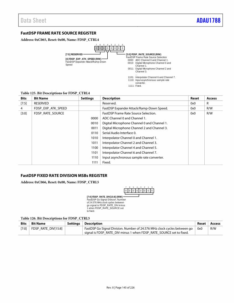
Data Sheet ADAU1788
Rev. 0 | Page 145 of 226
FastDSP FRAME RATE SOURCE REGISTER Address: 0xC065, Reset: 0x00, Name: FDSP_CTRL4
FastDSP Frame Rate Source Selection
1111: Fixed.
1110:converter.Input asynchronous sample rate
1101: Interpolator Channel 6 and Channel 7....
0011:Channel 3.Digital Microphone Channel 2 and
0010:Channel 1.Digital Microphone Channel 0 and
0000: ADC Channel 0 and Channel 1.FastDSP Expander Attack/Ramp-DownSpeed
0
01
02
03
04
05
06
07
0
[7:5] RESERVED [3:0] FDSP_RATE_SOURCE (R/W)
[4] FDSP_EXP_ATK_SPEED (R/W)
Table 125. Bit Descriptions for FDSP_CTRL4 Bits Bit Name Settings Description Reset Access [7:5] RESERVED Reserved. 0x0 R 4 FDSP_EXP_ATK_SPEED FastDSP Expander Attack/Ramp-Down Speed. 0x0 R/W [3:0] FDSP_RATE_SOURCE FastDSP Frame Rate Source Selection. 0x0 R/W 0000 ADC Channel 0 and Channel 1. 0010 Digital Microphone Channel 0 and Channel 1. 0011 Digital Microphone Channel 2 and Channel 3. 0110 Serial Audio Interface 0. 1010 Interpolator Channel 0 and Channel 1. 1011 Interpolator Channel 2 and Channel 3. 1100 Interpolator Channel 4 and Channel 5. 1101 Interpolator Channel 6 and Channel 7. 1110 Input asynchronous sample rate converter. 1111 Fixed.
FastDSP FIXED RATE DIVISION MSBs REGISTER Address: 0xC066, Reset: 0x00, Name: FDSP_CTRL5
FastDSP Go Signal Divis ion. Numberof 24.576 MHz clock cycles betweengo s ignal is FDSP_RATE_DIV minus1 when FDSP_RATE_SOURCE setto fixed.
0
01
02
03
04
05
06
07
0
[7:0] FDSP_RATE_DIV[15:8] (R/W)
Table 126. Bit Descriptions for FDSP_CTRL5 Bits Bit Name Settings Description Reset Access [7:0] FDSP_RATE_DIV[15:8] FastDSP Go Signal Division. Number of 24.576 MHz clock cycles between go
signal is FDSP_RATE_DIV minus 1 when FDSP_RATE_SOURCE set to fixed. 0x0 R/W

ADAU1788 Data Sheet
Rev. 0 | Page 146 of 226
FastDSP FIXED RATE DIVISION LSBs REGISTER Address: 0xC067, Reset: 0x7F, Name: FDSP_CTRL6
FastDSP Go Signal Divis ion. Numberof 24.576 MHz clock cycles betweengo s ignal is FDSP_RATE_DIV minus1 when FDSP_RATE_SOURCE setto fixed.
0
11
12
13
14
15
16
17
0
[7:0] FDSP_RATE_DIV[7:0] (R/W)
Table 127. Bit Descriptions for FDSP_CTRL6 Bits Bit Name Settings Description Reset Access [7:0] FDSP_RATE_DIV[7:0] FastDSP Go Signal Division. Number of 24.576 MHz clock cycles between go
signal is FDSP_RATE_DIV minus 1 when FDSP_RATE_SOURCE set to fixed. 0x7F R/W
FastDSP MODULO N COUNTER FOR LOWER RATE CONDITIONAL EXECUTION REGISTER Address: 0xC068, Reset: 0x00, Name: FDSP_CTRL7
FastDSP Modulo N Counter Resetfor Conditional Execution.
0
01
02
03
04
05
06
07
0
[7:6] RESERVED [5:0] FDSP_MOD_N (R/W)
Table 128. Bit Descriptions for FDSP_CTRL7 Bits Bit Name Settings Description Reset Access [7:6] RESERVED Reserved. 0x0 R [5:0] FDSP_MOD_N FastDSP Modulo N Counter Reset for Conditional Execution. 0x0 R/W

Data Sheet ADAU1788
Rev. 0 | Page 147 of 226
FastDSP GENERIC CONDITIONAL EXECUTION REGISTERS Address: 0xC069, Reset: 0x00, Name: FDSP_CTRL8
FastDSP Generic Register for ConditionalExecution
1: Conditional register is 1.0: Conditional register is 0.
FastDSP Generic Register for ConditionalExecution
1: Conditional register is 1.0: Conditional register is 0.
FastDSP Generic Register for ConditionalExecution
1: Conditional register is 1.0: Conditional register is 0.
FastDSP Generic Register for ConditionalExecution
1: Conditional register is 1.0: Conditional register is 0.
FastDSP Generic Register for ConditionalExecution
1: Conditional register is 1.0: Conditional register is 0.
FastDSP Generic Register for ConditionalExecution
1: Conditional register is 1.0: Conditional register is 0.
FastDSP Generic Register for ConditionalExecution
1: Conditional register is 1.0: Conditional register is 0.
FastDSP Generic Register for ConditionalExecution
1: Conditional register is 1.0: Conditional register is 0.
0
01
02
03
04
05
06
07
0
[7] FDSP_REG_COND7 (R/W) [0] FDSP_REG_COND0 (R/W)
[6] FDSP_REG_COND6 (R/W) [1] FDSP_REG_COND1 (R/W)
[5] FDSP_REG_COND5 (R/W) [2] FDSP_REG_COND2 (R/W)
[4] FDSP_REG_COND4 (R/W) [3] FDSP_REG_COND3 (R/W)
Table 129. Bit Descriptions for FDSP_CTRL8 Bits Bit Name Settings Description Reset Access 7 FDSP_REG_COND7 FastDSP Generic Register for Conditional Execution. The value of this register
can be used for conditional instruction execution in the FastDSP. 0x0 R/W
0 Conditional register is 0. 1 Conditional register is 1. 6 FDSP_REG_COND6 FastDSP Generic Register for Conditional Execution. The value of this register
can be used for conditional instruction execution in the FastDSP. 0x0 R/W
0 Conditional register is 0. 1 Conditional register is 1. 5 FDSP_REG_COND5 FastDSP Generic Register for Conditional Execution. The value of this register
can be used for conditional instruction execution in the FastDSP. 0x0 R/W
0 Conditional register is 0. 1 Conditional register is 1. 4 FDSP_REG_COND4 FastDSP Generic Register for Conditional Execution. The value of this register
can be used for conditional instruction execution in the FastDSP. 0x0 R/W
0 Conditional register is 0. 1 Conditional register is 1. 3 FDSP_REG_COND3 FastDSP Generic Register for Conditional Execution. The value of this register
can be used for conditional instruction execution in the FastDSP. 0x0 R/W
0 Conditional register is 0. 1 Conditional register is 1. 2 FDSP_REG_COND2 FastDSP Generic Register for Conditional Execution. The value of this register
can be used for conditional instruction execution in the FastDSP. 0x0 R/W
0 Conditional register is 0. 1 Conditional register is 1. 1 FDSP_REG_COND1 FastDSP Generic Register for Conditional Execution. The value of this register
can be used for conditional instruction execution in the FastDSP. 0x0 R/W
0 Conditional register is 0. 1 Conditional register is 1. 0 FDSP_REG_COND0 FastDSP Generic Register for Conditional Execution. The value of this register
can be used for conditional instruction execution in the FastDSP. 0x0 R/W
0 Conditional register is 0. 1 Conditional register is 1.
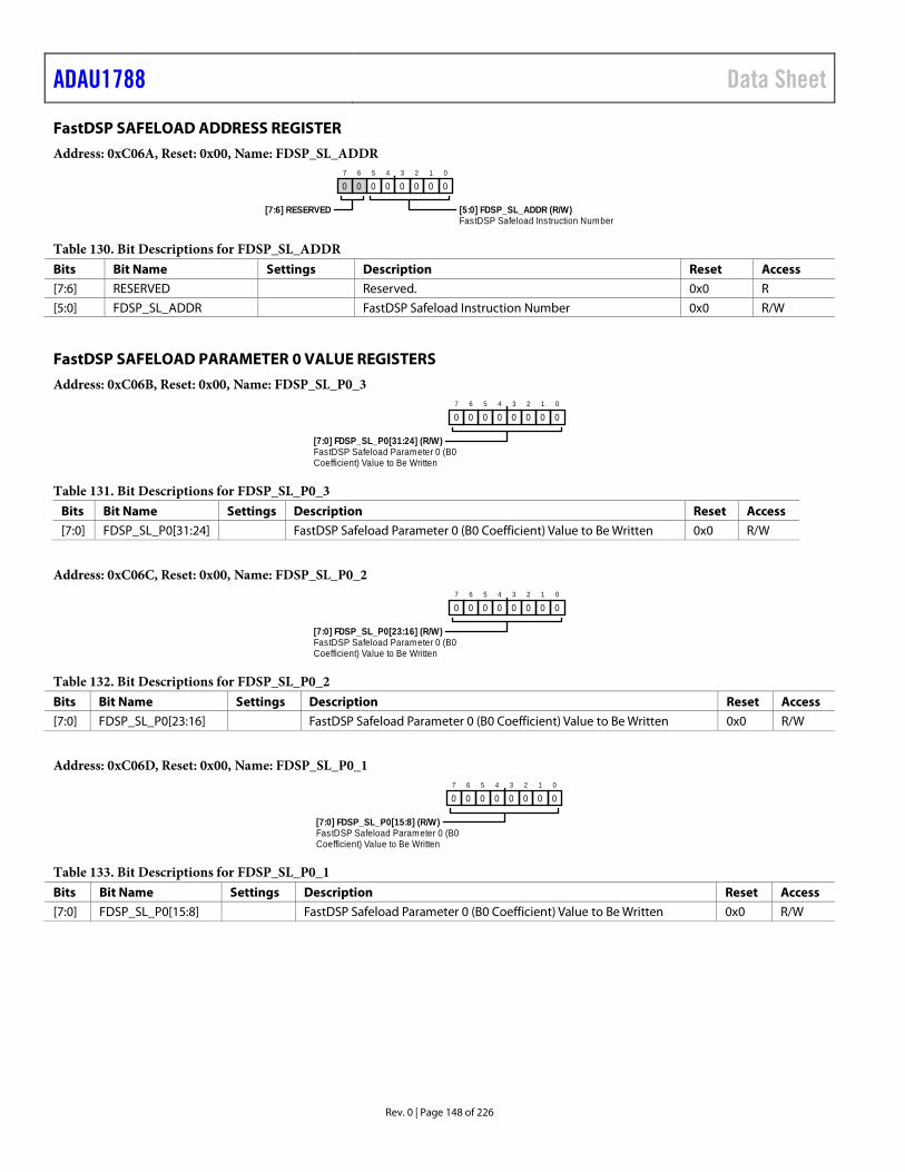
ADAU1788 Data Sheet
Rev. 0 | Page 148 of 226
FastDSP SAFELOAD ADDRESS REGISTER Address: 0xC06A, Reset: 0x00, Name: FDSP_SL_ADDR
FastDSP Safeload Instruction Number
0
01
02
03
04
05
06
07
0
[7:6] RESERVED [5:0] FDSP_SL_ADDR (R/W)
Table 130. Bit Descriptions for FDSP_SL_ADDR Bits Bit Name Settings Description Reset Access [7:6] RESERVED Reserved. 0x0 R [5:0] FDSP_SL_ADDR FastDSP Safeload Instruction Number 0x0 R/W
FastDSP SAFELOAD PARAMETER 0 VALUE REGISTERS Address: 0xC06B, Reset: 0x00, Name: FDSP_SL_P0_3
FastDSP Safeload Parameter 0 (B0Coefficient) Value to Be Written
0
01
02
03
04
05
06
07
0
[7:0] FDSP_SL_P0[31:24] (R/W)
Table 131. Bit Descriptions for FDSP_SL_P0_3 Bits Bit Name Settings Description Reset Access [7:0] FDSP_SL_P0[31:24] FastDSP Safeload Parameter 0 (B0 Coefficient) Value to Be Written 0x0 R/W
Address: 0xC06C, Reset: 0x00, Name: FDSP_SL_P0_2
FastDSP Safeload Parameter 0 (B0Coefficient) Value to Be Written
0
01
02
03
04
05
06
07
0
[7:0] FDSP_SL_P0[23:16] (R/W)
Table 132. Bit Descriptions for FDSP_SL_P0_2 Bits Bit Name Settings Description Reset Access [7:0] FDSP_SL_P0[23:16] FastDSP Safeload Parameter 0 (B0 Coefficient) Value to Be Written 0x0 R/W
Address: 0xC06D, Reset: 0x00, Name: FDSP_SL_P0_1
FastDSP Safeload Parameter 0 (B0Coefficient) Value to Be Written
0
01
02
03
04
05
06
07
0
[7:0] FDSP_SL_P0[15:8] (R/W)
Table 133. Bit Descriptions for FDSP_SL_P0_1 Bits Bit Name Settings Description Reset Access [7:0] FDSP_SL_P0[15:8] FastDSP Safeload Parameter 0 (B0 Coefficient) Value to Be Written 0x0 R/W

Data Sheet ADAU1788
Rev. 0 | Page 149 of 226
Address: 0xC06E, Reset: 0x00, Name: FDSP_SL_P0_0
FastDSP Safeload Parameter 0 (B0Coefficient) Value to Be Written
0
01
02
03
04
05
06
07
0
[7:0] FDSP_SL_P0[7:0] (R/W)
Table 134. Bit Descriptions for FDSP_SL_P0_0 Bits Bit Name Settings Description Reset Access [7:0] FDSP_SL_P0[7:0] FastDSP Safeload Parameter 0 (B0 Coefficient) Value to Be Written 0x0 R/W
FastDSP SAFELOAD PARAMETER 1 VALUE REGISTERS Address: 0xC06F, Reset: 0x00, Name: FDSP_SL_P1_3
FastDSP Safeload Parameter 1 (B1Coefficient) Value to Be Written
0
01
02
03
04
05
06
07
0
[7:0] FDSP_SL_P1[31:24] (R/W)
Table 135. Bit Descriptions for FDSP_SL_P1_3 Bits Bit Name Settings Description Reset Access [7:0] FDSP_SL_P1[31:24] FastDSP Safeload Parameter 1 (B1 Coefficient) Value to Be Written 0x0 R/W
Address: 0xC070, Reset: 0x00, Name: FDSP_SL_P1_2
FastDSP Safeload Parameter 1 (B1Coefficient) Value to Be Written
0
01
02
03
04
05
06
07
0
[7:0] FDSP_SL_P1[23:16] (R/W)
Table 136. Bit Descriptions for FDSP_SL_P1_2 Bits Bit Name Settings Description Reset Access [7:0] FDSP_SL_P1[23:16] FastDSP Safeload Parameter 1 (B1 Coefficient) Value to Be Written 0x0 R/W
Address: 0xC071, Reset: 0x00, Name: FDSP_SL_P1_1
FastDSP Safeload Parameter 1 (B1Coefficient) Value to Be Written
0
01
02
03
04
05
06
07
0
[7:0] FDSP_SL_P1[15:8] (R/W)
Table 137. Bit Descriptions for FDSP_SL_P1_1 Bits Bit Name Settings Description Reset Access [7:0] FDSP_SL_P1[15:8] FastDSP Safeload Parameter 1 (B1 Coefficient) Value to Be Written 0x0 R/W
Address: 0xC072, Reset: 0x00, Name: FDSP_SL_P1_0
FastDSP Safeload Parameter 1 (B1Coefficient) Value to Be Written
0
01
02
03
04
05
06
07
0
[7:0] FDSP_SL_P1[7:0] (R/W)
Table 138. Bit Descriptions for FDSP_SL_P1_0 Bits Bit Name Settings Description Reset Access [7:0] FDSP_SL_P1[7:0] FastDSP Safeload Parameter 1 (B1 Coefficient) Value to Be Written 0x0 R/W

ADAU1788 Data Sheet
Rev. 0 | Page 150 of 226
FastDSP SAFELOAD PARAMETER 2 VALUE REGISTERS Address: 0xC073, Reset: 0x00, Name: FDSP_SL_P2_3
FastDSP Safeload Parameter 2 (B2Coefficient) Value to Be Written
0
01
02
03
04
05
06
07
0
[7:0] FDSP_SL_P2[31:24] (R/W)
Table 139. Bit Descriptions for FDSP_SL_P2_3 Bits Bit Name Settings Description Reset Access [7:0] FDSP_SL_P2[31:24] FastDSP Safeload Parameter 2 (B2 Coefficient) Value to Be Written 0x0 R/W
Address: 0xC074, Reset: 0x00, Name: FDSP_SL_P2_2
FastDSP Safeload Parameter 2 (B2Coefficient) Value to Be Written
0
01
02
03
04
05
06
07
0
[7:0] FDSP_SL_P2[23:16] (R/W)
Table 140. Bit Descriptions for FDSP_SL_P2_2 Bits Bit Name Settings Description Reset Access [7:0] FDSP_SL_P2[23:16] FastDSP Safeload Parameter 2 (B2 Coefficient) Value to Be Written 0x0 R/W
Address: 0xC075, Reset: 0x00, Name: FDSP_SL_P2_1
FastDSP Safeload Parameter 2 (B2Coefficient) Value to Be Written
0
01
02
03
04
05
06
07
0
[7:0] FDSP_SL_P2[15:8] (R/W)
Table 141. Bit Descriptions for FDSP_SL_P2_1 Bits Bit Name Settings Description Reset Access [7:0] FDSP_SL_P2[15:8] FastDSP Safeload Parameter 2 (B2 Coefficient) Value to Be Written 0x0 R/W
Address: 0xC076, Reset: 0x00, Name: FDSP_SL_P2_0
FastDSP Safeload Parameter 2 (B2Coefficient) Value to Be Written
0
01
02
03
04
05
06
07
0
[7:0] FDSP_SL_P2[7:0] (R/W)
Table 142. Bit Descriptions for FDSP_SL_P2_0 Bits Bit Name Settings Description Reset Access [7:0] FDSP_SL_P2[7:0] FastDSP Safeload Parameter 2 (B2 Coefficient) Value to Be Written 0x0 R/W

Data Sheet ADAU1788
Rev. 0 | Page 151 of 226
FastDSP SAFELOAD PARAMETER 3 VALUE REGISTERS Address: 0xC077, Reset: 0x00, Name: FDSP_SL_P3_3
FastDSP Safeload Parameter 3 (A1Coefficient) Value to Be Written
0
01
02
03
04
05
06
07
0
[7:0] FDSP_SL_P3[31:24] (R/W)
Table 143. Bit Descriptions for FDSP_SL_P3_3 Bits Bit Name Settings Description Reset Access [7:0] FDSP_SL_P3[31:24] FastDSP Safeload Parameter 3 (A1 Coefficient) Value to Be Written 0x0 R/W
Address: 0xC078, Reset: 0x00, Name: FDSP_SL_P3_2
FastDSP Safeload Parameter 3 (A1Coefficient) Value to Be Written
0
01
02
03
04
05
06
07
0
[7:0] FDSP_SL_P3[23:16] (R/W)
Table 144. Bit Descriptions for FDSP_SL_P3_2 Bits Bit Name Settings Description Reset Access [7:0] FDSP_SL_P3[23:16] FastDSP Safeload Parameter 3 (A1 Coefficient) Value to Be Written 0x0 R/W
Address: 0xC079, Reset: 0x00, Name: FDSP_SL_P3_1
FastDSP Safeload Parameter 3 (A1Coefficient) Value to Be Written
0
01
02
03
04
05
06
07
0
[7:0] FDSP_SL_P3[15:8] (R/W)
Table 145. Bit Descriptions for FDSP_SL_P3_1 Bits Bit Name Settings Description Reset Access [7:0] FDSP_SL_P3[15:8] FastDSP Safeload Parameter 3 (A1 Coefficient) Value to Be Written 0x0 R/W
Address: 0xC07A, Reset: 0x00, Name: FDSP_SL_P3_0
FastDSP Safeload Parameter 3 (A1Coefficient) Value to Be Written
0
01
02
03
04
05
06
07
0
[7:0] FDSP_SL_P3[7:0] (R/W)
Table 146. Bit Descriptions for FDSP_SL_P3_0 Bits Bit Name Settings Description Reset Access [7:0] FDSP_SL_P3[7:0] FastDSP Safeload Parameter 3 (A1 Coefficient) Value to Be Written 0x0 R/W

ADAU1788 Data Sheet
Rev. 0 | Page 152 of 226
FastDSP SAFELOAD PARAMETER 4 VALUE REGISTERS Address: 0xC07B, Reset: 0x00, Name: FDSP_SL_P4_3
FastDSP Safeload Parameter 4 (A2Coefficient) Value to Be Written
0
01
02
03
04
05
06
07
0
[7:0] FDSP_SL_P4[31:24] (R/W)
Table 147. Bit Descriptions for FDSP_SL_P4_3 Bits Bit Name Settings Description Reset Access [7:0] FDSP_SL_P4[31:24] FastDSP Safeload Parameter 4 (A2 Coefficient) Value to Be Written 0x0 R/W
Address: 0xC07C, Reset: 0x00, Name: FDSP_SL_P4_2
FastDSP Safeload Parameter 4 (A2Coefficient) Value to Be Written
0
01
02
03
04
05
06
07
0
[7:0] FDSP_SL_P4[23:16] (R/W)
Table 148. Bit Descriptions for FDSP_SL_P4_2 Bits Bit Name Settings Description Reset Access [7:0] FDSP_SL_P4[23:16] FastDSP Safeload Parameter 4 (A2 Coefficient) Value to Be Written 0x0 R/W
Address: 0xC07D, Reset: 0x00, Name: FDSP_SL_P4_1
FastDSP Safeload Parameter 4 (A2Coefficient) Value to Be Written
0
01
02
03
04
05
06
07
0
[7:0] FDSP_SL_P4[15:8] (R/W)
Table 149. Bit Descriptions for FDSP_SL_P4_1 Bits Bit Name Settings Description Reset Access [7:0] FDSP_SL_P4[15:8] FastDSP Safeload Parameter 4 (A2 Coefficient) Value to Be Written 0x0 R/W
Address: 0xC07E, Reset: 0x00, Name: FDSP_SL_P4_0
FastDSP Safeload Parameter 4 (A2Coefficient) Value to Be Written
0
01
02
03
04
05
06
07
0
[7:0] FDSP_SL_P4[7:0] (R/W)
Table 150. Bit Descriptions for FDSP_SL_P4_0 Bits Bit Name Settings Description Reset Access [7:0] FDSP_SL_P4[7:0] FastDSP Safeload Parameter 4 (A2 Coefficient) Value to Be Written 0x0 R/W

Data Sheet ADAU1788
Rev. 0 | Page 153 of 226
FastDSP SAFELOAD UPDATE REGISTER Address: 0xC07F, Reset: 0x00, Name: FDSP_SL_UPDATE
FastDSP Safeload Update
1:
frame.parameters at the beginning of nextWriting of 1 causes update of safeload
0: No action.
0
01
02
03
04
05
06
07
0
[7:1] RESERVED [0] FDSP_SL_UPDATE (W)
Table 151. Bit Descriptions for FDSP_SL_UPDATE Bits Bit Name Settings Description Reset Access [7:1] RESERVED Reserved. 0x0 R 0 FDSP_SL_UPDATE FastDSP Safeload Update. Writing a 1 to this register writes the parameter
values in the FDSP_SL_Px registers to the addresses in the current bank associated with the instruction number in the FDSP_SL_ADDR register at the beginning of the next frame.
0x0 W
0 No action. 1 Writing of 1 causes update of safeload parameters at the beginning of next frame.
SigmaDSP FRAME RATE SOURCE SELECT REGISTER Address: 0xC080, Reset: 0x00, Name: SDSP_CTRL1
SigmaDSP Frame Rate Source
1111: Fixed rate determined by SDSP_RATE_DIV.
1110:converter.Input asynchronous sample rate
1101: Decimator Channel 6 and Channel 7....
0011:Channel 3.Digital Microphone Channel 2 and
0010:Channel 1.Digital Microphone Channel 0 and
0000: ADC Channel 0 and Channel 1.SigmaDSP Clock Speed Control.
1:
clock.operation using 49.152 MHz coreSigmaDSP high speed, high voltage
0:
clock.operation using 24.576 MHz coreSigmaDSP low speed, low voltage
0
01
02
03
04
05
06
07
0
[7:5] RESERVED [3:0] SDSP_RATE_SOURCE (R/W)
[4] SDSP_SPEED (R/W)
Table 152. Bit Descriptions for SDSP_CTRL1 Bits Bit Name Settings Description Reset Access [7:5] RESERVED Reserved. 0x0 R 4 SDSP_SPEED SigmaDSP Clock Speed Control. 0x0 R/W 0 SigmaDSP low speed, low voltage operation using 24.576 MHz core clock. 1 SigmaDSP high speed, high voltage operation using 49.152 MHz core clock. [3:0] SDSP_RATE_SOURCE SigmaDSP Frame Rate Source. 0x0 R/W 0000 ADC Channel 0 and Channel 1. 0010 Digital Microphone Channel 0 and Channel 1. 0011 Digital Microphone Channel 2 and Channel 3. 0110 Serial Audio Interface 0. 1010 Decimator Channel 0 and Channel 1. 1011 Decimator Channel 2 and Channel 3. 1100 Decimator Channel 4 and Channel 5. 1101 Decimator Channel 6 and Channel 7. 1110 Input asynchronous sample rate converter. 1111 Fixed rate determined by SDSP_RATE_DIV.

ADAU1788 Data Sheet
Rev. 0 | Page 154 of 226
SigmaDSP RUN REGISTER Address: 0xC081, Reset: 0x00, Name: SDSP_CTRL2
Allows SigmaDSP to run with thego s ignal
1:running.SigmaDSP has go s ignal and is
0:
if SDSP_EN = 1.running, but RAMs can be loadedSigmaDSP has no go s ignal. Not
0
01
02
03
04
05
06
07
0
[7:1] RESERVED [0] SDSP_RUN (R/W)
Table 153. Bit Descriptions for SDSP_CTRL2 Bits Bit Name Settings Description Reset Access [7:1] RESERVED Reserved. 0x0 R 0 SDSP_RUN Allows SigmaDSP to run with the go signal. 0x0 R/W 0 SigmaDSP has no go signal. Not running, but RAMs can be loaded if SDSP_EN = 1. 1 SigmaDSP has go signal and is running.
SigmaDSP WATCHDOG CONTROLS REGISTER Address: 0xC082, Reset: 0x00, Name: SDSP_CTRL3
SigmaDSP Watchdog Enable
1: SigmaDSP watchdog on.0: SigmaDSP watchdog off.SigmaDSP Watchdog Mute
1: SigmaDSP watchdog mute.0: SigmaDSP watchdog unmute.
0
01
02
03
04
05
06
07
0
[7:5] RESERVED [0] SDSP_WDOG_EN (R/W)
[4] SDSP_WDOG_MUTE (R/W)
[3:1] RESERVED
Table 154. Bit Descriptions for SDSP_CTRL3 Bits Bit Name Settings Description Reset Access [7:5] RESERVED Reserved. 0x0 R 4 SDSP_WDOG_MUTE SigmaDSP Watchdog Mute. 0x0 R/W 0 SigmaDSP watchdog unmute. 1 SigmaDSP watchdog mute. [3:1] RESERVED Reserved. 0x0 R 0 SDSP_WDOG_EN SigmaDSP Watchdog Enable. 0x0 R/W 0 SigmaDSP watchdog off. 1 SigmaDSP watchdog on.
SigmaDSP WATCHDOG VALUE REGISTERS Address: 0xC083, Reset: 0x00, Name: SDSP_CTRL4
SigmaDSP Watchdog Value
0
01
02
03
04
05
06
07
0
[7:0] SDSP_WDOG_VAL[23:16] (R/W)
Table 155. Bit Descriptions for SDSP_CTRL4 Bits Bit Name Settings Description Reset Access [7:0] SDSP_WDOG_VAL[23:16] SigmaDSP Watchdog Value 0x0 R/W

Data Sheet ADAU1788
Rev. 0 | Page 155 of 226
Address: 0xC084, Reset: 0x00, Name: SDSP_CTRL5
SigmaDSP Watchdog Value
0
01
02
03
04
05
06
07
0
[7:0] SDSP_WDOG_VAL[15:8] (R/W)
Table 156. Bit Descriptions for SDSP_CTRL5 Bits Bit Name Settings Description Reset Access [7:0] SDSP_WDOG_VAL[15:8] SigmaDSP Watchdog Value 0x0 R/W
Address: 0xC085, Reset: 0x00, Name: SDSP_CTRL6
SigmaDSP Watchdog Value
0
01
02
03
04
05
06
07
0
[7:0] SDSP_WDOG_VAL[7:0] (R/W)
Table 157. Bit Descriptions for SDSP_CTRL6 Bits Bit Name Settings Description Reset Access [7:0] SDSP_WDOG_VAL[7:0] SigmaDSP Watchdog Value 0x0 R/W
SigmaDSP MODULO DATA MEMORY START POSITION REGISTERS Address: 0xC086, Reset: 0x07, Name: SDSP_CTRL7
SigmaDSP Modulo Data MemoryStart Position
0
11
12
13
04
05
06
07
0
[7:4] RESERVED [3:0] SDSP_MOD_DATA_MEM[11:8] (R/W)
Table 158. Bit Descriptions for SDSP_CTRL7 Bits Bit Name Settings Description Reset Access [7:4] RESERVED Reserved 0x0 R [3:0] SDSP_MOD_DATA_MEM[11:8] SigmaDSP Modulo Data Memory Start Position 0x7 R/W
Address: 0xC087, Reset: 0xF4, Name: SDSP_CTRL8
SigmaDSP Modulo Data MemoryStart Position
0
01
02
13
04
15
16
17
1
[7:0] SDSP_MOD_DATA_MEM[7:0] (R/W)
Table 159. Bit Descriptions for SDSP_CTRL8 Bits Bit Name Settings Description Reset Access [7:0] SDSP_MOD_DATA_MEM[7:0] SigmaDSP Modulo Data Memory Start Position 0xF4 R/W

ADAU1788 Data Sheet
Rev. 0 | Page 156 of 226
SigmaDSP FIXED FRAME RATE DIVISOR REGISTERS Address: 0xC088, Reset: 0x07, Name: SDSP_CTRL9
SigmaDSP Go Signal Divis ion. Numberof 49.152 MHz clock cycles betweengo s ignal is SDSP_RATE_DIV plus1 when SDSP_RATE_SOURCE setto fixed.
0
11
12
13
04
05
06
07
0
[7:0] SDSP_RATE_DIV[15:8] (R/W)
Table 160. Bit Descriptions for SDSP_CTRL9 Bits Bit Name Settings Description Reset Access [7:0] SDSP_RATE_DIV[15:8] SigmaDSP Go Signal Division. Number of 49.152 MHz clock cycles between
go signal is SDSP_RATE_DIV plus 1 when SDSP_RATE_SOURCE set to fixed. 0x7 R/W
Address: 0xC089, Reset: 0xFF, Name: SDSP_CTRL10
SigmaDSP Go Signal Divis ion. Numberof 49.152 MHz clock cycles betweengo s ignal is SDSP_RATE_DIV plus1 when SDSP_RATE_SOURCE setto fixed.
0
11
12
13
14
15
16
17
1
[7:0] SDSP_RATE_DIV[7:0] (R/W)
Table 161. Bit Descriptions for SDSP_CTRL10 Bits Bit Name Settings Description Reset Access [7:0] SDSP_RATE_DIV[7:0] SigmaDSP Go Signal Division. Number of 49.152 MHz clock cycles between
go signal is SDSP_RATE_DIV plus 1 when SDSP_RATE_SOURCE set to fixed. 0xFF R/W
SigmaDSP SET INTERRUPTS REGISTER Address: 0xC08A, Reset: 0x00, Name: SDSP_CTRL11
SigmaDSP Trigger Interrupt 0
1: Writing of 1 triggers SigmaDSP interrupt.0: Writing of 0 has no effect.SigmaDSP Trigger Interrupt 3
1: Writing of 1 triggers SigmaDSP interrupt.0: Writing of 0 has no effect.
SigmaDSP Trigger Interrupt 1
1: Writing of 1 triggers SigmaDSP interrupt.0: Writing of 0 has no effect.SigmaDSP Trigger Interrupt 2
1: Writing of 1 triggers SigmaDSP interrupt.0: Writing of 0 has no effect.
0
01
02
03
04
05
06
07
0
[7:4] RESERVED [0] SDSP_INT0 (W)
[3] SDSP_INT3 (W)
[1] SDSP_INT1 (W)
[2] SDSP_INT2 (W)
Table 162. Bit Descriptions for SDSP_CTRL11 Bits Bit Name Settings Description Reset Access [7:4] RESERVED Reserved. 0x0 R 3 SDSP_INT3 SigmaDSP Trigger Interrupt 3. 0x0 W 0 Writing of 0 has no effect. 1 Writing of 1 triggers SigmaDSP interrupt. 2 SDSP_INT2 SigmaDSP Trigger Interrupt 2. 0x0 W 0 Writing of 0 has no effect. 1 Writing of 1 triggers SigmaDSP interrupt.

Data Sheet ADAU1788
Rev. 0 | Page 157 of 226
Bits Bit Name Settings Description Reset Access 1 SDSP_INT1 SigmaDSP Trigger Interrupt 1. 0x0 W 0 Writing of 0 has no effect. 1 Writing of 1 triggers SigmaDSP interrupt. 0 SDSP_INT0 SigmaDSP Trigger Interrupt 0. 0x0 W 0 Writing of 0 has no effect. 1 Writing of 1 triggers SigmaDSP interrupt.
MULTIPURPOSE PIN 0/PIN 1 MODE SELECT REGISTER Address: 0xC08B, Reset: 0x00, Name: MP_CTRL1
Multipurpose Pin 1 Mode Selection(BCLK_0).
0xA: PDM data output.0x9: PDM clock output.0x8: IRQ2 output.
...
0x4:bits .General-purpose output from GPIOx_OUT
0x3: General-purpose input.0x0: Normal operation.
Multipurpose Pin 0 Mode Selection(FSYNC_0).
0xA: PDM data output.0x9: PDM clock output.0x8: IRQ2 output.
...
0x4:bits .General-purpose output from GPIOx_OUT
0x3: General-purpose input.0x0: Normal operation.
0
01
02
03
04
05
06
07
0
[7:4] MP1_MODE (R/W) [3:0] MP0_MODE (R/W)
Table 163. Bit Descriptions for MP_CTRL1 Bits Bit Name Settings Description Reset Access [7:4] MP1_MODE Multipurpose Pin 1 Mode Selection (BCLK_0). 0x0 R/W 0x0 Normal operation. 0x3 General-purpose input. 0x4 General-purpose output from GPIOx_OUT bits. 0x5 General-purpose output from SigmaDSP. 0x6 Master clock output. 0x7 IRQ1 output. 0x8 IRQ2 output. 0x9 PDM clock output. 0xA PDM data output. [3:0] MP0_MODE Multipurpose Pin 0 Mode Selection (FSYNC_0). 0x0 R/W 0x0 Normal operation. 0x3 General-purpose input. 0x4 General-purpose output from GPIOx_OUT bits. 0x5 General-purpose output from SigmaDSP. 0x6 Master clock output. 0x7 IRQ1 output. 0x8 IRQ2 output. 0x9 PDM clock output. 0xA PDM data output.

ADAU1788 Data Sheet
Rev. 0 | Page 158 of 226
MULTIPURPOSE PIN 2/PIN 3 MODE SELECT REGISTER Address: 0xC08C, Reset: 0x00, Name: MP_CTRL2
Multipurpose Pin 3 Mode Selection(MP3).
0xA: PDM data output.0x9: PDM clock output.0x8: IRQ2 output.
...
0x4:bits .General-purpose output from GPIOx_OUT
0x3: General-purpose input.0x0: Normal operation.
Multipurpose Pin 2 Mode Selection(SDATAI_0).
0xA: PDM data output.0x9: PDM clock output.0x8: IRQ2 output.
...
0x4:bits .General-purpose output from GPIOx_OUT
0x3: General-purpose input.0x0: Normal operation.
0
01
02
03
04
05
06
07
0
[7:4] MP3_MODE (R/W) [3:0] MP2_MODE (R/W)
Table 164. Bit Descriptions for MP_CTRL2 Bits Bit Name Settings Description Reset Access [7:4] MP3_MODE Multipurpose Pin 3 Mode Selection (MP3). 0x0 R/W 0x0 Normal operation. 0x3 General-purpose input. 0x4 General-purpose output from GPIOx_OUT bits. 0x5 General-purpose output from SigmaDSP. 0x6 Master clock output. 0x7 IRQ1 output. 0x8 IRQ2 output. 0x9 PDM clock output. 0xA PDM data output. [3:0] MP2_MODE Multipurpose Pin 2 Mode Selection (SDATAI_0). 0x0 R/W 0x0 Normal operation. 0x3 General-purpose input. 0x4 General-purpose output from GPIOx_OUT bits. 0x5 General-purpose output from SigmaDSP. 0x6 Master clock output. 0x7 IRQ1 output. 0x8 IRQ2 output. 0x9 PDM clock output. 0xA PDM data output.

Data Sheet ADAU1788
Rev. 0 | Page 159 of 226
MULTIPURPOSE PIN 4/PIN 5 MODE SELECT REGISTER Address: 0xC08D, Reset: 0x00, Name: MP_CTRL3
Multipurpose Pin 5 Mode Selection(MP5).
0xA: PDM data output.0x9: PDM clock output.0x8: IRQ2 output.
...
0x4:bits .General-purpose output from GPIOx_OUT
0x3: General-purpose input.0x0: Normal operation.
Multipurpose Pin 4 Mode Selection(MP4).
0xA: PDM data output.0x9: PDM clock output.0x8: IRQ2 output.
...
0x4:bits .General-purpose output from GPIOx_OUT
0x3: General-purpose input.0x0: Normal operation.
0
01
02
03
04
05
06
07
0
[7:4] MP5_MODE (R/W) [3:0] MP4_MODE (R/W)
Table 165. Bit Descriptions for MP_CTRL3 Bits Bit Name Settings Description Reset Access [7:4] MP5_MODE Multipurpose Pin 5 Mode Selection (MP5). 0x0 R/W 0x0 Normal operation. 0x3 General-purpose input. 0x4 General-purpose output from GPIOx_OUT bits. 0x5 General-purpose output from SigmaDSP. 0x6 Master clock output. 0x7 IRQ1 output. 0x8 IRQ2 output. 0x9 PDM clock output. 0xA PDM data output. [3:0] MP4_MODE Multipurpose Pin 4 Mode Selection (MP4). 0x0 R/W 0x0 Normal operation. 0x3 General-purpose input. 0x4 General-purpose output from GPIOx_OUT bits. 0x5 General-purpose output from SigmaDSP. 0x6 Master clock output. 0x7 IRQ1 output. 0x8 IRQ2 output. 0x9 PDM clock output. 0xA PDM data output.

ADAU1788 Data Sheet
Rev. 0 | Page 160 of 226
MULTIPURPOSE PIN 6/PIN 7 MODE SELECT REGISTER Address: 0xC08E, Reset: 0x00, Name: MP_CTRL4
Multipurpose Pin 7 Mode Selection(DMIC_CLK0).
0xA: PDM data output.0x9: PDM clock output.0x8: IRQ2 output.
...
0x4:bits .General-purpose output from GPIOx_OUT
0x3: General-purpose input.0x0: Normal operation.
Multipurpose Pin 6 Mode Selection(MP6).
0xA: PDM data output.0x9: PDM clock output.0x8: IRQ2 output.
...
0x4:bits .General-purpose output from GPIOx_OUT
0x3: General-purpose input.0x0: Normal operation.
0
01
02
03
04
05
06
07
0
[7:4] MP7_MODE (R/W) [3:0] MP6_MODE (R/W)
Table 166. Bit Descriptions for MP_CTRL4 Bits Bit Name Settings Description Reset Access [7:4] MP7_MODE Multipurpose Pin 7 Mode Selection (DMIC_CLK0). 0x0 R/W 0x0 Normal operation. 0x3 General-purpose input. 0x4 General-purpose output from GPIOx_OUT bits. 0x5 General-purpose output from SigmaDSP. 0x6 Master clock output. 0x7 IRQ1 output. 0x8 IRQ2 output. 0x9 PDM clock output. 0xA PDM data output. [3:0] MP6_MODE Multipurpose Pin 6 Mode Selection (MP6). 0x0 R/W 0x0 Normal operation. 0x3 General-purpose input. 0x4 General-purpose output from GPIOx_OUT bits. 0x5 General-purpose output from SigmaDSP. 0x6 Master clock output. 0x7 IRQ1 output. 0x8 IRQ2 output. 0x9 PDM clock output. 0xA PDM data output.
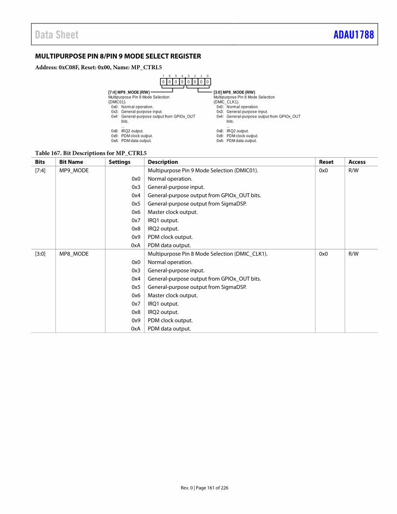
Data Sheet ADAU1788
Rev. 0 | Page 161 of 226
MULTIPURPOSE PIN 8/PIN 9 MODE SELECT REGISTER Address: 0xC08F, Reset: 0x00, Name: MP_CTRL5
Multipurpose Pin 9 Mode Selection(DMIC01).
0xA: PDM data output.0x9: PDM clock output.0x8: IRQ2 output.
...
0x4:bits .General-purpose output from GPIOx_OUT
0x3: General-purpose input.0x0: Normal operation.
Multipurpose Pin 8 Mode Selection(DMIC_CLK1).
0xA: PDM data output.0x9: PDM clock output.0x8: IRQ2 output.
...
0x4:bits .General-purpose output from GPIOx_OUT
0x3: General-purpose input.0x0: Normal operation.
0
01
02
03
04
05
06
07
0
[7:4] MP9_MODE (R/W) [3:0] MP8_MODE (R/W)
Table 167. Bit Descriptions for MP_CTRL5 Bits Bit Name Settings Description Reset Access [7:4] MP9_MODE Multipurpose Pin 9 Mode Selection (DMIC01). 0x0 R/W 0x0 Normal operation. 0x3 General-purpose input. 0x4 General-purpose output from GPIOx_OUT bits. 0x5 General-purpose output from SigmaDSP. 0x6 Master clock output. 0x7 IRQ1 output. 0x8 IRQ2 output. 0x9 PDM clock output. 0xA PDM data output. [3:0] MP8_MODE Multipurpose Pin 8 Mode Selection (DMIC_CLK1). 0x0 R/W 0x0 Normal operation. 0x3 General-purpose input. 0x4 General-purpose output from GPIOx_OUT bits. 0x5 General-purpose output from SigmaDSP. 0x6 Master clock output. 0x7 IRQ1 output. 0x8 IRQ2 output. 0x9 PDM clock output. 0xA PDM data output.

ADAU1788 Data Sheet
Rev. 0 | Page 162 of 226
MULTIPURPOSE PIN 10 MODE SELECT REGISTER Address: 0xC090, Reset: 0x00, Name: MP_CTRL6
Multipurpose Pin 10 Mode Selection(DMIC23).
0xA: PDM data output.0x9: PDM clock output.0x8: IRQ2 output.
...
0x4:bits .General-purpose output from GPIOx_OUT
0x3: General-purpose input.0x0: Normal operation.
0
01
02
03
04
05
06
07
0
[7:4] RESERVED [3:0] MP10_MODE (R/W)
Table 168. Bit Descriptions for MP_CTRL6 Bits Bit Name Settings Description Reset Access [7:4] RESERVED Reserved. 0x0 R/W [3:0] MP10_MODE Multipurpose Pin 10 Mode Selection (DMIC23). 0x0 R/W 0x0 Normal operation. 0x3 General-purpose input. 0x4 General-purpose output from GPIOx_OUT bits. 0x5 General-purpose output from SigmaDSP. 0x6 Master clock output. 0x7 IRQ1 output. 0x8 IRQ2 output. 0x9 PDM clock output. 0xA PDM data output.
GENERAL-PURPOSE INPUT DEBOUNCE CONTROL AND MASTER CLOCK OUTPUT RATE SELECTION REGISTER Address: 0xC091, Reset: 0x10, Name: MP_CTRL7
General-Purpose Input Debounce
110: GPIO input with debounce (20 ms).101: GPIO input with debounce (10 ms).100: GPIO input with debounce (5 ms).
11: GPIO input with debounce (0.9 ms).10: GPIO input with debounce (0.6 ms).
1: GPIO input with debounce (0.3 ms).0: GPIO input without debounce.Master Clock Output Rate Selection
111: Master clock output at 192 kHz.110: Master clock output at 384 kHz.101: Master clock output at 768 kHz.100: Master clock output at 1.536 MHz.
11: Master clock output at 3.072 MHz.10: Master clock output at 6.144 MHz.
1: Master clock output at 12.288 MHz.0: Master clock output at 24.576 MHz.
0
01
02
03
04
15
06
07
0
[7] RESERVED [2:0] GPI_DB (R/W)
[6:4] MCLKO_RATE (R/W)
[3] RESERVED
Table 169. Bit Descriptions for MP_CTRL7 Bits Bit Name Settings Description Reset Access 7 RESERVED Reserved. 0x0 R [6:4] MCLKO_RATE Master Clock Output Rate Selection. 0x1 R/W 0 Master clock output at 24.576 MHz. 1 Master clock output at 12.288 MHz. 10 Master clock output at 6.144 MHz. 11 Master clock output at 3.072 MHz. 100 Master clock output at 1.536 MHz. 101 Master clock output at 768 kHz. 110 Master clock output at 384 kHz. 111 Master clock output at 192 kHz. 3 RESERVED Reserved. 0x0 R

Data Sheet ADAU1788
Rev. 0 | Page 163 of 226
Bits Bit Name Settings Description Reset Access [2:0] GPI_DB General-Purpose Input Debounce. 0x0 R/W 0 GPIO input without debounce. 1 GPIO input with debounce (0.3 ms). 10 GPIO input with debounce (0.6 ms). 11 GPIO input with debounce (0.9 ms). 100 GPIO input with debounce (5 ms). 101 GPIO input with debounce (10 ms). 110 GPIO input with debounce (20 ms).
GENERAL-PURPOSE OUTPUTS CONTROL PIN 0 TO PIN 7 REGISTER Address: 0xC092, Reset: 0x00, Name: MP_CTRL8
GPIO7 Output Setting
1:output.MP7 pin set high when used as general-purpose
0:output.MP7 pin set low when used as general-purpose
GPIO0 Output Setting
1:output.MP0 pin set high when used as general-purpose
0:output.MP0 pin set low when used as general-purpose
GPIO6 Output Setting
1:output.MP6 pin set high when used as general-purpose
0:output.MP6 pin set low when used as general-purpose
GPIO1 Output Setting
1:output.MP1 pin set high when used as general-purpose
0:output.MP1 pin set low when used as general-purpose
GPIO5 Output Setting
1:output.MP5 pin set high when used as general-purpose
0:output.MP5 pin set low when used as general-purpose
GPIO2 Output Setting
1:output.MP2 pin set high when used as general-purpose
0:output.MP2 pin set low when used as general-purpose
GPIO4 Output Setting
1:output.MP4 pin set high when used as general-purpose
0:output.MP4 pin set low when used as general-purpose
GPIO3 Output Setting
1:output.MP3 pin set high when used as general-purpose
0:output.MP3 pin set low when used as general-purpose
0
01
02
03
04
05
06
07
0
[7] GPIO7_OUT (R/W) [0] GPIO0_OUT (R/W)
[6] GPIO6_OUT (R/W) [1] GPIO1_OUT (R/W)
[5] GPIO5_OUT (R/W) [2] GPIO2_OUT (R/W)
[4] GPIO4_OUT (R/W) [3] GPIO3_OUT (R/W)
Table 170. Bit Descriptions for MP_CTRL8 Bits Bit Name Settings Description Reset Access 7 GPIO7_OUT GPIO7 Output Setting. 0x0 R/W 0 MP7 pin set low when used as general-purpose output. 1 MP7 pin set high when used as general-purpose output. 6 GPIO6_OUT GPIO6 Output Setting. 0x0 R/W 0 MP6 pin set low when used as general-purpose output. 1 MP6 pin set high when used as general-purpose output. 5 GPIO5_OUT GPIO5 Output Setting. 0x0 R/W 0 MP5 pin set low when used as general-purpose output. 1 MP5 pin set high when used as general-purpose output. 4 GPIO4_OUT GPIO4 Output Setting. 0x0 R/W 0 MP4 pin set low when used as general-purpose output. 1 MP4 pin set high when used as general-purpose output. 3 GPIO3_OUT GPIO3 Output Setting. 0x0 R/W 0 MP3 pin set low when used as general-purpose output. 1 MP3 pin set high when used as general-purpose output. 2 GPIO2_OUT GPIO2 Output Setting. 0x0 R/W 0 MP2 pin set low when used as general-purpose output. 1 MP2 pin set high when used as general-purpose output.

ADAU1788 Data Sheet
Rev. 0 | Page 164 of 226
Bits Bit Name Settings Description Reset Access 1 GPIO1_OUT GPIO1 Output Setting. 0x0 R/W 0 MP1 pin set low when used as general-purpose output. 1 MP1 pin set high when used as general-purpose output. 0 GPIO0_OUT GPIO0 Output Setting. 0x0 R/W 0 MP0 pin set low when used as general-purpose output. 1 MP0 pin set high when used as general-purpose output.
GENERAL-PURPOSE OUTPUTS CONTROL PINS 8 TO PIN 10 REGISTER Address: 0xC093, Reset: 0x00, Name: MP_CTRL9
GPIO8 Output Setting
1:output.MP8 pin set high when used as general-purpose
0:output.MP8 pin set low when used as general-purposeGPIO10 Output Setting
1:general-purpose output.MP10 pin set high when used as
0:output.MP10 pin set low when used as general-purpose
GPIO9 Output Setting
1:output.MP9 pin set high when used as general-purpose
0:output.MP9 pin set low when used as general-purpose
0
01
02
03
04
05
06
07
0
[7:3] RESERVED [0] GPIO8_OUT (R/W)
[2] GPIO10_OUT (R/W)
[1] GPIO9_OUT (R/W)
Table 171. Bit Descriptions for MP_CTRL9 Bits Bit Name Settings Description Reset Access [7:3] RESERVED Reserved. 0x0 R 2 GPIO10_OUT GPIO10 Output Setting. 0x0 R/W 0 MP10 pin set low when used as general-purpose output. 1 MP10 pin set high when used as general-purpose output. 1 GPIO9_OUT GPIO9 Output Setting. 0x0 R/W 0 MP9 pin set low when used as general-purpose output. 1 MP9 pin set high when used as general-purpose output. 0 GPIO8_OUT GPIO8 Output Setting. 0x0 R/W 0 MP8 pin set low when used as general-purpose output. 1 MP8 pin set high when used as general-purpose output.

Data Sheet ADAU1788
Rev. 0 | Page 165 of 226
FSYNC_0 PIN CONTROLS REGISTER Address: 0xC094, Reset: 0x05, Name: FSYNC0_CTRL
FSYNC_0 Pin Drive Strength
11: 12 mA output drive.10: 8 mA output drive.
1: 4 mA output drive.0: 2 mA output drive.FSYNC_0 Pin Weak Pull-Up/Down
Selection
1: Weak pull-up when enabled.0: Weak pull-down when enabled.
FSYNC_0 Pin Slew Rate
1: Slow s lew rate.0: Fast s lew rate.FSYNC_0 Pin Weak Pull-Up/Down
Enable
1:FSYNC0_PULL_SEL bit.Weak pull-up or pull-down set by
0: No pull-up or pull-down.
0
11
02
13
04
05
06
07
0
[7:6] RESERVED [1:0] FSYNC0_DRIVE (R/W)
[5] FSYNC0_PULL_SEL (R/W)
[2] FSYNC0_SLEW (R/W)[4] FSYNC0_PULL_EN (R/W)
[3] RESERVED
Table 172. Bit Descriptions for FSYNC0_CTRL Bits Bit Name Settings Description Reset Access [7:6] RESERVED Reserved. 0x0 R 5 FSYNC0_PULL_SEL FSYNC_0 Pin Weak Pull-Up/Down Selection. 0x0 R/W 0 Weak pull-down when enabled. 1 Weak pull-up when enabled. 4 FSYNC0_PULL_EN FSYNC_0 Pin Weak Pull-Up/Down Enable. 0x0 R/W 0 No pull-up or pull-down. 1 Weak pull-up or pull-down set by FSYNC0_PULL_SEL bit. 3 RESERVED Reserved. 0x0 R 2 FSYNC0_SLEW FSYNC_0 Pin Slew Rate. Determines the slew rate of the pin when used as an
output. 0x1 R/W
0 Fast slew rate. 1 Slow slew rate. [1:0] FSYNC0_DRIVE FSYNC_0 Pin Drive Strength. Determines the drive strength of the pin when
used as an output. 0x1 R/W
0 2 mA output drive. 1 4 mA output drive. 10 8 mA output drive. 11 12 mA output drive.

ADAU1788 Data Sheet
Rev. 0 | Page 166 of 226
BCLK_0 PIN CONTROLS REGISTER Address: 0xC095, Reset: 0x05, Name: BCLK0_CTRL
BCLK_0 Pin Drive Strength
11: 12 mA output drive.10: 8 mA output drive.
1: 4 mA output drive.0: 2 mA output drive.BCLK_0 Pin Weak Pull-Up/Down
Selection
1: Weak pull-up when enabled.0: Weak pull-down when enabled.
BCLK_0 Pin Slew Rate
1: Slow s lew rate.0: Fast s lew rate.BCLK_0 Pin Weak Pull-Up/Down
Enable
1:BCLK0_PULL_SEL bit.Weak pull-up or pull-down set by
0: No pull-up or pull-down.
0
11
02
13
04
05
06
07
0
[7:6] RESERVED [1:0] BCLK0_DRIVE (R/W)
[5] BCLK0_PULL_SEL (R/W)
[2] BCLK0_SLEW (R/W)[4] BCLK0_PULL_EN (R/W)
[3] RESERVED
Table 173. Bit Descriptions for BCLK0_CTRL Bits Bit Name Settings Description Reset Access [7:6] RESERVED Reserved. 0x0 R 5 BCLK0_PULL_SEL BCLK_0 Pin Weak Pull-Up/Down Selection. 0x0 R/W 0 Weak pull-down when enabled. 1 Weak pull-up when enabled. 4 BCLK0_PULL_EN BCLK_0 Pin Weak Pull-Up/Down Enable. 0x0 R/W 0 No pull-up or pull-down. 1 Weak pull-up or pull-down set by BCLK0_PULL_SEL bit. 3 RESERVED Reserved. 0x0 R 2 BCLK0_SLEW BCLK_0 Pin Slew Rate. Determines the slew rate of the pin when used as an
output. 0x1 R/W
0 Fast slew rate. 1 Slow slew rate. [1:0] BCLK0_DRIVE BCLK_0 Pin Drive Strength. Determines the drive strength of the pin when used
as an output. 0x1 R/W
0 2 mA output drive. 1 4 mA output drive. 10 8 mA output drive. 11 12 mA output drive.
SDATAO_0 PIN CONTROL REGISTER Address: 0xC096, Reset: 0x04, Name: SDATAO0_CTRL
SDATAO_0 Pin Drive Strength
1: High drive strength.0: Normal drive strength.SDATAO_0 Pin Slew Rate
1: Slow s lew rate.0: Fast s lew rate.
0
01
02
13
04
05
06
07
0
[7:3] RESERVED [0] SDATAO0_DRIVE (R/W)
[2] SDATAO0_SLEW (R/W)
[1] RESERVED
Table 174. Bit Descriptions for SDATAO0_CTRL Bits Bit Name Settings Description Reset Access [7:3] RESERVED Reserved. 0x0 R 2 SDATAO0_SLEW SDATAO_0 Pin Slew Rate. Determines the slew rate of the pin when used as an
output. 0x1 R/W
0 Fast slew rate. 1 Slow slew rate

Data Sheet ADAU1788
Rev. 0 | Page 167 of 226
Bits Bit Name Settings Description Reset Access 1 RESERVED Reserved. 0x0 R 0 SDATAO0_DRIVE SDATAO_0 drive strength. 0x0 R/W 0 Normal drive strength. 1 High drive strength.
SDATAI_0 PIN CONTROLS REGISTER Address: 0xC097, Reset: 0x05, Name: SDATAI0_CTRL
SDATAI_0 Pin Drive Strength
11: 12 mA output drive.10: 8 mA output drive.
1: 4 mA output drive.0: 2 mA output drive.SDATAI_0 Pin Weak Pull-Up/Down
Selection
1: Weak pull-up when enabled.0: Weak pull-down when enabled.
SDATAI_0 Pin Slew Rate
1: Slow s lew rate.0: Fast s lew rate.SDATAI_0 Pin Weak Pull-Up/Down
Enable
1:SDATAI0_PULL_SEL bit.Weak pull-up or pull-down set by
0: No pull-up or pull-down.
0
11
02
13
04
05
06
07
0
[7:6] RESERVED [1:0] SDATAI0_DRIVE (R/W)
[5] SDATAI0_PULL_SEL (R/W)
[2] SDATAI0_SLEW (R/W)[4] SDATAI0_PULL_EN (R/W)
[3] RESERVED
Table 175. Bit Descriptions for SDATAI0_CTRL Bits Bit Name Settings Description Reset Access [7:6] RESERVED Reserved. 0x0 R 5 SDATAI0_PULL_SEL SDATAI_0 Pin Weak Pull-Up/Down Selection. 0x0 R/W 0 Weak pull-down when enabled. 1 Weak pull-up when enabled. 4 SDATAI0_PULL_EN SDATAI_0 Pin Weak Pull-Up/Down Enable. 0x0 R/W 0 No pull-up or pull-down. 1 Weak pull-up or pull-down set by SDATAI0_PULL_SEL bit. 3 RESERVED Reserved. 0x0 R 2 SDATAI0_SLEW SDATAI_0 Pin Slew Rate. Determines the slew rate of the pin when used as an
output. 0x1 R/W
0 Fast slew rate. 1 Slow slew rate. [1:0] SDATAI0_DRIVE SDATAI_0 Pin Drive Strength. Determines the drive strength of the pin when
used as an output. 0x1 R/W
0 2 mA output drive. 1 4 mA output drive. 10 8 mA output drive. 11 12 mA output drive.

ADAU1788 Data Sheet
Rev. 0 | Page 168 of 226
MP3 PIN CONTROLS REGISTER Address: 0xC098, Reset: 0x05, Name: MP3_CTRL
MP3 Pin Drive Strength
11: 12 mA output drive.10: 8 mA output drive.
1: 4 mA output drive.0: 2 mA output drive.MP3 Pin Weak Pull-Up/Down Selection
1: Weak pull-up when enabled.0: Weak pull-down when enabled.
MP3 Pin Slew Rate
1: Slow s lew rate.0: Fast s lew rate.
MP3 Pin Weak Pull-Up/Down Enable
1:MP3_PULL_SEL bit.Weak pull-up or pull-down set by
0: No pull-up or pull-down.
0
11
02
13
04
05
06
07
0
[7:6] RESERVED [1:0] MP3_DRIVE (R/W)
[5] MP3_PULL_SEL (R/W)
[2] MP3_SLEW (R/W)[4] MP3_PULL_EN (R/W)
[3] RESERVED
Table 176. Bit Descriptions for MP3_CTRL Bits Bit Name Settings Description Reset Access [7:6] RESERVED Reserved. 0x0 R 5 MP3_PULL_SEL MP3 Pin Weak Pull-Up/Down Selection. 0x0 R/W 0 Weak pull-down when enabled. 1 Weak pull-up when enabled. 4 MP3_PULL_EN MP3 Pin Weak Pull-Up/Down Enable. 0x0 R/W 0 No pull-up or pull-down. 1 Weak pull-up or pull-down set by MP3_PULL_SEL bit. 3 RESERVED Reserved. 0x0 R 2 MP3_SLEW MP3 Pin Slew Rate. Determines the slew rate of the pin when used as an output. 0x1 R/W 0 Fast slew rate. 1 Slow slew rate. [1:0] MP3_DRIVE MP3 Pin Drive Strength. Determines the drive strength of the pin when used as an
output. 0x1 R/W
0 2 mA output drive. 1 4 mA output drive. 10 8 mA output drive. 11 12 mA output drive.

Data Sheet ADAU1788
Rev. 0 | Page 169 of 226
MP4 PIN CONTROLS REGISTER Address: 0xC099, Reset: 0x05, Name: MP4_CTRL
MP4 Pin Drive Strength
11: 12 mA output drive.10: 8 mA output drive.
1: 4 mA output drive.0: 2 mA output drive.MP4 Pin Weak Pull-Up/Down Selection
1: Weak pull-up when enabled.0: Weak pull-down when enabled.
MP4 Pin Slew Rate
1: Slow s lew rate.0: Fast s lew rate.
MP4 Pin Weak Pull-Up/Down Enable
1:MP4_PULL_SEL bit.Weak pull-up or pull-down set by
0: No pull-up or pull-down.
0
11
02
13
04
05
06
07
0
[7:6] RESERVED [1:0] MP4_DRIVE (R/W)
[5] MP4_PULL_SEL (R/W)
[2] MP4_SLEW (R/W)[4] MP4_PULL_EN (R/W)
[3] RESERVED
Table 177. Bit Descriptions for MP4_CTRL Bits Bit Name Settings Description Reset Access [7:6] RESERVED Reserved. 0x0 R 5 MP4_PULL_SEL MP4 Pin Weak Pull-Up/Down Selection. 0x0 R/W 0 Weak pull-down when enabled. 1 Weak pull-up when enabled. 4 MP4_PULL_EN MP4 Pin Weak Pull-Up/Down Enable. 0x0 R/W 0 No pull-up or pull-down. 1 Weak pull-up or pull-down set by MP4_PULL_SEL bit. 3 RESERVED Reserved. 0x0 R 2 MP4_SLEW MP4 Pin Slew Rate. Determines the slew rate of the pin when used as an output. 0x1 R/W 0 Fast slew rate. 1 Slow slew rate. [1:0] MP4_DRIVE MP4 Pin Drive Strength. Determines the drive strength of the pin when used as an
output. 0x1 R/W
0 2 mA output drive. 1 4 mA output drive. 10 8 mA output drive. 11 12 mA output drive.
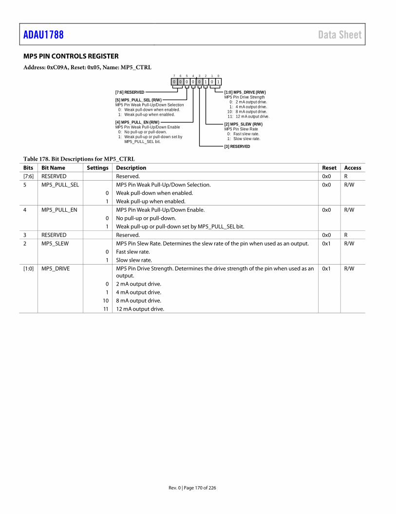
ADAU1788 Data Sheet
Rev. 0 | Page 170 of 226
MP5 PIN CONTROLS REGISTER Address: 0xC09A, Reset: 0x05, Name: MP5_CTRL
MP5 Pin Drive Strength
11: 12 mA output drive.10: 8 mA output drive.
1: 4 mA output drive.0: 2 mA output drive.MP5 Pin Weak Pull-Up/Down Selection
1: Weak pull-up when enabled.0: Weak pull-down when enabled.
MP5 Pin Slew Rate
1: Slow s lew rate.0: Fast s lew rate.
MP5 Pin Weak Pull-Up/Down Enable
1:MP5_PULL_SEL bit.Weak pull-up or pull-down set by
0: No pull-up or pull-down.
0
11
02
13
04
05
06
07
0
[7:6] RESERVED [1:0] MP5_DRIVE (R/W)
[5] MP5_PULL_SEL (R/W)
[2] MP5_SLEW (R/W)[4] MP5_PULL_EN (R/W)
[3] RESERVED
Table 178. Bit Descriptions for MP5_CTRL Bits Bit Name Settings Description Reset Access [7:6] RESERVED Reserved. 0x0 R 5 MP5_PULL_SEL MP5 Pin Weak Pull-Up/Down Selection. 0x0 R/W 0 Weak pull-down when enabled. 1 Weak pull-up when enabled. 4 MP5_PULL_EN MP5 Pin Weak Pull-Up/Down Enable. 0x0 R/W 0 No pull-up or pull-down. 1 Weak pull-up or pull-down set by MP5_PULL_SEL bit. 3 RESERVED Reserved. 0x0 R 2 MP5_SLEW MP5 Pin Slew Rate. Determines the slew rate of the pin when used as an output. 0x1 R/W 0 Fast slew rate. 1 Slow slew rate. [1:0] MP5_DRIVE MP5 Pin Drive Strength. Determines the drive strength of the pin when used as an
output. 0x1 R/W
0 2 mA output drive. 1 4 mA output drive. 10 8 mA output drive. 11 12 mA output drive.
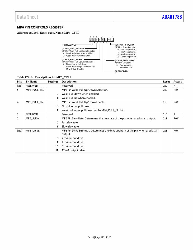
Data Sheet ADAU1788
Rev. 0 | Page 171 of 226
MP6 PIN CONTROLS REGISTER Address: 0xC09B, Reset: 0x05, Name: MP6_CTRL
MP6 Pin Drive Strength
11: 12 mA output drive.10: 8 mA output drive.
1: 4 mA output drive.0: 2 mA output drive.MP6 Pin Weak Pull-Up/Down Selection
1: Weak pull-up when enabled.0: Weak pull-down when enabled.
MP6 Pin Slew Rate
1: Slow s lew rate.0: Fast s lew rate.
MP6 Pin Weak Pull-Up/Down Enable
1:MP6_PULL_SEL bit.Weak pull-up or pull-down set by
0: No pull-up or pull-down.
0
11
02
13
04
05
06
07
0
[7:6] RESERVED [1:0] MP6_DRIVE (R/W)
[5] MP6_PULL_SEL (R/W)
[2] MP6_SLEW (R/W)[4] MP6_PULL_EN (R/W)
[3] RESERVED
Table 179. Bit Descriptions for MP6_CTRL Bits Bit Name Settings Description Reset Access [7:6] RESERVED Reserved. 0x0 R 5 MP6_PULL_SEL MP6 Pin Weak Pull-Up/Down Selection. 0x0 R/W 0 Weak pull-down when enabled. 1 Weak pull-up when enabled. 4 MP6_PULL_EN MP6 Pin Weak Pull-Up/Down Enable. 0x0 R/W 0 No pull-up or pull-down. 1 Weak pull-up or pull-down set by MP6_PULL_SEL bit. 3 RESERVED Reserved. 0x0 R 2 MP6_SLEW MP6 Pin Slew Rate. Determines the slew rate of the pin when used as an output. 0x1 R/W 0 Fast slew rate. 1 Slow slew rate. [1:0] MP6_DRIVE MP6 Pin Drive Strength. Determines the drive strength of the pin when used as an
output. 0x1 R/W
0 2 mA output drive. 1 4 mA output drive. 10 8 mA output drive. 11 12 mA output drive.

ADAU1788 Data Sheet
Rev. 0 | Page 172 of 226
DMIC_CLK0 PIN CONTROLS REGISTER Address: 0xC09C, Reset: 0x05, Name: DMIC_CLK0_CTRL
DMIC_CLK0 Pin Drive Strength
11: 12 mA output drive.10: 8 mA output drive.
1: 4 mA output drive.0: 2 mA output drive.DMIC_CLK0 Pin Weak Pull-Up/Down
Selection
1: Weak pull-up when enabled.0: Weak pull-down when enabled.
DMIC_CLK0 Pin Slew Rate
1: Slow s lew rate.0: Fast s lew rate.DMIC_CLK0 Pin Weak Pull-Up/Down
Enable
1:DMIC_CLK0_PULL_SEL bit.Weak pull-up or pull-down set by
0: No pull-up or pull-down.
0
11
02
13
04
05
06
07
0
[7:6] RESERVED [1:0] DMIC_CLK0_DRIVE (R/W)
[5] DMIC_CLK0_PULL_SEL (R/W)
[2] DMIC_CLK0_SLEW (R/W)[4] DMIC_CLK0_PULL_EN (R/W)
[3] RESERVED
Table 180. Bit Descriptions for DMIC_CLK0_CTRL Bits Bit Name Settings Description Reset Access [7:6] RESERVED Reserved. 0x0 R 5 DMIC_CLK0_PULL_SEL DMIC_CLK0 Pin Weak Pull-Up/Down Selection. 0x0 R/W 0 Weak pull-down when enabled. 1 Weak pull-up when enabled. 4 DMIC_CLK0_PULL_EN DMIC_CLK0 Pin Weak Pull-Up/Down Enable. 0x0 R/W 0 No pull-up or pull-down. 1 Weak pull-up or pull-down set by DMIC_CLK0_PULL_SEL bit. 3 RESERVED Reserved. 0x0 R 2 DMIC_CLK0_SLEW DMIC_CLK0 Pin Slew Rate. Determines the slew rate of the pin when used
as an output. 0x1 R/W
0 Fast slew rate. 1 Slow slew rate. [1:0] DMIC_CLK0_DRIVE DMIC_CLK0 Pin Drive Strength. Determines the drive strength of the pin
when used as an output. 0x1 R/W
0 2 mA output drive. 1 4 mA output drive. 10 8 mA output drive. 11 12 mA output drive.
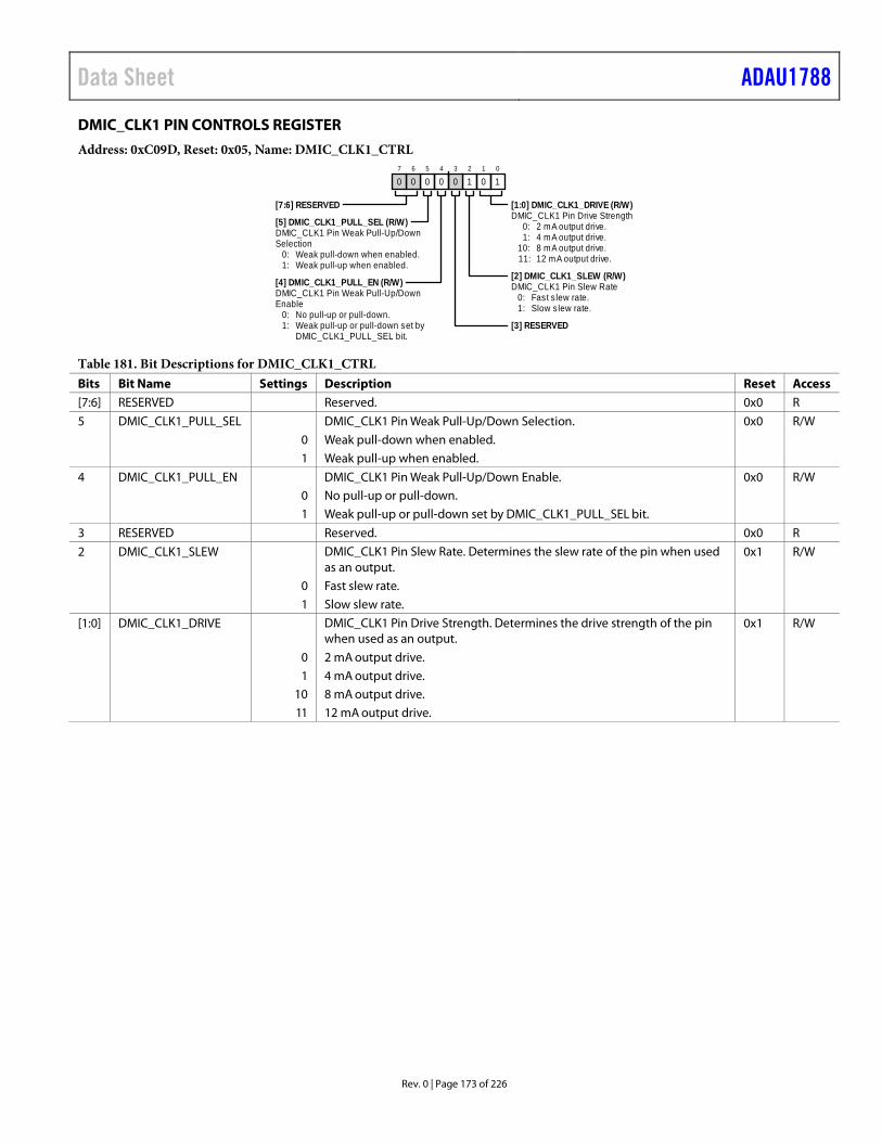
Data Sheet ADAU1788
Rev. 0 | Page 173 of 226
DMIC_CLK1 PIN CONTROLS REGISTER Address: 0xC09D, Reset: 0x05, Name: DMIC_CLK1_CTRL
DMIC_CLK1 Pin Drive Strength
11: 12 mA output drive.10: 8 mA output drive.
1: 4 mA output drive.0: 2 mA output drive.DMIC_CLK1 Pin Weak Pull-Up/Down
Selection
1: Weak pull-up when enabled.0: Weak pull-down when enabled.
DMIC_CLK1 Pin Slew Rate
1: Slow s lew rate.0: Fast s lew rate.DMIC_CLK1 Pin Weak Pull-Up/Down
Enable
1:DMIC_CLK1_PULL_SEL bit.Weak pull-up or pull-down set by
0: No pull-up or pull-down.
0
11
02
13
04
05
06
07
0
[7:6] RESERVED [1:0] DMIC_CLK1_DRIVE (R/W)
[5] DMIC_CLK1_PULL_SEL (R/W)
[2] DMIC_CLK1_SLEW (R/W)[4] DMIC_CLK1_PULL_EN (R/W)
[3] RESERVED
Table 181. Bit Descriptions for DMIC_CLK1_CTRL Bits Bit Name Settings Description Reset Access [7:6] RESERVED Reserved. 0x0 R 5 DMIC_CLK1_PULL_SEL DMIC_CLK1 Pin Weak Pull-Up/Down Selection. 0x0 R/W 0 Weak pull-down when enabled. 1 Weak pull-up when enabled. 4 DMIC_CLK1_PULL_EN DMIC_CLK1 Pin Weak Pull-Up/Down Enable. 0x0 R/W 0 No pull-up or pull-down. 1 Weak pull-up or pull-down set by DMIC_CLK1_PULL_SEL bit. 3 RESERVED Reserved. 0x0 R 2 DMIC_CLK1_SLEW DMIC_CLK1 Pin Slew Rate. Determines the slew rate of the pin when used
as an output. 0x1 R/W
0 Fast slew rate. 1 Slow slew rate. [1:0] DMIC_CLK1_DRIVE DMIC_CLK1 Pin Drive Strength. Determines the drive strength of the pin
when used as an output. 0x1 R/W
0 2 mA output drive. 1 4 mA output drive. 10 8 mA output drive. 11 12 mA output drive.
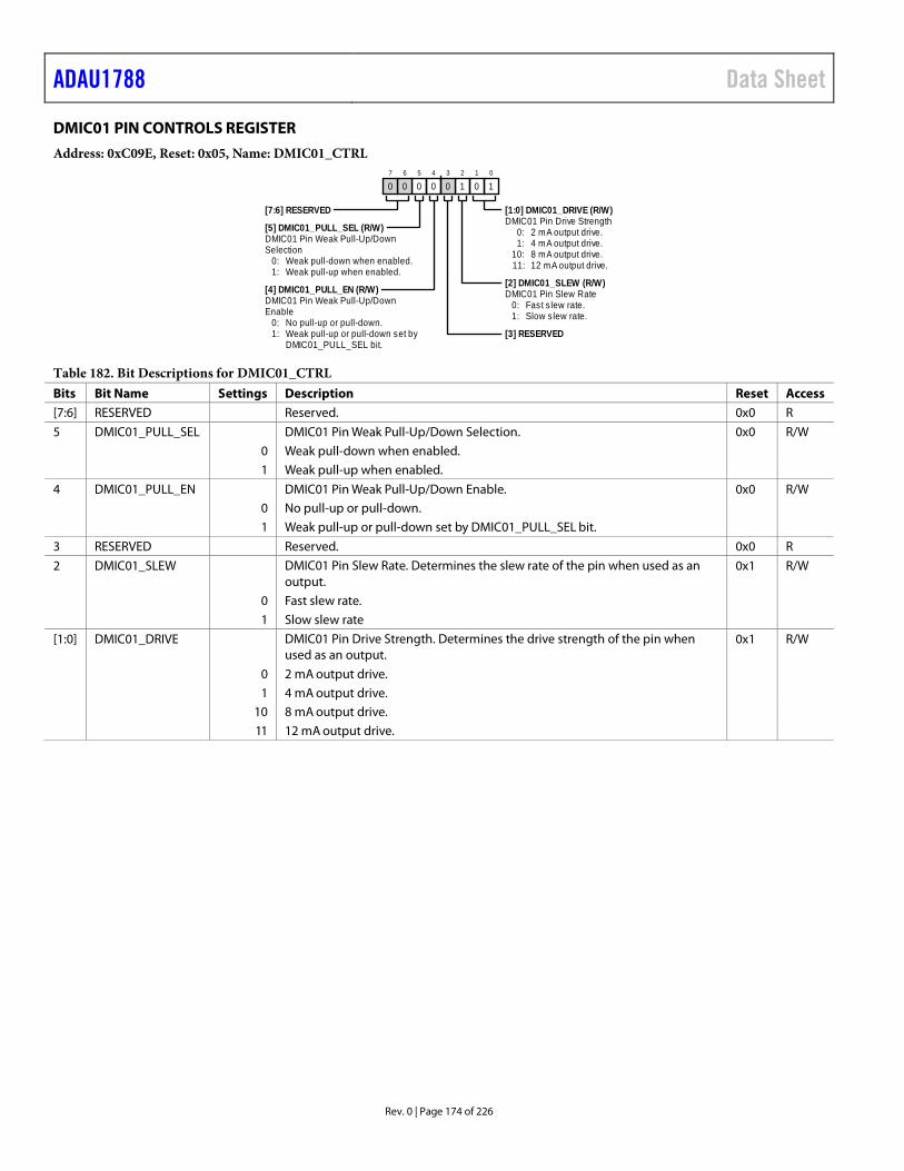
ADAU1788 Data Sheet
Rev. 0 | Page 174 of 226
DMIC01 PIN CONTROLS REGISTER Address: 0xC09E, Reset: 0x05, Name: DMIC01_CTRL
DMIC01 Pin Drive Strength
11: 12 mA output drive.10: 8 mA output drive.
1: 4 mA output drive.0: 2 mA output drive.DMIC01 Pin Weak Pull-Up/Down
Selection
1: Weak pull-up when enabled.0: Weak pull-down when enabled.
DMIC01 Pin Slew Rate
1: Slow s lew rate.0: Fast s lew rate.DMIC01 Pin Weak Pull-Up/Down
Enable
1:DMIC01_PULL_SEL bit.Weak pull-up or pull-down set by
0: No pull-up or pull-down.
0
11
02
13
04
05
06
07
0
[7:6] RESERVED [1:0] DMIC01_DRIVE (R/W)
[5] DMIC01_PULL_SEL (R/W)
[2] DMIC01_SLEW (R/W)[4] DMIC01_PULL_EN (R/W)
[3] RESERVED
Table 182. Bit Descriptions for DMIC01_CTRL Bits Bit Name Settings Description Reset Access [7:6] RESERVED Reserved. 0x0 R 5 DMIC01_PULL_SEL DMIC01 Pin Weak Pull-Up/Down Selection. 0x0 R/W 0 Weak pull-down when enabled. 1 Weak pull-up when enabled. 4 DMIC01_PULL_EN DMIC01 Pin Weak Pull-Up/Down Enable. 0x0 R/W 0 No pull-up or pull-down. 1 Weak pull-up or pull-down set by DMIC01_PULL_SEL bit. 3 RESERVED Reserved. 0x0 R 2 DMIC01_SLEW DMIC01 Pin Slew Rate. Determines the slew rate of the pin when used as an
output. 0x1 R/W
0 Fast slew rate. 1 Slow slew rate [1:0] DMIC01_DRIVE DMIC01 Pin Drive Strength. Determines the drive strength of the pin when
used as an output. 0x1 R/W
0 2 mA output drive. 1 4 mA output drive. 10 8 mA output drive. 11 12 mA output drive.

Data Sheet ADAU1788
Rev. 0 | Page 175 of 226
DMIC23 PIN CONTROLS REGISTER Address: 0xC09F, Reset: 0x05, Name: DMIC23_CTRL
DMIC23 Pin Drive Strength
11: 12 mA output drive.10: 8 mA output drive.
1: 4 mA output drive.0: 2 mA output drive.DMIC23 Pin Weak Pull-Up/Down
Selection
1: Weak pull-up when enabled.0: Weak pull-down when enabled.
DMIC23 Pin Slew Rate
1: Slow s lew rate.0: Fast s lew rate.DMIC23 Pin Weak Pull-Up/Down
Enable
1:DMIC23_PULL_SEL bit.Weak pull-up or pull-down set by
0: No pull-up or pull-down.
0
11
02
13
04
05
06
07
0
[7:6] RESERVED [1:0] DMIC23_DRIVE (R/W)
[5] DMIC23_PULL_SEL (R/W)
[2] DMIC23_SLEW (R/W)[4] DMIC23_PULL_EN (R/W)
[3] RESERVED
Table 183. Bit Descriptions for DMIC23_CTRL Bits Bit Name Settings Description Reset Access [7:6] RESERVED Reserved. 0x0 R 5 DMIC23_PULL_SEL DMIC23 Pin Weak Pull-Up/Down Selection. 0x0 R/W 0 Weak pull-down when enabled. 1 Weak pull-up when enabled. 4 DMIC23_PULL_EN DMIC23 Pin Weak Pull-Up/Down Enable. 0x0 R/W 0 No pull-up or pull-down. 1 Weak pull-up or pull-down set by DMIC23_PULL_SEL bit. 3 RESERVED Reserved. 0x0 R 2 DMIC23_SLEW DMIC23 Pin Slew Rate. Determines the slew rate of the pin when used as an
output. 0x1 R/W
0 Fast slew rate. 1 Slow slew rate [1:0] DMIC23_DRIVE DMIC23 Pin Drive Strength. Determines the drive strength of the pin when
used as an output. 0x1 R/W
0 2 mA output drive. 1 4 mA output drive. 10 8 mA output drive. 11 12 mA output drive.
SDA/MISO PIN CONTROLS REGISTER Address: 0xC0A0, Reset: 0x00, Name: I2C_SPI_CTRL
SDA/MISO Output Pin Drive Strength
1:C operation.2for fast mode plus I
20 mA drive strength. May be required0: 4 mA drive strength.SCL/SCLK Output Pin Drive Strength
1:C operation.2for fast mode plus I
20 mA drive strength. May be required0: 4 mA drive strength.
0
01
02
03
04
05
06
07
0
[7:2] RESERVED [0] SDA_MISO_DRIVE (R/W)
[1] SCL_SCLK_DRIVE (R/W)
Table 184. Bit Descriptions for I2C_SPI_CTRL Bits Bit Name Settings Description Reset Access [7:2] RESERVED Reserved. 0x0 R 1 SCL_SCLK_DRIVE SCL/SCLK Output Pin Drive Strength. 0x0 R/W 0 4 mA drive strength. 1 20 mA drive strength. May be required for fast mode plus I2C operation.

ADAU1788 Data Sheet
Rev. 0 | Page 176 of 226
Bits Bit Name Settings Description Reset Access 0 SDA_MISO_DRIVE SDA/MISO Output Pin Drive Strength. 0x0 R/W 0 4 mA drive strength. 1 20 mA drive strength. May be required for fast mode plus I2C operation.
IRQ SIGNALING AND CLEARING REGISTER Address: 0xC0A1, Reset: 0x00, Name: IRQ_CTRL1
Write Once to Clear IRQ1
1: Write once to clear IRQ1.0: Not applicable.IRQ2 Output Function Control
1: Active high interrupt s ignaling.0: Active low interrupt s ignaling.
Write Once to Clear IRQ2
1: Write once to clear IRQ2.0: Not applicable.IRQ1 Output Function Control
1:pin.Active high interrupt s ignaling on
0: Active low interrupt s ignaling on pin.
0
01
02
03
04
05
06
07
0
[7:6] RESERVED [0] IRQ1_CLEAR (R/W1T)
[5] IRQ2_FUNC (R/W)
[1] IRQ2_CLEAR (R/W1T)
[4] IRQ1_FUNC (R/W)
[3:2] RESERVED
Table 185. Bit Descriptions for IRQ_CTRL1 Bits Bit Name Settings Description Reset Access [7:6] RESERVED Reserved. 0x0 R 5 IRQ2_FUNC IRQ2 Output Function Control. 0x0 R/W 0 Active low interrupt signaling. 1 Active high interrupt signaling. 4 IRQ1_FUNC IRQ1 Output Function Control. 0x0 R/W 0 Active low interrupt signaling on pin. 1 Active high interrupt signaling on pin. [3:2] RESERVED Reserved. 0x0 R 1 IRQ2_CLEAR Write Once to Clear IRQ2. 0x0 R/W1T 0 Not applicable. 1 Write once to clear IRQ2. 0 IRQ1_CLEAR Write Once to Clear IRQ1. 0x0 R/W1T 0 Not applicable. 1 Write once to clear IRQ1.

Data Sheet ADAU1788
Rev. 0 | Page 177 of 226
IRQ1 MASKING REGISTERS Address: 0xC0A2, Reset: 0xF3, Name: IRQ1_MASK1
Mask DAC Channel 0 Clipping toIRQ1
1:IRQ.Event masked and does not cause
0: Event causes IRQ.Mask ADC Channel 1 Clipping toIRQ1
1:IRQ.Event masked and does not cause
0: Event causes IRQ.
Mask ADC Channel 0 Clipping toIRQ1
1:IRQ.Event masked and does not cause
0: Event causes IRQ.
0
11
12
03
04
15
16
17
1
[7:6] RESERVED [0] IRQ1_DAC0_CLIP_MASK (R/W)
[5] IRQ1_ADC1_CLIP_MASK (R/W)
[3:1] RESERVED
[4] IRQ1_ADC0_CLIP_MASK (R/W)
Table 186. Bit Descriptions for IRQ1_MASK1 Bits Bit Name Settings Description Reset Access [7:6] RESERVED Reserved. 0x3 R/W 5 IRQ1_ADC1_CLIP_MASK Mask ADC Channel 1 Clipping to IRQ1. 0x1 R/W 0 Event causes IRQ. 1 Event masked and does not cause IRQ. 4 IRQ1_ADC0_CLIP_MASK Mask ADC Channel 0 Clipping to IRQ1. 0x1 R/W 0 Event causes IRQ. 1 Event masked and does not cause IRQ. [3:1] RESERVED Reserved. 0x1 R 0 IRQ1_DAC0_CLIP_MASK Mask DAC Channel 0 Clipping to IRQ1. 0x1 R/W 0 Event causes IRQ. 1 Event masked and does not cause IRQ.

ADAU1788 Data Sheet
Rev. 0 | Page 178 of 226
Address: 0xC0A3, Reset: 0xFF, Name: IRQ1_MASK2
Mask Output ASRC Locked to UnlockedTransition to IRQ1
1:IRQ.Event masked and does not cause
0: Event causes IRQ.
Mask PLL Unlocked to Locked Transitionto IRQ1
1:IRQ.Event masked and does not cause
0: Event causes IRQ.
Mask Output ASRC Unlocked to LockedTransition to IRQ1
1:IRQ.Event masked and does not cause
0: Event causes IRQ.
Mask PLL Locked to Unlocked Transitionto IRQ1
1:IRQ.Event masked and does not cause
0: Event causes IRQ.
Mask Input ASRC Locked to UnlockedTransition to IRQ1
1:IRQ.Event masked and does not cause
0: Event causes IRQ.
Mask AVDD Undervoltage Warningto IRQ1
1:IRQ.Event masked and does not cause
0: Event causes IRQ.
Mask Input ASRC Unlocked to LockedTransition to IRQ1
1:IRQ.Event masked and does not cause
0: Event causes IRQ.
Mask Parameter Ramp CompleteTransition to IRQ1
1:IRQ.Event masked and does not cause
0: Event causes IRQ.
0
11
12
13
14
15
16
17
1
[7] IRQ1_ASRCO_UNLOCKED_MASK (R/W) [0] IRQ1_PLL_LOCKED_MASK (R/W)
[6] IRQ1_ASRCO_LOCKED_MASK (R/W) [1] IRQ1_PLL_UNLOCKED_MASK (R/W)
[5] IRQ1_ASRCI_UNLOCKED_MASK (R/W) [2] IRQ1_AVDD_UVW_MASK (R/W)
[4] IRQ1_ASRCI_LOCKED_MASK (R/W) [3] IRQ1_PRAMP_MASK (R/W)
Table 187. Bit Descriptions for IRQ1_MASK2 Bits Bit Name Settings Description Reset Access 7 IRQ1_ASRCO_UNLOCKED_MASK Mask Output ASRC Locked to Unlocked Transition to IRQ1. 0x1 R/W 0 Event causes IRQ. 1 Event masked and does not cause IRQ. 6 IRQ1_ASRCO_LOCKED_MASK Mask Output ASRC Unlocked to Locked Transition to IRQ1. 0x1 R/W 0 Event causes IRQ. 1 Event masked and does not cause IRQ. 5 IRQ1_ASRCI_UNLOCKED_MASK Mask Input ASRC Locked to Unlocked Transition to IRQ1. 0x1 R/W 0 Event causes IRQ. 1 Event masked and does not cause IRQ. 4 IRQ1_ASRCI_LOCKED_MASK Mask Input ASRC Unlocked to Locked Transition to IRQ1. 0x1 R/W 0 Event causes IRQ. 1 Event masked and does not cause IRQ. 3 IRQ1_PRAMP_MASK Mask Parameter Ramp Complete Transition to IRQ1. 0x1 R/W 0 Event causes IRQ. 1 Event masked and does not cause IRQ. 2 IRQ1_AVDD_UVW_MASK Mask AVDD Undervoltage Warning to IRQ1. 0x1 R/W 0 Event causes IRQ. 1 Event masked and does not cause IRQ. 1 IRQ1_PLL_UNLOCKED_MASK Mask PLL Locked to Unlocked Transition to IRQ1. 0x1 R/W 0 Event causes IRQ. 1 Event masked and does not cause IRQ. 0 IRQ1_PLL_LOCKED_MASK Mask PLL Unlocked to Locked Transition to IRQ1. 0x1 R/W 0 Event causes IRQ. 1 Event masked and does not cause IRQ.

Data Sheet ADAU1788
Rev. 0 | Page 179 of 226
Address: 0xC0A4, Reset: 0x1F, Name: IRQ1_MASK3
Mask SigmaDSP Interrupt 0 to IRQ1
1:IRQ.Event masked and does not cause
0: Event causes IRQ.Mask Power Up Not Finished to CompletedTransition to IRQ1
1:IRQ.Event masked and does not cause
0: Event causes IRQ.
Mask SigmaDSP Interrupt 1 to IRQ1
1:IRQ.Event masked and does not cause
0: Event causes IRQ.
Mask SigmaDSP Interrupt 3 to IRQ1
1:IRQ.Event masked and does not cause
0: Event causes IRQ.
Mask SigmaDSP Interrupt 2 to IRQ1
1:IRQ.Event masked and does not cause
0: Event causes IRQ.
0
11
12
13
14
15
06
07
0
[7:5] RESERVED [0] IRQ1_SDSP0_MASK (R/W)
[4] IRQ1_POWER_UP_COMPLETE_MASK (R/W)
[1] IRQ1_SDSP1_MASK (R/W)
[3] IRQ1_SDSP3_MASK (R/W)
[2] IRQ1_SDSP2_MASK (R/W)
Table 188. Bit Descriptions for IRQ1_MASK3 Bits Bit Name Settings Description Reset Access [7:5] RESERVED Reserved. 0x0 R 4 IRQ1_POWER_UP_COMPLETE_MASK Mask Power Up Not Finished to Completed Transition to IRQ1. 0x1 R/W 0 Event causes IRQ. 1 Event masked and does not cause IRQ. 3 IRQ1_SDSP3_MASK Mask SigmaDSP Interrupt 3 to IRQ1. 0x1 R/W 0 Event causes IRQ. 1 Event masked and does not cause IRQ. 2 IRQ1_SDSP2_MASK Mask SigmaDSP Interrupt 2 to IRQ1. 0x1 R/W 0 Event causes IRQ. 1 Event masked and does not cause IRQ. 1 IRQ1_SDSP1_MASK Mask SigmaDSP Interrupt 1 to IRQ1. 0x1 R/W 0 Event causes IRQ. 1 Event masked and does not cause IRQ. 0 IRQ1_SDSP0_MASK Mask SigmaDSP Interrupt 0 to IRQ1. 0x1 R/W 0 Event causes IRQ. 1 Event masked and does not cause IRQ.

ADAU1788 Data Sheet
Rev. 0 | Page 180 of 226
IRQ2 MASKING REGISTERS Address: 0xC0A5, Reset: 0xF3, Name: IRQ2_MASK1
Mask DAC Channel 0 Clipping toIRQ2
1:IRQ.Event masked and does not cause
0: Event causes IRQ.Mask ADC Channel 1 Clipping toIRQ2
1:IRQ.Event masked and does not cause
0: Event causes IRQ.
Mask ADC Channel 0 Clipping toIRQ2
1:IRQ.Event masked and does not cause
0: Event causes IRQ.
0
11
12
03
04
15
16
17
1
[7:6] RESERVED [0] IRQ2_DAC0_CLIP_MASK (R/W)
[5] IRQ2_ADC1_CLIP_MASK (R/W)
[3:1] RESERVED
[4] IRQ2_ADC0_CLIP_MASK (R/W)
Table 189. Bit Descriptions for IRQ2_MASK1 Bits Bit Name Settings Description Reset Access [7:6] RESERVED Reserved. 0x3 R/W 5 IRQ2_ADC1_CLIP_MASK Mask ADC Channel 1 Clipping to IRQ2. 0x1 R/W 0 Event causes IRQ. 1 Event masked and does not cause IRQ. 4 IRQ2_ADC0_CLIP_MASK Mask ADC Channel 0 Clipping to IRQ2. 0x1 R/W 0 Event causes IRQ. 1 Event masked and does not cause IRQ. [3:1] RESERVED Reserved. 0x1 R 0 IRQ2_DAC0_CLIP_MASK Mask DAC Channel 0 Clipping to IRQ2. 0x1 R/W 0 Event causes IRQ. 1 Event masked and does not cause IRQ.

Data Sheet ADAU1788
Rev. 0 | Page 181 of 226
Address: 0xC0A6, Reset: 0xFF, Name: IRQ2_MASK2
Mask Output ASRC Locked to UnlockedTransition to IRQ2
1:IRQ.Event masked and does not cause
0: Event causes IRQ.
Mask PLL Unlocked to Locked Transitionto IRQ2
1:IRQ.Event masked and does not cause
0: Event causes IRQ.
Mask Output ASRC Unlocked to LockedTransition to IRQ2
1:IRQ.Event masked and does not cause
0: Event causes IRQ.
Mask PLL Locked to Unlocked Transitionto IRQ2
1:IRQ.Event masked and does not cause
0: Event causes IRQ.
Mask Input ASRC Locked to UnlockedTransition to IRQ2
1:IRQ.Event masked and does not cause
0: Event causes IRQ.
Mask AVDD Undervoltage Warningto IRQ2
1:IRQ.Event masked and does not cause
0: Event causes IRQ.
Mask Input ASRC Unlocked to LockedTransition to IRQ2
1:IRQ.Event masked and does not cause
0: Event causes IRQ.
Mask Parameter Ramp CompleteTransition to IRQ2
1:IRQ.Event masked and does not cause
0: Event causes IRQ.
0
11
12
13
14
15
16
17
1
[7] IRQ2_ASRCO_UNLOCKED_MASK (R/W) [0] IRQ2_PLL_LOCKED_MASK (R/W)
[6] IRQ2_ASRCO_LOCKED_MASK (R/W) [1] IRQ2_PLL_UNLOCKED_MASK (R/W)
[5] IRQ2_ASRCI_UNLOCKED_MASK (R/W) [2] IRQ2_AVDD_UVW_MASK (R/W)
[4] IRQ2_ASRCI_LOCKED_MASK (R/W) [3] IRQ2_PRAMP_MASK (R/W)
Table 190. Bit Descriptions for IRQ2_MASK2 Bits Bit Name Settings Description Reset Access 7 IRQ2_ASRCO_UNLOCKED_MASK Mask Output ASRC Locked to Unlocked Transition to IRQ2. 0x1 R/W 0 Event causes IRQ. 1 Event masked and does not cause IRQ. 6 IRQ2_ASRCO_LOCKED_MASK Mask Output ASRC Unlocked to Locked Transition to IRQ2. 0x1 R/W 0 Event causes IRQ. 1 Event masked and does not cause IRQ. 5 IRQ2_ASRCI_UNLOCKED_MASK Mask Input ASRC Locked to Unlocked Transition to IRQ2. 0x1 R/W 0 Event causes IRQ. 1 Event masked and does not cause IRQ. 4 IRQ2_ASRCI_LOCKED_MASK Mask Input ASRC Unlocked to Locked Transition to IRQ2. 0x1 R/W 0 Event causes IRQ. 1 Event masked and does not cause IRQ. 3 IRQ2_PRAMP_MASK Mask Parameter Ramp Complete Transition to IRQ2. 0x1 R/W 0 Event causes IRQ. 1 Event masked and does not cause IRQ. 2 IRQ2_AVDD_UVW_MASK Mask AVDD Undervoltage Warning to IRQ2. 0x1 R/W 0 Event causes IRQ. 1 Event masked and does not cause IRQ. 1 IRQ2_PLL_UNLOCKED_MASK Mask PLL Locked to Unlocked Transition to IRQ2. 0x1 R/W 0 Event causes IRQ. 1 Event masked and does not cause IRQ. 0 IRQ2_PLL_LOCKED_MASK Mask PLL Unlocked to Locked Transition to IRQ2. 0x1 R/W 0 Event causes IRQ. 1 Event masked and does not cause IRQ.

ADAU1788 Data Sheet
Rev. 0 | Page 182 of 226
Address: 0xC0A7, Reset: 0x1F, Name: IRQ2_MASK3
Mask SigmaDSP Interrupt 0 to IRQ2
1:IRQ.Event masked and does not cause
0: Event causes IRQ.Mask Power Up Not Finished to CompletedTransition to IRQ2
1:IRQ.Event masked and does not cause
0: Event causes IRQ.
Mask SigmaDSP Interrupt 1 to IRQ2
1:IRQ.Event masked and does not cause
0: Event causes IRQ.
Mask SigmaDSP Interrupt 3 to IRQ2
1:IRQ.Event masked and does not cause
0: Event causes IRQ.
Mask SigmaDSP Interrupt 2 to IRQ2
1:IRQ.Event masked and does not cause
0: Event causes IRQ.
0
11
12
13
14
15
06
07
0
[7:5] RESERVED [0] IRQ2_SDSP0_MASK (R/W)
[4] IRQ2_POWER_UP_COMPLETE_MASK (R/W)
[1] IRQ2_SDSP1_MASK (R/W)
[3] IRQ2_SDSP3_MASK (R/W)
[2] IRQ2_SDSP2_MASK (R/W)
Table 191. Bit Descriptions for IRQ2_MASK3 Bits Bit Name Settings Description Reset Access [7:5] RESERVED Reserved. 0x0 R 4 IRQ2_POWER_UP_COMPLETE_MASK Mask Power Up Not Finished to Completed Transition to IRQ2. 0x1 R/W 0 Event causes IRQ. 1 Event masked and does not cause IRQ. 3 IRQ2_SDSP3_MASK Mask SigmaDSP Interrupt 3 to IRQ2. 0x1 R/W 0 Event causes IRQ. 1 Event masked and does not cause IRQ. 2 IRQ2_SDSP2_MASK Mask SigmaDSP Interrupt 2 to IRQ2. 0x1 R/W 0 Event causes IRQ. 1 Event masked and does not cause IRQ. 1 IRQ2_SDSP1_MASK Mask SigmaDSP Interrupt 1 to IRQ2. 0x1 R/W 0 Event causes IRQ. 1 Event masked and does not cause IRQ. 0 IRQ2_SDSP0_MASK Mask SigmaDSP Interrupt 0 to IRQ2. 0x1 R/W 0 Event causes IRQ. 1 Event masked and does not cause IRQ.
CHIP RESETS REGISTER Address: 0xC0A8, Reset: 0x00, Name: RESETS
Software Reset of Entire IC.
1: Write 1 once to soft full reset.0: Not applicable.Software Reset Not Including Register
Settings
1: Write 1 once to soft reset.0: Not applicable.
0
01
02
03
04
05
06
07
0
[7:5] RESERVED [0] SOFT_FULL_RESET (W)
[4] SOFT_RESET (W)
[3:1] RESERVED
Table 192. Bit Descriptions for RESETS Bits Bit Name Settings Description Reset Access [7:5] RESERVED Reserved. 0x0 R 4 SOFT_RESET Software Reset Not Including Register Settings. 0x0 W 0 Not applicable. 1 Write 1 once to soft reset.

Data Sheet ADAU1788
Rev. 0 | Page 183 of 226
Bits Bit Name Settings Description Reset Access [3:1] RESERVED Reserved. 0x0 R 0 SOFT_FULL_RESET Software Reset of Entire IC. 0x0 W 0 Not applicable. 1 Write 1 once to soft full reset.
FastDSP CURRENT LAMBDA REGISTER Address: 0xC0A9, Reset: 0x3F, Name: READ_LAMBDA
FastDSP Bank Switch Ramp CurrentLambda Status
63: Bank switch parameter ramp is complete.
62:63/64 of full ramp.Bank switch parameter ramp is at...
1:2/64 of full ramp.Bank switch parameter ramp is at
0:1/64 of full ramp.Bank switch parameter ramp is at
0
11
12
13
14
15
16
07
0
[7:6] RESERVED [5:0] FDSP_CURRENT_LAMBDA (R)
Table 193. Bit Descriptions for READ_LAMBDA Bits Bit Name Settings Description Reset Access [7:6] RESERVED Reserved. 0x0 R [5:0] FDSP_CURRENT_LAMBDA FastDSP Bank Switch Ramp Current Lambda Status. Lambda is a 6-bit
value representing the point along the linear interpolation curve between two banks at which the bank ramp switch stops. Where A represents coefficient values in the source bank, and B represents coefficient values in the destination bank: 0 = ((63/64) × A + (1/64) × B), 1 = ((62/64) × A + (2/64) × B), … , 62 = ((1/64) × A + (63/64) × B), 63 = B (default). Lambda can be updated on the fly via the control interface. To complete a bank switch, a value of 63 (default setting) must be set. Actual current ramp point (FDSP_CURRENT_LAMBDA: 0 to 63) can be read via a status register. When this point reaches 63, the bank switch is complete, and the current parameters used match the current bank. Actual step size of linear interpolation is ~12-bits (4096 steps). Parameters in banks ramped between do not change during a bank switch.
0x3F R
0 Bank switch parameter ramp is at 1/64 of full ramp. 1 Bank switch parameter ramp is at 2/64 of full ramp. … … 62 Bank switch parameter ramp is at 63/64 of full ramp. 63 Bank switch parameter ramp is complete.

ADAU1788 Data Sheet
Rev. 0 | Page 184 of 226
CHIP STATUS 1 REGISTER Address: 0xC0AA, Reset: 0x00, Name: STATUS1
DAC Channel 0 Clip Detector
1: Clipping detected.0: Normal operation.ADC Channel 1 Clip Detector
1: Amplifier clipping detected.0: Normal operation.
ADC Channel 0 Clip Detector
1: Amplifier clipping detected.0: Normal operation.
0
01
02
03
04
05
06
07
0
[7:6] RESERVED [0] DAC0_CLIP (R)
[5] ADC1_CLIP (R)
[3:1] RESERVED
[4] ADC0_CLIP (R)
Table 194. Bit Descriptions for STATUS1 Bits Bit Name Settings Description Reset Access [7:6] RESERVED Reserved. 0x0 R 5 ADC1_CLIP ADC Channel 1 Clip Detector. 0x0 R 0 Normal operation. 1 Amplifier clipping detected. 4 ADC0_CLIP ADC Channel 0 Clip Detector. 0x0 R 0 Normal operation. 1 Amplifier clipping detected. [3:1] RESERVED Reserved. 0x0 R 0 DAC0_CLIP DAC Channel 0 Clip Detector. 0x0 R 0 Normal operation. 1 Clipping detected.
CHIP STATUS 2 REGISTER Address: 0xC0AB, Reset: 0x00, Name: STATUS2
Status of the Power Domain PowerUp Caused by POWER_EN=1
Reads the PLL Lock Status
1: PLL is locked.0: PLL is not locked.
Reads the Multichip SynchronizationLock Status AVDD Undervoltage Warning
1: Undervoltage on AVDD detected.0: Normal operation.
Input ASRCI Lock Status
1: ASRC currently locked.0: ASRC currently unlocked.
Reads the Serial Port 0 Lock Status
Output ASRCI Lock Status
1: ASRC currently locked.0: ASRC currently unlocked.
0
01
02
03
04
05
06
07
0
[7] POWER_UP_COMPLETE (R) [0] PLL_LOCK (R)
[6] SYNC_LOCK (R)[1] AVDD_UVW (R)
[5] RESERVED
[2] ASRCI_LOCK (R)[4] SPT0_LOCK (R)
[3] ASRCO_LOCK (R)
Table 195. Bit Descriptions for STATUS2 Bits Bit Name Settings Description Reset Access 7 POWER_UP_COMPLETE Status of the Power Domain Power Up Caused by POWER_EN = 1. 0x0 R 6 SYNC_LOCK Reads the Multichip Synchronization Lock Status. 0x0 R 5 RESERVED Reserved. 0x0 R 4 SPT0_LOCK Reads the Serial Port 0 Lock Status. 0x0 R 3 ASRCO_LOCK Output ASRCI Lock Status. 0x0 R 0 ASRC currently unlocked. 1 ASRC currently locked.

Data Sheet ADAU1788
Rev. 0 | Page 185 of 226
Bits Bit Name Settings Description Reset Access 2 ASRCI_LOCK Input ASRCI Lock Status. 0x0 R 0 ASRC currently unlocked. 1 ASRC currently locked. 1 AVDD_UVW AVDD Undervoltage Warning. 0x0 R 0 Normal operation. 1 Undervoltage on AVDD detected. 0 PLL_LOCK Reads the PLL Lock Status. 0x0 R 0 PLL is not locked. 1 PLL is locked.
GENERAL-PURPOSE INPUT READ 0 TO INPUT READ 7 REGISTER Address: 0xC0AC, Reset: 0x00, Name: GPI1
GPIO7 Input Reading
1: MP7 (set as GPIO 7) is high.0: MP7 (set as GPIO 7) is low.
GPIO0 Input Reading
1: MP0 (set as GPIO 0) is high.0: MP0 (set as GPIO 0) is low.
GPIO6 Input Reading
1: MP6 (set as GPIO 6) is high.0: MP6 (set as GPIO 6) is low.
GPIO1 Input Reading
1: MP1 (set as GPIO 1) is high.0: MP1 (set as GPIO 1) is low.
GPIO5 Input Reading
1: MP5 (set as GPIO 5) is high.0: MP5 (set as GPIO 5) is low.
GPIO2 Input Reading
1: MP2 (set as GPIO 2) is high.0: MP2 (set as GPIO 2) is low.
GPIO4 Input Reading
1: MP4 (set as GPIO 4) is high.0: MP4 (set as GPIO 4) is low.
GPIO3 Input Reading
1: MP3 (set as GPIO 3) is high.0: MP3 (set as GPIO 3) is low.
0
01
02
03
04
05
06
07
0
[7] GPIO7_IN (R) [0] GPIO0_IN (R)
[6] GPIO6_IN (R) [1] GPIO1_IN (R)
[5] GPIO5_IN (R) [2] GPIO2_IN (R)
[4] GPIO4_IN (R) [3] GPIO3_IN (R)
Table 196. Bit Descriptions for GPI1 Bits Bit Name Settings Description Reset Access 7 GPIO7_IN GPIO7 Input Reading. 0x0 R 0 MP7 (set as GPIO 7) is low. 1 MP7 (set as GPIO 7) is high. 6 GPIO6_IN GPIO6 Input Reading. 0x0 R 0 MP6 (set as GPIO 6) is low. 1 MP6 (set as GPIO 6) is high. 5 GPIO5_IN GPIO5 Input Reading. 0x0 R 0 MP5 (set as GPIO 5) is low. 1 MP5 (set as GPIO 5) is high. 4 GPIO4_IN GPIO4 Input Reading. 0x0 R 0 MP4 (set as GPIO 4) is low. 1 MP4 (set as GPIO 4) is high. 3 GPIO3_IN GPIO3 Input Reading. 0x0 R 0 MP3 (set as GPIO 3) is low. 1 MP3 (set as GPIO 3) is high. 2 GPIO2_IN GPIO2 Input Reading. 0x0 R 0 MP2 (set as GPIO 2) is low. 1 MP2 (set as GPIO 2) is high.

ADAU1788 Data Sheet
Rev. 0 | Page 186 of 226
Bits Bit Name Settings Description Reset Access 1 GPIO1_IN GPIO1 Input Reading. 0x0 R 0 MP1 (set as GPIO 1) is low. 1 MP1 (set as GPIO 1) is high. 0 GPIO0_IN GPIO0 Input Reading. 0x0 R 0 MP0 (set as GPIO 0) is low. 1 MP0 (set as GPIO 0) is high.
GENERAL-PURPOSE INPUT READ 8 TO INPUT READ 10 REGISTER Address: 0xC0AD, Reset: 0x00, Name: GPI2
GPIO8 Input Reading
1: MP8 (set as GPIO 8) is high.0: MP8 (set as GPIO 8) is low.GPIO10 Input Reading
1: MP10 (set as GPIO 10) is high.0: MP10 (set as GPIO10) is low.
GPIO9 Input Reading
1: MP9 (set as GPIO 9) is high.0: MP9 (set as GPIO 9) is low.
0
01
02
03
04
05
06
07
0
[7:3] RESERVED [0] GPIO8_IN (R)
[2] GPIO10_IN (R)
[1] GPIO9_IN (R)
Table 197. Bit Descriptions for GPI2 Bits Bit Name Settings Description Reset Access [7:3] RESERVED Reserved. 0x0 R 2 GPIO10_IN GPIO10 Input Reading. 0x0 R 0 MP10 (set as GPIO10) is low. 1 MP10 (set as GPIO 10) is high. 1 GPIO9_IN GPIO9 Input Reading. 0x0 R 0 MP9 (set as GPIO 9) is low. 1 MP9 (set as GPIO 9) is high. 0 GPIO8_IN GPIO8 Input Reading. 0x0 R 0 MP8 (set as GPIO 8) is low. 1 MP8 (set as GPIO 8) is high.
DSP STATUS REGISTER Address: 0xC0AE, Reset: 0x00, Name: DSP_STATUS
SigmaDSP Watchdog Error
1: Watchdog error.0: No watchdog error.
0
01
02
03
04
05
06
07
0
[7:1] RESERVED [0] SDSP_WDOG_ERROR (R)
Table 198. Bit Descriptions for DSP_STATUS Bits Bit Name Settings Description Reset Access [7:1] RESERVED Reserved. 0x0 R 0 SDSP_WDOG_ERROR SigmaDSP Watchdog Error. 0x0 R 0 No watchdog error. 1 Watchdog error.

Data Sheet ADAU1788
Rev. 0 | Page 187 of 226
IRQ1 STATUS 1 REGISTER Address: 0xC0AF, Reset: 0x00, Name: IRQ1_STATUS1
DAC Channel 0 Clipping Detected
1: Clipping detected.0: Interrupt not triggered.ADC Channel 1 Clipping Detected
1: Clipping detected.0: Interrupt not triggered.
ADC Channel 0 Clipping Detected
1: Clipping detected.0: Interrupt not triggered.
0
01
02
03
04
05
06
07
0
[7:6] RESERVED [0] IRQ1_DAC0_CLIP (R)
[5] IRQ1_ADC1_CLIP (R)
[3:1] RESERVED
[4] IRQ1_ADC0_CLIP (R)
Table 199. Bit Descriptions for IRQ1_STATUS1 Bits Bit Name Settings Description Reset Access [7:6] RESERVED Reserved. 0x0 R 5 IRQ1_ADC1_CLIP ADC Channel 1 Clipping Detected. 0x0 R 0 Interrupt not triggered. 1 Clipping detected. 4 IRQ1_ADC0_CLIP ADC Channel 0 Clipping Detected. 0x0 R 0 Interrupt not triggered. 1 Clipping detected. [3:1] RESERVED Reserved. 0x0 R 0 IRQ1_DAC0_CLIP DAC Channel 0 Clipping Detected. 0x0 R 0 Interrupt not triggered. 1 Clipping detected.

ADAU1788 Data Sheet
Rev. 0 | Page 188 of 226
IRQ1 STATUS 2 REGISTER Address: 0xC0B0, Reset: 0x00, Name: IRQ1_STATUS2
Output ASRC Locked to UnlockedTransition Detected
1: Unlocked to locked transition detected.
0:event.Interrupt not triggered by PLL lock
PLL Unlocked to Locked TransitionDetected
1:detected.PLL unlocked to locked transition
0:event.Interrupt not triggered by PLL lock
Output ASRC Unlocked to LockedTransition Detected
1: Unlocked to locked transition detected.
0:event.Interrupt not triggered by PLL lock
PLL Locked to Unlocked TransitionDetected
1:detected.PLL unlocked to locked transition
0:event.Interrupt not triggered by PLL lock
Input ASRC Locked to Unlocked TransitionDetected
1: Unlocked to locked transition detected.
0:event.Interrupt not triggered by PLL lock AVDD Undervoltage Warning Detected
1: AVDD undervoltage warning detected.0: Interrupt not triggered.
Input ASRC Unlocked to Locked TransitionDetected
1: Unlocked to locked transition detected.
0:event.Interrupt not triggered by PLL lock
Parameter Ramp Complete Interrupt
1: Interrupt triggered.0: Interrupt not triggered.
0
01
02
03
04
05
06
07
0
[7] IRQ1_ASRCO_UNLOCKED (R) [0] IRQ1_PLL_LOCKED (R)
[6] IRQ1_ASRCO_LOCKED (R)[1] IRQ1_PLL_UNLOCKED (R)
[5] IRQ1_ASRCI_UNLOCKED (R)
[2] IRQ1_AVDD_UVW (R)
[4] IRQ1_ASRCI_LOCKED (R) [3] IRQ1_PRAMP (R)
Table 200. Bit Descriptions for IRQ1_STATUS2 Bits Bit Name Settings Description Reset Access 7 IRQ1_ASRCO_UNLOCKED Output ASRC Locked to Unlocked Transition Detected. 0x0 R 0 Interrupt not triggered by PLL lock event. 1 Unlocked to locked transition detected. 6 IRQ1_ASRCO_LOCKED Output ASRC Unlocked to Locked Transition Detected. 0x0 R 0 Interrupt not triggered by PLL lock event. 1 Unlocked to locked transition detected. 5 IRQ1_ASRCI_UNLOCKED Input ASRC Locked to Unlocked Transition Detected. 0x0 R 0 Interrupt not triggered by PLL lock event. 1 Unlocked to locked transition detected. 4 IRQ1_ASRCI_LOCKED Input ASRC Unlocked to Locked Transition Detected. 0x0 R 0 Interrupt not triggered by PLL lock event. 1 Unlocked to locked transition detected. 3 IRQ1_PRAMP Parameter Ramp Complete Interrupt. 0x0 R 0 Interrupt not triggered. 1 Interrupt triggered. 2 IRQ1_AVDD_UVW AVDD Undervoltage Warning Detected. 0x0 R 0 Interrupt not triggered. 1 AVDD undervoltage warning detected. 1 IRQ1_PLL_UNLOCKED PLL Locked to Unlocked Transition Detected. 0x0 R 0 Interrupt not triggered by PLL lock event. 1 PLL unlocked to locked transition detected. 0 IRQ1_PLL_LOCKED PLL Unlocked to Locked Transition Detected. 0x0 R 0 Interrupt not triggered by PLL lock event. 1 PLL unlocked to locked transition detected.

Data Sheet ADAU1788
Rev. 0 | Page 189 of 226
IRQ1 STATUS 3 REGISTER Address: 0xC0B1, Reset: 0x00, Name: IRQ1_STATUS3
SigmaDSP Interrupt 0
1: Interrupt triggered.0: Interrupt not triggered.Power Up Not Finished to Completed
Transition Detected
1: Power-up complete transition detected.
0:complete event.Interrupt not triggered by power-up
SigmaDSP Interrupt 1
1: Interrupt triggered.0: Interrupt not triggered.
SigmaDSP Interrupt 3
1: Interrupt triggered.0: Interrupt not triggered. SigmaDSP Interrupt 2
1: Interrupt triggered.0: Interrupt not triggered.
0
01
02
03
04
05
06
07
0
[7:5] RESERVED [0] IRQ1_SDSP0 (R)
[4] IRQ1_POWER_UP_COMPLETE (R)
[1] IRQ1_SDSP1 (R)
[3] IRQ1_SDSP3 (R)[2] IRQ1_SDSP2 (R)
Table 201. Bit Descriptions for IRQ1_STATUS3 Bits Bit Name Settings Description Reset Access [7:5] RESERVED Reserved. 0x0 R 4 IRQ1_POWER_UP_COMPLETE Power Up Not Finished to Completed Transition Detected. 0x0 R 0 Interrupt not triggered by power-up complete event. 1 Power-up complete transition detected. 3 IRQ1_SDSP3 SigmaDSP Interrupt 3. 0x0 R 0 Interrupt not triggered. 1 Interrupt triggered. 2 IRQ1_SDSP2 SigmaDSP Interrupt 2. 0x0 R 0 Interrupt not triggered. 1 Interrupt triggered. 1 IRQ1_SDSP1 SigmaDSP Interrupt 1. 0x0 R 0 Interrupt not triggered. 1 Interrupt triggered. 0 IRQ1_SDSP0 SigmaDSP Interrupt 0. 0x0 R 0 Interrupt not triggered. 1 Interrupt triggered.

ADAU1788 Data Sheet
Rev. 0 | Page 190 of 226
IRQ2 STATUS 1 REGISTER Address: 0xC0B2, Reset: 0x00, Name: IRQ2_STATUS1
DAC Channel 0 Clipping Detected
1: Clipping detected.0: Interrupt not triggered.ADC Channel 1 Clipping Detected
1: Clipping detected.0: Interrupt not triggered.
ADC Channel 0 Clipping Detected
1: Clipping detected.0: Interrupt not triggered.
0
01
02
03
04
05
06
07
0
[7:6] RESERVED [0] IRQ2_DAC0_CLIP (R)
[5] IRQ2_ADC1_CLIP (R)
[3:1] RESERVED
[4] IRQ2_ADC0_CLIP (R)
Table 202. Bit Descriptions for IRQ2_STATUS1 Bits Bit Name Settings Description Reset Access [7:6] RESERVED Reserved. 0x0 R 5 IRQ2_ADC1_CLIP ADC Channel 1 Clipping Detected. 0x0 R 0 Interrupt not triggered. 1 Clipping detected. 4 IRQ2_ADC0_CLIP ADC Channel 0 Clipping Detected. 0x0 R 0 Interrupt not triggered. 1 Clipping detected. [3:1] RESERVED Reserved. 0x0 R 0 IRQ2_DAC0_CLIP DAC Channel 0 Clipping Detected. 0x0 R 0 Interrupt not triggered. 1 Clipping detected.

Data Sheet ADAU1788
Rev. 0 | Page 191 of 226
IRQ2 STATUS 2 REGISTER Address: 0xC0B3, Reset: 0x00, Name: IRQ2_STATUS2
Output ASRC Locked to UnlockedTransition Detected
1: Unlocked to locked transition detected.
0:event.Interrupt not triggered by PLL lock
PLL Unlocked to Locked TransitionDetected
1:detected.PLL unlocked to locked transition
0:event.Interrupt not triggered by PLL lock
Output ASRC Unlocked to LockedTransition Detected
1: Unlocked to locked transition detected.
0:event.Interrupt not triggered by PLL lock
PLL Locked to Unlocked TransitionDetected
1:detected.PLL unlocked to locked transition
0:event.Interrupt not triggered by PLL lock
Input ASRC Locked to Unlocked TransitionDetected
1: Unlocked to locked transition detected.
0:event.Interrupt not triggered by PLL lock AVDD Undervoltage Warning Detected
1: AVDD undervoltage warning detected.0: Interrupt not triggered.
Input ASRC Unlocked to Locked TransitionDetected
1: Unlocked to locked transition detected.
0:event.Interrupt not triggered by PLL lock
Parameter Ramp Complete Interrupt
1: Interrupt triggered.0: Interrupt not triggered.
0
01
02
03
04
05
06
07
0
[7] IRQ2_ASRCO_UNLOCKED (R) [0] IRQ2_PLL_LOCKED (R)
[6] IRQ2_ASRCO_LOCKED (R)[1] IRQ2_PLL_UNLOCKED (R)
[5] IRQ2_ASRCI_UNLOCKED (R)
[2] IRQ2_AVDD_UVW (R)
[4] IRQ2_ASRCI_LOCKED (R) [3] IRQ2_PRAMP (R)
Table 203. Bit Descriptions for IRQ2_STATUS2 Bits Bit Name Settings Description Reset Access 7 IRQ2_ASRCO_UNLOCKED Output ASRC Locked to Unlocked Transition Detected. 0x0 R 0 Interrupt not triggered by PLL lock event. 1 Unlocked to locked transition detected. 6 IRQ2_ASRCO_LOCKED Output ASRC Unlocked to Locked Transition Detected. 0x0 R 0 Interrupt not triggered by PLL lock event. 1 Unlocked to locked transition detected. 5 IRQ2_ASRCI_UNLOCKED Input ASRC Locked to Unlocked Transition Detected. 0x0 R 0 Interrupt not triggered by PLL lock event. 1 Unlocked to locked transition detected. 4 IRQ2_ASRCI_LOCKED Input ASRC Unlocked to Locked Transition Detected. 0x0 R 0 Interrupt not triggered by PLL lock event. 1 Unlocked to locked transition detected. 3 IRQ2_PRAMP Parameter Ramp Complete Interrupt. 0x0 R 0 Interrupt not triggered. 1 Interrupt triggered. 2 IRQ2_AVDD_UVW AVDD Undervoltage Warning Detected. 0x0 R 0 Interrupt not triggered. 1 AVDD undervoltage warning detected. 1 IRQ2_PLL_UNLOCKED PLL Locked to Unlocked Transition Detected. 0x0 R 0 Interrupt not triggered by PLL lock event. 1 PLL unlocked to locked transition detected. 0 IRQ2_PLL_LOCKED PLL Unlocked to Locked Transition Detected. 0x0 R 0 Interrupt not triggered by PLL lock event. 1 PLL unlocked to locked transition detected.

ADAU1788 Data Sheet
Rev. 0 | Page 192 of 226
IRQ2 STATUS 3 REGISTER Address: 0xC0B4, Reset: 0x00, Name: IRQ2_STATUS3
SigmaDSP Interrupt 0
1: Interrupt triggered.0: Interrupt not triggered.Power Up Not Finished to Completed
Transition Detected
1: Power-up complete transition detected.
0:complete event.Interrupt not triggered by power-up
SigmaDSP Interrupt 1
1: Interrupt triggered.0: Interrupt not triggered.
SigmaDSP Interrupt 3
1: Interrupt triggered.0: Interrupt not triggered. SigmaDSP Interrupt 2
1: Interrupt triggered.0: Interrupt not triggered.
0
01
02
03
04
05
06
07
0
[7:5] RESERVED [0] IRQ2_SDSP0 (R)
[4] IRQ2_POWER_UP_COMPLETE (R)
[1] IRQ2_SDSP1 (R)
[3] IRQ2_SDSP3 (R)[2] IRQ2_SDSP2 (R)
Table 204. Bit Descriptions for IRQ2_STATUS3 Bits Bit Name Settings Description Reset Access [7:5] RESERVED Reserved. 0x0 R 4 IRQ2_POWER_UP_COMPLETE Power Up Not Finished to Completed Transition Detected. 0x0 R 0 Interrupt not triggered by power-up complete event. 1 Power-up complete transition detected. 3 IRQ2_SDSP3 SigmaDSP Interrupt 3. 0x0 R 0 Interrupt not triggered. 1 Interrupt triggered. 2 IRQ2_SDSP2 SigmaDSP Interrupt 2. 0x0 R 0 Interrupt not triggered. 1 Interrupt triggered. 1 IRQ2_SDSP1 SigmaDSP Interrupt 1. 0x0 R 0 Interrupt not triggered. 1 Interrupt triggered. 0 IRQ2_SDSP0 SigmaDSP Interrupt 0. 0x0 R 0 Interrupt not triggered. 1 Interrupt triggered.

Data Sheet ADAU1788
Rev. 0 | Page 193 of 226
SERIAL PORT 0 CONTROL 1 REGISTER Address: 0xC0B5, Reset: 0x00, Name: SPT0_CTRL1
Serial Port, Selects Frame ClockMode
1:wide pulse.TDM. Frame clock is s ingle bit clock
0:S, left justified, or right justified).2(I
Stereo. 50% duty cycle frame clockSerial Port Output, Tris tate Enable
0: Tris tate disable.1: Tris tate enable.
Serial Port, Selects Data Delay fromFrame Clock Edge
100: Delay by 16.011: Delay by 12.010: Delay by 8.000: S mode, delay by 1.2Typical I001: Left justified, delay by 0.
Serial Port, Selects Slot Width
10: 24 BCLKs per s lot.01: 16 BCLKs per s lot.00: 32 BCLKs per s lot.
0
01
02
03
04
05
06
07
0
[7] RESERVED [0] SPT0_SAI_MODE (R/W)
[6] SPT0_TRI_STATE (R/W)
[3:1] SPT0_DATA_FORMAT (R/W)[5:4] SPT0_SLOT_WIDTH (R/W)
Table 205. Bit Descriptions for SPT0_CTRL1 Bits Bit Name Settings Description Reset Access 7 RESERVED Reserved. 0x0 R/W 6 SPT0_TRI_STATE Serial Port Output, Tristate Enable. 0x0 R/W 1 Tristate enable. 0 Tristate disable. [5:4] SPT0_SLOT_WIDTH Serial Port, Selects Slot Width. 0x0 R/W 00 32 BCLKs per slot. 01 16 BCLKs per slot. 10 24 BCLKs per slot. [3:1] SPT0_DATA_FORMAT Serial Port, Selects Data Delay from Frame Clock Edge. 0x0 R/W 001 Left justified, delay by 0. 000 Typical I2S mode, delay by 1. 010 Delay by 8. 011 Delay by 12. 100 Delay by 16. 0 SPT0_SAI_MODE Serial Port, Selects Frame Clock Mode. 0x0 R/W 0 Stereo. 50% duty cycle frame clock (I2S, left justified, or right justified). 1 TDM. Frame clock is single bit clock wide pulse.

ADAU1788 Data Sheet
Rev. 0 | Page 194 of 226
SERIAL PORT 0 CONTROL 2 REGISTER Address: 0xC0B6, Reset: 0x00, Name: SPT0_CTRL2
Serial Port, Selects Frame ClockPolarity
1: Inverted polarity.0: Normal polarity.
Serial Port, Selects BCLK Sourceand Rate
100: Generates BCLK at 24.576 MHz.011: Generates BCLK at 12.288 MHz.010: Generates BCLK at 6.144 MHz.001: Generates BCLK at 3.072 MHz.000: BCLK is from external source.
Serial Port, Selects Frame ClockSource and Rate
111: Generates frame clock with 768 kHz.110: Generates frame clock with 384 kHz.101: Generates frame clock with 24 kHz.100: Generates frame clock with 12 kHz.011: Generates frame clock with 192 kHz.010: Generates frame clock with 96 kHz.001: Generates frame clock with 48 kHz.000: Frame clock is from external source.
Serial Port, Selects BCLK Polarity
1: Captured on falling edge.0: Captured on ris ing edge.
0
01
02
03
04
05
06
07
0
[7] SPT0_LRCLK_POL (R/W) [2:0] SPT0_BCLK_SRC (R/W)
[6:4] SPT0_LRCLK_SRC (R/W)
[3] SPT0_BCLK_POL (R/W)
Table 206. Bit Descriptions for SPT0_CTRL2 Bits Bit Name Settings Description Reset Access 7 SPT0_LRCLK_POL Serial Port, Selects Frame Clock Polarity. 0x0 R/W 0 Normal polarity. 1 Inverted polarity. [6:4] SPT0_LRCLK_SRC Serial Port, Selects Frame Clock Source and Rate. 0x0 R/W 000 Frame clock is from external source. 001 Generates frame clock with 48 kHz. 010 Generates frame clock with 96 kHz. 011 Generates frame clock with 192 kHz. 100 Generates frame clock with 12 kHz. 101 Generates frame clock with 24 kHz. 110 Generates frame clock with 384 kHz. 111 Generates frame clock with 768 kHz. 3 SPT0_BCLK_POL Serial Port, Selects BCLK Polarity. 0x0 R/W 0 Captured on rising edge. 1 Captured on falling edge. [2:0] SPT0_BCLK_SRC Serial Port, Selects BCLK Source and Rate. 0x0 R/W 000 BCLK is from external source. 001 Generates BCLK at 3.072 MHz. 010 Generates BCLK at 6.144 MHz. 011 Generates BCLK at 12.288 MHz. 100 Generates BCLK at 24.576 MHz.
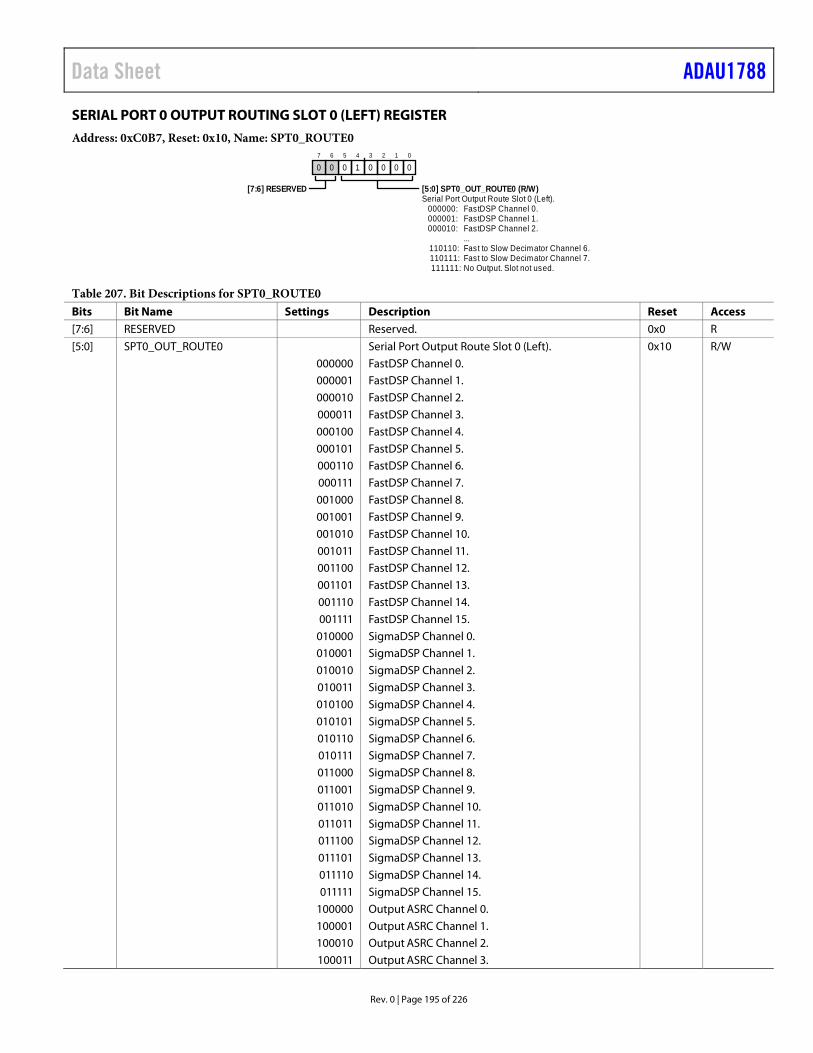
Data Sheet ADAU1788
Rev. 0 | Page 195 of 226
SERIAL PORT 0 OUTPUT ROUTING SLOT 0 (LEFT) REGISTER Address: 0xC0B7, Reset: 0x10, Name: SPT0_ROUTE0
Serial Port Output Route Slot 0 (Left).
111111: No Output. Slot not used.110111: Fast to Slow Decimator Channel 7.110110: Fast to Slow Decimator Channel 6.
...000010: FastDSP Channel 2.000001: FastDSP Channel 1.000000: FastDSP Channel 0.
0
01
02
03
04
15
06
07
0
[7:6] RESERVED [5:0] SPT0_OUT_ROUTE0 (R/W)
Table 207. Bit Descriptions for SPT0_ROUTE0 Bits Bit Name Settings Description Reset Access [7:6] RESERVED Reserved. 0x0 R [5:0] SPT0_OUT_ROUTE0 Serial Port Output Route Slot 0 (Left). 0x10 R/W 000000 FastDSP Channel 0. 000001 FastDSP Channel 1. 000010 FastDSP Channel 2. 000011 FastDSP Channel 3. 000100 FastDSP Channel 4. 000101 FastDSP Channel 5. 000110 FastDSP Channel 6. 000111 FastDSP Channel 7. 001000 FastDSP Channel 8. 001001 FastDSP Channel 9. 001010 FastDSP Channel 10. 001011 FastDSP Channel 11. 001100 FastDSP Channel 12. 001101 FastDSP Channel 13. 001110 FastDSP Channel 14. 001111 FastDSP Channel 15. 010000 SigmaDSP Channel 0. 010001 SigmaDSP Channel 1. 010010 SigmaDSP Channel 2. 010011 SigmaDSP Channel 3. 010100 SigmaDSP Channel 4. 010101 SigmaDSP Channel 5. 010110 SigmaDSP Channel 6. 010111 SigmaDSP Channel 7. 011000 SigmaDSP Channel 8. 011001 SigmaDSP Channel 9. 011010 SigmaDSP Channel 10. 011011 SigmaDSP Channel 11. 011100 SigmaDSP Channel 12. 011101 SigmaDSP Channel 13. 011110 SigmaDSP Channel 14. 011111 SigmaDSP Channel 15. 100000 Output ASRC Channel 0. 100001 Output ASRC Channel 1. 100010 Output ASRC Channel 2. 100011 Output ASRC Channel 3.

ADAU1788 Data Sheet
Rev. 0 | Page 196 of 226
Bits Bit Name Settings Description Reset Access 100100 ADC Channel 0. 100101 ADC Channel 1. 101000 Digital Microphone Channel 0. 101001 Digital Microphone Channel 1. 101010 Digital Microphone Channel 2. 101011 Digital Microphone Channel 3. 110000 Fast to Slow Decimator Channel 0. 110001 Fast to Slow Decimator Channel 1. 110010 Fast to Slow Decimator Channel 2. 110011 Fast to Slow Decimator Channel 3. 110100 Fast to Slow Decimator Channel 4. 110101 Fast to Slow Decimator Channel 5. 110110 Fast to Slow Decimator Channel 6. 110111 Fast to Slow Decimator Channel 7. 111111 No Output. Slot not used.
SERIAL PORT 0 OUTPUT ROUTING SLOT 1 (RIGHT) REGISTER Address: 0xC0B8, Reset: 0x11, Name: SPT0_ROUTE1
Serial Port Output Route Slot 1 (Right).
111111: No Output. Slot not used.110111: Fast to Slow Decimator Channel 7.110110: Fast to Slow Decimator Channel 6.
...000010: FastDSP Channel 2.000001: FastDSP Channel 1.000000: FastDSP Channel 0.
0
11
02
03
04
15
06
07
0
[7:6] RESERVED [5:0] SPT0_OUT_ROUTE1 (R/W)
Table 208. Bit Descriptions for SPT0_ROUTE1 Bits Bit Name Settings Description Reset Access [7:6] RESERVED Reserved. 0x0 R [5:0] SPT0_OUT_ROUTE1 Serial Port Output Route Slot 1 (Right). 0x11 R/W 000000 FastDSP Channel 0. 000001 FastDSP Channel 1. 000010 FastDSP Channel 2. 000011 FastDSP Channel 3. 000100 FastDSP Channel 4. 000101 FastDSP Channel 5. 000110 FastDSP Channel 6. 000111 FastDSP Channel 7. 001000 FastDSP Channel 8. 001001 FastDSP Channel 9. 001010 FastDSP Channel 10. 001011 FastDSP Channel 11. 001100 FastDSP Channel 12. 001101 FastDSP Channel 13. 001110 FastDSP Channel 14. 001111 FastDSP Channel 15.

Data Sheet ADAU1788
Rev. 0 | Page 197 of 226
Bits Bit Name Settings Description Reset Access 010000 SigmaDSP Channel 0. 010001 SigmaDSP Channel 1. 010010 SigmaDSP Channel 2. 010011 SigmaDSP Channel 3. 010100 SigmaDSP Channel 4. 010101 SigmaDSP Channel 5. 010110 SigmaDSP Channel 6. 010111 SigmaDSP Channel 7. 011000 SigmaDSP Channel 8. 011001 SigmaDSP Channel 9. 011010 SigmaDSP Channel 10. 011011 SigmaDSP Channel 11. 011100 SigmaDSP Channel 12. 011101 SigmaDSP Channel 13. 011110 SigmaDSP Channel 14. 011111 SigmaDSP Channel 15. 100000 Output ASRC Channel 0. 100001 Output ASRC Channel 1. 100010 Output ASRC Channel 2. 100011 Output ASRC Channel 3. 100100 ADC Channel 0. 100101 ADC Channel 1. 101000 Digital Microphone Channel 0. 101001 Digital Microphone Channel 1. 101010 Digital Microphone Channel 2. 101011 Digital Microphone Channel 3. 110000 Fast to Slow Decimator Channel 0. 110001 Fast to Slow Decimator Channel 1. 110010 Fast to Slow Decimator Channel 2. 110011 Fast to Slow Decimator Channel 3. 110100 Fast to Slow Decimator Channel 4. 110101 Fast to Slow Decimator Channel 5. 110110 Fast to Slow Decimator Channel 6. 110111 Fast to Slow Decimator Channel 7. 111111 No Output. Slot not used.

ADAU1788 Data Sheet
Rev. 0 | Page 198 of 226
SERIAL PORT 0 OUTPUT ROUTING SLOT 2 REGISTER Address: 0xC0B9, Reset: 0x3F, Name: SPT0_ROUTE2
Serial Port Output Route Slot 2
111111: No output. Slot not used.110111: Fast to Slow Decimator Channel 7.110110: Fast to Slow Decimator Channel 6.
...000010: FastDSP Channel 2.000001: FastDSP Channel 1.000000: FastDSP Channel 0.
0
11
12
13
14
15
16
07
0
[7:6] RESERVED [5:0] SPT0_OUT_ROUTE2 (R/W)
Table 209. Bit Descriptions for SPT0_ROUTE2 Bits Bit Name Settings Description Reset Access [7:6] RESERVED Reserved. 0x0 R [5:0] SPT0_OUT_ROUTE2 Serial Port Output Route Slot 2 0x3F R/W 000000 FastDSP Channel 0. 000001 FastDSP Channel 1. 000010 FastDSP Channel 2. 000011 FastDSP Channel 3. 000100 FastDSP Channel 4. 000101 FastDSP Channel 5. 000110 FastDSP Channel 6. 000111 FastDSP Channel 7. 001000 FastDSP Channel 8. 001001 FastDSP Channel 9. 001010 FastDSP Channel 10. 001011 FastDSP Channel 11. 001100 FastDSP Channel 12. 001101 FastDSP Channel 13. 001110 FastDSP Channel 14. 001111 FastDSP Channel 15. 010000 SigmaDSP Channel 0. 010001 SigmaDSP Channel 1. 010010 SigmaDSP Channel 2. 010011 SigmaDSP Channel 3. 010100 SigmaDSP Channel 4. 010101 SigmaDSP Channel 5. 010110 SigmaDSP Channel 6. 010111 SigmaDSP Channel 7. 011000 SigmaDSP Channel 8. 011001 SigmaDSP Channel 9. 011010 SigmaDSP Channel 10. 011011 SigmaDSP Channel 11. 011100 SigmaDSP Channel 12. 011101 SigmaDSP Channel 13. 011110 SigmaDSP Channel 14. 011111 SigmaDSP Channel 15. 100000 Output ASRC Channel 0. 100001 Output ASRC Channel 1. 100010 Output ASRC Channel 2. 100011 Output ASRC Channel 3.

Data Sheet ADAU1788
Rev. 0 | Page 199 of 226
Bits Bit Name Settings Description Reset Access 100100 ADC Channel 0. 100101 ADC Channel 1. 101000 Digital Microphone Channel 0. 101001 Digital Microphone Channel 1. 101010 Digital Microphone Channel 2. 101011 Digital Microphone Channel 3. 110000 Fast to Slow Decimator Channel 0. 110001 Fast to Slow Decimator Channel 1. 110010 Fast to Slow Decimator Channel 2. 110011 Fast to Slow Decimator Channel 3. 110100 Fast to Slow Decimator Channel 4. 110101 Fast to Slow Decimator Channel 5. 110110 Fast to Slow Decimator Channel 6. 110111 Fast to Slow Decimator Channel 7. 111111 No output. Slot not used.
SERIAL PORT 0 OUTPUT ROUTING SLOT 3 REGISTER Address: 0xC0BA, Reset: 0x3F, Name: SPT0_ROUTE3
Serial Port Output Route Slot 3
111111: No output. Slot not used.110111: Fast to Slow Decimator Channel 7.110110: Fast to Slow Decimator Channel 6.
...000010: FastDSP Channel 2.000001: FastDSP Channel 1.000000: FastDSP Channel 0.
0
11
12
13
14
15
16
07
0
[7:6] RESERVED [5:0] SPT0_OUT_ROUTE3 (R/W)
Table 210. Bit Descriptions for SPT0_ROUTE3 Bits Bit Name Settings Description Reset Access [7:6] RESERVED Reserved. 0x0 R [5:0] SPT0_OUT_ROUTE3 Serial Port Output Route Slot 3. 0x3F R/W 000000 FastDSP Channel 0. 000001 FastDSP Channel 1. 000010 FastDSP Channel 2. 000011 FastDSP Channel 3. 000100 FastDSP Channel 4. 000101 FastDSP Channel 5. 000110 FastDSP Channel 6. 000111 FastDSP Channel 7. 001000 FastDSP Channel 8. 001001 FastDSP Channel 9. 001010 FastDSP Channel 10. 001011 FastDSP Channel 11. 001100 FastDSP Channel 12. 001101 FastDSP Channel 13. 001110 FastDSP Channel 14. 001111 FastDSP Channel 15.
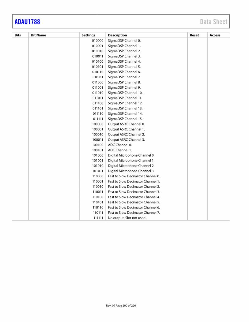
ADAU1788 Data Sheet
Rev. 0 | Page 200 of 226
Bits Bit Name Settings Description Reset Access 010000 SigmaDSP Channel 0. 010001 SigmaDSP Channel 1. 010010 SigmaDSP Channel 2. 010011 SigmaDSP Channel 3. 010100 SigmaDSP Channel 4. 010101 SigmaDSP Channel 5. 010110 SigmaDSP Channel 6. 010111 SigmaDSP Channel 7. 011000 SigmaDSP Channel 8. 011001 SigmaDSP Channel 9. 011010 SigmaDSP Channel 10. 011011 SigmaDSP Channel 11. 011100 SigmaDSP Channel 12. 011101 SigmaDSP Channel 13. 011110 SigmaDSP Channel 14. 011111 SigmaDSP Channel 15. 100000 Output ASRC Channel 0. 100001 Output ASRC Channel 1. 100010 Output ASRC Channel 2. 100011 Output ASRC Channel 3. 100100 ADC Channel 0. 100101 ADC Channel 1. 101000 Digital Microphone Channel 0. 101001 Digital Microphone Channel 1. 101010 Digital Microphone Channel 2. 101011 Digital Microphone Channel 3. 110000 Fast to Slow Decimator Channel 0. 110001 Fast to Slow Decimator Channel 1. 110010 Fast to Slow Decimator Channel 2. 110011 Fast to Slow Decimator Channel 3. 110100 Fast to Slow Decimator Channel 4. 110101 Fast to Slow Decimator Channel 5. 110110 Fast to Slow Decimator Channel 6. 110111 Fast to Slow Decimator Channel 7. 111111 No output. Slot not used.

Data Sheet ADAU1788
Rev. 0 | Page 201 of 226
SERIAL PORT 0 OUTPUT ROUTING SLOT 4 REGISTER Address: 0xC0BB, Reset: 0x3F, Name: SPT0_ROUTE4
Serial Port Output Route Slot 4
111111: No output. Slot not used.110111: Fast to Slow Decimator Channel 7.110110: Fast to Slow Decimator Channel 6.
...000010: FastDSP Channel 2.000001: FastDSP Channel 1.000000: FastDSP Channel 0.
0
11
12
13
14
15
16
07
0
[7:6] RESERVED [5:0] SPT0_OUT_ROUTE4 (R/W)
Table 211. Bit Descriptions for SPT0_ROUTE4 Bits Bit Name Settings Description Reset Access [7:6] RESERVED Reserved. 0x0 R [5:0] SPT0_OUT_ROUTE4 Serial Port Output Route Slot 4. 0x3F R/W 000000 FastDSP Channel 0. 000001 FastDSP Channel 1. 000010 FastDSP Channel 2. 000011 FastDSP Channel 3. 000100 FastDSP Channel 4. 000101 FastDSP Channel 5. 000110 FastDSP Channel 6. 000111 FastDSP Channel 7. 001000 FastDSP Channel 8. 001001 FastDSP Channel 9. 001010 FastDSP Channel 10. 001011 FastDSP Channel 11. 001100 FastDSP Channel 12. 001101 FastDSP Channel 13. 001110 FastDSP Channel 14. 001111 FastDSP Channel 15. 010000 SigmaDSP Channel 0. 010001 SigmaDSP Channel 1. 010010 SigmaDSP Channel 2. 010011 SigmaDSP Channel 3. 010100 SigmaDSP Channel 4. 010101 SigmaDSP Channel 5. 010110 SigmaDSP Channel 6. 010111 SigmaDSP Channel 7. 011000 SigmaDSP Channel 8. 011001 SigmaDSP Channel 9. 011010 SigmaDSP Channel 10. 011011 SigmaDSP Channel 11. 011100 SigmaDSP Channel 12. 011101 SigmaDSP Channel 13. 011110 SigmaDSP Channel 14. 011111 SigmaDSP Channel 15. 100000 Output ASRC Channel 0. 100001 Output ASRC Channel 1. 100010 Output ASRC Channel 2. 100011 Output ASRC Channel 3.

ADAU1788 Data Sheet
Rev. 0 | Page 202 of 226
Bits Bit Name Settings Description Reset Access 100100 ADC Channel 0. 100101 ADC Channel 1. 101000 Digital Microphone Channel 0. 101001 Digital Microphone Channel 1. 101010 Digital Microphone Channel 2. 101011 Digital Microphone Channel 3. 110000 Fast to Slow Decimator Channel 0. 110001 Fast to Slow Decimator Channel 1. 110010 Fast to Slow Decimator Channel 2. 110011 Fast to Slow Decimator Channel 3. 110100 Fast to Slow Decimator Channel 4. 110101 Fast to Slow Decimator Channel 5. 110110 Fast to Slow Decimator Channel 6. 110111 Fast to Slow Decimator Channel 7. 111111 No output. Slot not used.
SERIAL PORT 0 OUTPUT ROUTING SLOT 5 REGISTER Address: 0xC0BC, Reset: 0x3F, Name: SPT0_ROUTE5
Serial Port Output Route Slot 5
111111: No output. Slot not used.110111: Fast to Slow Decimator Channel 7.110110: Fast to Slow Decimator Channel 6.
...000010: FastDSP Channel 2.000001: FastDSP Channel 1.000000: FastDSP Channel 0.
0
11
12
13
14
15
16
07
0
[7:6] RESERVED [5:0] SPT0_OUT_ROUTE5 (R/W)
Table 212. Bit Descriptions for SPT0_ROUTE5 Bits Bit Name Settings Description Reset Access [7:6] RESERVED Reserved. 0x0 R [5:0] SPT0_OUT_ROUTE5 Serial Port Output Route Slot 5. 0x3F R/W 000000 FastDSP Channel 0. 000001 FastDSP Channel 1. 000010 FastDSP Channel 2. 000011 FastDSP Channel 3. 000100 FastDSP Channel 4. 000101 FastDSP Channel 5. 000110 FastDSP Channel 6. 000111 FastDSP Channel 7. 001000 FastDSP Channel 8. 001001 FastDSP Channel 9. 001010 FastDSP Channel 10. 001011 FastDSP Channel 11. 001100 FastDSP Channel 12. 001101 FastDSP Channel 13. 001110 FastDSP Channel 14. 001111 FastDSP Channel 15.

Data Sheet ADAU1788
Rev. 0 | Page 203 of 226
Bits Bit Name Settings Description Reset Access 010000 SigmaDSP Channel 0. 010001 SigmaDSP Channel 1. 010010 SigmaDSP Channel 2. 010011 SigmaDSP Channel 3. 010100 SigmaDSP Channel 4. 010101 SigmaDSP Channel 5. 010110 SigmaDSP Channel 6. 010111 SigmaDSP Channel 7. 011000 SigmaDSP Channel 8. 011001 SigmaDSP Channel 9. 011010 SigmaDSP Channel 10. 011011 SigmaDSP Channel 11. 011100 SigmaDSP Channel 12. 011101 SigmaDSP Channel 13. 011110 SigmaDSP Channel 14. 011111 SigmaDSP Channel 15. 100000 Output ASRC Channel 0. 100001 Output ASRC Channel 1. 100010 Output ASRC Channel 2. 100011 Output ASRC Channel 3. 100100 ADC Channel 0. 100101 ADC Channel 1. 101000 Digital Microphone Channel 0. 101001 Digital Microphone Channel 1. 101010 Digital Microphone Channel 2. 101011 Digital Microphone Channel 3. 110000 Fast to Slow Decimator Channel 0. 110001 Fast to Slow Decimator Channel 1. 110010 Fast to Slow Decimator Channel 2. 110011 Fast to Slow Decimator Channel 3. 110100 Fast to Slow Decimator Channel 4. 110101 Fast to Slow Decimator Channel 5. 110110 Fast to Slow Decimator Channel 6. 110111 Fast to Slow Decimator Channel 7. 111111 No output. Slot not used.

ADAU1788 Data Sheet
Rev. 0 | Page 204 of 226
SERIAL PORT 0 OUTPUT ROUTING SLOT 6 REGISTER Address: 0xC0BD, Reset: 0x3F, Name: SPT0_ROUTE6
Serial Port Output Route Slot 6
111111: No output. Slot not used.110111: Fast to Slow Decimator Channel 7.110110: Fast to Slow Decimator Channel 6.
...000010: FastDSP Channel 2.000001: FastDSP Channel 1.000000: FastDSP Channel 0.
0
11
12
13
14
15
16
07
0
[7:6] RESERVED [5:0] SPT0_OUT_ROUTE6 (R/W)
Table 213. Bit Descriptions for SPT0_ROUTE6 Bits Bit Name Settings Description Reset Access [7:6] RESERVED Reserved. 0x0 R [5:0] SPT0_OUT_ROUTE6 Serial Port Output Route Slot 6. 0x3F R/W 000000 FastDSP Channel 0. 000001 FastDSP Channel 1. 000010 FastDSP Channel 2. 000011 FastDSP Channel 3. 000100 FastDSP Channel 4. 000101 FastDSP Channel 5. 000110 FastDSP Channel 6. 000111 FastDSP Channel 7. 001000 FastDSP Channel 8. 001001 FastDSP Channel 9. 001010 FastDSP Channel 10. 001011 FastDSP Channel 11. 001100 FastDSP Channel 12. 001101 FastDSP Channel 13. 001110 FastDSP Channel 14. 001111 FastDSP Channel 15. 010000 SigmaDSP Channel 0. 010001 SigmaDSP Channel 1. 010010 SigmaDSP Channel 2. 010011 SigmaDSP Channel 3. 010100 SigmaDSP Channel 4. 010101 SigmaDSP Channel 5. 010110 SigmaDSP Channel 6. 010111 SigmaDSP Channel 7. 011000 SigmaDSP Channel 8. 011001 SigmaDSP Channel 9. 011010 SigmaDSP Channel 10. 011011 SigmaDSP Channel 11. 011100 SigmaDSP Channel 12. 011101 SigmaDSP Channel 13. 011110 SigmaDSP Channel 14. 011111 SigmaDSP Channel 15. 100000 Output ASRC Channel 0. 100001 Output ASRC Channel 1. 100010 Output ASRC Channel 2. 100011 Output ASRC Channel 3.

Data Sheet ADAU1788
Rev. 0 | Page 205 of 226
Bits Bit Name Settings Description Reset Access 100100 ADC Channel 0. 100101 ADC Channel 1. 101000 Digital Microphone Channel 0. 101001 Digital Microphone Channel 1. 101010 Digital Microphone Channel 2. 101011 Digital Microphone Channel 3. 110000 Fast to Slow Decimator Channel 0. 110001 Fast to Slow Decimator Channel 1. 110010 Fast to Slow Decimator Channel 2. 110011 Fast to Slow Decimator Channel 3. 110100 Fast to Slow Decimator Channel 4. 110101 Fast to Slow Decimator Channel 5. 110110 Fast to Slow Decimator Channel 6. 110111 Fast to Slow Decimator Channel 7. 111111 No output. Slot not used.
SERIAL PORT 0 OUTPUT ROUTING SLOT 7 REGISTER Address: 0xC0BE, Reset: 0x3F, Name: SPT0_ROUTE7
Serial Port Output Route Slot 7
111111: No output. Slot not used.110111: Fast to Slow Decimator Channel 7.110110: Fast to Slow Decimator Channel 6.
...000010: FastDSP Channel 2.000001: FastDSP Channel 1.000000: FastDSP Channel 0.
0
11
12
13
14
15
16
07
0
[7:6] RESERVED [5:0] SPT0_OUT_ROUTE7 (R/W)
Table 214. Bit Descriptions for SPT0_ROUTE7 Bits Bit Name Settings Description Reset Access [7:6] RESERVED Reserved. 0x0 R [5:0] SPT0_OUT_ROUTE7 Serial Port Output Route Slot 7. 0x3F R/W 000000 FastDSP Channel 0. 000001 FastDSP Channel 1. 000010 FastDSP Channel 2. 000011 FastDSP Channel 3. 000100 FastDSP Channel 4. 000101 FastDSP Channel 5. 000110 FastDSP Channel 6. 000111 FastDSP Channel 7. 001000 FastDSP Channel 8. 001001 FastDSP Channel 9. 001010 FastDSP Channel 10. 001011 FastDSP Channel 11. 001100 FastDSP Channel 12. 001101 FastDSP Channel 13. 001110 FastDSP Channel 14. 001111 FastDSP Channel 15.

ADAU1788 Data Sheet
Rev. 0 | Page 206 of 226
Bits Bit Name Settings Description Reset Access 010000 SigmaDSP Channel 0. 010001 SigmaDSP Channel 1. 010010 SigmaDSP Channel 2. 010011 SigmaDSP Channel 3. 010100 SigmaDSP Channel 4. 010101 SigmaDSP Channel 5. 010110 SigmaDSP Channel 6. 010111 SigmaDSP Channel 7. 011000 SigmaDSP Channel 8. 011001 SigmaDSP Channel 9. 011010 SigmaDSP Channel 10. 011011 SigmaDSP Channel 11. 011100 SigmaDSP Channel 12. 011101 SigmaDSP Channel 13. 011110 SigmaDSP Channel 14. 011111 SigmaDSP Channel 15. 100000 Output ASRC Channel 0. 100001 Output ASRC Channel 1. 100010 Output ASRC Channel 2. 100011 Output ASRC Channel 3. 100100 ADC Channel 0. 100101 ADC Channel 1. 101000 Digital Microphone Channel 0. 101001 Digital Microphone Channel 1. 101010 Digital Microphone Channel 2. 101011 Digital Microphone Channel 3. 110000 Fast to Slow Decimator Channel 0. 110001 Fast to Slow Decimator Channel 1. 110010 Fast to Slow Decimator Channel 2. 110011 Fast to Slow Decimator Channel 3. 110100 Fast to Slow Decimator Channel 4. 110101 Fast to Slow Decimator Channel 5. 110110 Fast to Slow Decimator Channel 6. 110111 Fast to Slow Decimator Channel 7. 111111 No output. Slot not used.
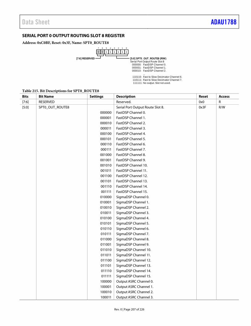
Data Sheet ADAU1788
Rev. 0 | Page 207 of 226
SERIAL PORT 0 OUTPUT ROUTING SLOT 8 REGISTER Address: 0xC0BF, Reset: 0x3F, Name: SPT0_ROUTE8
Serial Port Output Route Slot 8
111111: No output. Slot not used.110111: Fast to Slow Decimator Channel 7.110110: Fast to Slow Decimator Channel 6.
...000010: FastDSP Channel 2.000001: FastDSP Channel 1.000000: FastDSP Channel 0.
0
11
12
13
14
15
16
07
0
[7:6] RESERVED [5:0] SPT0_OUT_ROUTE8 (R/W)
Table 215. Bit Descriptions for SPT0_ROUTE8 Bits Bit Name Settings Description Reset Access [7:6] RESERVED Reserved. 0x0 R [5:0] SPT0_OUT_ROUTE8 Serial Port Output Route Slot 8. 0x3F R/W 000000 FastDSP Channel 0. 000001 FastDSP Channel 1. 000010 FastDSP Channel 2. 000011 FastDSP Channel 3. 000100 FastDSP Channel 4. 000101 FastDSP Channel 5. 000110 FastDSP Channel 6. 000111 FastDSP Channel 7. 001000 FastDSP Channel 8. 001001 FastDSP Channel 9. 001010 FastDSP Channel 10. 001011 FastDSP Channel 11. 001100 FastDSP Channel 12. 001101 FastDSP Channel 13. 001110 FastDSP Channel 14. 001111 FastDSP Channel 15. 010000 SigmaDSP Channel 0. 010001 SigmaDSP Channel 1. 010010 SigmaDSP Channel 2. 010011 SigmaDSP Channel 3. 010100 SigmaDSP Channel 4. 010101 SigmaDSP Channel 5. 010110 SigmaDSP Channel 6. 010111 SigmaDSP Channel 7. 011000 SigmaDSP Channel 8. 011001 SigmaDSP Channel 9. 011010 SigmaDSP Channel 10. 011011 SigmaDSP Channel 11. 011100 SigmaDSP Channel 12. 011101 SigmaDSP Channel 13. 011110 SigmaDSP Channel 14. 011111 SigmaDSP Channel 15. 100000 Output ASRC Channel 0. 100001 Output ASRC Channel 1. 100010 Output ASRC Channel 2. 100011 Output ASRC Channel 3.

ADAU1788 Data Sheet
Rev. 0 | Page 208 of 226
Bits Bit Name Settings Description Reset Access 100100 ADC Channel 0. 100101 ADC Channel 1. 101000 Digital Microphone Channel 0. 101001 Digital Microphone Channel 1. 101010 Digital Microphone Channel 2. 101011 Digital Microphone Channel 3. 110000 Fast to Slow Decimator Channel 0. 110001 Fast to Slow Decimator Channel 1. 110010 Fast to Slow Decimator Channel 2. 110011 Fast to Slow Decimator Channel 3. 110100 Fast to Slow Decimator Channel 4. 110101 Fast to Slow Decimator Channel 5. 110110 Fast to Slow Decimator Channel 6. 110111 Fast to Slow Decimator Channel 7. 111111 No output. Slot not used.
SERIAL PORT 0 OUTPUT ROUTING SLOT 9 REGISTER Address: 0xC0C0, Reset: 0x3F, Name: SPT0_ROUTE9
Serial Port Output Route Slot 9
111111: No output. Slot not used.110111: Fast to Slow Decimator Channel 7.110110: Fast to Slow Decimator Channel 6.
...000010: FastDSP Channel 2.000001: FastDSP Channel 1.000000: FastDSP Channel 0.
0
11
12
13
14
15
16
07
0
[7:6] RESERVED [5:0] SPT0_OUT_ROUTE9 (R/W)
Table 216. Bit Descriptions for SPT0_ROUTE9 Bits Bit Name Settings Description Reset Access [7:6] RESERVED Reserved. 0x0 R [5:0] SPT0_OUT_ROUTE9 Serial Port Output Route Slot 9. 0x3F R/W 000000 FastDSP Channel 0. 000001 FastDSP Channel 1. 000010 FastDSP Channel 2. 000011 FastDSP Channel 3. 000100 FastDSP Channel 4. 000101 FastDSP Channel 5. 000110 FastDSP Channel 6. 000111 FastDSP Channel 7. 001000 FastDSP Channel 8. 001001 FastDSP Channel 9. 001010 FastDSP Channel 10. 001011 FastDSP Channel 11. 001100 FastDSP Channel 12. 001101 FastDSP Channel 13. 001110 FastDSP Channel 14. 001111 FastDSP Channel 15.

Data Sheet ADAU1788
Rev. 0 | Page 209 of 226
Bits Bit Name Settings Description Reset Access 010000 SigmaDSP Channel 0. 010001 SigmaDSP Channel 1. 010010 SigmaDSP Channel 2. 010011 SigmaDSP Channel 3. 010100 SigmaDSP Channel 4. 010101 SigmaDSP Channel 5. 010110 SigmaDSP Channel 6. 010111 SigmaDSP Channel 7. 011000 SigmaDSP Channel 8. 011001 SigmaDSP Channel 9. 011010 SigmaDSP Channel 10. 011011 SigmaDSP Channel 11. 011100 SigmaDSP Channel 12. 011101 SigmaDSP Channel 13. 011110 SigmaDSP Channel 14. 011111 SigmaDSP Channel 15. 100000 Output ASRC Channel 0. 100001 Output ASRC Channel 1. 100010 Output ASRC Channel 2. 100011 Output ASRC Channel 3. 100100 ADC Channel 0. 100101 ADC Channel 1. 101000 Digital Microphone Channel 0. 101001 Digital Microphone Channel 1. 101010 Digital Microphone Channel 2. 101011 Digital Microphone Channel 3. 110000 Fast to Slow Decimator Channel 0. 110001 Fast to Slow Decimator Channel 1. 110010 Fast to Slow Decimator Channel 2. 110011 Fast to Slow Decimator Channel 3. 110100 Fast to Slow Decimator Channel 4. 110101 Fast to Slow Decimator Channel 5. 110110 Fast to Slow Decimator Channel 6. 110111 Fast to Slow Decimator Channel 7. 111111 No output. Slot not used.

ADAU1788 Data Sheet
Rev. 0 | Page 210 of 226
SERIAL PORT 0 OUTPUT ROUTING SLOT 10 REGISTER Address: 0xC0C1, Reset: 0x3F, Name: SPT0_ROUTE10
Serial Port Output Route Slot 10
111111: No output. Slot not used.110111: Fast to Slow Decimator Channel 7.110110: Fast to Slow Decimator Channel 6.
...000010: FastDSP Channel 2.000001: FastDSP Channel 1.000000: FastDSP Channel 0.
0
11
12
13
14
15
16
07
0
[7:6] RESERVED [5:0] SPT0_OUT_ROUTE10 (R/W)
Table 217. Bit Descriptions for SPT0_ROUTE10 Bits Bit Name Settings Description Reset Access [7:6] RESERVED Reserved. 0x0 R [5:0] SPT0_OUT_ROUTE10 Serial Port Output Route Slot 10. 0x3F R/W 000000 FastDSP Channel 0. 000001 FastDSP Channel 1. 000010 FastDSP Channel 2. 000011 FastDSP Channel 3. 000100 FastDSP Channel 4. 000101 FastDSP Channel 5. 000110 FastDSP Channel 6. 000111 FastDSP Channel 7. 001000 FastDSP Channel 8. 001001 FastDSP Channel 9. 001010 FastDSP Channel 10. 001011 FastDSP Channel 11. 001100 FastDSP Channel 12. 001101 FastDSP Channel 13. 001110 FastDSP Channel 14. 001111 FastDSP Channel 15. 010000 SigmaDSP Channel 0. 010001 SigmaDSP Channel 1. 010010 SigmaDSP Channel 2. 010011 SigmaDSP Channel 3. 010100 SigmaDSP Channel 4. 010101 SigmaDSP Channel 5. 010110 SigmaDSP Channel 6. 010111 SigmaDSP Channel 7. 011000 SigmaDSP Channel 8. 011001 SigmaDSP Channel 9. 011010 SigmaDSP Channel 10. 011011 SigmaDSP Channel 11. 011100 SigmaDSP Channel 12. 011101 SigmaDSP Channel 13. 011110 SigmaDSP Channel 14. 011111 SigmaDSP Channel 15. 100000 Output ASRC Channel 0. 100001 Output ASRC Channel 1. 100010 Output ASRC Channel 2. 100011 Output ASRC Channel 3.

Data Sheet ADAU1788
Rev. 0 | Page 211 of 226
Bits Bit Name Settings Description Reset Access 100100 ADC Channel 0. 100101 ADC Channel 1. 101000 Digital Microphone Channel 0. 101001 Digital Microphone Channel 1. 101010 Digital Microphone Channel 2. 101011 Digital Microphone Channel 3. 110000 Fast to Slow Decimator Channel 0. 110001 Fast to Slow Decimator Channel 1. 110010 Fast to Slow Decimator Channel 2. 110011 Fast to Slow Decimator Channel 3. 110100 Fast to Slow Decimator Channel 4. 110101 Fast to Slow Decimator Channel 5. 110110 Fast to Slow Decimator Channel 6. 110111 Fast to Slow Decimator Channel 7. 111111 No output. Slot not used.
SERIAL PORT 0 OUTPUT ROUTING SLOT 11 REGISTER Address: 0xC0C2, Reset: 0x3F, Name: SPT0_ROUTE11
Serial Port Output Route Slot 11
111111: No output. Slot not used.110111: Fast to Slow Decimator Channel 7.110110: Fast to Slow Decimator Channel 6.
...000010: FastDSP Channel 2.000001: FastDSP Channel 1.000000: FastDSP Channel 0.
0
11
12
13
14
15
16
07
0
[7:6] RESERVED [5:0] SPT0_OUT_ROUTE11 (R/W)
Table 218. Bit Descriptions for SPT0_ROUTE11 Bits Bit Name Settings Description Reset Access [7:6] RESERVED Reserved. 0x0 R [5:0] SPT0_OUT_ROUTE11 Serial Port Output Route Slot 11. 0x3F R/W 000000 FastDSP Channel 0. 000001 FastDSP Channel 1. 000010 FastDSP Channel 2. 000011 FastDSP Channel 3. 000100 FastDSP Channel 4. 000101 FastDSP Channel 5. 000110 FastDSP Channel 6. 000111 FastDSP Channel 7. 001000 FastDSP Channel 8. 001001 FastDSP Channel 9. 001010 FastDSP Channel 10. 001011 FastDSP Channel 11. 001100 FastDSP Channel 12. 001101 FastDSP Channel 13. 001110 FastDSP Channel 14. 001111 FastDSP Channel 15.

ADAU1788 Data Sheet
Rev. 0 | Page 212 of 226
Bits Bit Name Settings Description Reset Access 010000 SigmaDSP Channel 0. 010001 SigmaDSP Channel 1. 010010 SigmaDSP Channel 2. 010011 SigmaDSP Channel 3. 010100 SigmaDSP Channel 4. 010101 SigmaDSP Channel 5. 010110 SigmaDSP Channel 6. 010111 SigmaDSP Channel 7. 011000 SigmaDSP Channel 8. 011001 SigmaDSP Channel 9. 011010 SigmaDSP Channel 10. 011011 SigmaDSP Channel 11. 011100 SigmaDSP Channel 12. 011101 SigmaDSP Channel 13. 011110 SigmaDSP Channel 14. 011111 SigmaDSP Channel 15. 100000 Output ASRC Channel 0. 100001 Output ASRC Channel 1. 100010 Output ASRC Channel 2. 100011 Output ASRC Channel 3. 100100 ADC Channel 0. 100101 ADC Channel 1. 101000 Digital Microphone Channel 0. 101001 Digital Microphone Channel 1. 101010 Digital Microphone Channel 2. 101011 Digital Microphone Channel 3. 110000 Fast to Slow Decimator Channel 0. 110001 Fast to Slow Decimator Channel 1. 110010 Fast to Slow Decimator Channel 2. 110011 Fast to Slow Decimator Channel 3. 110100 Fast to Slow Decimator Channel 4. 110101 Fast to Slow Decimator Channel 5. 110110 Fast to Slow Decimator Channel 6. 110111 Fast to Slow Decimator Channel 7. 111111 No output. Slot not used.

Data Sheet ADAU1788
Rev. 0 | Page 213 of 226
SERIAL PORT 0 OUTPUT ROUTING SLOT 12 REGISTER Address: 0xC0C3, Reset: 0x3F, Name: SPT0_ROUTE12
Serial Port Output Route Slot 12
111111: No output. Slot not used.110111: Fast to Slow Decimator Channel 7.110110: Fast to Slow Decimator Channel 6.
...000010: FastDSP Channel 2.000001: FastDSP Channel 1.000000: FastDSP Channel 0.
0
11
12
13
14
15
16
07
0
[7:6] RESERVED [5:0] SPT0_OUT_ROUTE12 (R/W)
Table 219. Bit Descriptions for SPT0_ROUTE12 Bits Bit Name Settings Description Reset Access [7:6] RESERVED Reserved. 0x0 R [5:0] SPT0_OUT_ROUTE12 Serial Port Output Route Slot 12. 0x3F R/W 000000 FastDSP Channel 0. 000001 FastDSP Channel 1. 000010 FastDSP Channel 2. 000011 FastDSP Channel 3. 000100 FastDSP Channel 4. 000101 FastDSP Channel 5. 000110 FastDSP Channel 6. 000111 FastDSP Channel 7. 001000 FastDSP Channel 8. 001001 FastDSP Channel 9. 001010 FastDSP Channel 10. 001011 FastDSP Channel 11. 001100 FastDSP Channel 12. 001101 FastDSP Channel 13. 001110 FastDSP Channel 14. 001111 FastDSP Channel 15. 010000 SigmaDSP Channel 0. 010001 SigmaDSP Channel 1. 010010 SigmaDSP Channel 2. 010011 SigmaDSP Channel 3. 010100 SigmaDSP Channel 4. 010101 SigmaDSP Channel 5. 010110 SigmaDSP Channel 6. 010111 SigmaDSP Channel 7. 011000 SigmaDSP Channel 8. 011001 SigmaDSP Channel 9. 011010 SigmaDSP Channel 10. 011011 SigmaDSP Channel 11. 011100 SigmaDSP Channel 12. 011101 SigmaDSP Channel 13. 011110 SigmaDSP Channel 14. 011111 SigmaDSP Channel 15. 100000 Output ASRC Channel 0. 100001 Output ASRC Channel 1. 100010 Output ASRC Channel 2. 100011 Output ASRC Channel 3.

ADAU1788 Data Sheet
Rev. 0 | Page 214 of 226
Bits Bit Name Settings Description Reset Access 100100 ADC Channel 0. 100101 ADC Channel 1. 101000 Digital Microphone Channel 0. 101001 Digital Microphone Channel 1. 101010 Digital Microphone Channel 2. 101011 Digital Microphone Channel 3. 110000 Fast to Slow Decimator Channel 0. 110001 Fast to Slow Decimator Channel 1. 110010 Fast to Slow Decimator Channel 2. 110011 Fast to Slow Decimator Channel 3. 110100 Fast to Slow Decimator Channel 4. 110101 Fast to Slow Decimator Channel 5. 110110 Fast to Slow Decimator Channel 6. 110111 Fast to Slow Decimator Channel 7. 111111 No output. Slot not used.
SERIAL PORT 0 OUTPUT ROUTING SLOT 13 REGISTER Address: 0xC0C4, Reset: 0x3F, Name: SPT0_ROUTE13
Serial Port Output Route Slot 13
111111: No output. Slot not used.110111: Fast to Slow Decimator Channel 7.110110: Fast to Slow Decimator Channel 6.
...000010: FastDSP Channel 2.000001: FastDSP Channel 1.000000: FastDSP Channel 0.
0
11
12
13
14
15
16
07
0
[7:6] RESERVED [5:0] SPT0_OUT_ROUTE13 (R/W)
Table 220. Bit Descriptions for SPT0_ROUTE13 Bits Bit Name Settings Description Reset Access [7:6] RESERVED Reserved. 0x0 R [5:0] SPT0_OUT_ROUTE13 Serial Port Output Route Slot 13. 0x3F R/W 000000 FastDSP Channel 0. 000001 FastDSP Channel 1. 000010 FastDSP Channel 2. 000011 FastDSP Channel 3. 000100 FastDSP Channel 4. 000101 FastDSP Channel 5. 000110 FastDSP Channel 6. 000111 FastDSP Channel 7. 001000 FastDSP Channel 8. 001001 FastDSP Channel 9. 001010 FastDSP Channel 10. 001011 FastDSP Channel 11. 001100 FastDSP Channel 12. 001101 FastDSP Channel 13. 001110 FastDSP Channel 14. 001111 FastDSP Channel 15.

Data Sheet ADAU1788
Rev. 0 | Page 215 of 226
Bits Bit Name Settings Description Reset Access 010000 SigmaDSP Channel 0. 010001 SigmaDSP Channel 1. 010010 SigmaDSP Channel 2. 010011 SigmaDSP Channel 3. 010100 SigmaDSP Channel 4. 010101 SigmaDSP Channel 5. 010110 SigmaDSP Channel 6. 010111 SigmaDSP Channel 7. 011000 SigmaDSP Channel 8. 011001 SigmaDSP Channel 9. 011010 SigmaDSP Channel 10. 011011 SigmaDSP Channel 11. 011100 SigmaDSP Channel 12. 011101 SigmaDSP Channel 13. 011110 SigmaDSP Channel 14. 011111 SigmaDSP Channel 15. 100000 Output ASRC Channel 0. 100001 Output ASRC Channel 1. 100010 Output ASRC Channel 2. 100011 Output ASRC Channel 3. 100100 ADC Channel 0. 100101 ADC Channel 1. 101000 Digital Microphone Channel 0. 101001 Digital Microphone Channel 1. 101010 Digital Microphone Channel 2. 101011 Digital Microphone Channel 3. 110000 Fast to Slow Decimator Channel 0. 110001 Fast to Slow Decimator Channel 1. 110010 Fast to Slow Decimator Channel 2. 110011 Fast to Slow Decimator Channel 3. 110100 Fast to Slow Decimator Channel 4. 110101 Fast to Slow Decimator Channel 5. 110110 Fast to Slow Decimator Channel 6. 110111 Fast to Slow Decimator Channel 7. 111111 No output. Slot not used.

ADAU1788 Data Sheet
Rev. 0 | Page 216 of 226
SERIAL PORT 0 OUTPUT ROUTING SLOT 14 REGISTER Address: 0xC0C5, Reset: 0x3F, Name: SPT0_ROUTE14
Serial Port Output Route Slot 14
111111: No output. Slot not used.110111: Fast to Slow Decimator Channel 7.110110: Fast to Slow Decimator Channel 6.
...000010: FastDSP Channel 2.000001: FastDSP Channel 1.000000: FastDSP Channel 0.
0
11
12
13
14
15
16
07
0
[7:6] RESERVED [5:0] SPT0_OUT_ROUTE14 (R/W)
Table 221. Bit Descriptions for SPT0_ROUTE14 Bits Bit Name Settings Description Reset Access [7:6] RESERVED Reserved. 0x0 R [5:0] SPT0_OUT_ROUTE14 Serial Port Output Route Slot 14. 0x3F R/W 000000 FastDSP Channel 0. 000001 FastDSP Channel 1. 000010 FastDSP Channel 2. 000011 FastDSP Channel 3. 000100 FastDSP Channel 4. 000101 FastDSP Channel 5. 000110 FastDSP Channel 6. 000111 FastDSP Channel 7. 001000 FastDSP Channel 8. 001001 FastDSP Channel 9. 001010 FastDSP Channel 10. 001011 FastDSP Channel 11. 001100 FastDSP Channel 12. 001101 FastDSP Channel 13. 001110 FastDSP Channel 14. 001111 FastDSP Channel 15. 010000 SigmaDSP Channel 0. 010001 SigmaDSP Channel 1. 010010 SigmaDSP Channel 2. 010011 SigmaDSP Channel 3. 010100 SigmaDSP Channel 4. 010101 SigmaDSP Channel 5. 010110 SigmaDSP Channel 6. 010111 SigmaDSP Channel 7. 011000 SigmaDSP Channel 8. 011001 SigmaDSP Channel 9. 011010 SigmaDSP Channel 10. 011011 SigmaDSP Channel 11. 011100 SigmaDSP Channel 12. 011101 SigmaDSP Channel 13. 011110 SigmaDSP Channel 14. 011111 SigmaDSP Channel 15. 100000 Output ASRC Channel 0. 100001 Output ASRC Channel 1. 100010 Output ASRC Channel 2. 100011 Output ASRC Channel 3.

Data Sheet ADAU1788
Rev. 0 | Page 217 of 226
Bits Bit Name Settings Description Reset Access 100100 ADC Channel 0. 100101 ADC Channel 1. 101000 Digital Microphone Channel 0. 101001 Digital Microphone Channel 1. 101010 Digital Microphone Channel 2. 101011 Digital Microphone Channel 3. 110000 Fast to Slow Decimator Channel 0. 110001 Fast to Slow Decimator Channel 1. 110010 Fast to Slow Decimator Channel 2. 110011 Fast to Slow Decimator Channel 3. 110100 Fast to Slow Decimator Channel 4. 110101 Fast to Slow Decimator Channel 5. 110110 Fast to Slow Decimator Channel 6. 110111 Fast to Slow Decimator Channel 7. 111111 No output. Slot not used.
SERIAL PORT 0 OUTPUT ROUTING SLOT 15 REGISTER Address: 0xC0C6, Reset: 0x3F, Name: SPT0_ROUTE15
Serial Port Output Route Slot 15
111111: No output. Slot not used.110111: Fast to Slow Decimator Channel 7.110110: Fast to Slow Decimator Channel 6.
...000010: FastDSP Channel 2.000001: FastDSP Channel 1.000000: FastDSP Channel 0.
0
11
12
13
14
15
16
07
0
[7:6] RESERVED [5:0] SPT0_OUT_ROUTE15 (R/W)
Table 222. Bit Descriptions for SPT0_ROUTE15 Bits Bit Name Settings Description Reset Access [7:6] RESERVED Reserved. 0x0 R [5:0] SPT0_OUT_ROUTE15 Serial Port Output Route Slot 15. 0x3F R/W 000000 FastDSP Channel 0. 000001 FastDSP Channel 1. 000010 FastDSP Channel 2. 000011 FastDSP Channel 3. 000100 FastDSP Channel 4. 000101 FastDSP Channel 5. 000110 FastDSP Channel 6. 000111 FastDSP Channel 7. 001000 FastDSP Channel 8. 001001 FastDSP Channel 9. 001010 FastDSP Channel 10. 001011 FastDSP Channel 11. 001100 FastDSP Channel 12. 001101 FastDSP Channel 13. 001110 FastDSP Channel 14. 001111 FastDSP Channel 15.

ADAU1788 Data Sheet
Rev. 0 | Page 218 of 226
Bits Bit Name Settings Description Reset Access 010000 SigmaDSP Channel 0. 010001 SigmaDSP Channel 1. 010010 SigmaDSP Channel 2. 010011 SigmaDSP Channel 3. 010100 SigmaDSP Channel 4. 010101 SigmaDSP Channel 5. 010110 SigmaDSP Channel 6. 010111 SigmaDSP Channel 7. 011000 SigmaDSP Channel 8. 011001 SigmaDSP Channel 9. 011010 SigmaDSP Channel 10. 011011 SigmaDSP Channel 11. 011100 SigmaDSP Channel 12. 011101 SigmaDSP Channel 13. 011110 SigmaDSP Channel 14. 011111 SigmaDSP Channel 15. 100000 Output ASRC Channel 0. 100001 Output ASRC Channel 1. 100010 Output ASRC Channel 2. 100011 Output ASRC Channel 3. 100100 ADC Channel 0. 100101 ADC Channel 1. 101000 Digital Microphone Channel 0. 101001 Digital Microphone Channel 1. 101010 Digital Microphone Channel 2. 101011 Digital Microphone Channel 3. 110000 Fast to Slow Decimator Channel 0. 110001 Fast to Slow Decimator Channel 1. 110010 Fast to Slow Decimator Channel 2. 110011 Fast to Slow Decimator Channel 3. 110100 Fast to Slow Decimator Channel 4. 110101 Fast to Slow Decimator Channel 5. 110110 Fast to Slow Decimator Channel 6. 110111 Fast to Slow Decimator Channel 7. 111111 No output. Slot not used.

Data Sheet ADAU1788
Rev. 0 | Page 219 of 226
PDM SAMPLE RATE AND FILTERING CONTROL REGISTER Address: 0xC0DC, Reset: 0x02, Name: PDM_CTRL1
PDM Output Additional InterpolationFiltering Selection
1:delay.More interpolation filtering: higher
0:delay.Less interpolation filtering: lower
PDM Output Path Sample Rate Selection
110: 768 kHz sample rate.101: 384 kHz sample rate.100: 192 kHz sample rate.011: 96 kHz sample rate.010: 48 kHz sample rate.001: 24 kHz sample rate.000: 12 kHz sample rate.
PDM Output Frequency ResponseCompensation
1:
delay).when PDM_MORE_FILT = 1 (higherfor samples rates of 192 kHz or lowerHigh frequency response is compensated
0:(lower delay).High frequency response is not compensated
PDM Output Rate
1: 3.072 MHz PDM output rate.0: 6.144 MHz PDM output rate.
0
01
12
03
04
05
06
07
0
[7] PDM_MORE_FILT (R/W) [2:0] PDM_FS (R/W)
[6:5] RESERVED
[3] PDM_FCOMP (R/W)[4] PDM_RATE (R/W)
Table 223. Bit Descriptions for PDM_CTRL1 Bits Bit Name Settings Description Reset Access 7 PDM_MORE_FILT PDM Output Additional Interpolation Filtering Selection. 0x0 R/W 0 Less interpolation filtering: lower delay. 1 More interpolation filtering: higher delay. [6:5] RESERVED Reserved. 0x0 R 4 PDM_RATE PDM Output Rate. 0x0 R/W 0 6.144 MHz PDM output rate. 1 3.072 MHz PDM output rate. 3 PDM_FCOMP PDM Output Frequency Response Compensation. 0x0 R/W 0 High frequency response is not compensated (lower delay). 1 High frequency response is compensated for samples rates of 192 kHz or lower
when PDM_MORE_FILT = 1 (higher delay).
[2:0] PDM_FS PDM Output Path Sample Rate Selection. 0x2 R/W 000 12 kHz sample rate. 001 24 kHz sample rate. 010 48 kHz sample rate. 011 96 kHz sample rate. 100 192 kHz sample rate. 101 384 kHz sample rate. 110 768 kHz sample rate.

ADAU1788 Data Sheet
Rev. 0 | Page 220 of 226
PDM MUTING, HIGH-PASS, AND VOLUME OPTIONS REGISTER Address: 0xC0DD, Reset: 0xC4, Name: PDM_CTRL2
PDM Output Channel 1 Mute Control
1: PDM output muted.0: PDM output unmuted.
PDM Output Volume Link
1:volume value.All ADC channels use Channel 0
0:volume value.Each ADC channel uses its respective
PDM Output Channel 0 Mute Control
1: PDM output muted.0: PDM output unmuted.
PDM Output Hard Volume
1: Hard/immediate volume change.0: Soft volume ramping.
PDM Output Channel 1 Enable High-PassFilter
1: PDM output high-pass filter on.0: PDM output high-pass filter off. PDM Output Volume Zero Cross Control
1:crossing.Volume change only occurs at zero
0: Volume change occurs at any time.
PDM Output 0 Enable High-PassFilter
1: PDM output high-pass filter on.0: PDM output high-pass filter off.
0
01
02
13
04
05
06
17
1
[7] PDM1_MUTE (R/W) [0] PDM_VOL_LINK (R/W)
[6] PDM0_MUTE (R/W)
[1] PDM_HARD_VOL (R/W)
[5] PDM1_HPF_EN (R/W)
[2] PDM_VOL_ZC (R/W)
[4] PDM0_HPF_EN (R/W)
[3] RESERVED
Table 224. Bit Descriptions for PDM_CTRL2 Bits Bit Name Settings Description Reset Access 7 PDM1_MUTE PDM Output Channel 1 Mute Control. 0x1 R/W 0 PDM output unmuted. 1 PDM output muted. 6 PDM0_MUTE PDM Output Channel 0 Mute Control. 0x1 R/W 0 PDM output unmuted. 1 PDM output muted. 5 PDM1_HPF_EN PDM Output Channel 1 Enable High-Pass Filter. 0x0 R/W 0 PDM output high-pass filter off. 1 PDM output high-pass filter on. 4 PDM0_HPF_EN PDM Output 0 Enable High-Pass Filter. 0x0 R/W 0 PDM output high-pass filter off. 1 PDM output high-pass filter on. 3 RESERVED Reserved. 0x0 R 2 PDM_VOL_ZC PDM Output Volume Zero Cross Control. 0x1 R/W 0 Volume change occurs at any time. 1 Volume change only occurs at zero crossing. 1 PDM_HARD_VOL PDM Output Hard Volume. 0x0 R/W 0 Soft volume ramping. 1 Hard/immediate volume change. 0 PDM_VOL_LINK PDM Output Volume Link. 0x0 R/W 0 Each ADC channel uses its respective volume value. 1 All ADC channels use Channel 0 volume value.

Data Sheet ADAU1788
Rev. 0 | Page 221 of 226
PDM OUTPUT CHANNEL 0 VOLUME REGISTER Address: 0xC0DE, Reset: 0x40, Name: PDM_VOL0
PDM Output Channel 0 Volume Control
11111111: Mute.11111110: −71.25 dB.11111101: −70.875 dB.
...00000010: +23.35 dB.00000001: +23.625 dB.00000000: +24 dB.
0
01
02
03
04
05
06
17
0
[7:0] PDM0_VOL (R/W)
Table 225. Bit Descriptions for PDM_VOL0 Bits Bit Name Settings Description Reset Access [7:0] PDM0_VOL PDM Output Channel 0 Volume Control. 0x40 R/W 00000000 +24 dB. 00000001 +23.625 dB. 00000010 +23.35 dB. 00000011 +22.875 dB. 00000100 +22.5 dB. … … 00111111 +0.375 dB. 01000000 0 dB. 01000001 −0.375 dB. … … 11111101 −70.875 dB. 11111110 −71.25 dB. 11111111 Mute.

ADAU1788 Data Sheet
Rev. 0 | Page 222 of 226
PDM OUTPUT CHANNEL 1 VOLUME REGISTER Address: 0xC0DF, Reset: 0x40, Name: PDM_VOL1
PDM Output Channel 1 Volume Control
11111111: Mute.11111110: −71.25 dB.11111101: −70.875 dB.
...00000010: +23.35 dB.00000001: +23.625 dB.00000000: +24 dB.
0
01
02
03
04
05
06
17
0
[7:0] PDM1_VOL (R/W)
Table 226. Bit Descriptions for PDM_VOL1 Bits Bit Name Settings Description Reset Access [7:0] PDM1_VOL PDM Output Channel 1 Volume Control. 0x40 R/W 00000000 +24 dB. 00000001 +23.625 dB. 00000010 +23.35 dB. 00000011 +22.875 dB. 00000100 +22.5 dB. … … 00111111 +0.375 dB. 01000000 0 dB. 01000001 −0.375 dB. … … 11111101 −70.875 dB. 11111110 −71.25 dB. 11111111 Mute.
PDM OUTPUT CHANNEL 0 ROUTING REGISTER Address: 0xC0E0, Reset: 0x00, Name: PDM_ROUTE0
PDM Output Channel 0 Input Routing
1001011: Digital Microphone Channel 3.1001010: Digital Microphone Channel 2.1001001: Digital Microphone Channel 1.
...0000010: Serial Port 0 Channel 2.0000001: Serial Port 0 Channel 1.0000000: Serial Port 0 Channel 0.
0
01
02
03
04
05
06
07
0
[7] RESERVED [6:0] PDM0_ROUTE (R/W)
Table 227. Bit Descriptions for PDM_ROUTE0 Bits Bit Name Settings Description Reset Access 7 RESERVED Reserved. 0x0 R [6:0] PDM0_ROUTE PDM Output Channel 0 Input Routing. 0x0 R/W 0000000 Serial Port 0 Channel 0. 0000001 Serial Port 0 Channel 1. 0000010 Serial Port 0 Channel 2. 0000011 Serial Port 0 Channel 3. 0000100 Serial Port 0 Channel 4. 0000101 Serial Port 0 Channel 5. 0000110 Serial Port 0 Channel 6. 0000111 Serial Port 0 Channel 7. 0001000 Serial Port 0 Channel 8.

Data Sheet ADAU1788
Rev. 0 | Page 223 of 226
Bits Bit Name Settings Description Reset Access 0001001 Serial Port 0 Channel 9. 0001010 Serial Port 0 Channel 10. 0001011 Serial Port 0 Channel 11. 0001100 Serial Port 0 Channel 12. 0001101 Serial Port 0 Channel 13. 0001110 Serial Port 0 Channel 14. 0001111 Serial Port 0 Channel 15. 0100000 FastDSP Channel 0. 0100001 FastDSP Channel 1. 0100010 FastDSP Channel 2. 0100011 FastDSP Channel 3. 0100100 FastDSP Channel 4. 0100101 FastDSP Channel 5. 0100110 FastDSP Channel 6. 0100111 FastDSP Channel 7. 0101000 FastDSP Channel 8. 0101001 FastDSP Channel 9. 0101010 FastDSP Channel 10. 0101011 FastDSP Channel 11. 0101100 FastDSP Channel 12. 0101101 FastDSP Channel 13. 0101110 FastDSP Channel 14. 0101111 FastDSP Channel 15. 0110000 SigmaDSP Channel 0. 0110001 SigmaDSP Channel 1. 0110010 SigmaDSP Channel 2. 0110011 SigmaDSP Channel 3. 0110100 SigmaDSP Channel 4. 0110101 SigmaDSP Channel 5. 0110110 SigmaDSP Channel 6. 0110111 SigmaDSP Channel 7. 0111000 SigmaDSP Channel 8. 0111001 SigmaDSP Channel 9. 0111010 SigmaDSP Channel 10. 0111011 SigmaDSP Channel 11. 0111100 SigmaDSP Channel 12. 0111101 SigmaDSP Channel 13. 0111110 SigmaDSP Channel 14. 0111111 SigmaDSP Channel 15. 1000000 Input ASRC Channel 0. 1000001 Input ASRC Channel 1. 1000010 Input ASRC Channel 2. 1000011 Input ASRC Channel 3. 1000100 ADC Channel 0. 1000101 ADC Channel 1. 1001000 Digital Microphone Channel 0. 1001001 Digital Microphone Channel 1. 1001010 Digital Microphone Channel 2. 1001011 Digital Microphone Channel 3.
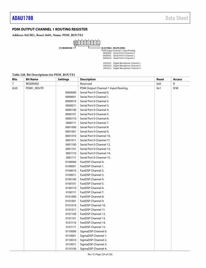
ADAU1788 Data Sheet
Rev. 0 | Page 224 of 226
PDM OUTPUT CHANNEL 1 ROUTING REGISTER Address: 0xC0E1, Reset: 0x01, Name: PDM_ROUTE1
PDM Output Channel 1 Input Routing
1001011: Digital Microphone Channel 3.1001010: Digital Microphone Channel 2.1001001: Digital Microphone Channel 1.
...0000010: Serial Port 0 Channel 2.0000001: Serial Port 0 Channel 1.0000000: Serial Port 0 Channel 0.
0
11
02
03
04
05
06
07
0
[7] RESERVED [6:0] PDM1_ROUTE (R/W)
Table 228. Bit Descriptions for PDM_ROUTE1 Bits Bit Name Settings Description Reset Access 7 RESERVED Reserved. 0x0 R [6:0] PDM1_ROUTE PDM Output Channel 1 Input Routing. 0x1 R/W 0000000 Serial Port 0 Channel 0. 0000001 Serial Port 0 Channel 1. 0000010 Serial Port 0 Channel 2. 0000011 Serial Port 0 Channel 3. 0000100 Serial Port 0 Channel 4. 0000101 Serial Port 0 Channel 5. 0000110 Serial Port 0 Channel 6. 0000111 Serial Port 0 Channel 7. 0001000 Serial Port 0 Channel 8. 0001001 Serial Port 0 Channel 9. 0001010 Serial Port 0 Channel 10. 0001011 Serial Port 0 Channel 11. 0001100 Serial Port 0 Channel 12. 0001101 Serial Port 0 Channel 13. 0001110 Serial Port 0 Channel 14. 0001111 Serial Port 0 Channel 15. 0100000 FastDSP Channel 0. 0100001 FastDSP Channel 1. 0100010 FastDSP Channel 2. 0100011 FastDSP Channel 3. 0100100 FastDSP Channel 4. 0100101 FastDSP Channel 5. 0100110 FastDSP Channel 6. 0100111 FastDSP Channel 7. 0101000 FastDSP Channel 8. 0101001 FastDSP Channel 9. 0101010 FastDSP Channel 10. 0101011 FastDSP Channel 11. 0101100 FastDSP Channel 12. 0101101 FastDSP Channel 13. 0101110 FastDSP Channel 14. 0101111 FastDSP Channel 15. 0110000 SigmaDSP Channel 0. 0110001 SigmaDSP Channel 1. 0110010 SigmaDSP Channel 2. 0110011 SigmaDSP Channel 3. 0110100 SigmaDSP Channel 4.
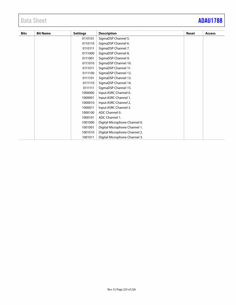
Data Sheet ADAU1788
Rev. 0 | Page 225 of 226
Bits Bit Name Settings Description Reset Access 0110101 SigmaDSP Channel 5. 0110110 SigmaDSP Channel 6. 0110111 SigmaDSP Channel 7. 0111000 SigmaDSP Channel 8. 0111001 SigmaDSP Channel 9. 0111010 SigmaDSP Channel 10. 0111011 SigmaDSP Channel 11. 0111100 SigmaDSP Channel 12. 0111101 SigmaDSP Channel 13. 0111110 SigmaDSP Channel 14. 0111111 SigmaDSP Channel 15. 1000000 Input ASRC Channel 0. 1000001 Input ASRC Channel 1. 1000010 Input ASRC Channel 2. 1000011 Input ASRC Channel 3. 1000100 ADC Channel 0. 1000101 ADC Channel 1. 1001000 Digital Microphone Channel 0. 1001001 Digital Microphone Channel 1. 1001010 Digital Microphone Channel 2. 1001011 Digital Microphone Channel 3.

ADAU1788 Data Sheet
Rev. 0 | Page 226 of 226
OUTLINE DIMENSIONS
04-0
5-20
19-A
A
B
C
D
E
F
0.5300.4700.410
2.7352.6952.655
2.3602.3202.280
12345
BOTTOM VIEW(BALL SIDE UP)
TOP VIEW(BALL SIDE DOWN)
SIDE VIEW
0.2100.1800.150
0.3200.2900.260
0.2800.2400.200
1.75 REF
2.10 REF
0.35BALL PITCH
0.2975
0.285
BALL A1IDENTIFIER
67
COPLANARITY0.05
PKG
-005
423
SEATINGPLANE
Figure 70. 42-Ball Wafer Level Chip Scale Package [WLCSP] (CB-42-2)
Dimensions shown in millimeters
ORDERING GUIDE Model1, 2 Temperature Range Package Description Package Option ADAU1788BCBZRL −40°C to +85°C 42-Ball Wafer Level Chip Scale Package [WLCSP] CB-42-2
1 Z = RoHS Compliant Part.2 ADAU1788 uses the EVAL-ADAU1787Z evaluation board.
I2C refers to a communications protocol originally developed by Philips Semiconductors (now NXP Semiconductors).
©2019 Analog Devices, Inc. All rights reserved. Trademarks and registered trademarks are the property of their respective owners.
D20534-0-8/19(0)