Tunneling in low-power device-design: A bottom-up view of issues ...
108
Tunneling in low-power device-design: A bottom-up view of issues, challenges, and opportunities Kartik Ganapathi Electrical Engineering and Computer Sciences University of California at Berkeley Technical Report No. UCB/EECS-2013-164 http://www.eecs.berkeley.edu/Pubs/TechRpts/2013/EECS-2013-164.html October 3, 2013
Transcript of Tunneling in low-power device-design: A bottom-up view of issues ...
Tunneling in low-power device-design: A bottom-up
view of issues, challenges, and opportunities
Kartik Ganapathi
Electrical Engineering and Computer SciencesUniversity of California at Berkeley
Technical Report No. UCB/EECS-2013-164
http://www.eecs.berkeley.edu/Pubs/TechRpts/2013/EECS-2013-164.html
October 3, 2013

Copyright © 2013, by the author(s).All rights reserved.
Permission to make digital or hard copies of all or part of this work forpersonal or classroom use is granted without fee provided that copies arenot made or distributed for profit or commercial advantage and that copiesbear this notice and the full citation on the first page. To copy otherwise, torepublish, to post on servers or to redistribute to lists, requires prior specificpermission.

Tunneling in low-power device-design: A bottom-up view of issues, challenges, and opportunities
By
Kartik Ganapathi
A dissertation submitted in partial satisfaction of the
requirements for the degree of
Doctor of Philosophy
in
Engineering – Electrical Engineering and Computer Sciences
in the
Graduate Division
of the
University of California Berkeley
Committee in charge:
Professor Sayeef Salahuddin, Chair
Professor Ali Javey
Professor Chenming Hu
Professor Junqiao Wu
Fall 2013

Tunneling in low-power device-design: A bottom-up view of issues, challenges, and opportunities
Copyright © 2013
by
Kartik Ganapathi

1
Abstract
Tunneling in low-power device-design: A bottom-up view of issues, challenges, and opportunities
by
Kartik Ganapathi
Doctor of Philosophy in Engineering - Electrical Engineering and Computer Sciences
University of California, Berkeley
Professor Sayeef Salahuddin, Chair
Simulation of electronic transport in nanoscale devices plays a pivotal role in shedding light on underlying physics, and in guiding device-design and optimization. The length scale of the problem and the physical mechanism of device operation guide the choice of formalism. In the sub-20 nanometer regime, semi-classical approaches start breaking down, thus necessitating a quantum-mechanical treatment of the electronic transport problem. Non-equilibrium Green's function (NEGF) is a theoretical framework for investigating quantum-mechanical systems – interacting with surroundings through exchange of quasiparticles – far from equilibrium. Although hugely computation-intensive with a realistic device-representation, it provides a rigorous way to include particle-particle interactions and to model phenomena that are inherently quantum-mechanical.
We build the Berkeley Quantum Transport Simulator (BQTS) – a massively parallel, generic, NEGF-based numerical simulator – to explore low-power device-design opportunities. Demonstrating scalability and benchmarking results with experimental tunnel diode data, we set out to understand tunneling in devices and to leverage it for both digital and analog applications.
Investigating InAs short-channel band-to-band tunneling transistors (TFETs), we show that direct source-to-drain tunneling sets the leakage-floor in such devices, thereby limiting the minimum subthreshold swing (SS) in spite of excellent electrostatics. A heterojunction TFET with a halo doping in the source-channel overlap region is proposed and is shown to achieve steep SS as well as large ON current. We discover that by band-offset engineering, the steepness therein could be controlled primarily by the modulation of heterojunction-barrier. Subsequently, exploring layered materials for analog applications, we demonstrate that doping the drain underlap region in graphene FETs prolongs the onset of tunneling in their output characteristics, and hence significantly increases their output resistance (r0) and intrinsic gain (gmr0). Due to large bandgap, and consequently, large r0, monolayer-MoS2 FETs exhibit a significant enhancement in maximum oscillation frequency (fmax) over their graphene counterparts.

i
To my parents for all their love, affection, and encouragement
ii
TABLE OF CONTENTS
Chapter 1: Introduction………………………………………………………………………... 1
1.1 Overview………………………………………………………………………….………...1
1.2 Simulation of modern-day semiconductor devices………………………………………... 3
1.3 Non-equilibrium Green’s function based quantum transport……………………………... 5
1.4 Quantum-mechanical tunneling…………………………………………………………… 7
1.5 Some relevant questions……………..……………………………………………………..9
1.6 References………………………………………………………………………………....10
Chapter 2: Berkeley Quantum Transport Simulator……….………………………………..15
2.1 Overview…………………………………………………………………………………..15
2.2 Device structures…………………………………………………………………………..16
2.3 Electronic structure capabilities…………………………………………………………...16
2.3.1 The k.p method………………………………………………………………………..17
2.3.2 The semi-empirical tight-binding method…………………………………………....19
2.4 Self-consistent solution of Pöisson’s and ballistic NEGF equations……………………...21
2.4.1 Pöisson’s equation……………………………………………………………………22
2.4.2 Ballistic NEGF equations…………………………………………………………….23 2.5 Parallelization and Scaling………………………………………………………………...25
2.6 References…………………………………………………………………………………27
Chapter 3: MOSFET simulations – Monolayer Molybdenum disulfide transistors as exemplars……………………...………………………………………………………………...30
3.1 Molybdenum disulfide…………………………………………………………………….30
3.1.1 Material properties……………………………………………………………………30
3.1.2 Transistors of monolayers…………………………………………………………….31
3.2 Short-channel MOSFET simulations……………………………………………………...31
3.2.1 Extraction of parameters from experiments…………………………………………..31
3.2.2 Simulation approach………………………………………………………………….33
3.3 Results and discussion…………………………………………………………………….34
3.3.1 Transfer characteristics……………………………………………………………….34
3.3.2 Output characteristics…………………………………………………………………35
3.3.3 Extrapolation to diffusive regime…………………………………………………….35
3.3.4 Capacitance and density-of-states…………………………………………………….36
iii
3.3.5 Gate oxide and contacts………………………………………………………………38
3.4 Putting it all in perspective………………………………………………………………..39
3.5 Summary…………………………………………………………………………………..40
3.6 References ...………………………………………………………………………………40
Chapter 4: Zener tunneling – Congruence between semi-classical and quantum ballistic formalisms…………..…………………………………………………………………………..43
4.1 Semi-classical or quantum? ………………………………………………………………43
4.2 Simulation approach ……………………………………………………………………...44
4.3 Results and discussion …………………………………………………………………... 45
4.3.1 Heavily doped junctions.……………………………………………………………. 45
4.3.2 Lightly doped junctions ……………………………………………………………...46
4.3.3 Capturing non-uniformity using tight-binding WKB and modified Kane’s models... 46
4.3.4 Comparison with tunnel diode data…………………………………………………. 48
4.4 Summary……………………………………………………………..................................49
4.5 References …………………………………………………………...................................49
Chapter 5: Indium Arsenide lateral and vertical band-to-band tunneling transistors.……52
5.1 Motivation…………………………………………………………................................... 52
5.2 Geometry and simulation details …………………………………………………………52 5.3 Results and discussion …………………………………………………………................54
5.3.1 Transfer characteristics..………………………..……………………………….........54
5.3.2 No vertical tunneling in ultra-thin films……………………………………………...55
5.3.3 Gate length scaling trends……………………………………………........................ 56
5.4 Summary……………………………………………..........................................................57
5.5. References…………………………………………….......................................................57
Chapter 6: Heterojunction vertical tunneling transistors – Steep subthreshold swing with high ON current…………………………………………….......................................................59
6.1 Motivation……………………………………………........................................................59
6.2 Heterojunction VTFET – Simulation details……………………………………………...59
6.3 Results and discussion…………………………………………………………………….60
6.3.1 Transfer characteristics ………………………………………………………………60
6.3.2 OFF state behavior …………………………………………………………………...61
6.3.3 Turn-on mechanism ………………………………………………………………….61
6.3.4 Factors affecting steepness.…………………………………………………………..63
iv
6.3.5 Negative transconductance.………………………………………..…………………64
6.4 Summary..………………………………………………………………………………... 65
6.5 References…....……………………………………………………………………………65
Chapter 7: Graphene transistors – Engineering tunneling to improve output resistance....67 7.1 Graphene transistors for non-digital applications……………………………………...….67
7.2 Simulation approach...…………………………………………………………………….68
7.3 Results and discussion..…………………………………………………………………...69
7.3.1 GFET output characteristics..………………………………………………………...69
7.3.2 Effect of EOT..………………………………………………………………………..70
7.3.3 Effect of Schottky barrier height at the drain contact...………………………………70
7.3.4 Effect of drain underlap length. ..…………………………………………………….70
7.3.5 Effect of n-type doping in the drain underlap region..……………………..…………72
7.3.6 Effect of p-type doping in the drain underlap region..……………………..…………72
7.3.7 Output resistance and intrinsic gain..……………………..…………………………..74
7.3.8 Are quasi-saturation and three-terminal NDR related? ..……………………..……...75
7.3.9 Effect of LG scaling on fT..……………………..…………..……………………..…..75
7.3.10 Effect of EOT scaling on fT ..……………………..…………...…………………….77
7.3.11 Estimation of maximum oscillation frequency..……………………..……………...77
7.4 Summary..……………………..…………..……………………..………………………..78
7.5 References..……………………..…………..……………………..………………………78
Chapter 8: Monolayer MoS2 transistors – Applications beyond switching..……………….81
8.1 Motivation and scope..……………………..…………..……………………..…………...81
8.2 Simulation approach..……………………..…………..……………………..……………82
8.2.1 A two-band k.p Hamiltonian description of monolayer MoS2..……………………...82
8.2.2 Geometry and other parameters..……………………..…………...………………….83
8.3 Results and discussion..……………………..…………...……………………..…………84
8.3.1 Transfer characteristics..……………………..……...……………………..…………84
8.3.2 Output characteristics...……………………..…………...……………………..……..84
8.3.3 Capacitance characteristics..………………………...……………………..…………84
8.3.4 Non-self-consistent calculations from bandstructure..……………………..…………85
8.3.5 Scaling trends of fT and fmax..……………………..…………....……………………..87
8.4 Summary..……………………..…………...……………………..……………………….88
v
8.5 References..……………………..…………...……………………..……………………...88
Chapter 9: Conclusions and future work……………………………………………………..91
9.1 Consolidating what we have learned so far…..…………...……..………………………..91
9.1.1 Comparison between semi-classical and quantum formalisms..….………………….91
9.1.2 Confinement effects..…………………….…………………..……………………….92
9.1.3 Level broadening effects..…………......……………………..……………………….92
9.1.4 Insights in tunnel-FET design..……………..………………..……………………….92
9.1.5 Tunneling insights in MOSFET-design..……………………..…...………………….93
9.2 Future directions..……………………..…………...……………………..……………….93
9.2.1 Dissipative transport..………………....……………………..……………………….93
9.2.2 Density functional theory…………..……………………..…………...…………….. 94
9.2.3 Incorporating gate tunneling and strain..……………………..…………...………….95
9.3 Epilogue..……………………..…………...……………………..………………………..95
9.4 References..……………………..…………...……………………..……………………...95
vi
ACKNOWLEDGEMENTS
First and foremost, I would like to express my deepest sense of gratitude to my advisor, Professor Sayeef Salahuddin. It has been a great privilege to work with him and observe from close quarters the myriad ways in which he attacks a scientific problem. It would not be an overstatement to say that if it were not for his careful grooming during my formative years as a researcher, his constant encouragement to keep setting higher and higher standards for myself, his probing and insightful questions and suggestions, and his eye for new problems, this thesis would not have taken the shape it has today. I will forever remain grateful to him for all the learning experiences interactions with him and working in his group have offered me over the course of my Berkeley years.
I would like to thank Professors Ali Javey, Chenming Hu and Junqiao Wu for gladly accepting to be on my qualifying exam and dissertation committees, and for providing invaluable suggestions and comments during this course. Also, I would like to express my sincerest thanks to Professor Javey for all the help from time to time – often going out of his way – in addition to the learning opportunities I had as a research collaborator, and as a GSI for his class. I am also thankful to Professor Hu for all the interesting and stimulating discussions we had during the DARPA STEEP days, which is when my interest in tunneling phenomenon started blooming.
I am indebted to Professor Youngki Yoon, my long time collaborator, with whom I had the chance to work on a variety of research projects and to share my excitement about several small-but-pleasing discoveries along the way. I would also like to thank Professor Mark Lundstrom for some intriguing discussions we had during our collaboration on graphene transistors.
I am grateful to SRC Education Alliance and GlobalFoundries for the internship opportunity during the summer of 2012. I would like to thank Drs. Ajey Jacob and Bhagawan Sahu for mentoring me and providing a glimpse of industrial research, in addition to hosting me in Albany, NY and helping during the entire period in ways more than one. My sincere thanks are also due to Drs. Zoran Krivokapic and Steven Bentley for many a thought-provoking technical discussion on III-V transistors.
I am very thankful to Intel Corporation for the PhD Fellowship they offered me during 2012-13. In this context, I would like to thank Dr. Ian Young and my fellowship mentor, Dr. Uygar Avci, for opportunities they provided to present my research to their group both in person and via teleconferences. I am hugely indebted to Dr. Dmitri Nikonov for his very generous help in recommending me to the fellowship.
I have had the good fortune of interacting with some very bright and talented colleagues from LEED and Device groups in Berkeley, and of learning a great deal from them. In particular, I would like to express my thanks to Asif I. Khan, Khalid Ashraf, Debanjan Bhowmik, Samuel Smith, Varun Mishra, Rumi Karim, Nattapol Damrongplasit, Sriramkumar Venugopalan, Rehan Kapadia, Sapan Agarwal, Sung Hwan Kim and Peter Matheu for several interesting conversations at workplace, technical or otherwise.
Also, outside workplace, I was lucky enough to make some very good friends at Berkeley and in the bay area, all of who, in some way or the other, have helped me endure difficult times and

vii
have been instrumental in helping me gain a broad perspective on various aspects of life. I would like to express my heartfelt gratitude to Kaustubh Joshi, Pranav Shah, Sudeep Kamath, Pavan Hosur, Sudeep Juvekar, Rutooj Deshpande, Dhawal Mujumdar, Mangesh Bangar, Anuj Tewari, Shaama M. S., Sarika Goel, Sameer Agarwal, Deepan Raj Prabakar, Debanjan Mukherjee, Sharanya Prasad, Aditya Medury, Ankit Jain, Avinash Bharadwaj, Chintan Thakkar, Vivek Ramamurthy, Nitesh Jain, Arunanshu Roy, Venkatesan Ekambaram, Ashwin Kashyap, and Abhinav Gaikwad for being the wonderfully warm and genuine people they are.
And last but not the least, words fail me in conveying indebtedness to my parents – Ganapati Ramakrishna Bhat and Saraswati Bhat – whose love, affection, encouragement, and unflinching confidence in my abilities forever motivate me to keep striving for excellence in every endeavor. This work is a dedication to all their sacrifices that have brought me to where I am today.
1
CHAPTER 1
INTRODUCTION In this chapter, we begin with a brief overview of the challenges and opportunities associated with low-power device-design. Subsequently, we examine the necessary considerations in choosing the electronic transport formalism to investigate next-generation of energy-efficient transistors. We then provide a summary of the non-equilibrium Green’s function based quantum transport formalism, which is the approach we use during the course of this study. Finally, after examining various efforts reported in the literature on using tunneling as a means to achieving lower power consumption, we outline the questions that we hope to answer in the subsequent chapters.
1.1 OVERVIEW
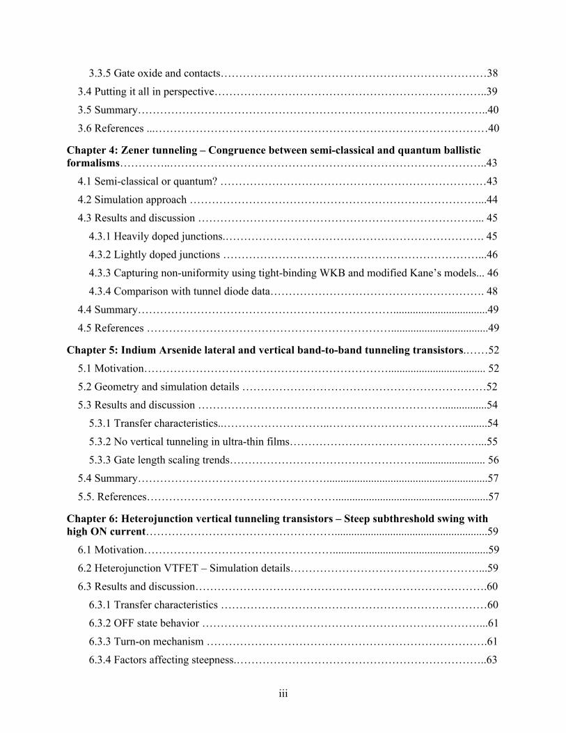
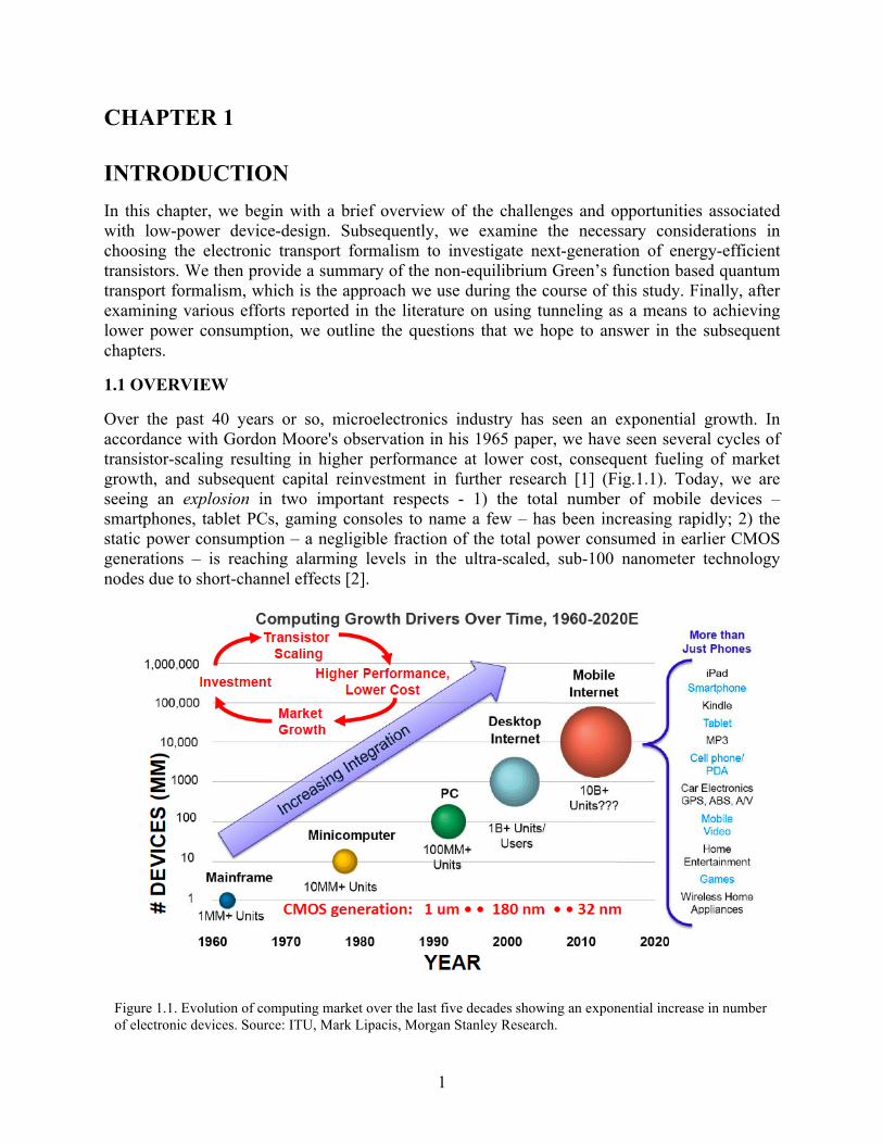
Over the past 40 years or so, microelectronics industry has seen an exponential growth. In accordance with Gordon Moore's observation in his 1965 paper, we have seen several cycles of transistor-scaling resulting in higher performance at lower cost, consequent fueling of market growth, and subsequent capital reinvestment in further research [1] (Fig.1.1). Today, we are seeing an explosion in two important respects - 1) the total number of mobile devices – smartphones, tablet PCs, gaming consoles to name a few – has been increasing rapidly; 2) the static power consumption – a negligible fraction of the total power consumed in earlier CMOS generations – is reaching alarming levels in the ultra-scaled, sub-100 nanometer technology nodes due to short-channel effects [2].
Figure 1.1. Evolution of computing market over the last five decades showing an exponential increase in number of electronic devices. Source: ITU, Mark Lipacis, Morgan Stanley Research.

2
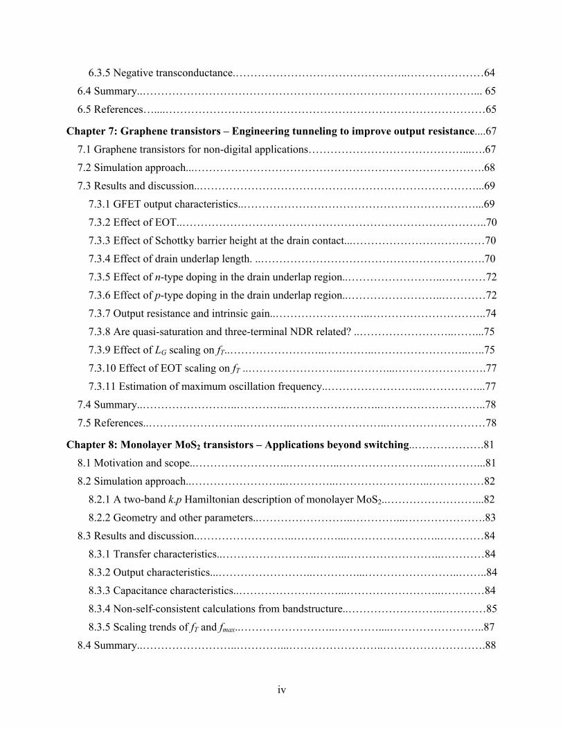
With the proliferation of technology and increase in people’s computing needs, it can be expected that in future, demands on cloud computing, which fuels most of the high-performance computing today, would increase. Additionally, it is envisioned that we would reach an era of immersive computing where a large number of physically standalone devices (e.g., wireless sensor networks, wearable electronics) would augment our sensory perceptions of physical reality [3](Fig.1.2).
Thus, the motivation to investigate design of energy-efficient, low-power electronic devices and systems is threefold – (a) the global non-renewable, fossil fuel reserves are anticipated to deplete
Figure 1.2. A speculative view of the future of low-power electronics – a swarm of physically standalone devices increasing the number of ways in which we interact with our surroundings (top); a huge number of wearable devices (bottom), necessitating energy-efficient computing (adapted from Ref. [3]).
3
to discomfortingly low levels in the coming few decades; (b) the share of electronics in people’s energy consumption requirements is increasing, and (c) the battery life of devices, particularly in cases such as medical implants (cochlear implant, artificial cardiac pacemaker etc.), wireless sensors deployed in remote areas to name a few, is critical. Hence it is unsurprising that, in addition to finding renewable, clean and sustainable ways of electric power generation as a means to address some of the above concerns, a great volume of research is directed towards designing next-generation of power-parsimonious electronics through innovations not only at the transistor level, but also at circuit and system levels [4]-[6].
In this thesis, however, our focus will be on underlining issues and challenges at the former level and on investigating opportunities that a combination of low-dimensional material-systems and non-conventional switching mechanisms provides in achieving that goal. The following explanatory points are in order here –
Firstly, in appreciating the underlying bottlenecks in any engineering design problem, it is imperative that we make the following distinction between two loosely defined classes of challenges. The first class is categorized by issues that are either fundamental to the physical mechanism of interest or are due to some intrinsic, difficult-to-tune properties of the materials under consideration – e.g., Boltzmann tyranny in conventional metal-oxide-semiconductor field-effect transistors (MOSFETs), leakage current limitations due to absence of bandgap in graphene etc. [7]. The second category is those of challenges that are more closely associable with translation of a proof-of-concept or theoretical demonstration to a commercially viable technology - e.g., CMOS process compatibility, lithography-related scaling issues etc. While we do not undermine the importance of addressing the second class of problems, our motivation to focus on the first category is guided by the following heuristics – (a) in identifying challenges and opportunities for technologies distantly away on the roadmap, it is of practical significance to focus on this class so that the vast exploration-space is sufficiently narrowed, and (b) our experience – gained as a community over the past decades in driving Moore’s law – gives reasons to be optimistic of overcoming challenges of second kind, provided the promised gains of a given scientific idea command its technologization.
Secondly, guided by the same spirit, this work – barring occasions when we either compare with or provide explanations to experimental observations – draws heavily upon simulation, which has emerged as the third pillar of scientific enquiry – theory and experiment being the other two – enabling headways in problems considered resistive to latter approaches [8]. While there exist several interesting physical problems – the celebrated spin-glass problem and computation of the universal functional in density functional theory being the classic exemplars – which have been shown to be computationally intractable (with increasing degrees of freedom) using classical computers, most problems of interest to us in electronic transport simulation – which involve low-energy excitations of a quantum many-body system – do not fall into this category and are amenable to perturbative methods with certain approximations [9]-[11]. The theoretical framework for our simulation will be described in greater detail in subsequent sections.
1.2 SIMULATION OF MODERN-DAY SEMICONDUCTOR DEVICES
The need to accurately predict device performance via simulations has, perhaps, never been as important as it is today, with fabrication complexity of modern-day semiconductor devices continuously increasing, resulting in several challenges relating to yield and variability.
4
However, even in the simulation domain, there exist considerable issues concerning computation time and memory requirements.
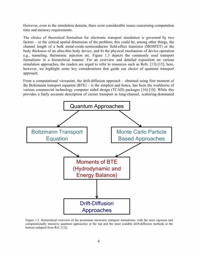
The choice of theoretical formalism for electronic transport simulation is governed by two factors – a) the critical spatial dimension of the problem; this could be, among other things, the channel length of a bulk metal-oxide-semiconductor field-effect transistor (MOSFET) or the body thickness of an ultra-thin body device, and b) the physical mechanism of device operation e.g., tunneling, thermionic injection etc. Figure 1.3 depicts the commonly used transport formalisms in a hierarchical manner. For an overview and detailed exposition on various simulation approaches, the readers are urged to refer to resources such as Refs. [13]-[15]; here, however, we highlight some key considerations that guide our choice of quantum transport approach.
From a computational viewpoint, the drift-diffusion approach – obtained using first moment of the Boltzmann transport equation (BTE) – is the simplest and hence, has been the workhorse of various commercial technology computer aided design (TCAD) packages [16]-[18]. While this provides a fairly accurate description of carrier transport in long-channel, scattering-dominated
Figure 1.3. Hierarchical overview of the prominent electronic transport formalisms, with the most rigorous and computationally intensive quantum approaches at the top and the most scalable drift-diffusion methods at the bottom (adapted from Ref. [12]).
Quantum Approaches
Boltzmann Transport Equation
Monte Carlo Particle Based Approaches
Moments of BTE (Hydrodynamic and
Energy Balance)
Drift-Diffusion Approaches
5
(diffusive) devices wherein the electric fields are small, it fails to capture hot-carrier effects like velocity overshoot, that affect the device performance considerably in the sub-100 nm channel-length regime [19]. In order to account for these, one needs to move to hydrodynamic and energy-balance models, which happen to be higher moments of BTE. However, moment-based solutions to BTE lose their validity with increase in electric field strength and could result in spurious velocity peaks due to truncation of moments – which, in theory, are infinite in number – to a finite number [20].
The resolution of issues arising due to these continuum models of transport is achieved by solving the full-blown BTE itself, wherein the most common approach is using particle-based Monte Carlo methods – discussed extensively in literature viz. Refs. [21], [22]. While these techniques provide a reliable and accurate way to understand transport behavior in ultra-scaled transistors, including phenomenon like self-heating – common in silicon-on-insulator (SOI) devices – their correctness is still limited to the semi-classical regime i.e., when the electrostatic potential within the device is varying smoothly on the order of the quasi-particle De Broglie wavelength. With device dimensions continuously shrinking, present-generation transistors are already at a stage where, in certain non-silicon material-systems like III-V semiconductors with much smaller carrier effective mass, the semi-classical approximation is breaking down. This, coupled with our interest in leveraging tunneling – a phenomenon with no classical analogue – for low-power device design, motivates us to adopt the most computation-intensive quantum transport approaches. We describe one such formalism – non-equilibrium Green’s function (NEGF) in the subsequent section, which we use throughout the rest of the report for simulation purposes.
1.3 NON-EQUILIBRIUM GREEN’S FUNCTION BASED QUANTUM TRANSPORT
Non-equilibrium Green’s function (NEGF) approach is a generic theoretical framework for investigating quantum-mechanical systems far from equilibrium. With device dimensions believed to enter the sub-10 nm regime in the near future, it has emerged as the most acceptably rigorous way to understand carrier transport mechanisms at such length-scales [23]. A detailed introduction to the fundamentals of the formalism – developed through the seminal works on quantum many-body physics of Martin and Schwinger [24], Kadanoff and Baym [25], Keldysh [26] – can be found in Refs. [23] and [27]. Here we only provide a brief overview of the formalism for the sake of completeness.
In a nutshell, NEGF is a compact scheme for determining the response of an open system – typically driven outside equilibrium – which couples to external reservoirs with which it can exchange quasi-particles like electrons (e.g., in case of an electrochemical cell), photons (a light source), phonons (crystal lattice) etc. While esoteric scenarios involving reservoirs themselves being driven out of equilibrium could, in principle, be handled within the framework, in cases of our interest, the equilibrium assumption on reservoirs suffices. This implies we can assign equilibrium ensemble-measures such as electrochemical potential (µ) and temperature (T) to them. However, such assignments are not made for the system (device), which is assumed to be small enough so that similar statistics do not hold.
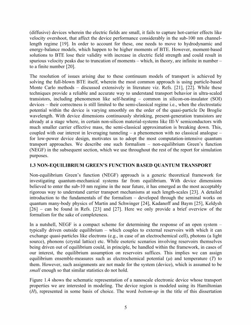
Figure 1.4 shows the schematic representation of a nanoscale electronic device whose transport properties we are interested in modeling. The device region is modeled using its Hamiltonian (H), represented in some basis of choice. The word bottom-up in the title of this dissertation
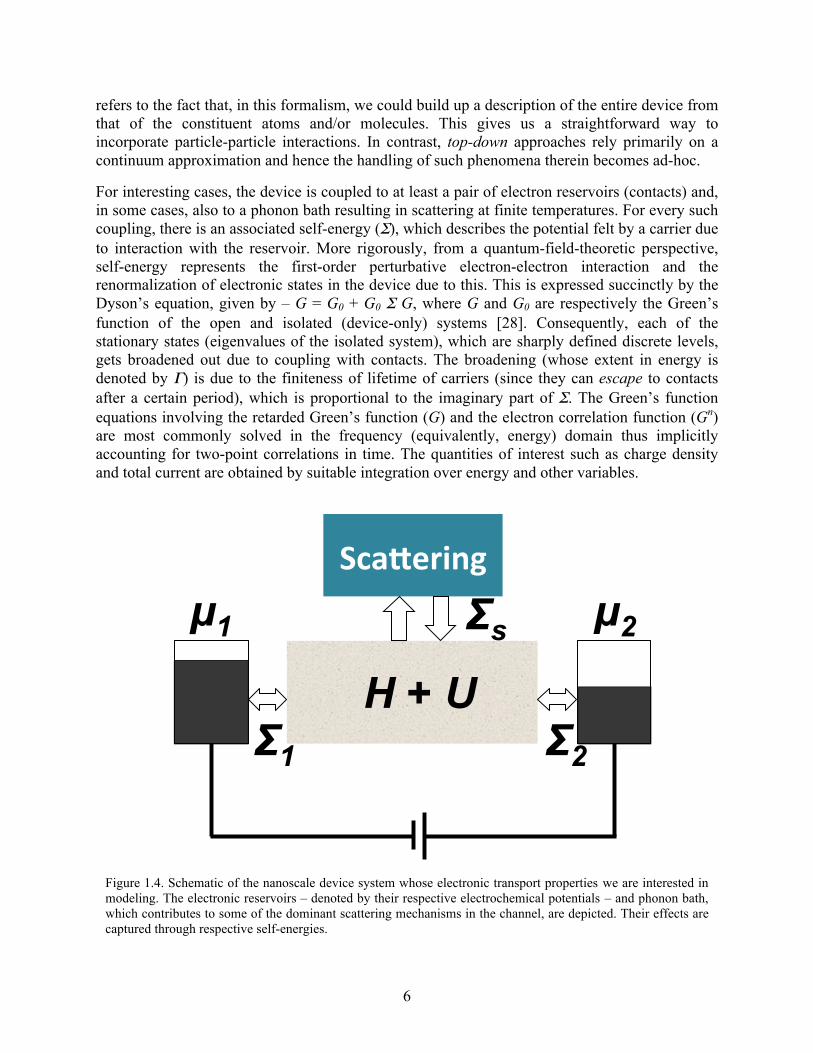
6
refers to the fact that, in this formalism, we could build up a description of the entire device from that of the constituent atoms and/or molecules. This gives us a straightforward way to incorporate particle-particle interactions. In contrast, top-down approaches rely primarily on a continuum approximation and hence the handling of such phenomena therein becomes ad-hoc.
For interesting cases, the device is coupled to at least a pair of electron reservoirs (contacts) and, in some cases, also to a phonon bath resulting in scattering at finite temperatures. For every such coupling, there is an associated self-energy (Σ), which describes the potential felt by a carrier due to interaction with the reservoir. More rigorously, from a quantum-field-theoretic perspective, self-energy represents the first-order perturbative electron-electron interaction and the renormalization of electronic states in the device due to this. This is expressed succinctly by the Dyson’s equation, given by – G = G0 + G0 Σ G, where G and G0 are respectively the Green’s function of the open and isolated (device-only) systems [28]. Consequently, each of the stationary states (eigenvalues of the isolated system), which are sharply defined discrete levels, gets broadened out due to coupling with contacts. The broadening (whose extent in energy is denoted by Γ) is due to the finiteness of lifetime of carriers (since they can escape to contacts after a certain period), which is proportional to the imaginary part of Σ. The Green’s function equations involving the retarded Green’s function (G) and the electron correlation function (Gn) are most commonly solved in the frequency (equivalently, energy) domain thus implicitly accounting for two-point correlations in time. The quantities of interest such as charge density and total current are obtained by suitable integration over energy and other variables.
Figure 1.4. Schematic of the nanoscale device system whose electronic transport properties we are interested in modeling. The electronic reservoirs – denoted by their respective electrochemical potentials – and phonon bath, which contributes to some of the dominant scattering mechanisms in the channel, are depicted. Their effects are captured through respective self-energies.
!"#$%&'()*
H + U
µ1 µ2
!1 !2
!s
7
The electrostatic potential (U) is another important piece of the puzzle due to our interest far away from equilibrium where its effect is non-negligible. As long as device dimensions are not extremely small, to the extent of rendering the single-electron charging energy (U0) to be larger than contact-induced broadening (Γ) and thermal broadening (kBT, with kB being the Boltzmann constant) – the well-known self-consistent field (SCF) regime – we can include U in the Green’s function calculations through self-consistent solutions of NEGF and Poisson’s equations. We shall turn to discussion of equations and the associated computational challenges in a detailed manner in Chapter 2. However, for the remainder of this chapter, we will focus our discussion on yet another key topic in the title, tunneling, which happens to be the common thread across several pieces of this work.
1.4 QUANTUM-MECHANICAL TUNNELING
Tunneling is, arguably, one of most extensively studied quantum-mechanical phenomena ever since the advent of quantum mechanics in earlier part of the previous century. Experimental evidence of tunneling – a manifestation of the wave-particle duality, with particle having a decaying-but-finite probability in the classically forbidden region – has been observed in a plethora of physical systems – from condensed-matter to high-energy. Needless to say, a large number of practical applications have been built leveraging tunneling, some of which we shall discuss briefly in the remainder of this section and hence motivate the readers towards the role of tunneling in recent low-power device-design efforts.
In solids, tunneling comes about in various flavors depending on – a) the quasi-particle under consideration – electron- and hole-tunneling in semiconductors, tunneling of Cooper pairs in superconducting Josephson junctions; b) the initial and final states of the carriers – band-to-band tunneling, intra-band tunneling; c) shape of the potential barrier through which tunneling occurs – Fowler-Nordheim tunneling, direct tunneling (most commonly in tunneling through gate-oxide of modern-day MOSFETs); d) the mediator for tunneling – trap-, impurity- and phonon-assisted tunneling; e) the number of tunnel-barriers – resonant tunneling, second and higher-order co-tunneling effects in cascaded tunnel junctions (commonly in quantum-dots and single-electron transistors (SETs)) [29]-[32]. Each of these mechanisms is interesting in its own right and has ramifications in real-world applications – e.g., gate-oxide tunneling is one of the major leakage and oxide-degradation mechanisms posing OFF-state current and reliability concerns in ultra-scaled FETs, the negative-differential resistance (NDR) in current-voltage characteristics of III-V resonant tunneling diodes could be used for electrical gain in optoelectronic devices, co-tunneling is a source of errors in SETs, among others [33]-[35]. However, our primary focus in this report will be on band-to-band tunneling i.e., carrier tunneling from valence to conduction band of a semiconductor, which has emerged as a mechanism to design low-power transistors in recent times.
The first theoretical investigation of tunneling in solids (for 1-D case) was done by Clarence Zener, where he calculated the probability of transition of carriers into excited bands under high electric fields [36]. Subsequently, Keldysh and Kane calculated the tunneling rate for the case of constant electric field across a p-n junction, with the inclusion of transverse crystal momenta – conserved during tunneling – in their treatments [37], [38]. In addition, their calculations involved greater rigor in terms evaluating the action integral near the branch point – where conduction and valence bands merge for some imaginary wavevector – thereby accurately
8
computing the transition rates. However, the closed-form, analytical expressions derived by them in case of direct bandgap semiconductors hold only under the approximations of semiclassicality and of parabolic dispersion in both conduction and valence bands. In a later paper, Kane extended his treatment to the case of indirect tunneling – where the transitions occur across the indirect bandgap with the emission or absorption of phonons – resulting in an expression similar to the direct tunneling case [39]. This, together with his discussion on extension of these arguments to include effects such as variable field, non-parabolicity of electronic structure, presence of bandgap states etc. formed the mainstay of our understanding of tunneling and its modeling, in various forms, in TCAD device simulators until fairly recently when we could investigate the phenomenon in the full quantum-mechanical sense, in realistic device dimensions with a sufficiently elaborate electronic structure description.
On the experimental front, the one of the first demonstrations of tunneling was by Esaki in forward-biased, heavily doped, narrow germanium p-n junctions [40]. Since then, the robustness of tunneling phenomenon in two-terminal devices as been comprehensively established with its observation in a wide range of ranging from III-V homo- and hetero-junctions (Refs. [41]-[43]), graphene and its nanostructures (Refs. [44], [45]), oxides of rare earth metals (Ref. [46]), superlattices (Ref. [47]) to name a few. Consequently, the effect has been used for various applications – both in forward- (NDR region) and reverse-bias regimes – such as in voltage regulators, high-speed microwave circuits, multi-junction solar cells, lasers etc [48], [49].
One of the earliest proposals to leverage tunneling in a three-terminal device is due to Chang and Esaki, who put forth the idea of a tunneling-base transistor wherein the relatively short tunneling time in the base was expected to increase the current gain [50]. However, requirements of right heterostructure band-offsets and device dimensions imposed severe restrictions on fabrication. Later, Quinn et al. suggested voltage-controlled modulation of tunneling probability by replacing the doping of a MOSFET source from n+- to p+-type – a structure investigated widely in subsequent years in the context of low subthreshold swing (SS) devices – as spectroscopic tool to probe 2-D channel states [51]. The experimental demonstrations of field-effect-dependent tunneling behavior were done by Baba in GaAs-based p+-p-n+ devices [52] and later by Koga and Toriumi in a Si system [53], who showed, along the lines of the bipolar tunnel FET proposed by Leburton et al. [54], a modulation of the NDR region with changing gate voltage.
The idea behind using band-to-band tunneling transistors, the discussion of which will form a significant portion of this study, is that the crossing and uncrossing of conduction and valence bands in close spatial proximity – the same phenomenon that gives rise to NDR in two-terminal junctions – can be effectively modulated using gate-induced vertical field in an MOS structure. The ability of such devices to circumvent Boltzmann tyranny arises from the fact that the carrier concentration on the source side (e.g., degenerately doped p-type material) follows a non-Boltzmann-like (and hence non-equilibrium) distribution due to clipping of part of the Fermi-tail due to the semiconductor bandgap (Fig. 1.5). Appenzeller et al. provided the first experimental confirmation of using this concept to achieve less than 60 mV/decade of SS at room temperature through carbon nanotube tunneling field-effect transistors (TFETs) that exhibited 40 mV/decade swing [56]. Some of the earliest results showing less than 60 mV/decade SS in other material systems have been by Choi et al. in Si TFETs [57], by Krishnamohan et al. in Ge [58], and by Kim et al. in p+ Ge/n+ Si devices [59]. For a more comprehensive overview on the status of TFET research until circa 2010, the readers are suggested to refer to the review article by

9
Seabaugh and Zhang [60] and the references therein. However, here we present a summary of the major challenges in order to motivate our studies in the upcoming chapters.
Figure 1.6 (Fig. 2 of Ref. [60]) shows the experimental switching characteristics of both p- and n-channel TFETs reported in various studies compared against those of the state-of-the-art 32-nm conventional CMOS technology. It is imperative to infer that on the experimental front, the TFETs are at a fairly nascent stage in becoming a viable alternative for next-generation low-power technologies – a) reliable, reproducible results exhibiting less than 60 mV/decade have been few; b) due to the very nature of TFETs – huge tunneling resistance in ON state – the ON current is significantly less; c) the ON-OFF ratios in devices with large ON current – III-V-based TFETs in particular – are severely degraded; d) the SS, even in cases where they are than 60 mV/dec, have been mostly in the range of 40-50 mV/decade. However, simulation studies on TFETs (e.g. Refs. [61]-[64]), primarily the ones using semi-classical formalisms – WKB, Kane and their variants to name a few – have been overly optimistic in their projections of device performance in general and SS, ON current and ON-OFF ratios in particular (refer to Fig. 3 of Ref. [60] for an overview of various TFET-simulation reports).
1.5 SOME RELEVANT QUESTIONS
Given this context, it becomes pertinent to answer the following questions – a) with a rigorous representation of the atomistic properties of the system, what kind of device performance could be expected? b) Are there any fundamental bottlenecks or design trade-offs that are not manifestly apparent through simpler models? c) Under what conditions/ length-scales does the correspondence between semi-classical and quantum formalisms of tunneling hold? d) How do the effects of confinement and level broadening affect TFET design considerations? e) Can the insights on tunneling, gleaned from understanding TFETs, be used to design better MOSFETs for non-switching applications in certain novel material-systems? The quest for answers to these questions guides our discussion in the remainder of this report. Before we jump into the specific device physics aspects, we shall take a detour in Chapter 2 to detail the development of a
Figure 1.5. Schematic showing the physical mechanisms of operation of MOSFET (left) and Tunnel FET (right) (adapted from Ref. [55]). MOSFETs operate through thermionic emission over the barrier in the channel and thus have a fundamental limit in the steepness of switching. TFETs cut-off part of the Fermi-Dirac distribution of carriers in the source through the bandgap and hence overcome this limitation.
TTuunnnneell FFEETT MOSFET

10
massively parallel, NEGF-based quantum transport simulator that we use to address the above questions.
1.6 REFERENCES
[1] G. E. Moore, “Cramming more components onto integrated circuits,” Electronics Magazine, vol. 38, no. 8, 1965.
[2] N. S. Kim, T. Austin, D. Baauw, T. Mudge, K. Flautner, J. S. Hu, and V. Narayanan, “Leakage current: Moore's law meets static power,” Computer, vol. 36, no. 12, pp. 68-75, 2003.
[3] J. M. Rabaey, “The swarm at the edge of the cloud-A new perspective on wireless,” IEEE Symp. on VLSI circuits (VLSIC), pp. 6-8, 2011.
[4] E. A. Vittoz, “Low-power design: ways to approach the limits,” International Solid-State Circuits Conference (ISSCC) Tech. Dig., pp. 14-18, 1994.
[5] J. M. Rabaey, “Low power design essentials,” Springer, 2009.
Figure 1.6. Experimental switching characteristics of p-type (left) and n-type (right) TFETs from various studies that have reported SS of less than 60 mV/decade (from Ref. [60]). The characteristics for state-of-the-art 32-nm node CMOS technology are also shown for the purposes of comparison.
11
[6] D. Markovic, C. C. Wang, L. P. Alarcon, T. -T. Liu, and J. M. Rabaey “Ultralow-power design in near-threshold region,” Proc. IEEE, vol. 98, no. 2, pp. 237-252, 2010.
[7] S. Salahuddin and S. Datta, “Use of negative capacitance to provide voltage amplification for low power nanoscale devices,” Nano Lett., vol. 8, no. 2, pp. 405-410, 2008.
[8] L. P. Kadanoff, “Excellence in computer simulation,” Comput. Sci. Eng., vol. 6, no. 2, pp. 57-67, 2004.
[9] R. B. Laughlin, “The physical basis of computability,” Comput. Sci. Eng., vol. 4, no. 3, pp. 27-30, 2002.
[10] S. Aaronson, “Computational complexity: Why quantum chemistry is hard,” Nat. Phys., vol. 5, no. 10, pp. 707-708, 2009.
[11] M. M. Wolf, “Quantum many-body theory: Divide, perturb and conquer,” Nat. Phys., vol. 4, no. 11, pp. 834-835, 2008.
[12] D. Vasileska (2001, Spring), “Introduction to Modeling,” [Online]. Available: http://www.eas.asu.edu/~vasilesk/EEE533/lecture2.ppt
[13] D. Vasileska, D. Mamaluy, H. R. Khan, K. Raleva and S. M. Goodnick, “Semiconductor Device Modeling,” J. Comput. Theor. Nanos., vol. 5, no. 6, p. 999, 2008.
[14] M. Lundstrom, “Fundamentals of carrier transport,” Cambridge University Press, 2009.
[15] S. Datta, “Electronic transport in mesoscopic systems,” Cambridge University Press, 1997.
[16] S. Selberherr, H. Stappel and E. Strasser, “Simulation of Semiconductor Devices and Processes,” Springer, vol. 5, 1993.
[17] Taurus Medici: Medici User Guide, Version A-2007.12, Mountain View, California: Synopsys, Inc., 2007.
[18] Sentaurus Device User Guide, Version Z-2007.03, Mountain View, California: Synopsys, Inc., 2007.
[19] K. Raleva, D. Vasileska, S. M. Goodnick and T. Dzekov, “Modeling thermal effects in nano-devices,” IEEE Trans. Electron Devices, vol. 55, no. 6, pp. 1306-1316, 2008.
[20] T. Grasser and S. Selberherr, “Limitations of hydrodynamic and energy-transport models,” Proc. SPIE, vol. 1, pp. 584-591, 2002.
[21] C. Jacoboni and L. Reggiani, “The Monte Carlo method for the solution of charge transport in semiconductors with applications to covalent materials,” Rev. Mod. Phys., vol. 55, no. 3, p. 645, 1983.
[22] K. Hess, “Monte Carlo Device Simulation: Full Band and Beyond,” Kluwer Academic Publishing, Boston, 1991.
12
[23] M. P. Anantram, M. S. Lundstrom and D. Nikonov, “Modeling of Nanoscale Devices,” Proc. IEEE, vol. 96, no. 9, pp. 1511-1550, 2009.
[24] P. C. Martin and J. Schwinger, “Theory of many-particle systems I,” Phys. Rev., vol. 115, no. 6, pp. 1342-1373, 1959.
[25] L. P. Kadanoff and G. Baym, “Quantum statistical mechanics: Green's functionmethods in equilibrium and nonequilibrium problems,” Benjamin, New York, 1962.
[26] L. V. Keldysh, “Diagram technique for nonequilibrium processes,” Sov. Phys.– JETP, vol. 20, no. 4, pp. 1018-1026, 1965.
[27] S. Datta, “Quantum transport: atom to transistor,” Cambridge University Press, 2005.
[28] F. J. Dyson, “The S Matrix in Quantum Electrodynamics,” Phys. Rev., vol. 75, no. 11, pp. 1736-1755, 1949.
[29] B. D. Josephson, “Possible new effects in superconductive tunneling,” Phys. Lett., vol. 1, no. 7, pp. 251-253, 1962.
[30] R. H. Fowler and L. Nordheim, “Electron Emission in Intense Electric Fields,” Proc. R. Soc. Lond. A, vol. 119, no. 781, pp. 173-181, 1928.
[31] W. Schattke and G. K. Birkner, “Theory for Impurity Assisted Tunneling,” Z. Physik, vol. 252, no. 1, pp. 12-24, 1972.
[32] D. V. Averin and Y. V. Nazarov, “Virtual electron diffusion during quantum tunneling of the electric charge,” Phys. Rev. Lett., vol. 65, no. 19, pp. 2446-2449, 1990.
[33] W. -C. Lee and C. Hu, “Modeling CMOS Tunneling Currents Through Ultrathin Gate Oxide Due to Conduction- and Valence-Band Electron and Hole Tunneling,” IEEE Trans. Electron Devices, vol. 48, no. 7, pp. 1366-1373, 2001.
[34] T. J. Slight and C. N. Ironside, “Investigation Into the Integration of a Resonant Tunnelling Diode and an Optical Communications Laser: Model and Experiment,” IEEE J. Quantum Elect., vol. 43, no. 7, pp. 580-587, 2007.
[35] T. A. Fulton and G. J. Dolan, “Observation of single-electron charging effects in small tunnel junctions,” Phys. Rev. Lett., vol. 59, no. 1, pp. 109-112, 1987.
[36] C. Zener, “A Theory of the Electrical Breakdown of Solid Dielectrics,” Proc. R. Soc. Lond. A, vol. 145, no. 855, pp. 523-529, 1934.
[37] L. V. Keldysh, “Behavior of Non-Metallic Crystals in Strong Electric Fields,” Soviet Phys.–JETP, vol. 6, no. 33, pp. 763-770, 1958.
[38] E. O. Kane, “Zener Tunneling in Semiconductors,” J. Phys. Chem. Solids, vol. 12, no. 2, pp. 181-188, 1960.
[39] E. O. Kane, “Theory of Tunneling,” J. Appl. Phys., vol. 32, no. 1, pp. 83-91, 1961.

13
[40] L. Esaki, “New Phenomenon in Narrow Germanium p-n Junctions,” Phys. Rev., vol. 109, no. 2, pp. 603-604, 1958.
[41] C. A. Burrus, “Gallium Arsenide Esaki Diodes for High‐Frequency Applications,” J. Appl. Phys., vol. 32, no. 6, pp. 1031-1036, 1960.
[42] D. A. Collins, D. Z. -Y. Ting, E. T. Yu, D. H. Chow, J. R. Söderström, Y. Rajakarunanayake, T. C. McGill, “Interband tunneling in InAs/GaSb/AlSb heterostructures,” J. Cryst. Growth, vol. 111, no.1-4, pp. 664-668, 1991.
[43] J. Zimon, Z. Zhang, K. Goodman, H. Xing, T. Kosel, P. Fay and D. Jena, “Polarization-Induced Zener Tunnel Junctions in Wide-Band-Gap Heterostructures,” Phys. Rev. Lett., vol 103, no. 2, pp. 026801-04, 2009.
[44] V. H. Nguyen, A. Bournel, and P. Dollfus, “Large peak-to-valley ratio of negative-differential-conductance in graphene p-n junctions,” J. Appl. Phys., vol. 109, no. 9, pp. 093706-10, 2011.
[45] H. Cheraghchi, and K. Esfarjani, “Negative differential resistance in molecular junctions: Application to graphene ribbon junctions,” Phys. Rev. B, vol. 78, no. 8, pp. 085123-30, 2008.
[46] Y. F. Guo, L. M. Chen, M. Lei, X. Guo, P. G. Li, J. Q. Shen and W. H. Tang, “Tunnelling current in YBa2Cu3O7−δ/Nb-doped SrTiO3 heterojunctions,” J. Phys. D: Appl. Phys. vol. 40, no. 15, pp. 4578-81, 2007.
[47] E. F. Schubert, J. E. Cunningham, and W. T. Tsang, “Perpendicular electronic transport in doping superlattices,” Appl. Phys. Lett., vol. 51, no. 11, pp. 817-819, 1987.
[48] M. Baudrit and C. Algora, “Tunnel Diode Modeling, Including Nonlocal Trap-Assisted Tunneling: A Focus on III–V Multijunction Solar Cell Simulation,” IEEE Trans. Electron Devices, vol. 57, no. 10, pp. 2564-71, 2010.
[49] T. Knodl, M. Golling, A. Straub, R. Jager, R. Michalzik, K. J. Ebeling, “Multistage bipolar cascade vertical-cavity surface-emitting lasers: theory and experiment,” IEEE J. Quantum Elect., vol. 9, no. 5, pp. 1406-1414, 2003.
[50] L. L. Chang and L. Esaki, “Tunnel triode-a tunneling base transistor,” J. Appl. Phys., vol. 31, no. 10, pp. 687-689, 1977.
[51] J. J. Quinn, G. Kawamoto and B. D. McCombe, “Subband Spectroscopy by Surface Channel Tunneling,” Surf. Sci., vol. 73, no. 1, pp. 190-196, 1978.
[52] T. Baba, “Proposal for Surface Tunnel Transistors,” Jpn. J. Appl. Phys., vol. 31, no. 4B, pp. L455-L457, 1992.
[53] J. Koga and A. Toriumi, “Negative differential conductance in three‐terminal silicon tunneling device,” App. Phys. Lett., vol. 69, no. 10, pp. 1435-37, 1996.

14
[54] J. P. Leburton, J. Kolodzey, and S. Briggs, “Bipolar tunneling field‐effect transistor: A three‐terminal negative differential resistance device for high‐speed applications,” J. Appl. Phys., vol. 52, no. 19, pp. 1608-1610, 1988.
[55] T. N. Theis and P. M. Solomon, “It’s Time to Reinvent the Transistor!” Science, vol. 327, no. 5973, pp. 1600-1601, 2010.
[56] J. Appenzeller, Y. -M. Lin, J. Knoch, and Ph. Avouris, “Band-to-Band Tunneling in Carbon Nanotube Field-Effect Transistors,” Phys. Rev. Lett., vol. 93, no. 19, pp. 196805-196809, 2004.
[57] W. Y. Choi, B. -G. Park, J. D. Lee, and T. -J. K. Liu, “Tunneling Field-Effect Transistors (TFETs) With Subthreshold Swing (SS) Less Than 60 mV/dec,” IEEE Electron Dev. Lett., vol. 28, no. 8, pp. 743-745, 2007.
[58] T. Krishnamohan, D. Kim, S. Raghunathan, and K. Saraswat, “Double-gated strained-Ge heterostructure tunneling FET (TFET) with record high drive currents and < 60 mV/dec subthreshold slope,” IEDM Tech. Digest, pp. 947-949, 2008.
[59] S. H. Kim, H. Kam, C. Hu, and T. -J. K. Liu, “Germanium-source tunnel field effect transistors with record high ION/IOFF,” VLSI Technol. Symp., pp. 178-179, 2009.
[60] A. Seabaugh and Q. Zhang, “Low-Voltage Tunnel Transistors for Beyond CMOS Logic,” Proc. IEEE, vol. 98, no. 12, pp. 2095-2110, 2010.
[61] K. K. Bhuwalka, J. Schluze, and I. Eisele, “Performance enhancement of vertical tunnel field-effect transistor with SiGe in the δp+ layer,” Jpn. J. Appl. Phys., vol. 43, pp. 4073-4078, 2004.
[62] A. Bowonder, P. Patel, K. Jeon, J. Oh, P. Majhi, H.-H. Tseng, and C. Hu, ”Low-voltage green transistor using ultra shallow junction and hetero-tunneling,” in Proc. Int. Workshop Junction Technol., 2009, pp. 93–96.
[63] O. Nayfeh, C. N. Chleirigh, J. Hennessy, L. Gomez, J. L. Hoyt, and D. A. Antoniadis, “Design of tunneling field-effect transistors using strained-silicon/strained germanium type-II staggered heterojunctions,” IEEE Electron Device Lett., vol. 29, no. 9, pp. 1074–1077, 2008.
[64] V. Nagavarapu, R. Jhaveri, and J. C. S. Woo, “The tunnel source (pnpn) n-MOSFET: A novel high performance transistor,” IEEE Trans. Electron Devices, vol. 55, no. 4, pp. 1013–1019, Apr. 2008.
15
CHAPTER 2
BERKELEY QUANTUM TRANSPORT SIMULATOR
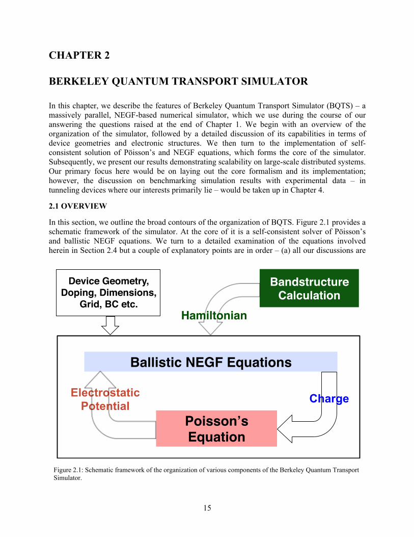
In this chapter, we describe the features of Berkeley Quantum Transport Simulator (BQTS) – a massively parallel, NEGF-based numerical simulator, which we use during the course of our answering the questions raised at the end of Chapter 1. We begin with an overview of the organization of the simulator, followed by a detailed discussion of its capabilities in terms of device geometries and electronic structures. We then turn to the implementation of self-consistent solution of Pöisson’s and NEGF equations, which forms the core of the simulator. Subsequently, we present our results demonstrating scalability on large-scale distributed systems. Our primary focus here would be on laying out the core formalism and its implementation; however, the discussion on benchmarking simulation results with experimental data – in tunneling devices where our interests primarily lie – would be taken up in Chapter 4.
2.1 OVERVIEW
In this section, we outline the broad contours of the organization of BQTS. Figure 2.1 provides a schematic framework of the simulator. At the core of it is a self-consistent solver of Pöisson’s and ballistic NEGF equations. We turn to a detailed examination of the equations involved herein in Section 2.4 but a couple of explanatory points are in order – (a) all our discussions are
Figure 2.1: Schematic framework of the organization of various components of the Berkeley Quantum Transport Simulator.
Charge Electrostatic
Potential
Poisson!s Equation"
Ballistic NEGF Equations"
Bandstructure Calculation"
Hamiltonian"
Device Geometry,
Doping, Dimensions,
Grid, BC etc."
16
confined to the SCF regime and the dimensions under consideration are large enough to ignore Coulomb blockade effects; (b) although even in short-channel-length devices there invariably exists some amount of scattering, we primarily focus on ballistic simulations due to the following reasons – (i) inclusion of scattering effects in a strict sense renders the calculations greatly computationally expensive by destroying the inherent parallelism present otherwise [1]; (ii) the best-case performance is a fairly good indicator of feasibility in case of several tunneling-related problems of our interest.
The Hamiltonian description of the system – an input to the core solver described above – comes through the band structure calculation module of the simulator. While the simulator can, in principle, handle any Hamiltonian represented in an orthogonal basis, we have been focusing on semi-empirical tight binding, k.p and effective mass descriptions so far – the details of which shall be described in section 2.3. In addition, various geometry-related parameters including grid-size, doping concentrations in different regions, electrical boundary conditions (BC) at the edges of the simulation domain etc. act as inputs to the simulator.
2.2 DEVICE STRUCTURES
This section will focus on describing the flexibility that BQTS provides in terms of incorporating various device structures and geometries. An important feature of the core-solver is its agnosticism to material-specific details. This means that the core of the simulator can be used to investigate electronic transport behavior in a wide range of materials – Si, Ge, InAs, GaN, graphene to name a few – without any modification. The dimensionality of the systems under investigation – from 1-D (e.g., nanowires, nanoribbons etc.) to 3-D (bulk semiconductors) – is also handled in a fairly generic manner. This requires a brief explanation – in order to accurately represent the device behavior, depending on the spatial variation of electrostatic potential, certain dimensions (along which the changes are rapid) need to be resolved in real-space while in some others (where the variation is slow or negligible) a periodic boundary condition could be imposed and hence a momentum-space representation suffices therein. The generality of the simulator implies that with a Hamiltonian with some of its dimensions represented in real-space and some others in momentum-space as input, the simulator can compute physical quantities of interest in a straightforward manner. We shall return to the discussion on the trade-offs of using real- and momentum-space representations in a later section. Another characteristic of the simulator is that in addition to being able to capture spatial variation in doping profiles, fixed charges arising due to traps and impurities, and dielectric interfaces, it can include, with the knowledge of each of the materials’ electronic structure- and electrostatics-related parameters, hetero-structures in the transport calculations. We also note that BQTS can handle both reflectionless, Ohmic (e.g., heavily doped semiconductors) and Schottky type of contacts in the self-consistent calculations thereby providing significant flexibility in exploring several of the novel material-systems wherein contacts are mainly of latter kind and where the issue of designing low-resistance contacts is an area of active research [2], [3].
2.3 ELECTRONIC STRUCTURE CAPABILITIES
In this section, we discuss the flexibilities offered by BQTS in terms of types of electronic structures that can be incorporated. The choice of right method to describe band structure depends on the specific problem at hand – computation-time and accuracy being the trade-off variables. While from a formalism viewpoint, NEGF can, in principle, work with a Hamiltonian
17
described in non-orthogonal bases as well, we confine ourselves to the orthogonal basis representations [4]. Specifically, we discuss, in some detail, our efforts in working with k.p and semi-empirical tight binding methods in our studies.
2.3.1 THE k.p METHOD
The k.p method for calculating the electronic structures has been used extensively over the last few decades in case of a wide range of semiconductors – most prominently in investigating optical properties of direct-bandgap semiconductors, heterostructures and quantum wells [5]. For a comprehensive elucidation of the approach, the readers are urged to peruse Refs. [6]-[8]. Here, however, we outline some key ideas for the purposes of completeness. The main advantage of this approach is fourfold – (a) it provides a reasonable compromise in terms of both time and model-complexity between simpler approaches like effective-mass Hamiltonian and more elaborate descriptions such as tight-binding and ab-initio methods; (b) the model parameters such as bandgap, effective mass, optical matrix elements etc. can be inferred easily from experiments and hence the method becomes an attractive option in case of new materials, for exploring their potential in initial feasibility studies before a more rigorous description could be used; (c) it provides a way to include effects of strain and spin-orbit interactions in a relatively straightforward manner; (d) it provides analytical expressions for band dispersions close to high-symmetry points in the Brillouin zone (BZ).
At the core of it, k.p method relies on perturbative expansion of the Bloch functions around certain point in the BZ (e.g., most commonly, zone center in case of zinc-blende III-V semiconductors). In terms of notations, denoting the wavefunction of a certain band indexed by n at a point
k in the BZ by
Ψn k ( r )(
= ei k . r u
n k ( r ), where
un k ( r ) denotes the periodic part of the
wavefunction), the single-particle Hamiltonian equation (
HΨn k ( r ) = En (
k )Ψ
n k ( r )) could be
written in terms of
un k ( r ) as –
(H0 + Hk + Hk.p )un k ( r ) = En (
k )u
n k ( r ) (1)
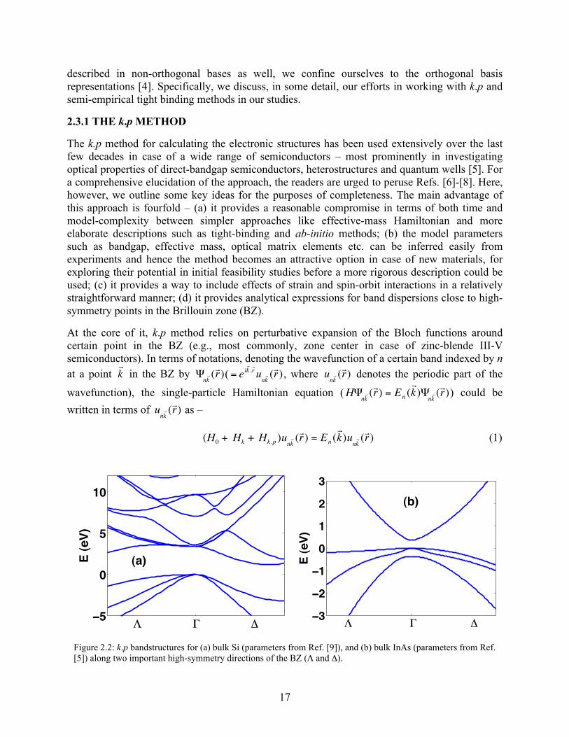
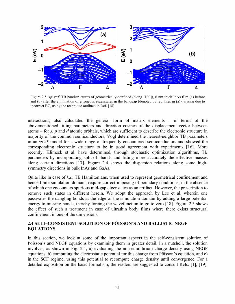
Figure 2.2: k.p bandstructures for (a) bulk Si (parameters from Ref. [9]), and (b) bulk InAs (parameters from Ref. [5]) along two important high-symmetry directions of the BZ (Λ and Δ).
5
0
5
10
E (e
V)
(a)
3
2
1
0
1
2
3
E (e
V)
(b)
18
where H0 is the unperturbed Hamiltonian (i.e., at
k = 0),
Hk =2 k 2
2m, and
Hk.p =m k . p (with
,
m and
p being the reduced Planck’s constant, free electron mass and momentum operator respectively). Now,
un k ( r ) can be expanded in an orthonormal basis of Bloch functions at a
high-symmetry point, e.g., for expansion around
k = Γ,
un k ( r ) = a j (
j =1
N
∑ k )u j0(
r ) (2)
The total number of bands, N, generally used depends both on the material in question and the problem at hand – 6 bands are sufficient to describe the valence bands of zinc-blende (ZB) III-Vs with the inclusion of spin-orbit interaction, 2 more bands for incorporating conduction band description; 15 bands to describe the indirect bandgap in case of Si, Ge etc [5], [9]. The number of parameters required to uniquely determine the bandstructure is governed by the inherent symmetries of the BZ. We note that the accuracy of the resulting eigenfunctions and eigenvalues progressively decreases as
k increases. Non-parabolic effects like valence-band warping can be
taken care of by increasing the order of perturbation. Of particular interest are the commonly used Luttinger-Kohn (LK) and Dresselhaus-Kip-Kittel (DKK) Hamiltonians in the description of valence bands of ZB semiconductors whose second-order-perturbation model-parameters depend on Luttinger parameters that are very well-known for most materials of interest [10], [11]. The said parameters are fitted, in most cases, to obtain an accurate electronic structure description in bulk semiconductors. The illustration of the method in calculating dispersion relations in InAs and silicon – two of the most common semiconductors – along a couple of high-symmetry directions is shown in Fig. 2.2.
A couple of important points must be noted here – (a) as discussed in Section 2.2, in most transport calculations, some directions require a real-space representation of the electronic
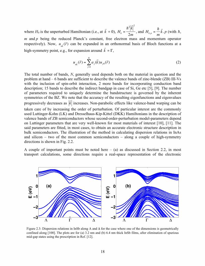
Figure 2.3: Dispersion relations in InSb along Λ and Δ for the case where one of the dimensions is geometrically confined along [100]. The plots are for (a) 3.2 nm and (b) 6.4 nm thick InSb films, after elimination of spurious mid-gap states using the prescription in Ref. [12].
3
2
1
0
1
E (e
V)
(a)
3
2
1
0
1
E (e
V)
(b)
19
structure. A straightforward prescription of translating to such a representation from the momentum-space representation is by noting that the projection of
k in position-space is given
by –
k ↔ −i∇, the gradient operator, and projecting this onto a finite-difference grid. The grid-
spacing herein should be chosen such that with a finite N-band representation there should exist appropriate density-of-states (DOS) within the energy range of interest while simultaneously ensuring that it is not too small as to reach large values of
k where the accuracy of the method
reduces; (b) in certain nanostructures, there exists geometrical confinement along certain dimensions and abruptly terminating the real-space Hamiltonian in the simulation domain in such cases leads to incorrect imposing of boundary conditions and hence spurious eigenvalue solutions in the bandgap. Hence care must be taken in order to ensure elimination of such artifacts through modification of model-parameters. In this regard, a subtle point is in order: the abovementioned spurious states might be manifested in certain non-symmetric direction and hence examining the bandstructure along high-symmetry lines of BZ will not suffice. A robust test is to plot the transmission probability (discussed later in Section 2.4.2), where contributions from eigenstates corresponding to all momenta at a given energy are accounted for. We use the solution proposed by Foreman by analyzing the roots of secular equation to get rid of incorrect solutions [12] (Fig. 2.3). In the next subsection, we discuss in detail the semi-empirical tight-binding method for describing electronic structure.
2.3.2 THE SEMI-EMPIRICAL TIGHT-BINDING METHOD
In this section, we would like to discuss briefly certain aspects related to using tight-binding based Hamiltonians in our simulations. Tight-binding (TB) methods provide more elaborate descriptions of electronic structure in solids than the k.p-based methods. Hence their accuracy is better, albeit at the expense of increased computational burden. However, they are less accurate than the more comprehensive but computation-intensive density-functional theory, from which the former can be derived under certain approximations [13]. While TB approach comes in both orthogonal- and non-orthogonal-bases flavors, we confine our discussions herein to the former due to their simplicity of incorporation in electronic transport calculations.
Unlike in case of k.p method where the basis functions were defined on a unit cell (or a finite-difference grid), TB method relies on expansion of the electronic wavefunction as a linear combination of atomic orbitals (LCAO) that constitute the crystal. This emanates from the assumption that the single-particle, time-independent Hamiltonian of the crystal could be written as a sum of isolated atomic Hamiltonian and some overlapping potential due to the presence of neighboring atoms in the crystal lattice, i.e.,
H( r ) = Hatom ( R n
∑ r − R n ) + V ( r ) (3)
where the summation extends over all atomic sites in the lattice
R n and
V ( r ) is the correction to the isolated atomic potential. Assuming that the effect of
V ( r ) is only in altering the isolated-atom electronic wavefunction only in a perturbative sense, the eigenfunctions of
H( r ) could be written as a linear combination of the former, i.e.,
ψ( r ) = am (m, R n
∑ R n )ψm ( r −
R n ) (4)
20
where
ψm denotes the wavefunction corresponding to m-th atomic orbital. Imposing the translational symmetry of the crystal through the Bloch’s theorem, the coefficients am satisfy the family of equations –
am ( R n −
R t ) = ei
k .( R n −
R t )am (
0 ) (5)
for all translational vectors of the lattice
R t . In orthogonal TB, one uses modified orbitals –
obtained by Löwdin orthonormalization of atomic orbitals – such that wavefunctions corresponding to different atomic sites are orthogonal [14]. In such a case, the wavefunction could be written, in terms of orthogonalized Löwdin orbitals,
Ψm , as –
ψ( r ) =1N
ei k . R n
m, R n
∑ Ψm ( r − R n ) (6)
where N is the number of atoms in the lattice. It is easy to notice that with (6) as an eigenfunction, finding the eigenvalues of
H( r ) involves computation of overlap integrals of
V ( r ) , typically for large number of
R n , thus making them difficult to evaluate. However, Slater
and Koster noted that although analytical evaluation of those terms is practically infeasible, since the wavefunctions and eigenvalues have the correct symmetry properties, it is possible to get accurate bandstructure description at any point in the BZ as long as the approximations preserve the symmetry dictated by the crystal structure [15]. In particular, they suggested using some of the integrals as fitting parameters, which are to be chosen such that the energies thus calculated agree well with those determined either through experiments or through more precise electronic structure calculation methods at certain high symmetry points in the BZ. Also, another simplifying assumption is the neglecting of three-center integrals – arising in calculation of matrix elements of
H( r ) due to periodic atomic potential i.e.,
Ψm* ( r −
R i)Vatom (∫ r −
R k )Ψn (
r − R j )dv – in comparison to two-center integrals (i.e., k = i or k =
j). Slater and Koster, noting that this approach necessitates the use of only few nearest-neighbor
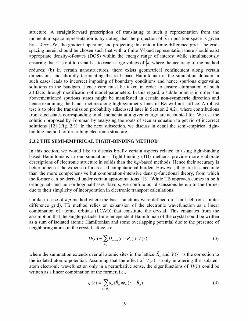
Figure 2.4: Semi-empirical TB bandstructures of (a) bulk GaAs and (b) bulk InAs using an sp3s*d5 set of basis functions. The parameters used herein are obtained from Ref. [17].
2
1
0
1
2
3
E (e
V) (a)
2
1
0
1
2
3
E (e
V) (b)
21
interactions, also calculated the general form of matrix elements – in terms of the abovementioned fitting parameters and direction cosines of the displacement vector between atoms – for s, p and d atomic orbitals, which are sufficient to describe the electronic structure in majority of the common semiconductors. Vogl determined the nearest-neighbor TB parameters in an sp3s* model for a wide range of frequently encountered semiconductors and showed the corresponding electronic structure to be in good agreement with experiments [16]. More recently, Klimeck et al. have determined, through stochastic optimization algorithms, TB parameters by incorporating split-off bands and fitting more accurately the effective masses along certain directions [17]. Figure 2.4 shows the dispersion relations along some high-symmetry directions in bulk InAs and GaAs.
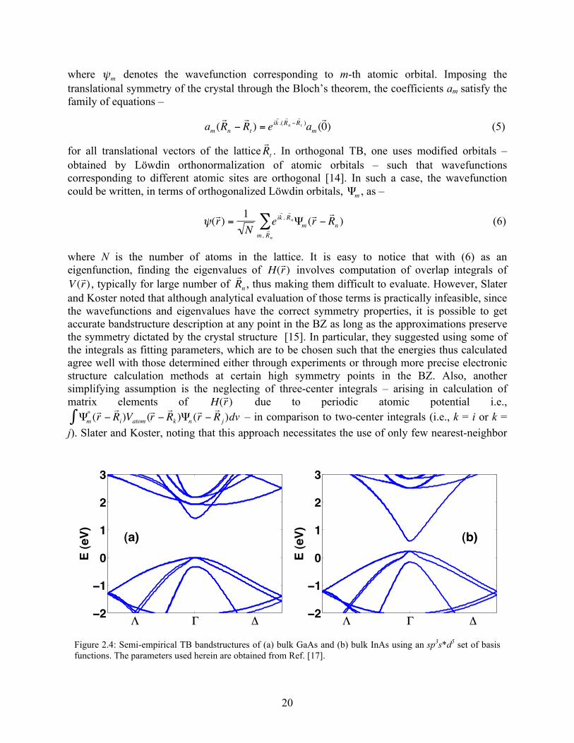
Quite like in case of k.p, TB Hamiltonians, when used to represent geometrical confinement and hence finite simulation domain, require correct imposing of boundary conditions, in the absence of which one encounters spurious mid-gap eigenstates as an artifact. However, the prescription to remove such states in different herein. We adopt the approach by Lee et al. wherein one passivates the dangling bonds at the edge of the simulation domain by adding a large potential energy to missing bonds, thereby forcing the wavefunction to go to zero [18]. Figure 2.5 shows the effect of such a treatment in case of ultrathin body films where there exists structural confinement in one of the dimensions.
2.4 SELF-CONSISTENT SOLUTION OF PÖISSON’S AND BALLISTIC NEGF EQUATIONS
In this section, we look at some of the important aspects in the self-consistent solution of Pöisson’s and NEGF equations by examining them in greater detail. In a nutshell, the solution involves, as shown in Fig. 2.1, a) evaluating the non-equilibrium charge density using NEGF equations, b) computing the electrostatic potential for this charge from Pöisson’s equation, and c) in the SCF regime, using this potential to recompute charge density until convergence. For a detailed exposition on the basic formalism, the readers are suggested to consult Refs. [1], [19].
Figure 2.5: sp3s*d5 TB bandstructures of geometrically-confined (along [100]), 6 nm thick InAs film (a) before and (b) after the elimination of erroneous eigenstates in the bandgap (denoted by red lines in (a)), arising due to incorrect BC, using the technique outlined in Ref. [18].
2
1
0
1
2
E (e
V)(a)
2
1
0
1
2
3
E (e
V) (b)
22
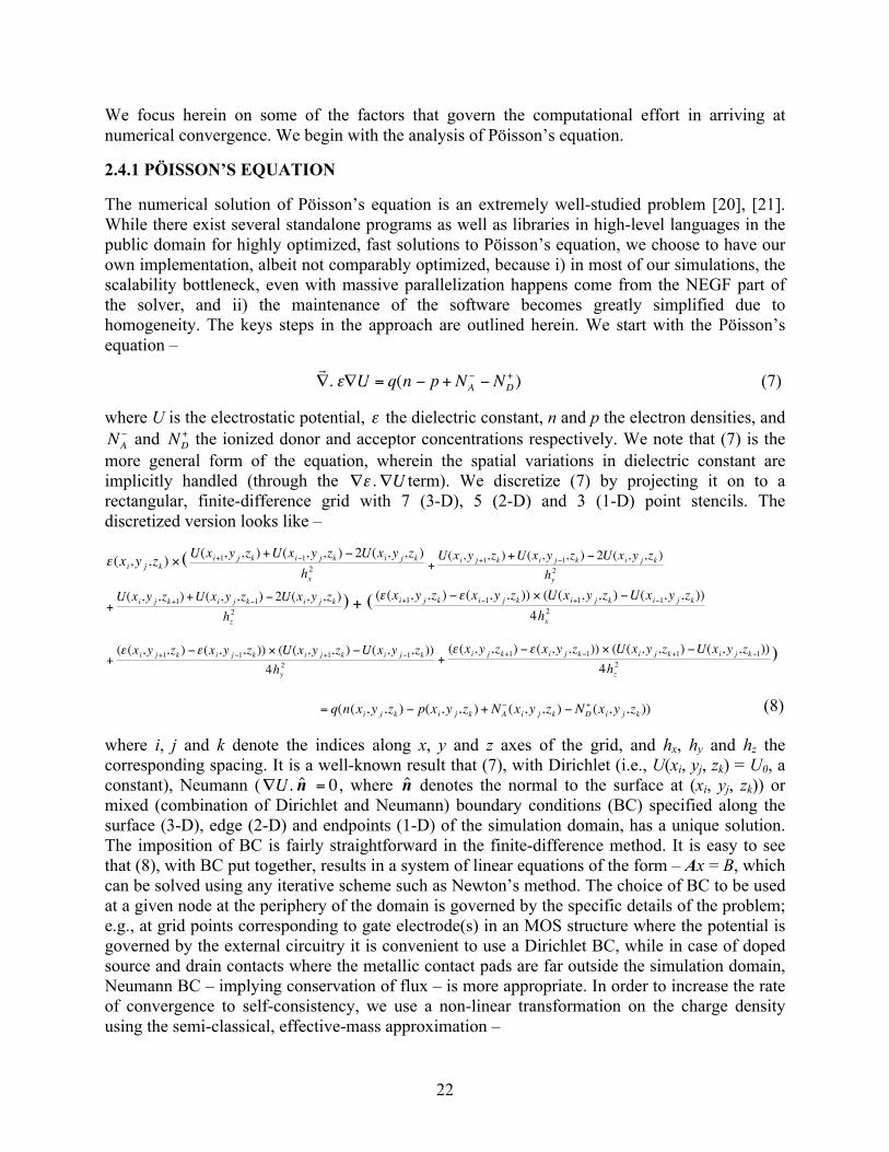
We focus herein on some of the factors that govern the computational effort in arriving at numerical convergence. We begin with the analysis of Pöisson’s equation.
2.4.1 PÖISSON’S EQUATION
The numerical solution of Pöisson’s equation is an extremely well-studied problem [20], [21]. While there exist several standalone programs as well as libraries in high-level languages in the public domain for highly optimized, fast solutions to Pöisson’s equation, we choose to have our own implementation, albeit not comparably optimized, because i) in most of our simulations, the scalability bottleneck, even with massive parallelization happens come from the NEGF part of the solver, and ii) the maintenance of the software becomes greatly simplified due to homogeneity. The keys steps in the approach are outlined herein. We start with the Pöisson’s equation –
∇ . ε∇U = q(n − p + NA
− − ND+ ) (7)
where U is the electrostatic potential,
ε the dielectric constant, n and p the electron densities, and
NA− and
ND+ the ionized donor and acceptor concentrations respectively. We note that (7) is the
more general form of the equation, wherein the spatial variations in dielectric constant are implicitly handled (through the
∇ε . ∇U term). We discretize (7) by projecting it on to a rectangular, finite-difference grid with 7 (3-D), 5 (2-D) and 3 (1-D) point stencils. The discretized version looks like –
ε(xi,y j ,zk ) × (
U(xi+1,y j ,zk ) +U(xi−1,y j ,zk ) − 2U(xi,y j ,zk )hx2
+U(xi,y j+1,zk ) +U(xi,y j−1,zk ) − 2U(xi,y j ,zk )
hy2
+U(xi,y j ,zk+1) +U(xi,y j ,zk−1) − 2U(xi,y j ,zk )
hz2
) ++ (
(ε (xi+1,y j ,zk ) −ε(xi−1,y j ,zk )) × (U(xi+1,y j ,zk ) −U(xi−1,y j ,zk ))4hx
2
+(ε (xi,y j+1,zk ) −ε(xi,y j−1,zk )) × (U(xi,y j+1,zk ) −U(xi,y j−1,zk ))
4hy2
+(ε (xi,y j ,zk+1) −ε(xi,y j ,zk−1)) × (U(xi,y j ,zk+1) −U(xi,y j ,zk−1))
4hz2
)
= q(n(xi,y j ,zk ) − p(xi,y j ,zk ) + NA− (xi,y j ,zk ) − ND
+ (xi,y j ,zk )) (8)
where i, j and k denote the indices along x, y and z axes of the grid, and hx, hy and hz the corresponding spacing. It is a well-known result that (7), with Dirichlet (i.e., U(xi, yj, zk) = U0, a constant), Neumann (
∇U. ˆ n = 0 , where
ˆ n denotes the normal to the surface at (xi, yj, zk)) or mixed (combination of Dirichlet and Neumann) boundary conditions (BC) specified along the surface (3-D), edge (2-D) and endpoints (1-D) of the simulation domain, has a unique solution. The imposition of BC is fairly straightforward in the finite-difference method. It is easy to see that (8), with BC put together, results in a system of linear equations of the form – Ax = B, which can be solved using any iterative scheme such as Newton’s method. The choice of BC to be used at a given node at the periphery of the domain is governed by the specific details of the problem; e.g., at grid points corresponding to gate electrode(s) in an MOS structure where the potential is governed by the external circuitry it is convenient to use a Dirichlet BC, while in case of doped source and drain contacts where the metallic contact pads are far outside the simulation domain, Neumann BC – implying conservation of flux – is more appropriate. In order to increase the rate of convergence to self-consistency, we use a non-linear transformation on the charge density using the semi-classical, effective-mass approximation –
23
n = NcF1/ 2Fn − Ec,old
kBT⎛
⎝ ⎜
⎞
⎠ ⎟ (9)
p = NvF1/ 2Ev,old − Fp
kBT⎛
⎝ ⎜
⎞
⎠ ⎟ (10)
where
Ec,old and
Ev,old are the conduction and valence band energies from the previous iteration of self-consistency inferred from
Uold , Nc and Nv the corresponding effective density-of-states (DOS), F1/2 the Fermi-Dirac integral of order ½, kB the Boltzmann constant and T the temperature. We have dropped the arguments (xi, yj, zk) in (9) and (10) for clarity. We note that the above equations are only to improve the convergence rate and the assumptions therein have no bearing on the resulting self-consistent charge densities and electrostatic potential profiles as the former quantities are calculated solely from NEGF equations. A weighted average of electrostatic potential from the previous iteration and new solution from Pöisson’s equation as the new potential ensures that the convergence to self-consistency is smooth. The weights could be tuned based on the difference between new and old values.
2.4.2 BALLISTIC NEGF EQUATIONS
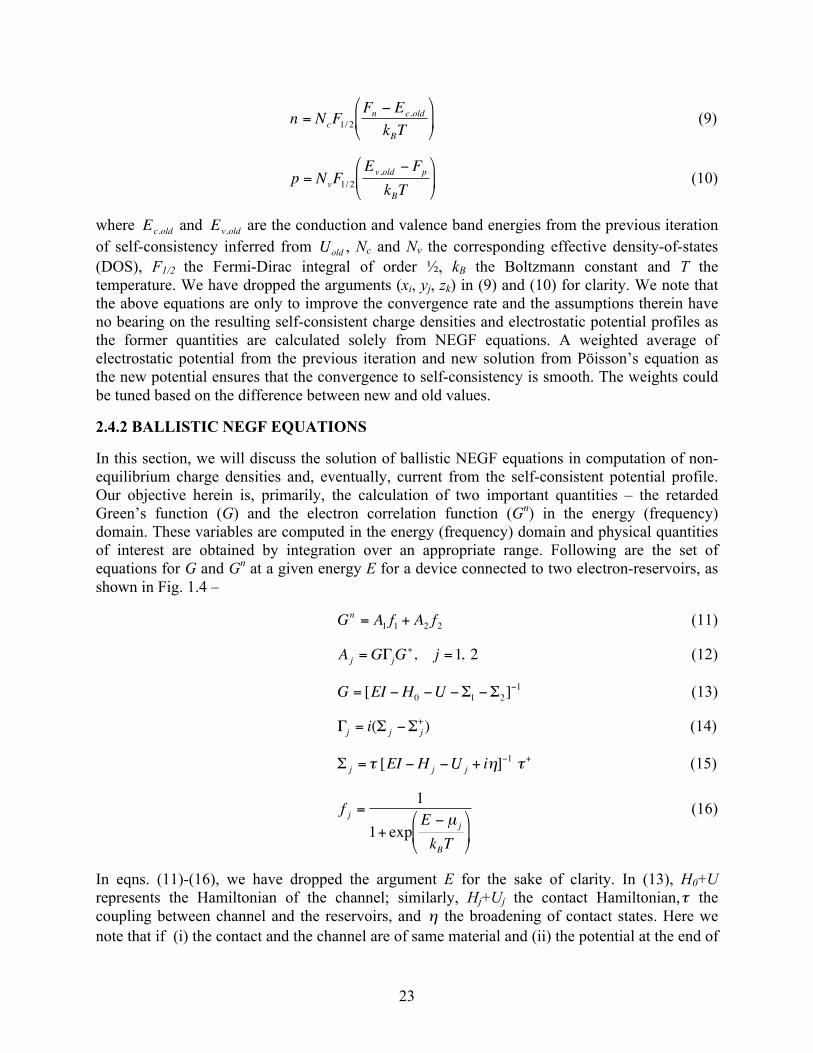
In this section, we will discuss the solution of ballistic NEGF equations in computation of non-equilibrium charge densities and, eventually, current from the self-consistent potential profile. Our objective herein is, primarily, the calculation of two important quantities – the retarded Green’s function (G) and the electron correlation function (Gn) in the energy (frequency) domain. These variables are computed in the energy (frequency) domain and physical quantities of interest are obtained by integration over an appropriate range. Following are the set of equations for G and Gn at a given energy E for a device connected to two electron-reservoirs, as shown in Fig. 1.4 –
Gn = A1 f1 + A2 f2 (11)
A j =GΓjG+, j =1, 2 (12)
G = [EI −H0 −U −Σ1 −Σ2]−1 (13)
Γj = i(Σ j −Σ j+) (14)
Σ j = τ [EI −H j −U j + iη]−1 τ + (15)
f j =1
1+ expE − µ j
kBT⎛
⎝ ⎜
⎞
⎠ ⎟
(16)
In eqns. (11)-(16), we have dropped the argument E for the sake of clarity. In (13), H0+U represents the Hamiltonian of the channel; similarly, Hj+Uj the contact Hamiltonian,
τ the coupling between channel and the reservoirs, and
η the broadening of contact states. Here we note that if (i) the contact and the channel are of same material and (ii) the potential at the end of
24
the channel and in the contact are identical, it then corresponds to the case of reflection-less contacts i.e., there would be no momentum mismatch for carriers moving between contact and channel. The case of dissimilar materials and band-offsets at the channel/contact interface – as is customary in Schottky barrier devices – is more difficult to handle. An appropriate way to deal with this situation is through incorporation of some finite region of the contact (typically about 3-5 layers) into the extended channel regime, beyond which a regular self-energy description, calculated using the contact-metal Hamiltonian, suffices.
The charge densities (ρ) and current (I) can be calculated as –
ρ =12π
GndE∫ (17)
I =qh
Trace(Γ1GΓ2G+)( f1 − f2)dE∫ (18)
where h denotes the Planck’s constant. A few points need emphasis here – i) in (17), we are concerned with the diagonal elements of Gn in computing spatially resolved densities; ii) also, the range of integration is determined on whether the charge density corresponds to electron or hole concentration – the former is calculated for conduction band states, i.e., from bottom of the conduction band and the latter for valence band states, in which case the variable is the hole correlation function, Gp, (= A1+A2 - Gn) instead of Gn; iii) the volume charge density to be used in (8) is obtained by summing ρ over the orbitals/bands and dividing it by the volume of the unit grid (k.p) or unit cell (TB) under consideration; iv) in all our simulations, we have kept the spatial grid for NEGF and Pöisson’s equations to be identical; this is not a necessity and if they are chosen to be different, interpolation/extrapolation methods could be used to translate from one to another. v) In the Green’s function formalism, the trace term in (18) represents the transmission coefficient, which for in a mesoscopic-physics parlance, is the total transmission (of probability flux) by taking into account all modes at a given energy E.
The computational challenges of equations (11)-(16) are easy to appreciate. The task of computing Green’s function G, for a device with even a few hundreds of atoms – each represented with around 10-20 atomic orbitals as in case of TB – is unwieldy if done through explicit inversion of matrices, as (13) indicates. An even bigger challenge arises if self-energies need to be calculated by inverting the matrices containing the contact Hamiltonian, as the reservoirs are, in general, much bigger in size than the channel. We shall discuss solutions to circumvent these problems, arising due to inversion of large matrices, in the ensuing paragraphs.
Computing self-energies could be done through calculation of surface Green’s functions for the reservoirs (g) – by operating on much smaller matrices – since the self-energy matrices would be non-zero only for those blocks where contact connects to the channel i.e., only where
τ is non-zero. With g computed, the relevant block is calculated as
˜ τ g ˜ τ +, where
˜ τ is the non-zero block of
τ . However, an iterative solution – required to compute g – has a very slow convergence rate. A better way to compute the same is by a method involving replacement of layered chain of atoms in the contact with progressively bigger (with larger lattice constant) effective chains, proposed by Sancho et al. [22].
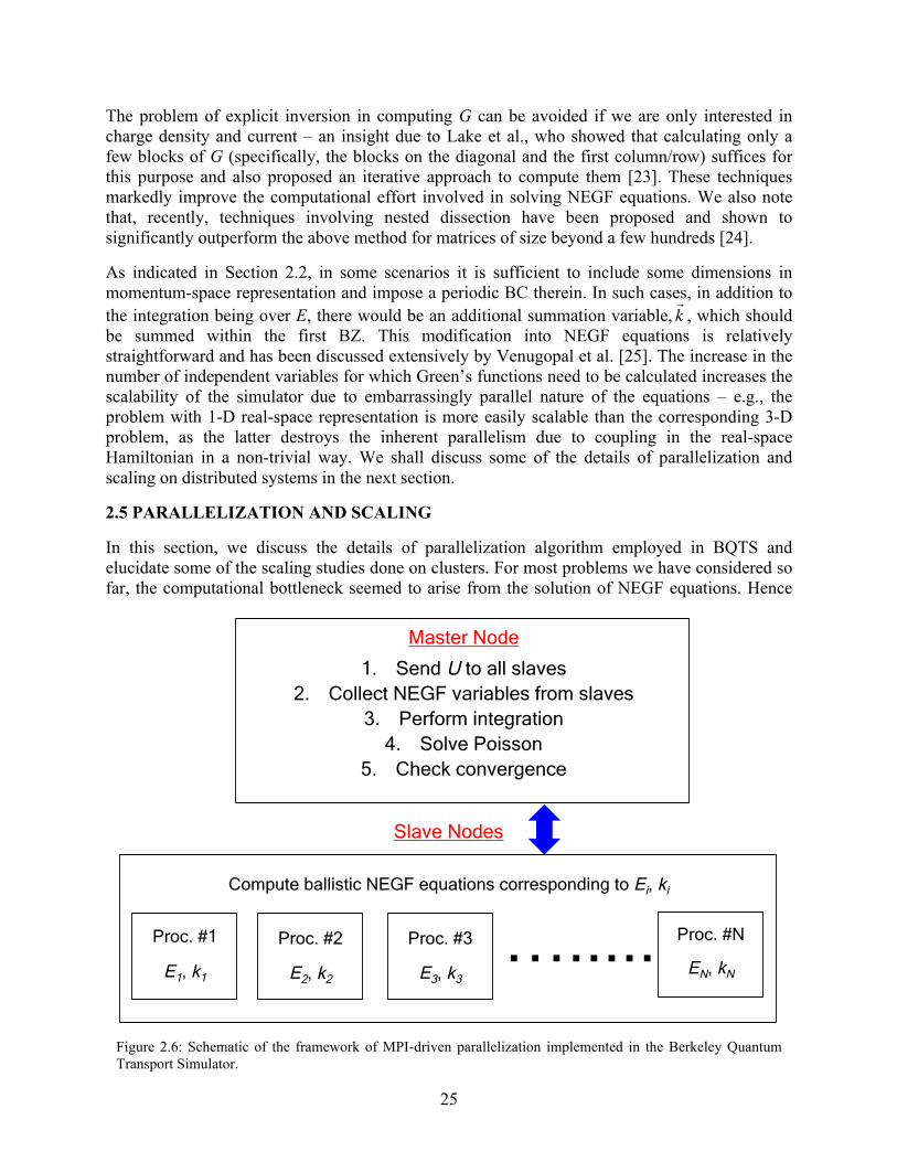
25
The problem of explicit inversion in computing G can be avoided if we are only interested in charge density and current – an insight due to Lake et al., who showed that calculating only a few blocks of G (specifically, the blocks on the diagonal and the first column/row) suffices for this purpose and also proposed an iterative approach to compute them [23]. These techniques markedly improve the computational effort involved in solving NEGF equations. We also note that, recently, techniques involving nested dissection have been proposed and shown to significantly outperform the above method for matrices of size beyond a few hundreds [24].
As indicated in Section 2.2, in some scenarios it is sufficient to include some dimensions in momentum-space representation and impose a periodic BC therein. In such cases, in addition to the integration being over E, there would be an additional summation variable,
k , which should
be summed within the first BZ. This modification into NEGF equations is relatively straightforward and has been discussed extensively by Venugopal et al. [25]. The increase in the number of independent variables for which Green’s functions need to be calculated increases the scalability of the simulator due to embarrassingly parallel nature of the equations – e.g., the problem with 1-D real-space representation is more easily scalable than the corresponding 3-D problem, as the latter destroys the inherent parallelism due to coupling in the real-space Hamiltonian in a non-trivial way. We shall discuss some of the details of parallelization and scaling on distributed systems in the next section.
2.5 PARALLELIZATION AND SCALING
In this section, we discuss the details of parallelization algorithm employed in BQTS and elucidate some of the scaling studies done on clusters. For most problems we have considered so far, the computational bottleneck seemed to arise from the solution of NEGF equations. Hence
Figure 2.6: Schematic of the framework of MPI-driven parallelization implemented in the Berkeley Quantum Transport Simulator.
Proc. #1 Proc. #2 Proc. #3 Proc. #N
E1, k1 E2, k2 E3, k3 EN, kN
Master Node
1. Send U to all slaves 2. Collect NEGF variables from slaves
3. Perform integration 4. Solve Poisson
5. Check convergence
Compute ballistic NEGF equations corresponding to Ei, ki
….....
Slave Nodes
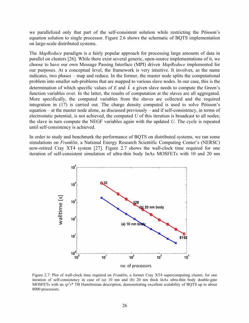
26
we parallelized only that part of the self-consistent solution while restricting the Pöisson’s equation solution to single processor. Figure 2.6 shows the schematic of BQTS implementation on large-scale distributed systems.
The MapReduce paradigm is a fairly popular approach for processing large amounts of data in parallel on clusters [26]. While there exist several generic, open-source implementations of it, we choose to have our own Message Passing Interface (MPI) driven MapReduce implemented for our purposes. At a conceptual level, the framework is very intuitive. It involves, as the name indicates, two phases – map and reduce. In the former, the master node splits the computational problem into smaller sub-problems that are mapped to various slave nodes. In our case, this is the determination of which specific values of E and
k a given slave needs to compute the Green’s
function variables over. In the latter, the results of computation at the slaves are all aggregated. More specifically, the computed variables from the slaves are collected and the required integration in (17) is carried out. The charge density computed is used to solve Pöisson’s equation – at the master node alone, as discussed previously – and if self-consistency, in terms of electrostatic potential, is not achieved, the computed U of this iteration is broadcast to all nodes; the slave in turn compute the NEGF variables again with the updated U. The cycle is repeated until self-consistency is achieved.
In order to study and benchmark the performance of BQTS on distributed systems, we ran some simulations on Franklin, a National Energy Research Scientific Computing Center’s (NERSC) now-retired Cray XT4 system [27]. Figure 2.7 shows the wall-clock time required for one iteration of self-consistent simulation of ultra-thin body InAs MOSFETs with 10 and 20 nm
Figure 2.7: Plot of wall-clock time required on Franklin, a former Cray XT4 supercomputing cluster, for one iteration of self-consistency in case of (a) 10 nm and (b) 20 nm thick InAs ultra-thin body double-gate MOSFETs with an sp3s* TB Hamiltonian description, demonstrating excellent scalability of BQTS up to about 8000 processors.

27
thicknesses, described by a sp3s* TB Hamiltonian. We observe a near-perfect scaling up to 8192 processors, thus demonstrating very good scalability.
We conclude this chapter after having discussed several of the implementation-related issues of Berkeley Quantum Transport Simulator. In the next chapter, we start with some results obtained using the same. Before moving on to the tunneling problem, which will be our primary interest, we perform some studies on a simpler system – two-dimensional channel MOSFET with an effective mass Hamiltonian description – to ascertain the correctness of our simulations while simultaneously investigating the suitability of a fairly new 2-D system for low-power applications.
2.6 REFERENCES
[1] S. Datta, “Quantum transport: atom to transistor,” Cambridge University Press, 2005.
[2] F. Schwierz, “Graphene transistors,” Nat. Nanotechnol., vol. 5, no. 7, pp. 487-496, 2010.
[3] I. Popov, G. Seifert, and D. Tománek, “Designing Electrical Contacts to MoS2 Monolayers: A Computational Study,” Phys. Rev. Lett., vol. 108, no. 15, pp. 156802-156806, 2012.
[4] F. Zahid, M. Paulsson, and S. Datta, “Electrical Conduction through Molecules,” in Advanced Semiconductors and Organic Nano-Techniques, H. Morkoc, Ed. San Diego: Academic Press, 2003, pp. 1-41.
[5] D. Gershoni, C. H. Henry, G. A. Baraff, “Calculating the Optical Properties of Multidimensional Heterostructures: Application to the Modeling of Quaternary Quantum Well Lasers,” IEEE J. Quantum Elect., vol. 29, no. 9, pp. 2433-2450, 1993.
[6] P. Yu and M. Cardona, “Fundamentals of Semiconductors: Physics and Materials Properties,” Springer, 2010.
[7] L. C. Lew Yan Voon and M. Willatzen, “The k-p Method: Electronic Properties of Semiconductors,” Springer, 2009.
[8] J. Singh, “Electronic and Optoelectronic Properties of Semiconductor Structures,” Cambridge University Press, 2007.
[9] M. Cardona and F. H. Pollak, “Energy-Band Structure of Germanium and Silicon: The k·p Method,” Phys. Rev., vol. 142, no. 2, pp. 530-543, 1966.
[10] J. M. Luttinger, and W. Kohn, “Motion of Electrons and Holes in Perturbed Periodic Fields,” Phys. Rev., vol. 97, no. 4, pp. 869-883, 1955.
[11] G. Dresselhaus, A. F. Kip, and C. Kittel, “Cyclotron Resonance of Electrons and Holes in Silicon and Germanium Crystals,” Phys. Rev., vol. 98, no. 2, pp. 368-384, 1955.
[12] B. A. Foreman, “Elimination of spurious solutions from eight-band k.p theory,” Phys. Rev. B, vol. 56, no. 20, pp. R12748–R12751, 1997.
[13] W. M. C. Foulkes, and R. Haydock, “Tight-binding models and density-functional theory,” Phys. Rev. B, vol. 39, no. 17, pp. 12520-12536, 1989.
28
[14] P. Löwdin, “On the Non‐Orthogonality Problem Connected with the Use of Atomic Wave Functions in the Theory of Molecules and Crystals,” J. Chem. Phys., vol. 18, no. 3, pp. 365-375, 1950.
[15] J. C. Slater and G. F. Koster, “Simplified LCAO Method for the Periodic Potential Problem,” Phys. Rev., vol. 94, no. 6, pp. 1498-1524, 1954.
[16] P. Vogl, H. P. Hjalmarson and J. D. Dow, “A Semi-empirical tight-binding theory of the electronic structure of semiconductors,” J. Phys. Chem. Solids, vol. 44, no. 5, pp. 365-378, 1983.
[17] G. Klimeck, F. Oyafuso, T. B. Boykin, R. C. Bowen and P. von Allmen, “Development of a Nanoelectronic 3-D (NEMO 3-D) Simulator for Multimillion Atom Simulations and Its Application to Alloyed Quantum Dots,” CMES - Comp. Model Eng., vol. 3, no. 5, pp. 601-642, 2002.
[18] S. Lee, F. Oyafuso, P. von Allmen, and G. Klimeck, “Boundary conditions for the electronic -extent embedded semiconductor nanostructures,” Phys. Rev. B, vol. 69, no. 4,
pp. 045316-045323, 2004.
[19] M. P. Anantram, M. S. Lundstrom, and D. E. Nikonov, “Modeling of Nanoscale Devices,” Proc. IEEE, vol. 96, no. 9, pp. 1511-1550, 2008.
[20] S. Balay, J. Brown, K. Buschelman, W. D. Gropp, D. Kaushik, M. G. Knepley, L. C. McInnes, B. F. Smith, and H. Zhang, “PETSc Web page,” [online] 2013, http://www.mcs.anl.gov/petsc/ (Accessed: 10 September 2013).
[21] A. Logg, K. -A. Mardal, G. N. Wells, “Automated Solution of Differential Equations by the Finite Element Method – FEniCS Project”, [online] 2013, http://fenicsproject.org/ (Accessed: 10 September 2013).
[22] M. P. López Sancho, J. M. López Sancho and J. Rubio, “Highly convergent schemes for the calculation of bulk and surface Green functions,” J. Phys. F: Met. Phys., vol. 15, no. 4, pp. 851-858, 1985.
[23] R. Lake, G. Klimeck, R. C. Bowen, and D. Jovanovic, “Single and multiband modeling of quantum electron transport through layered semiconductor devices,” J. Appl. Phys., vol. 81, no. 12, pp. 7845-7869, 1997.
[24] U. Hetmaniuk, Y. Zhao, M. P. Anantram, “A Nested Dissection Approach to Modeling Transport in Nanodevices: Algorithms and Applications,” arXiv:1305.1070v1, 2013.
[25] R. Venugopal, Z. Ren, S. Datta, M. S. Lundstrom, and D. Jovanovic, “Simulating quantum transport in nanoscale transistors: Real versus mode-space approaches,” J. Appl. Phys., vol. 92, no. 7, pp. 3730-3739, 2002.
[26] J. Dean and S. Ghemawat, “MapReduce: Simplified Data Processing on Large Clusters,” Commun. ACM, vol. 51, no. 1, pp. 107-113, 2008.

29
[27] Franklin, NERSC’s Cray XT4 System, NERSC Powering Scientific Discovery Since 1974, [online] 2013, http://www.nersc.gov/users/computational-systems/retired-systems/franklin/ (Accessed: 10 September 2013).

30
CHAPTER 3
MOSFET SIMULATIONS – MONOLAYER MOLYBDENUM DISULFIDE TRANSISTORS AS EXEMPLARS
In Chapter 2, we laid out the details of the self-consistent NEGF formalism implemented in Berkeley Quantum Transport Simulator. The purpose of this chapter is twofold: a) while for the most part of the remainder of this thesis, we would be focusing on tunneling – be it in two-terminal or three-terminal devices – evaluating the simulator-behavior with a simpler system with relatively simpler physics serves the purpose of gaining confidence in moving into more complex scenarios where our intuitions have limited reach. We do this by investigating various results obtained from BQTS in case of MOSFET simulations – transfer, output and capacitance characteristics to name a few. b) By examining short-channel monolayer MoS2 transistors – a relatively new material-system gaining significant interest in recent years due to its two-dimensionality and finite bandgap – we identify their opportunities and challenges in being next-generation solutions for low-power applications.
3.1 MOLYBDENUM DISULFIDE
3.1.1 MATERIAL PROPERTIES
Molybdenum disulfide (MoS2), a layered transition metal dichalcogenide, has several interesting electrical, mechanical and optical properties [1]. Apart from being widely used as a dry lubricant for automobiles due to its low friction properties, MoS2 has been explored for applications in photovoltaics and photocatalysis for energy conversion [2]-[4]. Structurally, MoS2 is a stack of planes where covalently bonded S-Mo-S atoms are closely packed in a hexagonal arrangement (Fig. 3.1(a)), and the adjacent planes are held together by Van der Waals interactions [5]. These weak interlayer interactions, in contrast to strong intralayer bonding, make synthesis of monolayers of MoS2 possible by micromechanical exfoliation from bulk crystalline MoS2 [5]-[7] – identical to the fabrication of graphene from graphite [8]. Recent experimental studies on few layers of MoS2 using optical absorption and photoluminescence show that, while bulk MoS2 is an indirect bandgap semiconductor with a bandgap (EG) of 1.29 eV [9], at monolayer thickness
Figure 3.1: Atomistic configuration of MoS2 monolayer, showing the in-plane hexagonal arrangement. The S-Mo-S atoms form a trigonal prismatic structure. The monolayer is 6.5 Å thick.

31
(0.65 nm) [10], MoS2 transitions to a direct bandgap semiconductor with EG = 1.8 eV [5], [6], thereby corroborating earlier ab-initio based calculations that predicted a similar bandgap [11]. High thermal stability of MoS2 and the absence of dangling bonds [7], coupled with the presence of significant bandgap in a 2-D material render monolayer MoS2 as an attractive candidate for switching applications, unlike graphene where the absence of bandgap inhibits its use in spite of large reported mobilities (200,000 cm2/V-s) [12].
3.1.2 TRANSISTORS OF MONOLAYERS
While monolayer MoS2 has previously exhibited poor mobility (<10 cm2/V-s) [8] limiting its potential for majority of the electronic applications, it has been recently reported that in the presence of a high-κ environment, the mobility of monolayer MoS2 can increase by several times (~200 cm2/V-s) [7], which is similar to earlier reports of such phenomenon in case of graphene [13]. This mobility enhancement, one of the reasons of which could be dielectric screening as predicted by the theoretical calculations [14], opens up the possibility of monolayer MoS2 field-effect transistors for low standby and low operating power electronics. Recently, long channel monolayer MoS2 transistors with very good ON-OFF current ratio (>107) and subthreshold swing (74 mV/decade) have been demonstrated experimentally [7]. While rapid progress in fabrication of short-channel MoS2 transistors can be expected, it is of significant technological relevance to estimate the ultimate performance limit that can be achieved in such devices before an aggressive pursuit of miniaturization begins. We attempt to answer this question by using rigorous quantum transport simulations and view their performance in light of some of the competing non-silicon technologies to assess the viability of monolayer MoS2 transistors for future electronic applications.
3.2 SHORT-CHANNEL MOSFET SIMULATIONS
In this section, we begin with the extraction of some of the relevant physical parameters –required for our ballistic NEGF simulations and for their subsequent extrapolation into diffusive regime – by analyzing experimental characteristics in Ref. [7]. After describing our approach in constructing an effective-mass-based Hamiltonian for monolayer MoS2 transistors, we explore the results obtained from our simulations in detail.
3.2.1 EXTRACTION OF PARAMETERS FROM EXPERIMENTS
Two of the important parameters that are difficult to extract theoretically but can be easily inferred from experiments are (a) the Schottky barrier height between the source and drain contact metals and the channel, and (b) the effective field-effect mobility and hence carrier mean-free-path in the presence of several scattering mechanisms. The former, in addition to giving rise to a series resistance in the diffusive regime, gives rise to reflections of wavefunction at the contact-channel interface and hence affects even the ballistic conductance. The latter is a useful parameter in understanding how much the current would be, given the same electrostatics as the ballistic problem, in the scattering-dominated regime. Hence, in what ensues, we set to figure these quantities out.
A good Ohmic contact with low contact resistance is essential in optimizing device performance. However, one of the issues in fabrication of Ohmic contacts is the non-availability of finding metal with desired work function. Tunneling contacts using narrow Schottky junctions, which is
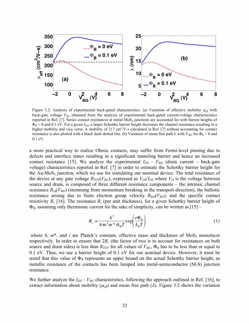
32
a more practical way to realize Ohmic contacts, may suffer from Fermi-level pinning due to defects and interface states resulting in a significant tunneling barrier and hence an increased contact resistance [15]. We analyze the experimental IDS – VBG (drain current – back-gate voltage) characteristics reported in Ref. [7] in order to estimate the Schottky barrier height for the Au-MoS2 junction, which we use for simulating our nominal device. The total resistance of the device at any gate voltage RTOT(VBG), expressed as VDS/IDS where VD is the voltage between source and drain, is composed of three different resistance components – the intrinsic channel resistance Rch(VBG) (stemming from momentum breaking in the transport direction), the ballistic resistance arising due to finite electron group velocity RBal(VBG), and the specific contact resistivity Rc [16]. The resistance Rc (per unit thickness), for a given Schottky barrier height of ΦB, assuming only thermionic current for the sake of simplicity, can be written as [15] –
Rc =h3
4πe2m * tkBTexp eΦB
kBT⎛
⎝ ⎜
⎞
⎠ ⎟ (1)
where h, m*, and t are Planck’s constant, effective mass and thickness of MoS2 monolayer respectively. In order to ensure that 2Rc (the factor of two is to account for resistances on both source and drain sides) is less than RTOT for all values of VBG, ΦB has to be less than or equal to 0.1 eV. Thus, we use a barrier height of 0.1 eV for our nominal device. However, it must be noted that this value of ΦB represents an upper bound on the actual Schottky barrier height, as metallic resistance of the contacts has been lumped into metal-semiconductor (M-S) junction resistance.
We further analyze the IDS – VBG characteristics, following the approach outlined in Ref. [16], to extract information about mobility (µeff) and mean free path (λ). Figure 3.2 shows the variation
Figure 3.2: Analysis of experimental back-gated characteristics. (a) Variation of effective mobility µeff with back-gate voltage VBG obtained from the analysis of experimental back-gated current-voltage characteristics reported in Ref. [7]. Series contact resistances at metal-MoS2 junctions are accounted for with barrier heights of ΦB = 0 and 0.1 eV. For a given IDS, a larger Schottky barrier height decreases the channel resistance resulting in a higher mobility and vice versa. A mobility of 217 cm2/V-s calculated in Ref. [7] without accounting for contact resistance is also plotted with a black dash-dotted line. (b) Variation of mean free path λ with VBG for ΦB = 0 and 0.1 eV.
2 0 2 4 6 8
100
150
200
250
300
350
VBG (V)
!ef
f (cm
2 /Vs)
B = 0 eV
B = 0.1 eV
(a)
2 0 2 4 6 85
10
15
20
25
VBG (V)
(nm
)
B = 0 eV
B = 0.1 eV
(b)

33
of µeff and λ with VBG for two different values of Schottky barrier heights of ΦB = 0 and 0.1 eV. The peak mobility extracted is about 220 cm2/V-s and 350 cm2/V-s for ΦB = 0 and 0.1 eV, respectively. The corresponding mean free paths are 15 and 22 nm.
3.2.2 SIMULATION APPROACH
The schematic of the simulated device are shown in Fig. 3.3. We perform simulations with an effective mass Hamiltonian to describe electronic transport through MoS2. Transport equations are solved iteratively together with Poisson’s equation until a self-consistency between charge density (calculated by analytical summation of transverse momentum modes within the first Brillouin zone) and electrostatic potential is achieved. Subsequently current is calculated as –
IDS =e2
my*kBT2π 3
dEkx∫ F−1/ 2µ1 − Ekx
kBT⎛
⎝ ⎜
⎞
⎠ ⎟ − F−1/ 2
µ2 − Ekx
kBT⎛
⎝ ⎜
⎞
⎠ ⎟
⎧ ⎨ ⎩
⎫ ⎬ ⎭ TSD (Ekx
) (2)
where F-1/2(.) denotes the Fermi-Dirac integral of order -1/2, TSD(.) is the transmission coefficient from source to drain, µ1 and µ2 are source and drain electrochemical potentials, ħ, my
*, e, kB, T, and are reduced Planck’s constant, transverse effective mass, elementary charge, Boltzmann constant, temperature, and longitudinal energy respectively. Gate leakage current is ignored. The conduction band effective mass along the transport direction (x) is calculated to be 0.45m0 (K → Γ), m0 being the free electron mass, from the dispersion relations of monolayer MoS2 [11]. A calculation of effective mass along K → M yields a similar value to the first order. Hence we assume the transverse effective mass to be identical to that along the transport direction, for the sake of simplicity. The Hamiltonian of the metallic regions at source and drain is modeled using an effective mass close to m0 (1.01m0) [17], and Dirichlet boundary conditions are imposed at the contacts. We use a dielectric constant of 3.3 for MoS2 [18], [19].
Detailed device parameters used in this work are provided in the caption of Fig. 3.3. For the simulated device, source and drain work functions are assumed to be the same as that of the gate. A grid spacing as small as 0.1 nm along x direction ensures the presence of states in both contact and channel regions in the entire energy range of interest within a single band description of
Figure 3.3: Schematic cross section of a monolayer MoS2 transistor. The channel is an MoS2 monolayer, and the source and drain contacts are metals such as gold (Au), which could make a good contact with a small Schottky barrier at the junction. The gate electrode is separated by HfO2 gate oxide (κ = 25). The nominal device has the following parameters: Gate length LG = 15 nm, HfO2 gate oxide thickness tox = 2.8 nm, gate underlap of 2 nm at each side, Schottky barrier height of ΦB = 0.1 eV, power supply voltage of 0.5 V.
Substrate
Source
Gate Oxide
Monolayer MoS2
Drain

34
effective mass Hamiltonian. We choose the gate length to be 15 nm so that the device operates away from the diffusive limit where the transport is predominantly limited by scattering, thereby making our performance projections realistic. An underlap of 2 nm each on the source and the drain sides is introduced to reduce the fringe capacitances without significantly increasing the series resistance.
3.3 RESULTS AND DISCUSSION
3.3.1 TRANSFER CHARACTERISTICS
The key device characteristics of MoS2 transistors are shown in Figs. 3.4-3.7. The transfer characteristics reveal that the maximum current (Imax) is ~1.6 mA/µm. However, we note that in
Figure 3.4: (a) IDS – VGS characteristics at VDS = 0.05 and 0.5 V on logarithmic (left axis) and linear scales (right axis). For the nominal device simulated, a maximum ON current as high as 1.6 mA/µm and a subthreshold swing (SS = ∂VGS/∂log10(IDS)) close to 60 mV/decade can be achieved. Drain-induced barrier lowering (DIBL) is as small as 10 mV/V even with very short channel length. (b) ION versus ION/IOFF for VD = 0.4, 0.5, and 0.6 V. With VD = 0.5 V, ION can be as high as 500 µA/µm with 4 orders of magnitude in ON-OFF current ratio. For the same ON current, ION/IOFF > 105 can be achieved with 0.6 V of drain voltage. (c) Transconductance (gm = ∂IDS/∂VGS) vs. VGS at VDS = 0.5 V. The gm is as large as 4.4 mS/µm for the nominal device within the voltage range considered in this study.
!!"# !!"$# ! !"$# !"# !"%#
&!!'
&!!(
&!!$
&!!
&!$
&!(
!!"# !!"$# ! !"$# !"# !"%#!
!"#
&
&"#
$
VGS (V)!I D
S (
mA
/!m
)!
I DS (!
A/!
m)!
VDS = 0.5 V!
0.05 V!
0.05 V!
0.5 V!
101 103 105 107 109
10 1
101
103
ION/IOFF
I ON
(µA
/µm
)
VDS = 0.4 VVDS = 0.5 VVDS = 0.6 V
(b)
0.5 0.3 0.1 0.1 0.3 0.5 0.70
1
2
3
4
5
VGS (V)
g m (m
S/µ
m)
(c)
(a)
35
case of reflection-less contacts, Imax can be even larger due to the non-parabolicity present in the conduction band of monolayer MoS2 wherein a satellite valley along K → Γ, which is only about 3kBT above the conduction band minima, contributes to enhanced density-of-states than what is predicted from our parabolic band approximation. The maximum-minimum current ratio (Imax/Imin) can be more than 10 orders of magnitude ignoring the gate leakage (Fig. 3.4 (a)). Gate-induced drain leakage (GIDL), one of the main leakage mechanisms that limits Imin in a conventional metal-oxide-semiconductor (MOS) geometry, is significantly less in case of an MoS2 transistor than in its Si counterpart due to the larger bandgap, and hence a smaller gate voltage can, in principle, further reduce Imin. It must be noted, however, that a more rigorous analysis to predict the maximum achievable Imax/Imin requires a multi-band Hamiltonian description (including valence band) to properly account for the effects of GIDL, which is beyond the scope of this study. In practical applications, what is more important than Imax/Imin is the ON-OFF current ratio (ION/IOFF), where voltage window between VON and VOFF is the same as power supply voltage (i.e. VON – VOFF = VDS). Therefore, ION/IOFF can be increased with a larger supply voltage for the same ON state current. For our nominal device structure (LG = 15 nm), drain-induced barrier lowering (DIBL) is negligibly small (10 mV/V, Fig. 3.4(a)) due to excellent electrostatics of the 2-D geometry, and hence a larger VDS can significantly increase ION/IOFF ratio for a given ION (Fig. 3.4(b)). We have also plotted the intrinsic device transconductance (gm = ∂IDS/∂VGS) from the IDS – VGS data at VDS = 0.5 V (Fig. 3.4(d)). The maximum gm is 4.4 mS/µm, which is still less in comparison to the peak gm that can be achieved, as gm is monotonically increasing over the entire range of VGS considered. This implies that at the largest gate voltage applied (VGS = 0.7 V), additional gate voltage could still significantly enhance current and the consequent voltage drop would mainly be across the semiconductor and not across the gate oxide. Therefore, for the simulated EOT, the operation of a monolayer MoS2 transistor is mainly dictated by its quantum capacitance and not by the oxide capacitance, the details of which will be discussed in a subsequent section.
3.3.2 OUTPUT CHARACTERISTICS
In Fig. 3.5, we can see that the output characteristics for a given VGS show saturation beyond VDS = 0.4 V with reasonably small output conductance (gd = 21, 51, and 133 µS/µm at VGS = 0.2, 0.3, and 0.4 V, respectively). We note that this is a direct consequence of the large bandgap of monolayer MoS2 because in the ballistic regime, it is the only factor that leads to saturation in output characteristics (scattering being the other factor in diffusive regime). It must be pointed out that this behavior is in stark contrast to graphene transistors wherein the absence of bandgap severely degrades their output resistance. Motivated by this, we explore, in Chapter 8, the potential suitability of MoS2 FETs for non-digital (analog and high-frequency RF) applications where drain current saturation is of primary importance.
3.3.3 EXTRAPOLATION TO DIFFUSIVE REGIME
The experimental characteristics in Ref. [7] show a maximum drive current of 2.5 µA/µm for a device with 500 nm gate length. Therefore, it is instructive to examine how the transfer characteristics for an optimized device with similar gate length would look like. Using the mean free path extracted from the experimental characteristics (Fig. 3.2 (b)), we calculate the corresponding IDS – VGS characteristics by multiplying the ballistic current from our simulations with λmax/(Lch+λmax) (where λmax and Lch are the peak mean free path and channel length,
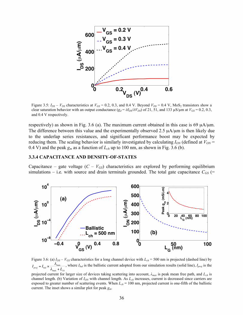
36
respectively) as shown in Fig. 3.6 (a). The maximum current obtained in this case is 69 µA/µm. The difference between this value and the experimentally observed 2.5 µA/µm is then likely due to the underlap series resistances, and significant performance boost may be expected by reducing them. The scaling behavior is similarly investigated by calculating ION (defined at VON = 0.4 V) and the peak gm as a function of Lch up to 100 nm, as shown in Fig. 3.6 (b).
3.3.4 CAPACITANCE AND DENSITY-OF-STATES
Capacitance – gate voltage (C – VGS) characteristics are explored by performing equilibrium simulations – i.e. with source and drain terminals grounded. The total gate capacitance CGS (=
Figure 3.5: IDS – VDS characteristics at VGS = 0.2, 0.3, and 0.4 V. Beyond VDS = 0.4 V, MoS2 transistors show a clear saturation behavior with an output conductance (gd = ∂IDS/∂VDS) of 21, 51, and 133 µS/µm at VGS = 0.2, 0.3, and 0.4 V respectively.
0 0.2 0.4 0.60
200
400
600
VDS (V)
I DS (µ
A/µ
m)
VGS = 0.2 VVGS = 0.3 VVGS = 0.4 V
Figure 3.6: (a) IDS – VGS characteristics for a long channel device with Lch = 500 nm is projected (dashed line) by
Iproj = Ibal ×λmax
λmax + Lch, where Ibal is the ballistic current adopted from our simulation results (solid line), Iproj is the
projected current for larger size of devices taking scattering into account, λmax is peak mean free path, and Lch is channel length. (b) Variation of ION with channel length. As Lch increases, current is decreased since carriers are exposed to greater number of scattering events. When Lch = 100 nm, projected current is one-fifth of the ballistic current. The inset shows a similar plot for peak gm.
0.4 0 0.4 0.810 8
10 4
100
104
VGS (V)
I DS (µ
A/µ
m)
BallisticLch = 500 nm
(a)
0 50 1000
100
200
300
400
500
600
LG
(nm)
I ON
(µ
A/µ
m)
0 20 40 60 80 1000
2
4
LG
(nm)
Peak g
m (
mS
/µm
)
(b)
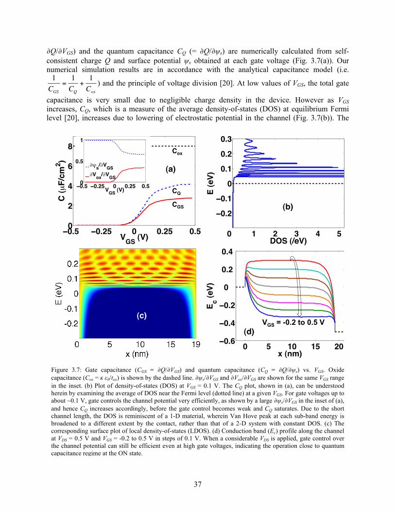
37
∂Q/∂VGS) and the quantum capacitance CQ (= ∂Q/∂ψs) are numerically calculated from self-consistent charge Q and surface potential ψs obtained at each gate voltage (Fig. 3.7(a)). Our numerical simulation results are in accordance with the analytical capacitance model (i.e.
1CGS
=1CQ
+1Cox
) and the principle of voltage division [20]. At low values of VGS, the total gate
capacitance is very small due to negligible charge density in the device. However as VGS increases, CQ, which is a measure of the average density-of-states (DOS) at equilibrium Fermi level [20], increases due to lowering of electrostatic potential in the channel (Fig. 3.7(b)). The
Figure 3.7: Gate capacitance (CGS = ∂Q/∂VGS) and quantum capacitance (CQ = ∂Q/∂ψs) vs. VGS. Oxide capacitance (Cox = ĸ ε0/tox) is shown by the dashed line. ∂ψs/∂VGS and ∂Vox/∂VGS are shown for the same VGS range in the inset. (b) Plot of density-of-states (DOS) at VGS = 0.1 V. The CQ plot, shown in (a), can be understood herein by examining the average of DOS near the Fermi level (dotted line) at a given VGS. For gate voltages up to about ~0.1 V, gate controls the channel potential very efficiently, as shown by a large ∂ψs/∂VGS in the inset of (a), and hence CQ increases accordingly, before the gate control becomes weak and CQ saturates. Due to the short channel length, the DOS is reminiscent of a 1-D material, wherein Van Hove peak at each sub-band energy is broadened to a different extent by the contact, rather than that of a 2-D system with constant DOS. (c) The corresponding surface plot of local density-of-states (LDOS). (d) Conduction band (Ec) profile along the channel at VDS = 0.5 V and VGS = -0.2 to 0.5 V in steps of 0.1 V. When a considerable VDS is applied, gate control over the channel potential can still be efficient even at high gate voltages, indicating the operation close to quantum capacitance regime at the ON state.
(c)
! " #! #" $!!!%&
!!%'
!!%$
!(((
!%$(
!%'(
)(*+,-
./(*01-
VGS
= -0.2 to 0.5 V
(d)
!!"# !!"$# ! !"$# !"#!
$
%
&
'
()*+,(-
.+,µ/012$-
.)*
.3
.45
!!"# !!"$# ! !"$# !"#!
!"#
%
&'()*&+
!",-!&
'(
!&./-!&
'(
Cox!
CQ!
CGS!
(a)
0 1 2 3 4 5
0.2
0.1
0
0.1
0.2
0.3
DOS (/eV)
E (e
V)(b)

38
saturation in CQ to a value smaller than the theoretically expected quantum capacitance (
CQ2−D = e
2m *π2 ) is a result of reduced DOS in the channel due to wavefunction reflections at
the contacts. At even larger gate voltages, the gate efficiency (∂ψs/∂VGS) decreases significantly (inset of Fig. 3.7(a)) due to charge accumulation and screening effect, leading to saturation in CQ. It must, however, be noted that under non-equilibrium conditions (with finite VDS), the gate control over channel electrostatics is good even at large gate voltages (∂(Ec/e)/∂VGS = 0.78 at VGS = 0.5 V as shown in Fig. 3.7(d)) due to lack of charge accumulation – an indication of the fact that the device operates closer to the quantum capacitance regime than the oxide capacitance regime.
3.3.5 GATE OXIDE AND CONTACTS
It has been reported that high-ĸ dielectric plays an important role in improving the monolayer MoS2 mobility and hence the device performance [7]. The gate oxide can also significantly affect the switching abruptness, and therefore we examine the effect of oxide thickness on subthreshold swing (SS). As shown in Fig. 3.8, SS increases linearly with oxide thickness, which is also predicted by the analytical subthreshold swing model in a conventional MOSFET [21]. At tox = 30 nm, our nominal device shows larger SS (79 mV/dec with LG = 15 nm) than the experimentally reported value for same oxide thickness (74 mV/dec with LG = 500 nm) [7], owing to short-channel behavior. However, with LG = 30 nm, SS improves considerably due to the suppression of short-channel effects (70.7 mV/dec for tox = 30 nm). Our extensive simulations predict that the reported value of SS = 74 mV/dec could be achieved with LG = 23 nm with tox = 30 nm. We also analyzed the electrostatics of the exact geometry reported in Ref. [7] at OFF state by solving the Laplace equation and confirmed the ∂(Ec/e)/∂VGS to be equal to 1, implying that SS is expected to be 60 mV/dec. Hence we believe that there exists considerable room for optimization of gate dielectrics in MoS2 transistors.
In fabricating monolayer MoS2 transistors, gold (Au) has been used to create an Ohmic contact – Schottky contact with negligible barrier height [7]. Our simulations show that the Schottky
Figure 3.8: Variation of subthreshold swing with oxide thickness. Subthreshold swing (SS) vs. oxide thickness (tox) with gate length of LG = 15 and 30 nm. SS increases linearly with oxide thickness due to the decrease in Cox. For the same tox, the swing of a device with longer gate length is significantly smaller due to immunity to short-channel effects. The diamond (in brown) shows the experimental data from Ref. [7], implying that the gate efficiency, in practice, could be significantly improved by optimization.
0 10 20 3060
70
80
90
tox (nm)
SS (m
V/de
c)
Lch = 15 nmLch = 30 nm
Experiment (Ref. [7])
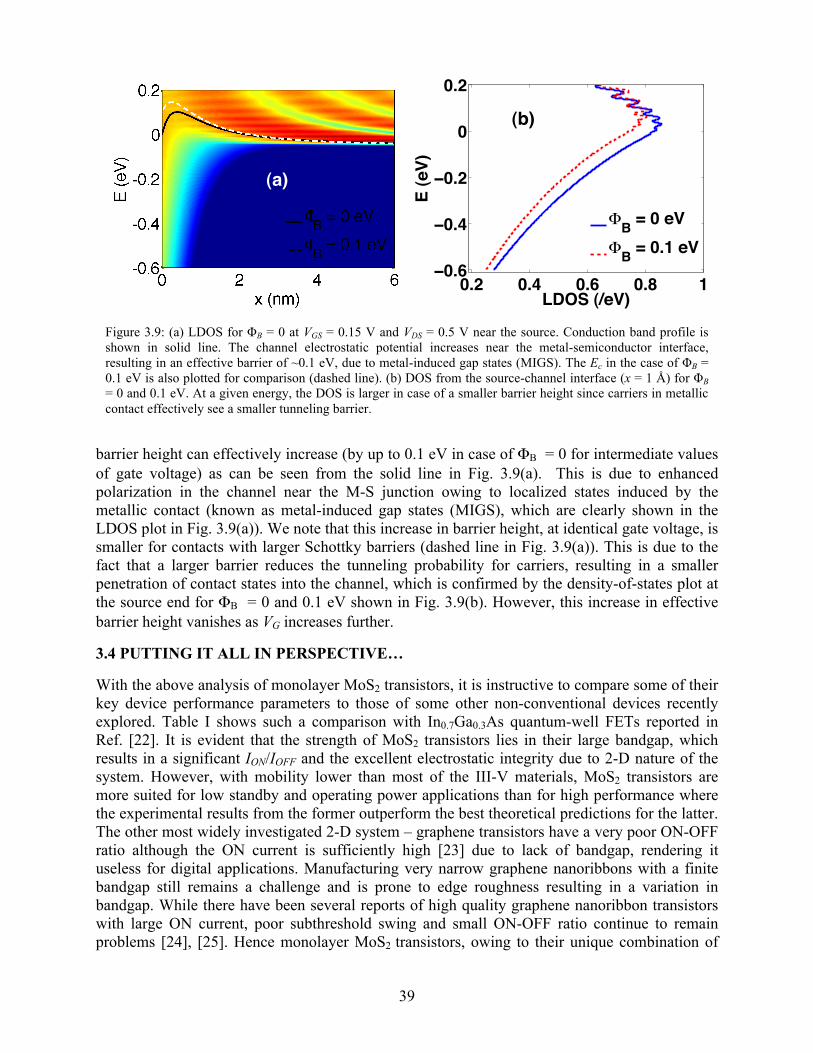
39
barrier height can effectively increase (by up to 0.1 eV in case of ΦB = 0 for intermediate values of gate voltage) as can be seen from the solid line in Fig. 3.9(a). This is due to enhanced polarization in the channel near the M-S junction owing to localized states induced by the metallic contact (known as metal-induced gap states (MIGS), which are clearly shown in the LDOS plot in Fig. 3.9(a)). We note that this increase in barrier height, at identical gate voltage, is smaller for contacts with larger Schottky barriers (dashed line in Fig. 3.9(a)). This is due to the fact that a larger barrier reduces the tunneling probability for carriers, resulting in a smaller penetration of contact states into the channel, which is confirmed by the density-of-states plot at the source end for ΦB = 0 and 0.1 eV shown in Fig. 3.9(b). However, this increase in effective barrier height vanishes as VG increases further.
3.4 PUTTING IT ALL IN PERSPECTIVE…
With the above analysis of monolayer MoS2 transistors, it is instructive to compare some of their key device performance parameters to those of some other non-conventional devices recently explored. Table I shows such a comparison with In0.7Ga0.3As quantum-well FETs reported in Ref. [22]. It is evident that the strength of MoS2 transistors lies in their large bandgap, which results in a significant ION/IOFF and the excellent electrostatic integrity due to 2-D nature of the system. However, with mobility lower than most of the III-V materials, MoS2 transistors are more suited for low standby and operating power applications than for high performance where the experimental results from the former outperform the best theoretical predictions for the latter. The other most widely investigated 2-D system – graphene transistors have a very poor ON-OFF ratio although the ON current is sufficiently high [23] due to lack of bandgap, rendering it useless for digital applications. Manufacturing very narrow graphene nanoribbons with a finite bandgap still remains a challenge and is prone to edge roughness resulting in a variation in bandgap. While there have been several reports of high quality graphene nanoribbon transistors with large ON current, poor subthreshold swing and small ON-OFF ratio continue to remain problems [24], [25]. Hence monolayer MoS2 transistors, owing to their unique combination of
Figure 3.9: (a) LDOS for ΦB = 0 at VGS = 0.15 V and VDS = 0.5 V near the source. Conduction band profile is shown in solid line. The channel electrostatic potential increases near the metal-semiconductor interface, resulting in an effective barrier of ~0.1 eV, due to metal-induced gap states (MIGS). The Ec in the case of ΦB = 0.1 eV is also plotted for comparison (dashed line). (b) DOS from the source-channel interface (x = 1 Å) for ΦB = 0 and 0.1 eV. At a given energy, the DOS is larger in case of a smaller barrier height since carriers in metallic contact effectively see a smaller tunneling barrier.
(a)
0.2 0.4 0.6 0.8 1
0.4
0.2
0
0.2
0.6LDOS (/eV)
E (e
V)
B = 0 eV
B = 0.1 eV
(b)
40
exquisite electrostatic integrity and large bandgap, can prove to be a better alternative for low power applications than several of the non-Si devices already explored.
To summarize, we have projected the ultimate scaling limit of monolayer MoS2 transistors by performing self-consistent quantum transport simulations. The key features of MoS2 transistors are (i) large gm (4.4 mS/µm) due to low DOS, (ii) significant Imax/Imin (> 1010) owing to a large bandgap, and (iii) excellent short channel behavior (DIBL < 10 mV/V and SS ~60 mV/dec) resulting from enhanced gate control. Along with these very good electrical characteristics, compatibility with present-day CMOS processing technology due to planarity of MoS2 monolayer makes MoS2 transistors one of the most viable candidates for future low power applications. Further, the properties of monolayer MoS2 like high thermal stability, chemical inertness, transparency, flexibility and relative inexpensiveness give MoS2 transistors a unique advantage for several low-cost electronic applications.
3.5 SUMMARY
We conclude the chapter by noting that by simulating the behavior of short-channel monolayer MoS2 MOSFETs, in addition to gaining insights about the specific material-system, we also obtain a great deal of confidence in the correctness of various results of BQTS – albeit only at a qualitative level so far – for they make intuitive sense and are in agreement with our understanding of semiconductor devices. From next chapter onwards, we start investigating the tunneling problem in detail, first by asking if a fully quantum-mechanical treatment is indeed essential, and subsequently by going onto to show that the answer to it is in the positive. We then provide some comparison of our results with experimental, two-terminal data before examining three-terminal devices in Chapter 5.
3.6 REFERENCES
[1] J. A. Wilson, and A. D. Yoffe, “The transition metal dichalcogenides discussion and interpretation of the observed optical, electrical and structural properties,” Adv. Phys., vol. 18, no. 73, pp. 193-335, 1969.
Lch
(nm)
EOT
(Å)
Imax
(mA/µm)
Peak gm
(mS/µm)
Max.
ION/IOFF
Min. SS
(mV/dec)
In0.7Ga0.3As QW-FET (Ref. [22]) 75 22 0.49 1.75 312 85
Monolayer MoS2 FET 75 22 0.19 0.3 1.4×10⁷ 60
Table I: Comparison of key device performance parameters of In0.7Ga0.3As Quantum-well FET (Ref. [22]) and monolayer MoS2 FET of identical EOT and channel length.
41
[2] E. Gourmelon, O. Lignier, H. Hadouda, G. Couturier, J. C. Bernede, J. Tedd, J. Pouzed, and Salardenne, “MS2 (M = W, Mo) photosensitive thin films for solar cells,” J. Sol. Energy Mater. Sol. Cells, vol. 46, no. 2, pp. 115-121, 1997.
[3] W. K. Ho, J. C. Yu, J. Lin, J. G. Yu, and P. S. Li, “Preparation and Photocatalytic Behavior of MoS2 and WS2 Nanocluster Sensitized TiO2,” Langmuir, vol. 20, no. 14, pp. 5865-5869, 2004.
[4] X. Zong, H. Yan, G. Wu, G. Ma, F. Wen, L. Wang, and C. Li, “Enhancement of Photocatalytic H2 Evolution on CdS by Loading MoS2 as Cocatalyst under Visible Light Irradiation,” J. Am. Chem. Soc., vol. 130, no. 23, pp. 7176-7177, 2008.
[5] K. F. Mak, C. Lee, J. Hone, J. Shan, and T. F. Heinz, “Atomically Thin MoS2: A New Direct-Gap Semiconductor,” Phys. Rev. Lett., vol. 105, no. 13, pp. 136805-136808, 2010.
[6] A. Splendiani, L. Sun, Y. Zhang, T. Li, J. Kim, C. –Y. Chim, G. Galli and F. Wang, “Emerging Photoluminescence in Monolayer MoS2,” Nano Lett., vol. 10, no. 4, pp. 1271-1275, 2010.
[7] B. Radisavljevic, A. Radenovi, J. Brivio, V. Giacometti, and A. Kis, “Single-layer MoS2 transistors,” Nature Nanotech., vol. 6, no. 3, pp. 147-150, 2011.
[8] K. S. Novoselov, D. Jiang, F. Schedin, T. J. Booth, V. V. Khotkevich, S. V. Morozov, and A. K. Geim, “Two-dimensional atomic crystals,” Proc. Natl. Acad. Sci. U.S.A., vol. 102, no. 30, pp. 10451-10453, 2005.
[9] Gmelin Handbook of Inorganic and Organometallic Chemistry, 8th ed.; Springer-Verlag: Berlin, Vol. B7, 1995.
[10] R. F. Frindt, “Single Crystals of MoS2 Several Molecular Layers Thick,” J. Appl. Phys., vol. 37, no. 4, pp. 1928-1929, 1966.
[11] S. Lebègue, and E. Eriksson, “Electronic structure of two-dimensional crystals from ab initio theory,” Phys. Rev. B, vol. 79, no. 11, pp. 115409-115412, 2009.
[12] K. I. Bolotin, K. J. Sikes, Z. Jiang, M. Klima, G. Fudenberg, J. Hone, P. Kim, and H. L. Stormer, “Ultrahigh electron mobility in suspended graphene,” Sol. State Comm., vol. 146, no. 9-10, pp. 351-355, 2008.
[13] F. Chen, J. Xia, D. K. Ferry, and N. Tao, “Dielectric Screening Enhanced Performance in Graphene FET,” Nano Lett., vol. 9, no. 7, pp. 2571-2574, 2009.
[14] D. Jena, and A. Konar, “Enhancement of Carrier Mobility in Semiconductor Nanostructures by Dielectric Engineering,” Phys. Rev. Lett., vol. 98, no.13, pp. 136805-136808, 2007.
[15] S. M. Sze, “Physics of Semiconductor Devices,” 3rd ed., Wiley-Interscience, 2006.
[16] M. S. Lundstrom, “Physics of Nanoscale MOSFETs”, https://nanohub.org/resources/5306.

42
[17] We use the value of dielectric constant corresponding to that of bulk MoS2, as detailed electrical characterization data of monolayer MoS2 has not yet been reported.
[18] Molybdenum Disulfide; Kee Hing Cheung Kee Co., Ltd: Hong Kong, http://www.khck.hk/adgoogle/Molybdenum-Disulfide.htm (accessed July 12, 2011).
[19] J. J. Szczyrbowski, “A new simple method of determining the effective mass of an electron or the thickness of thin metal films,” J. Phys. D: Appl. Phys., vol. 19, no. 7, pp. 1257-1263, 1986.
[20] S. Datta, “Quantum Transport: Atom to Transistor,” Cambridge University Press; 2nd Edition, 2005.
[21] Y. Taur, and T. H Ning, “Fundamentals of Modern VLSI Devices,” Cambridge University Press, 1998.
[22] M. Radosavljevic, B. Chu-Kung, S. Corcoran, G. Dewey, M. K. Hudait, J. M. Fastenau, J. Kavalieros, W. K. Liu, D. Lubyshev, M. Metz, K. Millard, N. Mukherjee, W. Rachmady, U. Shah, and R. Chau, “Advanced High-K Gate Dielectric for High-Performance Short-Channel In0.7Ga0.3As Quantum Well Field Effect Transistors on Silicon Substrate for Low Power Logic Applications,” IEDM Tech Digest, pp. 319-322, 2009.
[23] F. Schwierz, “Graphene transistors,” Nature Nanotech., vol. 5, no. 7, pp. 487-496, 2010.
[24] X. Wang, Y. Ouyang, X. Li, H. Wang, J. Guo, and H. Dai, “Room-Temperature All-Semiconducting Sub-10-nm Graphene Nanoribbon Field-Effect Transistors,” Phys. Rev. Lett., vol. 100, no. 20, pp. 206803-206806 2008.
[25] L. Liao, J. Bai, R. Cheng, Y. -C. Lin, S. Jiang, Y. Huang, and X. Duan, “Top-Gated Graphene Nanoribbon Transistors with Ultrathin High-k Dielectrics,” Nano Lett., vol. 10, no. 5, pp. 1917-1921, 2010.

43
CHAPTER 4
ZENER TUNNELING – CONGRUENCE BETWEEN SEMICLASSICAL AND QUANTUM BALLISTIC FORMALISMS
In Chapter 3, we investigated a top-of-the-barrier device i.e., MOSFET, to examine the qualitative correctness of various results obtained using the Berkeley Quantum Transport Simulator. Having ascertained the same, we venture out to understand the tunneling problem in greater detail. We start with the following questions – (a) given that there exist several semi-classical approaches to approximate band-to-band, Zener tunneling in semiconductors, is there really a need to solve the more computationally intensive, rigorous quantum-mechanical version of the problem? (b) If so, is there correspondence between the two approaches in some regimes of operation where the former suffices? (c) If not, is there a way to obtain quantitative match between the two by modifying the semi-classical approach slightly? After having answered them, we turn to some quantitative benchmarking of simulator results with experimental data. In particular, we focus on two-terminal tunneling characteristics as they provide the simplest of the platforms to test, where extraneous effects are minimal and hence the comparison is more appropriate.
4.1 SEMICLASSICAL OR QUANTUM?
The semi-classical, constant-field, closed-form expression due to Kane [1], [2] that relates tunneling probability with quantities like bandgap, effective mass, electric field etc., derived using stationary phase approximation – leading to a solution of the kind obtained by Wentzel-Kramers-Brillouin (WKB) method except for an additional prefactor of π2/9 – has been used extensively to explain experimental Zener tunneling characteristics and to model band-to-band tunneling in device simulators [3], [4]. Prominent among the works that have attempted to extend this study to the case of non-uniform fields are the ones by Hurkx [5], which suggests the usage of peak electric field in the Kane’s expression for calculating current, by Takayanagi and Iwabuchi [6], which follows a similar prescription as Ref. [1] for a quadratic potential profile – resulting from abrupt doping, and more recently by Vandenberghe et al. [7], wherein an envelope function approximation is used within a 2 band k.p model to numerically solve the Schrödinger equation.
As useful as these approaches are, they also suffer from certain limitations, some of which are present even in Kane’s original formulation – (a) semi-classical behavior, implying that the crystal momentum k is expressed as a function of position – a violation of uncertainty principle; (b) inadequate number of basis functions, as a result of which a realistic band-structure (both real and imaginary) is difficult to describe, leading to inaccurate calculation of tunneling rate; (c) non-self-consistent determination of the potential energy profile in the device for a given set of doping and bias conditions.
The consequences of the aforementioned factors are particularly severe in case of large electric fields [8] – a characteristic feature of modern day devices with ultra-small dimensions, wherein a full quantum-mechanical treatment of the tunneling problem – a computationally intensive exercise, is required. Previously, this problem has been addressed by Luisier and Klimeck in case
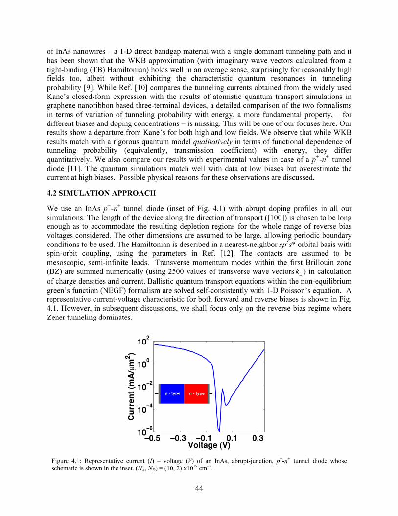
44
of InAs nanowires – a 1-D direct bandgap material with a single dominant tunneling path and it has been shown that the WKB approximation (with imaginary wave vectors calculated from a tight-binding (TB) Hamiltonian) holds well in an average sense, surprisingly for reasonably high fields too, albeit without exhibiting the characteristic quantum resonances in tunneling probability [9]. While Ref. [10] compares the tunneling currents obtained from the widely used Kane’s closed-form expression with the results of atomistic quantum transport simulations in graphene nanoribbon based three-terminal devices, a detailed comparison of the two formalisms in terms of variation of tunneling probability with energy, a more fundamental property, – for different biases and doping concentrations – is missing. This will be one of our focuses here. Our results show a departure from Kane’s for both high and low fields. We observe that while WKB results match with a rigorous quantum model qualitatively in terms of functional dependence of tunneling probability (equivalently, transmission coefficient) with energy, they differ quantitatively. We also compare our results with experimental values in case of a p+-n+ tunnel diode [11]. The quantum simulations match well with data at low biases but overestimate the current at high biases. Possible physical reasons for these observations are discussed.
4.2 SIMULATION APPROACH
We use an InAs p+-n+ tunnel diode (inset of Fig. 4.1) with abrupt doping profiles in all our simulations. The length of the device along the direction of transport ([100]) is chosen to be long enough as to accommodate the resulting depletion regions for the whole range of reverse bias voltages considered. The other dimensions are assumed to be large, allowing periodic boundary conditions to be used. The Hamiltonian is described in a nearest-neighbor sp3s* orbital basis with spin-orbit coupling, using the parameters in Ref. [12]. The contacts are assumed to be mesoscopic, semi-infinite leads. Transverse momentum modes within the first Brillouin zone (BZ) are summed numerically (using 2500 values of transverse wave vectors
k⊥ ) in calculation of charge densities and current. Ballistic quantum transport equations within the non-equilibrium green’s function (NEGF) formalism are solved self-consistently with 1-D Poisson’s equation. A representative current-voltage characteristic for both forward and reverse biases is shown in Fig. 4.1. However, in subsequent discussions, we shall focus only on the reverse bias regime where Zener tunneling dominates.
Figure 4.1: Representative current (I) – voltage (V) of an InAs, abrupt-junction, p+-n+ tunnel diode whose schematic is shown in the inset. (NA, ND) = (10, 2) x1018 cm-3.
0.5 0.3 0.1 0.1 0.310 6
10 4
10 2
100
102
Voltage (V)
Cur
rent
(mA
/µm
2 )
p - type n - type
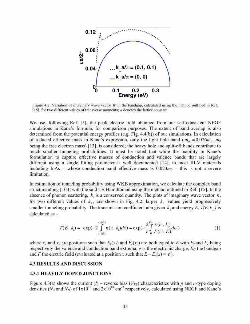
45
We use, following Ref. [5], the peak electric field obtained from our self-consistent NEGF simulations in Kane’s formula, for comparison purposes. The extent of band-overlap is also determined from the potential energy profiles (e.g. Fig. 4.4(b)) of our simulations. In calculation of reduced effective mass in Kane’s expression, only the light hole band (
mlh = 0.026m0, m0 being the free electron mass) [13], is considered; the heavy hole and split-off bands contribute to much smaller tunneling probabilities. It must be noted that while the inability in Kane’s formulation to capture effective masses of conduction and valence bands that are largely different using a single fitting parameter is well documented [14], in most III-V materials including InAs – whose conduction band effective mass is 0.023m0 – this is not a severe limitation.
In estimation of tunneling probability using WKB approximation, we calculate the complex band structure along [100] with the said TB Hamiltonian using the method outlined in Ref. [15]. In the absence of phonon scattering,
k⊥ is a conserved quantity. The plots of imaginary wave vector
κ , for two different values of
k⊥ , are shown in Fig. 4.2; larger
k⊥ values yield progressively smaller tunneling probability. The transmission coefficient at a given
k⊥ and energy E, T(E,
k⊥ ) is calculated as –
T(E, k⊥) = exp(−2 κ(x, k⊥)dx) = exp(− 2ex1 (E )
x2 (E )
∫ κ(ε ', k⊥)F(ε ', E)0
EG
∫ dε ') (1)
where x1 and x2 are positions such that Ev(x1) and Ec(x2) are both equal to E with Ev and Ec being respectively the valence and conduction band extrema, e is the electronic charge, EG the bandgap and F the electric field (evaluated at a position x such that E – Ev(x) =
ε').
4.3 RESULTS AND DISCUSSION
4.3.1 HEAVILY DOPED JUNCTIONS
Figure 4.3(a) shows the current (I) – reverse bias (VRB) characteristics with p and n-type doping densities (NA and ND) of 1x10¹⁹ and 2x1018 cm-3 respectively, calculated using NEGF and Kane’s
Figure 4.2: Variation of imaginary wave vector
κ in the bandgap, calculated using the method outlined in Ref. [15], for two different values of transverse momenta; a denotes the lattice constant.
0 0.1 0.2 0.30
0.04
0.08
0.12
Energy (eV)
!a
/2"
k#a/" = (0.1, 0.1)
k#a/" = (0, 0)
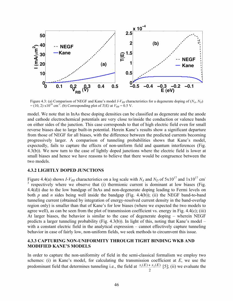
46
model. We note that in InAs these doping densities can be classified as degenerate and the anode and cathode electrochemical potentials are very close to/inside the conduction or valence bands on either sides of the junction. This case corresponds to that of high electric field even for small reverse biases due to large built-in potential. Herein Kane’s results show a significant departure from those of NEGF for all biases, with the difference between the predicted currents becoming progressively larger. A comparison of tunneling probabilities shows that Kane’s model, expectedly, fails to capture the effects of non-uniform field and quantum interferences (Fig. 4.3(b)). We now turn to the case of lightly doped junctions where the electric field is lower at small biases and hence we have reasons to believe that there would be congruence between the two models.
4.3.2 LIGHTLY DOPED JUNCTIONS
Figure 4.4(a) shows I-VRB characteristics on a log scale with NA and ND of 5x10¹⁷ and 1x1017 cm-
3 respectively where we observe that (i) thermionic current is dominant at low biases (Fig. 4.4(d)) due to the low bandgap of InAs and non-degenerate doping leading to Fermi levels on both p and n sides being well inside the bandgap (Fig. 4.4(b)); (ii) the NEGF band-to-band tunneling current (obtained by integration of energy-resolved current density in the band-overlap region only) is smaller than that of Kane’s for low biases (where we expected the two models to agree well), as can be seen from the plot of transmission coefficient vs. energy in Fig. 4.4(c); (iii) At larger biases, the behavior is similar to the case of degenerate doping – wherein NEGF predicts a larger tunneling probability (Fig. 4.3(b)). In light of this, noting that Kane’s model – with a constant electric field in the analytical expression – cannot effectively capture tunneling behavior in case of fairly low, non-uniform fields, we seek methods to circumvent this issue.
4.3.3 CAPTURING NON-UNIFORMITY THROUGH TIGHT BINDING WKB AND MODIFIED KANE’S MODELS
In order to capture the non-uniformity of field in the semi-classical formalism we employ two schemes: (i) in Kane’s model, for calculating the transmission coefficient at E, we use the predominant field that determines tunneling i.e., the field at
x1(E) + x2(E)2
[5]; (ii) we evaluate the
Figure 4.3: (a) Comparison of NEGF and Kane’s model I-VRB characteristics for a degenerate doping of (NA, ND) = (10, 2) x1018 cm-3. (b) Corresponding plot of T(E) at VRB = 0.5 V.
0 0.1 0.2 0.3 0.4 0.50
10
20
30
40
50
VRB
(V)
I (m
A/µ
m2)
NEGF
Kane
(a)
!!"# !!"$ !!"% !!"& !!"'!
!"#
'
'"#
&
&"#()'!
!$
*)+,-.
/+*.
)0*12
)345,
(b)
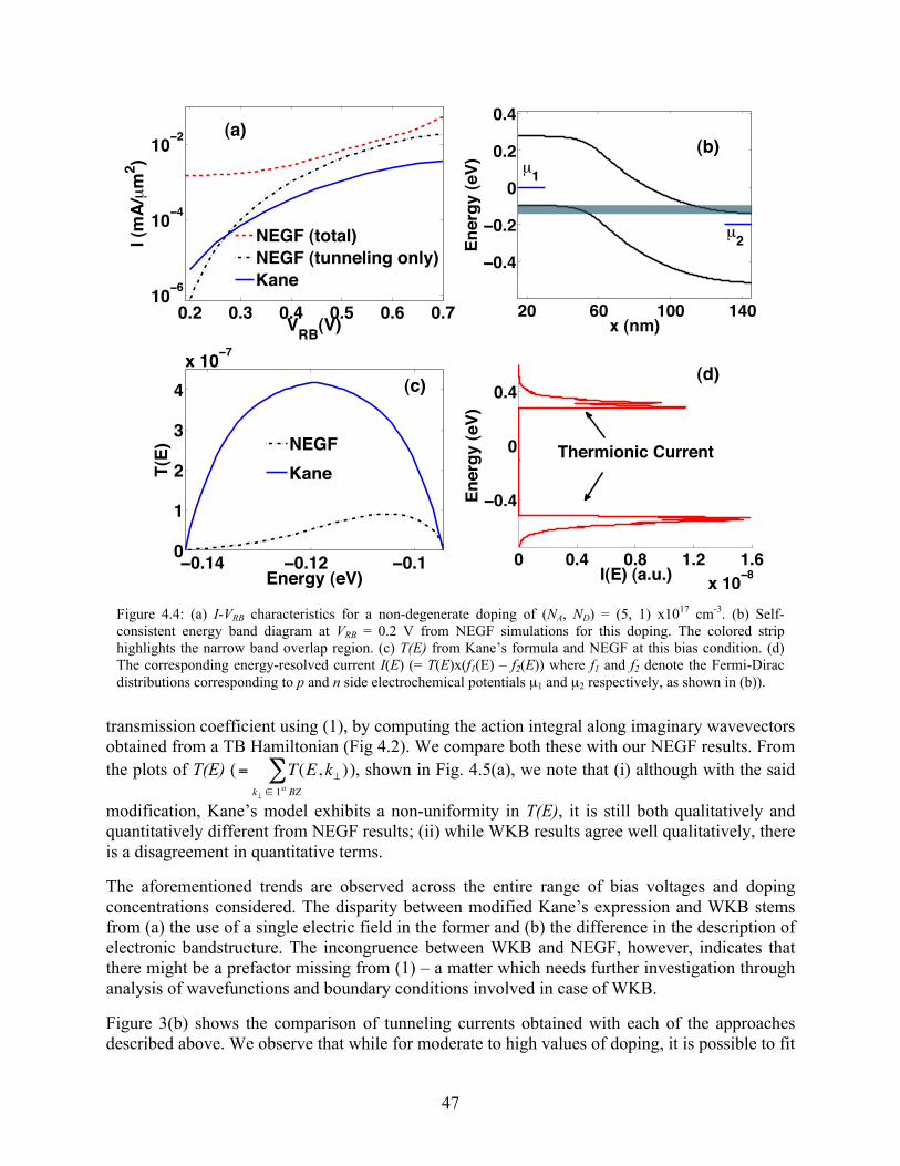
47
transmission coefficient using (1), by computing the action integral along imaginary wavevectors obtained from a TB Hamiltonian (Fig 4.2). We compare both these with our NEGF results. From the plots of T(E) (
= T(E,k⊥ ∈ 1st BZ
∑ k⊥ )), shown in Fig. 4.5(a), we note that (i) although with the said
modification, Kane’s model exhibits a non-uniformity in T(E), it is still both qualitatively and quantitatively different from NEGF results; (ii) while WKB results agree well qualitatively, there is a disagreement in quantitative terms.
The aforementioned trends are observed across the entire range of bias voltages and doping concentrations considered. The disparity between modified Kane’s expression and WKB stems from (a) the use of a single electric field in the former and (b) the difference in the description of electronic bandstructure. The incongruence between WKB and NEGF, however, indicates that there might be a prefactor missing from (1) – a matter which needs further investigation through analysis of wavefunctions and boundary conditions involved in case of WKB.
Figure 3(b) shows the comparison of tunneling currents obtained with each of the approaches described above. We observe that while for moderate to high values of doping, it is possible to fit
Figure 4.4: (a) I-VRB characteristics for a non-degenerate doping of (NA, ND) = (5, 1) x1017 cm-3. (b) Self-consistent energy band diagram at VRB = 0.2 V from NEGF simulations for this doping. The colored strip highlights the narrow band overlap region. (c) T(E) from Kane’s formula and NEGF at this bias condition. (d) The corresponding energy-resolved current I(E) (= T(E)x(f1(E) – f2(E)) where f1 and f2 denote the Fermi-Dirac distributions corresponding to p and n side electrochemical potentials µ1 and µ2 respectively, as shown in (b)).
!"# !"$ !"% !"& !"' !"()!
!'
)!!%
)!!#
*+,
-*.
/0-1
23µ
1#.
45670-898:;.
45670-8<==>;?=@09=;A.
B:=>
(a)
20 60 100 140
0.4
0
0.4
0.2
0.2
x (nm)
Ener
gy (e
V)
µ2
µ1
(b)
0 0.4 0.8 1.2 1.6x 10 8
0.4
0
0.4
I(E) (a.u.)
Ener
gy (e
V)Thermionic Current
(d)
0.14 0.12 0.10
1
2
3
4x 10 7
Energy (eV)
T(E)
NEGFKane
(c)

48
reasonably well the results from both WKB and modified Kane’s models with those from NEGF within the bias range considered using a field-dependent prefactor (Fig. 3(c)), the mismatch in (i) current in case of light doping and (ii) conductance for large reverse biases, suggests the need for a more holistic approach in determination of this prefactor.
4.3.4 COMPARISON WITH TUNNEL DIODE DATA
We finally compare our results with experimental, two-terminal tunnel-diode data reported in Ref. [3] in the reverse bias region. The I-VRB characteristics for different doping densities along with experimental data are plotted in Fig. 4.6. A series resistance of 90 Ω, close to the value used in Ref. [3], is used. It can be clearly seen that while NEGF results agree well for small biases, it predicts larger current values for increasing VRB. It is conceivable that at higher biases phonon scattering may restrict the current and is the major source of discrepancy between simulation and experimental data.
Figure 4.5: (a) Plot of T(E) calculated from NEGF, WKB and modified Kane’s model expressions at VRB = 0.6 V for (NA, ND) = (6, 2) x1018 cm-3. (b) Corresponding I-VRB characteristics (c) Best global fitting of semi-classical characteristics in (b) to those from NEGF. The prefactors used in case of WKB and Kane’s model are respectively 3.8 and 13.5. (d) Similar characteristics for a lightly doped case – (NA, ND) = (2, 0.5) x1018 cm-3, showing discrepancy in fitting for small reverse biases. The respective prefactors are 5.1 and 20, which give a good match on a linear scale.
!!"## !!"$ !!"%# !!"&!
&
%
&"#
!"#
'(&!!$
)*+,-.(/+01
2/)1
(a)
! !"# !"$ !"%&!
!#
&!!&
&!!
&!&
&!#
'()*+',
-*+./0µ.#,
1234
56)
789:;:<9*6=><
(b)
0.2 0.4 0.60
20
40
60
80
VRB
(V)
I (m
A/µ
m2)
(c)
0.15 0.350.25
100
10 2
10 4
VRB (V)
I (m
A/µ
m2 )
(d)
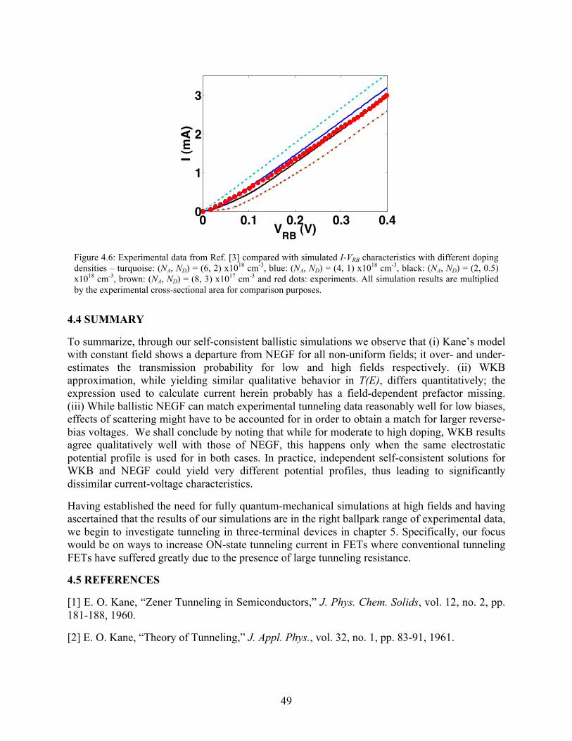
49
4.4 SUMMARY
To summarize, through our self-consistent ballistic simulations we observe that (i) Kane’s model with constant field shows a departure from NEGF for all non-uniform fields; it over- and under-estimates the transmission probability for low and high fields respectively. (ii) WKB approximation, while yielding similar qualitative behavior in T(E), differs quantitatively; the expression used to calculate current herein probably has a field-dependent prefactor missing. (iii) While ballistic NEGF can match experimental tunneling data reasonably well for low biases, effects of scattering might have to be accounted for in order to obtain a match for larger reverse-bias voltages. We shall conclude by noting that while for moderate to high doping, WKB results agree qualitatively well with those of NEGF, this happens only when the same electrostatic potential profile is used for in both cases. In practice, independent self-consistent solutions for WKB and NEGF could yield very different potential profiles, thus leading to significantly dissimilar current-voltage characteristics.
Having established the need for fully quantum-mechanical simulations at high fields and having ascertained that the results of our simulations are in the right ballpark range of experimental data, we begin to investigate tunneling in three-terminal devices in chapter 5. Specifically, our focus would be on ways to increase ON-state tunneling current in FETs where conventional tunneling FETs have suffered greatly due to the presence of large tunneling resistance.
4.5 REFERENCES
[1] E. O. Kane, “Zener Tunneling in Semiconductors,” J. Phys. Chem. Solids, vol. 12, no. 2, pp. 181-188, 1960.
[2] E. O. Kane, “Theory of Tunneling,” J. Appl. Phys., vol. 32, no. 1, pp. 83-91, 1961.
Figure 4.6: Experimental data from Ref. [3] compared with simulated I-VRB characteristics with different doping densities – turquoise: (NA, ND) = (6, 2) x1018 cm-3, blue: (NA, ND) = (4, 1) x1018 cm-3, black: (NA, ND) = (2, 0.5) x1018 cm-3, brown: (NA, ND) = (8, 3) x1017 cm-3 and red dots: experiments. All simulation results are multiplied by the experimental cross-sectional area for comparison purposes.
0 0.1 0.2 0.3 0.40
1
2
3
VRB
(V)
I (m
A)
50
[3] J. C. Ho, A. C. Ford, Y. L. Cheuh, O. Ergen, K. Takei, G. Smith, P. Majhi, J. Bennett, and A. Javey, “Nanoscale doping of InAs via sulfur monolayers,” Appl. Phys. Lett., vol. 95, no.7, pp. 072108-072110, 2009.
[4] Sentaurus Device User Guide, Version Z-2007.03, Mountain View, California: Synopsys, Inc., 2007.
[5] G. A. M. Hurkx, “On the modelling of tunnelling currents in reverse-biased p-n junctions,” Solid State Electron., vol. 32, no.8, pp. 665-668, 1989.
[6] M. Takayanagi and S. Iwabuchi, “Theory of band-to-band tunneling under nonuniform electric fields for subbreakdown leakage currents,” IEEE Trans. Electron Devices, vol. 38, no. 6, pp. 1425-1431, 1991.
[7] W. Vandenberghe, B. Sorée, W. Magnus and G. Groeseneken, “Zener tunneling in semiconductors under nonuniform electric fields,” J. Appl. Phys., vol. 107, no. 5, pp. 054520-054526, 2010.
[8] While not treating phonons explicitly, Kane states that his analysis is valid only when
τ , the mean scattering time for carriers, is much less than the Bloch oscillation period
τBloch (=
KeF , where
is the reduced Planck’s constant and K a reciprocal lattice vector) [1]. Assuming
τ ~ 0.52 ps (corresponding to a low-field electron mobility of 40,000 cm2/Vs [13]), this holds for F < 130 kV/cm (with K = 2π/a).
[9] M. Luisier and G. Klimeck, “Simulation of nanowire tunneling transistors: From the Wentzel–Kramers–Brillouin approximation to full-band phonon-assisted tunneling,” J. Appl. Phys., vol. 107, no. 8, pp. 084507-084512, 2010.
[10] Y. Gao, T. Low, and M. Lundstrom, “Possibilities for VDD = 0.1V Logic Using Carbon-Based Tunneling Field Effect Transistors,” VLSI Tech. Symp., pp. 180-181, 2009.
[11] Our choice of diode as opposed to tunneling field-effect transistor for the purposes of this study, unlike Refs. [9] and [10], is guided by two important factors – (i) the want to compare NEGF results with experimental data – plenty in case of former but significantly few in case of latter – and (ii) the necessity to eliminate effects of 2-D electrostatics whereby only the effects of applied reverse bias and doping on tunneling can be investigated.
[12] G. Klimeck, F. Oyafuso, T. B. Boykin, R. C. Bowen and P. von Allmen, “Development of a Nanoelectronic 3-D (NEMO 3-D) Simulator for Multimillion Atom Simulations and Its Application to Alloyed Quantum Dots,” CMES - Comp. Model Eng., vol. 3, no. 5, pp. 601-642, 2002.
[13] Ioffe Physico-Technical Institute, “InAs – Indium Arsenide,” Retrieved from http://www.ioffe.ru/SVA/NSM/Semicond/InAs/index.html
[14] E. Hatta, J. Nagao and K. Musaka, “Tunneling through a narrow‐gap semiconductor with different conduction‐ and valence‐band effective masses,” J. Appl. Phys., vol. 79, no. 3, pp. 1511-1514, 1996.

51
[15] Y. -C. Chang and J. N. Schulman, “Complex band structures of crystalline solids: An eigenvalue method,” Phys. Rev. B, vol. 25, no. 6, pp. 3975-3986, 1982.
52
CHAPTER 5
INDIUM ARSENIDE LATERAL AND VERTICAL BAND-TO-BAND TUNNELING TRANSISTORS In this chapter, we begin our investigation of three-terminal tunneling devices using BQTS. The conventional, gated p-i-n tunneling field-effect transistors (TFETs) have suffered from the issue of tunneling resistance even when the device is ON. Motivated by this, we choose InAs – a direct, narrow bandgap III-V semiconductor – to be our channel material in this study because of its potential in delivering large ON current. In this context, we examine a variant of the gated p-i-n structure, where there exists a heavily doped pocket in the source-channel overlap region. By comparing this with conventional TFETs at short channel-lengths, we determine the trade-offs governing steep turn-on and high ON-state current. Understanding the underlying physics in these geometries is instrumental in identifying directions for device optimization.
5.1 MOTIVATION
The recent interest in band-to-band tunneling transistors is due to their promise of overcoming the fundamental limit of subthreshold swing (60 mV/decade at room temperature) in case of classical MOS devices, thereby providing a path to significantly reduce supply voltage and power dissipation. The advantage of TFETs over MOSFETs in this regard has been discussed and demonstrated in various material systems [1]-[3]. However, the ON state current in TFETs is significantly lower than in MOSFETs owing to tunneling resistance, which arises due to carrier-tunneling between energy eigenstates of different symmetry (i.e. conduction and valence band). Hence it is critical to the design of TFETs to understand the factors governing ON current and subthreshold swing (SS). Hence we investigate the performance of InAs TFETs where tunneling occurs in the direction normal to the semiconductor-dielectric interface (vertical TFET from hereon) to see if there are any inherent advantages owing to either the device geometry or the nature of tunneling in these devices over conventional TFETs where the tunneling occurs from source to drain (lateral TFET from hereon). To this end, we perform self-consistent ballistic quantum mechanical simulations with multi-band Hamiltonian within the NEGF formalism in realistic-size devices. Our simulations show that vertical TFETs, due to an additional vertical tunneling component provide more ON current than their lateral counterparts. We also explore the design possibilities of vertical TFETs whereby we show that they can be optimized to yield steeper turn-on characteristics and smaller OFF currents than lateral TFETs. Our results also provide insight towards scaling (in terms of both body thickness and channel length) behavior of ultra-thin body vertical TFETs based on low bandgap and low effective-mass materials.
5.2 GEOMETRY AND SIMULATION DETAILS
Figure 5.1 shows the schematic of the cross section of simulated devices where the lateral TFET (Fig. 5.1(a)) is an ultra thin body double-gate InAs p-i-n TFET while the vertical InAs TFET (Fig. 5.1(b)) is a device with identical footprint except for a heavily doped n+ pocket in the gate-source overlap region. Our vertical TFET has an additional back-gate underneath the channel in comparison to the device structure proposed by Pratik et al. (see Fig. 2 of Ref. [5]) in order to have a better electrostatic control while keeping the vertical tunneling intact. The doping

53
densities, device dimensions and other parameters used in simulation are mentioned in the caption of Fig. 5.1. A 4 band Kane’s second order k.p Hamiltonian is used to describe the bandstructure of InAs [6]. The spurious states in the dispersion curves arising due to confinement are removed following standard techniques [7]. Spin-orbit coupling has been ignored in our simulations to reduce the computation time [8].
The Green’s function G, at a given total energy E, calculated using the self-consistent Born approximation is given by G(E) = [EI – H – Σ1 – Σ2]-1 where H is the Hamiltonian of the system, I an identity matrix and Σ1,2 the contact self-energies [9]. The self-energies are calculated by assuming semi-infinite leads using a technique due to Sancho et al. [10], while G is calculated using the recursive Green’s function algorithm [11]. We assume that the dimension of the devices is large along the width and hence use a periodic boundary condition in that direction. We note that while using a multi-band Hamiltonian, it is not possible to analytically sum over the momentum states along the width in calculation of electron and hole densities as can be done in
Figure 5.1: Schematic of the simulated devices: (a) lateral InAs TFET, and (b) vertical InAs TFET with a heavily doped n+ pocket (halo) in the gate-source overlap region. The doping profiles in all our simulations are abrupt with a source and drain doping of 5 1019 cm-3 and 5 1018 cm-3 respectively. The asymmetry in doping concentrations is motivated by the lower conduction band density of states in InAs and the need to suppress ambipolar conduction. In case of vertical TFET, we use a pocket doping of 5 1019 cm-3. Although the channel region is intrinsic, we use an n-type doping of 1 1015 cm-3 to account for unintentional doping arising due to defects. A 1.2 nm gate dielectric with = 15. 4 is used. The length of source and drain in our simulations is 20 nm each with a 10 nm overlap on the source side in case of vertical TFET. For 10 nm thick body, the pocket is 3.6 nm deep while for a body thickness of 6 nm, we use a pocket depth of 2.4 nm. The crystallographic direction is assumed to be (100) for transport and the body is confined along (001) direction. Also, difference in workfunction between semiconductor and gate metal,
Φms , is assumed to be zero.
!!"#$%&'(" "")&*+,"#"-$./"
0*1(!!
0*1(!!
23+.("
23+.("
(a)
!!"#$%&'("
"!""
)$'*(+"
"",&-./"#"0$12"
3-+(!!
3-+(!!
45.1("
45.1("
(b)
"
"
"
"
"
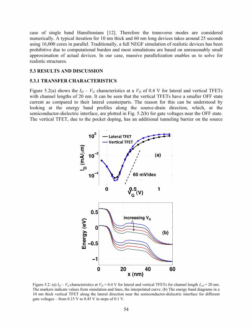
54
case of single band Hamiltonians [12]. Therefore the transverse modes are considered numerically. A typical iteration for 10 nm thick and 60 nm long devices takes around 25 seconds using 16,000 cores in parallel. Traditionally, a full NEGF simulation of realistic devices has been prohibitive due to computational burden and most simulations are based on unreasonably small approximation of actual devices. In our case, massive parallelization enables us to solve for realistic structures.
5.3 RESULTS AND DISCUSSION
5.3.1 TRANSFER CHARACTERISTICS
Figure 5.2(a) shows the ID – VG characteristics at a VD of 0.4 V for lateral and vertical TFETs with channel lengths of 20 nm. It can be seen that the vertical TFETs have a smaller OFF state current as compared to their lateral counterparts. The reason for this can be understood by looking at the energy band profiles along the source-drain direction, which, at the semiconductor-dielectric interface, are plotted in Fig. 5.2(b) for gate voltages near the OFF state. The vertical TFET, due to the pocket doping, has an additional tunneling barrier on the source
Figure 5.2: (a) ID – VG characteristics at VD = 0.4 V for lateral and vertical TFETs for channel length Lch = 20 nm. The markers indicate values from simulation and lines, the interpolated curve. (b) The energy band diagrams in a 10 nm thick vertical TFET along the lateral direction near the semiconductor-dielectric interface for different gate voltages – from 0.15 V to 0.45 V in steps of 0.1 V.
!"#$%"&'()*('
+$%,-"&'()*('
./'0+12$-'
60 mV/dec
(a)
! "! #! $!
!%
!!&'
!
!&'
()*+,-
.+/012)*/3- increasing VG!
(b)
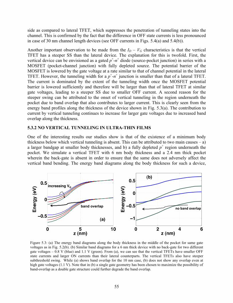
55
side as compared to lateral TFET, which suppresses the penetration of tunneling states into the channel. This is confirmed by the fact that the difference in OFF state currents is less pronounced in case of 30 nm channel length devices (see OFF currents in Figs. 5.4(a) and 5.4(b)).
Another important observation to be made from the ID – VG characteristics is that the vertical TFET has a steeper SS than the lateral device. The explanation for this is twofold. First, the vertical device can be envisioned as a gated p+-n+ diode (source-pocket junction) in series with a MOSFET (pocket-channel junction) with fully depleted source. The potential barrier of the MOSFET is lowered by the gate voltage at a rate similar to that of channel potential in the lateral TFET. However, the tunneling width for a p+-n+ junction is smaller than that of a lateral TFET. The current is dominated by the extent of the tunneling width once the MOSFET potential barrier is lowered sufficiently and therefore will be larger than that of lateral TFET at similar gate voltages, leading to a steeper SS due to smaller OFF current. A second reason for the steeper swing can be attributed to the onset of vertical tunneling in the region underneath the pocket due to band overlap that also contributes to larger current. This is clearly seen from the energy band profiles along the thickness of the device shown in Fig. 5.3(a). The contribution to current by vertical tunneling continues to increase for larger gate voltages due to increased band overlap along the thickness.
5.3.2 NO VERTICAL TUNNELING IN ULTRA-THIN FILMS
One of the interesting results our studies show is that of the existence of a minimum body thickness below which vertical tunneling is absent. This can be attributed to two main causes – a) a larger bandgap at smaller body thicknesses, and b) a fully depleted p+ region underneath the pocket. We simulate a vertical TFET with 6 nm body thickness and a 2.4 nm thick pocket wherein the back-gate is absent in order to ensure that the same does not adversely affect the vertical band bending. The energy band diagrams along the body thickness for such a device,
Figure 5.3: (a) The energy band diagrams along the body thickness in the middle of the pocket for same gate voltages as in Fig. 5.2(b). (b) Similar band diagrams for a 6 nm thick device with no back-gate for two different gate voltages – 0.8 V (blue) and 1.1 V (green). From (a), we can see that the vertical TFETs have smaller OFF state currents and larger ON currents than their lateral counterparts. The vertical TFETs also have steeper subthreshold swing. While (a) shows band overlap for the 10 nm case, (b) does not show any overlap even at high gate voltages (1.1 V). Note that in (b) a single gate geometry has been chosen to maximize the possibility of band-overlap as a double gate structure could further degrade the band overlap.
increasing VG!
band overlap
(a)
! " # $
!%
!!&'
!
!&'
()*+,-)
.+/012)*/3-
!"#$%!&#"'()*%+#
(b)
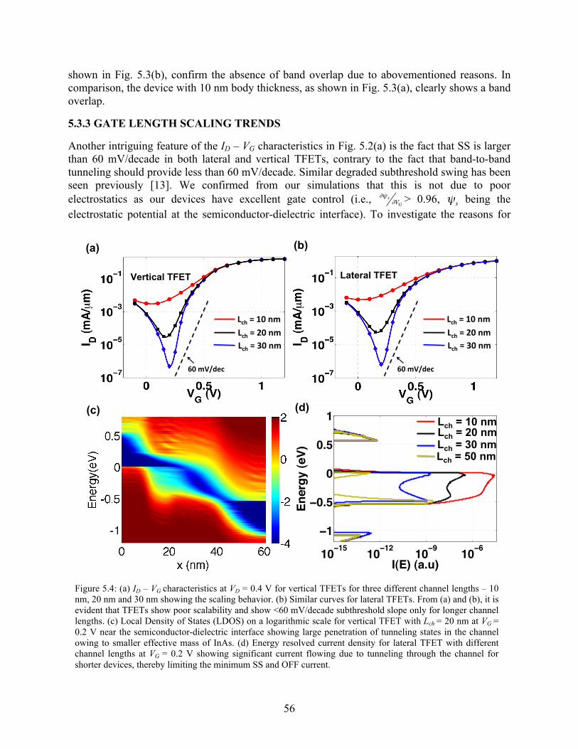
56
shown in Fig. 5.3(b), confirm the absence of band overlap due to abovementioned reasons. In comparison, the device with 10 nm body thickness, as shown in Fig. 5.3(a), clearly shows a band overlap.
5.3.3 GATE LENGTH SCALING TRENDS
Another intriguing feature of the ID – VG characteristics in Fig. 5.2(a) is the fact that SS is larger than 60 mV/decade in both lateral and vertical TFETs, contrary to the fact that band-to-band tunneling should provide less than 60 mV/decade. Similar degraded subthreshold swing has been seen previously [13]. We confirmed from our simulations that this is not due to poor electrostatics as our devices have excellent gate control (i.e.,
∂ψ s∂VG > 0.96,
ψs being the electrostatic potential at the semiconductor-dielectric interface). To investigate the reasons for
Figure 5.4: (a) ID – VG characteristics at VD = 0.4 V for vertical TFETs for three different channel lengths – 10 nm, 20 nm and 30 nm showing the scaling behavior. (b) Similar curves for lateral TFETs. From (a) and (b), it is evident that TFETs show poor scalability and show <60 mV/decade subthreshold slope only for longer channel lengths. (c) Local Density of States (LDOS) on a logarithmic scale for vertical TFET with Lch = 20 nm at VG = 0.2 V near the semiconductor-dielectric interface showing large penetration of tunneling states in the channel owing to smaller effective mass of InAs. (d) Energy resolved current density for lateral TFET with different channel lengths at VG = 0.2 V showing significant current flowing due to tunneling through the channel for shorter devices, thereby limiting the minimum SS and OFF current.
!"#$%&'()#
*)+#,#-"#.$#
*)+#,#/"#.$#
*)+#,#0"#.$#
Vertical TFET
!"#$%&'()#
*)+#,#-"#.$#
*)+#,#/"#.$#
*)+#,#0"#.$#
Lateral TFET
!"!!#
!"!!$
!"!%
!"!&
!!
!"'#
"
"'#
!
()*+,)-'.+
*/0123,)04+
Lch
= 10 nm
Lch
= 20 nm
Lch
= 30 nm
Lch
= 50 nm
(a) (b)
(c) (d)

57
this, we study the scaling behavior of vertical TFETs by varying the length of the channel. Figures 5.4(a) and (b) show the ID – VG characteristics of vertical and lateral TFETs respectively for three different lengths of the channel – 10 nm, 20 nm and 30 nm with all other parameters remaining the same.
Evident from the characteristics is the fact that these devices exhibit very poor scalability. The simulations show that this is mainly due to the fact that the conduction band effective mass in InAs is quite low (0.03m0 for a 10 nm thick body) which leads to huge penetration of wavefunctions into the channel and hence a large leakage current which limits the swing in TFETs. The local density-of-states (LDOS) plot on a logarithmic scale in Fig. 5.4(c) shows large penetration of tunneling states into the channel in the OFF state. Energy resolved current, I(E), given by T(E) (f1(E) – f2(E)), is plotted in Fig. 5.4(d). Here T(E) is the transmission probability at energy E and f1 and f2 are the Fermi-Dirac distributions corresponding to source and drain respectively. All the plots correspond to OFF state. From Fig. 5.4(d), the peak of the current appears in the energy range of 0 to -0.5 eV, where the band-gap in the channel should have stopped the current flow (see Fig. 5.4(c)). This then clearly points to direct source-to-drain tunneling that becomes increasingly severe as one goes down to smaller channel lengths.
5.4 SUMMARY
To summarize, using self-consistent NEGF simulations, we have shown that the vertical TFETs offer significant advantages over their lateral counterparts in terms of increased ON current and steeper SS. This is due to (i) an additional tunneling barrier in the current path at the OFF state that provides lower OFF current, (ii) a thinner tunneling barrier at the ON current that provides larger ON current, and (iii) finally, a vertical tunneling component in addition to a lateral one at the ON condition that further increases the drive current. However, we note that the aforementioned benefits are incremental in homojunction devices. This is because of poor scalability of both lateral and vertical TFETs in small EG and low effective-mass materials. In this study, we have restricted ourselves to using nominal device structures so as to retain our emphasis on the underlying physics. Nonetheless, the aforementioned points indicate that there exist several opportunities for device optimization by band-engineering either through strain or through heterostructures, and thereby for amplifying the advantages of vertical TFETs over conventional, lateral TFETs. We propose one such heterojunction device in Chapter 6.
5.5 REFERENCES
[1] W. Y. Choi, B. -G. Park, J. D. Lee, and T. -J. K. Liu, “Tunneling Field-Effect Transistors (TFETs) With Subthreshold Swing (SS) Less Than 60 mV/dec,” IEEE Electron Dev. Lett., vol. 28, no. 8, pp. 743-745, 2007.
[2] T. Krishnamohan, D. Kim, S. Raghunathan, and K. Saraswat, “Double-gated strained-Ge heterostructure tunneling FET (TFET) with record high drive currents and < 60 mV/dec subthreshold slope,” IEDM Tech. Digest, pp. 947-949, 2008.
[3] J. Appenzeller, Y. -M. Lin, J. Knoch, and Ph. Avouris, “Band-to-Band Tunneling in Carbon Nanotube Field-Effect Transistors,” Phys. Rev. Lett., vol. 93, no. 19, pp. 196805-196809, 2004.
"
58
[4] A. Bowonder, P. Patel, K. Jeon, J. Oh, P. Majhi, H. -H. Tseng and C. Hu, “Low-Voltage Green Transistor Using Ultra Shallow Junction and Hetero-Tunneling,” in International Workshop on Junction Technology, Shanghai, 2008, pp. 93-96.
[5] P. Patel, K. Jeon, A. Bowonder and C. Hu, “A Low Voltage Steep Turn-Off Tunnel Transistor Design,” in Proceedings of Simulation of Semiconductor Processes and Devices, San Diego, CA, 2009, pp. 23-26.
[6] D. Gershoni, C. H. Henry, G. A. Baraff, “Calculating the Optical Properties of Multidimensional Heterostructures: Application to the Modeling of Quaternary Quantum Well Lasers,” IEEE J. Quantum Elect., vol. 29, no. 9, pp. 2433-2450, 1993.
[7] B. A. Foreman, “Elimination of spurious solutions from eight-band k.p theory,” Phys. Rev. B, vol. 56, no. 20, pp. R12748–R12751, 1997.
[8] It must be mentioned that while introducing such approximations for simulating devices of realistic dimensions using NEGF formalism with full electronic bandstructure are found in literature (e.g. Ref. [13]), the non-inclusion of spin-orbit interaction overestimates the bandgap by an amount of
Δ so3 ,
Δ so being the spin-orbit interaction energy, which as we know is not an insignificant fraction of the bandgap EG for many of the III-V semiconductors including InAs. Although the inclusion of finite-size effects in bandstructure in our simulations, is thus qualitative, our assumption is that the said approximation will affect the lateral and vertical TFETs in a similar fashion and the observed trends will continue to highlight the difference in underlying physics between them.
[9] S. Datta, “Quantum transport: atom to transistor,” Cambridge University Press, 2005.
[10] M. P. López Sancho, J. M. López Sancho and J. Rubio, “Highly convergent schemes for the calculation of bulk and surface Green functions,” J. Phys. F: Met. Phys., vol. 15, no. 4, pp. 851-858, 1985.
[11] R. Lake, G. Klimeck, R. C. Bowen, and D. Jovanovic, “Single and multiband modeling of quantum electron transport through layered semiconductor devices,” J. Appl. Phys., vol. 81, no. 12, pp. 7845-7869, 1997.
[12] R. Venugopal, Z. Ren, S. Datta, M. S. Lundstrom, and D. Jovanovic, “Simulating quantum transport in nanoscale transistors: Real versus mode-space approaches,” J. Appl. Phys., vol. 92, no. 7, pp. 3730-3739, 2002.
[13] M. Luisier and G. Klimeck, “Atomistic Full-Band Design Study of InAs Band-to-Band Tunneling Field-Effect Transistors,” IEEE Electron Device Lett., vol. 30, no.6, pp. 602-604, 2009.

59
CHAPTER 6
HETEROJUNCTION VERTICAL TUNNELING TRANSISTORS – STEEP SUBTHRESHOLD SWING WITH HIGH ON CURRENT In the previous chapter, we did a comparative study of InAs lateral and vertical TFETs and noted that while in the latter both ON current and subthreshold swing do improve compared to the former, due to poor scalability, the advantages are fairly marginal. Motivated by this, we investigate, in this chapter, a heterojunction vertical tunneling FET (TFET) and compare the same with its homojunction and/or lateral counterparts. While on the surface, the structure is a slight modification of the homojunction vertical TFET, it does help us uncover a switching mechanism governed by band overlap (and not tunneling width modulation) that is masked in the latter due to high leakage current. In addition, we discover that, in heterojunction TFETs, the advantages of vertical geometry are more pronounced.
6.1 MOTIVATION
The interest in band-to-band tunneling based transistors has gained traction over the recent years with their demonstration in various material systems of the ability to provide subthreshold swings (SS) steeper than 60 mV/decade at room temperature – a fundamental limit in classical MOS devices – thereby providing a possible route to scaling down voltage and power [1]-[4]. However, the presence of tunneling resistance in the ON state severely inhibits the scalability of TFETs for high performance. One of the proposed device structures to overcome this limitation involves having a heavily doped halo (pocket) region in the gate-to-source overlap region of a conventional p-i-n TFET geometry and hence introducing an additional component of tunneling current due to band overlap along the body thickness, amounting to an increased tunneling area [5]-[8]. From hereon for brevity, we will refer to this device structure as vertical TFET (VTFET) indicating that the dominant tunneling current component is in the direction normal to the semiconductor-dielectric interface, while the regular p-i-n TFET structure will be referred to as lateral TFET (LTFET) denoting the fact that the tunneling is predominantly in the direction of transport. Recent electronic transport simulations of III-V VTFETs have not shown significant improvement in turn-on characteristics in comparison to LTFETs although an increased ON current is observed [7]. In what follows, we propose a VTFET with wide band gap material in the channel region (hetero-VTFET from now on), in contrast to the Heterojunction LTFET [9]-[12], and show using self-consistent ballistic quantum transport simulations with realistic multi-band Hamiltonian that such a device can offer greatly improved OFF state and turn-on behavior while still providing high ON current owing to pocket geometry. We investigate the physics underlying the turn-on characteristics and the factors governing steepness of SS. Our results provide insight into directions for optimization of VTFET geometry thereby improving TFET scalability.
6.2 HETEROJUNCTION VTFET – SIMULATION DETAILS
The structure of the simulated device is shown in Fig. 6.1. The doping concentrations in source, pocket and drain are 5
×1019, 5
×1019 and 5
×1018 cm-3 respectively. The asymmetry in doping concentrations of source and drain is motivated by the lower conduction band density-of-states in
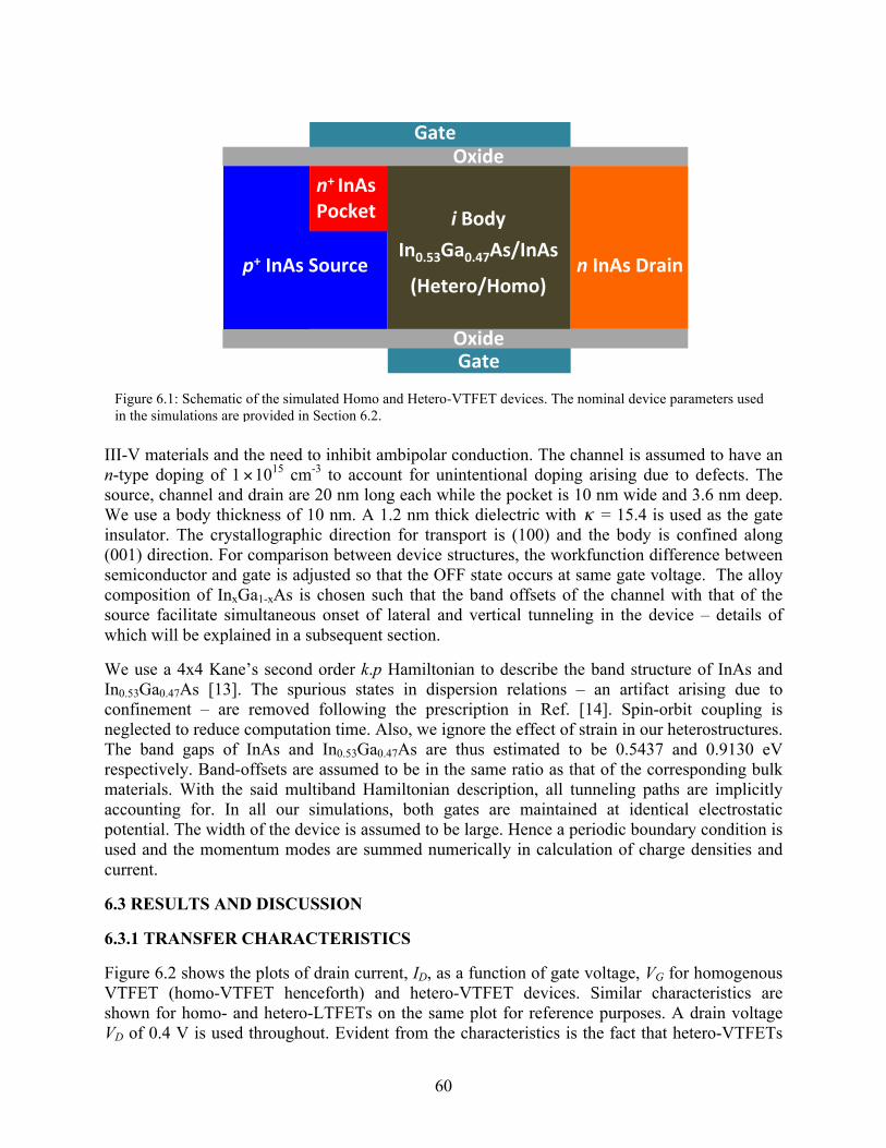
60
III-V materials and the need to inhibit ambipolar conduction. The channel is assumed to have an n-type doping of 1
×1015 cm-3 to account for unintentional doping arising due to defects. The source, channel and drain are 20 nm long each while the pocket is 10 nm wide and 3.6 nm deep. We use a body thickness of 10 nm. A 1.2 nm thick dielectric with
κ = 15.4 is used as the gate insulator. The crystallographic direction for transport is (100) and the body is confined along (001) direction. For comparison between device structures, the workfunction difference between semiconductor and gate is adjusted so that the OFF state occurs at same gate voltage. The alloy composition of InxGa1-xAs is chosen such that the band offsets of the channel with that of the source facilitate simultaneous onset of lateral and vertical tunneling in the device – details of which will be explained in a subsequent section.
We use a 4x4 Kane’s second order k.p Hamiltonian to describe the band structure of InAs and In0.53Ga0.47As [13]. The spurious states in dispersion relations – an artifact arising due to confinement – are removed following the prescription in Ref. [14]. Spin-orbit coupling is neglected to reduce computation time. Also, we ignore the effect of strain in our heterostructures. The band gaps of InAs and In0.53Ga0.47As are thus estimated to be 0.5437 and 0.9130 eV respectively. Band-offsets are assumed to be in the same ratio as that of the corresponding bulk materials. With the said multiband Hamiltonian description, all tunneling paths are implicitly accounting for. In all our simulations, both gates are maintained at identical electrostatic potential. The width of the device is assumed to be large. Hence a periodic boundary condition is used and the momentum modes are summed numerically in calculation of charge densities and current.
6.3 RESULTS AND DISCUSSION
6.3.1 TRANSFER CHARACTERISTICS
Figure 6.2 shows the plots of drain current, ID, as a function of gate voltage, VG for homogenous VTFET (homo-VTFET henceforth) and hetero-VTFET devices. Similar characteristics are shown for homo- and hetero-LTFETs on the same plot for reference purposes. A drain voltage VD of 0.4 V is used throughout. Evident from the characteristics is the fact that hetero-VTFETs
Figure 6.1: Schematic of the simulated Homo and Hetero-VTFET devices. The nominal device parameters used in the simulations are provided in Section 6.2.
!!"#$%&"'()*+,"
"!"#$%&"-(+.,/"
""#$%&"0*12$"
#"3(45"
61/,!!
61/,!!
7824,"
7824,"
#$9:;<619:=>%&?#$%&"
@A,/,*(?A(B(C"

61
provide significant reduction in OFF state leakage as compared to their homogenous counterparts. They also provide much steeper subthreshold swings (a minimum SS of 16 mV/decade vs. 62 mV/decade in homo-VTFETs). Although a reduction in ON current as expected is observed due to staggered bands at the heterojunction, the pocket geometry, by virtue of boosting the current due to vertical tunneling, reduces this penalty in comparison to LTFETs. We also note that the advantages of vertical geometry are more pronounced in case of heterojunction devices.
6.3.2 OFF STATE BEHAVIOR
The OFF state behavior of a hetero-VTFET can be understood by examining the energy band diagram and energy resolved current, I(E) (= T(E)
× (f1(E)-f2(E)) where T(E) is the transmission coefficient at a given energy E and f1 and f2 the Fermi Dirac distributions corresponding to source and drain electrochemical potentials respectively), plotted in Fig. 6.3 for both homo- and hetero-VTFETs. The smaller OFF state leakage in hetero-VTFETs is due to two reasons – (i) larger barrier height due to band discontinuities and (ii) larger effective mass m* in the channel (0.046m0 at the bottom of conduction band in In0.53Ga0.47As versus 0.032m0 in InAs, m0 being the free electron mass) implying a smaller wavefunction penetration.
6.3.3 TURN-ON MECHANISM
We now turn to explain a fundamental difference in the turn-on mechanism of a VTFET in comparison to that of an LTFET. Intuitively, the heterojunction VTFET can be visualized in the
Figure 6.2: ID – VG characteristics of homo- and hetero-VTFETs at VD = 0.4 V. Similar characteristics are shown for the case of hetero-LTFET for comparison sake. The hetero-LTFET has top-gate extending over the body alone. The steepest SS obtained in case of Homo and Hetero-VTFETs are 62 mV/decade (from VG = 0.375 V to 0.4 V) and 16 mV/decade (from VG = 0.575 V to 0.6 V) respectively. The black and green curves in (b) are identical to blue and black curves respectively from the previous chapter, except for a shift in OFF state voltage done for comparison purposes.
! !"# $
$!!%
$!!&
$!!
'()*'+
, -)*./0µ.+
Hetero VTFET Hetero LTFET
60 mV/dec
Homo LTFET Homo VTFET

62
pocket region as in Fig. 6.4(a) i.e., as a heterojunction MOSFET with its source being a p+-n+
tunnel diode that creates a non-equilibrium (non-Fermi-Dirac) distribution of carriers in contrast with a conventional, equilibriated source. We plot, as in Fig. 6.4(b), the self-consistent potential profiles along the length of the device in hetero-VTFET near the semiconductor/top-gate-
Figure 6.3: (a) Energy band diagrams in homo- and hetero-VTFETs at z = 0 (semiconductor- top gate insulator interface) at VG = 0.25 V which corresponds to OFF state. (b) The corresponding energy resolved current I(E).
! "! #! $!
!%
!!&'
!
!&'
%
()*+,-
.+/012)*/3-
Hetero VTFET
Homo VTFET
(a)
!"!!#
!"!!"
!"!$
!"%&
!"%'
!"%(
!"%#
!"%!
"
)*+,-./0+12
30)2/04%5%2
Hetero VTFET
Homo VTFET
(b)
Figure 6.4: (a) Schematic band diagram from source to drain in the pocket region depicting the reason for uniqueness of turn-on in hetero-VTFETs. (b) Simulated energy band diagrams in hetero-VTFET at z = 0 for three gate voltages in the region of steepest turn-on. The inset has the same zoomed in the pocket-channel interface region. The arrow in the inset shows the energy window where majority of tunneling current flows. (c) I(E) in hetero-VTFET for same gate voltages as in (b).
p+ - n+
Tunnel diode Heterojunction MOSFET
Drain Channel
Non-
equilibrium
MOSFET
source
Equilibrated
Source
Gate
(a)
!" #" $" %" &" '"
!!
!"(&
"
"(&
!
)*+,-.
/,0123*+04.
! "# "! $# $!
!#%$
!#%&
!#%"
#
#%"
'()*+,
-*./01().2,
VG = 0.55 V
VG = 0.575 V
Barrier height
modulation
VG = 0.6 V
(b)
!"!#
!"!$
!"!%
!"&!
!"&"'
!"&"(
"&"(
)*+,-*.&/&,
+01234-*15,
VG = 0.55 V
VG = 0.575 V
VG = 0.6 V
(c)

63
insulator interface for three different gate voltages in the region where the turn-on is the steepest. We note that this corresponds to the transition wherein the peak in I(E) – shown for corresponding gate voltages in Fig. 6.4(c) – moves from below the barrier at the heterojunction to above it. It can be seen, from the inset of Fig. 6.4(b), that the tunneling width in the energy window where most of the current flows, remains virtually unchanged during this transition. This is in stark contrast to the case of switching in LTFET, where it is primarily the tunnel-barrier width and not height that is modulated. Two important clarificatory points are in order here – (i) the steepness is not sensitive to the sharpness of the barrier at the heterojunction and any broadening of this barrier – for example, one introduced by scattering – will manifest only as a shift in the turn-on voltage. This is due to the fact that the p+-n+ tunnel junction at the source-pocket interface is always turned on, by virtue of doping, as can be seen in Fig. 6.4(b); (ii) while the switching mechanism could be expected to be similar in a homo-VTFET, the phenomenon is masked because of large lateral tunneling current – akin to LTFET current – that flows underneath the pocket, as is evidenced by the presence of tunneling states in a plot of logarithmic local density-of-states (LDOS) along the length of homo-VTFET, near the semiconductor/back-gate-insulator interface (Fig. 6.5(b)).
6.3.4 FACTORS AFFECTING STEEPNESS
There are two other reasons for greater steepness in turn-on of a hetero-VTFET. First is the onset of lateral tunneling underneath the pocket together with tunneling in the pocket region. Figure 6.5(a) shows logarithmic LDOS plots in hetero-VTFET near the back-gate for VG = 0.55 V and 0.6 V (the interval of steepest switching). We observe that owing to the optimum choice of band discontinuities between source and channel materials, unlike homo-VTFET where the onset of lateral tunneling precedes turn-on in pocket region as explained before, in case of
Figure 6.5: (a) Plots of logarithmic LDOS in hetero-VTFET at z = 10 nm (semiconductor/back-gate-insulator interface) at VG = 0.55 V and 0.6 V. (b) LDOS plot in homo-VTFET at z = 10 nm at VG = 0.375 V. (c) and (d) are LDOS plots along body thickness at x = 15 nm (middle of the pocket region) in homo- (VG = 0.375 V) and hetero- (VG = 0.575 V) VTFETs respectively.
Tunneling
states
Small vertical
tunneling
Large vertical
tunneling
No Tunneling
states in overlap
region
Tunneling states
in source-
channel band
overlap
VG = 0.55 V V
G = 0.6 V
(a)
(b) (c) (d)
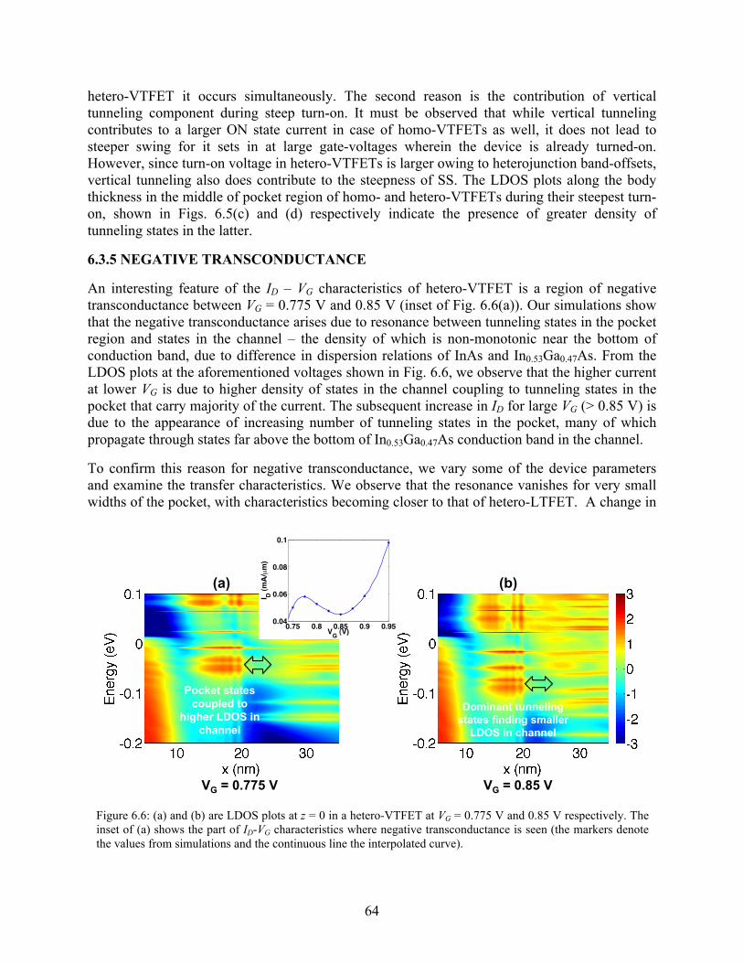
64
hetero-VTFET it occurs simultaneously. The second reason is the contribution of vertical tunneling component during steep turn-on. It must be observed that while vertical tunneling contributes to a larger ON state current in case of homo-VTFETs as well, it does not lead to steeper swing for it sets in at large gate-voltages wherein the device is already turned-on. However, since turn-on voltage in hetero-VTFETs is larger owing to heterojunction band-offsets, vertical tunneling also does contribute to the steepness of SS. The LDOS plots along the body thickness in the middle of pocket region of homo- and hetero-VTFETs during their steepest turn-on, shown in Figs. 6.5(c) and (d) respectively indicate the presence of greater density of tunneling states in the latter.
6.3.5 NEGATIVE TRANSCONDUCTANCE
An interesting feature of the ID – VG characteristics of hetero-VTFET is a region of negative transconductance between VG = 0.775 V and 0.85 V (inset of Fig. 6.6(a)). Our simulations show that the negative transconductance arises due to resonance between tunneling states in the pocket region and states in the channel – the density of which is non-monotonic near the bottom of conduction band, due to difference in dispersion relations of InAs and In0.53Ga0.47As. From the LDOS plots at the aforementioned voltages shown in Fig. 6.6, we observe that the higher current at lower VG is due to higher density of states in the channel coupling to tunneling states in the pocket that carry majority of the current. The subsequent increase in ID for large VG (> 0.85 V) is due to the appearance of increasing number of tunneling states in the pocket, many of which propagate through states far above the bottom of In0.53Ga0.47As conduction band in the channel.
To confirm this reason for negative transconductance, we vary some of the device parameters and examine the transfer characteristics. We observe that the resonance vanishes for very small widths of the pocket, with characteristics becoming closer to that of hetero-LTFET. A change in
Figure 6.6: (a) and (b) are LDOS plots at z = 0 in a hetero-VTFET at VG = 0.775 V and 0.85 V respectively. The inset of (a) shows the part of ID-VG characteristics where negative transconductance is seen (the markers denote the values from simulations and the continuous line the interpolated curve).
Pocket states
coupled to
higher LDOS in
channel
Dominant tunneling
states finding smaller
LDOS in channel
VG = 0.775 V VG = 0.85 V
0.75 0.8 0.85 0.9 0.95
0.06
0.08
0.1
0.04
VG
(V)
I D (
mA
/µm
)
(a) (b)

65
band-offsets alters the voltage range of its occurrence and also the extent – with the phenomenon becoming more pronounced for larger conduction-band-offsets and less so for smaller values. A similar behavior is seen when the channel length is varied. These observations confirm our hypothesis of resonance.
6.4 SUMMARY
Our simulations show that the turn-on in a hetero-VTFET is dominated by the modulation of heterojunction barrier height as opposed to that of tunneling-width. We also demonstrate that by choosing the right band offsets, the steepness of turn-on can be increased owing to – (i) simultaneous onset of tunneling in the pocket and region underneath it, and (ii) contribution from vertical tunneling. The negative transconductance region that can occur in hetero-VTFET characteristics is due to resonant tunneling between states in the pocket and those in the channel. Although in this study we have restricted ourselves to nominal device structures so as to retain our emphasis on underlying physics, we note that enhanced performance can be obtained by optimizing the critical device parameters like heterojunction band-offsets (tuned using Ga mole fraction), pocket width and depth and doping profiles in source and pocket regions, thus fully leveraging the advantages of hetero-VTFETs.
This brings us to the end of our discussion on leveraging tunneling in three-terminal devices for steep switching purposes. In the remaining chapters, our goal would be to use the insights gained in tunneling mechanism to design improved short-channel, top-of-the-barrier devices (MOSFETs) in layered materials for non-digital applications. More specifically, in the next chapter, we focus on engineering tunneling in order to enhance output resistance in graphene FETs and on explaining scaling trends in their cut-off frequencies.
6.5 REFERENCES
[1] W. Y. Choi, B. -G. Park and T. -J. K. Liu, “Tunneling field-effect transistors (TFETs) with subthreshold swing (SS) less than 60 mV/dec,” IEEE Electron Device Lett., vol. 28, no. 8, pp. 743-745, Aug. 2007.
[2] T. Krishnamohan, D. Kim, S. Raghunathan and K. Saraswat, “ Double-gate strained-Ge heterostructures tunneling FET (TFET) with record high drive currents and <60 mV/dec subthreshold slope,” in IEDM Tech. Digest, December 2008, pp. 1-3.
[3] J. Appenzeller, Y. -M. Lin, J. Knoch and P. Avouris, “Band-to-band tunneling in carbon nanotube transistors,” Phys. Rev. Lett., vol 93, no. 19, pp. 196805-196809, 2004.
[4] S. Mookerjea, D. Mohata, R. Krishnan, J. Singh, A. Vallett, A. Ali, T. Mayer, V. Narayanan, D. Schlom, A. Liu and S. Datta, "Experimental Demonstration of 100nm Channel Length In0.53Ga0.47As-based Vertical Inter-band Tunnel Field Effect Transistors (TFETs) for Ultra Low-Power Logic and SRAM Applications,” in IEDM Tech. Digest, 2009, pp. 949-951.
[5] P. Patel, K. Jeon, A. Bowonder and C. Hu, “A Low Voltage Steep Turn-off Tunnel Transistor Design,” in Proc. of SISPAD, 2009, pp. 23-26.

66
[6] A. Bowonder, P. Patel, K. Jeon, J. Oh, P. Majhi, H. -H. Tseng and C. Hu, “Low-voltage green transistor using ultra shallow junction and hetero-tunneling”, in International Workshop on Junction Technology, Shanghai, 2008, pp. 93-96.
[7] K. Ganapathi, Y. Yoon and S. Salahuddin, “Analysis of InAs vertical and lateral band-to-band tunneling transistors: Leveraging vertical tunneling for improved performance,” Appl. Phys. Lett., vol. 97, no. 3, pp. 033504-033506, 2010.
[8] S. Agarwal, G. Klimeck and M. Luisier, “Leakage-Reduction Design Concepts for Low-Power Vertical Tunneling Field-Effect Transistors,” IEEE Electron Device Lett., vol. 31, no. 6, pp. 621-623, June 2010.
[9] E. -H. Toh, G. H. Wang, G. Samudra and Y. -C. Yeo, “Device physics and design of germanium field-effect transistor with source and drain engineering for low power and high performance applications,” J. Appl. Phys., vol. 103, pp. 104504, 2008.
[10] A. S. Verhulst, W.G. Vanderberghe, K. Maex, S. De Gendt, M. M. Heyns and G. Groeseneken, “Complementary Silicon-based Heterostructure Tunnel-FETs With High Tunnel Rates”, IEEE Electron Device Lett., vol. 29, no. 12, pp. 1398-1400, 2008.
[11] O. M. Nayfeh, C. N. Chleirigh, J. Hennessy, L. Gomez, J. L. Hoyt and D. A. Antoniadis, “Design of Tunneling Field-Effect Transistors using Strained-Silicon/Strained-Germanium Type-II Staggered Heterojunctions,” IEEE Electron Device Lett., vol. 29, no. 9, pp. 1074-1076, 2008.
[12] K. Boucart, W. Riess and A. M. Ionescu, “Lateral Strain Profile as Key Technology Booster for All-Silicon Tunnel FETs,” IEEE Electron Device Lett., vol. 30, no. 6, pp. 656-658, 2009.
[13] D. Gershoni, C. H. Henry and G.A. Baraff, “Calculating the optical properties of Multidimensional Heterostructures: Application to the Modeling of Quaternary Quantum Well Lasers,” IEEE J. Quantum Elect., vol. 29, no. 9, pp. 2433-2450, 2008.
[14] B. A. Foreman, “Elimination of spurious solutions from eight-band k. p theory,” Phys. Rev. B, vol. 56, no. 20, pp. R12748-R12751, 1997.
67
CHAPTER 7
GRAPHENE TRANSISTORS – ENGINEERING TUNNELING TO IMPROVE OUTPUT RESISTANCE In this chapter, we turn our attention to graphene transistors. Graphene, while having attracted a lot of interest in recent times for its unique material properties, remains a challenging system to leverage the advantage of its intrinsic properties. Most of the problems in the domain of electronic devices can be traced back to its gapless nature. Here we focus on two issues that result from band-to-band tunneling in graphene – degraded output resistance and departure in the cut-off frequency scaling trends from expected lines. We propose certain techniques to improve the output resistance and provide interpretations to experimentally observed scaling behavior.
7.1 GRAPHENE TRANSISTORS FOR NON-DIGITAL APPLICATIONS
While the absence of a bandgap and the difficulties in inducing one without substantially degrading its excellent inherent electronic properties – viz. large carrier mobility, mean free path etc. – have rendered graphene less attractive for digital applications, the interest in graphene field-effect transistors for high-frequency RF applications, where transistor turn-off is not critical for device operation, continues [1] - [4]. Although long-channel GFETs have shown some quasi-saturation behavior in their output i.e., IDS – VDS, (IDS and VDS are respectively the drain current and voltages) characteristics, which has been attributed to velocity saturation [5] - [6], this trend is absent in their short-channel counterparts [7], hence resulting in degraded output resistance and subsequently, reduced intrinsic small-signal gain. However, it has been argued, based on the relative density-of-states in the channel vis-à-vis that in the drain, that such quasi-saturation should be observable even in the ballistic limit [8]. Recently, Wang et al. have proposed a technique to separately quantify the effect of velocity saturation and relative density-of-states, both of which might be present in experimental long-channel output characteristics, through symmetric biasing of source and drain [9]. Also, more interestingly, three-terminal negative differential resistance (NDR) has recently been reported in graphene devices of channel lengths varying from 80 to 500 nm [10]. We note that, previously, G. Fiori had predicted the observation of NDR in monolayer and bilayer graphene p-n junctions through NEGF simulations [11].
In light of these observations, it becomes interesting and relevant to ask the following questions: a) Can the quasi-saturation observed in ballistic GFET output characteristics be engineered in some way, thereby enhancing output resistance (r0) and intrinsic gain (gmr0)? b) Is there a unified view, based on arguments relating to density-of-states, that can explain the occurrence of both quasi-saturation and NDR? In this chapter, we attempt to answer these questions and, by investigating the factors affecting quasi-saturation through ballistic NEGF simulations, show that doping the graphene channel in the gate-drain underlap region can significantly enhance the extent of the quasi-saturation region. We also provide reasons, based on our simulation results, for observing either quasi-saturation or NDR – depending on appropriate biasing and doping conditions. Finally, we study the effect of short-channel behavior on transfer characteristics and its implications on transistor intrinsic cut-off frequency (fT), another important figure-of-merit (FOM) in determining the performance in analog applications. By investigating its scaling
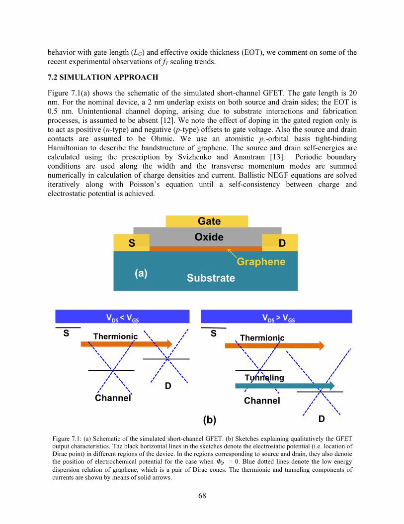
68
behavior with gate length (LG) and effective oxide thickness (EOT), we comment on some of the recent experimental observations of fT scaling trends.
7.2 SIMULATION APPROACH
Figure 7.1(a) shows the schematic of the simulated short-channel GFET. The gate length is 20 nm. For the nominal device, a 2 nm underlap exists on both source and drain sides; the EOT is 0.5 nm. Unintentional channel doping, arising due to substrate interactions and fabrication processes, is assumed to be absent [12]. We note the effect of doping in the gated region only is to act as positive (n-type) and negative (p-type) offsets to gate voltage. Also the source and drain contacts are assumed to be Ohmic. We use an atomistic pz-orbital basis tight-binding Hamiltonian to describe the bandstructure of graphene. The source and drain self-energies are calculated using the prescription by Svizhenko and Anantram [13]. Periodic boundary conditions are used along the width and the transverse momentum modes are summed numerically in calculation of charge densities and current. Ballistic NEGF equations are solved iteratively along with Poisson’s equation until a self-consistency between charge and electrostatic potential is achieved.
Figure 7.1: (a) Schematic of the simulated short-channel GFET. (b) Sketches explaining qualitatively the GFET output characteristics. The black horizontal lines in the sketches denote the electrostatic potential (i.e. location of Dirac point) in different regions of the device. In the regions corresponding to source and drain, they also denote the position of electrochemical potential for the case when ΦB = 0. Blue dotted lines denote the low-energy dispersion relation of graphene, which is a pair of Dirac cones. The thermionic and tunneling components of currents are shown by means of solid arrows.
Substrate
S
Gate
Oxide
Graphene
D
Thermionic S
Channel
D
!"#$%$!&#$
Thermionic S
Channel
D
!"#$'$!&#$
Tunneling
(b)
(a)
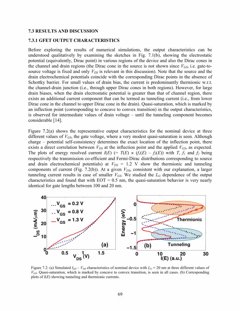
69
7.3 RESULTS AND DISCUSSION
7.3.1 GFET OUTPUT CHARACTERISTICS
Before exploring the results of numerical simulations, the output characteristics can be understood qualitatively by examining the sketches in Fig. 7.1(b), showing the electrostatic potential (equivalently, Dirac point) in various regions of the device and also the Dirac cones in the channel and drain regions (the Dirac cone in the source is not shown since VGS, i.e. gate-to-source voltage is fixed and only VDS is relevant in this discussion). Note that the source and the drain electrochemical potentials coincide with the corresponding Dirac points in the absence of Schottky barrier. For small values of drain bias, the current is predominantly thermionic w.r.t. the channel-drain junction (i.e., through upper Dirac cones in both regions). However, for large drain biases, when the drain electrostatic potential is greater than that of channel region, there exists an additional current component that can be termed as tunneling current (i.e., from lower Dirac cone in the channel to upper Dirac cone in the drain). Quasi-saturation, which is marked by an inflection point (corresponding to concave to convex transition) in the output characteristics, is observed for intermediate values of drain voltage – until the tunneling component becomes considerable [14]. Figure 7.2(a) shows the representative output characteristics for the nominal device at three different values of VGS, the gate voltage, where a very modest quasi-saturation is seen. Although charge – potential self-consistency determines the exact location of the inflection point, there exists a direct correlation between VDS at the inflection point and the applied VGS, as expected. The plots of energy resolved current I(E) (= T(E) × (f1(E) – f2(E)) with T, f1 and f2 being respectively the transmission co-efficient and Fermi-Dirac distributions corresponding to source and drain electrochemical potentials) at VDS = 1.2 V show the thermionic and tunneling components of current (Fig. 7.2(b)). At a given VDS, consistent with our explanation, a larger tunneling current results in case of smaller VGS. We studied the LG dependence of the output characteristics and found that with EOT = 0.5 nm, the quasi-saturation behavior is very nearly identical for gate lengths between 100 and 20 nm.
Figure 7.2: (a) Simulated IDS – VDS characteristics of nominal device with LG = 20 nm at three different values of VGS. Quasi-saturation, which is marked by concave to convex transition, is seen in all cases. (b) Corresponding plots of I(E) showing tunneling and thermionic currents.
0 0.5 1 1.50
10
20
30
40
VDS
(V)
I DS (
mA
/µm
)
VGS
= 0.2 V
VGS
= 0.8 V
VGS
= 1.3 V
! "! #! $!
!"%&
!"
!!%&
!
'()*+(,%-%*
)./012+(/3*
Tunneling
Thermionic
(a) (b)
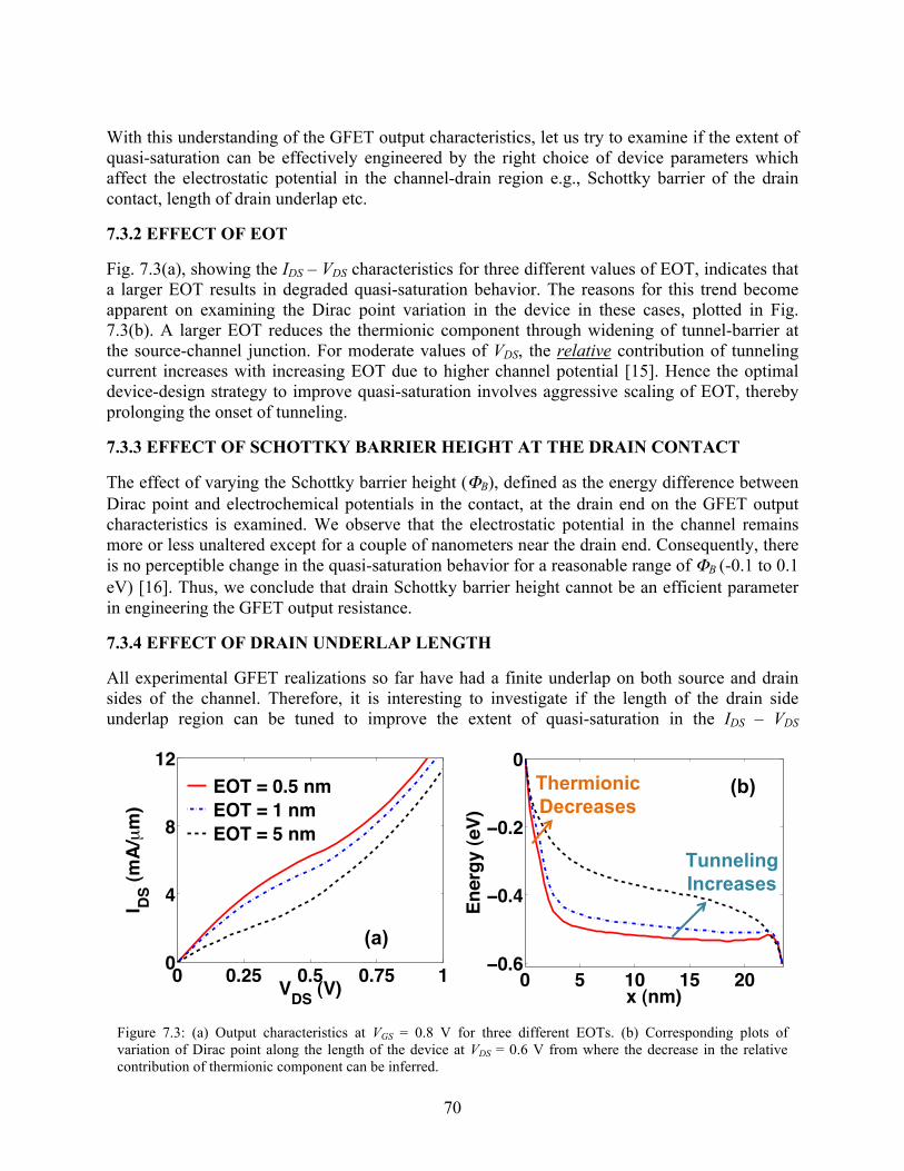
70
With this understanding of the GFET output characteristics, let us try to examine if the extent of quasi-saturation can be effectively engineered by the right choice of device parameters which affect the electrostatic potential in the channel-drain region e.g., Schottky barrier of the drain contact, length of drain underlap etc.
7.3.2 EFFECT OF EOT
Fig. 7.3(a), showing the IDS – VDS characteristics for three different values of EOT, indicates that a larger EOT results in degraded quasi-saturation behavior. The reasons for this trend become apparent on examining the Dirac point variation in the device in these cases, plotted in Fig. 7.3(b). A larger EOT reduces the thermionic component through widening of tunnel-barrier at the source-channel junction. For moderate values of VDS, the relative contribution of tunneling current increases with increasing EOT due to higher channel potential [15]. Hence the optimal device-design strategy to improve quasi-saturation involves aggressive scaling of EOT, thereby prolonging the onset of tunneling.
7.3.3 EFFECT OF SCHOTTKY BARRIER HEIGHT AT THE DRAIN CONTACT
The effect of varying the Schottky barrier height (ΦB), defined as the energy difference between Dirac point and electrochemical potentials in the contact, at the drain end on the GFET output characteristics is examined. We observe that the electrostatic potential in the channel remains more or less unaltered except for a couple of nanometers near the drain end. Consequently, there is no perceptible change in the quasi-saturation behavior for a reasonable range of ΦB (-0.1 to 0.1 eV) [16]. Thus, we conclude that drain Schottky barrier height cannot be an efficient parameter in engineering the GFET output resistance.
7.3.4 EFFECT OF DRAIN UNDERLAP LENGTH
All experimental GFET realizations so far have had a finite underlap on both source and drain sides of the channel. Therefore, it is interesting to investigate if the length of the drain side underlap region can be tuned to improve the extent of quasi-saturation in the IDS – VDS
Figure 7.3: (a) Output characteristics at VGS = 0.8 V for three different EOTs. (b) Corresponding plots of variation of Dirac point along the length of the device at VDS = 0.6 V from where the decrease in the relative contribution of thermionic component can be inferred.
0 0.25 0.5 0.75 10
4
8
12
VDS
(V)
I DS (
mA
/µm
)
EOT = 0.5 nm
EOT = 1 nm
EOT = 5 nm
! " #! #" $!!!%&
!!%'
!!%$
!
()*+,-
.+/012)*/3-
Tunneling
Increases
Thermionic
Decreases
(a)
(b)

71
characteristics. Figure 7.4(a) shows the output characteristics for four different lengths of the drain underlap – 0, 2, 4, and 6 nm [17]. Evidently, with a larger underlap, the saturation behavior is worsened. The reasons are twofold –
(i) For small to intermediate drain voltages, the thermionic component of current decreases with increase in underlap length due to (a) reduced band-bending in the gated region and (b) the presence of higher potential barrier (and hence greater quantum-mechanical reflections) in the underlap region, as can be seen from the variation of Dirac point along the device, plotted for three different lengths of underlap, in Fig. 7.4(b).
(ii) Since the potential at the drain end is fixed for a given VDS, larger underlap and consequently a higher barrier therein results in a larger electric field near the drain end. This implies an increase in the field-driven tunneling component of the current. An increase in total current with larger underlap for high drain biases – where tunneling is the dominant mechanism – corroborates with this explanation. Accordingly, we note that increasing underlap length suppresses the thermionic part while amplifying the tunneling contribution, yielding poorer output resistances in the process.
Having identified the effect of potential barrier in the drain underlap on thermionic and tunneling components, we seek to engineer this barrier to alter the quasi-saturation characteristics. One way to do this is either through introduction of fixed charge in the vicinity or via substitutional doping. Although doping 2-D graphene substitutionally remains an area of active research, techniques to dope it n-type (using nitrogen [18]) and p-type (using gold [19]) have been recently demonstrated. In the forthcoming sections, we discuss the effect of such doping on the output characteristics of GFETs. Due to the barrier within 2 nm of underlap in the nominal device being mostly transparent and due to fabrication challenges in selectively doping such narrow region, we consider GFETs with 6 nm underlap on the drain side.
Figure 7.4: (a) Output characteristics at VGS = 0.8 V with varying lengths of drain underlap region – 0, 2, 4, and 6 nm. (b) Corresponding plots of electrostatic potential profiles at VDS = 0.5 V wherein a larger barrier with increasing underlap can be seen.
! "! #!
!!$%
!!$#%
!
&'()*+
,)-./0'(-1+
Larger barrier with
increasing underlap
0 0.25 0.5 0.75 10
4
8
12
VDS
(V)
I DS (
mA
/µm
)
no underlap
2 nm underlap
4 nm underlap
6 nm underlap
(a)
(b)

72
7.3.5 EFFECT OF n-TYPE DOPING IN THE DRAIN UNDERLAP REGION
Figure 7.5(a) shows the IDS – VDS characteristics of GFETs for three different values of uniform doping concentration in the 6 nm long drain underlap region. We notice that the quasi-saturation becomes more pronounced with increasing doping density. This can be understood by examining the logarithmic local density-of-states (LDOS) plotted for a doping density N of 1x1013 cm-2, shown in Fig. 7.5(b). A larger doping concentration reduces the barrier height in the underlap region and in case of very high densities inverts the shape of the potential profile. This serves dual purpose – (i) boost in thermionic current due to reduced barrier in the underlap and enhanced band-bending in the gated region; (ii) blockage of tunneling current due to the presence of potential barrier for holes. In essence, n-type doping has the effect of delaying the onset of tunneling-dominated regime in the output characteristics, resulting in an increase in device output resistance.
7.3.6 EFFECT OF p-TYPE DOPING IN THE DRAIN UNDERLAP REGION
Having appreciated the effect of n-type doping on quasi-saturation, intuitively, it might seem that p-type doping should worsen the output resistance. However, the plot of IDS – VDS characteristics for three different values of doping concentration in Fig. 7.6(a) suggests that p-type doping too enhances the extent of saturation. This is an interesting result and merits detailed discussion. We note that while for increasing values of p-type doping, quasi-saturation behavior progressively improves, for a doping of N = 1x1013 cm-2, improvement in r0 is substantial. This, resulting from larger current at small VDS and smaller current at larger VDS, is because of the following:
The potential barrier in the drain underlap region increases with increasing doping concentration. For N = 1x1013 cm-2, the potential barrier is so high that for small values of drain biases, all the current is because of tunneling through it. This leads to a resonance between the states in the gated-channel and in the barrier region, leading to a current larger than the undoped case. This is
Figure 7.5: (a) IDS – VDS characteristics at VGS = 0.8 V showing the effect of varying n-type doping concentration in the 6 nm drain underlap region. (b) Plot of logarithmic LDOS for the N = 1x1013 cm-2 case at VDS = 0.5 V. The Dirac point inside the channel is also shown in white. The quantum-mechanical reflections above the well are also evident.
0 0.25 0.5 0.75 10
4
8
12
VDS (V)
I DS (m
A/µ
m)
1x1013 cm 2
6.8x1012 cm 2
3.4x1012 cm 2
0
Reflections (b)
(a)
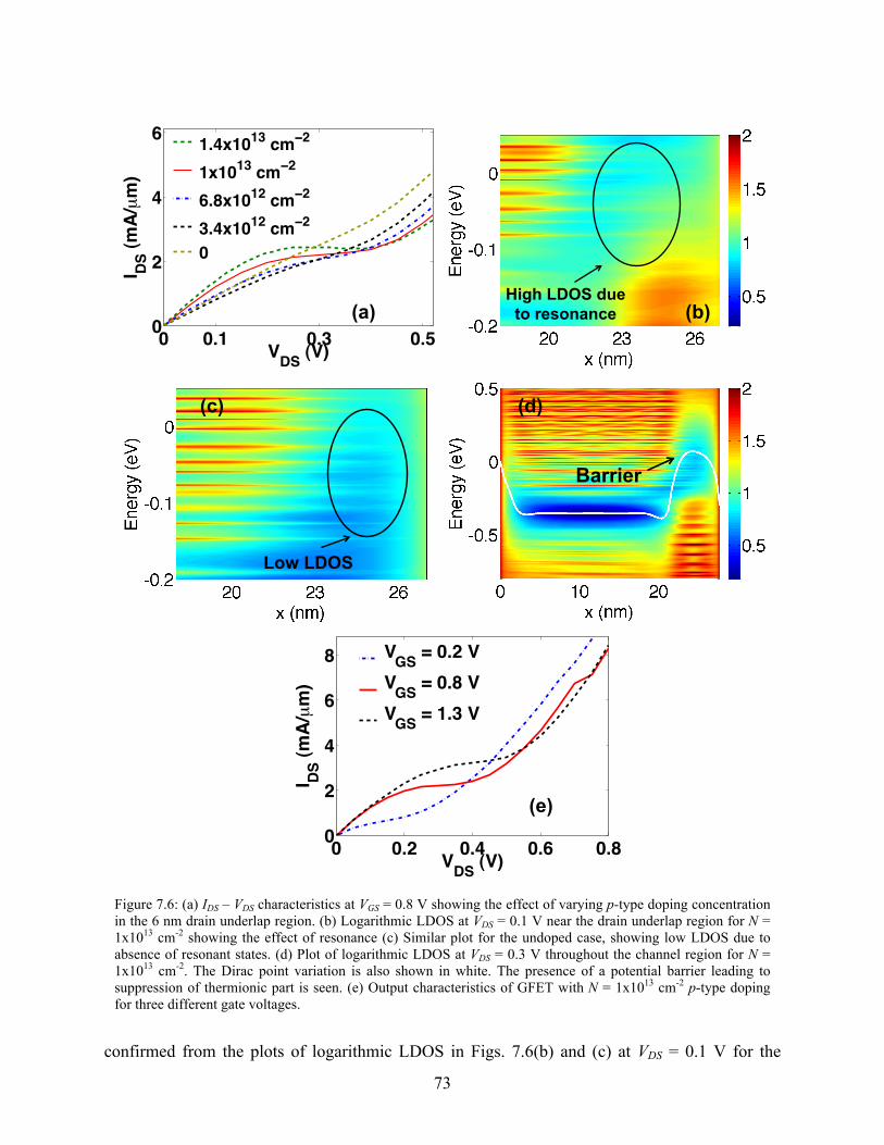
73
confirmed from the plots of logarithmic LDOS in Figs. 7.6(b) and (c) at VDS = 0.1 V for the
Figure 7.6: (a) IDS – VDS characteristics at VGS = 0.8 V showing the effect of varying p-type doping concentration in the 6 nm drain underlap region. (b) Logarithmic LDOS at VDS = 0.1 V near the drain underlap region for N = 1x1013 cm-2 showing the effect of resonance (c) Similar plot for the undoped case, showing low LDOS due to absence of resonant states. (d) Plot of logarithmic LDOS at VDS = 0.3 V throughout the channel region for N = 1x1013 cm-2. The Dirac point variation is also shown in white. The presence of a potential barrier leading to suppression of thermionic part is seen. (e) Output characteristics of GFET with N = 1x1013 cm-2 p-type doping for three different gate voltages.
Low LDOS
! !"# !"$ !"%!
&
'
(
)*+,-).
/ *+,-012µ0.
,#"'3#!#$,40
!&
,#3#!#$,40
!&
,("53#!#&,40
!&
,$"'3#!#&,40
!&
,!
(a)
Barrier
(d)
High LDOS due
to resonance
(c)
(b)
0 0.2 0.4 0.6 0.80
2
4
6
8
VDS
(V)
I DS (
mA
/µm
)
VGS
= 0.2 V
VGS
= 0.8 V
VGS
= 1.3 V
(e)
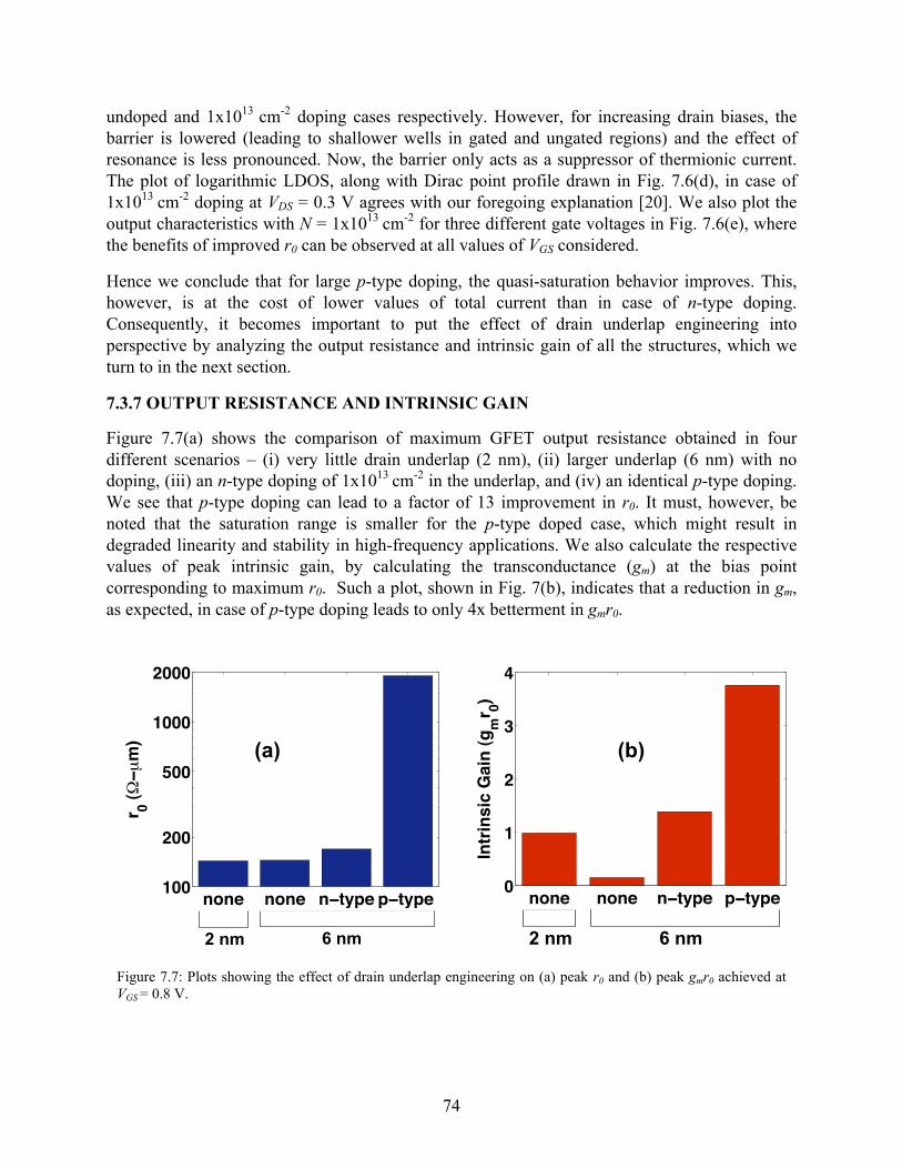
74
undoped and 1x1013 cm-2 doping cases respectively. However, for increasing drain biases, the barrier is lowered (leading to shallower wells in gated and ungated regions) and the effect of resonance is less pronounced. Now, the barrier only acts as a suppressor of thermionic current. The plot of logarithmic LDOS, along with Dirac point profile drawn in Fig. 7.6(d), in case of 1x1013 cm-2 doping at VDS = 0.3 V agrees with our foregoing explanation [20]. We also plot the output characteristics with N = 1x1013 cm-2 for three different gate voltages in Fig. 7.6(e), where the benefits of improved r0 can be observed at all values of VGS considered.
Hence we conclude that for large p-type doping, the quasi-saturation behavior improves. This, however, is at the cost of lower values of total current than in case of n-type doping. Consequently, it becomes important to put the effect of drain underlap engineering into perspective by analyzing the output resistance and intrinsic gain of all the structures, which we turn to in the next section.
7.3.7 OUTPUT RESISTANCE AND INTRINSIC GAIN
Figure 7.7(a) shows the comparison of maximum GFET output resistance obtained in four different scenarios – (i) very little drain underlap (2 nm), (ii) larger underlap (6 nm) with no doping, (iii) an n-type doping of 1x1013 cm-2 in the underlap, and (iv) an identical p-type doping. We see that p-type doping can lead to a factor of 13 improvement in r0. It must, however, be noted that the saturation range is smaller for the p-type doped case, which might result in degraded linearity and stability in high-frequency applications. We also calculate the respective values of peak intrinsic gain, by calculating the transconductance (gm) at the bias point corresponding to maximum r0. Such a plot, shown in Fig. 7(b), indicates that a reduction in gm, as expected, in case of p-type doping leads to only 4x betterment in gmr0.
Figure 7.7: Plots showing the effect of drain underlap engineering on (a) peak r0 and (b) peak gmr0 achieved at VGS = 0.8 V.
!"!# !"!# !!$%&# &!$%&#'())
()))
*))
+))
*)))
, )'-!!!./
2 nm 6 nm 2 nm 6 nm
!"!# !"!# !!$%&# &!$%&#'
(
)
*
+
,!$-.!/.0123.!1456- '7
(a) (b)

75
7.3.8 ARE QUASI-SATURATION AND THREE-TERMINAL NDR RELATED?
Having understood quasi-saturation in GFETs and ways to engineer it, we now explain how it can be related to the three-terminal NDR effect that has been observed in recent experiments [10]. In this regard, the following observations are in order:
(i) In the simulations of our nominal GFETs, we observe quasi-saturation and not NDR. This is due to the fact that for small VDS, we do not have any tunnel barrier inside the channel. The current herein is thermionic and tunneling current onsets only for moderate to large VDS.
(ii) However, situation can be different if for small VDS we have a tunneling barrier in the channel, as in case of large p-type doping. Our simulations with 1.4x1013 cm-2 doping (Fig. 7.6(a)) in the drain underlap indeed exhibit NDR behavior for reasons explained above.
(iii) The three-terminal IDS – VDS characteristics at a given VGS are identical to two-terminal current-voltage characteristics if we regard the effect of VGS is to electrostatically dope the gated region. The ungated (i.e. underlap) region can be considered to be oppositely doped in some cases – including when metal contacts induce doping in their vicinity, as argued in Ref. [21] – when the curvature of potential flips while transitioning between gated and ungated regions. Therefore, it is not inconceivable to think of situations where the electrostatic potential profile in a GFET, biased at fixed VGS, can look like that of a tunnel diode. Hence we believe that the reported three-terminal NDR reported is fundamentally same as the NDR in graphene p+– n+ diodes, predicted in Ref. [11], which in turn is qualitatively identical to similar effect observed in tunnel diodes of conventional semiconductors with finite bandgap [22].
7.3.9 EFFECT OF LG SCALING ON fT
We now turn to understand the scaling trends in fT, which is another important FOM for analog and RF applications. In particular, we first focus on the effect of LG scaling on fT. Figures 7.8(a) and (b) show the IDS – VGS and gm – VGS characteristics respectively for different gate lengths at VDS = 0.4 V when the EOT is 25 nm. The degraded OFF state leakage with reducing LG is due enhanced tunneling owing to larger lateral electric field, in agreement with what has previously been reported in Refs. [23] and [24]. This, coupled with an LG-independent ON current at large gate voltages, leads to reduced gm.
Figure 7.8(c) shows this trend in peak gm, wherein we note that the LG below which gm starts to fall-off and the extent of degradation should both depend on EOT [25]. The intrinsic cut-off frequency (fT = gm/2πCG, CG being the total gate capacitance) is calculated and plotted as a function of LG in Fig. 7.8(d) [26]. We note that while for very small EOTs, an expected 1/LG scaling, in agreement with Ref. [8], is observed, in case of large of EOTs, a significant departure from this behavior is seen due to short-channel behavior. This deviation is different from the one due to parasitic resistances and capacitances reported in Ref. [24]. In view of this result, we make the following comments about the recently reported 1/LG dependence of fT in Ref. [7] (EOT = 38 nm) –
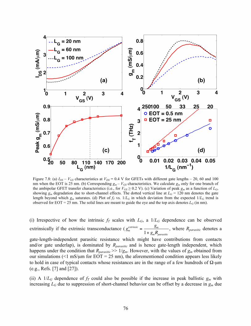
76
(i) Irrespective of how the intrinsic fT scales with LG, a 1/LG dependence can be observed
extrinsically if the extrinsic transconductance (
gmextrinsic =
gm1+ gmRparasitic
, where Rparasitic denotes a
gate-length-independent parasitic resistance which might have contributions from contacts and/or gate underlap), is dominated by Rparasitic and is hence gate-length independent, which happens under the condition that Rparasitic >> 1/gm. However, with the values of gm obtained from our simulations (<1 mS/µm for EOT = 25 nm), the aforementioned condition appears less likely to hold in case of typical contacts whose resistances are in the range of a few hundreds of Ω-µm (e.g., Refs. [7] and [27]).
(ii) A 1/LG dependence of fT could also be possible if the increase in peak ballistic gm with increasing LG due to suppression of short-channel behavior can be offset by a decrease in gm due
Figure 7.8: (a) IDS – VGS characteristics at VDS = 0.4 V for GFETs with different gate lengths – 20, 60 and 100 nm when the EOT is 25 nm. (b) Corresponding gm – VGS characteristics. We calculate gm only for one branch of the ambipolar GFET transfer characteristics (i.e., for VGS ≥ 0.2 V). (c) Variation of peak gm as a function of LG, showing gm degradation due to short-channel effects. The dotted vertical line at LG = 120 nm denotes the gate length beyond which gm saturates. (d) Plot of fT vs. 1/LG in which deviation from the expected 1/LG trend is observed for EOT = 25 nm. The solid lines are meant to guide the eye and the top axis denotes LG (in nm).
0 1 2 3 41
2
3
4
VGS
(V)
I DS (
mA
/µm
)
LG
= 20 nm
LG
= 60 nm
LG
= 100 nm
0 1 2 3 40
0.2
0.4
0.6
0.8
VGS
(V)
gm
(m
S/µ
m)
20 50 80 110 140 170 2000.5
0.6
0.7
0.8
0.9
LG
(nm)
Peak g
m (
mS
/µm
)
! !"!# !"!$ !"!% !"!& !"!'!
#
$
%
&
#()*+,-.
!#/
0 1+,123/
$'!#!! '! %% $' $!
+
451+6+!"'+-.
451+6+$'+-.
(a) (b)
(c) (d)
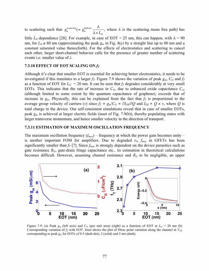
77
to scattering such that
gmscattering(
= gmballistic λ
λ+ LG, where λ is the scattering mean free path) has
little LG dependence [28]. For example, in case of EOT = 25 nm, this can happen, with λ = 90 nm, for LG ≤ 80 nm (approximating the peak gm in Fig. 8(c) by a straight line up to 80 nm and a constant saturated value thenceforth). For the effects of electrostatics and scattering to cancel each other, larger short-channel behavior calls for the presence of greater number of scattering events i.e. smaller value of λ.
7.3.10 EFFECT OF EOT SCALING ON fT
Although it’s clear that smaller EOT is essential for achieving better electrostatics, it needs to be investigated if this translates to a larger fT. Figure 7.9 shows the variation of peak gm, CG and fT as a function of EOT for LG = 20 nm. It can be seen that fT degrades considerably at very small EOTs. This indicates that the rate of increase in CG, due to enhanced oxide capacitance Cox (although limited to some extent by the quantum capacitance of graphene), exceeds that of increase in gm. Physically, this can be explained from the fact that fT is proportional to the average group velocity of carriers (v) since fT ∝ gm/CG ∝ ∂IDS/∂Q and IDS ∝ Q × v, where Q is total charge in the device. Our self-consistent simulations reveal that in case of smaller EOTs, peak gm is achieved at larger electric fields (inset of Fig. 7.9(b)), thereby populating states with larger transverse momentum, and hence smaller velocity in the direction of transport.
7.3.11 ESTIMATION OF MAXIMUM OSCILLATION FREQUENCY
The maximum oscillation frequency (fmax) – frequency at which the power gain becomes unity – is another important FOM for amplifiers. Due to degraded r0, fmax in GFETs has been significantly smaller than fT [7]. Since fmax is strongly dependent on the device parasitics such as gate resistance RG, gate-drain fringe capacitance etc., its estimation in theoretical calculations becomes difficult. However, assuming channel resistance and RG to be negligible, an upper
Figure 7.9: (a) Peak gm (left axis) and CG (per unit area) (right) as a function of EOT at LG = 20 nm (b) Corresponding variation of fT with EOT. Inset shows the plot of Dirac point variation along the channel at VGS corresponding to peak gm for EOTs of 0.5 (dash-dot), 2 (solid) and 5 nm (dash).
0 5 10 15 20 250
2
4
6
EOT (nm)
Peak g
m (
mS
/µm
)
0 5 10 15 20 25
0
1
2
CG
(µ
F/c
m2)
0 5 10 15 20 252.3
2.5
2.7
2.9
3.1
EOT (nm)
f T (
TH
z)
! " #!!!$%
!!$&
!
'()*+,
-*./01().2,
(a) (b)
78
bound on fmax can be given by
fmax ≈fT2
r0Rs
where RS is the source contact resistance [7]. Using
a typical value for RS (= 500 Ω-µm), we estimate fmax for the four cases referred to in Fig. 7.7 to be 690, 110, 900, and 720 GHz respectively.
7.4 SUMMARY
To summarize, using self-consistent ballistic NEGF simulations of short-channel GFETs, we show that (i) the extent of quasi-saturation in the output characteristics can be enhanced by doping the channel in the drain underlap region – a 1x1013 cm-2 of p-type doping leads to 13x and 4x improvement in r0 and gmr0 respectively; (ii) the quasi-saturation and NDR in three-terminal graphene devices are related phenomena – doping and initial bias conditions determine which one will be observed when and (iii) the intrinsic fT of GFETs can deviate from expected 1/LG scaling trend in case of large EOTs due to enhanced band-to-band tunneling in OFF state. Our results identify optimization directions and windows for some of the key FOMs determining performance of GFETs in analog and RF applications – e.g., while a larger EOT reduces transconductance and hence the intrinsic gain, it might result in a larger cut-off frequency. Future studies should focus on understanding the interplay of these factors together with scattering mechanisms – either due to substrate interactions or impurities – to recognize roadblocks, if any, towards effectively engineering GFETs for next-generation high-frequency electronics.
We conclude this chapter by noting that while much of the research in the graphene-electronics community is driven by its large mobility, which reflects in large fT, output resistance is an equally important FOM as it affects fmax. Although we have shown ways to improve r0 in this study, it is also useful to examine similar FOMs in a material-system where the intrinsic r0 itself could be potentially higher due to the presence of bandgap. Monolayer MoS2, discussed in Chapter 3, is one such example that will be our focus in the next chapter.
7.5 REFERENCES
[1] A. K. Geim and K. S. Novoselov, “The rise of graphene,” Nature Mater., vol. 6, no. 3, pp. 183-191, 2007.
[2] P. Avouris, “Graphene: Electronic and Photonic Properties and Devices,” Nano Lett., vol. 10, no. 11, pp. 4285-4294, 2010.
[3] I. Meric, N. Baklitskaya, P. Kim and K. L. Shepard, “RF performance of top-gated, zero-bandgap graphene field-effect transistors,” in IEDM Tech. Digest, 2008, pp. 1-4.
[4] Y. -M. Lin, K. Jenkins, D. Farmer, A. Valdes-Garcia, P. Avouris, C. –Y. Sung, H. –Y. Chiu and B. Ek, "Development of Graphene FETs for High Frequency Electronics,” in IEDM Tech. Digest, 2009, pp.1-4.
[5] I. Meric, M. Y. Han, A. F. Young, B. Ozyilmaz, P. Kim and K. L. Shepard, “Current saturation in zero-bandgap, top-gated graphene field-effect transistors,” Nat. Nanotechnol., vol. 3, pp. 654-659, 2008.
79
[6] J. Chauhan and J. Guo, “High-field transport and velocity saturation in graphene,” Appl. Phys. Lett., vol. 95, no. 2, pp. 023120-023122, 2009.
[7] Y. Wu, Y. –M. Lin, A. A. Bol, K. A. Jenkins, F. Xia, D. B. Farmer, Y. Zhu and P. Avouris, “High-frequency, scaled graphene transistors on diamond-like carbon,” Nature, vol. 472, no. 7341, pp.74-78, 2011.
[8] S. O. Koswatta, A. Valdes-Garcia, M. B. Steiner, Y. –M. Lin and P. Avouris, “Ultimate RF Performance Potential of Carbon Electronics,” IEEE Trans. Microw. Theory, vol. 59, no. 10, pp. 2739-2750, 2011.
[9] H. Wang, A. Hsu, J. Kong, D. A. Antoniadis and T. Palacios, “Impact of Drain-Induced-Minimum-Shift Effect on Current Saturation of Graphene Transistors,” unpublished.
[10] Y. Wu, D. B. Farmer, W. Zhu, S. –J. Han, C. D. Dimitrakopoulos, A. A. Bol, P. Avouris and Y. –M. Lin, “Three-Terminal Graphene Negative Differential Resistance Devices,” ACS Nano, vol. 6, no. 3, pp. 2610-2616, 2012.
[11] G. Fiori, “Negative Differential Resistance in Mono and Bilayer Graphene p-n Junctions,” IEEE Electron Device Lett., vol. 32, no. 10, pp. 1334-1336, 2011.
[12] J. M. Caridad, F. Rosella, V. Bellani, M. Maicas, M. Patrini and E. Diez, “Effects of particle contamination and substrate interaction on the Raman response of unintentionally doped graphene,” J. Appl. Phys., vol. 108, no. 8, p. 084321-084326, 2010.
[13] A. Svizhenko and M. P. Anantram, “Effect of scattering and contacts on current and electrostatics in carbon nanotubes,” Phys. Rev. B, vol. 72, no. 8, pp. 085430-085439, 2005.
[14] We note that this explanation of the IDS – VDS characteristics of GFETs where the channel has zero bandgap, in terms of tunneling and thermionic currents – along the lines of those of a semiconductor with finite bandgap – is equivalent to the density-of-states argument present in the literature (e.g., Ref. [8]).
[15] Note, however, that for these drain biases, the total current is reduced in case of larger EOT due wider barriers at both source-channel and channel-drain junctions.
[16] Too large a value of ΦB results in increased contact resistance, thereby lowering the extrinsic transconductance while too small a ΦB may not be experimentally realizable due to Fermi-level pinning.
[17] In some cases, there might exist some overlap between gate and drain regions. Electrostatically, this should be identical to the case with no underlap due to inability of gate to modulate the electrostatic potential in the drain contact region.
[18] L. Zhao, R. He, K. T. Rim et al., “Visualizing Individual Nitrogen Dopants in Monolayer Graphene,” Science, vol. 333, no. 6045, pp. 999-1003, 2011.
[19] I. Gierz, C. Riedl, U. Starke, C. R. Ast, K. Kern, “Atomic Hole Doping of Graphene,” Nano Lett., vol. 8, no. 12, pp. 4603-4607, 2008.

80
[20] It is important to note that resonance effect described herein is responsible mainly for larger current at small VDS. The increase in r0 is, however, primarily due to the reduced effect of drain bias on the barrier in the underlap – owing to doping. Hence we expect, to the first order, that enhanced r0 should be observed – albeit to a slightly lesser extent – even in the presence of scattering that can smear the effects of resonance out.
[21] R. Grassi, T. Low, A. Gnudi and G. Baccarani, “Contact-induced negative-differential resistance in short-channel graphene FETs,” arXiv: 1208.2156v1 [cond-mat.mes-hall], 2012.
[22] S. M. Sze and K. K. Ng, Physics of Semiconductor Devices. New York: John Wiley and Sons, 2007, ch. 8.
[23] J. Chauhan and J. Guo, “Assessment of high-frequency performance limits of graphene field-effect transistors,” Nano Res., vol. 4, no. 6, pp. 571-579, 2011.
[24] P. Zhao, D. Jena and S. O. Koswatta, “RF performance projections for 2D graphene transistors: Role of Parasitics at the Ballistic transport limit,” in Proc. Dev. Res. Conf., pp. 81-82, June 2011.
[25] K. Ganapathi, Y. Yoon and S. Salahuddin, “Intrinsic Cut-off Frequency in Scaled Graphene Transistors,” arXiv: 1110.6211v1, 2011.
[26] We emphasize that we have, following Ref. [23], calculated the LC oscillation frequency due to kinetic inductance and found it to be larger than our fT values, thus validating the quasi-static approximation implicit in our NEGF formalism.
[27] K. Nagashio, T. Nishimura, K. Kita and A. Toriumi, “Metal/Graphene Contact as a Performance Killer of Ultra-high Mobility Graphene – Analysis of Intrinsic Mobility and Contact Resistance, ” in IEDM Tech. Digest, 2009, pp. 565-568.
[28] The expression for
gmscattering
has been obtained by differentiating with respect to VGS the analogous equation for IDS.

81
CHAPTER 8
MONOLAYER MoS2 TRANSISTORS – APPLICATIONS BEYOND SWITCHING We investigated ways to improve the analog and RF figures-of-merit in graphene transistors in the previous chapter. Here, we take a look at monolayer MoS2 – another layered material – and examine its potential suitability for high voltage, and high frequency applications. Our interest in this material emanates from the fact that larger bandgap translates to higher breakdown voltage and, from our understanding of output characteristics in the ballistic regime from last chapter, larger output resistance.
8.1 MOTIVATION AND SCOPE
Layered material-systems – where anisotropic material properties lead to adjacent layers along a given direction being held together by weak van der Waals interaction, and hence provide pathways to obtaining a single layer of the material – have sustained significant interest in the nanoelectronic-device community primarily due to – (i) their unique and tunable material properties, (ii) excellent electrostatic integrity of the resulting monolayers (ML) and (ii) amenability to CMOS-compatible processing technologies for large-area integration [1], [2]. While in case of graphene – the most well-studied member of the ML family – the absence of bandgap (EG) and difficulties in inducing one without substantially degrading its intrinsic properties, like large carrier mobility, have resulted in its investigation for analog applications where transistor turn-off is not critical, other materials have gained prominence in the recent years – transition-metal dichalcogenides, hexagonal boron nitride to name a few – due to the presence of finite bandgap even at ML thicknesses [3], [4]. More specifically, ML-MoS2 transistors, where the channel has a bandgap of 1.8 eV, have been shown to exhibit large ON-OFF ratios and excellent subthreshold characteristics in both simulations and experiments [5], [6].
Two-dimensional materials with large EG open up several interesting possibilities in addition to switching applications for which they are already being widely investigated. Important among them are ones requiring high voltage operation such as RF power amplifiers (PA) where large output impedance and power gain are crucial [7]. Although CMOS PAs suffer from issues such as low breakdown voltage (Vbr) and current driving capabilities, III-V-based systems – GaAs devices during early years and more recently by III-nitride high electron-mobility transistors (HEMTs) – which have traditionally dominated this area with their excellent characteristics such as high Vbr as well as large cut-off and maximum oscillation frequencies (fT and fmax), face cost and compatibility with CMOS process-flow as major challenges [8]-[10]. Also, while graphene for high-frequency RF electronics is an area of active research, severely degraded output resistance (r0) – a consequence of lack of bandgap – resulting in low values of fmax poses several fundamental issues at the device-engineering level [11], [12]. We would like to point out that although thermal conductivity and electron mobility – properties crucial for performance in high-power and high frequency devices in diffusive regime i.e., in long-channel transistors – are relatively low for bulk-MoS2, significantly large thermal conductivity in graphene as compared to graphite and reduced significance of concepts like low-field mobility in predicting device

82
behavior at ultra- small channel-lengths give us reasons to be optimistic in case of ML-MoS2 [13], [14]. In light of these considerations, and given the unique advantages systems like ML-MoS2 have to offer, it is instructive to examine their potential as next-generation technologies for aforementioned applications.
In this chapter, we address this issue using self-consistent ballistic quantum transport simulations of short-channel ML-MoS2 FETs within the non-equilibrium Green’s function (NEGF) formalism. In the past, modeling of this system has been limited to Hamiltonian description using an effective mass approximation (at the bottom of conduction band) to the electronic structure obtained from first-principles calculations, thereby shedding light on only unipolar (electron) transport – either through self-consistent simulations or using a top-of-the-barrier model [5], [15]. However, simulation of breakdown characteristics invariably requires description of valence band in addition to that of conduction band in order to capture band-to-band tunneling at the channel-drain junction in the breakdown regime. Also, such prescription enables accurate determination of maximum achievable ON-OFF ratio (i.e., limited by gate-induced drain leakage (GIDL)) in short-channel ML-MoS2 transistors, which has not been explored previously.
We, therefore, develop a 2-band k.p bandstructure model for the ML-MoS2 system and use it in our simulations to answer these questions. It must be noted that although first-principles calculations of electronic structure of ML-MoS2, which have reported a prominent effect of d-electrons in MoS2, in general, provide a more accurate representation than a k.p Hamiltonian – which is known to fit well only in the vicinity of a certain point in the Brillouin zone, and the inability of whose 2-band version in fitting both conduction and valence band effective masses has been well documented – we choose the latter, guided by the following: (i) the drain voltage at onset of breakdown and the tunneling current therein depends, to the first-order, on EG and the reduced effective mass (mr), both of which can be fitted using 2-band k.p, and (ii) computational accuracy – important in later stages of device engineering and optimization – can be traded-off to a certain degree for considerable gain in simulation time, particularly in feasibility studies [16]-[18]. Our results show that in several of the figures-of-merit relevant for beyond-digital applications, ML-MoS2 transistors are comparable or significantly better than similar graphene FETs.
8.2 SIMULATION APPROACH
8.2.1 A TWO-BAND k.p HAMILTONIAN DESCRIPTION OF MONOLAYER MoS2
Our focus here is to obtain an expression for H in the neighborhood of K point of the BZ, where ab-initio studies have shown the existence of bandgap. To this end, we follow a prescription along the lines of Ref. [19], motivated by the fact that the in-plane 120-degree rotational symmetry of ML-MoS2 is identical to that of graphene. Following this, in terms of the in-plane wave vector
k ,
H( k ) can be written as –
(1)
!
H(! k ) =
EG +"2! k 2
2m+"ky p
m
"kx p
m
"kx p
m
"2! k 2
2m""ky p
m
#
$
% % % % %
&
'
( ( ( ( (

83
Here kx and ky denote respectively the component of along K ΓΓ and along a direction perpendicular to it, p is a fitting parameter given by p = (m/2)
× (EG/mr)1/2 and m denotes the free electron mass. The reduced effective mass mr is given by mr = mcmv / (mc + mv) where mc and mv are the conduction and valence band effective masses at the band extrema, calculated to be 0.45m and 0.54m respectively from the bandstructure reported in Ref. [20]. The electronic dispersion relations obtained by diagonalizing
H( k ) are shown in Fig. 8.1. We note that owing
to the lack of adequate number of fitting parameters, error in fitting the larger of mc and mv (mv in our case) is considerably large. However, since our motivation primarily is in determination of Vbr, this would not be a cause for concern as long as a continuous distribution of states is ensured by the Hamiltonian description in the valence band for energies of our interest.
8.2.2 GEOMETRY AND OTHER PARAMETERS
The schematic of the simulated device is shown in Fig. 8.2. The device dimensions and other relevant parameters are mentioned in the caption. The direction of transport is assumed to be along (100). The real-space representation of H therein is obtained by taking the inverse Fourier
! k
Figure 8.1: (a) Bandstructure of ML-MoS2 centered at k = K and along [100] and [010] directions, obtained from the eigenvalues of two-band k.p Hamiltonian described by (1).
!!"# !!"$ ! !"$ !"#!!"%
!
!"%
$
$"%
#
#"%
&!!'($!!)''''''''''''''''''(!$!)'!!*
+,-./0'1-23
Figure 8.2: Schematic of the simulated ML-MoS2 MOSFET. The EOT and gate length are respectively 0.6 and 20 nm. The underlap on the source and drain sides is 2 nm each. Interactions with the substrate are ignored.
Substrate
Source
Gate
Oxide
Monolayer MoS2
Drain

84
transform of
H( k ) and projecting it on to a finite-difference grid. We note that choosing the
optimal grid spacing is more involved than in case of single-band effective mass, because too fine a grid leads to spurious states in the bandgap owing to extension of k.p Hamiltonian to large values of
k where its validity diminishes. With these considerations, the grid spacing is chosen
to be 3.16 Å. The mode-space representation is retained along ky. The source and drain contacts are assumed to be metallic with a small n-type Schottky barrier of 0.1 eV with ML-MoS2, in accordance with experiments [5]. In the calculation of contact self-energies, the metallic Hamiltonian is assumed to be similar to (1), but EG therein is set to zero and p is used as a fitting parameter to obtain injection into the device at all energies of our interest. Ballistic NEGF equations are solved self-consistently with Pöisson’s equation, with charge and current being calculated by summing the contribution from various transverse momentum modes.
8.3 RESULTS AND DISCUSSION
8.3.1 TRANSFER CHARACTERISTICS
Figure 8.3(a) shows the transfer (IDS – VGS) characteristics at a drain voltage (VDS) of 0.4 V on logarithmic and linear scales. In addition to the ideal 60 mV/decade subthreshold swing owing to excellent electrostatic integrity, we observe more than 9 orders of magnitude variation in drain current – a direct manifestation of the large bandgap in ML-MoS2 setting GIDL current limit low [21]. Also, the linear plot reveals a square-law variation of IDS with VGS – an observation return to subsequently.
8.3.2 OUTPUT CHARACTERISTICS
Figure 8.3(b) shows the output (IDS – VDS) characteristics for VGS ≥ 0, which exhibit well-defined saturation behavior over a wide range of drain voltages. This observation is in stark contrast with the case of graphene – where the absence of EG results in sharp degradation in r0 in spite of similar electrostatics [22]. The intrinsic gain and linearity of ML-MoS2-based amplifiers would, consequently, be significantly better.
The output characteristics for VGS < 0 are shown in Fig. 8.3(c), where a clear breakdown behavior – marked by abrupt increase in IDS from its saturated value – is observed for large VDS. This is due to the onset of band-to-band tunneling at the gate-drain junction, as shown in the logarithmic local-density-of-states (LDOS) plot in Fig. 8.3(d) where tunneling states are prominently seen. Because of the small EOT (0.6 nm) used, the drain-to-gate voltage at the onset of breakdown in each case is approximately equal to EG/q (q being the elementary charge); the drain current at breakdown, however, is expectedly VDS-dependent.
8.3.3 CAPACITANCE CHARACTERISTICS
As a first step towards understanding the square-law dependence of IDS on VGS, we examine the
variation of gate-to-source capacitance per unit width, CGS (=
∂Qch
∂VGS VDS =0with Qch being total
channel charge), with VGS at equilibrium (VDS = 0), as shown in Fig. 8.4(a). In addition to the magnitude of CGS being smaller than the oxide capacitance (Cox) – indicating operation close to quantum capacitance regime – a linear dependence on VGS is observed. Noting that quantum
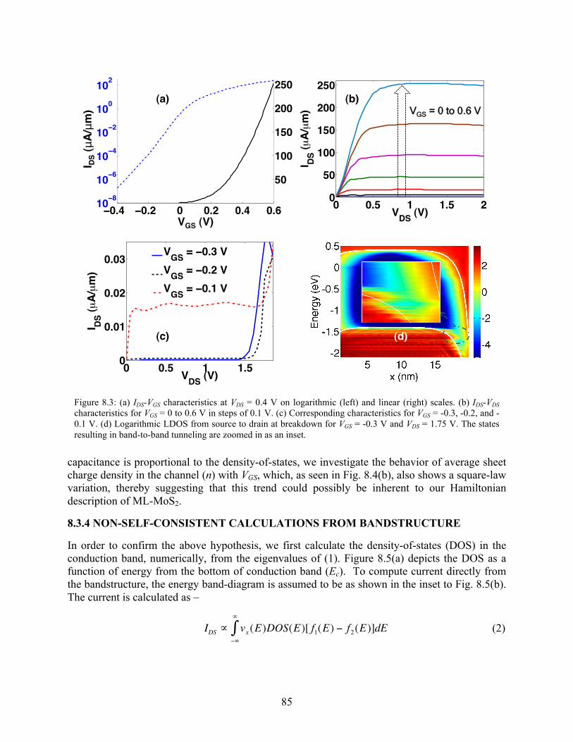
85
capacitance is proportional to the density-of-states, we investigate the behavior of average sheet charge density in the channel (n) with VGS, which, as seen in Fig. 8.4(b), also shows a square-law variation, thereby suggesting that this trend could possibly be inherent to our Hamiltonian description of ML-MoS2.
8.3.4 NON-SELF-CONSISTENT CALCULATIONS FROM BANDSTRUCTURE
In order to confirm the above hypothesis, we first calculate the density-of-states (DOS) in the conduction band, numerically, from the eigenvalues of (1). Figure 8.5(a) depicts the DOS as a function of energy from the bottom of conduction band (Ec). To compute current directly from the bandstructure, the energy band-diagram is assumed to be as shown in the inset to Fig. 8.5(b). The current is calculated as –
IDS ∝ vx (E)DOS(E)[ f1(E) − f2−∞
∞
∫ (E)]dE (2)
Figure 8.3: (a) IDS-VGS characteristics at VDS = 0.4 V on logarithmic (left) and linear (right) scales. (b) IDS-VDS characteristics for VGS = 0 to 0.6 V in steps of 0.1 V. (c) Corresponding characteristics for VGS = -0.3, -0.2, and -0.1 V. (d) Logarithmic LDOS from source to drain at breakdown for VGS = -0.3 V and VDS = 1.75 V. The states resulting in band-to-band tunneling are zoomed in as an inset.
0 0.5 1 1.5 20
50
100
150
200
250
VDS
(V)
I DS (µ
A/µ
m) VVGGSS == 00 ttoo 00..66 VV
! !"# $ $"#!
!"!$
!"!%
!"!&
'()*+',
- ()*+µ./µ0,
'1)*2*!!"&*'
'1)*2*!!"%*'
'1)*2*!!"$*'
!!"# !!"$ ! !"$ !"# !"%&!
!'
&!!%
&!!#
&!!$
&!!
&!$
(!
&!!
&(!
$!!
$(!
VGS (V)!
I DS (!
A/!
m)!
(a)! (b)!
(c)! (d)!
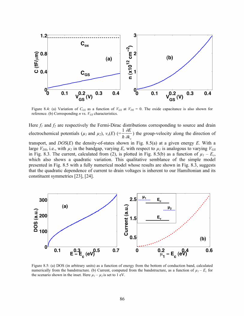
86
Here f1 and f2 are respectively the Fermi-Dirac distributions corresponding to source and drain
electrochemical potentials (µ1 and µ2), vx(E) (=
1∂E∂kx
) the group-velocity along the direction of
transport, and DOS(E) the density-of-states shown in Fig. 8.5(a) at a given energy E. With a large VDS, i.e., with µ2 in the bandgap, varying Ec with respect to µ1 is analogous to varying VGS in Fig. 8.3. The current, calculated from (2), is plotted in Fig. 8.5(b) as a function of µ1 – Ec, which also shows a quadratic variation. This qualitative semblance of the simple model presented in Fig. 8.5 with a fully numerical model whose results are shown in Fig. 8.3, suggests that the quadratic dependence of current to drain voltages is inherent to our Hamiltonian and its constituent symmetries [23], [24].
Figure 8.4: (a) Variation of CGS as a function of VGS at VDS = 0. The oxide capacitance is also shown for reference. (b) Corresponding n vs. VGS characteristics.
0 0.1 0.2 0.3 0.40
0.4
0.8
1.2
VGS
(V)
C (
fF/µ
m)
Cox!
CGS!
(a)
! !"# !"$ !"% !"&!
#
$
%
'()*+',
-*+.#!#$*/0!$,
(b)
Figure 8.5: (a) DOS (in arbitrary units) as a function of energy from the bottom of conduction band, calculated numerically from the bandstructure. (b) Current, computed from the bandstructure, as a function of µ1 – Ec for the scenario shown in the inset. Here µ1 – µ2 is set to 1 eV.
!"# !"$ !"% !"&!
#!!
'!!
$!!
()!)(*)+,-.
/01)+2"3".
! !"# !"$ !"%
!"&
'"&
#"&
µ'(!()
*(+,-.
/011,23(+4"0".
!1"
!2"
Ec"
Ev"
(a)!
(b)!
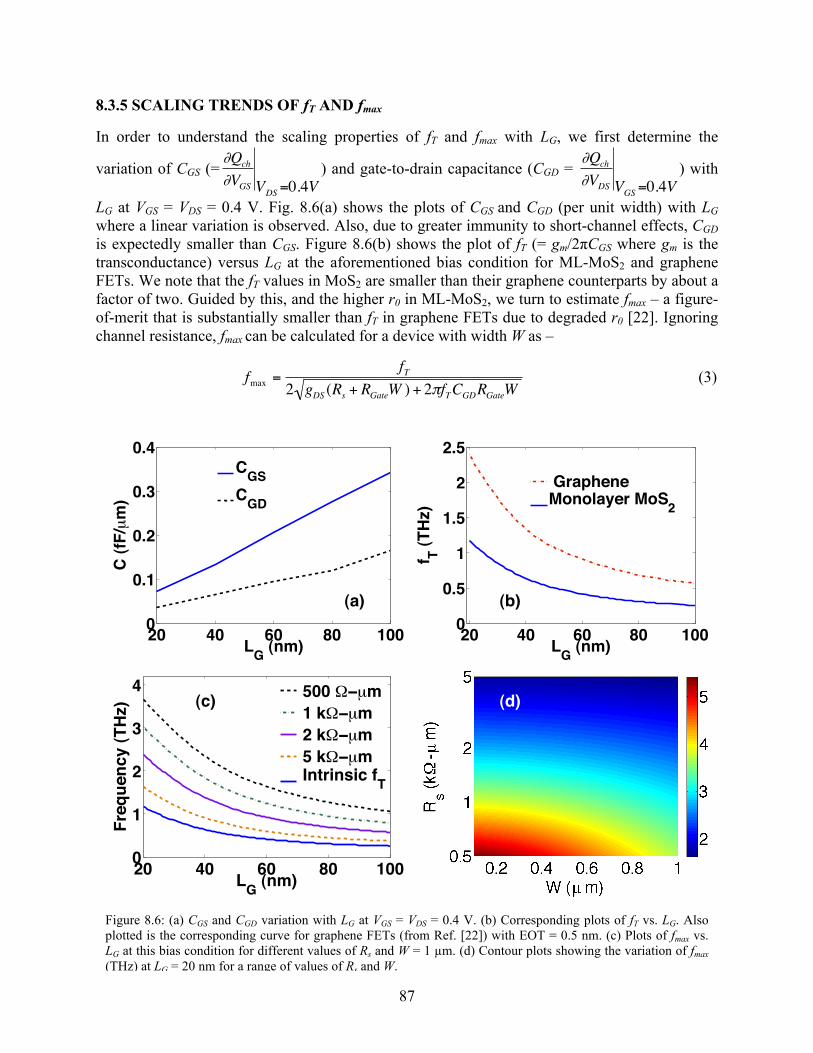
87
8.3.5 SCALING TRENDS OF fT AND fmax
In order to understand the scaling properties of fT and fmax with LG, we first determine the
variation of CGS (=
∂Qch
∂VGS VDS =0.4V) and gate-to-drain capacitance (CGD =
∂Qch
∂VDS VGS =0.4V) with
LG at VGS = VDS = 0.4 V. Fig. 8.6(a) shows the plots of CGS and CGD (per unit width) with LG where a linear variation is observed. Also, due to greater immunity to short-channel effects, CGD is expectedly smaller than CGS. Figure 8.6(b) shows the plot of fT (= gm/2πCGS where gm is the transconductance) versus LG at the aforementioned bias condition for ML-MoS2 and graphene FETs. We note that the fT values in MoS2 are smaller than their graphene counterparts by about a factor of two. Guided by this, and the higher r0 in ML-MoS2, we turn to estimate fmax – a figure-of-merit that is substantially smaller than fT in graphene FETs due to degraded r0 [22]. Ignoring channel resistance, fmax can be calculated for a device with width W as –
fmax =fT
2 gDS (Rs + RGateW ) + 2πfTCGDRGateW (3)
Figure 8.6: (a) CGS and CGD variation with LG at VGS = VDS = 0.4 V. (b) Corresponding plots of fT vs. LG. Also plotted is the corresponding curve for graphene FETs (from Ref. [22]) with EOT = 0.5 nm. (c) Plots of fmax vs. LG at this bias condition for different values of Rs and W = 1 µm. (d) Contour plots showing the variation of fmax (THz) at LG = 20 nm for a range of values of Rs and W.
20 40 60 80 1000
0.1
0.2
0.3
0.4
LG
(nm)
C (
fF/µ
m)
CGS
CGD
20 40 60 80 1000
0.5
1
1.5
2
2.5
LG
(nm)
f T (
TH
z)
GrapheneMonolayer MoS
2
!" #" $" %" &"""
&
!
'
#
()*+,-.
/01231,45*+678.
*9""*!!!-
*&*:!!!-
*!*:!!!-
*9*:!!!-*;,<0=,>=4*?
6
(a)! (b)!
(d)!(c)!
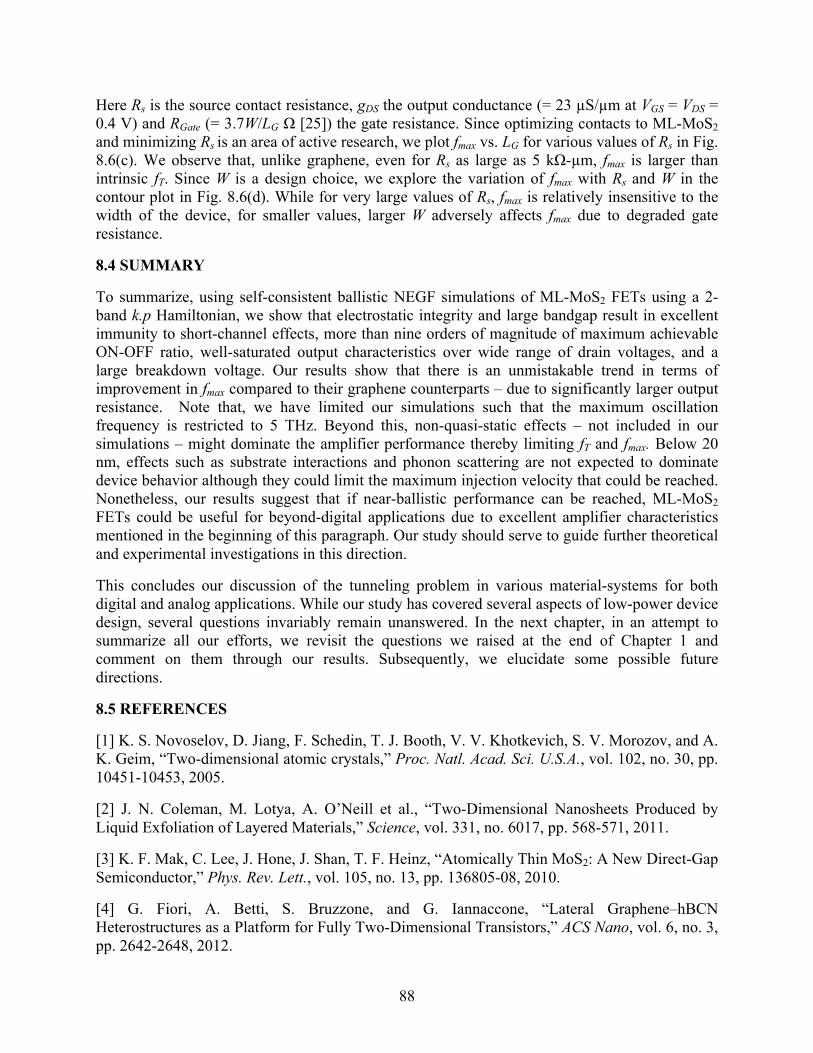
88
Here Rs is the source contact resistance, gDS the output conductance (= 23 µS/µm at VGS = VDS = 0.4 V) and RGate (= 3.7W/LG Ω [25]) the gate resistance. Since optimizing contacts to ML-MoS2 and minimizing Rs is an area of active research, we plot fmax vs. LG for various values of Rs in Fig. 8.6(c). We observe that, unlike graphene, even for Rs as large as 5 kΩ-µm, fmax is larger than intrinsic fT. Since W is a design choice, we explore the variation of fmax with Rs and W in the contour plot in Fig. 8.6(d). While for very large values of Rs, fmax is relatively insensitive to the width of the device, for smaller values, larger W adversely affects fmax due to degraded gate resistance.
8.4 SUMMARY
To summarize, using self-consistent ballistic NEGF simulations of ML-MoS2 FETs using a 2-band k.p Hamiltonian, we show that electrostatic integrity and large bandgap result in excellent immunity to short-channel effects, more than nine orders of magnitude of maximum achievable ON-OFF ratio, well-saturated output characteristics over wide range of drain voltages, and a large breakdown voltage. Our results show that there is an unmistakable trend in terms of improvement in fmax compared to their graphene counterparts – due to significantly larger output resistance. Note that, we have limited our simulations such that the maximum oscillation frequency is restricted to 5 THz. Beyond this, non-quasi-static effects – not included in our simulations – might dominate the amplifier performance thereby limiting fT and fmax. Below 20 nm, effects such as substrate interactions and phonon scattering are not expected to dominate device behavior although they could limit the maximum injection velocity that could be reached. Nonetheless, our results suggest that if near-ballistic performance can be reached, ML-MoS2 FETs could be useful for beyond-digital applications due to excellent amplifier characteristics mentioned in the beginning of this paragraph. Our study should serve to guide further theoretical and experimental investigations in this direction.
This concludes our discussion of the tunneling problem in various material-systems for both digital and analog applications. While our study has covered several aspects of low-power device design, several questions invariably remain unanswered. In the next chapter, in an attempt to summarize all our efforts, we revisit the questions we raised at the end of Chapter 1 and comment on them through our results. Subsequently, we elucidate some possible future directions.
8.5 REFERENCES
[1] K. S. Novoselov, D. Jiang, F. Schedin, T. J. Booth, V. V. Khotkevich, S. V. Morozov, and A. K. Geim, “Two-dimensional atomic crystals,” Proc. Natl. Acad. Sci. U.S.A., vol. 102, no. 30, pp. 10451-10453, 2005.
[2] J. N. Coleman, M. Lotya, A. O’Neill et al., “Two-Dimensional Nanosheets Produced by Liquid Exfoliation of Layered Materials,” Science, vol. 331, no. 6017, pp. 568-571, 2011.
[3] K. F. Mak, C. Lee, J. Hone, J. Shan, T. F. Heinz, “Atomically Thin MoS2: A New Direct-Gap Semiconductor,” Phys. Rev. Lett., vol. 105, no. 13, pp. 136805-08, 2010.
[4] G. Fiori, A. Betti, S. Bruzzone, and G. Iannaccone, “Lateral Graphene–hBCN Heterostructures as a Platform for Fully Two-Dimensional Transistors,” ACS Nano, vol. 6, no. 3, pp. 2642-2648, 2012.
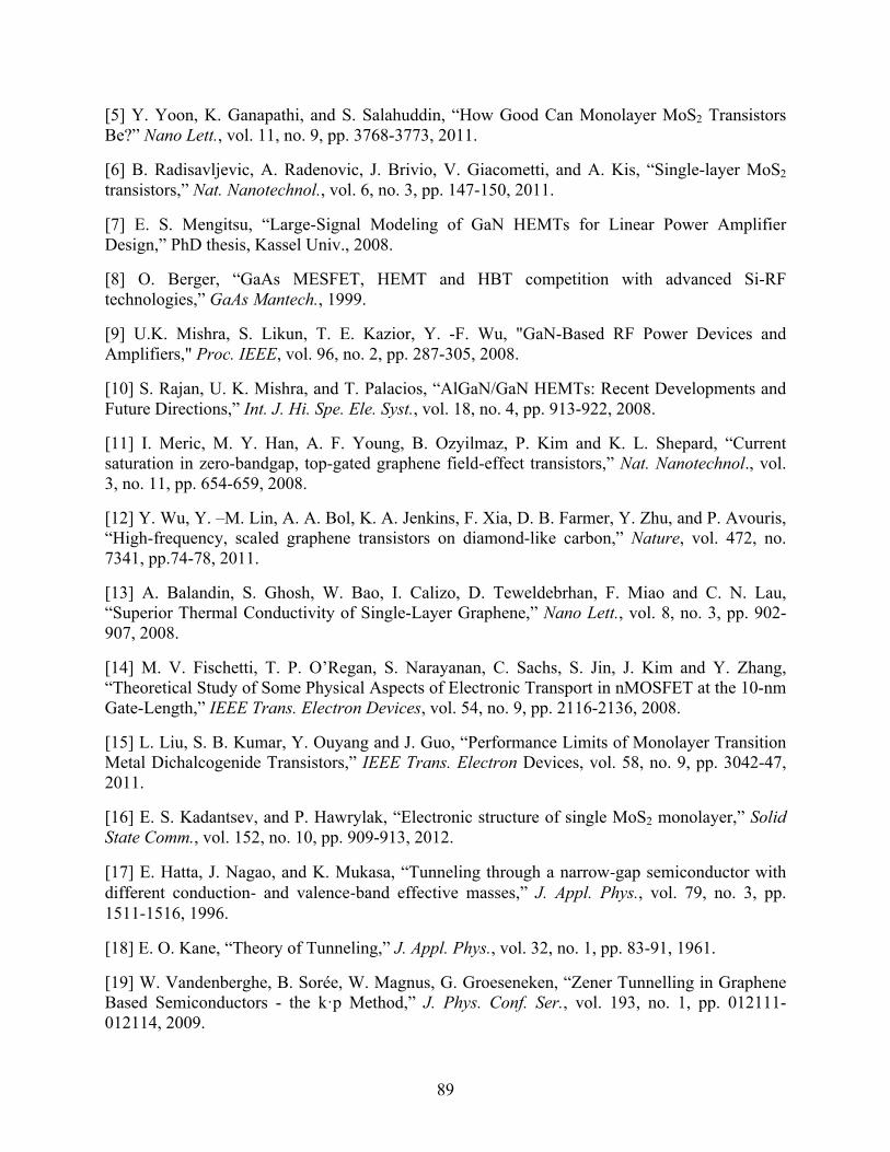
89
[5] Y. Yoon, K. Ganapathi, and S. Salahuddin, “How Good Can Monolayer MoS2 Transistors Be?” Nano Lett., vol. 11, no. 9, pp. 3768-3773, 2011.
[6] B. Radisavljevic, A. Radenovic, J. Brivio, V. Giacometti, and A. Kis, “Single-layer MoS2 transistors,” Nat. Nanotechnol., vol. 6, no. 3, pp. 147-150, 2011.
[7] E. S. Mengitsu, “Large-Signal Modeling of GaN HEMTs for Linear Power Amplifier Design,” PhD thesis, Kassel Univ., 2008.
[8] O. Berger, “GaAs MESFET, HEMT and HBT competition with advanced Si-RF technologies,” GaAs Mantech., 1999.
[9] U.K. Mishra, S. Likun, T. E. Kazior, Y. -F. Wu, "GaN-Based RF Power Devices and Amplifiers," Proc. IEEE, vol. 96, no. 2, pp. 287-305, 2008.
[10] S. Rajan, U. K. Mishra, and T. Palacios, “AlGaN/GaN HEMTs: Recent Developments and Future Directions,” Int. J. Hi. Spe. Ele. Syst., vol. 18, no. 4, pp. 913-922, 2008.
[11] I. Meric, M. Y. Han, A. F. Young, B. Ozyilmaz, P. Kim and K. L. Shepard, “Current saturation in zero-bandgap, top-gated graphene field-effect transistors,” Nat. Nanotechnol., vol. 3, no. 11, pp. 654-659, 2008.
[12] Y. Wu, Y. –M. Lin, A. A. Bol, K. A. Jenkins, F. Xia, D. B. Farmer, Y. Zhu, and P. Avouris, “High-frequency, scaled graphene transistors on diamond-like carbon,” Nature, vol. 472, no. 7341, pp.74-78, 2011.
[13] A. Balandin, S. Ghosh, W. Bao, I. Calizo, D. Teweldebrhan, F. Miao and C. N. Lau, “Superior Thermal Conductivity of Single-Layer Graphene,” Nano Lett., vol. 8, no. 3, pp. 902-907, 2008.
[14] M. V. Fischetti, T. P. O’Regan, S. Narayanan, C. Sachs, S. Jin, J. Kim and Y. Zhang, “Theoretical Study of Some Physical Aspects of Electronic Transport in nMOSFET at the 10-nm Gate-Length,” IEEE Trans. Electron Devices, vol. 54, no. 9, pp. 2116-2136, 2008.
[15] L. Liu, S. B. Kumar, Y. Ouyang and J. Guo, “Performance Limits of Monolayer Transition Metal Dichalcogenide Transistors,” IEEE Trans. Electron Devices, vol. 58, no. 9, pp. 3042-47, 2011.
[16] E. S. Kadantsev, and P. Hawrylak, “Electronic structure of single MoS2 monolayer,” Solid State Comm., vol. 152, no. 10, pp. 909-913, 2012.
[17] E. Hatta, J. Nagao, and K. Mukasa, “Tunneling through a narrow‐gap semiconductor with different conduction‐ and valence‐band effective masses,” J. Appl. Phys., vol. 79, no. 3, pp. 1511-1516, 1996.
[18] E. O. Kane, “Theory of Tunneling,” J. Appl. Phys., vol. 32, no. 1, pp. 83-91, 1961.
[19] W. Vandenberghe, B. Sorée, W. Magnus, G. Groeseneken, “Zener Tunnelling in Graphene Based Semiconductors - the k·p Method,” J. Phys. Conf. Ser., vol. 193, no. 1, pp. 012111-012114, 2009.
90
[20] S. Lebègue and O. Eriksson, “Electronic structure of two-dimensional crystals from ab initio theory,” Phys. Rev. B, vol. 79, no. 11, pp.115409-12, 2009.
[21] Simulation results at even smaller values of VGS could not be obtained due to insufficient bandwidth of the Hamiltonian, which is a result of using small number of bands.
[22] K. Ganapathi, Y. Yoon, M. Lundstrom and S. Salahuddin, “Ballistic I – V Characteristics of Short-Channel Graphene Field-Effect Transistors: Analysis and Optimization for Analog and RF Applications,” IEEE Trans. Electron Devices, vol. 60, no. 3, pp. 958-964, 2013.
[23] A similar calculation of n (through integration of DOS) also shows a square-law behavior.
[24] It remains to be investigated if a richer and more detailed description of the Hamiltonian e.g., ab-initio-based bandstructure possessing similar symmetries, retains the square-law properties discussed herein.
[25] J. S. Shin, H. Bae, E. Hong, J. Jang, D. Yun, J. Lee, D. H. Kim, and D. M. Kim, “Modeling and extraction technique for parasitic resistances in MOSFETs Combining DC I–V and low frequency C–V measurement,” Solid State Electronics, vol. 72, no. 6, pp. 78-81, 2012.

91
CHAPTER 9
CONCLUSIONS AND FUTURE WORK In this chapter, we summarize our findings on exploiting tunneling as a means to realize next-generation of low-power devices. Our discussion would be guided by the questions we raised in Section 1.5. After having consolidated our learning, we outline some directions for future work, from the viewpoint of simulation techniques as well as that of device-design problems. We also identify some experiments for benchmarking them and also some potential roadblocks.
9.1 CONSOLIDATING WHAT WE HAVE LEARNED SO FAR…
Having argued strongly in favor of the need for fully quantum-mechanical solution to the electronic transport problem given the length-scales and physical phenomenon of our interest i.e., tunneling, we set out to build a generic, massively parallel, NEGF-based quantum transport simulator. In Chapter 2, we laid down the formalism, the algorithms used to accelerate the calculations, and the capabilities of BQTS in terms of both device geometries and electronic structures. We also demonstrated the scalability that could be achieved with BQTS (up to roughly 8000 processors) which enabled use to look at realistic-size devices with an elaborate enough bandstructure description. The generality of the simulator can be inferred from Fig. 9.1, which provides an overview of some of the physical systems we have examined using BQTS [1]-[7].
9.1.1 COMPARISON BETWEEN SEMI-CLASSICAL AND QUANTUM FORMALISMS
Chapter 4 helped us address the issue of differences between semi-classical and quantum formalisms in the context of tunneling. In particular, in addition to the absence of coherence and
Figure 9.1: Overview of some of the physical systems investigated using BQTS.
!!"#$%&"'()*+,"
"!"#$%&"-(+.,/"
""#$%&"0*12$"
#"3(45"
61/,!!
61/,!!
7824,"
7824,"
#$9:;<619:=>%&?#$%&"
@A,/,*(?A(B(C"
Mono- and few-layer MoS2
Graphene FETs
n-type p-type
InAs Tunnel Diode
Substrate
S
Gate
Oxide
Graphene
D
III-V Homo- & Hetero-junction TFETs

92
interference effects in the former, we noticed that the evaluation of action integral – along the imaginary wavevector – in a WKB-like approach only matches the NEGF result qualitatively in terms of variation of transmission coefficient with energy (in the band overlap region), in spite of using the same electrostatic potential profile as the latter. We also noticed that quantitative matching of WKB current with NEGF values is harder to achieve at all doping concentrations and bias voltages with a single multiplicative prefactor, which signals a more subtle difference between the two. Our results showed that the simple Kane’s model, the variants of which have been used extensively in the past in device simulation packages, fails to capture the non-uniformity of field for most electric fields of our interest.
9.1.2 CONFINEMENT EFFECTS
We noted, in Chapter 2, that both k.p and tight-binding methods allow quantitative incorporation of finite-size effects in the Hamiltonian description. Given that most modern-day devices have some geometric confinement, we implicitly account for such effects, otherwise taken into consideration in an ad hoc manner in TCAD packages.
One example of manifestation of confinement was in Chapter 5, where our simulations showed that for body thicknesses smaller than a critical value, vertical tunneling would be absent due to larger bandgap and a fully depleted body. Another instance where confinement-effects surfaced is in the capacitance characteristics of monolayer MoS2 FETs in Chapter 3, where we concluded that one of the reasons for saturation of quantum capacitance (CQ) to a value much smaller than the expected, ideal 2-D CQ was due to confinement along the transport direction. This was also confirmed by density-of-states plot that resembled that of a 1-D system. A third occasion where the phenomenon played a prominent role in determining device behavior was in the observation of negative transconductance in hetero-VTFETs, discussed in Chapter 6. The occurrence of negative differential resistance in the output characteristics of p-type doped graphene FETs in Chapter 7 is also due to confinement.
9.1.3 LEVEL BROADENING EFFECTS
While ballistic simulations do not contain the effect of broadening of states due to scattering, they do have the broadening from the contacts included. The qualitative difference with and without incorporation of this is significant in TFETs. Drift-diffusion-based simulators that do not account for broadening of channel states due to coupling to reservoirs wrongly estimate the OFF-state leakage and also the subthreshold swing (SS). An illustration of this can be seen in Chapter 5 where our NEGF simulations show that, contrary to expectations, short-channel InAs TFETs do not exhibit a swing less than 60 mV/decade in spite of excellent electrostatics. On the other hand, studies using an explicit band-to-band tunneling generation-rate, depending on presence or absence of band overlap, have been overly optimistic in their SS estimates [8].
9.1.4 INSIGHTS IN TUNNEL-FET DESIGN
In terms of TFET-design insights, two ideas are worthy of mention here. The first observation, is that homojunction vertical TFETs, in sub-20 nm regime, perform only marginally better than their lateral counterparts due to parasitic lateral TFET underneath the pocket therein, that sets the lower bound on the minimum achievable leakage current. The second observation is on the effectiveness of mole fraction of a ternary III-V semiconductor as a knob to tune the switching

93
steepness in case of hetero-VTFETs. As was seen in Chapter 6, band-offsets in a staggered-band configuration can shift the turn-on voltage such that the onset of tunneling in the pocket region and the region underneath it occurs in the same bias range. This shift in turn-on voltage also results in vertical tunneling component becoming a factor in increasing the abruptness of characteristics. More generally, hetero-VTFET provides conceptual pathways to think about steep subthreshold devices with high ON current, wherein the key is to (a) create a huge non-equilibrium distribution of carriers in the source of an FET in OFF state, and (b) ensure that this distribution remains more or less intact during FET barrier-lowering.
9.1.5 TUNNELING INSIGHTS IN MOSFET-DESIGN
One of the questions we set out to answer was if understanding tunneling in TFETs helps us design better MOSFETs made of layered materials. We showed that the answer to this question is in the positive through our proposal to delay the onset of tunneling in graphene FETs (GFETs) by doping the drain underlap region p-type, and hence to increase their output resistance and intrinsic gain. We pointed out that the scaling trends in intrinsic cutoff frequency (fT) of GFETs could deviate from the expected behavior due to tunneling and also provided plausible mechanisms that might result in experimentally observed trends. Our results also demonstrated the trade-off between electrostatic control and fT therein due to pronounced tunneling at ultra-thin oxide thicknesses (Chapter 7).
Another insight we gained, in Chapter 8, was that a large bandgap – as in case of monolayer MoS2 – that inhibits band-to-band tunneling and therefore leads to a large output resistance could translate to a large maximum oscillation frequency (fmax) although fT might be smaller than in a narrow bandgap semiconductor owing to its heavier effective mass (in most semiconductors, there exists a direct correlation between effective mass and bandgap).
9.2 FUTURE DIRECTIONS
9.2.1 DISSIPATIVE TRANSPORT
Although in all our studies we ignored the effects of carrier scattering – either with phonons, impurities, or other carriers – it is very natural to expect some amount of it in most conventional semiconductors at room temperature. For modern-day devices that are largely intentionally undoped, the primary source of scattering comes from phonons. While in most cases, acoustic and optical phonons play a major role in determining the extent of scattering carriers undergo, in polar semiconductors (like III-Vs) polar optical phonons too play a dominant role.
More specifically, in addition to the expected degradation in ON state current due to scattering, there could be implications also on the OFF-state characteristics. For example, in graphene-nanoribbon based TFETs, phonon scattering has been shown to give rise to sub-bands in the bandgap region (due to level broadening), thereby lowering the effective bandgap, and hence setting the floor on minimum achievable SS and OFF current [9]. Given this, it becomes very important to incorporate the effect in our simulations to determine its extent on switching characteristics.
The inclusion of the effect of scattering, through a self-energy term, in the NEGF formalism is, conceptually, relatively straightforward [10], [11]. However, from practicality standpoint, there exist two major challenges. Firstly, the problem becomes computationally extremely unwieldy as

94
(a) the inherent parallelism present in the ballistic transport equations is broken due to coupling between Green’s function variables of different energies and momenta; and (b) as a result, the calculation of Σs introduces another self-consistency loop within the transport equations, in addition to the self-consistency with Pöisson’s equation. Secondly, accurate theoretical determination of the electron-phonon interaction coefficients is difficult – the results from density functional theory based calculations fare poorly in reproducing experimental parameters such as mobility, mean-free-path etc. Hence these matrix elements have been used, in the past, as fitting parameters to match experimental results.
Due to the computational burden, solving dissipative NEGF equations has so far been limited to relatively smaller systems and/or with several simplifying approximations. However, in order to solve phonon scattering problems at the length-scales of modern-day devices, several modifications to the underlying algorithms are necessary: (i) a significant amount of speedup could be expected by solving NEGF equations over a non-uniform, adaptive mesh of energy and momentum variables; (ii) a greater amount of parallelism could be achieved by computing the linear algebra operations over multiple processors. In addition to these, a fast and scalable method, along the lines of recursive Green’s function, would be required. In order to figure out the appropriate range of parameters for the deformation potentials, benchmarking with experiments would be necessary. Specifically, for common semiconductors there exists wealth of two-terminal tunnel diode characteristics – often together with temperature dependence – that could be used [12], [13]. The peak-to-valley ratio in the forward-biased, negative differential resistance region – a strong function of phonon scattering – could be used as a signature. However, in most practical cases, there would be some contribution to tunneling from localized trap-states.
One of the interesting directions would be to revisit the hetero-VTFET with a model that includes phonon scattering and examine if (a) the steepness of the turn-on is still preserved and (b) the negative transconductance is washed out due to scattering. In Chapter 6, we argued that the steepness is likely to be preserved due to the fact that turn-on is not very sensitive to broadening of states near the valence band edge of source end – unlike in lateral TFET – and scattering would merely cause a shift in switching voltage. We could argue, based on our understanding of negative transconductance, that it would indeed be smeared out as the phenomenon is contingent on the alignment of confined states that get broadened due to scattering.
9.2.2 DENSITY FUNCTIONAL THEORY
Density functional theory (DFT) is a powerful ab initio technique for exploration of material properties. It provides a first-principles approach to calculate the electronic structure of various material-systems. While so far we have mainly worked with orthogonal bases description of Hamiltonian, extension of the simulator to incorporate non-orthogonal bases would facilitate straightforward use of DFT-based bandstructure in transport calculations in a plethora of scenarios without having to parameterize the dispersion relations in an orthogonal basis.
Another instance of interaction between transport models and DFT could be in determination of electron-phonon interaction coefficients. It has been observed in several experiments that layered materials in general, and graphene in particular suffer severe degradation of their superior intrinsic material properties due to interactions with substrate phonons. DFT provides a

95
quantitative way of describing such effects. One more interesting future direction could be in the use of DFT in conjunction with a dissipative transport model to engineer the phonon modes in the system. Depending on the application of interest, phonon modes could be tuned through electrical and/or mechanical boundary conditions so as to optimize electron-phonon interactions.
9.2.3 INCORPORATING GATE TUNNELING AND STRAIN
While the problem of gate tunneling is mitigated to a large extent through the use of high-κ dielectric that results in small electrical thickness while maintaining large physical thickness, in case of some materials, compatible high-κ may not be available (and hence using a thin layer SiO2 along with high-κ becomes inevitable) or aggressive thickness scaling might be essential to gain performance boost. Such situations call for an accurate modeling of gate tunneling current – something we ignored in all our previous simulations. However, from a formalism viewpoint, incorporating gate tunneling simply involves addition of self-energy for the gate, which has been discussed previously in the literature [14], [15].
Another physical effect that needs incorporation from a technological relevance standpoint is strain. Stress engineering is being used in modern CMOS processes to enhance mobility for quite a few years. Also, in heterostructures, due to lattice mismatch, thin films get stressed and hence experience strain. The effect of strain is to modify the bandstructure and hence the carrier effective mass. The k.p and tight-binding methods provide a straightforward approach to modify the model parameters depending on the magnitude of strain [16], [17]. With two effects included, BQTS could become a fairly complete simulator for investigating transport phenomenon in most of today’s short-channel CMOS devices.
9.3 EPILOGUE
We have built the Berkeley Quantum Transport Simulator – a massively parallel, generic, NEGF-based quantum transport simulator and have investigated several physical systems in the context of low-power device-design. We have also established some connections with and provided interpretations to experimental data. All this while, our focus has been on understanding and engineering tunneling in different materials and geometries for both digital and analog applications. We believe that band-to-band tunneling is one of the most promising charge-based physical phenomena that has true potential of being a next-generation technology, in spite of challenges on the experimental front. Furthermore, in our opinion, BQTS could serve as a very good starting point for incorporating descriptions of richer, complex and elaborate physical mechanisms that govern the behavior of devices of the future. This, in turn, could take us one step closer to the holy grail of predictive modeling of electronic devices.
9.4 REFERENCES
[1] K. Ganapathi, Y. Yoon and S. Salahuddin, “Analysis of InAs vertical and lateral band-to-band tunneling transistors: Leveraging vertical tunneling for improved performance,” Appl. Phys. Lett., vol. 97, no. 3, pp. 033504-033506, 2010.
[2] K. Ganapathi, and S. Salahuddin, “Heterojunction Vertical Band-to-Band Tunneling Transistors for Steep Subthreshold Swing and High on Current,” IEEE Electron Device Lett., vol. 32, no. 5, pp. 689-691, 2011.
96
[3] Y. Yoon, K. Ganapathi, and S. Salahuddin, “How Good Can Monolayer MoS2 Transistors Be?” Nano Lett., vol. 11, no. 9, pp. 3768-3773, 2011.
[4] K. Ganapathi, and S. Salahuddin, “Zener tunneling: Congruence between semi-classical and quantum ballistic formalisms,” J. Appl. Phys., vol. 111, no. 12, pp. 124506-124509, 2012.
[5] K. Ganapathi, Y. Yoon and S. Salahuddin, “Intrinsic Cut-off Frequency in Scaled Graphene Transistors,” arXiv: 1110.6211v1, 2011.
[6] H. Ko, K. Takei, R. Kapadia et al., “Ultrathin compound semiconductor on insulator layers for high performance nanoscale transistors”, Nature, vol. 468, no. 7321, pp. 286-289, 2010.
[7] K. Ganapathi, Y. Yoon, M. S. Lundstrom and S. Salahuddin, “Ballistic I-V Characteristics of Short-Channel Graphene Field-Effect Transistors: Analysis and Optimization for Analog and RF Applications,” IEEE Trans. Electron Devices, vol. 60, no. 3, pp. 958-964, 2013.
[8] A. Bowonder, P. Patel, K. Jeon, J. Oh, P. Majhi, H. -H. Tseng and C. Hu, “Low-voltage green transistor using ultra shallow junction and hetero-tunneling”, in International Workshop on Junction Technology, Shanghai, 2008, pp. 93-96.
[9] Y. Yoon, and S. Salahuddin, “Dissipative transport in rough edge graphene nanoribbon tunnel transistors,” Appl. Phys. Lett., vol. 101, no. 26, pp. 263501-263504, 2012.
[10] D. E. Nikonov, H. Pal, G. Bourianoff, “Scattering in NEGF: Made simple,” https://nanohub.org/resources/7772, 2009.
[11] S. Datta, “Quantum transport: atom to transistor,” Cambridge University Press, 2005.
[12] G. Zhou, Y. Lu, R. Li, et al., “Vertical InGaAs/InP Tunnel FETs With Tunneling Normal to the Gate,” IEEE Electron Device Lett., vol.32, no.11, pp.1516-1518, 2011.
[13] W. -Y. Loh, K. Jeon, C. Y. Kang, J. Oh, T. -J. King Liu, H. -H. Tseng, W. Xiong, P. Majhi, R. Jammy, C. Hu, “Highly scaled (Lg ∼ 56 nm) gate-last Si tunnel field-effect transistors with ION > 100 µA/µm,” Solid State Electron., vol. 65-66, pp. 22-27, 2011.
[14] M. Luisier, and A. Schenk, “Two-Dimensional Tunneling Effects on the Leakage Current of MOSFETs With Single Dielectric and High-κ Gate Stacks,” IEEE Trans. Electron Devices, vol. 55, no. 6, pp. 1494-1501, 2008.
[15] A. Svizhenko, M. P. Anantram, T. R. Govindan, R. Biegel, and R. Venugopal, “Two-dimensional quantum mechanical modeling of nanotransistors,” J. Appl. Phys., vol. 91, no. 4, pp. 2343-2354, 2002.
[16] T. B. Boykin, M. Luisier, M. S. –Jelodar, and G. Klimeck, “Strain-induced, off-diagonal, same-atom parameters in empirical tight-binding theory suitable for [110] uniaxial strain applied to a silicon parametrization,” Phys. Rev. B, vol. 81, no. 12, pp. 125202-125210, 2010.
[17] D. Gershoni, C. H. Henry and G.A. Baraff, “Calculating the optical properties of Multidimensional Heterostructures: Application to the Modeling of Quaternary Quantum Well Lasers,” IEEE J. Quantum Elect., vol. 29, no. 9, pp. 2433-2450, 2008.