Resonant Tunneling Device - Rowan...
32
Resonant Tunneling Device Kalpesh Raval
Transcript of Resonant Tunneling Device - Rowan...
Resonant Tunneling Device
Kalpesh Raval

Outline• Diode basics• History of Tunnel diode• RTD Characteristics & Operation• Tunneling Requirements• Various Heterostructures• Fabrication Technique• Challenges• Application & Integration• Conclusion
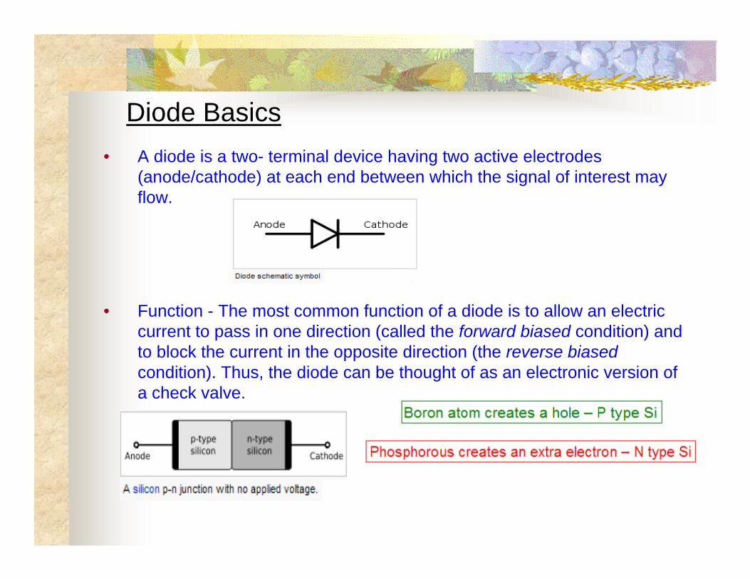
Diode Basics• A diode is a two- terminal device having two active electrodes
(anode/cathode) at each end between which the signal of interest may flow.
• Function - The most common function of a diode is to allow an electric current to pass in one direction (called the forward biased condition) and to block the current in the opposite direction (the reverse biasedcondition). Thus, the diode can be thought of as an electronic version of a check valve.

• Forward Bias - Forward-bias occurs when the P-type semiconductor material is connected to the positive terminal of a battery and the N-typesemiconductor material is connected to the negative terminal. This makes the P-N junction conduct.
• Reverse Bias - If a diode is reverse biased, the voltage at the cathode is higher than that at the anode. Therefore, no current will flow until the diode breaks down. Connecting the P-type region to the negative terminal of the battery and the N-type region to the positive terminal, produces the reverse-bias effect.
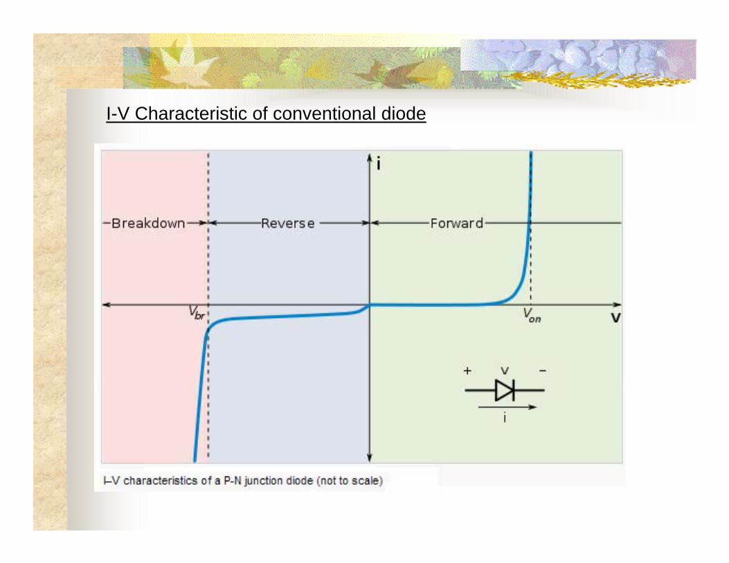
I-V Characteristic of conventional diode

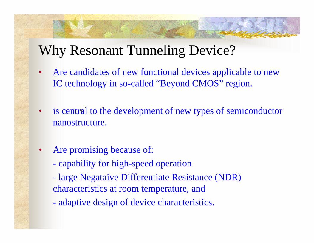
Why Resonant Tunneling Device?• Are candidates of new functional devices applicable to new
IC technology in so-called “Beyond CMOS” region.
• is central to the development of new types of semiconductor nanostructure.
• Are promising because of:- capability for high-speed operation- large Negataive Differentiate Resistance (NDR) characteristics at room temperature, and - adaptive design of device characteristics.

Why RTD?• Lower sub-threshold swing can allow for lower
operating voltages to be used
• Negative differential resistance (NDR) properties can be exploited to create simpler designs for bi-stable circuits, differential comparators, oscillators, etc.
• Leads to chips that consume less power (few mAmps to a few tenths of a volt)

History of Tunnel diode
• Invented in August 1957 by Leo Esaki while working at Tokyo Tsushin Kogyo (now known as SONY). It was a 1st quantum electron device.
• In 1973, he received the Nobel Prize in Physics for discovering the electron tunneling effect used in these diodes.
• A tunnel diode (Esaki diode) can operate at (.3 – 300 GHz) & terahertz (x10^12 Hz ) at room temperature by using quantum mechanical effects.
• RTDs are formed as a single quantum well structure that is surrounded by thin layer barriers known as a double-barrier structure.
• Initially manufactured by SONY in 1958 followed by General Electric and other companies from 1960.
• RTDs are being manufactured in low volume today.
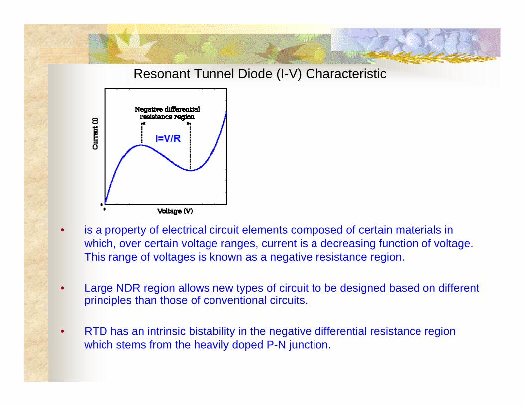
Resonant Tunnel Diode (I-V) Characteristic
• is a property of electrical circuit elements composed of certain materials in which, over certain voltage ranges, current is a decreasing function of voltage. This range of voltages is known as a negative resistance region.
• Large NDR region allows new types of circuit to be designed based on different principles than those of conventional circuits.
• RTD has an intrinsic bistability in the negative differential resistance region which stems from the heavily doped P-N junction.
Operation
• Heavily doped P-N junction results in extremely narrow depletion zone (one-millionth of an inch).
• 1000 impurity atoms for ten-million semiconductor atoms vs. 1 impurity atom used in a normal diode.
• Leads to overlap of conduction and valence bands.

Operation

Tunnel Diode
• Forward Bias Operation
-Tunnel diodes have a heavily doped p-n junction approximately 10 nm (100 A°) wide which results in overlap between energy bands.
- As voltage begins to increase, electrons at first tunnel through the very narrow p-n junction barrier causing current to increase.
- As voltage increases further these states become more misaligned and the current drops this is called negative resistance, because current decreases with increasing voltage.
- As voltage increases yet further, the diode begins to operate as a normal diode, where electrons travel by conduction across the p-n junction, and no longer by tunneling through the p-n junction barrier.

Resonant Tunneling
• Tunneling is a quantum mechanical phenomenon with no analogy in classical physics.
• Occurs when an electron passes through a potential barrier without having enough energy to do so.
• Resonant tunneling can be described by the transmission and reflection processes of coherent electron waves through the double barrier structure.
• Can be seen as leaking of the amplitude through the potential step.
http://en.wikipedia.org/wiki/File:EffetTunnel.gif

Tunneling
• Even though the transmission coefficient or the tunneling probability of an incident particle through the barrier is always less than one and decreases with increasing barrier height and width,two barriers in a row can be completely transparent for certain energies of the incident particle. This phenomenon is called resonant tunneling.

Tunneling Requirements
• Need good (high quality) heterostructures• Quantum well layers• Tunnel layers with high energy-barriers• Requires junction to be abrupt• Above, currently difficult on Si substrate

Heterostructures• Heterostructures are structures with two or more interfaces at the
boundaries between the regions of different materials.
• Compound semiconductors from Group (III – V) are widely used to fabricate heterostructures. A double-barrier structure can be grown by molecular beam heteroepitaxy (MBE).
• Common compounds used are GaAs (gallium arsenide) and AlAs (aluminum arsenide)
• Band offsets at the boundary of heterojunction can depend on the quality of the interface, conditions of growth etc.
• Types I, II and broken-gap lineup heterojunctions

• Type I – The lowest conduction-band states occur in the same part of the structure as the highest valence-band states. (GaAs/AlxGa1-xAs, is type I)
• Type II – The lowest conduction-band minimum occurs on one side and the highest valence-band maximum on the other with an energy separation between the two is less than the lower of the two bulk bandgaps.(AlAs/AlxGa1-xAs and some Si/SixGe1-x structures)
• Broken-gap lineup – The bottom of the conduction band on one side drops below the top of the valence band on the other. (InAs/GaSb gap of 150meV)

Molecular Beam Epitaxy Lab
The most important aspect of MBE is the slow deposition rate, typically less than 1000 nm (1 micron) per hour, which allows the films to grow epitaxially.

Conduction band profiles of a double barrier RTD

RTD Challenges
• Scalability to below certain dimensions result in undesirable surface leakage current.
• Since the peak current through an RTD depends exponentially on the barrier thickness, it is difficult to get device operation unless the gate also controls the peak current.
• Integration of a transistor with a pair of RTDs introduces delays to the fast bistable switching times so, the operational speed of the integrated device can be slower than the intrinsic speeds of the RTDs themselves.
• The precise control of the layer thickness and properties of RTDs may require use of commercial molecular beam epitaxy to achieve the required control.
• A limited ION/IOFF ratio of 10 compare to the ratio of 105 required by CMOS digital circuit designers.
• Fabrication of silicon or silicon-germanium tunnel diodes with high peak-to-valley current ratios.
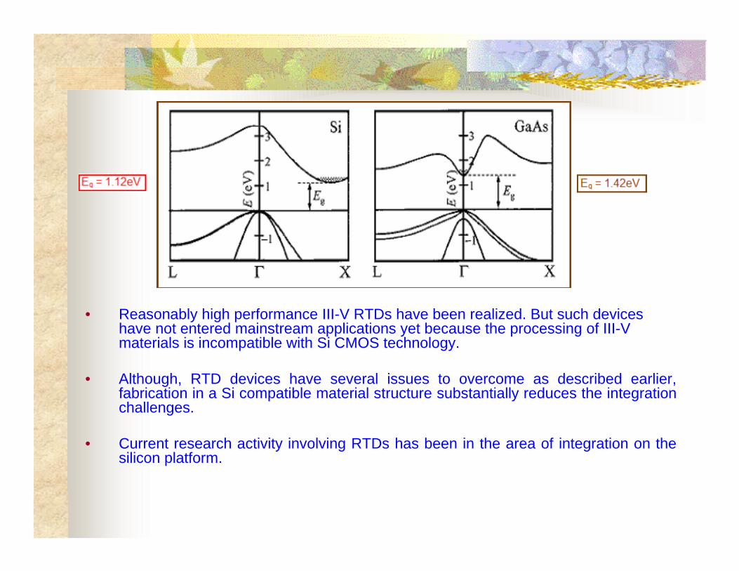
• Reasonably high performance III-V RTDs have been realized. But such devices have not entered mainstream applications yet because the processing of III-V materials is incompatible with Si CMOS technology.
• Although, RTD devices have several issues to overcome as described earlier, fabrication in a Si compatible material structure substantially reduces the integration challenges.
• Current research activity involving RTDs has been in the area of integration on the silicon platform.

RTD on Si Substrates using Fluoride Alloy Heterostructures
• RTDs composed of CaF2-barrier/CdF2-well/ CaF2-barrierheterostructures are expected to be co-integrated with Si-Large Scale Integration (LSI).
• High speed LSI and low power consumption can be constructed in Si-integrated circuits.
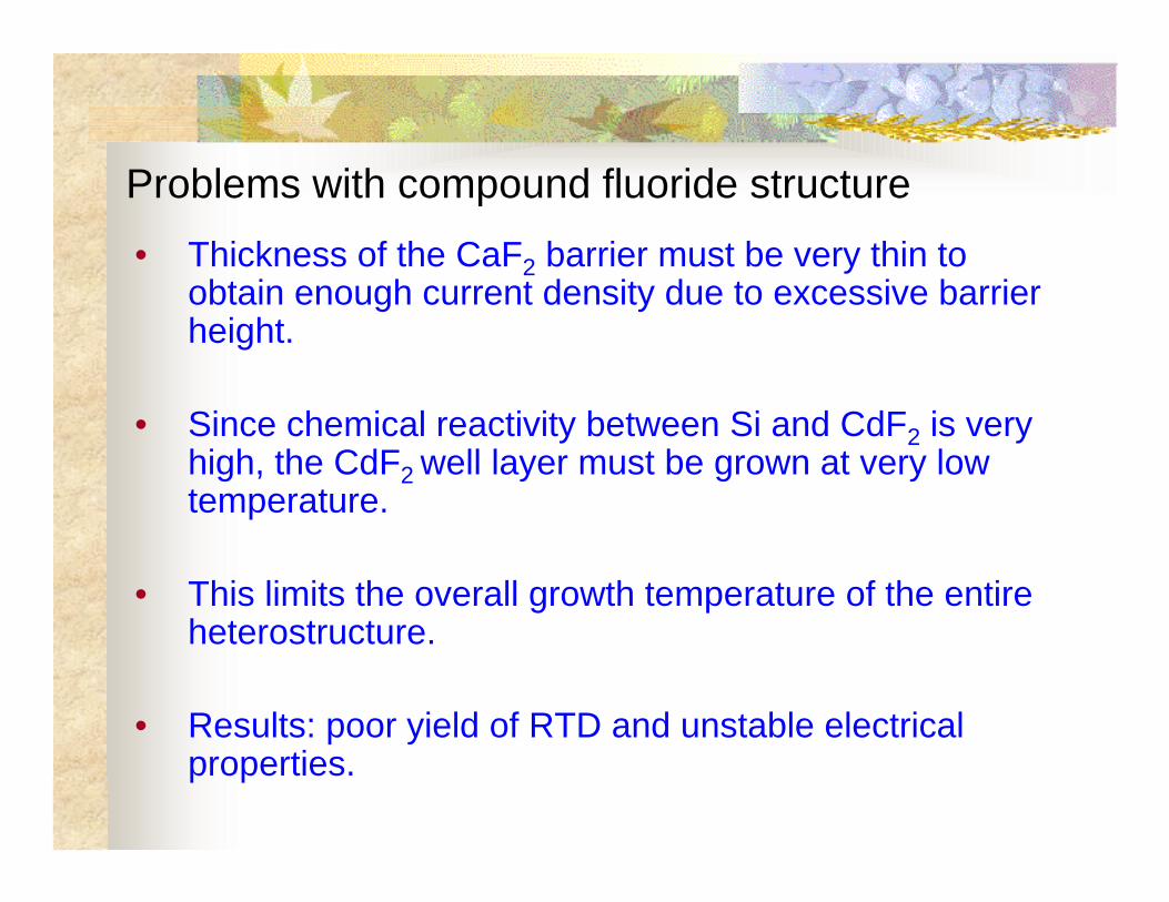
Problems with compound fluoride structure• Thickness of the CaF2 barrier must be very thin to
obtain enough current density due to excessive barrier height.
• Since chemical reactivity between Si and CdF2 is very high, the CdF2 well layer must be grown at very low temperature.
• This limits the overall growth temperature of the entire heterostructure.
• Results: poor yield of RTD and unstable electrical properties.
Solution
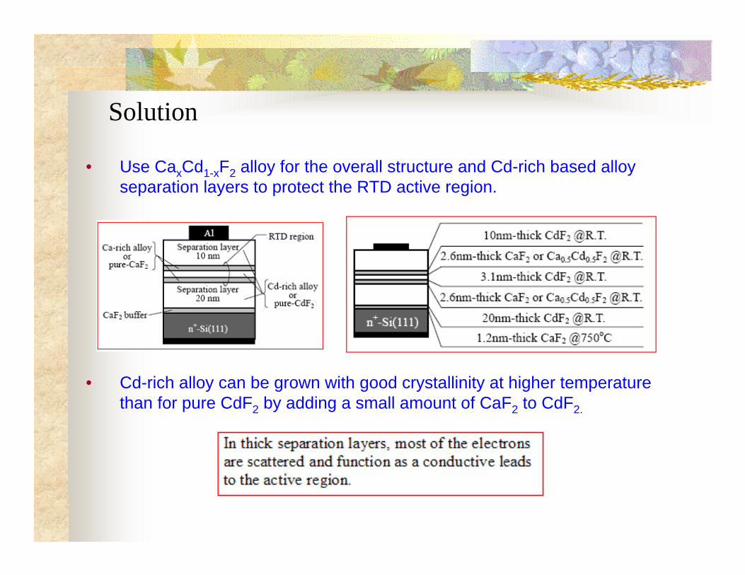
• Use CaxCd1-xF2 alloy for the overall structure and Cd-rich based alloy separation layers to protect the RTD active region.
• Cd-rich alloy can be grown with good crystallinity at higher temperature than for pure CdF2 by adding a small amount of CaF2 to CdF2.

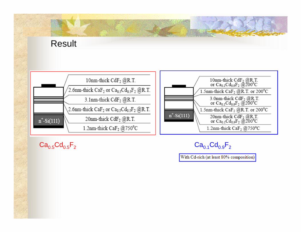
Solution• The alloy Ca0.5Cd0.5F2 showed the lower barrier height instead of CaF2 and
high PVCR.
• Similarly, RTDs using the Cd-rich alloy for the well exhibited even larger peak to valley current ratio at room temperature b/c of good crystallinity.
Result
Ca0.5Cd0.5F2 Ca0.1Cd0.9F2

Applications
• OptoElectronic Integrated Circuits (OEICS) based on Group III-V RTDs
• can be used as oscillators, high frequency amplifiers, frequency converters and photodetectors.
• MOBILE circuits used in ultra high-speed analog to digital converters (80 Gb/s). MOBILE type structures can be applied to multi-valued threshold circuits and multi-threshold gates in general.
• Resonant-tunneling transistors - a negative transconductance that is used in logic XOR gate with only one transistor.
• Recent works also explore spin-polarized resonant tunneling, which can be useful for application in spintronic devices.
Integration of RTDs
• A pair of RTDs can be integrated with CMOS gate to achieve bi-stable operation. If connected in series with opposing polarities, results in MOBILE configuration.
• Trials of co-integration of the fluoride RTDs with Si-MOSFET have been reported. However, stability of electrical properties of the RTDs is insufficient (current drift) to realize circuit operations well at the moment. The origin is presumably charging effects of carrier traps in heterostructures.
• Further investigation to improve crystalline quality of the fluoride heterostructures is necessary to achieve reliable circuit operation of this device.
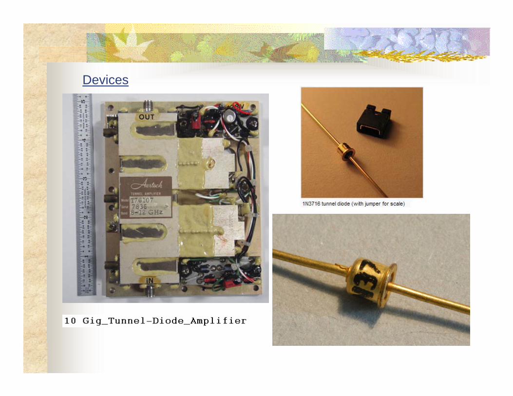
Devices

Conclusion
• Tunnel diodes are expected to add another node in the road
• Three-terminal tunnel devices could add several nodes at the end of CMOS-scaling
• Challenges are more practical than theoretical• Uniformity of the tunneling barrier needs to
be improved

References
• David Bohm, Quantum Theory, Prentice-Hall, New York, 1951.
• Baym Gordon, Lectures on Quantum Mechanics, Addison-Wesley Company, Canada, 1969.
• H. Mizuta and T. Tanoue. “The Physics and applications of Resonant TunnellingDiodes.” Cambridge University Press, Cambridge 1995.
• Koichi Maezawa. “Resonant Tunneling Diodes and Their Application to High-Speed Circuits.” CSIC 2005 Digest, IEEE.
• http://en.wikipedia.org/wiki/Resonant_tunnelling_diode
• http://www.imec.be/esscirc/essderc-esscirc-2003/papers/all/182.pdf