
Tunable Optoelectronic Devices - University of California, Berkeley
236
Tunable Optoelectronic Devices by Carlos Fernando Rondina Mateus Engineer (Aeronautics Institute of Technology) 1996 Grad (Aeronautics Institute of Technology) 1997 A dissertation submitted in partial satisfaction of the requirements for the degree of Doctor of Philosophy in Engineering – Electrical Engineering and Computer Sciences in the GRADUATE DIVISION of the UNIVERSITY of CALIFORNIA at BERKELEY Committee in charge: Prof. Constance J. Chang-Hasnain, Chair Prof. Nathan Cheung Prof. Yuri Suzuki Spring 2004
Transcript of Tunable Optoelectronic Devices - University of California, Berkeley

Tunable Optoelectronic Devices
by
Carlos Fernando Rondina Mateus
Engineer (Aeronautics Institute of Technology) 1996 Grad (Aeronautics Institute of Technology) 1997
A dissertation submitted in partial satisfaction of the requirements for the degree of
Doctor of Philosophy
in
Engineering – Electrical Engineering and Computer Sciences
in the
GRADUATE DIVISION of the
UNIVERSITY of CALIFORNIA at BERKELEY Committee in charge:
Prof. Constance J. Chang-Hasnain, Chair Prof. Nathan Cheung Prof. Yuri Suzuki
Spring 2004


Tunable Optoelectronic Devices
Copyright Spring 2004
by
Carlos Fernando Rondina Mateus

1
Abstract
Tunable Optoelectronic Devices by
Carlos Fernando Rondina Mateus
Doctor of Philosophy in Engineering – Electrical Engineering and Computer Sciences
University of California, Berkeley
Professor Constance J. Chang-Hasnain, Chair
Tunable devices, specifically filter, detector and laser, are key components for a
variety of applications such as communications, spectroscopy, biosensing, inter and intra-
chip connection, infrared (IR) imaging, and biometrics. Monolithically tuned devices are
even more attractive because of compactness, robustness, easiness of integration, and low
price inherent to semiconductor batch fabrication and testing.
This dissertation discusses design, fabrication and applications of monolithically
tuned optoelectronic devices. The devices have vertical optical cavity with respect to the
substrate, which uses micromaching techniques to provide the largest monolithic tuning
range among all options.
Design is described in separate for optical cavity and mechanical beams. A novel
grating mirror, with both high bandwidth and reflectivity, is theoretically and
experimentally demonstrated as an alternative to the conventional distributed Bragg
reflectors. General design rules and scaling laws with wavelength are presented in a
flowchart as function of system requirements such as tuning range, central wavelength,
tuning voltage, tuning speed and resolution. By following the various steps, all

2

i
To my wife, Anna Paula,
who always gave support and strength for me to pursue my dreams.

ii
Table of Contents
CHAPTER 1 INTRODUCTION ............................................................................................................1 1.1 Introduction......................................................................................................... 1 1.2 Applications of tunable devices .......................................................................... 4
1.2.a Communications – Wavelength Division Multiplexing (WDM) ............... 4 1.2.b Spectroscopy............................................................................................... 8 1.2.c Biosensing................................................................................................. 10 1.2.d Infrared (IR) imaging................................................................................ 11 1.2.e Biometrics ................................................................................................. 13
1.3 Overview of the dissertation ............................................................................. 14 CHAPTER 2 DESIGN...........................................................................................................................17
2.1 Introduction....................................................................................................... 17 2.2 Optical Cavity ................................................................................................... 18
2.2.a Distributed Bragg Reflector (DBR) .......................................................... 23 2.2.a.1 Transmission Matrix ................................................................................. 24
2.2.b Sub-Wavelength Grating (SWG).............................................................. 27 2.2.b.1 Rigorous Coupled Wave Analysis (RCWA) ............................................ 34
2.2.c Comparison between DBR and SWG....................................................... 35 2.3 Mechanical Structure ........................................................................................ 38 2.4 General Design Rules ....................................................................................... 44
2.4.a Torsional Design....................................................................................... 51 2.5 Summary ........................................................................................................... 54
CHAPTER 3 FABRICATION..............................................................................................................55 3.1 Introduction....................................................................................................... 55 3.2 Subwavelength Waveguide Grating (SWG) Fabrication.................................. 55 3.3 AlGaAs Micromachining Fabrication............................................................... 61
3.3.a Method ...................................................................................................... 62 3.3.b Epitaxial Growth....................................................................................... 63 3.3.c Optical Lithography.................................................................................. 66 3.3.d Metal deposition – liftoff .......................................................................... 68 3.3.e Vertical Etch ............................................................................................. 70
3.3.e.1 Wet Isotropic Etch..................................................................................... 70 3.3.e.2 Dry Isotropic Etch ..................................................................................... 72
3.3.f Oxidation................................................................................................... 76 3.3.g Selective Etch............................................................................................ 78
3.3.g.1 Wet Selective Etch.................................................................................... 79 3.3.g.2 Dry Selective Etch .................................................................................... 82
3.3.h Critical Point Drying (CPD) ..................................................................... 86 3.3.i Inspection.................................................................................................. 87
3.4 Summary ........................................................................................................... 89 CHAPTER 4 TUNABLE FILTER .......................................................................................................90
4.1 Introduction....................................................................................................... 90

iii
4.2 Design ............................................................................................................... 90 4.2.a Torsional Filter.......................................................................................... 91 4.2.b Folded beam filter ..................................................................................... 98
4.3 Fabrication ...................................................................................................... 106 4.3.a Torsional ................................................................................................. 106 4.3.b Folded beam............................................................................................ 118
4.4 Applications .................................................................................................... 125 4.4.a Communications ..................................................................................... 125 4.4.b Infrared Imaging ..................................................................................... 136
4.5 Summary ......................................................................................................... 143 CHAPTER 5 TUNABLE DETECTOR..............................................................................................144
5.1 Introduction..................................................................................................... 144 5.2 Design ............................................................................................................. 144
5.2.a Fabry-Pérot tunable detector................................................................... 146 5.2.b P-I-N detector.......................................................................................... 151 5.2.c Optical cavity and wafer design.............................................................. 153
5.3 Fabrication ...................................................................................................... 158 5.3.a Detector separation ................................................................................. 165 5.3.b Oxidation................................................................................................. 167
5.4 Application...................................................................................................... 168 5.4.a Biosensing............................................................................................... 169
5.4.a.1 Biosensor description.............................................................................. 170 5.4.a.2 Tunable detector characterization ........................................................... 175
5.5 Summary ......................................................................................................... 181 CHAPTER 6 TUNABLE VCSEL.......................................................................................................183
6.1 Introduction..................................................................................................... 183 6.2 Sensor Description − tunable VCSEL and GMR biosensor ........................... 184 6.3 Sensor characterization ................................................................................... 188 6.4 Protein Binding Assays................................................................................... 194 6.5 Summary ......................................................................................................... 201
CHAPTER 7 CONCLUSION .............................................................................................................203 7.1 Summary ......................................................................................................... 203 7.2 Potential Future Work..................................................................................... 204
BIBLIOGRAPHY .....................................................................................................................................207

iv
List of Figures Figure 1.1 – Scheme of and typical dimensions of (a) edge emitting laser (EEL) and (b) vertical cavity surface emitting laser (VCSEL). ................................................................. 3 Figure 1.2 – Schematics of an add/drop using tunable devices. ......................................... 6 Figure 1.3 – The two revolutions in fiber optic communications. In the 90’s, erbium doped fiber amplifier (EDFA) and wavelength division multiplexing (WDM) transformed the system with several fibers and repeaters into 1 fiber that can carries more than 100 channels (> 200 in dense WDM). Recently, tunable devices were launched with the capability to shrink transmitters, receivers and respective spares into multifunctional boards.................................................................................................................................. 7 Figure 1.4 – Water vapor spectroscopy using a tunable VCSEL. After [27]. ................... 9 Figure 1.5 – Change of resonance in a micromachined Fabry-Pérot filter due to the presence of hydrogen sulfide in the air gap. After [28]. .................................................. 10 Figure 1.6 – Multispectral infrared images from Bay Area taken by satellite LANDSAT 7 and composed by NASA. Picture to the left has green and red spectral components only while picture to the right is the composite of the picture to the left plus long ultra-violet, blue and short infrared wavelength bands. ....................................................................... 12
Figure 2.1 - Fabry-Pérot cavity: two parallel partial mirrors separated by a distance l. Index of refraction may be different inside (n2) and outside (n1) the cavity. A plane wave is incident from the left (Ei) and, after multiple reflections inside the cavity, partially transmitted (Et) and reflected (Er). .................................................................................... 18 Figure 2.2 – Characteristic theoretical transmission of a Fabry-Pérot cavity. Total transmission is allowed at some wavelengths (for the case where both mirrors have the same reflectivity) and the linewidth of the transmission decreases for increasing reflectivity. ........................................................................................................................ 21 Figure 2.3 - Schematic of a DBR. Constructive interference of all reflections, achieved by the proper arrangement of layer thickness and refractive index sequence, builds the high reflectivity of a DBR. In this illustration, the input layer has a high index and the output layer has a low index. ............................................................................................ 23 Figure 2.4 – Simulated power and phase reflectivity spectra of a DBR stack of AlxGa1-
xAs centered at 1.55µm. (a) Power and (b) phase for 20.5 pairs of Al0.2Ga0.8As/ Al0.7Ga0.3As. (c) Power reflectivity for 30.5 pairs of Al0.2Ga0.8As/ Al0.7Ga0.3As. Reflectivity increases by increasing the number of pairs but the full width at half maximum (FWHM) band slightly shrinks. (d) Power reflectivity for 20.5 pairs of GaAs/AlAs. Reflectivity and FWHM band increases by increasing the difference in index.................................................................................................................................. 25 Figure 2.5 – Transmission Matrix theory. (a) Single element. (b) Cascaded elements. The input and output from one port of one element are the output and input, respectively, to the next element and the overall effect can be calculated by simply multiplying the cascaded element matrices................................................................................................ 26 Figure 2.6 - Scheme of the sub-wavelength grating reflector. The low index material under the grating is essential for the broadband mirror effect. ......................................... 28 Figure 2.7 - Reflected power for light polarized perpendicularly to the grating lines. (a) Thick line was obtained based on Rigorous Coupled Wave Analysis (RCWA) Error!
v
Reference source not found. while dashed with TEMPEST© Error! Reference source not found.. (b) A simple scaling factor (6.5) applied to the dimensions gives completely overlapped traces. Thick line is centered at 1.55µm while dashed at 10 µm. ................. 30 Figure 2.8 - Effect of the low index layer under the grating. (a) Reflectivity as function of wavelength and tL. There is no reflection band when tL <0.1µm, and above this value, the structure has low sensitivity to this parameter. (b) Reflectivity as function of wavelength and nL. The mirror also does not exist if nL >2.5. ............................................................ 31 Figure 2.9 - Reflectivity as function of wavelength and Λ. The reflection band shifts to longer wavelengths proportionally to the period and for Λ = 0.7 the band is the broadest............................................................................................................................................ 32 Figure 2.10 - Reflectivity as function of wavelength and tg. The optimized bandwidth occurs for tg = 0.45 and it gets sharper it is further increased. This parameter can be precisely controlled by epitaxial growth or plasma deposition techniques. ..................... 32 Figure 2.11 - Reflectivity as function of wavelength and duty cycle. When duty cycle is increased, two reflection peaks merge to form one broad and flat reflection band. ......... 33 Figure 2.12 – Representation of the field expansion inside the grating. A plane wave is refracted into the grating and then diffracted into space harmonic components. These components are coupled and phase matched to propagating and evanescent waves outside the grating. ........................................................................................................................ 35 Figure 2.13 – Comparison between SWG and DBR made out of Si/SiO2 system. (a) 3 pairs of Si/SiO2 DBR spectrum superimposed to Figure 2.7. (b) Reflectivity in Log scale shows that at least 6 pairs would be required to yield comparable reflectivity between SWG and DBR.................................................................................................................. 37 Figure 2. 14 - Comparison between SWG and DBR made out of GaAs/AlOx and GaAs/AlAs, respectively. The same thickness as the SWG (2µm) would correspond to 8 pairs of DBR, which has considerable less reflectivity than the SWG. Same level of reflectivity would require 40 DBR pairs........................................................................... 37 Figure 2.15 – Schematic of the cantilever held mirror under a concentrated load. .......... 39 Figure 2.16 – Overcoming the 1/3 rule with a torsion actuated device. The leveraging effect of the torsional device allows a movement of the head 1.3 times larger than the counterweight.................................................................................................................... 45 Figure 2.17 - Design flow chart for any type of deflection beam MEMS filter. Grey boxes show the requirements. ........................................................................................... 46 Figure 2.18 - Tuning range versus wavelength for different material systems. ............... 47 Figure 2.19 – Definition of the terms used in the torsional structure. .............................. 52
Figure 3.1 – SEM picture of the fabricated sub-wavelength grating. Grating is formed by poly-silicon and air on top of silicon dioxide. .................................................................. 56 Figure 3.2 – Calculated contour plot showing reflectivity as function of wavelength and duty cycle. The broadband effect is achieved for a duty cycle of (68±2) %. ................... 57 Figure 3.3 – Optical measurement setup for the SWG characterization........................... 58 Figure 3.4 – Reflectivity as function of wavelength and duty cycle for light polarized perpendicularly to the grating lines (Λ=0.7µm). (a) Duty cycle of 66% gives very broad bandwidth, 1.12-1.62 um, with R>98.5%. (b) Duty cycle of 48%. (c) Duty cycle of 83%............................................................................................................................................ 60

vi
Figure 3.5 – Reflectivity as function of wavelength for light polarized parallel to the grating lines (duty cycle=66%, Λ=0.7µm). There is no broadband mirror effect in excellent agreement with simulations............................................................................... 61 Figure 3.6 – SEM picture from a mesa etched by wet solution. Note the slope of the walls due to mask undercut............................................................................................... 71 Figure 3.7 - SEM picture from a cantilever etched by RIE plasma. Note the verticality of the walls. ........................................................................................................................... 73 Figure 3.8 – In situ etch monitor setup. A horizontal HeNe laser beam is deflected to have vertical incidence on the die being etched. The reflected beam is deviated, through a beam splitter, to a broad area detector and its current is recorded by a plotter.............. 74 Figure 3.9 – Typical recorded trace from the in situ monitoring system during the etch of a tunable detector wafer (to be described in chapter 5). High and low reflectivity peaks correspond to a DBR pair. Layers thicker than λHeNe/2n have multiple peaks. ............... 75 Figure 3.10 – In situ monitoring trace for a die with high density of devices on the surface. Note the spatial interference resultant from the topography. ............................. 76 Figure 3.11 – (a) Etch rates of AlxGa1-xAs (x < 0.5) as a function of volume ratio of citric acid/H2O2 solution at room temperature. (b) Turning volume ratio of the solution, at which etch starts, as a function of x. After [114]. ............................................................. 81 Figure 3.12 – (a) Etch rates of AlyGa1-yAs (y > 0.7) as a function of volume ratio of DI H2O/buffered oxide etch (10:1) solution at room temperature. (b) Etch rates as a function of y at a volume ratio of 25. After [114]. .......................................................................... 81 Figure 3.13 – Test structures to calibrate dry etching rate. Square sizes vary from 6µm to 90µm. Some cantilevers were also included.................................................................... 85 Figure 3.14 – Critical point drying cycle: temperature is lowered to ~ -15ºC, pressure is raised to ~80atm, temperature is increased to ~40ºC, and, finally, pressure returns to 1atm. The chamber conditions move around the critical point of CO2 (31.5ºC and 73atm). .............................................................................................................................. 87
Figure 4.1 - (a) Top view and (b) side view along the filter arm direction of the torsional structure. The sacrificial layer under the black region remains and is removed everywhere else. ................................................................................................................................... 91 Figure 4.2 – Layer composition for the tunable filter proposed structure. First column shows Al content in AlxGa1-xAs........................................................................................ 95 Figure 4.3 – Reflectivity spectrum for the top and bottom mirrors designed to have reflectivity of 99.4% @1550nm........................................................................................ 96 Figure 4.4 – Linewidth as function of wavelength for the structure shown in Figure 4.2.97 Figure 4.5 – Transmitted wavelength through the Fabry-Pérot cavity as function of the gap size between the mirrors............................................................................................. 98 Figure 4.6 – Top view of a single pixel of a tunable filter with folded-beams................. 99 Figure 4.7 – (a) Optical transmissivity of the tunable filter designed for MWIR. (b) Transmitted wavelength as a function of ai rgap size. Choosing to work with the 2nd mode, we can tune the entire MWIR range with an initial gap of 5 um......................... 101 Figure 4.8 – (a) Optical transmissivity of the tunable filter designed for LWIR. (b) Transmitted wavelength as a function of airgap size. Choosing to work with the 2nd mode, we can tune the entire LWIR range with an initial gap of 9 um. ......................... 101

vii
Figure 4.9 – Calculated maximum drive voltage as a function of filter head size for the cases of 1-3 folded springs supports, 5x5µm2 beam cross-section, and a 50µm pixel size.......................................................................................................................................... 102 Figure 4.10 – Finite element simulation of the folded-beam structure. It is interesting to point that the simulation allows a complete analysis, even of the small torsion of the beams. ............................................................................................................................. 104 Figure 4.11 – (a) Schematic of 2-Band filter design. The top DBR is centered at 9.4µm and the bottom one at 4µm. (b) Calculated optical transmissivity spectra to show two-band tuning. Only the LWIR gap is varied. ................................................................... 105 Figure 4.12 – SEM picture from a device fabricated from the first wafer [80-82]......... 106 Figure 4.13 – SEM pictures showing (a) incomplete selective etching and (b) excessive selective etching.............................................................................................................. 107 Figure 4.14 – SEM pictures showing redeposition problem........................................... 107 Figure 4.15 – Points of preferential redeposition around the device geometry. ............. 108 Figure 4.16 – Reflectivity spectrum for the fabricated wafer as grown. (a) Calculated and (b) measured.................................................................................................................... 108 Figure 4.17 – Fabrication sequence of the torsional tunable filter. ................................ 110 Figure 4.18 – In situ monitoring trace for vertical etch of the wafer. The lateral small peaks are due to the fact that the layers of DBR are larger than λHeNe/2 and not to interference. The structure from Figure 4.2 can be clearly identified. .......................... 110 Figure 4.19 – SEM picture from a device fabricated from the second wafer. Note the larger gap, both contacts on top and vertical etch of both mirrors. Mirrors are also thicker for this wafer. .................................................................................................................. 111 Figure 4.20 – Different topologies fabricated on the same second wafer: (a) cantilever, (b) bridge, and (c) multiple beams.................................................................................. 112 Figure 4.21 – Photoresist thickness had to be increased because of the long vertical etch. (a) Cantilever surface after etch and thickness of 1.8µm. (b) Thickness of 2.3µm....... 112 Figure 4.22 – Critical length as function of strain for different thicknesses of beams. The picture to the right illustrates the increased buckling of beams for increased lengths. .. 114 Figure 4.23 – White light interferometry image of the bridge structure. The top graph shows the cross section of the beam with a buckle of almost 7µm. ............................... 114 Figure 4.24 – White light interferometry image of the cantilever released in one step. The beam had an upward droop of more than 1.8µm..................................................... 115 Figure 4.25 – White light interferometry image of the cantilever released in two steps. The beam droop was reduced to 0.16µm........................................................................ 116 Figure 4.26 – Hole at the optical path. Top view from a device with broken cantilever.......................................................................................................................................... 117 Figure 4.27 – Remaining post under the head after 15min of etch. The cantilever was totally released by then. .................................................................................................. 117 Figure 4.28 – Two steps release. The head is released first by protecting the cantilever with photoresist (a), which is removed later to complete the selective etch (b). ............ 118 Figure 4.29 - Picture from a fabricated device with folded beams and open laterals..... 119 Figure 4.30 – Buried devices. (a) Picture of die designed to have large anchors for direct probing. (b) Schematics of the corner of the die designed to have surface wires.......... 120 Figure 4.31 - SEM picture from a fabricated cluster with 70µm head devices .............. 121

viii
Figure 4.32 – White light interferometry image of the folded beam structure. The surface of the heads of released devices is very flat. No considerable buckling was noticed (<40nm). ......................................................................................................................... 123 Figure 4.33 – Processing sequence showing redeposition after vertical etch. Redeposited material was not uniform and was removed further during selective etch, wet and dry. 124 Figure 4.34 – SEM images from under the head after release. (a) Redeposition under the head after release of a die with heavy redeposition from vertical etch. (b) Clean release from a die with almost no redeposition from vertical etch. ............................................ 125 Figure 4.35 – Measured displacements of the torsional filter. The measurements were performed using white light interferometry and show the upward head movement corresponding to double the counterweight downward movement. ............................... 127 Figure 4.36 – Transmitted wavelength as function of gap size. Stars indicate the expected modes and squares represent measured transmitted modes. Continuous tuning through the mode to the right covers around 100nm. ........................................................................ 127 Figure 4.37 – Measured transmitted wavelength at the filter head as function of voltage. Measurement was performed by sweeping the TTF tuning voltage and recording its value at peak transmission for each wavelength. ..................................................................... 128 Figure 4.38 – Setup used for spectral characterization of the tunable filter. .................. 129 Figure 4.39 – Measured transmission spectrum for the TTF. 100nm tuning were achieved and this result were limited by our tunable source range................................................ 130 Figure 4.40 – Transmission spectrum for the torsional filter at 1525 nm showing an extinction ratio greater than 20dB and 1nm linewidth. Optimized coupling has eliminated the side mode at longer wavelength.............................................................. 130 Figure 4.41 – Detail of the two topologies used to compare the satellite peaks. Torsional has smaller head and larger gap than cantilever. ............................................................ 131 Figure 4.42 – Short wavelength spectrum for torsional and cantilever topologies. Cantilever shows two satellite peaks while torsional shows only one. The first peak is around -4dB for torsional and -3dB for cantilever.......................................................... 132 Figure 4.43 – Side mode spacing as function of wavelength for torsional and cantilever topologies........................................................................................................................ 132 Figure 4.44 – Optical circuit for bit error rate (BER) measurements performed using (a) Arrayed Waveguide Grating (AWG) from Lightwave Microsystems and (b) torsional tunable filter (TTF). ........................................................................................................ 134 Figure 4.45 – Schematics of the setup used for transmission measurements in a data link.......................................................................................................................................... 134 Figure 4.46 – Picture of the setup used for transmission measurements. Bit error rate measurements require the output from single mode (SM) optical fiber to be transmitted through the device and coupled back to SM fiber. ......................................................... 135 Figure 4.47 – BER plots using either (a) commercial AWG from Lightwave Microsystems or (b) TTF in the optical circuit from Figure 4.44................................... 136 Figure 4.48 – Setup designed for optical characterization of the device at MWIR........ 138 Figure 4.49 – Gap size as function of voltage for the 60m device from Figure 4.32. .... 139 Figure 4.50 – Gap size as function of voltage for the 60µm device. Simulation was done based on the spring constant of the trampoline structure................................................ 140 Figure 4.51 – Simulated reflectivity in the short and middle IR ranges as function of wavelength and gap size. ................................................................................................ 141

ix
Figure 4.52 – Simulated transmission characteristic for the tunable filter at short IR wavelengths. If a laser at 1.53µm is used, the contrast between on and off positions can be significant. .................................................................................................................. 142 Figure 4.53 – Measured transmitted power through the folded beam filter as function of time for variable applied voltage. ................................................................................... 142
Figure 5.1 – Schematic of two possible tunable detector designs: (a) resonant cavity detector (RCD) and (b) Fabry-Pérot filter detector (FP). ............................................... 145 Figure 5.2 – Schematic drawing of the Fabry-Pérot tunable detector. ........................... 148 Figure 5.3 – Pull-in voltage as function of filter head size for different beam lengths. . 150 Figure 5.4 – Picture from a fabricated die showing a unit cell. Three devices were fabricated on each anchor and a total of twelve different head sizes were fabricated. Left head of the top left anchor (F6A) has 12µm and size increases in steps of 2µm (and anchor sequence goes to bottom left – F6B, bottom right – F6C, and top right – F6D ). Right head of the top right anchor (F6D) is the largest, with 34µm............................... 151 Figure 5.5 – Detector speed as function of absorption layer thickness. Speed is RC limited for thin detectors and transit time limited for thick ones.................................... 153 Figure 5.6 – Layer composition for the tunable detector proposed structure. First column shows Al content in AlxGa1-xAs...................................................................................... 155 Figure 5.7 – Power distribution inside the optical cavity. Even for only one pair of separation between the cavity and the air gap, power inside the gap is much lower than in the cavity......................................................................................................................... 156 Figure 5.8 – Reflectivity spectrum for the top and bottom mirrors designed to have reflectivity of 99.9% @850nm. The insert shows a zoom at the center of the band. .... 156 Figure 5.9 – Linewidth as function of wavelength for the structure shown in Figure 5.6.......................................................................................................................................... 157 Figure 5.10 – Transmitted wavelength through the Fabry-Pérot cavity as function of the gap size between the mirrors. Because the gap is moved into the top mirror, the transmission mode is not linear with gap size and side modes may appear for a given gap.......................................................................................................................................... 158 Figure 5.11 – Reflectivity spectrum for the fabricated wafer as grown. (a) Calculated and (b) measured. Vertical scale of measured results was not calibrated. ........................... 159 Figure 5.12 – Fabrication sequence of the tunable detector. Each step displays both top view and cross-section along the cantilever beam. 1: top and bottom metal; 2: device mesa vertical etch; 3: wet etch for metal deposition; 4: ground metal; 5: detector separation; 6: oxidation; 7: selective etch....................................................................... 161 Figure 5.13 – Vertical etch in situ monitoring trace for the tunable detector wafer. The structure from Figure 5.6 can be clearly identified. The top DBR has a slight non-uniformity when compared to the bottom DBR, which can in part explain the broadening of the transmission peaks. ............................................................................................... 162 Figure 5.14 – SEM top view from a fabricated device. Dark regions were protected with photoresist for the release etch. Note the small mesas around the device head and anchor.......................................................................................................................................... 162 Figure 5.15 – Irregular and asymmetric etch. SEM pictures were taken after head release etch. Both devices shown have the same head size and were in the same wafer die. The

x
one to the left was completely released while the one to the right had etching happening from right to left.............................................................................................................. 163 Figure 5.16 – Another die with irregular and asymmetric etch. ..................................... 164 Figure 5.17 – SEM of cantilever, broken on purpose by a probe, showing the top mirror (bottom), layers in between gap and cavity (center) and bottom mirror (top). GaAs was not totally etched and there was still some remaining material on top of the center beam. AlAs cavity was almost totally etched. Head has 20µm of side.................................... 165 Figure 5.18 – In situ monitoring trace showing 6 peaks................................................. 166 Figure 5.19 – Depth of etching as function of the number of peaks present in the in situ monitoring trace. Measurements were done using a surface profiler. ........................... 167 Figure 5.20 – Guided mode resonant (GMR) filter. The device is made on a plastic (polyethylene terephthalate - PET) substrate by imprinting a master grating into epoxy and curing. High index dielectric is further deposited. Surface is very sensitive to attachment of biological material with thickness tbio and index nbio. After [136]. ......... 171 Figure 5.21 – Simulation to illustrate the GMR filter spectrum for different thicknesses of material on top. ............................................................................................................... 172 Figure 5.22 – Schematic of the sensor using white light and spectrometer configuration.......................................................................................................................................... 172 Figure 5.23 – Schematic of the sensor using LED and tunable detector configuration. The broadband signal from the LED is depleted by the resonant reflection from the GMR; the tunable detector can keep track of the dip................................................................. 174 Figure 5.24 – Tunable detector equivalent circuit with wavelength tracking. A load is inserted in between the p-contact and ground so that the potential Vf floats with the detector current and causes the tuning potential to change accordingly......................... 174 Figure 5.25 – White light interferometry image of the tunable detector. This device shows a small negative droop of less than 0.2µm........................................................... 175 Figure 5.26 – Setup used for the optical characterization of the tunable detector integrated to the biosensor filter. ..................................................................................................... 177 Figure 5.27 – Measured spectral characteristics for the tunable detector....................... 178 Figure 5.28 – Transmission spectrum for the torsional filter at 856 nm. Linewidth is very sharp and a lorentzian fit shows 0.4nm of FWHM. Optimized coupling has eliminated the side mode at longer wavelengths but broadening on shorter wavelengths may have been caused by high order modes. .................................................................................. 179 Figure 5.29 – Typical current-voltage (IV) characteristic for the tunable detector. ....... 180
Figure 6.1 – White light trace showing the trade-off between resolution and signal strength............................................................................................................................ 185 Figure 6.2 – Biosensor with VCSEL based measurement system. A tunable VCSEL and two p-i-n detectors work as a readout system for a plastic guided-mode resonant (GMR) filter that is the binding surface. Peak reflectivity from the GMR is detected by correlating maximum normalized detector current with laser bias current. ................... 187 Figure 6.3 – Measured spectral shift of the resonance as function of index of refraction of the solution on top of the GMR. ..................................................................................... 189 Figure 6.4 – Wavelength shift as function of index of refraction of the solution on top of the GMR. Index changes ∆n < 0.001 can be easily detected by this system. ................ 189

xi
Figure 6.5 – White light measurements of the spectral shift of the resonance as function of index of refraction of the solution on top of the GMR............................................... 190 Figure 6.6 – Schematic of the film deposition process using slides and beakers. (A) Steps 1 and 3 represent the adsorption of a polyanion and polycation, respectively, and steps 2 and 4 are washing steps. (B) Simplified molecular picture of the first two adsorption steps, depicting film deposition starting with a positively charged substrate. After [143].......................................................................................................................................... 191 Figure 6.7 – Spectral shift of the resonance due to changes in polymer thickness on top of the GMR.......................................................................................................................... 192 Figure 6.8 – Wavelength shift as function of polymer thickness on top of the GMR. The system can resolve much less than 10Å of thickness variation. ..................................... 193 Figure 6.9 – Simulation of partial coverage of the grating surface with same percentages on top and bottom of the grating..................................................................................... 194 Figure 6.10 – Simulation of partial coverage of the grating surface with no deposited material (0%), deposition only on top (45%), only on bottom (55%) or full coverage (100%)............................................................................................................................. 194 Figure 6.11 – The configuration of VCSEL based biosensor and the sequence of protein layers. The protocol follows a standard mouse IgG capture immunoassay, as shown on the right. .......................................................................................................................... 195 Figure 6.12 – Optical density at 560nm as given from the ELISA reader for both GMR and standard polystyrene ELISA plate. .......................................................................... 197 Figure 6.13 – Dynamic measurement: surface binding versus time for different antigen concentrations. Most of the protein binding occurred rapidly at the beginning of the reaction, followed by a gradual saturation. The 80% surface binding time is about 300s, with a slight dependence on the mouse IgG concentration............................................. 199 Figure 6.14 – Static measurement: average resonant wavelength shift as function of the antigen concentration. The high sensitivity of the VCSEL based measurement system is shown from its ability to detect the smallest concentration of 1pg/ml or 6.7 fM. .......... 200
Figure 7.1 – Tunable VCSEL and resonant cavity detector array integrated to the GMR sensor. The sensor will be on top of the laser and separate locations of the sensor can analyze different proteins simultaneously. ..................................................................... 205 Figure 7.2 – Picture of the 96 well plate with GMR and a prototype of an electronic driver for VCSEL and detectors. Optics and optoelectronic devices can be inserted in between and use a XY positioning system to allow inspection of all 96 wells. ............. 206

xii
List of Tables
Table 2-1 – Photonic MEM tunable devices and respective spring constants.................. 42 Table 2-2 – Dimensions (µm) for the torsional test structures. ........................................ 53 Table 4-1 Proposed material system for each band of operation.................................... 100
Table 5–1 Summary of tunable detector average characteristics.................................... 180

xiii
Acknowledgments
I want to start by giving my deepest appreciation to Prof. Connie J. Chang-
Hasnain for her advising during the past almost four years. Her knowledge, experience,
dedication, insights, vision and passion has not only stimulated my enthusiasm for
research but also taught me how to improve as an individual looking to make a difference
for society.
I also want to give my special thanks to Prof. Nathan Cheung, Prof. Yuri Suzuki
and Prof. David Attwood for giving me a very easy time scheduling my qualifying exam,
and also for their valuable time spent on reading and commenting this dissertation.
Collaboration with other groups, inside and outside university, had enormous
contribution to the several branches of the work presented here. Prof Andrew R.
Neureuther and his students provided the insights to a better understanding of the grating
mirror. Prof. Yuri Suzuki and Lu Chen fabricated the first grating mirror ever. Prof. P.
Robert Beatty and Jonathan Foley have taught me about preparation and analysis of
protein assays. Drs. Steven Yang, Decai Sun, Rajiv Pathak, Peter Kneer and Wupen
Yuen, from Bandwidth9, Inc., were invaluable for the development of the torsional
tunable filter. Drs. Brian Cunnigham and Peter Li, from SRU Biosystems, were our
partners on developing the VCSEL based biosensor. Drs. Philip Worland, Jim Chiu and
Paul Cornelius, from VueMetrix, provided a prototype of a miniature electronic
driver/reader for the VCSEL based biosensor. Drs. Henry Yao, Ghulam Hasnain,
Claudio Marinelli, Chihping Kuo and Andy Liao, from LuxNet Corporation, provided the
tunable detector wafer and also helped me with some of its characterization. Dr. Leonard
Chen, from Raytheon Corporation, was a great supporter to the long and middle infrared
filters. Dr. Yuh-Ping Tong, from Industrial Technology Research Institute (ITRI -
Taiwan), has inspired many new ideas for future developments on biosensing.
UC Berkeley staff has definitely provided strong grounds for my work. I would
like to specially thank Microlab/IML people for keeping the equipments running, ERL
for managing our finances and graduate matters personnel for all the support.
Our research group was always a great environment to work, not only for the
resourceful people but also for the friendly and supportive atmosphere. I have to thank

xiv
former members from Prof. Chang- Hasnain’s group, specially Drs. Dan Francis, Ed
Vail, Gabriel Li (in memoriam), Wupen Yuen, Melissa Li, Marianne Wu and Mr. Steve
Chase. Even though we were not graduate students at the same time, they left a
wonderful inheritance in form of their valuable thesis, not to mention the informal
advising for several times. I enjoyed a lot having had discussions, brain-storming (and
laughing) sessions and a shared learning experience with all my group member buddies:
Dr. Jacob Hernandez, Dr. Chih-Hao Chang, Dr. Pei-Cheng Ku, Dr. Lukas Chrostowski,
Dr. Yuh-Ping Tong; Jeff Waite, Mike Huang, Paul Hung, Forrest Sedgwick, Shanna
Crankshaw, Michael Moewe, Bala Pesala, Wendy Xiaoxue Zhao, Mervin Ye Zhou,
Eiichi Sakaue, Kathy Buchheit, Kerry Maize, Karen Lee, Devang Parekh, Happy Hsin
and Heart Hsin. Special thanks go to Jeff Waite, who introduced me to the first steps of
device fabrication, and Mike Huang, my research partner through some of the most
exciting developments presented here. I also would like to thank our visiting professors,
Dr. Elsa Garmire, Dr. John Strand, Dr. Ghulam Hasnain and Dr. Ivan Kaminow, for
teaching us from the stand point of people who decisively contributed to the history of
semiconductor devices and optical communications.
My Brazilian friends have also contributed a lot by encouraging me to pursue my
degree. Prof. José Edimar Barbosa Oliveira and Maj.-Eng. André César da Silva first
introduced me to research in the field of optoelectronics, and Maj.-Av. André Luiz Pierre
Mattei gave me the incentive to go after my chances. Dr. Jean Paul Jacob has always
been present, fostering my steps in Berkeley and giving me his example.
I acknowledge CAPES Foundation and Brazilian Air Command for the financial
support.
My family always gave me the necessary strength. I am forever indebted to my
wife, Anna Paula, who has carried a load much larger than mine and always gave me
unconditional love, support and peace of mind to work. Our daughter Isadora brought
joy to our home and gave me new reasons to be a better person. My parents taught me
how to have endurance and face long term projects.
Most of all, I thank God for being blessed with health and surrounded by love.

1
Chapter 1 Introduction
1.1 Introduction
Lasers have generated enormous impact for humankind since its invention, in
applications ranging from eye surgery to barcode reading. More and more practical use
had appeared when the frequency of the devices started to be controlled over some range.
The first application of these large devices with complex tuning control was into
spectroscopy [1], but tunability would still open the doors for even more amazing new
possibilities if devices could be made cheap and portable. This is the only way that this
technology would leave the laboratory.
Through semiconductor technology, lasers evolved from the large table-top
devices into transistor size ones costing only a few dollars. This breakthrough has made
lasers a commodity, which have found their way into everyday life in CD and DVD
players, laser printers and scanners.
The first semiconductor lasers developed were the edge emitting lasers (EEL).
The devices have many different designs but the basic structure is shown in Figure 1.1(a).
It consists of a medium that can provide gain in between a pn junction. Current flows in
the vertical direction, with electrons and holes being injected in the active region and
generating emission of photons. The edges of the semiconductor die are cleaved and the
semiconductor-air interfaces work as mirrors to provide optical feedback and create a
resonant optical cavity, which is described in more detail in the next chapter. The active
region usually has a smaller bandgap than the p and n regions, which provides
confinement for the electrical carriers in such a way that most of the radiative

2
recombination occurs in the active region. This topology is called double heterostructure
and a further advantage is that the large bandgap semiconductor has a lower refractive
index than that in the active region, also giving index guiding in the transverse direction.
Thus, the two conditions for optical oscillation, population inversion and optical
feedback, are provided by carrier injection and cleaved mirrors, respectively. As Figure
1.1 suggests, the output beam is not symmetric due to different sizes of the optical
aperture in the vertical and horizontal directions, which makes it difficult to couple light
into optical fibers.
The vertical cavity surface emitting laser (VCSEL) is shown in Figure 1.1(b). In
this device, both carriers and photons fluxes are in the vertical direction. The overall
VCSEL technology is now mature and detailed description has been subject of several
textbooks [2-6]. The cavity length of VCSELs is very short typically 1-3 wavelengths of
the emitted light. As a result, VCSELs have only one longitudinal mode while EELs are
intrinsically multimode. However, in a single pass of the cavity, a photon has a small
chance of triggering a stimulated emission event at low carrier densities. Therefore,
VCSELs require highly reflective mirrors to be efficient. In EELs, the reflectivity of the
facets is about 30%. For VCSELs, the reflectivity required for low threshold currents is
greater than 99.9%. Such a high reflectivtiy can not be achieved by the use of metallic
mirrors, and VCSELs make use of distributed Bragg reflectors (DBRs). These are
formed by laying down alternating layers of semiconductor or dielectric materials with a
difference in refractive index and will be described in detail in the next chapter.
Semiconductor materials used for DBRs have a small difference in refractive index
therefore many periods are required. Since the DBR layers also carry the current in the

3
device, more layers increase the resistance of the device and, therefore, dissipation of
heat and growth may become a problem if the device is poorly designed. The symmetry
of the output aperture makes the optical beam circular and mode matched to optical
fibers, increasing coupling efficiency with very simple optics.
> 100λ~3λ
> 100λ~3λ
(a) (b)
Figure 1.1 – Scheme of and typical dimensions of (a) edge emitting laser (EEL) and (b) vertical cavity surface emitting laser (VCSEL).
VCSEL has a shorter history than EEL, but it has surpassed the former in all
applications where they have competed. Main advantages are compatibility to 2D arrays;
device completion and testing at the wafer level, which also make them cheaper; lower
temperature sensitivity; low numerical aperture output; single longitudinal mode; fast
response time; circular shaped beam output; and high power conversion efficiency. The
natural path of facts leads to the development of tunable semiconductor devices, filters,
detectors and lasers, with vertical cavities, which still have a whole universe of
applications barely explored on the surface.
The optical cavities that are described in this thesis are all vertical with respect to
the substrate, which can make use of micromaching techniques and provide the largest
monolithic tuning range among all options. The devices have a movable mirror, usually
the top DBR, which changes the resonance of the optical cavity and provides tunability.

4
Even though in this work only filter and detector were fabricated using monolithic
movable parts, design and fabrication methods described for these devices can be readily
extended to a laser [7-9].
Compact tunable optical devices are not only extremely useful tools but also
enabling technologies for a variety of applications such as wavelength multiplexing in
communications, reading of absorption spectrum in spectroscopy, lab-on-a-chip in
biosensing, board to board interconnects in computers, real time hyperspectral images in
infrared (IR) imaging and astronomy, and facial and fingerprint reading in biometrics.
Monolithically tuned optoelectronic devices are even more attractive because of
compactness, robustness, easiness of integration, and low price inherent to semiconductor
batch fabrication and testing. However, before jumping into the research, it is instructive
to show more about the vast area of applications and provide more perspective to the
work described later.
1.2 Applications of tunable devices
Applications for tunable devices are vast. In the following, a brief discussion
about some of the areas that can be largely benefited from tunable optoelectronic devices.
1.2.a Communications – Wavelength Division Multiplexing (WDM)
Communications has been the “holy grail” for optoelectronic applications, even
after the burst of the bubble in the year 2001. A lot of dark fiber and idle equipment are
still available for potential growth and very small investment in infrastructure is being
done at this time. However, new services such as video and music on-demand are being
added and can increase the need for bandwidth very fast after their popularization.

5
Current deployed technology utilizes WDM systems which are basically several
different optical carriers (channels) inside the same optical fiber. It is much more cost-
effective to add channels to a fiber than to dig trenches in the ground to lay new fibers.
Dense WDM (DWDM) has ongoing development of up to 256 channels in the same
fiber. These systems are used both for long-haul as well for local communications and
indicate that there is a huge potential market for optoelectronics devices in the horizon.
Sources for WDM systems are usually handpicked to match the wavelength to
each channel. Each laser has to be extensively characterized and wavelength as function
of temperature and injected current has to be mapped out in order to precisely control the
spectrum with the aid of a thermoelectric (TE) cooler. The final cost to package 256 of
these lasers into a box is huge and most of the link cost is on the transceivers, not on
devices or software. The enormous inventory necessary to handpick each source and its
spares has still to be added to this cost.
Thus, among the several reasons to embrace tunable lasers, the most immediate
advantage is to purchase just one type of laser instead of many versions with different
wavelengths, helping to reduce inventory costs. Tunable devices, in general, can also be
used to build more flexible networks where traffic can be redirected by switching the
wavelength. Current systems are only manually reconfigurable in the field to add or
change wavelengths as network routes are added or dropped. Figure 1.2 shows the
schematics for an add/drop element consisting of a tunable detector and a tunable
VCSEL. Virtually any channel within the tuning range can be detected from or added to
the optical backbone. A system similar to Figure 1.2 can also be used for wavelength
conversion, a necessary feature for flexible and reconfigurable networks.

6
λλλ
Tunable Filter + Detector to DROP
Tunable VCSEL to ADD
circulator circulatorλ
λλ
Tunable Filter + Detector to DROP
Tunable VCSEL to ADD
circulator circulator
Figure 1.2 – Schematics of an add/drop using tunable devices.
In general, tunable devices enable metro carriers to maintain and modify their
networks much more quickly and cost-effectively, because they support multiple
wavelengths with fewer devices and they can be reconfigured remotely. Tunable filters
and detectors can also be added along the link to monitor each one of the channels with
just one device at each monitoring point.
Figure 1.3 shows the two recent revolutions in fiber optic communications. In the
90’s, erbium doped fiber amplifier (EDFA) and WDM transformed the system with
several fibers and repeaters into 1 fiber that carries more than 100 channels (> 200 in
DWDM). Recently, tunable devices were launched with the capability to shrink
transmitters, receivers and respective spares into one multifunctional board.

7
TermReptr Reptr Reptr Reptr Reptr Reptr ReptrTerm TermReptr Reptr Reptr Reptr Reptr Reptr ReptrTermTermReptr Reptr Reptr Reptr Reptr Reptr ReptrTerm TermReptr Reptr Reptr Reptr Reptr Reptr ReptrTerm TermReptr Reptr Reptr Reptr Reptr Reptr ReptrTerm TermReptr Reptr Reptr Reptr Reptr Reptr ReptrTerm TermReptr Reptr Reptr Reptr Reptr Reptr ReptrTerm
TermReptr Reptr Reptr Reptr Reptr Reptr ReptrTerm TermReptr Reptr Reptr Reptr Reptr Reptr ReptrTerm TermReptr Reptr Reptr Reptr Reptr Reptr ReptrTerm TermReptr Reptr Reptr Reptr Reptr Reptr ReptrTermTermReptr Reptr Reptr Reptr Reptr Reptr ReptrTerm TermReptr Reptr Reptr Reptr Reptr Reptr ReptrTerm TermReptr Reptr Reptr Reptr Reptr Reptr ReptrTerm TermReptr Reptr Reptr Reptr Reptr Reptr ReptrTerm TermReptr Reptr Reptr Reptr Reptr Reptr ReptrTerm
16 Fibers, Single wavelength: 40Gb/s16 Fibers, Single wavelength: 40Gb/s
OC-48OC-48
EDFAEDFA EDFAEDFA
OC-48OC-48OC-48OC-48OC-48OC-48
OC-48OC-48OC-48OC-48OC-48OC-48OC-48OC-48OC-48
OC-48OC-48OC-48OC-48OC-48OC-48
OC-48OC-48OC-48OC-48OC-48OC-48OC-48OC-48OC-48
1 Fiber, 100 wavelength WDM: 40Gb/s1 Fiber, 100 wavelength WDM: 40Gb/s
16 Fibers 16 Fibers 1 Fiber1 Fiber~48 regenerators ~48 regenerators 1 Optical Amplifier 1 Optical Amplifier
EDFAEDFA EDFAEDFATunable Laser
+Tunable detector
Tunable Laser+
Tunable detector
200 200 TxTx/Rx + 200 spares /Rx + 200 spares 4 tunable boards4 tunable boards
… …
……
WDM +EDFA
Tunable devices
TermReptr Reptr Reptr Reptr Reptr Reptr ReptrTerm TermReptr Reptr Reptr Reptr Reptr Reptr ReptrTermTermReptr Reptr Reptr Reptr Reptr Reptr ReptrTerm TermReptr Reptr Reptr Reptr Reptr Reptr ReptrTerm TermReptr Reptr Reptr Reptr Reptr Reptr ReptrTerm TermReptr Reptr Reptr Reptr Reptr Reptr ReptrTerm TermReptr Reptr Reptr Reptr Reptr Reptr ReptrTerm
TermReptr Reptr Reptr Reptr Reptr Reptr ReptrTerm TermReptr Reptr Reptr Reptr Reptr Reptr ReptrTerm TermReptr Reptr Reptr Reptr Reptr Reptr ReptrTerm TermReptr Reptr Reptr Reptr Reptr Reptr ReptrTermTermReptr Reptr Reptr Reptr Reptr Reptr ReptrTerm TermReptr Reptr Reptr Reptr Reptr Reptr ReptrTerm TermReptr Reptr Reptr Reptr Reptr Reptr ReptrTerm TermReptr Reptr Reptr Reptr Reptr Reptr ReptrTerm TermReptr Reptr Reptr Reptr Reptr Reptr ReptrTerm
16 Fibers, Single wavelength: 40Gb/s16 Fibers, Single wavelength: 40Gb/s
OC-48OC-48
EDFAEDFAEDFAEDFA EDFAEDFAEDFAEDFA
OC-48OC-48OC-48OC-48OC-48OC-48
OC-48OC-48OC-48OC-48OC-48OC-48OC-48OC-48OC-48
OC-48OC-48OC-48OC-48OC-48OC-48
OC-48OC-48OC-48OC-48OC-48OC-48OC-48OC-48OC-48
1 Fiber, 100 wavelength WDM: 40Gb/s1 Fiber, 100 wavelength WDM: 40Gb/s
16 Fibers 16 Fibers 1 Fiber1 Fiber~48 regenerators ~48 regenerators 1 Optical Amplifier 1 Optical Amplifier
EDFAEDFAEDFAEDFA EDFAEDFAEDFAEDFATunable Laser
+Tunable detector
Tunable Laser+
Tunable detector
200 200 TxTx/Rx + 200 spares /Rx + 200 spares 4 tunable boards4 tunable boards
… …
……
WDM +EDFA
Tunable devices
Figure 1.3 – The two revolutions in fiber optic communications. In the 90’s, erbium doped fiber amplifier (EDFA) and wavelength division multiplexing (WDM) transformed the system with several fibers and repeaters into 1 fiber that can carries more than 100 channels (> 200 in dense WDM). Recently, tunable devices were launched with the capability to shrink transmitters, receivers and respective spares into multifunctional boards.
A lot of research has been done on the specific development of tunable VCSELs
[7-13], filters [14-20] and detectors [21-23] for WDM applications. Most of the
development in this market has migrated into companies and university research cannot
compete with them. However, some space was left for innovative structures that can
enhance the tuning range, such as the torsional filter to be described in chapters 2 and 4.
Finally, the use of conventional electrical interconnections limits the achievable
bandwidth and the noise immunity of signal transmission in information systems. This

8
restriction in performance can be overcome by the use of the optical interconnection
technology. The concept of WDM can also be extended to communication among boards
inside a computer or some other equipment [24, 25], with huge potential application for
tunable devices.
1.2.b Spectroscopy
Absorption spectroscopy is as simple as shining light through the material and
measuring the reduction in its intensity. However, strong, incoherent light sources and
abundant target material are needed to achieve high sensitivity with this technique.
Lasers and resonant cavities have enabled new spectroscopic techniques including laser
spectroscopy and multipass cell absorption spectroscopy, and have been used for long
time for this purpose [1, 26] . Because of their higher sensitivity, high signal to noise
ratio and high resolution, lasers play important roles in measuring weak transitions and
low concentrations in the chemical species. These advances have enabled a wide range
of applications in the fields of air pollution control and hazardous gas detection.
However, in order to identify different materials, several absorption lines have to be
characterized and tunable lasers are the devices for the task.
Optoelectronic devices are tiny in volume and are inexpensive to fabricate in large
arrays. They also have low power requirements and higher efficiencies. These features
make tunable semiconductor devices suitable for low-cost spectroscopy equipment and
wide area, low power distributed gas-detection systems.
Figure 1.4 shows a high resolution absorption spectroscopy trace obtained with a
VCSEL tuned with injection current [27]. Single frequency VCSELs show a variety of
advantages compared to edge emitting semiconductor lasers, such as wide current tuning

9
range, very high tuning speeds (MHz) and therefore very good time resolution, little
susceptibility to optical feedback and low manufacturing costs.
0 .0 0 0 0 .0 0 1 0 .0 0 2 0 .0 0 3 0 .0 0 4 0 .0 0 5 0 .0 0 60 .9 5
0 .9 6
0 .9 7
0 .9 8
0 .9 9
1 .0 0
1 .0 1
1 .0 2
V c s e lS p e k h 2 o _ g _ S t ro m .O P J
1 .8 0 3 9 41 .8 0 0 4 4Tran
smis
sion
W a v e le n g th [a .u . ]
1.800 1.801 1.802 1.803 1.804 1.8050.980
0.985
0.990
0.995
1.000
1.80394
1.802751.802231.80119
h2oSpek.OPJ
Tra
nsm
issi
on
Wavelength [µm]
calculated
measured
Figure 1.4 – Water vapor spectroscopy using a tunable VCSEL. After [27].
Micromachined devices have been fabricated for spectroscopy purposes [28].
Figure 1.5 shows the transmittance change of a Fabry-Pérot filter due to the presence of
hydrogen sulfide in the optical cavity. When there is vacuum in the cavity, incident light
at 970nm will be transmitted through the filter. Once there is a tiny amount of hydrogen
sulfide in the air gap, the change in index of refraction and absorption will move the
resonant wavelength away from 970 nm and greatly reduce the transmission of light at
970 nm. However, the required level of resolution for this kind of monitoring is very
high and tight control is required over the ambient conditions.

10
Figure 1.5 – Change of resonance in a micromachined Fabry-Pérot filter due to the presence of hydrogen sulfide in the air gap. After [28].
1.2.c Biosensing
Two recent developments are true milestones that have stimulated the application
of optoelectronics into biosensing to an exponential growth on research: the burst of the
communications bubble and the 09/11 terrorist attacks in New York, both in 2001. The
first one caused a fast migration of workers from one application without market and
flooded with industry lay offs to other emerging areas. Several professionals came back
to university to do research by the time that biosensing was being boosted by the
preventive actions against biological attacks taken by the newly created Agency of
Homeland Security. On top of this, the steady and large pharmaceutical and medical
diagnostics markets added even more value to a large area of new applications for
optoelectronic devices.
Several techniques are used for biosensing but the label-free ones are the most
attractive because of assay simplicity and no direct interference with the species being
measured. Furthermore, among all available label-free techniques, optical methods are
very advantageous over the others because of high signal-to-noise ratio, which reflects on
accuracy; in situ real-time process monitoring; and high sensitivity to surface changes,

11
where most of the bioprocesses take place [29-31]. This justifies a worldwide effort to
transfer optical techniques out of the laboratory and into clinical, industrial and battlefield
settings.
Tunable devices are attractive for several different topologies of label-free
sensors. Laser tuning through evanescent field has been proposed as a monolithic sensor
of index modifications such as the ones due to protein binding [32]. Measurement of
absorption spectra of harmful species, similarly to spectroscopy, also has been making
use of tunable lasers [33, 34]. Many techniques have been proposed for the detection of
gas and spores at very low concentration after threats of biological contamination using
anthrax, for example. Some of them make use of tunable filter [35], tunable laser [36]
and tunable detector [37]. Techniques that involve the detection of resonant wavelength
[38, 39] can advantageously use tunable devices as will be shown in chapters 5 and 6.
1.2.d Infrared (IR) imaging
Broadband detectors at cryogenic temperatures can achieve very high sensitivity
but resolution of the images is usually poor because of low contrast. Details can be
largely enhanced by acquiring data at several different wavelengths and composing them
in what is called multi and hyperspectral images.
High resolution IR imaging is usually related to military applications such as
target recognition and day and night surveillance. With the recent appearance of
commercial airborne hyperspectral imaging systems and the launch of satellite-based
sensors, hyperspectral imaging is also entering in the mainstream of remote sensing.
Remote sensing technology, developed for Earth resources monitoring, is
composed of creative techniques that combine and integrate spectral with spatial

12
methods. Such techniques are also finding use in medicine, agriculture, manufacturing,
forensics, and an expanding list of other applications. The technique uses a variety of
electronically tunable filters that are mounted in front of a monochrome camera to
produce a stack of images at a sequence of wavelengths, forming an “image cube”. The
combined spectral/spatial analysis offered by such image cubes takes advantage of tools
borrowed from spatial image processing, chemometrics, spectroscopy, and new custom
exploitation tools developed specifically for these applications [40]. For example,
images from a filter-based system can be visualized as shown in Figure 1.6. Each
acquisition is of the same FOV in a sequence of wavelength bands. Complex data
processing software then constructs the image as a function of the wavelength data. Even
in black and white is possible to see the huge difference between the two pictures, where
the one to the right is the composite image of three slices of spetrum (blue + short UV,
red + green, short IR) and the other has only the central band (red + green).
Figure 1.6 – Multispectral infrared images from Bay Area taken by satellite LANDSAT 7 and composed by NASA. Picture to the left has green and red spectral components only while picture to the right is the composite of the picture to the left plus long ultra-violet, blue and short infrared wavelength bands.
Data processing such as the one done above can generate very rich range of

13
information. Military would be able to detect camouflaged targets [41], remote sensing
would easily discover new mineral reservoirs [42], and medicine would locate and
dimension tumors. Furthermore, any of the images can be adjusted with respect to high
background noise in real time if tunable devices are integrated to the detector.
Commercial cameras, designed for remote gas leak detection are versatile enough
that can be applied to numerous other applications such as homeland security,
chemical/biological agent detection, medical and pharmaceutical applications, as well as
standard research and development [43, 44]. However, those cameras are still big mainly
because of the filtering system.
Ideally, a monolithically tunable filter array would be integrated to a focal plane
array and each pixel or small cluster would have independent addressability for real time
adjustments. This is where tunable optoelectronic devices can play a major role and a
filter design for this purpose will be shown in chapter 4.
1.2.e Biometrics
Biometrics is a methodology for recognizing and identifying people based on
individual and distinct physiological or behavioral characteristics. Identification methods
include fingerprints, facial shape, iris patterns, retina patterns, hand geometry, speech,
handwriting, and even wrist vein patterns. Biometric identification can be used to
prevent unauthorized access to buildings, ATM machines, desktop PCs, laptop PCs,
workstations, cellular telephones, wireless devices, computer files and databases, and
both closed and open computer networks.
Biometric security is more robust than methods such as passwords, personal
identification numbers, and smart cards or tokens because biometrics identifies

14
individuals rather than devices. These other security methods can be lost or stolen and
therefore get into the hands of unauthorized users. A biometric, such as a fingerprint, is a
key that can never be lost.
The system identifies a person by comparing the code created from the fingerprint
image captured at access attempt (livescan template) to one or more pre-registered codes
(reference templates). This comparison is based on a number of characteristic points of
the fingerprint. Most of the technology relies on processing the acquired data and
comparing to the database. However, security can be greatly enhanced if more than one
wavelength is used in the scanning process, allowing more details such as surface
roughness or presence of liquid and powders to be revealed [45]. The idea behind the
method is the same as multispectral imaging. If more spectral information is available,
more detail can be revealed and more robust is the identification method.
1.3 Overview of the dissertation
This dissertation covers design, fabrication technology, characterization and
applications of tunable filter, detector and VCSEL. The devices are fabricated in GaAs
and are all monolithically tuned. Filter and detector are micro-mechanically tuned while
VCSEL is tuned through injection current and temperature. However, any of the
proposed micro-mechanical structures can be readily applied to the laser in order to
extend the tuning range of the device.
Chapters 2 and 3 are organized to provide the background to the development of
tunable devices. Chapter 2 is specifically dedicated to design, which is divided in two
separate topics: optical cavity and mechanical structure. Then the two topics are
combined into general and systematic design rules for tunable filters ranging from short

15
(850nm) to long (10µm) infrared ranges. Details of the design of torsional filter close the
chapter. Chapter 3 describes all processes utilized to fabricate the devices and
adjustments done to accommodate design variations. The chapter starts with fabrication
and performance of a new subwavelength waveguide grating (SWG) mirror, which was
done in silicon for the purpose of demonstration and in excellent agreement with theory.
Then general methods that are utilized in III-V compounds micromachining techniques
are described. This way the following chapters can flow more easily into the specific
developed structures.
Chapters 4, 5 and 6 report tunable filter, detector and VCSEL, respectively.
Chapter 4, tunable filter, specifically describes two different devices: a torsional
filter and a folded trampoline structure, which were developed for applications in
communications and infrared imaging, respectively. All details inherent to the structures
are given in the first two sections and the third one describes the characterizations that
were done looking into each of the applications. A record tuning range of more than
100nm around the central wavelength of 1550nm was achieved with the torsional
structure.
Chapter 5 shows the development of a novel a tunable detector, which consists on
a tunable filter integrated to a broadband detector designed to be applied in biosensing.
The optical design involves lateral optical confinement to enhance linewidth and avoid
side modes. The proposed biosensor, integration of the detector with a guided mode
resonator (GMR), is described and the device is characterized with respect to electrical,
optical and mechanical characteristics.
Chapter 6 reports the usage of tunable VCSEL in a novel approaches for compact

16
and portable label-free optical biosensor. It uses a tunable VCSEL based measurement
system integrated to a GMR. This approach can provide high sensitivity, low power
consumption and low cost. Protein concentrations as low as 6.7femto-Mol/l has been
detected.
Finally, in the last chapter, the dissertation is summarized and some directions for
future work are pointed.

17
Chapter 2 Design
2.1 Introduction
Tunable optical devices are key components for various applications, such as
dense wavelength division multiplexed (DWDM) optical networks, optical interconnects,
spectroscopy, infrared imaging and optical sensing. Various structures and designs have
been reported for these different applications [14]. The micromechanically actuated
devices have intrinsic advantages such as large dynamic range, fast tuning speed, a
simple control mechanism, small size, cost effectiveness and process compatibility with
other optoelectronic devices. A wide and continuous tuning range was first demonstrated
by Chang-Hasnain’s group, at Stanford University and now University of California,
Berkeley, in a family of micro-electro-mechanical (MEM) photonic devices using a
simple cantilever structure. The devices included tunable filters [46], detectors [22] and
vertical cavity surface emitting lasers (VCSELs) [47]. Other research teams have also
reported tunable photonic devices using similar cantilever [16], bridge [18, 19, 48, 49] or
membrane structures [17, 50, 51].
Design variations affect the final performance and may require very elaborate
fabrication steps but the design theory can be divided in two separate topics: optical
cavity and mechanical structure. I will start describing these two topics and then show
how they can be combined to give continuous tuning throughout the desired range. I will
also establish general and systematic design rules for tunable filters ranging from short
(850nm) to long (10µm) infrared ranges, which will be presented by the end of the

18
chapter.
2.2 Optical Cavity
An optical cavity, in the simplest case, consists of two parallel mirrors that
provide feedback for electromagnetic waves, also named Fabry-Pérot cavity or etalon
(Figure 2.1). The interaction among the multiple reflections, which is intrinsically
dependent on the separation between the mirrors, determines what wavelengths can
resonate in this cavity and they are called Fabry-Pérot wavelengths. Thus, like in
microwaves resonators, an optical cavity traps an optical beam that becomes the mode of
the cavity.
n1 n2 n1
Ei
Er
Et
n1 n2 n1
Ei
Er
Et
l
E0+
E0-
E1+
E1-
E2+ …
E0+
E0-
E1+
E1-
E2+ …
Figure 2.1 - Fabry-Pérot cavity: two parallel partial mirrors separated by a distance l. Index of refraction may be different inside (n2) and outside (n1) the cavity. A plane wave is incident from the left (Ei) and, after multiple reflections inside the cavity, partially transmitted (Et) and reflected (Er).
The modes of the cavity can be easily solved if one considers the incidence of a
plane wave produced by an external source. For simplicity, consider all waves, incident
on the cavity from the left, reflected to the left, inside the cavity, or transmitted through it
to the right, to be uniform plane waves of limited spatial extent transverse to the direction
of propagation. An infinite number of partial waves is produced by reflections at the two

19
mirrors. The phase delay between two partial waves (one additional round trip) is given
by:
22
42 n ll πδ βλ
= = (2.1)
where n2 is the index of refraction inside the cavity, l is the separation between mirrors
and λ is the wavelength in vacuum of the incident wave.
If the complex amplitude of the incident wave is taken as Ei (Figure 2.1), then the
partial reflections Er0, Er1, and so forth are given by:
0' ' ' ' '
1 0 0'3 ' '3 ' '2 ' ' ' '
2 0 0 1 1
r ii i i
r ii i i i i
r i
E E r
E E tr t e E r t e E t e
E E tr t e E r t e E r t e E r t e E t e
δ δ δ
δ δ δ δ δ
+ −
+ − + −
=
= = =
= = = = = (2.2)
where r is the reflection coefficient from n1 to n2, t is the transmission coefficient for
waves incident from n1 toward n2, and r’ and t’ are the corresponding quantities for waves
traveling from n2 toward n1. Of course, in this case r’= -r, and for lossless mirrors r2 +
tt’ = 1. Thus, the fraction of optical intensity transmitted and reflected at each interface
can be given by:
2 '2 ' and R r r T tt≡ = ≡ (2.3)
The complex amplitude of the total reflected wave is Er = Er0 + Er1 + ⋅⋅⋅, or
( ) 21i i ir iE E R T Re Re R eδ δ δ= + + + +… (2.4)
and, analogously, for the transmitted wave:
( )2 / 21 i i it iE E T Re R e eδ δ δ= + + +… (2.5)
The terms inside parenthesis in (2.4) and (2.5) form an infinite geometric
progression that can be added to give:

20
( )1
1
i
r i i
R eE E
Re
δ
δ
−=
− (2.6)
1t i i
TE ERe δ=
− (2.7)
Finally, the optical intensities can be solved if the incident intensity is taken as
EiEi*:
( )
( ) ( )
2*
2* 2
4 sin 2
1 4 sin 2r r r
i i i
RI E EI E E R R
δδ
= =− +
(2.8)
( )( ) ( )
2*
2* 2
1
1 4 sin 2t t t
i i i
RI E EI E E R R δ
−= =
− + (2.9)
Thus, transmission is unity (and reflection is zero for this lossless model)
wheneverδ, as given by (2.1), is an even multiple of π (δ = 2mπ), where m is an integer.
This same condition can be written as:
22m
cmn l
ν = (2.10)
where c = νλ is the speed of light in vacuum and ν is the optical frequency. For a fixed
separation l between mirrors, (2.10) defines the frequencies with unity transmission.
These frequencies determine the longitudinal cavity modes. The separation between two
consecutive of these frequencies is the so called free spectral range.
Figure 2.2 shows the theoretical transmission plots of a Fabry-Pérot cavity. The
maximum transmission is unity, as previously stated, and the minimum transmission
approaches zero as R approaches unity. Another important fact from R approaching unity
is that the transmitted linewidth becomes sharper.

21
0.0
0.2
0.4
0.6
0.8
1.0
R=0.7R=0.9
R=0.2
R=0.1
δ2(m+1)π2mπ
It/Ii
Figure 2.2 – Characteristic theoretical transmission of a Fabry-Pérot cavity. Total transmission is allowed at some wavelengths (for the case where both mirrors have the same reflectivity) and the linewidth of the transmission decreases for increasing reflectivity.
The transmission peaks in Figure 2.2 form the basis of a Fabry-Pérot tunable
filter. If one can change the cavity length, l, the transmitted wavelength also changes.
The filter would be limited to operate within one free spectral range or it would be
transmitting at more than one wavelength. Finally, the way to achieve a small passband
is by increasing mirror reflectivity. However, the linewidth shape is always constrained
to a lorentzian.
In case the mirrors do not have the same reflectivity, (2.9) is modified to:
( )( )
( ) ( )1 2
2 21 2 1 2
1 1
1 4 sin 2t
i
R RII R R R R δ
− −=
− + (2.11)
where R1 and R2 are the two mirrors reflectivities. One can see that total transmission
only occurs if the mirrors have the same reflectivity, condition usually referred to as
mirror matching. In the same way, if the cavity has a power gain G (or loss A), meaning

22
that the field is amplified by G , (2.8) and (2.11) are modified to [52]:
( ) ( )
( ) ( )
2 21 2 1 2
2 21 2 1 2
4 sin 2
1 4 sin 2r
i
R R G R RI netI G R R G R R
δ
δ
− +=
− + (2.12)
( )( )( ) ( )
1 22 2
1 2 1 2
1 1
1 4 sin 2t
i
G R RII G R R G R R δ
− −=
− + (2.13)
and these equations can be used to model optical amplifiers or resonant cavity detectors.
The optical cavities that are described in this thesis are vertical with respect to the
substrate. One unique characteristic of devices such as VCSELs is that the optical wave
propagates in a direction perpendicular to the active region, so that the interaction length
between the optical wave and the gain medium is very short, resulting in a small amount
of gain per pass. This condition requires the mirrors to provide extremely high
reflectivity (>99%) to compensate for the insufficiency of gain. Filters and detectors also
require high reflectivity in order to effectively select wavelength.
Metal mirrors have larger reflection bandwidths but lower reflectivities (R),
limited by absorption loss. As a result, they are not suitable for fabricating transmission-
type optical devices such as etalon filters. Dielectric mirrors have a low loss and, thus,
can achieve a higher reflectivity. Mirrors for vertical cavities can be fabricated in two
different ways. In the first and most used one, they consist of alternating layers of high
and low index of refraction, called distributed Bragg reflector (DBR). In the second,
which were recently invented [53] and is still under development [54], a simple grating
can be designed to provide a broadband spectrum and high reflective mirror. The
description of these two different techniques is the objective of the next two subsections.

23
2.2.a Distributed Bragg Reflector (DBR)
A DBR is a stack of dielectric layers designed for a particular wavelength (λ0).
The dielectric materials used to compose a DBR can be either amorphous as formed by
using evaporation or deposition techniques, such as SiNX, ZnSe etc., or epitaxial as
formed by molecular beam epitaxi (MBE) or metalorganic epitaxial chemical vapor
deposition (MOCVD). Each layer in the stack has a physical thickness of λ0/(4n), with n
being the refractive index of the material. In a DBR, the adjacent layers have
alternatively high and low refractive indices. As shown in Figure 2.3, the quarter-
wavelength layer thickness allows the reflected waves from each interface to add up in
phase, resulting high reflectivity. Since perfect phase matching is only achieved at the
designed wavelength, λ0, the maximum reflectivity is also obtained only at λ0. However,
as long as the number of mirror pairs is sufficiently large, optical waves with wavelength
sufficiently close to λ0 will still experience high reflectivity although not as high as λ0.
nH nL nH nL nH nL
π/2
π/2
π/2
π/2 π/2
π/2
π/2
π/2 π/2
π/2
π
-π
π
-π
π
nH
π/2
π/2-π
π
nL
0 0 0 0 0 0
λ/4nL λ/4nH λ/4nL λ/4nH λ/4nL λ/4nH
nH nL nH nL nH nL
π/2
π/2
π/2
π/2 π/2
π/2
π/2
π/2 π/2
π/2
π
-π
π
-π
π
nH
π/2
π/2-π
π
nL
0 0 0 0 0 0
λ/4nL λ/4nH λ/4nL λ/4nH λ/4nL λ/4nH
Figure 2.3 - Schematic of a DBR. Constructive interference of all reflections, achieved by the proper arrangement of layer thickness and refractive index sequence, builds the high reflectivity of a DBR. In this illustration, the input layer has a high index and the output layer has a low index.

24
The absolute reflectivity of the mirror is function of the number of mirror pairs
and the index of refraction difference between the quarter wave layers. Figure 2.4(a) and
(b) shows reflected power and phase, respectively, for 20.5 pairs of
Al0.2Ga0.8As/Al0.7Ga0.3As centered at 1.55µm (thicknesses of the DBR layers are
1.55µm/4n). A quasi-linear phase exists for almost the entire stop band width. The
linear phase shift, as derived from the theory of Fourier transform, is quickly recognized
as a time delay in the time domain. This means that the incident optical wave stays for a
finite amount of time within the DBR before it is reflected back from the DBR,
equivalent to the notion that there is a certain penetration depth in the DBR that the
lightwave has to go through. The concept of penetration depth is very useful in
determining the optical properties of a VCSEL [55].
Figure 2.4(c) shows power reflectivity for 30.5 pairs of Al0.2Ga0.8As/Al0.7Ga0.3As.
Reflectivity increases by increasing the number of pairs but the full width at half
maximum (FWHM) band slightly shrinks. Finally, Figure 2.4(d) shows power
reflectivity for 20.5 pairs of GaAs/AlAs. Reflectivity and FWHM band increases by
increasing the difference in index.
2.2.a.1 Transmission Matrix
DBR simulation is done by using Transmission Matrix Theory. This theory
considers a two port element and expresses the input and output at a given port as
function of those at the other port. So, it is straight forward to do this calculation in the
sense that all layers can be cascaded and the multiple reflections are taken care by simple
matrix multiplication. Implementation of such codes is easy and fast and not only
reflected or transmitted power can be obtained but also field distribution inside the DBR.

25
1.4 1.45 1.5 1.55 1.6 1.65 1.7wavelength HumL
0.2
0.4
0.6
0.8
1
rewopytivitcelfer
1.4 1.45 1.5 1.55 1.6 1.65 1.7wavelength HumL-3
-2
-1
0
1
2
3
RBDesahp
HnaidarL
(a) (b)
1.4 1.45 1.5 1.55 1.6 1.65 1.7wavelength HumL
0.2
0.4
0.6
0.8
1
rewopytivitcelfer
1.4 1.45 1.5 1.55 1.6 1.65 1.7wavelength HumL
0.2
0.4
0.6
0.8
1
rewopytivitcelfer
(c) (d)
Figure 2.4 – Simulated power and phase reflectivity spectra of a DBR stack of AlxGa1-xAs centered at 1.55µm. (a) Power and (b) phase for 20.5 pairs of Al0.2Ga0.8As/ Al0.7Ga0.3As. (c) Power reflectivity for 30.5 pairs of Al0.2Ga0.8As/ Al0.7Ga0.3As. Reflectivity increases by increasing the number of pairs but the full width at half maximum (FWHM) band slightly shrinks. (d) Power reflectivity for 20.5 pairs of GaAs/AlAs. Reflectivity and FWHM band increases by increasing the difference in index.
=
2
2
2221
1211
1
1
BA
TTTT
BA
TA1 A2
B2B1
=
2
2
2221
1211
1
1
BA
TTTT
BA
TA1 A2
B2B1 TA1 A2
B2B1 T’ B’2B’
1
A’1 A’
2
′′
′′′′
=
=
2
2
2221
1211
2221
1211
2
2
2221
1211
1
1
BA
TTTT
TTTT
BA
TTTT
BA
TA1 A2
B2B1 T’ B’2B’
1
A’1 A’
2
TA1 A2
B2B1 T’ B’2B’
1
A’1 A’
2
′′
′′′′
=
=
2
2
2221
1211
2221
1211
2
2
2221
1211
1
1
BA
TTTT
TTTT
BA
TTTT
BA
(a) (b) Figure 2.5 illustrates the Transmission Matrix Theory. In the cascaded
representation, the output from the right port of the first element, A2, works as input for

26
the left port of the second element, A1’. So, by multiplying the element matrices, A1 and
B1 can be calculated as function of A2’and B2’. Note that all calculations have to be done
by using field, not intensity. Thus, once the matrices have been multiplied, normalized
reflected and transmitted fields can be determined from:
2
1 21
1 110B
B TrA T
=
= = (2.14)
2
2
1 110
1
B
AtA T
=
= = (2.15)
=
2
2
2221
1211
1
1
BA
TTTT
BA
TA1 A2
B2B1
=
2
2
2221
1211
1
1
BA
TTTT
BA
TA1 A2
B2B1 TA1 A2
B2B1 T’ B’2B’
1
A’1 A’
2
′′
′′′′
=
=
2
2
2221
1211
2221
1211
2
2
2221
1211
1
1
BA
TTTT
TTTT
BA
TTTT
BA
TA1 A2
B2B1 T’ B’2B’
1
A’1 A’
2
TA1 A2
B2B1 T’ B’2B’
1
A’1 A’
2
′′
′′′′
=
=
2
2
2221
1211
2221
1211
2
2
2221
1211
1
1
BA
TTTT
TTTT
BA
TTTT
BA
(a) (b) Figure 2.5 – Transmission Matrix theory. (a) Single element. (b) Cascaded elements. The input and output from one port of one element are the output and input, respectively, to the next element and the overall effect can be calculated by simply multiplying the cascaded element matrices.
In order to implement an optical cavity, two DBR mirrors have to be cascaded,
but separated by some distance that has to be of the order of magnitude of λ0/2. This
way, wavelengths in the neighborhood of λ0, and thus inside the mirror stop band, can
have a standing wave in between the mirrors and resonate. The entire final structure can
be represented by a simple and exact matrix, resultant of the cascaded multiplication.
The only design parameters are the materials that constitute the DBR and the
number of DBR pairs. Once the material is defined (constrained by epitaxial growth,
doping, processing, etc.), the designer can only choose the number of pairs and determine
the total reflectivity that ultimately determines the filter passband.

27
2.2.b Sub-Wavelength Grating (SWG)
Even though DBR is the commonly used mirror for vertical cavity devices, the
deposition methods are often not precise enough to lead to very high reflectivity.
Furthermore, the typical material combinations often have a rather small bandwidth,
which is limited by the small refractive index difference of the materials used. Usually,
different dielectric materials are needed for different wavelength regimes (e.g. near vs.
far infared). For tunable etalon type devices, such as micro-electro-mechanical (MEM)
filters [15-17, 19, 46, 51, 56], detectors [21, 22] and VCSELs [22, 47, 50, 57, 58], DBRs
are desirable because of higher thermal conductivity and possibility to make electrically
conducting mirrors. However, the tuning range is often limited to ∆λ/λ ≈ 3-9%.
Moreover, when scaling devices to longer wavelengths, the DBR thickness to be grown
may become prohibitive (~20µm per mirror at λ = 10µm). The challenge of designing a
mirror with broadband reflection, low loss and compatibility with optoelectronic
processing has not been overcome yet.
Sub-wavelength gratings have been used to create structures with either sharp
highly reflective peaks at resonance wavelengths [38, 59] or broad antireflective bands
[60]. The final spectral characteristic of the grating can be further tailored by the
materials used and parameters chosen. A novel application has been recently devised
with very broad reflection spectrum (∆λ/λ > 30%) and very high reflectivity (R>99%)
[53]. The design is scalable for different wavelengths, facilitates monolithic integration
of optoelectronic devices at a wide range of wavelengths from visible to far infrared and
has potential application on micro-electro-mechanical tunable devices [15-17, 19, 21, 22,
46, 47, 50, 51, 56-58], visible and infrared VCSELs [61, 62] and reconfigurable focal

28
plane arrays [63]. Another interesting characteristic that the SWG exhibits is its
insensitivity to lateral position on cascaded structures [64-66], facilitating fabrication of
vertical (orthogonal to the substrate) optical cavities.
The proposed structure has a large refractive index difference among materials,
resulting in a very broadband reflector. Figure 2.6 shows the scheme of such a mirror
that consists of lines of high/low index material surrounded by two low index layers. The
larger the difference between high and low indices is, the larger the reflection band. The
low index layer under the grating is critical for the mirror effect. Design parameters for
the structure include the materials involved (index of refraction), thickness of the low
index layer under the grating (tL), grating period (Λ), grating thickness (tg) and duty
cycle. Duty cycle is defined as the ratio of the width of the high index material to Λ.
substrate
low index material (nL, tL)
high index material (nh) Λ tgair
substrate
low index material (nL, tL)
high index material (nh) Λ tgair
Figure 2.6 - Scheme of the sub-wavelength grating reflector. The low index material under the grating is essential for the broadband mirror effect.
Figure 2.7 shows reflected power for light polarized perpendicular to the grating
lines. The simulation was based on Rigorous Coupled Wave Analysis (RCWA) [67] (a
brief overview is given at the end of this section) and confirmed by finite difference time-
domain electromagnetic propagation using TEMPEST© [68]. The two methods are in
excellent agreement. A very broadband mirror ∆λ/λ > 30%, with R > 0.99, was obtained
around 1.55µm, over the range 1.33µm to 1.80µm, as depicted by Figure 2.7(a). The
mirror is also very broad for R > 0.999 (1.40µm to 1.67µm or ∆λ/λ > 17%). The

29
parameters used in the simulation were: Si substrate (n=3.48), Λ = 0.7µm, nh = 3.48
(Poly-Silicon), low index material in and above the grating = 1 (air), nL = 1.47 (SiO2), tL
= 0.83µm, tg = 0.46µm and duty cycle = 0.75. The index of refraction was considered
constant along the covered range, which is a very good approximation since most
semiconductor materials such as Si, GaAs and ZnSe have index of refraction practically
independent of wavelength in the considered ranges. By recursive analysis, all grating
parameters were optimized to maximize both reflectivity and spectral coverage.
It is interesting to note that the broadband reflectivity does not result from a
resonance, as the period of the grating is sub-wavelength but not half-wavelength.
Furthermore, the reflectivity spectrum can be scaled with wavelength, as shown in Figure
2.7(b). By simply multiplying the dimensions by a constant, in this case 6.5, while
keeping the other parameters, the reflection band shifts to the 8.6-11.7µm wavelength
range with all features and values being identical. Hence, any different wavelength
regime can use the same design. Note that the same constant has also multiplied the
horizontal scale in order to make the comparison easier. Although it may be obvious that
any periodic structure should be wavelength scalable, the scaling here is easily
manufacturable since it only requires changing the layer dimensions

30
1.0 1.2 1.4 1.6 1.8 2.0 2.2
0.3
0.4
0.5
0.6
0.7
0.8
0.9
1.0
Ref
lect
ivity
Wavelength (µm)
RCWA TEMPEST
1.0 1.2 1.4 1.6 1.8 2.0 2.2
0.3
0.4
0.5
0.6
0.7
0.8
0.9
1.0
mirror centered at 1.55µm
Ref
lect
ivity
Wavelength (µm)
7 8 9 10 11 12 13 14
mirror centered at 10µm (dimensions multiplied by 6.5)
(a) (b)
Figure 2.7 - Reflected power for light polarized perpendicularly to the grating lines. (a) Thick line was obtained based on Rigorous Coupled Wave Analysis (RCWA) Error! Reference source not found. while dashed with TEMPEST© Error! Reference source not found.. (b) A simple scaling factor (6.5) applied to the dimensions gives completely overlapped traces. Thick line is centered at 1.55µm while dashed at 10 µm.
The low index material layer under the grating is essential to obtain the high
broadband reflection. This is shown in Figure 2.8, which consists of contour plots of
reflectivity as a function of wavelength, tL and nL. Keeping all the other parameters the
same, there is no reflection band for tL <0.1 µm. Above this thickness, the structure has
low sensitivity to the low index layer, but this parameter can be used to optimize the
reflection band. The mirror also does not exist if nL >2.5. If Si3N4 (n ≈ 2) is used instead
of SiO2, the result would be a much smaller reflection band, ranging from 1.7µm to
1.8µm.

31
Low
Inde
x Th
ickn
ess
(t L) (
µ m)
t L) (
µ m)
Fig. 2Lo
w In
dex
Thic
knes
s (
Wavelength (µm)Wavelength (µm)
Low
Inde
x Th
ickn
ess
(t L) (
µ m)
t L) (
µ m)
Fig. 2Lo
w In
dex
Thic
knes
s (
Wavelength (µm)Wavelength (µm)
Low
Inde
x (n
L)
Wavelength (µm)
Fig. 2
Low
Inde
x (n
L)
Wavelength (µm)
Fig. 2
(a) (b)
Figure 2.8 - Effect of the low index layer under the grating. (a) Reflectivity as function of wavelength and tL. There is no reflection band when tL <0.1µm, and above this value, the structure has low sensitivity to this parameter. (b) Reflectivity as function of wavelength and nL. The mirror also does not exist if nL >2.5.
The various design parameters play interesting roles on the final reflectivity
spectrum. Any material system with a large difference in index of refraction can be used
as a base for this broadband mirror, and the larger this difference, the larger the band.
The simulations show results for Poly-Silicon/air/SiO2, but GaAs/Al2O3, GaN/air or
ZnSe/CaF2 would be comparable. In the following discussion, we show design tolerance
by varying one of the parameters, while keeping the others constant.
The grating period determines the location of the center wavelength of the
reflection band, and this effect is shown in Figure 2.9. The band shifts to longer
wavelengths proportionally to Λ, and for Λ = 0.7 µm the band is the broadest. The period
can be controlled very accurately by lithographic methods and thus, the reflection band
can be precisely fabricated.

32
Fig. 2
Gra
ting
Per
iod
(Λ) (
µm)
Wavelength (µm)Wavelength (µm)
Fig. 2
Gra
ting
Per
iod
(Λ) (
µm)
Wavelength (µm)Wavelength (µm)
Figure 2.9 - Reflectivity as function of wavelength and Λ. The reflection band shifts to longer wavelengths proportionally to the period and for Λ = 0.7 the band is the broadest.
Grating thickness and fill factor determine the intensity of modulation, or grating
strength. However, this strength cannot increase indefinitely and there is an optimum
point where the grating effect is the strongest with respect to reflectivity.
Figure 2.10 shows the effect of tg. For a very thin grating, the mirror is sharp and
the optimized bandwidth occurs for tg = 0.46µm. Above this value, the mirror gets sharp
again. As this parameter can be precisely controlled by epitaxial growth or plasma
deposition techniques, the optimized design can be easily fabricated.
Low
Inde
x Th
ickn
ess
(t L) (
µ m)
t L) (
µ m)
Fig. 2
Gra
ting
Thic
knes
s (
Wavelength (µm)Wavelength (µm)
Low
Inde
x Th
ickn
ess
(t L) (
µ m)
t L) (
µ m)
Fig. 2
Gra
ting
Thic
knes
s (
Wavelength (µm)Wavelength (µm)
Figure 2.10 - Reflectivity as function of wavelength and tg. The optimized bandwidth occurs for tg = 0.45 and it gets sharper it is further increased.

33
This parameter can be precisely controlled by epitaxial growth or plasma deposition techniques.
Figure 2.11 shows the effect of duty cycle. There are two reflection peaks for a
duty cycle of 0.5, one at 1.1µm and the other at 1.6µm. As duty cycle increases, the two
peaks merge to form one broad and flat reflection band. This parameter is probably the
most critical in fabrication as small variations in lithography can change the final value.
It may slightly affect the flatness of the band (if the duty cycle gets smaller, the two peaks
tend to separate) or its coverage (if duty cycle gets larger, mirror bandwidth decreases).
Fill
Fact
or
Wavelength (µm)Wavelength (µm)
Fig. 2
Fill
Fact
or
Wavelength (µm)Wavelength (µm)
Fig. 2
duty cycle
Figure 2.11 - Reflectivity as function of wavelength and duty cycle. When duty cycle is increased, two reflection peaks merge to form one broad and flat reflection band.
In this design, where lines are used, reflection is polarization dependent. This can
be advantageous to control the polarization on a VCSEL, e.g., if the grating design is
used for the mirrors. If a 2D grating is chosen instead, reflectivity would be polarization
independent. The grating sensitivity to all these parameters can be optimized iteratively.
If the application has a less stringent requirement on reflectivity, i.e. <99%, most of the
parameters have a large tolerance range, sometimes up to 10% variation.

34
2.2.b.1 Rigorous Coupled Wave Analysis (RCWA)
All SWG simulation was done by using RCWA [67]. In brief, this theory
considers an incident plane wave that refracts into the grating. The refracted plane wave
inside the grating is diffracted into an infinite set “i”, of coupled plane waves that
propagates toward the other boundary. These waves are represented through the
expansion of electric field into its space harmonic components. This expansion is
inhomogeneous and the individual components do not satisfy the wave equation, only the
infinite sum of these components does. Inside the grating, TE field expansion has the
form:
2( , ) ( ) exp[ ( ) ]y ii
E x z S z j k iK r= − −∑ (2.16)
where Si(z) is the normalized amplitude of ith wave field, K is the “grating
vector”, with direction along the index variation and amplitude 2K π= Λ , and 2k is the
wave vector inside the grating (region 2). By plugging (2.16) back into the wave
equation results:
22
0 02 2 2
1 11 12 2
sin1 sin22
cos cosexp 2 exp 2 0
ii
i i
d S i Sdz
j z S j z S
ε θ εθπ λ λ
ε εφ φπ πλ λ− +
− − − + Λ + + − = Λ Λ
(2.17)
and the components are coupled. Finally, the waves inside the grating are phase
matched into propagating and evanescent waves in the outside regions. Figure 2.12
shows a visual representation of the expansion.

35
θ
2σ
0σ
1σ
Λ
θ’
0
-1
+1
φ
+2
K
K
K
1−σ
K
θ
2σ
0σ
1σ
Λ
θ’
0
-1
+1
φ
+2
K
K
K
1−σ
K
Figure 2.12 – Representation of the field expansion inside the grating. A plane wave is refracted into the grating and then diffracted into space harmonic components. These components are coupled and phase matched to propagating and evanescent waves outside the grating.
The total electromagnetic problem has then to be solved. The differential
equations of the expansion are written in linear system format which can be solved in
terms of eigenvalues and eigenvectors. The coefficients matrix is infinite, as it results
from an infinite expansion, and should be truncate until convergence. The eigenvalues
represent the propagation constants of the various orders in the grating and the
eigenvectors determine the relative amplitude of the orders. The solution is finished by
applying Maxwell’s boundary conditions.
2.2.c Comparison between DBR and SWG
The comparison between DBR and SWG can be done under several different
parameters. However, as the goal is to have two mirrors to form an optical cavity, the
priority has to rely on growing these mirrors. Thus, constraints brought by epitaxial
growth or other deposition techniques should be taken into account and the very first one
is the thickness to be grown. Moreover, as tunable devices are the target, the mechanism

36
to tune is through electrostatic attraction against the restoration force of the beams. These
beams usually have the same thickness as the top mirror and the thinner they are, the
easier to tune. Therefore, the comparison parameter will be mirror thickness.
Using the same parameters that originated Figure 2.7, the SWG thickness would
have 1.29µm (tl=0.83µm and tg=0.46µm). A comparable DBR, made out in the same
material system and having pairs of Si/SiO2, would require 3 pairs and the two spectra are
superimposed in Figure 2.13(a). When the same data is shown with reflectivity in
logarithmic scale, it reveals that the SWG reflectivity is much higher and that it would
require at least double the DBR thickness to achieve the same reflectivity. However, the
DBR bandwidth is larger and smoother with wavelength.
In the case that we would like to integrate optical functions such as detection or
lasing, III-V compounds such as GaAs would be desirable. However, the low index
material for this system, AlOx, starts to peel off when integrated to the thin DBR layers
with mechanical actuation. Thus, if we compare a grating made out of GaAs/AlOx with
a DBR made out of GaAs/AlAs, the last one would have considerable less reflectivity for
the same thickness (2µm), as shown in Figure 2. 14. Comparable reflectivity would
require 40 DBR pairs or about 10µm of epitaxial growth at λ = 1.55µm.

37
1.0 1.2 1.4 1.6 1.8 2.0 2.20.0
0.2
0.4
0.6
0.8
1.0
Ref
lect
ivity
Wavelength (µm)
Grating DBR (3 pairs)
1.0 1.2 1.4 1.6 1.8 2.0 2.2
1
0.1
0.01
1E-3
1E-4
Grating DBR (3 pairs) DBR (6 pairs)
99.99
99.9
99
90
Ref
lect
ivity
(%)
Wavelength (µm)
(a) (b)
Figure 2.13 – Comparison between SWG and DBR made out of Si/SiO2 system. (a) 3 pairs of Si/SiO2 DBR spectrum superimposed to Figure 2.7. (b) Reflectivity in Log scale shows that at least 6 pairs would be required to yield comparable reflectivity between SWG and DBR.
1.0 1.2 1.4 1.6 1.8 2.0 2.21
0.1
0.01
1E-3
1E-4
1E-599.999
99.99
99.9
99
90
0
Ref
lect
ivity
(%)
Wavelength (µm)
Grating DBR - 8 pairs DBR - 30 pairs DBR - 40 pairs
Figure 2. 14 - Comparison between SWG and DBR made out of GaAs/AlOx and GaAs/AlAs, respectively. The same thickness as the SWG (2µm) would correspond to 8 pairs of DBR, which has considerable less reflectivity than the SWG. Same level of reflectivity would require 40 DBR pairs.
This comparison shows that even for short wavelengths, as in the examples, the
DBR may be prohibitive, depending on the desired reflectivity. The situation gets even
worse when scaling to longer wavelengths such as 10µm. The DBR just cannot be

38
realizable. If we take into account some other parameters such as loss, the DBR gives an
even poorer performance due to the longer optical path. Some other advantages of SWG
over DBR would be easy fabrication (easier growth), easy integration (any material
system can be used), scalability and smaller spring constant (thinner for the same
reflectivity). SWG can even replace DBR in static VCSELs.
Even though the SWG shows several advantages over DBR, it is still under
development and not integrated into devices. All work developed in this thesis still has
DBR mirrors only. In the next chapter, I will present fabrication data of the SWG.
2.3 Mechanical Structure
As seen in the previous section, a Fabry-Pérot optical cavity consists of two
mirrors separated by a distance l (Figure 2.1). If one mirror is displaced with respect to
the other, the transmitted wavelength also changes, according to (2.1) and Figure 2.2.
Thus, the mechanical structure has to be able to do this job: move the mirrors.
The simplest structure to move the mirror is a cantilever, such as the one in Figure
2.15. An air gap is formed in-between the mirrors (and the junction) by removal of a
sacrificial layer. The anchor is either protected during the sacrificial etching or has
dimensions much larger than the others involved, so that it can have some undercut
without compromising the mechanical structure. Mirror actuation is achieved
electrostatically by reverse biasing a pn-junction sandwiched between a movable mirror
and a stationary mirror. The distance between mirrors changes when voltage is applied
across the device, due to electrostatic attraction of opposite charges, accordingly
changing the transmitted wavelength.

39
V
d
Az
Fe
Fr
z
anchor
V
d
Az
Fe
Fr
z
anchor
Figure 2.15 – Schematic of the cantilever held mirror under a concentrated load.
Modeling of the electrostatic actuator is done through analogy to the parallel plate
capacitor. Because of the opposite charges on the two plates, there is an electrostatic
force of attraction between them. In fixed-plate electrical capacitors, we do not ever
think about this force, but it is always present whenever the capacitor is charged. This
force can be calculated by taking the derivative of the stored energy as function of
distance between the plates. Energy stored in a capacitor is given by:
2 2
2 2CV AVU
dε= = (2.18)
where C is the capacitance, V is the voltage across the plates, ε is the dielectric constant
of the interleaving material, A is the area of the plates and d is the distance between them.
Thus, the applied electrostatic force, Fe, due to an applied voltage V is
2
22eAVFd
ε= − (2.19)
The beam restoration force keeps the structure under equilibrium and is given by
Hooke’s law:
rF kz= − (2.20)
where k is the spring constant of the beam and “z” origin was chosen to be at the bottom
of the upper plate.

40
The net force on the upper plate at voltage V is
2
22( )net e rAVF F F kz
d zε= + = − −
+ (2.21)
At a point of equilibrium, Fnet is zero. If we now ask how Fnet varies with a small
perturbation to the gap, we can write
( ) ( )
2 2
3 3net
netV
F AV AVF z k zkz d z d z
ε εδ δ δ ∂ = = − > ∂ + +
(2.22)
If netFδ is positive for positive zδ , then the gap is an unstable equilibrium point,
because a small increase zδ creates a force tending to increase it further. If netFδ is
negative, then the gap is a stable equilibrium point. Hence, the expression in parenthesis
in (2.22) must be negative, which means that:
( )
2
3AVk
d zε>
+ (2.23)
and clearly, since the equilibrium gap decreases with increasing voltage, there will be a
specific voltage at which the stability of the equilibrium is lost. This is called the pull-in
voltage. At pull-in, there are two equations that must be satisfied: the original
requirement that netF is zero and the new requirement that
2
3( )pull in
pull in
AVk
d zε −
−
=+
(2.24)
Substituting (2.24) in (2.21) and solving for netF =0 gives:
3pull indz − = − (2.25)
Therefore, the movement of the top mirror is limited to 1/3 of the initial gap
(known as the “1/3 rule”). In practice, the movement will be slightly larger than 1/3

41
because of the distributed nature of the electrostatic force.
The parallel plate capacitor model can be further refined. The concentrated load
on the plate can be maintained and a distributed load can be added to the beam. This may
be convenient, and even required, for devices with small plate area and long beams, in
which case the area of the beam is comparable to the area of plate. However, as the beam
is always farther from the substrate than the plate, this effect is still not important even
for comparable areas, being significant only for beams with larger areas than the plates
[69]. Depending on the plate/beam geometry, it may be required that a distributed load is
considered on the plate.
The application of distributed forces has also to take into account that the distance
from the beam and plate to the substrate is not uniform. This distance varies with
position, what means that each point of the beam plus plate system experiences a
different force. Once this distance is allowed to vary with tuning voltage, there is no
analytical way to solve the displacement problem [70]. The numerical solution has to be
evaluated until convergence of the plate end.
Fringe effects can also be added to the model. However, these effects are only
important when the considered area is small when compared to its perimeter (or has one
dimension much smaller that the other). If the effects are included, the complexity
brought to the calculation does not compensate the added accuracy with respect to the
distributed force case (as the solution also has to be done numerically) [71].
In practice, the parallel plate capacitor model is used, so that the solutions are
analytical and give physical insight of how to adjust parameters. After the structure is
defined (in terms of its mechanical components such as beam length or width), a finite

42
element method software, such as FEMLAB, ANSY, MEMCAD, etc. is used to fine
adjust the parameters. All these softwares are very friendly to use and run fast enough on
PCs in order to justify the procedure. The one that I have used is FEMLAB.
Table 2-1 – Photonic MEM tunable devices and respective spring constants.
Structure Top view Cross section Spring Constant (rectangular beams)
Cantilever
3
3
14c
Et wkl
=
Bridge
3
316bEt wk
l=
Trampoline 3
332tEt wk
l=
Torsional 42.25t Gk
lθ =
(t ≈ w)
Parameters l = supporting beam length; t = supporting beam thickness; w = supporting beam width; E = material Young’s modulus; and G = material shear modulus.
For the purpose of defining the final structure, beams must be anchored
somewhere and the difference among the different proposed topologies reside mainly on
how to anchor them and on the used materials. Table 2-1 gives the top view, cross
section and spring constant for four different anchor types. The spring constants were
derived by applying elementary theory of beam bending together with the approximation
for small deflections [70]. A concentrated load, following the parallel plate capacitor
model, were considered and located at the filter optical path (circles in the figures of

43
Table 2-1) for the first three cases and at the counterweight for the torsional topology
(opposite to the optical path with respect to the anchors). This
approximation/simplification is the only way to yield analytical solutions for the spring
constants, as mentioned before.
The tuning range for all these photonic MEM devices is limited by the actual
allowed movement, which equals approximately 1/3 of the gap size. If the applied
voltage is increased beyond that point, the mechanical structure is pulled onto the
substrate and an electrical catastrophic discharge may occur upon physical contact [72].
This effectively limits the usable tuning range and may result in device damage if the
optical path of the device is located very close to the physical contact point.
Recently, there have been many publications addressing alternatives to overcome
the mechanical limitation of the 1/3 rule. The techniques include the use of parallel
external capacitor [73, 74], feedback control circuit [75], multiphase piecewise-linear
mechanical flexure [76] and restricting the charge distribution of the mechanical structure
[77, 78]. Lateral electrostatic actuators such as comb drives [79] can also implement
large travel distances The best result reported thus far shows that a mechanical movement
of 3/5 gap size can be achieved [78]. However, none of these alternatives is compatible
to III-V micromachining fabrication techniques and some of them even require the
fabrication of additional structures or electronics, with increased complexity in
fabrication.
In order to overcome the problem, a novel torsional tunable filter (TTF) is
proposed (schematics in Table 2-1) [15, 56, 80-82]. Under an applied tuning voltage, the
filter head moves away from the substrate rather than toward it in contrast to

44
conventional electrostatic MEMS. Hence, the torsional MEM structure eliminates the
catastrophic discharge problem that may occur when the micromechanical arm collapses
onto the substrate. Of course the TTF is also subject to the 1/3 rule1 but if any discharge
occurs it will not cause any damage to the optical path, because it will not occur on the
head. Because the discharge points are not in the optical path it is possible to fabricate
stops or holes at the critical positions in order to avoid any kind of discharge.
Furthermore, the tuning range can be made much wider due to the leveraging effect of the
torsional mechanical arm that allows the head to move up more than 1/3 of the gap. This
structure can provide an enhanced continuous tuning range.
The leveraging effect of the torsional device is shown in Figure 2.16 which was
obtained with FEMLAB. The movement of the device’s head is 1.3 times that of the
counterweight (leveraging effect = 1.3). Design details will be discussed in the next
section.
2.4 General Design Rules
In spite of the fact that research has being conducted on tunable devices for
several years, modeling was presented only for specific designs [50, 83, 84]. Moreover,
this modeling was limited to the description of what was done, not applied to a general
situation in order to serve as a guide for future applications. The aim of this section is to
show how to calculate filter parameters and scaling laws with wavelength for any of the
structures in Table 2-1.
1 Torsion electrostatic devices have their movement actually limited to an angle θ=0.44θmax. Nonetheless, I will keep using 1/3 rule as this expression is widely known and used even for this kind of device.

45
Figure 2.16 – Overcoming the 1/3 rule with a torsion actuated device. The leveraging effect of the torsional device allows a movement of the head 1.3 times larger than the counterweight.
First of all, most of the characteristics of AlxGa1-xAs are linear with x. Index of
refraction at the wavelength λ = 850nm varies from 3.60 for x = 0 to 2.99 for x = 1.
Bandgap varies from 1.43eV for x = 0 to 1.98eV for x = 0.45. Bandgap is indirect for x >
0.45. Mechanical characteristics can be considered uniform to a good degree of
approximation, and bulk GaAs values were used for FEMLAB simulations.
The design flow chart for any type of deflection beam MEMS filter is shown on
Figure 2.17. The desired application gives the requirements (grey boxes): central
wavelength (λc), tuning range (∆λtuning), resolution (∆λFP), maximum voltage (Vmax) and
tuning speed (resonant frequency, f0).
∆λtuning is ultimately limited by the DBR reflectivity bandwidth, as discussed in
section 2.2.a. The designer can choose among the various material systems in order to
have the necessary mirror stop band (step 1). The stop band determines the available
tuning range and the larger the difference in index of refraction between the materials

46
forming the DBR layers, the broader the stop band. The available tuning range as
function of central wavelength for different material systems is shown in Figure 2.18,
which were calculated using Transmission Matrix theory. Index of refraction for
different materials is listed by Palik [85]. AlGaAs system, which is very convenient for
optoelectronic devices, has very low stop band across the entire considered range. SiO2
has absorption peaks around 7µm and 10µm, being limited to short and middle range IR
applications. ZnSe system is usually deposited through evaporation and thickness control
is very difficult. MOCVD deposition of ZnSe in GaAs has been reported [86-92] but
surface roughness still causes excessive scattering. AlOx, obtained through wet
oxidation of AlAs, has poor mechanical properties and starts to peel off in time.
∆λtuning
∆λfp
λc
Vmax
fo
Width(w)
DBRpairs
Gap Size(d)
MaterialSystem
1
3 Thickness(t)4
FilterRadius (r)5
Length(l)6
TransmissionMatrix2
Mechanicalexcursion7
8
9
∆λtuning
∆λfp
λc
Vmax
fo
Width(w)
DBRpairs
Gap Size(d)
MaterialSystem
1
3 Thickness(t)4
FilterRadius (r)5
Length(l)6
TransmissionMatrix2
Mechanicalexcursion7
8
9
∆λtuning
∆λfp
λc
Vmax
fo
Width(w)
DBRpairs
Gap Size(d)
MaterialSystem
1
MaterialSystem
1
3 Thickness(t)4
Thickness(t)4
FilterRadius (r)5
FilterRadius (r)5
Length(l)6
Length(l)6
TransmissionMatrix2
TransmissionMatrix2
Mechanicalexcursion7
Mechanicalexcursion7
8
9
Figure 2.17 - Design flow chart for any type of deflection beam MEMS filter. Grey boxes show the requirements.

47
2 4 6 8 100
1
2
3
4
5
6
Wavelength (µm)
Tuni
ng R
ange
(µm
)
GaAs/AlOx
ZnSe/MgF2
ZnSe/CaF2
Si/SiO2
Si/TiO2
AlGaAs
Figure 2.18 - Tuning range versus wavelength for different material systems.
Next step (2) is to calculate the overall effect of the DBR mirrors using
Transmission Matrix theory. This calculation determines the number of DBR pairs (step
3) needed to achieve the required linewidth, which is function of mirror reflectivity and
then function of the number of DBR pairs. A different number of pairs may be required
for top and bottom mirrors, as the top mirror has two interfaces with air and the bottom
mirror has one interface with air and another one with the semiconductor substrate. This
gives a smaller reflectivity for the bottom mirror and it needs larger number of pairs than
the top one for the purpose of matching reflectivity. If the top and bottom reflectivities
are not matched, the filter transmission will be substantially smaller than theoretical
unity, as given by (2.11).
The filter beam thickness (t) can then be determined (step 4) based on the number
of DBR pairs. The minimum value is the sum of all the layers above the gap. However,
bulk material can be added to the beam or the DBRs can be etched out of the optical path
if the beam needs to be stiffer or softer. This would make the fabrication process much

48
more complex and the designing freedom may not compensate. The discussion that
follows assumes the anchor beam with the same thickness as the filter to make processing
easier.
The filter radius (r) is dependent on λc as different wavelengths have different
spot sizes (step 5). At 1.55µm, the radius can be determined based on direct coupling
from a diffracted beam coming from an optical fiber. If the fiber is placed 50µm away
from the filter and has a mode field diameter of 9µm, the spot at the filter would have a
diameter of approximately 15µm and then a 20µm diameter for the filter is prudent.
Similar calculations can always be performed having in mind the desired spot size to be
filtered and the optical system to be used. Scaling is limited by diffraction loss. In the
case of circular areas and same optical system, the radius, r, should increase to keep the
ratio r2/λd constant [93], where d is the effective gap size between the mirrors. A first
good approximation for the gap size is λ, which has a good order of magnitude for an
initial guess.
Voltage and speed, for most applications, are not as stringent requirements as the
optical ones. In many cases they may not be a requirement at all. However, they can
always provide good parameters to the designer. The beam length (l) can be determined
based on f0 (step 6), as f0 for deflecting or torsion beams is independent of width (w):
3
20 3
0 0 0 42
Et wkk Etlf km twl l
ω πρ ρ
= = = = (2.26)
where k is the beam spring constant, k0 is a factor dependent on topology (1/4 for
the cantilever, see Table 2-1), m is the mass of the beam, E is the material’s Young’s
modulus and ρ is the density. As length is proportional to the inverse of square root of

49
frequency, this calculation will give an upper bound and beams smaller than the
calculated will always be faster to the expense of larger voltages.
The last parameters to be determined are d and w. The designer has some degree
of freedom to choose them. At λc, the gap should be an integer multiple, n, of λc/2. The
gap is also dependent on ∆λtuning, which determines the mechanical excursion that the
filter's top DBR needs in order to cover the entire range. The total excursion can be at
most 1/3 of the total gap, as given by the 1/3 rule (2.25). So, the gap should be a little
larger than a multiple of λc/2 and this amount is determined by ∆λtuning (excursion). At
zero applied voltage, for all closing gap actuators, the larger extreme wavelength (λmax)
will be transmitted and at 1/3 of the gap, the shorter (λmin) will be transmitted. An
intermediary position will transmit λc and this position has to have a gap multiple of λc/2.
The way this mechanical range is determined is by solving the matrix equation given by
the transmission matrix theory for the layer structure previously determined (material
system and number of DBR pairs on each mirror) and calculating Fabry-Perot
wavelength as function of gap.
The gap d is also dependent on the filter radius because the larger this radius, the
more difficult to proceed the undercut etch during fabrication. Gap sizes smaller than
1µm may limit etchant and by products diffusion. A good parameter in this case is to
keep the ratio r/d ≤ 5. This will facilitate the diffusion of reactants and guarantee that the
selective etch is reaction limited.
Finally, Vmax determines how large the integer n can be. To keep the voltages as
low as possible, what is always preferable, n should also be the smallest value allowed by
the ratio r/d ≤ 5 (small gap provides larger electrostatic force). For large gap sizes,

50
besides the inconvenience of large voltages, multimodes can appear across ∆λtuning.
Based on this, the designer can choose the gap size (step 8).
After the gap is chosen, the filter area should be revised to make sure the
diffraction loss scaling was correctly done. If the gap is different from the one used
before, the designer may want to change the filter radius and also the beam length. If the
newly determined gap is larger, by increasing the beam length the required voltage may
be decreased.
Vmax and geometrical dimensions determine the width (step 9) solving (2.21) for
0netF = and max - ( / 3) pull inV V z d V= = − = :
32
2 0 32
2 20 0
/3/3
2 ( )2 ( )( ) ( )4 4
pull in
z dz d
Et wk z d zkz d z lV wl wlr rε π ε π−
=−=−
++= − = −+ +
(2.27)
where the coordinates are still referred to Figure 2.15 and ε0 is air permittivity. The terms
inside parenthesis in the denominator relate the effect of the beam and head areas to the
deflection due to an applied voltage but the spring constant was calculated by considering
a force applied only at the head. Note that if the head area is too large when compared to
the beam area, the deflection will be independent of the beam width. If the value
obtained for w is too small for the available lithography, a trade-off among ∆λFP, f0 and
voltage may be necessary to increase w.
The device can then be simulated through a finite element method software and
fine adjust the mechanical parameters.
By following the above rules, the different topologies of mechanical structures
can be easily compared. If we take the first three types from Table 2-1, we readily see

51
that the simple cantilever is the easiest to fabricate. It is also the less affected by residual
tension among the epitaxial layers because it has one end totally released. Looking at the
spring constants in Table 2-1 and to (2.27) we can conclude that the simple cantilever is
the one that requires the smallest voltage for a similar layer structure. The advantage of
the other two types is to keep the surfaces parallel while the top mirror is moving.
However, the tilt angle is very small across the head and has been proved not to affect the
simple cantilever [94].
2.4.a Torsional Design
Everything that was developed in the previous section is also valid for the
torsional structure. However, it has some particularities that have to be addressed.
First of all, the design has much more parameters than discussed before. The
schematics shown in Table 2-1 and Figure 2.16 reflect our particular approach to the
problem and the arrival at this design happened only after careful consideration of other
alternatives. The following discussion utilizes parameters as defined in Figure 2.19.
The counterweight has to have large enough area so that it has much larger
attraction to the substrate than the rest of the frontal beam (and the head diameter has to
be small for the opposite reason). However, it has to be released and thus one has to
follow the r/d ≤ 5 rule of thumb. Etch holes are used to allow etchant a path underneath
the large structure to be released and allow for quicker and more complete undercut.
These holes soften the counterweight and decrease the twisting moment.

52
head
head beam
torsion beams
counterweight beam
counterweight
anchoranchor
x
y
z
head
head beam
torsion beams
counterweight beam
counterweight
anchoranchor
head
head beam
torsion beams
counterweight beam
counterweight
anchoranchor
x
y
z
Figure 2.19 – Definition of the terms used in the torsional structure.
The beam that connects the counterweight to the torsion beams is another design
parameter with a lot of freedom. This beam has to balance a trade-off between
leveraging effect and twisting moment. If the beam is too long, the 1/3 rule limits the
movement of the counterweight and the leveraging effect to the head may be not seen.
Increasing the head beam does not work because that softens its spring constant and it
bends into the substrate direction. If the beam is too short, the twisting moment may be
too small and high voltages may be required (or the device may even not work at all).
Finally, the torsion beams can be softened by being thin and long. This also has
the counterpart of allowing the entire structure to be pushed into the substrate when
voltage is applied. Those beams need bending stiffness and torsion softness. Of course
all other beams also need bending stiffness.
Thus, the design flow chart of Figure 2.17 is still valid for the torsional structure.
However, the designer has to keep in mind that the mechanical excursion is related to the
head (and wavelength shift is from λmin at 0V to λmax at Vpull-in) and the gap is related to

53
the counterweight. Also, length and width in the diagram are related to the torsion
beams. The other parameters have to be determined by a finite element method software
because the bending of the entire structure has to be taken into account. When voltage is
applied, the torsion beams and counterweight bend down, along x direction, and the beam
that connects the head to the counterweight gets curved along y direction.
After optimization of the parameters, using FEMLAB, two test structures were
defined and the dimensions are given in Table 2-2, according to the definition given in
Figure 2.19. Leveraging effect is defined as the ratio of head to counterweight
displacement. Optimization was carried out with the objective of maximizing the
leveraging effect. For example, as the head beam length is increased, at first the
leveraging increases due to a longer lever arm causing larger total deflection. As the
mirror length is increased further it begins to bend towards the substrate. Thus an
optimal value lies somewhere in between these lengths.
Table 2-2 – Dimensions (µm) for the torsional test structures.
Parameter Structure A Structure B
Thickness (all beams) 4.8 4.8
Head diameter 15 15
Head beam 185x5 200x5
Torsion beams 80x5 90x3
Counterweight 300x44 300x44
Counterweight beam 40x13 30x13
Counterweight holes 30x20 30x20
Leveraging effect 1.3 2.0
Structure A in Table 2-2 is on the “safe side” of the design, with dimensions that
very likely will successfully get to the end of the fabrication process. However, it does

54
not give the same leveraging as Structure B, which has longer and narrower torsion
beams, shorter counterweight beam and longer head beam. “B” is more to the
“challenging side”, mainly due to the small width of the torsion beams.
2.5 Summary
This chapter has covered the basic concepts in the design of micromachined
tunable optoelectronic devices. This has included Fabry-Pérot optical cavity and its
realization in compatibility with optoelectronic fabrication. Two mirror options were
described to form the optical cavity: DBR or SWG. The discussion on mechanical
modeling has presented the 1/3 rule and described the actuation of the devices as well as
refinements to the parallel plate capacitor model. In the sequence, general design rules,
in the form of a flux diagram, were presented to guide the way that devices should be
realized. Particularities of the torsional structure were described at the end of the chapter.
After the design has been explained, we can move deeper into the subject of fabrication.

55
Chapter 3 Fabrication
3.1 Introduction
Fabrication of tunable devices turned out to be an elaborate process when
compared to the fabrication of the non-tunable counterparts. In order to document the
fabrication process itself as well as the challenge of making good devices, I dedicate an
entire chapter to the description of the various steps involved in the realization of the
final device.
Design variations affect the final performance and may require very laborious
fabrication. As an example, extremely low actuation voltage may be required for a
specific application (requiring soft beams) that also requires very sharp transmission
linewidth (requiring very high reflectivity thick mirrors). Obviously, the beams and
mirror cannot have the same thickness and the alternatives may be to etch part of the top
mirror that is not in the optical path and even deposit metal on the mirror to increase its
reflectivity [50].
This chapter also describes the fabrication and optical performance of the
subwavelength waveguide grating (SWG) mirror, which was done in silicon for the
purpose of demonstration only. Then we jump into the general methods that utilize III-V
compounds micromachining techniques, describing the various processes that we have
used and adjusted in order to accomplish device fabrication.
3.2 Subwavelength Waveguide Grating (SWG) Fabrication
This fabrication was done in order to experimentally demonstrate the mirror

56
characteristic and to validate the theoretical simulations presented in Chapter 2. The
fabrication was carried out by Lu Chen at the Cornell Nanofabrication Facility.
The grating was fabricated on a bare silicon wafer. First, a wet silicon dioxide
layer was grown at 1100°C. Undoped poly-silicon was deposited on top of the oxide at
600°C and a second oxide layer was grown by plasma enhanced chemical vapor
deposition (PECVD) on top of poly to serve as mask for posterior etching of the grating.
E-beam lithography on poly(methyl methacrylate) (PMMA) was used for lift-off the
metal (200Å Cr/80Å Au) that served as mask to pattern the top oxide, which was then
etched by reactive ion etching (RIE). Metal mask was removed and poly was also etched
by RIE. Final measured thicknesses were tg = 0.40µm and tL = 0.58µm. Different
periods and duty cycles were fabricated to also validate the theoretical simulation of the
previous chapter (off course, oxide and grating thickness was the same for all devices)
Figure 3.1 shows the scanning electron microcospy (SEM) picture of one fabricated
grating.
Figure 3.1 – SEM picture of the fabricated sub-wavelength grating. Grating is formed by poly-silicon and air on top of silicon dioxide.
Several designs were fabricated. We had three different grating periods, 0.7µm,
0.8µm and 0.9µm and eight grating duty cycles, ranging from 40% to 83%. Only one of
the gratings (out of 24) gave the broadband mirror effect. This shows that the mirror only

57
works for a set of optimized parameters, which in this case was determined by tg, nh, tL
and nL for all fabricated structures. Once these parameters were the same for all of
devices, only a specific combination of Λ and duty cycle gives the desired effect. This
confirms the previous theoretical prediction from chapter 2 [53].
Figure 3.2 shows the theoretical contour plot of reflectivity as a function of
wavelength and duty cycle. The parameters in this simulation are: Si substrate (n=3.48),
Λ = 0.7µm, nh = 3.48 (Poly-Si.), low index material in and above the grating = 1 (air), nL
= 1.47 (SiO2), tg = 0.4µm and tL = 0.58µm. Note that both tg and tL are the measured
values. Variation of index of refraction with wavelength [85] is also included and the
above numbers are average values, for reference only. The simulation is based on
RCWA [67]. Broadband is achieved for a duty cycle of (68±2) %. The reflection band is
still broad outside this range but with slightly smaller reflectivity.
Dut
y C
ycle
(%)
Wavelength (µm)
Fig. 3.4b
Fig. 3.4a
Fig. 3.4c
Dut
y C
ycle
(%)
Wavelength (µm)
Fig. 3.4b
Fig. 3.4a
Fig. 3.4c
Figure 3.2 – Calculated contour plot showing reflectivity as function of wavelength and duty cycle. The broadband effect is achieved for a duty cycle of (68±2) %.
The optical characteristics of the gratings were measured and the optical
measurement setup includes a tungsten halogen light source, bifurcated fiber bundle,
collimation lens, Glan-Thomson polarizer, focusing lens (NA = 0.1) and an optical

58
spectrum analyzer (OSA). Figure 3.3 shows the optical setup. The output of the light
source is coupled into the bifurcated fiber bundle that has the common end aligned with
the polarizer, focusing lens and grating, respectively. Reflected light from the grating is
coupled back into the bundle and fed to the OSA.
SWG wafer
Bifurcated fiber bundle
Collimation lens
Optical Spectrum Analyzer
Polarizer
Focusing lens
White light
SWG wafer
Bifurcated fiber bundle
Collimation lens
Optical Spectrum Analyzer
Polarizer
Focusing lens
White light
Figure 3.3 – Optical measurement setup for the SWG characterization.
Figure 3.4 shows the reflectivity as a function of wavelength for three different
duty cycles (other parameters as given above). The SWG traces were normalized by the
reflection of a silver coated mirror (rated ≥ 98.5% reflectivity from 1.1µm to 20µm) in
order to eliminate the influence of the blackbody spectrum from both optics and source.
The dB scale is with respect to the silver coated mirror (R=98.5% ≡ 0dB). Figure 3.4a
shows a very broad bandwidth, 1.12-1.62 um, with R>98.5% (0dB would be the same
reflectivity as the silver coated mirror), achieved with the duty cycle of 66% for light
polarized perpendicularly to the grating lines. This is the widest bandwidth (∆λ/λ>35%),
high reflectivity mirror reported by a grating structure. Furthermore, this measurement is

59
currently limited by the OSA spectra and low power density of the source (bulb color
temperature is 2,960K).
Excellent agreement was achieved between simulation and experimental results.
Longer wavelengths have an increase in the noise level due to the fast decay of the power
density of the source. Small variations on parameters, such as index of refraction or
grating uniformity, slightly shift and flatten the curves. The values for thicknesses and
duty cycle are different from optimal design and slightly alter the performance but
reflectivity is still high and very broad. Roughness of the poly-silicon layer (see Figure
3.1) is another factor of optical performance degradation. These small variations can be
easily improved. Figure 3.4b and c show spectral reflectivity for light polarized
perpendicularly to the grating lines and duty cycles of 48% and 83%, respectively. All
experimental results agree with theory and the trend shown in Figure 3.2 can be easily
identified.
Figure 3.5 shows spectral reflectivity for light polarized parallel to the grating
lines and duty cycle of 66%. There is no broadband mirror for this polarization and
agreement between simulation and experimental results is also excellent.
Analyzing the results we confirm that the spectral position of the reflection band
can be precisely located as it is determined by Λ [53], which can be controlled very
accurately by lithographic methods. Duty cycle is probably the most critical parameter as
small variations in lithography, etching or surface roughness can change the final value.
Both grating and oxide thicknesses are also critical but once these values are known, as
given by the growth method, the other parameters can be designed a posteriori and
comply.

60
0.9 1.0 1.1 1.2 1.3 1.4 1.5 1.6 1.7 1.8-8
-6
-4
-2
0
Ref
lect
ivity
(dB
)Wavelength (µm)
Experimental
Simulation
-8
-6
-4
-2
0
(a)
0.9 1.0 1.1 1.2 1.3 1.4 1.5 1.6 1.7 1.8-8
-6
-4
-2
0
Ref
lect
ivity
(dB
)
Wavelength (µm)
-8
-6
-4
-2
0
Simulation
Experimental
(b)
0.9 1.0 1.1 1.2 1.3 1.4 1.5 1.6 1.7 1.8-8
-6
-4
-2
0
Ref
lect
ivity
(dB)
Wavelength (µm)
-8
-6
-4
-2
0
Experimental
Simulation
(c)
Figure 3.4 – Reflectivity as function of wavelength and duty cycle for light polarized perpendicularly to the grating lines (Λ=0.7µm). (a) Duty cycle of 66% gives very broad bandwidth, 1.12-1.62 um, with R>98.5%. (b) Duty cycle of 48%. (c) Duty cycle of 83%.

61
0.9 1.0 1.1 1.2 1.3 1.4 1.5 1.6 1.7 1.8-8
-6
-4
-2
0
Ref
lect
ivity
(dB)
Wavelength (µm)
-8
-6
-4
-2
0
Experimental
Simulation
Figure 3.5 – Reflectivity as function of wavelength for light polarized parallel to the grating lines (duty cycle=66%, Λ=0.7µm). There is no broadband mirror effect in excellent agreement with simulations.
This demonstration is the first experimental result of a sub-wavelength grating
that under normal incident light has very high reflectivity and broad reflection spectrum
(R>98.5% and ∆λ/λ > 35%), and is in excellent agreement with theory [53, 67]. This
mirror has potential application for several active and passive devices such as micro-
electro-mechanical tunable devices, visible and infrared wavelength VCSELs and
reconfigurable focal plane arrays. The next step along this line is to develop devices,
initially with a bottom DBR and a top grating mirror and further with two grating mirrors.
3.3 AlGaAs Micromachining Fabrication
Optoelectronic fabrication is a mature technology for III-V compounds, from
which AlxGa1-xAs is the basic ternary compound of the work shown here. GaAs is one of
the most common compound semiconductors. Its good optical properties (including
direct bandgap) make it useful for optical devices. It is also used in specialized
applications in which high electronic speed is required.

62
GaAs has a zincblende crystal structure, which differs from the diamond structure
only in that it has two types of atoms while diamond has only one type (silicon has
diamond structure). The important feature of the structure is that the atoms are joined
together to form a tetrahedron. Each Ga has four As nearest neighbors and vice-versa. In
the ternary compound, AlxGa1-xAs, Al replaces Ga atoms in the proportion given by x and
the lattices constant is practically unchanged (GaAs has lattice constant of 5.65Å and
AlAs of 5.66Å)2.
Mechanical and piezoelectrical characteristics are very good [95, 96]. Even
though GaAs has lower fracture toughness than silicon (about one half), it is still 3 times
better than most construction steel. Piezoelectrical effect is close to quartz. Thermal
resistivity is about 14 times higher than Si.
3.3.a Method
Even though most of the ideas of micromachining are derived from the now
mature area of surface silicon MEMS (micro-electro-mechanical systems), there are some
fundamental differences between Si and GaAs processing. First of all, GaAs is grown
epitaxially, resulting in single crystal, while Si is usually deposited by chemical vapor
deposition, resulting in poly-crystals. Internal stress in Si can then be controlled by
annealing the deposited layers while GaAs can only control stress through lattice
matching. Another fundamental difference is that there is no good mechanical oxide
compatible to GaAs as there is SiO2 compatible to Si. AlOx, which can be easily formed
by wet oxidation of AlAs, has very poor mechanical qualities, builds stress after
oxidation and starts to delaminate when actuated. Surface Si MEMS utilizes the 2 Even this small lattice constant variation may give rise to built-in stress that may cause structures to buckle after release.

63
paradigm of repeating cycles of deposition, patterning, etching and mask removal to form
the structures. This paradigm allows complex structures such as hinges and rotors to be
realized. GaAs, as to be described below, is still lacking a reliable regrowth technique
and the entire structure, optical and mechanical, has to be grown at once. Hence, GaAs
processing has to be done from top to bottom. Thus, wafer design has to incorporate all
layers that make the necessary processing sequence feasible and the final structure has
horizontal uniformity. Once a wafer is grown, it is dedicated to that processing sequence.
The great advantage that GaAs has over Si is that it can incorporate optical
functions, what is impossible for Si due to its indirect bandgap.
The processes presented in this section are all the ones necessary to carry on III-V
micromachining fabrication. I carried on the fabrication at the Berkeley Microfabrication
Laboratory (Microlab) and at Bandwidth9, Inc. The SWG, previously described was
fabricated at the Cornell Nanofabrication Facility, by Lu Chen.
After this brief introduction on some properties and particularities of AlGaAs
processing, the remainder of this section is dedicated to describe all processes used for
III-V compound micromachining fabrication. Cleaning before processing is done by
dipping the die in BOE 10:1 for 10s (removing any surface oxide), rinsing in DI water
and drying by blowing with N2. By the end of each subsection, the recipe used for the
particular process will be provided.
3.3.b Epitaxial Growth
AlxGa1-xAs is grown through epitaxial growth, which is a process where a thin,
single crystal layer is grown on the surface of a single crystal substrate. In the epitaxial
process, the single crystal substrate acts as the seed, although the process takes place far

64
below the melting temperature. Deposition of AlxGa1-xAs on GaAs substrate is termed
heteroepitaxy as the materials are not the same, but single crystal growth results and the
number of defects at the epitaxial-substrate interface can be very small.
The growth task is very complex. Recently, it has turned to be an independent
science and the final quality of the results is directly proportional not only to the
knowledge but also of to exclusive dedication to this task. Thus, it is very common to
have the wafers acquired from the market.
Epitaxial growth is done mainly by molecular beam epitaxy (MBE) or metal
organic chemical vapor deposition (MOCVD). The wafers that were used in this
dissertation were all grown by the first method. MBE has the capability of growing
device quality layers of semiconductors with atomic resolution of the growth thickness.
Basic requirements for MBE systems are ultrahigh vacuum (~10-10torr), in situ heating
and cleaning, and independently controlled sources for all materials and dopants. The
substrate is rotated during growth to ensure good uniformity. Sources have to have
on/off control capability, necessary to the atomic resolution, what is usually realized
through shutters in front of the cells.
The growth rate of an MBE system is simply determined by the flux of atoms
leaving the source and the fraction of those atoms that strike the wafer and stick to it.
Arsenic source is usually kept at high temperatures so that the growth is limited by the
arrival of Gallium atoms. Under normal growth conditions, where the growth
temperature is less than approximately 640°C, the surface sticking coefficient of Ga
atoms is essentially 100% [97]. However, it is a common practice to grow AlGaAs bulk
materials at elevated temperatures, significantly higher than 640ºC. The theory behind

65
this practice is that, at high growth temperatures, oxide impurities become more volatile
so that their sticking to the growth front becomes less probable. This way, it is possible
to minimize oxygen concentration at the interfaces [98] and reduce non-radiative
recombination currents [99].
High growth temperature has direct implications on how to grow a structure that
is very sensitive to the exact thickness and composition of the material. Vertical cavities
are certainly one of the applications where accurate growth rate calibrations are critical in
this growth regime. GaAs growth rate is a very sensitive function of the exact substrate
temperature, which can vary by several degrees throughout the cavity growth. Thus,
monitoring by reflectivity turns to be very poor, which is also allied to the interference
effect created by the DBR’s [97]. Of course, thicker structures are worse to control and
there is a limitation to which the designer has to comply.
GaAs doping scheme also has its limitations. Beryllium is usually used as p-
dopant and it has low solubility in high Al content material. By decreasing the growth
temperature Be solubility can be increased (because it reduces diffusion and atoms stay
where they are adsorbed) but oxide incorporation also increases. Carbon is an alternative
to Be, combining high doping density and low diffusivity. Although C is a group IV
atom, carbon actually acts as a p-type dopant in AlGaAs. Silicon is the most widely used
n-type dopant in MBE. Silicon can actually be either an n-type or a p-type dopant (so-
called amphoteric dopant), depending on the growth condition, the surface crystal
orientation and V/III ratio, etc. Under normal growth conditions and low-to-medium
doping densities in AlGaAs, Si atoms occupy the group III lattice sites and serve as
donors. At high doping densities, however, the probability of Si occupying group V sites

66
becomes higher, and some Si atoms start to become acceptors. This process limits the
highest Si doping density achievable to be in the mid 1018cm-3 in GaAs.
Finally, regrowth is a very difficult task. Whenever the processed surface is
exposed to air, aluminum reacts with oxygen to form a stable oxide that is very difficult
to remove. Subsequential growth will eventually have excessive number of defects. A
lot of effort has been spent on different approaches to realize DFB gratings but no
technique has yet proven to succeed. Thus, the entire structure, optical and mechanical,
has to be grown at once and processed later (top to bottom processing as mentioned
before).
The wafers that we have used were all acquired from the market. However, the
ideas presented can provide the designer with some basic knowledge of the method, so
that the limitations are respected and the best cost/benefit can be achieved. The high
prices (~US$5k/wafer) do not leave margin for trial and error.
3.3.c Optical Lithography
Lithography is the most critical process in semiconductor device fabrication. As
dimensions get smaller and machines and masks more sophisticated, lithography costs
increase and now accounts for about one third of total fabrication cost in the IC industry.
Hopefully, dimensions involved on III-V micromachining are not so critical. The
optical characteristics impose vertical dimensions usually larger than 5µm (optical
confinement layers, mirrors, etc.) and an aspect ratio around 1 is usually adopted. This
way is possible to strength mechanical characteristics and make processing and
manipulation more robust.
The smallest dimension that I have used was 3µm, and conventional projection or

67
contact methods are both suitable to give this precision. The exception is the SWG
mirror that had dimensions of 0.2µm and had to use e-beam lithography.
I have used both projection (Canon Fine Pattern Projection Mask Aligner - FPA-
141F, 4X reduction from mask) and contact (Quintel Q4000 Mask Aligner) aligners.
Either one has advantages and disadvantages. The most uniform patterns were generated
with Canon, because of the more convenient wafer chuck that can easily hold small dies
(usually 1x1cm2). Quintel can be adapted to hold small dies, but the contact is usually
nonuniform as it is designed for 4 inches wafers. Small dies do not give the necessary
contact area and the usage of dummies around the die under processing can improve but
not solve the problem. Tiny gaps between mask and the wafer surface during exposition
are sufficient to modify the pattern. Projection aligners have better tolerance to this
eventual tilt, limited by the depth of focus.
Both aligners are able to resolve features as small as 1µm. However, Quintel has
a friendlier, less tedious alignment system but requires an extra exposure to remove the
edge beads.
Two different positive photoresists were used, S1818 and SJR5740, both from
Shipley. The first one is for standard usage and the second is thicker, designed for high
aspect ratio surfaces. Spinning at 4krpm for 30s, S1818 has a final thickness of 1.8µm
and SJR5740 of 7.5µm, both measured after softbaking. SJR5740 requires much longer
exposure and development times.
The recipe used for lithography is given below:
1. Bake @90ºC, 5min (dehydration).
2. Spin photoresist (either S1818 or SJR5740) @4000rpm, 30sec.
3. Softbake S1818@90ºC, SJR5740@110ºC, 5min.
68
# 4 to 8: Quintel only.
4. Edge bead removal: exposition time to yield 450mJ/cm2 for S1818 and 2250mJ/cm2 for SJR5740.
5. Development: S1818: MP Dev (Microposit Developer, from Shipley):H2O (1:1), 30sec, shaking;
SJR5740: pure MP Dev, 5min, shaking.
6. Dip inside water for at least 10 sec.
7. Blow dry with N2 thoroughly.
8. Bake @90ºC, 5min (dehydration).
9. Exposure: Quintel: exposition time to yield 150mJ/cm2 for S1818 and 750mJ/cm2 for SJR5740;
Canon: intensity of 6.1 for S1818 and 11.9 for SJR5740.
10. Development: S1818: MP Dev (Microposit Developer, from Shipley):H2O (1:1), 30sec, shaking;
SJR5740: pure MP Dev, 5min, shaking.
11. Dip inside water for at least 10 sec.
12. Blow dry with N2 thoroughly.
13. Hardbake S1818@110ºC, SJR5740@120ºC, 10min.
3.3.d Metal deposition – liftoff
Unlike silicon, which uses implanted contacts almost exclusively, ohmic contacts
in GaAs and other compound semiconductors are alloyed [100]. The layer where the
contacts are going to be deposited is always heavily doped (>1018cm-3). To form an
ohmic contact to n-type GaAs, Ni/Au/Ge is the most common alloy [101]. Ge diffuses
into GaAs, occupying the Ga sites and doping the GaAs heavily n-type. Au reacts with
substrate Ga to form various alloys, leaving behind a large concentration of Ga vacancies
[102]. Annealing is done at 450ºC for 10 minutes. However, diffusion of Ge into GaAs
is fast and difficult to control. Thus, a thin Ni barrier is deposited in between the Ge
layer and substrate in order to keep Ge diffusion limited to the surface. Another Ni
barrier is deposited on top of Au to separate the alloyed metal from the surface metal that

69
will be wire-bonded. Ohmic p-contact is done by standard evaporation of Ti/Au. As the
junctions are deep enough, no diffusion barriers are required between Ti and Au [103].
Contacts are deposited through the technique known as liftoff. A photoresist
layer, thick enough to cover all features on the wafer surface, is deposited and patterned.
The patterning is done in such a way to remove the photoresist from the places where the
metal is supposed to be deposited. The rest of the wafer is left covered and metal is
deposited using evaporation. If a nearly vertical wall profile is obtained in the photoresist
“holes” or the profile is reentrant, a break in the metal is virtually assured. Next, the
wafer is immersed in a solution capable of dissolving the photoresist (usually acetone).
The metal that was deposited directly on the semiconductor remains, while the metal
deposited on the resist lifts off.
A reentrant profile on the photoresist can be obtained by soaking (~2min for
S1818 and ~3min for SJR5740) the photoresist in chlorobenzene before development
[104]. The soak process reduces the dissolution rate of the upper surface of the resist and
after developing the pattern a ledge appears. The thickness of the ledge can be controlled
but the process is very complex and depends on soak time, temperature of the
chlorobenzene bath and resist prebake cycle [105].
Metal evaporation in the Microlab has been recently done using Edwards e-beam
evaporator. Special care has to be taken with excessive heating inside the chamber
during operation; otherwise the resist may be superhardbaked and will not dissolve
anymore. Some steps that has proven to help the process are: i) do not hardbake the resist
before evaporation (this avoids resist reflow and keep vertical walls and ledges from
chlorobenzene soak); ii) place the die to the sides of the holder in the evaporator chamber

70
and do not rotate it (this will create an angle between the source and the die and hide
some of the resist walls by shadowing – bad uniformity is good!); and iii) control the
temperature inside the chamber, stopping the process whenever it reaches the softbake
temperature of the resist in use.
The metallization used for the contacts is given below, starting from the substrate:
N-contact: Ni (150Å), Ge (250Å), Au (500Å), Ni (150Å) and Au (1500Å).
P-contact: Ti (200Å) and Au (2000Å).
3.3.e Vertical Etch
Vertical etch can be done either through wet or dry techniques. The desired
feature is defined through lithography and photoresist mask (and also metal already on
the wafer) is used to realize the mesas. Areas that are not protected are etched, leaving
the protected areas as mesas. Important control parameters are side-wall verticality, etch
uniformity (across the wafer), repeatability, material dependence, and monitoring
capability.
3.3.e.1 Wet Isotropic Etch
Wet etch is simply done by immersing the sample into the chemical solution.
Exposed material is removed by a chemical reaction between the sample and solution.
AlGaAs compounds are isotropically etched by a solution of sulfuric acid, hydrogen
peroxide, and DI water. Water is added to weaken the solution and slow down the
etching rate. Usual composition is H2SO4:H2O2:H2O ≡ 1:8:40, by volume, and
sometimes even 80 parts of water were used in order to make monitoring easier.
Side walls are not vertical and the slope is function of the isotropic nature of the

71
process. Etching is reaction limited and non-directional on exposed surfaces, occurring at
the same rate both laterally and vertically. Hence, the upper portion of the side-walls is
always etched more with respect to the lower portion and results in undercut of the
masks. The undercut has the exact same amount of the vertical etch. The sizes from
lithography are also reduced and the walls are not vertical. The size reduction is not
important on large features. However, beams that are 5µm wide may be severely
affected as this dimension is smaller than typical vertical etchs (7-8µm). Masks should
be designed to take the undercut into account if this method is going to be used.
Figure 3.6 – SEM picture from a mesa etched by wet solution. Note the slope of the walls due to mask undercut.
Etch uniformity is very good but goes faster at the corners of the die, leaving a
slightly oval surface behind. The non uniformity for 1x1cm2 dies is usually of the order
of 2 DBR pairs, meaning that the corners have two pairs less than the center of the die.
Repeatability is not very good. Etching rate is strongly dependent on temperature
and peroxide strength. Temperature is easy to control and special care should be taken
not to etching close to hot plates, which can increase etching rates. Peroxide strength is
also very difficult to control as it can change during a batch process of several dies.
Finally, etch only stops after the etchant is diluted in DI water, when some precious

72
seconds of overetch can take place.
AlGaAs compounds etch essentially at the same rate, what is very important for
the formation of mesas with layered structure. Otherwise the mesas would have
undercuts across different layers.
This etch has some monitoring capability that is strongly dependent on the
operator. The color of the substrate changes as different materials are being exposed. As
the structure is known from the epitaxial growth, the operator has to count the number of
changes and to correlate this to the DBR pairs. The initial gray color changes to red-
purple-green-gray during etching of one pair.
Typical etching rates were 2.0µm/min for solution H2SO4:H2O2:H2O ≡ 1:8:40,
and 1.25µm/min for 1:8:60.
3.3.e.2 Dry Isotropic Etch
Dry etch is done by reactive ion etching (RIE), which uses both chemical and
mechanical effects. The pressure is usually around 30-50mTorr and the mean free path is
at least in the millimeter range providing enough energy for ion bombardment of the
surface. This has two important effects: mechanical etch and reactive species on the
surface (damage) for chemical reactions. The etchant that we have used is SiCl4, but
BCl3 is also extensively used [106, 107]. Chlorine ions react with group III atoms, which
have very high vapor pressure and are pumped out of the chamber, providing chemical
etch. Etching rate is essentially the same for any ternary compound composition.
Anisotropy is most probably due to mechanical effects than to sidewall passivation [108].
Side-walls are very vertical due to ion bombardment. Ions can be very energetic
and the RIE chamber have the electrodes designed to have most of the potential drop at

73
the electrode where the substrate is placed, enhancing the local field strength. Figure 3.7
shows a SEM picture from a mesa etched by RIE plasma, resulting very vertical walls.
Figure 3.7 - SEM picture from a cantilever etched by RIE plasma. Note the verticality of the walls.
Etch uniformity is about the same as for wet etch (2 DBR pairs for 1x1cm2 die).
There is a local field enhancement at the edges of the die and its effect can be
counteracted by surrounding the die with pieces of wafer or by placing it inside a ceramic
rod with a hole slightly larger than the die. This way, an almost flat etch is possible to be
achieved but to the expense of a much slower etching rate (about half of the isolated die).
Etching is extremely repeatable, if and only if the in-situ monitoring system is
operating. As to be described below, it provides a precise control of the vertical position
along the wafer. Otherwise, repeatability is very poor for the required level of precision
that some structures have and wet etch may be preferred.
Plasma etching has some advantages over wet etching. Plasmas are much easier
to start and stop than simple immersion wet etching. Furthermore, the etch is much less
sensitive to small changes in the temperature of the wafer [109] (even though a heated
substrate causes the etch to become more reactive and less mechanical). These two
factors allied to a much more precise in situ monitoring capability, to be described below,
and to the verticality of the walls make plasma etch much more repeatable and
convenient than wet etch.

74
In situ monitoring allows precise real time control of dry etch depth. Provided
there is a view port throughout the top electrode of the plasma etcher, a laser beam can be
introduced into the chamber and acquire depth information. Figure 3.8 shows the optical
setup used. The beam reflected from the die impinges on the beam splitter and is
redirected to a broad area detector, whose current is recorded by a plotter. Figure 3.9
shows the typical trace recorded by the plotter during etching of a tunable detector wafer
(to be described in chapter 5). High and low reflectivity peaks correspond to a DBR pair.
Layers that are thicker than λHeNe/2n, such as sacrificial layer and optical cavity, have
multiple peaks.
Device
mirror
beam splitter
detector
Plotter
HeNe laser
RIE chamber Device
mirror
beam splitter
detector
Plotter
HeNe laser
RIE chamber
Figure 3.8 – In situ etch monitor setup. A horizontal HeNe laser beam is deflected to have vertical incidence on the die being etched. The reflected beam is deviated, through a beam splitter, to a broad area detector and its current is recorded by a plotter.

75
Top DBR
1 DBR pair
Bottom DBRSacrificial layer
(GaAs)Cavity
Top DBR
1 DBR pair
Bottom DBRSacrificial layer
(GaAs)Cavity
Figure 3.9 – Typical recorded trace from the in situ monitoring system during the etch of a tunable detector wafer (to be described in chapter 5). High and low reflectivity peaks correspond to a DBR pair. Layers thicker than λHeNe/2n have multiple peaks.
If the index of refraction contrast is more than ~0.4, the precision of the in situ
monitoring system is ½ DBR layer. Initially, a piece of bare wafer (without devices) is
etched and its signature is obtained. Subsequent etchings, with devices, are then done
with respect to the first signature. If the device coverage is too dense, it may not provide
meaningful information. The depth information may be hidden and the operator may not
identify it in time to get the precise stop point. Figure 3.10 shows a very nice trace for a
die with high density of devices on the surface. However, note the spatial interference
resultant from the topography. In particular, in the first etch with this trace I lost the stop
point because I did not interpret the small bumps as one pair. Actually, in the second
etch my partner still did not believe that these bumps were a DBR pair (I should say that
we were both senior grad students at the time). The desired precision on vertical etch
imposes a limit on device density across the wafer.

76
1 DBR pair
Top DBR Cavity Bottom DBR
Interference
1 DBR pair
Top DBR Cavity Bottom DBR
Interference
Figure 3.10 – In situ monitoring trace for a die with high density of devices on the surface. Note the spatial interference resultant from the topography.
Typical etching rates were 0.25µm/min for an isolated die and 0.13µm/min for a
die inside a ceramic rod. Photoresist is etched at a rate of 100Å/min.
The plasma etching recipe is as follows:
SiCl4 flow: 20sccm;
Pressure: 20mTorr;
RF power: 65W;
Substrate temperature: 20ºC; and
Chamber temperature: 20ºC.
3.3.f Oxidation
Aluminum-oxide (AlOx) is desirable in many applications due to its high
selectivity on Al composition, electrical insulating properties, and low refractive index.
It can even be buried and fabricated on nonplanar substrates [110]. AlOx is formed by
thermal wet selective oxidation of high x (x > 0.9) in AlxGa1-xAs. Oxidation is performed
in a furnace under temperature >400ºC and steady flow of water vapor. The process
makes use of the high reactivity between Al atoms and water molecules.

77
The oxidant is transported by the carrier gas, usually dry nitrogen, to the
gas/oxide interface. Gas transport is important only when spacing among devices is
smaller than 200nm [111]. Initial oxidation rate is limited by the reaction kinetics at the
oxidizing interface and not the gas transport for normal oxidation conditions. After the
oxidant reaches the gas/oxide interface, it is absorbed into the oxide and diffuses through
the oxide region to the oxide–AlGaAs interface. Reaction of the oxidant with AlGaAs
transforms the last into oxide, which has a smaller volume. Oxidation by-products,
which are AsH3 and H2, then diffuses out [112].
The process has many variables and is proportional to temperature, water steam
flow rate, operator repeatability, thickness, crystal orientation, composition profile, mesa
size, mesa geometry, and distance between devices. However, it is very repetitive to the
extent that the operator is able to repeat the open/load/close/open/unload sequence in the
exact same way and time. Two different operators usually get two different rates.
Accurate apertures with diameters of 1um can be achieved with good repeatability but the
device mask usually has 3 or 4 different mesa sizes so that every run yields the desired
aperture.
The oxidation of long straight mesas has a thickness threshold of ~15nm [113].
Typical values of oxidation layers are around 250nm. The process is initially reaction
limited and as the oxide thickness increases it becomes diffusion limited. Thus, the
oxidation rate decreases with time.
Small mesas, circular or squared, suffer acceleration on the oxidation rate when
oxide gets thicker because of larger supply of oxidant for smaller volume to be oxidized.
This effect influences directly the devices that are described in this thesis as they all have

78
small area and the goal are apertures with diameter of ~1um, which means that the mesa
is almost entirely oxidized.
A second run of the oxidation process on the same sample should be avoided.
When the AlOx is again exposed to the wet and hot environment, it usually delaminates
and becomes with even poorer mechanical strength. Thus, the process should be
completed at once and not repeated for fine tuning the oxidation depth. Calibration is
usually, and preferentially, done on a die from the same wafer as the batch to be
processed. Several structures similar to the final devices are defined on the test wafer and
two or three runs are enough to get the rate.
Characterization can be done by looking into the top of the mesa with a CCD able
to capture images in the 900 nm to 1700 nm near infrared wavelength spectrum. The
oxide front can be seen even through the top DBR mirror.
Oxidation rate also varies from wafer to wafer. We have found very high rates of
5µm/min for a VCSEL wafer grown by Bandwidth9, Inc., and as low as 0.2µm/min for
another VCSEL wafer grown by LuxNet Corp. Both wafers had comparable composition
and layer thickness.
I have used AlOx for high order modes filtering on tunable detector and both
current and optical field confinement on VCSELs. The process was carried out at 425ºC.
3.3.g Selective Etch
As the vertical etch, selective etch can be done either through wet or dry
techniques. However, creating tunable devices, or III-V MEMS in general, is far more
difficult than Si MEMS fabrication due to the lack of a robust, well studied selective etch
with large undercutting capabilities. This was by far the bottleneck of the entire

79
fabrication process.
The most important factor is selectivity among the sacrificial layer to be etched
and the rest of the structure. As the structure has a DBR mirror with layers of high and
low Al content, selectivity has to be high to both materials. The material to be etched
would have to be either GaAs or AlAs. However, AlAs is not stable at room
temperature. It tends to slowly oxidize when exposed to air and delaminates after a
couple of days. Moreover, some of the devices would need an oxidized layer, which
would also be etched if the sacrificial layer was to be AlAs. The alternative found was to
etch GaAs and leave behind AlGaAs compounds.
Another important factor is the undercut capability, as the etchant has to penetrate
inside the gap and by-products have to be removed from there. Dry etch is preferable
mostly because of the selectivity. It does not bring the advantage of avoiding adhesion
due to capillary forces, to be described next, as the structure usually has photoresist
protecting the anchor sidewalls, which has to be wet cleaned after the selective etch.
3.3.g.1 Wet Selective Etch
Wet selective etch can be achieved for different values of x in AlxGa1-xAs.
However, high selectivity, larger than 500:1, can only be achieved between high (>0.7)
and low (<0.4) x. Low Al content is etched by a solution of citric acid and hydrogen
peroxide while high Al compound is etched by a solution of buffered oxide etchant
(BOE) 10:1. Thus, high and low Al content layers in DBR stacks can be successfully
etched layer by layer.
Wet technique is attractive because it does not require any process machine. The
process is cheap, portable and repeatable at any site. It is also interesting for industrial

80
production lines as it is much cheaper than install, ramp up and maintain a dry etcher.
Etch selectivity and rates are detailed in the literature [114, 115] and reproduced
in Figure 3.11, for x < 0.4, and Figure 3.12, for x > 0.7. Figure 3.11 shows that there is a
turning volume ratio of the citric acid and hydrogen peroxide solution, depending on x. It
would be possible to selectively etch GaAs with respect to Al0.27Ga0.73As by using a
volume ratio of 2:1 (citric acid to hydrogen peroxide). Al0.27Ga0.73As would start to be
etched only above a ratio of 4:1. In fact, the etch rate of Al0.27Ga0.73As for 2:1 has been
found to be 7Å/s what would give a selectivity smaller than 20:1. Thus, if the lowest Al
content in the DBRs is chosen to be larger than x = 0.25, it would be possible to release
structures with GaAs sacrificial layer and limited mirror undercut. However, this may
not give enough contrast between the DBR pairs and a large number of pairs may be
required. AlOx has been proposed as low index material in the DBR in order to
selectively etch GaAs with respect to Al0.5Ga0.5As with very limited success. Main
problems encountered were low etch selectivity, etch inhibition by gold contacts, and
poor mirror reflectivity due to low oxidation selectivity [8].
Figure 3.12 shows that sacrificial etch of high Al content would not work. Any
concentration of Al above 0.7 is etched by BOE, even for very low concentration in
aqueous solution.

81
Figure 3.11 – (a) Etch rates of AlxGa1-xAs (x < 0.5) as a function of volume ratio of citric acid/H2O2 solution at room temperature. (b) Turning volume ratio of the solution, at which etch starts, as a function of x. After [114].
Figure 3.12 – (a) Etch rates of AlyGa1-yAs (y > 0.7) as a function of volume ratio of DI H2O/buffered oxide etch (10:1) solution at room temperature. (b) Etch rates as a function of y at a volume ratio of 25. After [114].
Wet etch technique is very useful for removing specific DBR layers and for wafer
planarization after a long vertical etch (wet or dry). Because this is the main usage in the
fabrication process, etching rates are not as important as an effective monitoring of the
surface during etch. For DBR layers the etching rate is 50Å/s, in average as the rate is
different for different solutions and DBR composition. The numbers in Figure 3.11 and

82
Figure 3.12 are a good guide and are in agreement with our results.
3.3.g.2 Dry Selective Etch
Selective etch of GaAs over AlxGa1-xAs can be obtained with dry etch, even for x
as low as 0.1 with selectivity better than 1000:1. Etching is also done by RIE but adding
SF6 to SiCl4 and with low DC bias. There are two counteracting mechanisms: chlorine
etches all AlGaAs compounds but fluoride passivates surfaces with Al preventing further
etch of these materials [116]. Successful selective etch requires very careful balance of
these two mechanisms. Low DC bias avoids that the passivation film is removed. This
film is composed of AlF3 and is about 20Å thick [117]. No traces of GaF3 have been
found, leading to the conclusion that Ga reacts exclusively with chlorine ions.
The most important figure of merit is, of course, selectivity. It depends on several
parameters such as Al content, SF6/SiCl4 ratio, DC bias, pressure, temperature, surface
quality, and mesa geometry. Thus, systematic calibration has to be done in order to
optimize the parameters. However, as calibration is complex, takes a lot of time and
requires a dedicated epitaxial structure to characterize the etching rates, it is usually done
only to ramp up the etcher. Afterwards, the parameters are only fine adjusted and no
more than one is changed at a time.
Selectivity is better against high Al content materials. Increasing the SF6/SiCl4
ratio also improves selectivity. Emission spectra shows an increase in chlorine ions with
the increase of SF6/SiCl4 ratio, which explains the increase in GaAs etching rate [116].
However, the mechanism responsible for this phenomenon is unknown. Increasing the
SF6/SiCl4 ratio also enhances the formation of AlF3, but this is probably not the primary
factor of selectivity enhancement as the AlF3 film is very thin. Redeposition has been

83
noticed in our samples for higher ratio of SF6/SiCl4 (up to 0.425 was reasonably clean
and 0.625 had a slight granular aspect), probably AlF3.
DC bias does not significantly improve the etching rate of GaAs but enhances
AlGaAs etching. More energetic ions remove the passivation film faster than it can be
formed and net etch of AlGaAs occurs. Sufficiently low DC bias leaves the film almost
untouched. Hence, the very low rate of AlGaAs etching. Low DC bias is also required
for diffusion of etchant into the gaps.
Increasing the pressure also improves selectivity. Higher pressure increase the
number of collisions among ions in the plasma (decreases the mean free path of the ions)
and less energetic ions not only preserve the passivation film but also are more likely to
penetrate in the gaps, increasing GaAs etch. However, it has been noticed that the
process at higher pressures (20mTorr x 70mTorr) also increases redeposition of by-
products on the wafer.
Temperature effects are not reported in the literature. However, it is intuitive that
higher chamber temperature would produce the same effect of increased pressure.
Higher substrate temperature enhances the etch rate without any increase on redeposition.
The reason for this is believed to be the chaotic enhancement on fluid dynamics
(turbulence) that favors the flow of etchant into the gaps and by-products out of the gap.
While a temperature of 20ºC was kept at the chamber walls, the substrate was heated up
to 70ºC.
Dehydration is usually advised before selective etch. Water vapor on the surface
of the wafer may also favor redeposition [8]. This is usually taken care when hardbaking
the photoresist before etching.

84
The worst possible variable of the process is the dependence on chamber
conditions, in such a way that the previous process run in the chamber affects the current
one. Etching was not repetitive even for subsequent runs. This was a big problem as the
plasma etcher is a multi-user multi-process machine. The main problem was redeposition
on the wafer, which was not consistent. The wafer was getting really dirty after etch and
sometimes etch did not occur at all. The procedure to selectively etch devices had to be
improved and it was actually starting at least one day in advance. It consisted of chamber
baking (70ºC for at least 4hs) and oxygen plasma cleaning followed by at least two
dummy GaAs etches of 30min using the selective etch recipe. The problem was
alleviated by creating this GaAs friendly environment but etching never got to be
consistent at the Berkeley Microlab. Some releases done at Bandwidth9, Inc., resulted in
the best fabricated devices. The company had a dedicated etcher only for release and this
was the way that they got their process to be consistent.
Etching rate was not reproducible. Sometimes etching did not happen at all.
Rates have varied from 0 to 200Å/s. Whenever etching rate had to be calibrated, the test
structures shown in Figure 3.13 were used. Square sizes vary from 6µm to 90µm, in
steps of 6µm, and some cantilevers were also included in the mask. This way, the
selective etch can be inspected by simple optical microscope because the released top
portion of the squares usually goes away. In case it does not go away, it is usually
misplaced, as 36µm and 42µm in Figure 3.13, and always at a different focal plane. A lot
of redeposition can be seen on the die from the picture.

85
12µm 42µm12µm 42µm
Figure 3.13 – Test structures to calibrate dry etching rate. Square sizes vary from 6µm to 90µm. Some cantilevers were also included.
The recipes used have slightly changed during time as a result of fine adjustments
to adapt to changes in chamber conditions. Problems encountered were mainly slow etch
and redeposition. Final values used, which consistently released squares with side of
70µm with a gap of 1.8µm, were:
SiCl4 flow: 30sccm;
SF6 flow: 8.5 sccm;
Pressure: 50mTorr;
RF power: 42W;
Substrate temperature: 70ºC; and
Chamber temperature: 20ºC.
The above results are valid for the Oxford Instruments Plasma Lab System 100,
which has been used at the Berkeley Microlab. Different machines always have different
electrodes sizes and distances that change the ultimate performance. A plasma etcher
from Bandwidth9, Inc. was also used. Some of the good results on tunable filter, to be
presented on chapter 4, are from etches done with this last one. This was the only time
that reproducible results were achieved.

86
3.3.h Critical Point Drying (CPD)
Adhesion is among the main causes of MEMS failure [118]. It may occur during
processing, right after a wet release or cleaning procedure, during normal operation in
highly humid environments or when suspended parts get in contact with the substrate
(which can be divided in two separate processes: mechanical collapse and adhesion). The
first two happen as the liquid is removed due to a dehydration cycle, when a liquid bridge
is formed between the suspended member and the substrate yielding an attractive
capillary force which may be sufficiently strong to collapse it. The last type is usually
catastrophic for electrostatic MEMS as they are always accompanied by an electrical
discharge.
“Wet” adhesion can and must be avoided. Critical point drying is the most
popular method. The technique has been available for decades and extensively applied in
biology [119]. The usage is highly successful in MEMS, with nearly 100% yields [120].
Among the alternate proposed techniques are freeze-drying method (solution is frozen
and sublimated – can undergo a huge volume change), dry etch without further cleaning
(cannot protect anchors), liquid bridge cleavage (concentrate the remainder liquid close to
anchors), hydrophobic coating (capillary pull becomes a push) and external force to
release (a probe, e.g.).
Critical CO2 drying process allows samples to be dried without any surface
tension, thus reducing the likelihood of stiction. This process is typically used to dry
samples that have been rinsed in de-ionized (DI) water. The DI water is replaced by
methanol prior to the drying process, and then the methanol is displaced by liquid CO2 as
part of the drying process. Then, the cycle shown in Figure 3.14 is performed inside the
drying chamber: temperature is lowered to ~ -15ºC, pressure is raised to ~80atm,

87
temperature is increased to ~40ºC, and, finally, pressure returns to 1atm. With this, the
chamber conditions move around the critical point of CO2 (31.5ºC and 73atm) in the form
of a supercritical fluid that goes from liquid to vapor phase without formation of interface
between the different phases. This process may also be used to clean samples.
Figure 3.14 – Critical point drying cycle: temperature is lowered to ~ -15ºC, pressure is raised to ~80atm, temperature is increased to ~40ºC, and, finally, pressure returns to 1atm. The chamber conditions move around the critical point of CO2 (31.5ºC and 73atm).
3.3.i Inspection
Inspection is carried out several times over the device fabrication. Optical
microscopes are extensively used during all time while processing. Some softwares can
acquire images from CCD cameras and improve the fabrication documentation and
control.
Surface profiler is also quite useful after several fabrication steps. After vertical
etch it can confirm if the desired layer has been reached and confirm the result from in-
situ monitoring, which may be not reliable if wet etch was used or if features on the wafer

88
are very dense, as shown in Figure 3.10. After lithography, photoresist thickness can be
checked to have the necessary thickness to cover the mesas. Finally, after metal
deposition the operator can double check the result from the crystal monitor in the
evaporator. It has also been used to calibrate the trace from in-situ etch monitoring and
correlate number of peaks with etch depth.
Scanning electron microscopy (SEM) is the only nondestructive tool that can
show under the beams, after selective etch. It is also used to acquire information about
the side walls. SEM can also provide limited information about beam bending, stress and
even electrostatic actuation if a dedicated system can apply voltage to the device [8].
White light interferometry is also used to characterize the released surfaces.
Measurements were done using the optical profiler Wyko NT 3300, from Veeco. In
contrast to classical interferometry, this method can be used for measurement of objects
with rough surface even in the case of speckle imaging. The white light interferometer is
in principle a Michelson interferometer with a broad-band light source and a CCD
camera as a detector. The measured object is placed in one arm of the Michelson
interferometer instead of one of the mirrors. Due to the reflection on the rough surface, a
speckle pattern arises in the detector plane. This pattern is superimposed to the reference
wave. White light interference is observable if the optical path lengths of the two arms
differ less than the coherence length. If the object is translated in the longitudinal
direction, different mesa heights fulfill the optical path difference requirement.
Resolution is higher than in monochromatic interference as in this case it is proportional
to the coherence length, which is inversely proportional to the spectral bandwith of the
source. Moreover, the technique is non-destructive and non-contact.

89
3.4 Summary
This chapter has described all processes necessary to carry on the fabrication of
tunable devices. Sub-wavelength grating mirror was fabricated in silicon in excellent
agreement with theory. Processes described for GaAs system were general in the sense
that they can be applied to any III-V fabrication and specifically to all types of tunable
devices. Specific details involved on the fabrication of each one of these devices will be
described in their respective chapter, starting next with the tunable filter.

90
Chapter 4 Tunable Filter
4.1 Introduction
Tunable optical filters are widely used in various applications, such as dense
wavelength division multiplexed (DWDM) optical networks, optical interconnects,
spectroscopy, infrared imaging, biometrics and optical sensing. Various structures and
designs have been reported for these different applications [14]. The major advantages of
MEMS-based tunable filters include a very large tuning range, continuous tuning with
high precision, a narrow passband, and a fast response (1-10 microseconds).
Previous chapters have described general design rules (chapter 2) and fabrication
(chapter 3). This chapter will go deeper into filter specific details in both design, such as
epitaxial layer structure, and fabrication, such as processing sequence. Finally, the
targeted application defines the best applicable structure and two different applications
will be covered in this chapter: communications, through a novel torsional tunable filter,
and infrared imaging, through a large surface area coverage design.
4.2 Design
Filter design follows the rules described in chapter 2. However, every device has
its own particularities that will be addressed here for a torsional filter designed for
communications and a large surface area design for IR imaging.

91
4.2.a Torsional Filter
The torsional topology is shown in Figure 4.1. When a voltage is applied between
the top (p-doped) and bottom (n-doped) DBRs, the entire structure experiences an
electrostatic force pulling it toward the substrate. However, by design, the position of the
center of mass lies in the counterweight; the filter head moves upward whereas the
counterweight moves down. Figure 4.1(b) illustrates a side view of the device along the
filter arm direction. With the filter located at the head, the filter wavelength increases
with voltage (red-shift).
A
B
incident light
transmittedlight
AB
(a) (b)
A
B
incident light
transmittedlight
AB
(a) (b)
Figure 4.1 - (a) Top view and (b) side view along the filter arm direction of the torsional structure. The sacrificial layer under the black region remains and is removed everywhere else.
This design has two major advantages. First, by appropriately choosing the length
ratio of the cantilever arm and the counterweight, a leveraging effect can be achieved, as
illustrated by Figure 4.1(b). Thus, the design allows the movement of the head portion
for more than 1/3 of the gap and larger tuning can be achieved. Second, the design can
prevent electrical discharges. If any discharge occurs it will not cause any damage to the
filter head, because it will occur on the counterweight. Because the discharge points are
not in the optical path it is possible to fabricate stops or holes at the critical positions in
order to avoid any kind of discharge.

92
The design of the torsional filter was done according to the communications
market. Wavelength division multiplexing (WDM) systems, which basically consist of
several different carrier wavelengths in the same optical fiber, can benefit from the
versatility of the devices that can both monitor this system and to add and drop signals to
the network. However, requirements are very stringent. Extinction ratio has to be large
between adjacent channels (30dB – measured at -1dB, even though nobody explains why
this large), and linewidth has to be sharp as the channels are very dense.
WDM channels are typically spaced by 1.6nm and DWDM (dense WDM) by
0.4nm. Thus, linewidth requirement is usually of the order of 1nm for WDM and 0.1nm
for DWDM. However, Fabry-Pérot cavities are constrained to have lorentzian shaped
transmission and 30dB of extinction ratio with 0.1nm of linewidth is a challenge for
micromechanical structures. Linewidth of 1nm is feasible [15, 17].
WDM long-distance systems operate around the wavelength 1550nm, where there
is minimum loss for optical fibers. The spectrum there is divided in 3 bands: C
(1492.25nm to 1529.55nm), L (1530.33nm to 1569.59nm) and S (1570.42nm to
1611.79nm). A device that is able to tune from the beginning of C band to the end of L
band would be extremely attractive. Therefore, more than 100nm of tuning would be
required.
Another restriction would apply to response time. Network latency in case of
failure cannot be longer than 15ms. Moreover, transmission is being done at 10Gbits/s
and the add/drop operation has to be compatible; otherwise there is no gain in speed.
Devices should be fast enough to comply with those requirements and less than
millisecond response would be required. All mechanical structures shown in Table 2-1

93
have resonant frequency on the order of tens to hundreds of kHz and millisecond
response time is not a constraint for these devices. They can be made stiff enough (high
spring constant) to have very high resonant frequency but to the expense of higher
actuation voltages. Maximum operation voltage is usually not a constraint if less than
100V.
Based on the above requirements, the filter can be designed. A first wafer was
designed long ago [80] but the results were very poor and fabrication very difficult [81,
82]. However, it served as learning basis for the second wafer, which gave some very
good results [15, 56]. The problems were mostly related to fabrication and will be
described in the next section.
The main modifications/improvements on the second wafer were targeting
fabrication. First, the gap size was increased. Previous wafer had a gap of 0.8µm, in
order to have low voltage actuation, and the selective etch had problems of low rate,
redeposition and incomplete release. Some of the places of the structure had a radius/gap
(r/d) ratio >10, which may have caused etching to be diffusion limited. So, the gap was
increased to 2.7µm in order to keep all places with r/d<5. The doping scheme was also
modified. Before, both mirrors were completely doped and electrical discharges were
very frequent during actuation. In the new design, only half of each mirror was doped so
that any contact or proximity happened only between semi-insulating surfaces. Selective
etch was also causing a lot of redeposition and the probable cause was that the wafer
surface defined by the vertical etch was right at the end of the sacrificial layer. So, a
vortex was probably being formed (ions are still moving toward the substrate even for the
low bias of the selective etch recipe) and both etchants and by-products were having

94
trouble to get in and out the gap, respectively. To correct this problem, the vertical etch
was designed to be done down to the end of the bottom DBR. Thus, the gap is located
above the surface level, free from the vortex. This new design also incorporates two
contacts on the top of the processed wafer, so that the substrate can be semi-insulating
GaAs and optical insertion loss is reduced. Finally, the design was shifted from 850nm
to 1550nm and the reason is obviously for WDM application.
Following the flow chart from Figure 2.17, the material system is already defined
as AlxGa1-xAs, but the Al content on each mirror should be chosen. The low Al content
material (high index) is chosen to be x=0.1 and high Al content x=0.85. The first took
into account selectivity to GaAs for the release etch and the second was chosen to be
smaller than x=0.9 in order to avoid spontaneous oxidation. A third composition with
x=0.51 is chosen for the parts exposed to air, including top mesa, gap and exposed
substrate.
The next step is the design of the optical cavity. The linewidth is required to be
below 1nm for the region of interest and this would require large mirror reflectivity.
Designing both mirrors to have reflectivity of 99.4% at the center (λ=1550nm) would
require 18 and 22 DBR pairs in the top and bottom mirrors, respectively. Then, the
structure has the layer composition shown in Figure 4.2. In fact, the high-low index
profile requires that the top mirror has 18 pairs plus a low index layer, as it has high
index on both ends. A smaller number of DBR pairs is required in the top mirror because
it has two semiconductor-air interfaces, while the bottom has one interface of
semiconductor-air (gap) and the other semiconductor- semiconductor (substrate).
Semiconductor-air interface is the largest index contrast, which provides larger

95
reflectivity. A thicker layer of Al0.1Ga0.9As (7x λ/4) works as reference to stop the
vertical etch, as this thickness is easily identifiable with the in-situ monitoring system.
The remaining of this layer and the next one, Al0.85Ga0.15As, will be removed with wet
selective etch in order to land into the n++ layer for the bottom contact. The entire
thickness of the epitaxial layers is 14.13µm, which is a challenge for epi-growth. The
reflectivity spectrum is shown in Figure 4.3. Both mirrors match reflectivity in the
vicinity of 1550nm but the top mirror has a slightly larger stop band also due to the two
semiconductor-air interfaces.
x thickness(Å) λ # function doping doping amount DBR pairs Cumulative thickness (µm)0 1000 − contact p++ 1x10¹⁹ 14.134537
0.51 1241.14 λ/4 release protection p 1x10¹⁸ 14.0345370.85 1308.32 λ/4 DBR p 1x10¹⁸ 9 13.9104230.1 1165.05 λ/4 DBR p 1x10¹⁸
0.85 1308.32 λ/4 DBR 9 11.684390.1 1165.05 λ/4 DBR0.85 1308.32 λ/4 low index 9.5891890.51 1241.14 λ/4 release protection 9.458357
0 27000 − air gap 9.3342430.51 1241.14 λ/4 release protection 6.6342430.85 1308.32 λ/4 low index 6.5101290.1 1165.05 λ/4 DBR 10 6.3792970.85 1308.32 λ/4 DBR0.1 1165.05 λ/4 DBR n 1x10¹⁸ 11 3.9059270.85 1308.32 λ/4 DBR n 1x10¹⁸
0.1 8155.35 7 λ/4 dry etch stop n 1x10¹⁸ 1.185220.85 1308.32 λ/4 wet etch n 1x10¹⁸ 0.369685
0 1147.39 λ/4 contact n++ 5x10¹⁸ 0.2388530.51 1241.14 λ/4 etch stop 0.124114
GaAs semi-insulating substrate
Figure 4.2 – Layer composition for the tunable filter proposed structure. First column shows Al content in AlxGa1-xAs.

96
1.45 1.475 1.5 1.525 1.55 1.575 1.6 1.625wavelength HnmL
0.2
0.4
0.6
0.8
1
rewopytivitcelfer
(µm)
bottom
top
1.45 1.475 1.5 1.525 1.55 1.575 1.6 1.625wavelength HnmL
0.2
0.4
0.6
0.8
1
rewopytivitcelfer
(µm)1.45 1.475 1.5 1.525 1.55 1.575 1.6 1.625
wavelength HnmL0.2
0.4
0.6
0.8
1
rewopytivitcelfer
(µm)
bottom
top
Figure 4.3 – Reflectivity spectrum for the top and bottom mirrors designed to have reflectivity of 99.4% @1550nm.
Reflectivity defines linewidth and the simulated results are shown in Figure 4.4.
The FWHM is below 1nm for the range 1510nm to 1596nm, which can be considered
good enough. Further improvement would require an even larger number of DBR pairs
and consequent epitaxial growth, which is already a challenge. An alternative would be
to insert the bottom contact layer into the bottom mirror, instead of underneath it, and use
larger index contrast for the DBR pairs under the contact layer, such as GaAs/AlAs. This
would not be a problem for processing because those layers would be buried. By doing
this, it would be possible to increase reflectivity of the bottom mirror without increasing
the total thickness. However, the top mirror would require larger number of pairs to
match the reflectivity of the bottom mirror and the selective etch would have problems
with formation of vortex close to the gap.

97
1480 1500 1520 1540 1560 1580 1600 16200
1
2
3
4
Line
wid
th (n
m)
Wavelength (nm)
Figure 4.4 – Linewidth as function of wavelength for the structure shown in Figure 4.2.
The above design also allows the choice of the sacrificial layer thickness. Figure
4.5 shows the simulated transmitted wavelength as function of gap size between mirrors.
Each one of the curves is a transmission mode of the cavity. These modes are around
multiples of λ/2 of the central wavelength, 1550nm in this case. So, the first mode to the
left in Figure 4.5 is actually the 3rd cavity mode. The chosen mode was the 4th (center of
Figure 4.5), in order to have a large sacrificial layer that can guarantee a reaction limited
sacrificial etch. A gap of 3.5µm would be required to transmit 1620nm and 2.8µm to
transmit 1490nm. So, the filter is able to tune across C, L and S bands if the initial gap is
chosen to be 2.70µm. This choice would also allow the same wafer to be used with
closing gap topologies, such as cantilever, which would tune across the 3rd mode.

98
2.0 2.5 3.0 3.5 4.0 4.51480
1500
1520
1540
1560
1580
1600
1620
FP w
avel
engt
h (n
m)
Gap size (µm)
Figure 4.5 – Transmitted wavelength through the Fabry-Pérot cavity as function of the gap size between the mirrors.
The mechanical design was already discussed on chapter 2. Dimensions used for
test structures are also given in chapter 2. This ends the specific portion of the torsional
filter and, before moving to fabrication, design for large area coverage will be discussed.
4.2.b Folded beam filter
This topology was developed for infrared imaging. The filter was designed to be
coupled to a focal plane array (FPA) and to provide specific spectral information,
enabling multispectral imaging on a chip. Modern imaging sensors can achieve high
detection, but such broadband mid-wave infrared (MWIR – 3µm -5µm) and long-wave
infrared (LWIR – 8µm -12µm) sensors are limited for remote sensing, because of low
contrast, and for defense applications, such as in their ability to search and detect
camouflaged targets in the presence of low background noise. Ideally, a filter array
would be integrated to the FPA and would have independent addressability.
Given the wavelength range of interest is very wide, from 3µm to 12µm, it is

99
impractical to design one single filter with optimized performance for the entire range.
The most challenging problems are the tuning range, independent addressability, and the
voltage required for the tuning range.
The most stringent requirement is large surface area coverage. The filter has to sit
in front of the FPA and area not covered cannot provide spectral information. As clearly
depicted in Table 2−1, chapter 2, the various existing topologies all suffer from the
relative small fill factor. The trade-off in these designs is voltage and
membrane/cantilever length. To restrict the tuning voltage to <100 V, the arms are
typically several hundreds of micron long.
We propose a folded-beam filter structure to overcome the small fill factor issue
while maintaining a reasonable operating voltage. Figure 4.6 shows the schematic of this
design. For the design of the dimensions, the spring constant of the folded-spring is
considered equivalent to a membrane of the same dimension having its full length
extended out. The voltage required to actuate the device is actually smaller than that for
the trampoline because of the torsion that all beams suffer due to the momentum applied
by electrostatic force from the head [121]. However, for a first approximation, it is
enough to consider the same spring constant as the trampoline structure, knowing that the
voltage is overestimated.
Anchor
Folded-Beam
Tunable Filter Head
Anchor
Folded-Beam
Tunable Filter Head
Figure 4.6 – Top view of a single pixel of a tunable filter with folded-beams.

100
Final design/fabrication would be done with a different material system than
GaAs as the tuning range is small (chapter 2 – section 2.4) and fabrication more complex
(chapter 3). Although Aluminum has been used widely used as movable mirrors, the
optical loss is significant for 1-12 um wavelength and hence cannot be used for
transmission purpose. A range of materials are suitable for short wavelength infrared
(SWIR) and medium wavelength infrared (MWIR), whereas the materials are very
limited for long wavelength infrared (LWIR) because of significant absorption in oxides
and SiNx for >10 um. For the maximum DBR bandwidth and processing compatibility,
we propose to use the following:
Table 4-1 Proposed material system for each band of operation.
Band SWIR MWIR LWIR λ (um) 1.5-2.5 3-5 8-12 Material Choice SiO2/Si or
GaAs/AlOx CaF2/ ZnSe
Refractive index (nhigh and nlow)
3.48/1.47 3.43/1.45 2.4/1.3
Figure 4.7 and Figure 4.8 show the calculated tuning range and passband for a
single-band MWIR and LWIR filters using Si/SiO2 and CaF2/ZnSe, respectively. As this
is preliminary, it merely shows feasibility rather than optimized performance. The
passband for a MWIR filter is 24 nm. Full 3-5 um range can be achieved by designing
the gap to be 5 um initially. Using the folded-spring design from Figure 4.6 and
techniques described in [76, 78] to move beyond the limitation of the 1/3 rule, the gap
can be reduced to 3 um, which thus covers the full MWIR range. The LWIR passband is
52 nm, which can be reduced by increasing DBR pairs. Full range tuning can be
achieved by choosing a 9 um gap to start with. Both figures show a thicker line close to

101
the edges of the tuning range which is due to a slight linewidth broadening in those
regions, which have smaller reflectivity than the central portion.
2.5 3.0 3.5 4.0 4.5 5.0 5.5 6.00.0
0.2
0.4
0.6
0.8
1.0
∆λ=24nm
trans
mis
sivi
ty
wavelength (µm)1 2 3 4 5 6 7 8
3.0
3.5
4.0
4.5
5.0
3rd mode
4th mode
2nd mode1st mode
Fabr
y-Pe
rót w
avel
engt
h (µ
m)
gap size (µm)
Figure 4.7 – (a) Optical transmissivity of the tunable filter designed for MWIR. (b) Transmitted wavelength as a function of ai rgap size. Choosing to work with the 2nd mode, we can tune the entire MWIR range with an initial gap of 5 um.
7 8 9 10 11 12 13 140.0
0.2
0.4
0.6
0.8
1.0
∆λ=52nm
trans
mis
sivi
ty
wavelength (µm)4 6 8 10 12
8
9
10
11
12
3rd mode
2nd mode1st mode
Fabr
y-Pe
rót w
avel
engt
h (µ
m)
gap size (µm)
Figure 4.8 – (a) Optical transmissivity of the tunable filter designed for LWIR. (b) Transmitted wavelength as a function of airgap size. Choosing to work with the 2nd mode, we can tune the entire LWIR range with an initial gap of 9 um.
Figure 4.9 shows the calculated maximum drive voltage, defined as the voltage
required to move the top DBR to reach maximum tuning (1/3 of initial gap), as a function
of filter head size for the cases of 1-3 folded springs supports and a 50um pixel size. The

102
beams are considered with squared cross-section with 5µm of side. For a fixed pixel size,
there is a trade-off between head size and number of folds that the beams can have. We
see that for a 1-pair folded spring design, the filter head can be as large as 28um with
25V of maximum voltage. This figure also shows that even for a “harder” beam, with
only one fold, the voltage is not excessive. Furthermore, the voltage is overestimated as
discussed before. Fewer folds allow larger area in the head and larger electrostatic force
for the same voltage. Thus, the fill factor can be greatly improved and pixel size greatly
reduced without the compromise of a very high voltage. Figure 4.9 also shows that it
may be advantageous to increase the pixel size and make one filter covers four FPA
pixels instead of only one.
0 5 10 15 20 25 300
20
40
60
80
100
Vol
tage
(V)
Filter head side (µm)0 5 10 15 20 25 30
0
20
40
60
80
100
Vol
tage
(V)
Filter head side (µm)
Figure 4.9 – Calculated maximum drive voltage as a function of filter head size for the cases of 1-3 folded springs supports, 5x5µm2 beam cross-section, and a 50µm pixel size.
Two different sets of test structures were designed. The first one had open areas,
squared anchors, long beams and small heads, for covering only one pixel. The objective
was to probe the structure and test its movement. The second set had larger heads, for

103
covering more than one pixel, slightly shorter beams, and the released parts were buried
into the surrounding anchors, for matrix addressability to be discussed below,. Thus, the
first set had heads of 30 and 40µm, and the second 60, 70, 80 and 90µm.
Even though I was not planning to fabricate these devices in AlGaAs, because of
the limited tuning range around wavelengths of 4 and 10um, this development was used
as proof of concept for the folded beam trampoline structure. A wafer used was designed
for another application, tunable detector to be described in the next chapter. The
absorption layer is GaAs, which is transparent to the wavelengths of interest.
Top DBR was defined from the other application and is 2.6µm thick. Gap size is
also given: 1.8µm. There is no voltage limitation but it is desired that it is as small as
possible, so the beams were designed to be 4µm wide. Previous experience with the
torsional filter has shown that 3µm was too narrow and 5µm worked well, so we tried
4µm. Beam length was defined based on a fabrication limitation: provide an opening of
25µm on both sides of the buried beams for the release. So, beam length is 135µm for all
head sizes (110µm coming from the anchor and more 25µm to the head) and the internal
pixel side is also the same for all devices, 190µm. What is different among different
head sizes is the point where the beam connects to the head: at the corner for 60µm heads
and steps of 5µm away from the corner as the size increases. The open structure had
beams 185µm long. Beam lengths were limited to about the same size as the torsion
beam from the torsional design in order to avoid buckling. Even though this is a wafer
related problem and a different wafer is being used for the folded beam structure, it is
reasonable to expect similar internal strain among the various layers.
Figure 4.10 shows the finite element simulation of the folded-beam structure. It is

104
interesting to point that the simulation allows a complete analysis, even of the small
torsion of the beams. This is shown only as an illustration and fine adjustment of the
parameters was not done. As mentioned before, the design was for the smallest voltage
but also based on some other considerations. As long as this analysis shows that it works,
it is enough for the proof of concept.
Figure 4.10 – Finite element simulation of the folded-beam structure. It is interesting to point that the simulation allows a complete analysis, even of the small torsion of the beams.
Another important characteristic of this design is that it can be easily placed into a
2D row-column matrix addressable array. A typical column-row shift-register circuitry
can be applied. In this case, the control circuits can be placed on the same platform and
wire bonded to the row and column bond pads. This will not adversely influence the
detector fill factor or the pixel size.
Designing a tunable filter that can tune across both MWIR and LWIR band is
important for the applications discussed here. We have also designed a double optical
cavity structure to achieve this capability. The two filters may be controlled by one
single electrode or two independent electrodes. The former makes the design of the

105
control circuits and MEMS addressability much easier.
Figure 4.11 shows the preliminary simulation of a 2-band filter design. Tuning
range for LWIR and MWIR are 8−12µm and 3.2−4.8µm, respectively. Figure 4.11(b)
shows the optical spectra as the LWIR filter gap is varied. Note that the MWIR filter was
not tuned at the same time, showing the independence of the two cavities.
3½ pairs λ/4 (ZnSe/CaF2)
3½ pairs λ/4 (ZnSe/CaF2)λ Cavity (air)
4 pairs λ/4 (ZnSe/CaF2)λ Cavity (air)
4 pairs λ/4 (ZnSe/CaF2)Substrate
DBR at 9.4µm
DBR at 4µm
3½ pairs λ/4 (ZnSe/CaF2)
3½ pairs λ/4 (ZnSe/CaF2)λ Cavity (air)
4 pairs λ/4 (ZnSe/CaF2)λ Cavity (air)
4 pairs λ/4 (ZnSe/CaF2)Substrate
DBR at 9.4µm
DBR at 4µm
4 6 8 10 120.0
0.2
0.4
0.6
0.8
1.0 LWMW
10.5µm
10.0µm
9.5µm
tuned voltagefixed voltage
trans
mis
sivi
ty
wavelength (µm)
(a) (b)
Figure 4.11 – (a) Schematic of 2-Band filter design. The top DBR is centered at 9.4µm and the bottom one at 4µm. (b) Calculated optical transmissivity spectra to show two-band tuning. Only the LWIR gap is varied.
Moreover, this double cavity design is also generic for tunable lasers and
detectors and can also leverage the design of these devices.
Finally, it is very important to state that dimensions for the implementation of
these filters are large, as can suggest the gap sizes obtained from Figure 4.7 and Figure
4.8. So, the invention of SWG mirror has been inspired based on applications for MWIR
and LWIR and this is the way that its potential can be explored the most.

106
4.3 Fabrication
Fabrication was extensively described in the previous chapter. However, any
device has specific details that are related to the design or even for the application. This
section will describe the fabrication sequence of the torsional and folded beam filters.
4.3.a Torsional
The first wafer used for the torsional filter gave very poor results [80-82]. Figure
4.12 shows a SEM picture of one device fabricated on this wafer. The picture can show
the very small gap (0.8µm) and that the gap was at the surface level, favoring the
appearance of vortex during etching.
Figure 4.12 – SEM picture from a device fabricated from the first wafer [80-82].
The main problems on fabrication with this wafer were incomplete or excessive
etch and redeposition. The first two are more a consequence of poor repeatability of the
etching chamber than the wafer design. However, the small gap favors the problem.
Figure 4.13 shows both problems on different dies etched for the same amount of time.

107
remaining materialremaining material
etched anchoretched anchor
(a) (b)
Figure 4.13 – SEM pictures showing (a) incomplete selective etching and (b) excessive selective etching.
Figure 4.14 shows the redeposition problem. The picture to the right shows the
clear pattern related to the device geometry (circular under the head and line under the
beam), which can only be determined by fluid dynamics. Redeposited material is very
likely to be Al3F. Unsuccessful attempts were made to remove the debris with BOE,
NH4F and citric acid. Figure 4.15 shows the places with redeposition problem, which
was also observed underneath both corners of the squares in the counterweight and the
torsion connector. Redeposition occurs in places where formation of vortex can cause the
problem. These places are also places where etch could have been incomplete.
However, the uneven topography of the material clearly shows that it is the result of
redeposition.
circularline
circularline
Figure 4.14 – SEM pictures showing redeposition problem.

108
Figure 4.15 – Points of preferential redeposition around the device geometry.
Hence, the second wafer was designed as described in the previous section.
Figure 4.16 shows both calculated and measured reflectivity spectrum of the wafer as
grown. Agreement with theory is excellent but a small shift to shorter wavelengths can
be noticed on the experimental values.
1.46 1.48 1.50 1.52 1.54 1.56 1.58 1.60 1.62 1.640.0
0.2
0.4
0.6
0.8
1.0
Ref
lect
ivity
Wavelength (µm)
(a) (b)
Figure 4.16 – Reflectivity spectrum for the fabricated wafer as grown. (a) Calculated and (b) measured.
Fabrication sequence is shown in Figure 4.17. Starting from the bare wafer, the
top metal contact is deposited through liftoff technique on GaAs. Next, the device is
defined by simple lithography and photoresist mask is used for vertical dry etch. It is
important to hardbake the photoresist before this etch, which is very long (around 45min

109
without using the ceramic tool and 1h15min with it). Figure 4.18 shows the in-situ
monitoring trace for this wafer. The lateral small peaks are due to the fact that the layers
of DBR are larger than λHeNe/2 and not to interference. The structure from Figure 4.2 can
be clearly identified, including number of DBR pairs and even Al content. Note the
uniformity of the DBR pairs, which translates very high quality and well controlled
epitaxial growth. Etching is interrupted at the etch stop layer and wet etch is used to
remove both Al0.1Ga0.9As and Al0.85Ga0.15As layers. The etch stop layer is not made of
Al0.85Ga0.15As because this material oxidize very easily when exposed to wet
environment at room temperature. So, it can have a small lateral area in the DBR
exposed but cannot have the entire surface in contact with DI water, which is necessary
for cleaning and during the following lithography. It is also important that the surface of
the wafer does not dry while proceeding the wet etch, always keeping a liquid bubble
covering the die until GaAs is exposed. Wet etch leaves behind a step which works as a
cover for the GaAs layer where the bottom metal contact is deposited. The reason for
this cover is to avoid excessive undercut during selective etch and also to provide
uniform potential for the bottom part of the device when voltage is applied. In fact, metal
is deposited in such a way that it covers the step and avoids undercut. Next step is the
selective etch, which removes all exposed GaAs. After selective etch, the die is cleaned,
photoresist is removed and critical point drying ends the fabrication sequence. Figure
4.19 shows a SEM picture from a fabricated device.

110
Figure 4.17 – Fabrication sequence of the torsional tunable filter.
Top DBR(18 pairs)
1 DBR pair
Bottom DBR(22 pairs)
Sacrificial layer(GaAs)
top GaAs Al0.51Ga0.49As
stop layer
Top DBR(18 pairs)
1 DBR pair
Bottom DBR(22 pairs)
Sacrificial layer(GaAs)
top GaAs Al0.51Ga0.49As
stop layer
Figure 4.18 – In situ monitoring trace for vertical etch of the wafer. The lateral small peaks are due to the fact that the layers of DBR are larger than λHeNe/2 and not to interference. The structure from Figure 4.2 can be clearly identified.

111
Figure 4.19 – SEM picture from a device fabricated from the second wafer. Note the larger gap, both contacts on top and vertical etch of both mirrors. Mirrors are also thicker for this wafer.
Actually, the described sequence is essentially the same for any different topology
to be fabricated on this wafer. This sequence is function of the epitaxial layers. Different
topologies would only use a different set of masks for lithography.
Other tunable filter topologies were fabricated on the same wafer. As the critical
step of fabrication is the selective etch, any different topology with comparable
dimensions can be used to characterize the process and the wafer design. Figure 4.20
shows 3 other designs.
The fabrication sequence had some processing issues. To start with, photoresist
thickness had to be increased in order to stand to the very long etch. When the ceramic
tool was used, etching of the almost 13µm vertical structure was taking around 1h15min.
When hardbaked, photoresist is supposed to etch at an average rate of 100Å/min and the
thickness of 1.8µm was supposed to be enough. However, the rate was much larger than
this, and the final surface was rough, without optical quality. To correct the problem, the
same photoresist was used but spun at 3500rpm. The final thickness was 2.3µm. Figure
4.21 shows the cantilever surface after etch and for photoresist thicknesses of 1.8µm (a)
and 2.3µm (b).

112
(a) (b)
(c)
Figure 4.20 – Different topologies fabricated on the same second wafer: (a) cantilever, (b) bridge, and (c) multiple beams.
(a) (b)
Figure 4.21 – Photoresist thickness had to be increased because of the long vertical etch. (a) Cantilever surface after etch and thickness of 1.8µm. (b) Thickness of 2.3µm.
The others processing issues on this wafer had mainly one cause: stress and strain
among the various layers on the wafer. This problem is related to epitaxial growth and

113
may have several small factors contributing to the final large effect. First of all, there is
some lattice mismatch between GaAs and AlAs. Even though this mismatch is small
(GaAs has lattice constant of 5.65Å and AlAs of 5.66Å) and ternary compounds AlxGa1-
xAs have a lattice constant that changes linearly with x, it is enough to create different
stress among the several layers.
Another factor is the growth time for this wafer that was very large (~10hs).
Control inside the chamber may have been jeopardized during the top mirror deposition
(in-situ monitoring trace in Figure 4.18 shows a slight non-uniformity on the top DBR)
and defect concentration may have increased, modifying the lattice constant.
Temperature variations during deposition may also change stress from compressive to
tensile [122].
Finally, high doping levels may cause lattice contraction [123]. As only the top
portion of the top mirror was doped this may have caused differential strain along the
transversal direction of the structure.
The first consequence of strain and stress is bending of beams after release. If the
beams have one free end, such as in the cantilever topology, they droop. Clamped-
clamped beams will buckle if the length is larger than the critical length as given by
Euler’s buckling criteria:
( )min ,3
crr
L t wπε
= (4.28)
where εr is the internal strain in the beams. Figure 4.22 shows the critical length as
function of strain for different thicknesses of beams. The torsional filter has its torsion
beams clamped-clamped and a total length of 160µm and 180µm for test structures A and
B, respectively. Thus, it would be necessary strain larger than 0.25% to buckle the

114
structure. However, the bridge structure was designed to have its lithography mask set
compatible to the cantilever structure and the beam had 500µm of length. This structure
suffered a huge buckle of almost 7µm, as shown in Figure 4.23, which is the white light
interferometry image of the bridge structure.
0.00 0.05 0.10 0.15 0.20 0.250
100
200
300
400
500
600
Crit
ical
leng
th (µ
m)
Strain (εr) (%)
t=1µm t=2µm t=4µm t=4.83µm
0.00 0.05 0.10 0.15 0.20 0.250
100
200
300
400
500
600
Crit
ical
leng
th (µ
m)
Strain (εr) (%)
t=1µm t=2µm t=4µm t=4.83µm
Figure 4.22 – Critical length as function of strain for different thicknesses of beams. The picture to the right illustrates the increased buckling of beams for increased lengths.
Figure 4.23 – White light interferometry image of the bridge structure. The top graph shows the cross section of the beam with a buckle of almost 7µm.

115
The cantilever structure had one end of the beam free and suffered droop. Figure
4.24 shows the white light interferometry image of the structure. An upward droop of
more than 1.8µm suggests that there was tensile stress on the top part of the beam and
compressive stress on the bottom. After release, the stress can relax and the structure
bends up. This will require very high voltage to actuate the beam, as force is proportional
to V2/d2, with d being the gap between the mirror and substrate and V the applied voltage.
Excessive voltage may cause an increased leak current through the anchors, as the
isolation is not done with an insulating layer but intrinsic GaAs. Hence, the increase in
voltage will not totally be translated into applied force and the device will eventually not
move all desired range.
Figure 4.24 – White light interferometry image of the cantilever released in one step. The beam had an upward droop of more than 1.8µm.
A successful corrective measure for the problem was to complete the release in
two steps. Stress relaxation effects can be minimized by releasing first the head of the

116
filter and later the beam. If selective etch is done in only one step, the beam is released
before the head and the stress cannot relax until the head is completely released. By
releasing in two steps, the large area under the head is removed first and in the second
step the beam can relax smoothly. Figure 4.25 shows the white light interferometry
image of the structure released in two steps. The droop was reduced to 0.16µm.
Figure 4.25 – White light interferometry image of the cantilever released in two steps. The beam droop was reduced to 0.16µm.
Another issue that consistently repeated itself was a hole that was being dug right
at the optical path. This hole is shown in Figure 4.26, taken from the top view of a device
with broken cantilever. The origin for such hole was also related to the internal stress in
the wafer during release. Figure 4.27 shows the remaining post under the head after
15min of etch. The cantilever was totally released by then and the internal stress was
pushing the post. As etching proceeds and the post area decreases, the surface resistance
was low enough so that the top layers of the bottom mirror were ripped out. When

117
etching is completed, there is no trace left from such event because the post is totally
etched.
Figure 4.26 – Hole at the optical path. Top view from a device with broken cantilever.
Figure 4.27 – Remaining post under the head after 15min of etch. The cantilever was totally released by then.
The hole issue was also solved by releasing the device in two steps. Figure 4.28
shows the two step release sequence. The head is released first by protecting the
cantilever with photoresist, which is removed later to complete the selective etch. One
restriction of this method is that, after the first release, the head may be too fragile to
stand another spinning of photoresist, which has to be thick to cover the topography of
the devices and probably has high viscosity. Thus, the anchors cannot be protected and
will have undercut. However, the undercut is small, proportional to the beam width, and

118
the anchors cannot be protected only when the beams are thin and narrow.
After 1st releaseAfter 1st release
After 2nd releaseAfter 2nd release
Figure 4.28 – Two steps release. The head is released first by protecting the cantilever with photoresist (a), which is removed later to complete the selective etch (b).
Fabrication took a longer way than expected from conception to good working
devices. The overall results were very good but before discussing them, fabrication of
the folded beam filter will also be addressed.
4.3.b Folded beam
The fabrication of this device was done on the same wafer designed to work as a
tunable detector. In fact, the tunable detector design has a tunable filter on top of a
broadband detector. This wafer will be described in detail in the next chapter and for
now the important thing is that the filter has a structure very similar to the wafer designed
for the torsional filter (two contacts on top, etch stop layer, etc.). Fabrication description
will be limited to topology related details.
Masks for lithography were designed for the two sets of test structures. However,
they had to be adapted to a wafer that was actually designed to work with another type of
devices. Both masks included simple cantilevers, which are the simplest structure that
can be fabricated. The open area topology was easy to be adapted and devices were

119
designed similar to the trampoline topology but with one fold per beam.
The two test structures had slightly different fabrication sequences. The open
area topology was processed essentially in the same way as the torsional filter: top metal,
device vertical etch, wet selective etch to reach contact layer, bottom metal, release and
CPD. Figure 4.29 shows a picture from a fabricated device.
Figure 4.29 - Picture from a fabricated device with folded beams and open laterals.
The buried topology had to sacrifice the array addressability to conform to the
impossibility of having a matrix addressable bottom contact. For array addressing, the
top contacts would have to be separated by rows and the bottom ones by column (or vice-
versa). By enabling a specific row and a specific column, the device at the intersection is
actuated. The top to bottom processing allows the top contact to be isolated in one
dimension and connected into the other. Once this has been done, there is no way that
the bottom contact can have isolation orthogonal to the top one. This addressability
requires a different wafer design. The solution was to have a common ground for the
entire die. The top contact had two different test structures. The first one had cells where
devices with same size were located in a column and with large anchors, which would be
directly probed. The other one had clusters of filters with same head size that had surface
wires running to contact pads at the border. These contact pads can be easily probed or

120
wire bonded for testing with the focal plane array. The first approach did not require
protection of the anchors for release but because of this had much worse surface
coverage. Figure 4.30 shows the corner of the die designed to have buried devices. The
bottom contact would surround the entire die, which can be diced later.
Bottom contactTop contacts
Surface wires
Bottom contactTop contacts
Surface wires
(a) (b)
Figure 4.30 – Buried devices. (a) Picture of die designed to have large anchors for direct probing. (b) Schematics of the corner of the die designed to have surface wires.
Fabrication sequence of buried devices encompasses the same processes as the
previous devices but in a different order. Starting from the bare wafer, the first step is the
bottom contact deposition. Photoresist protects the center of the die and the edges are
etched up to the etch stop layer. The width of the etched edge has to be wide enough to
allow the collimated laser beam from in situ monitoring to strike the surface. Wet etch is
used to remove both low and high Al content layers, as before, building a step to protect
the GaAs contact layer during selective etch. Bottom contact is deposited through liftoff
technique. Photoresist is removed and top contact is also deposited using liftoff. Next,
the device is defined by simple lithography and photoresist mask (hardbaked) is used for
vertical dry etch. This etch does not need to go all the way to the etch stop layer as the
contacts are already deposited. It is enough to etch up to half of the bottom DBR. A

121
small aperture was left at the center of the die to accommodate the laser beam for in situ
monitoring. Next step is the selective etch, which removes all exposed GaAs. After
selective etch, the die is cleaned, photoresist is removed and CPD ends the fabrication
sequence. Figure 4.31 shows a SEM picture from a fabricated cluster with 70µm head
devices.
Figure 4.31 - SEM picture from a fabricated cluster with 70µm head devices
Open area devices were all released. Buried devices had some trouble to be
released. A tentative of etching small holes on the top mirror in order to help etchant to
penetrate during selective etch was unsuccessful. Fist the holes cannot be too large or the
incoming wave to be measured will see these holes. Second, the holes cannot be too
small or the etchant/by-products flux will not go on in an orderly way. Also, if the holes
are too small, vertical etching rate will be much smaller than the rest and they may not
reach the sacrificial layer. Squared holes with sides of 3µm and 5µm were etched,
targeting application at LWIR, and etch was happening only ~2µm around the hole for
both sizes. The holes were probably too small. Unfortunately, pictures that can show
this limitation were lost on a computer crash. The only alternative left was to proceed
small adjustments to the selective etch recipe and try a one time release of large areas.
Selectivity of the dry etch was good as layers with Al0.2Ga0.8As were not being

122
attacked. So, SF6/SiCl4 ratio was not changed. Etching was limited probably due to
redeposition or diffusion in the gap. Three parameters were adjusted, each one at a time.
The first one was to decrease pressure from 70mTorr to 50mTorr, as increased pressure
had shown to also increase redeposition. The change did not show any appreciable
improvement but pressure of 50mTorr was kept from this point on. Second factor to be
changed was substrate temperature, increased from 50ºC to 70ºC, the maximum that our
equipment could take. With this increment, probably combined with pressure, the first
60µm head was released and sometimes even 70µm. The last parameter to be changed
was RF power, decrease from 45W to 40W, which made the plasma unstable, turning on
and off. RF power of 42W has resulted on stable plasma and consistent etch of 70µm
and sometimes even 80µm.
This process of adjusting parameters and testing etch results consumes a lot of
wafer and the above results were considered satisfactory under the limited material that
we have available to demonstrate this device. The above results and adjustments were
valid for the Oxford Instruments Plasma Lab System 100, which was being used at the
Berkeley Microlab.
The surface of the heads of released devices is very flat. Figure 4.32 shows the
white light interferometry image of a released 60µm structure. The beams are short
enough and only negligible buckling was noticed (<40nm).

123
Figure 4.32 – White light interferometry image of the folded beam structure. The surface of the heads of released devices is very flat. No considerable buckling was noticed (<40nm).
The fabrication sequence also had some processing issues. To start with, selective
etch was not repetitive for same structure and etching time on different dies. This
problem was persistent and discussed before in chapter 2. The solution was to protect all
anchors and etch for very long time.
The critical problem, however, was redeposition. This problem had increased
from previous runs, such as the torsional filter, and this was attributed to some other users
etching GaN in the chamber. This etch requires very high power (~250W) and the top
electrode has suffered some sputtering. As a result, redeposition was noticed not only
after selective but also after vertical etch. Figure 4.33 shows a sequence of pictures of an
open area device during processing. Redeposition was critical after vertical etch. The
second vertical etch was going up to the abruption layer of the tunable detector wafer.

124
Redeposited material was not uniform and was removed further during selective etch, wet
and dry. Note also that redeposition was not repetitive, sometimes being light and
sometimes being heavy, strongly dependent on chamber conditions.
metal Vertical etch Wet etch
Vertical etch Release etch
metalmetal Vertical etchVertical etch Wet etchWet etch
Vertical etchVertical etch Release etchRelease etch
Figure 4.33 – Processing sequence showing redeposition after vertical etch. Redeposited material was not uniform and was removed further during selective etch, wet and dry.
Redeposited material after vertical etch may have caused flux of this material to
the gap and further redeposition under the head during selective etch. This problem was
previously solved, by increasing the gap and favoring flux dynamics, and came back as a
result of another cause. The only reproducible fact happened when the die had heavy
redeposition from the vertical etch: a lot of debris under the head. Figure 4.34 shows the
SEM images from under the head after release. Severe redeposition is shown in Figure
4.34(a) for a die with heavy redeposition from vertical etch. Figure 4.34(b) shows a clean
release from a die with almost no redeposition from vertical etch.
Attempts to clean the chamber consisted of baking (70ºC for at least 4hs) and
oxygen plasma cleaning followed by at least two dummy GaAs etches of 30min using the
selective etch recipe. This partially solved the problem but even the low RF power (when
compared to GaN etch) that was used for vertical etch may have sputtered the upper

125
electrode after it has been damaged. By the time that the top electrode got fixed we had
already considered this development as finished.
(a) (b)
Figure 4.34 – SEM images from under the head after release. (a) Redeposition under the head after release of a die with heavy redeposition from vertical etch. (b) Clean release from a die with almost no redeposition from vertical etch.
4.4 Applications
This section will show the characterization and performance results from the
torsional and the large area filters. The practical use for these devices is very broad but
both characterizations were done looking to the targeted applications of communications
and IR imaging, respectively.
4.4.a Communications
The torsional filter was designed looking to the solution for two major drawbacks
on micromachined electrostatic tunable devices. First, making possible the movement of
the head portion for more than 1/3 of the gap and achievement of larger tuning for a
given initial gap size. Second, prevention of electrical discharges. Both problems were
successfully solved by this design as to shown next.

126
The mechanical performance, shown in Figure 4.35, was measured using white
light interferometry. The gap size at the head position increases with voltage, whereas
that of the counterweight decreases, as expected. The nonlinear relation between
displacement and voltage is a consequence of the larger increase in electrostatic force (∝
V2/gap2) compared to the spring restoration force (∝ displacement). The device moves
until the counterweight is pulled onto the substrate as a consequence of the 1/3 rule. As,
the counterweight bends and the values were measured at its center, the shown
displacement is slightly less than 1/3 of the initial gap. The changes of the gap size are
larger at the head than at the counterweight as a result of the leverage effect, allowing a
broader tuning range for a given initial gap. In this case the head moves up twice the
distance of the counterweight downward movement. This translates a leveraging effect
of 2, which is much larger than the predicted by finite method analysis. Probably, the
beams are much stiffer than expected and some of the material parameters, such as
Young’s modulus or Poisson’s ratio, are not right for the thin multilayered structure.
This directly affects the beam bending and torsion, which ultimately change leveraging
ratio. The initial gaps (0V) were slightly different showing a small negative droop of the
head (less than 0.1µm), which is probably result of the stress among the epitaxial layers.
The optical performance of the filter was extensively measured. Figure 4.36
shows both theoretical and experimental tunings as a function of the gap size. The results
agree very well with theory. The tuning occurred in two different cavity modes. The
small shift of the experimental curves is in part due to the shift of the entire DBR stop
band during wafer growth, as shown in Figure 4.16. Even with the tuning starting on the
undesired mode, continuous tuning through the entire targeted mode was still possible at

127
higher voltages.
0 5 10 15 20 25
2.0
2.2
2.4
2.6
2.8
3.0
3.2
3.4
3.6
3.8
4.0
2x
filter counterweight
filter head
gap
size
(µm
)
Voltage (V)
x
Figure 4.35 – Measured displacements of the torsional filter. The measurements were performed using white light interferometry and show the upward head movement corresponding to double the counterweight downward movement.
2000 2200 2400 2600 2800 3000 3200 34001480
1500
1520
1540
1560
1580
1600
1620
theory
measurement
mode 1 mode 2
gap size (nm)
Tran
smitt
ed W
avel
engt
h (n
m)
Figure 4.36 – Transmitted wavelength as function of gap size. Stars indicate the expected modes and squares represent measured transmitted modes. Continuous tuning through the mode to the right covers around 100nm.
Figure 4.37 shows the relation between wavelength and voltage. As voltage
increases, the gap size varies faster and so does the transmitted wavelength. By changing
the voltage from 18V to 22V the Fabry-Pérot wavelength is tuned more than 100nm.

128
From 0V up to 16V the cavity mode one order below is being transmitted with 50nm of
tuning (Figure 4.36). Only recently, a cavity using DBR pairs of air/InP achieved
comparable tuning range [51].
0 5 10 15 20 251500
1520
1540
1560
1580
1600
1620
mode 2
Tr
ansm
itted
Wav
elen
gth
(nm
)
Voltage (V)
mode 1
Figure 4.37 – Measured transmitted wavelength at the filter head as function of voltage. Measurement was performed by sweeping the TTF tuning voltage and recording its value at peak transmission for each wavelength.
Figure 4.38 shows the setup used to measure the spectral response. Light is
focused into the filter head and the position of the beam waist has to be coincident to the
cavity waist, otherwise mode mismatch broadens the transmitted linewidth and increases
optical losses [124]. The filter is very sensitive to this optical coupling. Careful
optimization can be done in real time by applying a sawtooth voltage to the filter beam
while keeping the incoming wavelength unchanged. The signal from the reflection
detector is coupled into an oscilloscope and the filter position is optimized (x, y and z)
until the best lorentzian like shape is obtained on the scope. Frequency of the biasing
signal has to high enough only to have the signal on the scope, but 10 kHz was used. If a
frequency smaller than 10Hz is used, it allows the operator to see the beam moving even
for the very small movement involved. After this fine adjustment, the voltage of the

129
beam can be kept constant at the desired value and wavelength is scanned in order to
measure the real linewidth of the filter transmission. However, optimum points are
function of wavelength and dependent on the verticality of the laser beam.
Tunable Source
White light
BS1
BS2
20X Lens
50X Lens
BS3
Cube cage
CCD (top view)
Reflection Detector +Transimpedance Amplifier
Rotation Mount
Tunable Filter
Collimation lens
Saw-tooth bias voltage
Scope
Transmission Detector
Tunable Source
White light
BS1
BS2
20X Lens
50X Lens
BS3
Cube cage
CCD (top view)
Reflection Detector +Transimpedance Amplifier
Rotation Mount
Tunable Filter
Collimation lens
Saw-tooth bias voltage
Scope
Transmission Detector
Figure 4.38 – Setup used for spectral characterization of the tunable filter.
Figure 4.39 shows the transmission spectra for different tuning voltages.
Transmission was measured with a broad area detector under the device. This tuning
range is very broad and it was limited by the tunable source used for testing. The
linewidth broadens for longer wavelengths due to the proximity to the edge of the DBR
stop band, which has smaller reflectivity. The still sharp spectrum for short wavelengths
together with Figure 4.36 and Figure 4.37 shows that if we had a tunable laser able to go
below 1513nm, transmission of shorter wavelengths would have been measured. Thus,
the device can cover C, L and S bands with more than 100nm of tuning.
In some cases, a satellite peak is observed at wavelengths ~7nm longer than the
main modes what is attributed to mismatch in optical coupling. By carefully optimizing
the mode matching for each wavelength, using the above real time adjustment, linewidth
can be reduced to <1nm and the extinction ratio can be above 20 dB, as can be seen in

130
Figure 4.40. However, this linewidth is still almost double than the theoretical prediction
from Figure 4.4. This may be explained by scattering from the rough surfaces and also
the limited area of the head that causes diffraction loss [93]. Sharper linewidths can also
be achieved by increasing the number of DBRs, which increases the mirrors reflectivity.
1500 1510 1520 1530 1540 1550 1560 1570 1580 1590 1600
0.0
0.2
0.4
0.6
0.8
1.022.1V18.5V
Wavelength (nm)
Nor
mal
ized
Tra
nsm
issi
on 22.1V 21.6V 21.2V 20.8V 20.4V 20.0V 19.8V 19.7V 19.2V 18.8V 18.5V
Figure 4.39 – Measured transmission spectrum for the TTF. 100nm tuning were achieved and this result were limited by our tunable source range.
1500 1520 1540 1560 1580 1600-35
-30
-25
-20
-15
-10
-5
0
>20dB
∆λ=1nm
Tran
smis
sion
(dB
)
Wavelength (nm)
Figure 4.40 – Transmission spectrum for the torsional filter at 1525 nm showing an extinction ratio greater than 20dB and 1nm linewidth. Optimized coupling has eliminated the side mode at longer wavelength.
The satellite peaks were object of a closer look. The fact that they are positioned

131
at longer wavelengths and the effect can be minimized with careful optical adjustment is
not compatible with high order (transverse) cavity modes. Transversal modes are located
at higher frequencies than the fundamental longitudinal mode [52, 124] and have been
experimentally demonstrated at shorter wavelengths for micromachined tunable devices
[17]. In order to investigate the phenomenon, satellite peaks from two different
topologies have been compared. Figure 4.41 shows the two topologies. While torsional
has small head and large gap, cantilever has large head and small gap.
TorsionalSmall head (15µm), large gap
A
A’
A
incident light
AA’
DBRs
air gap
GaAs substrate
transmitted light
A’
incident light
AA’
DBRs
air gap
GaAs substrate
transmitted light
CantileverLarge head (25µm), small gap
TorsionalSmall head (15µm), large gap
AA
A’
A
incident light
AA’
DBRs
air gap
GaAs substrate
transmitted light
A’
incident light
AA’
DBRs
air gap
GaAs substrate
transmitted light
CantileverLarge head (25µm), small gap
Figure 4.41 – Detail of the two topologies used to compare the satellite peaks. Torsional has smaller head and larger gap than cantilever.
Figure 4.42 shows a typical short wavelength spectrum for torsional and
cantilever topologies. Cantilever shows two side modes while torsional shows only one.
The first mode is at about the same level for both devices: around -4dB for torsional and -
3dB for cantilever. However, the spacing is very different. Figure 4.43 shows the side
mode spacing as function of wavelength for both topologies. The larger the cavity, the
farthest the peaks are apart and the spacing with respect to the cavity mode is almost
constant with wavelength. This is also different from what would be expected from
transversal modes. Shorter cavities, in this case cantilever, should have the modes more

132
spaced as free spectral range is inversely proportional to cavity length.
1515 1520 1525 1530 1535 1540 1545 1550 1555-10
-8
-6
-4
-2
0 ∆λ1
∆λ2
norm
aliz
ed tr
ansm
issi
on (d
B)
wavelength (nm)
CantileverTorsional
1515 1520 1525 1530 1535 1540 1545 1550 1555-10
-8
-6
-4
-2
0N
orm
aliz
ed T
rans
mis
sion
(dB
)
Wavelength (nm)
∆λ1
1515 1520 1525 1530 1535 1540 1545 1550 1555-10
-8
-6
-4
-2
0 ∆λ1
∆λ2
norm
aliz
ed tr
ansm
issi
on (d
B)
wavelength (nm)
CantileverTorsional
1515 1520 1525 1530 1535 1540 1545 1550 1555-10
-8
-6
-4
-2
0N
orm
aliz
ed T
rans
mis
sion
(dB
)
Wavelength (nm)
∆λ1
Figure 4.42 – Short wavelength spectrum for torsional and cantilever topologies. Cantilever shows two satellite peaks while torsional shows only one. The first peak is around -4dB for torsional and -3dB for cantilever.
1515 1520 1525 1530 1535 1540 15450
1
2
3
4
5
6
7
8
9 large gap
small gap
torsional only mode
cantilever 2nd mode
cantilever 1st mode
Sid
e m
ode
dist
ance
(nm
)
Wavelength (nm)
Figure 4.43 – Side mode spacing as function of wavelength for torsional and cantilever topologies.
Two possibilities can be drawn from these observations. The hypothesis is that
these side modes are a result of poor optical coupling into the cavity, which originates
other weaker oscillations with respect to the main mode. The first possible cause for the
difference between the spectra is that the smaller head of torsional filters the upper
coupling modes by loss, while cantilever can still confine a second mode. The second

133
possibility is that larger gaps allow optical beams to diffract more inside the cavity and
the beam expansion also filters modes by loss. The first cause is more likely as the side
mode spacing is almost constant with gap. However, this is still not conclusive. The
only certain thing is that these modes are not transverse cavity modes. It would be better
to have several different head sizes for the same type of device. So, the design for the
tunable detector wafer, to be described in the next chapter, has incorporated a cavity with
controllable aperture to make possible a deeper study of this phenomenon. So, high order
modes can be filtered, the transmitted linewidth can be controlled and several different
apertures may allow different behavior of coupling modes.
This filter was characterized in a data link for transmission performance. The
experiment compared the performances of a commercial arrayed waveguide grating
(AWG), from Lightwave Microsystems, and the torsional tunable filter (TTF), as shown
in Figure 4.44. The optical link consisted of a 1550 nm tunable VCSEL directly
modulated (DM) at 2.5 Gbps, an EDFA, either AWG or TTF, and an APD receiver. The
AWG has 40 channels, each with 0.41 nm linewidth and almost flat passband. Both
devices have the same insertion loss, ~7dB. A more optimized optical coupling and
antireflection coating may further reduce the insertion loss for the TTF to around 1dB
[17].
The characterization setup got very complicated and coupling is probably far from
ideal. The complication comes from coupling light from single mode fiber through the
device and back to single mode fiber. Figure 4.45 shows a schematics of the set up. A
CCD camera is used to position the device at the right place and intercept the beam.

134
EDFATunable VCSEL
APD Detector
AWG
or
TTF
(a)
(b)EDFATunable
VCSELAPD
Detector
AWG
or
TTF
(a)
(b)
Figure 4.44 – Optical circuit for bit error rate (BER) measurements performed using (a) Arrayed Waveguide Grating (AWG) from Lightwave Microsystems and (b) torsional tunable filter (TTF).
BS
20x Magnification Objective
Movable mirror
IR CCD (top view)
High SpeedReflection Detector
High SpeedTransmissionDetector
Tunable Filter Holder Set
Fiber from Tunable Source or WDM Fiber
Collimation lens
Collimation lens
Fiber
White lightbundle
Focusing lens
BS
20x Magnification Objective
Movable mirror
IR CCD (top view)
High SpeedReflection Detector
High SpeedTransmissionDetector
Tunable Filter Holder Set
Fiber from Tunable Source or WDM Fiber
Collimation lens
Collimation lens
Fiber
White lightbundle
Focusing lens
Figure 4.45 – Schematics of the setup used for transmission measurements in a data link.
Figure 4.46 shows a picture of the set up built for the experiment. Alignment
starts from the top to bottom by collimating light and making it vertical. The fiber plus
lens have tilt adjustment and are controlled by XYZ1. Collimated light goes through a
10/90 beam splitter and a focusing lens. The lens is positioned in such a way that its
focal point is roughly at the level of the device, and it must still keep the beam vertical.
This lens will later couple light into the filter cavity. The focusing lens is controlled by

135
XYZ2. A CCD camera monitors the position of the focused beam in order to move the
filter head to the right spot and the device position is controlled by XYZ3. Light
transmitted through the device has to be collimated again and another lens is required.
This lens has to have its focal point coincident with the focal point of the lens that
focuses light onto the device (XYZ4 controls the lens). Finally, another focusing lens is
inserted (in the same mount is the previous one) to focus collimated light back into the
single mode fiber (controlled by XYZ5). Then the device is inserted into the optical path,
by looking into the CCD image. The device is moved in 3D until loss is minimized. Fine
adjustment of the position is made using the same method as before, scanning the filter
beam and optimizing the transmitted pattern. After all this, 7dB of insertion loss was a
big victory.
beam splitter
input fiber + collimator (XYZ 1)
focusing lens (XYZ 2)
collimation and focusing lenses(XYZ 4)
output fiber (XYZ 5)
XYZ 1
XYZ 4XYZ 5
XYZ 3
tunable filter (XYZ 3)
tunable filterprobes
CCD
XYZ 2
beam splitter
input fiber + collimator (XYZ 1)
focusing lens (XYZ 2)
collimation and focusing lenses(XYZ 4)
output fiber (XYZ 5)
XYZ 1
XYZ 4XYZ 5
XYZ 3
tunable filter (XYZ 3)
tunable filterprobes tunable filterprobes
CCD
XYZ 2
Figure 4.46 – Picture of the setup used for transmission measurements. Bit error rate measurements require the output from single mode (SM) optical fiber to be transmitted through the device and coupled back to SM fiber.
Figure 4.47 shows BER as a function of received power for the link with AWG
and with the tunable filter. There is virtually no difference between the two cases,

136
indicating the passband design of the single Fabry-Perot torsional filter is suitable for
direct modulated lasers at 2.5 Gbps.
-40 -38 -36 -34 -32 -30
1E-3
1E-4
1E-5
1E-6
1E-7
1e-81E-9
1E-101E-111E-12
(a) AWG Filter (b) Tunable Filter
(a)
(b)
Bit
Err
or R
ate
(BE
R)
Received Optical Power (dBm)
Figure 4.47 – BER plots using either (a) commercial AWG from Lightwave Microsystems or (b) TTF in the optical circuit from Figure 4.44.
During characterization of the filter, no discharges happened at all. The devices
have been exhaustively tested and under no condition an electrical discharge has
occurred. However, this was attributed more to the half doping of the DBRs than to the
structure itself.
Finally, the results presented here are among the best in the literature, not only for
the record tuning range but also for the good transmission characteristics over the
covered spectrum. The device has extended the 1/3 rule and no electrical discharges have
happened.
4.4.b Infrared Imaging
The folded beam filter was designed looking to the solution for two major
challenges on IR imaging. The first one would be to have large area coverage in order to

137
be integrated to a focal plane array. The integration would happen in a pixel wise manner
or covering small clusters of pixels. The second challenge would be individual
addressability. The fabricated devices have targeted large area coverage but individual
addressability would be impossible for the available wafer. Thus, the major challenge
was on fabrication and the characterization done was only to prove that the device can
work in accordance with section 4.2.b.
The developments previously described, design and fabrication, were specifically
for this application. While discussing main issues inherent to those tasks, most of the
application details have been presented and will not be repeated here.
Optical testing and integration to a focal plane array was supposed to be done at
Raytheon Company’s facility in Santa Barbara. The main reason for this is that the
detector usually requires cooling at 77K. Testing would be complete only if done
coupled to a focal plane array. However, this would only be possible if the device was
fabricated on a dedicated wafer.
The setup shown in Figure 4.48 has been designed to accomplish optical
characterization at MWIR. An optical probe with sharp spectral distribution has to be
used to confirm that the filter is working. This probe can be either a laser or a light
emitting diode (LED) coupled to a passband filter. The second option was chosen based
on price. Light has to be focused back to the device and transmission is measured with a
broad area detector. By changing the cantilever voltage from a low to high voltage, the
filter can transmit or block the incoming beam. If the filter is working properly it will
provide spectral information to the focal plane array.

138
4.2 4.4 4.6 4.8 5 5.2 5.4
0.2
0.4
0.6
0.8
1
LED Source (Boston Electronics)
Collimating lens
Bandpass filter(Janos Technology)
λ=4.8um
∆λ=0.5um
P=10uW (CW)
λ=4.8um
∆λ=0.15um
P~1.5uW
Focusing lens
Tunable Filter
V1V2
V1V2
λ=4.8um
∆λ=0.07umP~0.8uW
Detector
or
λ=4.8um
P~0.1uW
Transmitted Spectrum
V1V2
4.2 4.4 4.6 4.8 5 5.2 5.4
0.2
0.4
0.6
0.8
1
LED Source (Boston Electronics)
Collimating lens
Bandpass filter(Janos Technology)
λ=4.8um
∆λ=0.5um
P=10uW (CW)
λ=4.8um
∆λ=0.15um
P~1.5uW
Focusing lens
Tunable Filter
V1V2
V1V2 V1V2
λ=4.8um
∆λ=0.07umP~0.8uW
Detector
or
λ=4.8um
P~0.1uW
Transmitted Spectrum
V1V2
Figure 4.48 – Setup designed for optical characterization of the device at MWIR.
The devices were fabricated on a tunable detector wafer, which were designed to
have the tuning range centered at 850nm. The absorption layer is GaAs and for
transmission measurements of the filter, photon energy has to be below GaAs bandgap (E
< 1.42eV or λ > 873nm).
The mechanical characteristics of the device were shown in section 4.3.b, when
fabrication was discussed. Flat surface and negligible buckling promises good results.
Figure 4.32 shows Gap size as function of voltage for the 60m device from Figure 4.32.
The gap closes well up to ~5V when current across the anchor starts to increase causing
an inflexion to the curve, which was supposed to have parabolic shape. This wafer had
poor electrical isolation between mirrors, probably due to high concentration of defects in
the sacrificial layer. If better isolation was provided, voltage to move the device would
be even smaller.

139
0 1 2 3 4 5 6 7 81.3
1.4
1.5
1.6
1.7
1.8
Gap
siz
e (µ
m)
Voltage (V)
Figure 4.49 – Gap size as function of voltage for the 60m device from Figure 4.32.
However, actual voltage to move a 60µm device is quite small when compared to
the numbers calculated by considering the same spring constant as in the trampoline
structure. Figure 4.50 shows these results. Comparing simulation to experimental data
from Figure 4.49 shows an overestimation of almost 10X. This means that the beams are
much softer than in the trampoline case due to torsion caused by the momentum applied
to the beams due to the fold. Addition of this momentum to the calculation provides a
better approximation to the experimental results [121] but brings no gain with respect to
finite element analysis.

140
0 10 20 30 40 50 60
1.2
1.3
1.4
1.5
1.6
1.7
1.8
Gap
siz
e (µ
m)
Voltage
Figure 4.50 – Gap size as function of voltage for the 60µm device. Simulation was done based on the spring constant of the trampoline structure.
Once it is known that the mechanical structure works, there is not much more to
be done at wavelengths different than the designed for the DBR mirrors. Measurements
at 850nm would be possible but would only provide results similar to the ones obtained
for the tunable detector, to be shown in the next chapter. However, transmission
measurements can be at wavelengths above 900nm, where negligible absorption would
be expected. Some simulations were run at short and middle IR wavelengths and the
results are shown in Figure 4.51 as a contour plot of reflectivity as function of gap size
and wavelength. Good contrast for on-off actuation can be achieved in both ranges.
Short wavelengths of 1.55µm, 1.6µm and 1.75µm can provide contrast on a broadband
detector for gaps going from 1.8 to 1.4µm. The same for middle wavelengths of 2.6µm,
2.7µm, 3µm and 3.5µm.

141
Wavelength (µm)
Gap
(µm
)
Wavelength (µm)
Gap
(µm
)
Wavelength (µm)
Gap
(µm
)
Wavelength (µm)
Gap
(µm
)
Figure 4.51 – Simulated reflectivity in the short and middle IR ranges as function of wavelength and gap size.
It is fortunate that the testing can be done at 1.55µm so the same setup used for
BER measurements, Figure 4.46, can be used. Figure 4.52 shows power reflectivity as
function of wavelength, around 1.53µm for two different gap sizes. By switching the
voltage between 0 (gap of 1.8µm) and 7V (gap of 1.4µm) we would expect the
transmitted power to increase from 30% to 90% of the incident power, respectively, if the
insertion loss is 0. For an insertion loss of 7dB, which was the number for the torsional
filter, transmitted light would increase from 0.6% to 0.18%, giving a contrast of ~5dB,
more than reasonable for the testing.
Measurements were performed using a distributed feedback (DFB) laser at
1.53µm. The results are shown in Figure 4.53 as function of time. When voltage is
increased (smaller gaps) the transmitted power also increases (as reflectivity decreases),
as expected. However, the extinction ratio is much smaller than expected probably due to
degradation of the isolation between mirrors that may have increased the current across
the sacrificial layer and limited the excursion of the filter head.

142
1.48 1.5 1.52 1.54 1.56 1.58wavelength HmmL
0.2
0.4
0.6
0.8
1
rewopytivitcelfer
Gap=1.80µm
Gap=1.45µm
1.48 1.5 1.52 1.54 1.56 1.58wavelength HmmL
0.2
0.4
0.6
0.8
1
rewopytivitcelfer
Gap=1.80µm
Gap=1.45µm
Figure 4.52 – Simulated transmission characteristic for the tunable filter at short IR wavelengths. If a laser at 1.53µm is used, the contrast between on and off positions can be significant.
0 200 400 600 800-31.1
-31.0
-30.9
-30.8
-30.7
-30.6
-30.5
-30.4
-30.3
appl
ied
volta
ge (V
)
trans
mitt
ed o
ptic
al p
ower
(dB
m)
time (a.u.)
0
2
4
6
8
10
12
14
Figure 4.53 – Measured transmitted power through the folded beam filter as function of time for variable applied voltage.
Finally, the device has demonstrated to be a very promising approach to the
integration of tunable filters to focal plane arrays, provided that the wafer is designed to
be dedicated to this fabrication.

143
4.5 Summary
This chapter presented specific details on the design and fabrication of tunable
filters applied to communications and IR imaging.
A torsional micromechanical tunable optical filter has been shown to be applied to
communications, with potentially far large tuning range and free of damages resulting
from capacitor discharge. The tuning range is above 100nm and was limited by the
tunable source available for testing. The insertion of the filter in an optical data link does
not cause any power penalty.
A folded beam filter structure with large surface area coverage was presented for
application on IR imaging. A novel double-cavity filter design, covering two different IR
bands, has also been presented. The proposed device has large ratio of detector to pixel
area and requires a low actuation voltage simultaneously. Furthermore, it is scalable and
facilitates an easy implementation of 2D array with matrix addressability.
Both innovative designs presented in this chapter are generic and can be applied
to other tunable optoelectronic devices, such as tunable lasers and detectors, to be
presented in the next chapter.

144
Chapter 5 Tunable Detector
5.1 Introduction
In the previous chapter, tunable filters with wide tuning range and innovative
mechanical structures have been presented. Independent of the structure, either a
broadband detector or a delicate coupling system to fiber was used to detect the filtered
signal. This chapter discusses the development of a tunable filter integrated to a detector.
The approach has several advantages such as size reduction due to the integration,
flexibility of closed or open loop operation between filter and detector, shielding to
ambient light, and increased sensitivity due to small dark current.
The chapter starts by presenting particular aspects of design and fabrication. The
device has been designed to be applied in biosensing, integrated to a platform where
biological reactions occur, so next, the biosensor system will be described. Finally, the
characterization results close the chapter.
5.2 Design
The design of a monolithically tunable detector would have basically two
different choices, both related to the position of the absorption layer: resonant cavity
detector (RCD) or Fabry-Pérot filter detector (FP). Figure 5.1 shows the schematics for
both structures. In the first one, an absorption layer, usually quantum wells, is placed
inside the cavity and the standing wave intensity increases sharply at resonance, and so
does the detector response. In the Fabry-Pérot filter detector the structure can be
analyzed as two independent devices brought together: filter and detector. Wavelength

145
selectivity comes from the filter and the detector is a broadband p-i-n.
Input
Mirror 1
Mirror 2
Mirror 1
Mirror 2Absorption
region
Absorptionregion
Input
Mirror 1
Mirror 2
Mirror 1
Mirror 2Absorption
region
Absorptionregion
(a) (b)
Figure 5.1 – Schematic of two possible tunable detector designs: (a) resonant cavity detector (RCD) and (b) Fabry-Pérot filter detector (FP).
The RCD main advantage is high detection efficiency at resonance. The field
inside the cavity can be orders of magnitude higher than the input signal for high Q factor
resonators such as the vertical cavities using distributed Bragg reflectors (DBRs) or
subwavelength grating (SWG) mirrors, with reflectivity > 99% and sharp linewidth of
about 0.5nm (Q ≈ 3000). However, the absorber has to be placed at the center of the
cavity and the air gap for tuning has to be moved to the top mirror [21]. Thus, mirror
reflectivity changes when the gap is moved, changing the cavity Q factor and this change
can be drastic. Energy inside the cavity decreases with changes in gap and the detector
response is strongly non-uniform over wavelength tuning, even though it can be very
efficient at some discrete wavelengths.
The FP filter detector is much less sensitive to the problem pointed before. First,
it can still have the air gap as the cavity. Second, even if it does not, responsivity is not
so strongly dependent on the cavity Q factor but on the matching between mirrors, as
given by equation (2.11). So, responsivity does not change significantly over wavelength

146
tuning. Moreover, design is much easier as filter and detector can be decomposed into
two different devices that can be optimized independently.
Based on the above discussion, the tunable detector was chosen to have the Fabry-
Pérot design. So, the filter is designed essentially in the same manner as before and the
detector will be discussed later.
General design changes are required to realize the device and two of them are
straight forward. First, a third electrical contact has to be added, so the device has a
common ground, filter bias and detector bias. Also, a second pn junction is required for
the detector. Some more specific details are discussed next.
5.2.a Fabry-Pérot tunable detector
Tunable detector has design details that are particular to the new structure. Some
of the details are intrinsic for detectors and some are brought from the lessons learned
from the tunable filter.
Characterization of the tunable filter, designed for communications, had shown
lateral satellite modes at longer wavelengths, as described in section 4.4.a. Previous
investigation of such modes was not conclusive but spatial filtering is the most likely
cause of different results for cantilever and torsional topologies. Further study on the
origin of such modes has inspired the design of an optical cavity with variable aperture
for the tunable detector. Thus, the air gap has been moved to the top DBR and an AlAs
layer has been added as the controllable optical cavity. This layer is later oxidized, in
such a way to leave only a small aperture of AlAs surrounded by AlOx, so that it can
confine only the fundamental longitudinal mode of the cavity. This approach may
provide not only more conclusive results for the side modes but also transverse mode

147
filtering, enhancing transmitted linewidth.
The insertion of the oxide layer to form the optical cavity requires that the air gap
is inserted into the top DBR. This is the drawback pointed to the RCD but, as also
pointed before, the FP filter detector does not show the same dependence on Q factor as
RCD.
Oxidation is a mature technique developed for vertical cavity surface emitting
laser (VCSEL) fabrication. It is used primarily for electrical confinement, but also
provides some limited level of optical confinement. Usually, a very thin layer (~250-
400Å) of AlAs (or AlxGa1-xAs with x > 0.97) is grown very close to the active region and
lateral oxidation of the mesa is carried out until a small aperture is left. As the oxide is an
insulator, electrical current will be confined to this small aperture.
Optical confinement in VCSELs is a secondary effect that brings huge benefits.
One of the effects is index confinement on the exposed portion of the mirrors, as high Al
content layers of the DBRs are also oxidized, although in a much smaller extension. This
index confinement reduces diffraction loss inside the cavity, decreasing threshold current
and increasing efficiency. Another benefit is the reduction of transverse modes
occurrence due to the decrease in current spread and spatial hole burning, not to optical
confinement [125-127].
The purpose of an oxidation layer in the tunable detector is primarily for optical
confinement and mode filtering, as there is no current flow to be optimized in the reverse
biased filter portion. The entire optical cavity is made of AlAs and oxidation is carried
out until the aperture is small enough that only the fundamental longitudinal mode can
resonate. The transverse modes are optically filtered in contrary to VCSEL where their

148
occurrence decreases due to current confinement. The optical cavity is much thicker (λ)
than the oxide layer used in VCSEL technology and the optical effect is also much
stronger. Outside the cavity the index is much smaller and the optical thickness is such
that no resonance would occur for higher order modes, which all have larger spatial
distribution.
Figure 5.2 shows the schematic drawing of the Fabry-Pérot tunable detector.
Both filter and detector are reversed biased and the total structure is designed to have npn
doping profile. The p-contact is the common ground and both top and bottom contacts
are n-type. The substrate is also n-doped and the bottom contact is actually placed on the
back of the wafer. The air gap is part of the top mirror and the optical cavity is formed
by AlAs with AlOx confinement.
Optical cavity
Movable partial top DBR
Bottom DBRDetector
Stationary partial top DBROxide layer Optical cavity
Movable partial top DBR
Bottom DBRDetector
Stationary partial top DBROxide layer
Figure 5.2 – Schematic drawing of the Fabry-Pérot tunable detector.
Central wavelength is required to be 850nm because the biosensor surface, which
is going to be integrated to the detector, is designed to operate around this wavelength.
Tuning for the desired application is not required to be wide. Around 40nm of tuning
would be desirable and the mirrors should have high reflectivity to yield sharp
transmitted linewidth (~0.5nm to allow the control by the aperture).

149
The cantilever structure has been chosen for this development. This topology is
not only the mechanically most simple and easy to fabricate but also the one that takes
less space on the wafer surface so that devices can be placed very close to each other.
There are no voltage requirements but it should be limited to less than 50V in order to
facilitate testing and characterization. Frequency response is much higher than required
to monitor any biological reaction. A cantilever with length = 100µm, width = 5µm and
thickness = 3µm has a resonant frequency of almost 600kHz.
The specific optical cavity design will be described in the next section. For now,
let me borrow the resultant beam thickness of 2.6µm. The beam width is arbitrarily
chosen to be 5µm, based on previous results from lithography and handling during
processing. Several different head sizes have been included so that different apertures
will be available after oxidation, as oxidation comes from the lateral of the mesa and
closes into the center. Figure 5.3 shows the simulated pull-in voltage (or maximum) as
function of beam length for different head sizes. The smallest head size will require the
maximum actuation voltage. If the smallest head is chosen to have 12µm, 100µm beams
are a good choice, with required voltages within desirable limits.

150
10 12 14 16 18 20 22 24 26 28 30 32 34 36
10
15
20
25
30
35
40
45
50
80µm
Pul
l-in
Vol
tage
(V)
Head size (µm)
100µm
125µm
150µm
Figure 5.3 – Pull-in voltage as function of filter head size for different beam lengths.
Figure 5.4 shows the unit cell that was designed and fabricated. Each anchor has
three devices, giving a total of twelve different head sizes. Left head of the top left
anchor (F6A) has 12µm and size increases in steps of 2µm (and anchor sequence goes to
bottom left – F6B, bottom right – F6C, and top right – F6D ). Right head of the top right
anchor (F6D) is the largest, with 34µm. This way, oxidation can be carried out until
12µm or even 14µm are totally oxidized and 10 or 11 devices will have different
apertures running from ~2µm up to ~20µm. From VCSEL fabrication, monomode lasers
have usually 2µm to 5µm apertures. A trivial question that may arise is: why not make
the heads with this size and save the oxidation step? The answer is not so trivial but is
basically due to two factors. First, it is not reasonable to couple light into a head as small
as 2µm because very high numerical aperture lens would be required and the beam would
have large diffraction angle. This is not desirable as, from the discussion on chapter 4,
linewidth is strongly sensitive to spatial alignment (gaussian beam waist position,

151
incidence angle, etc.). The other reason is that very small head would have unavoidable
damages from processing and would generate too much scattering.
Figure 5.4 – Picture from a fabricated die showing a unit cell. Three devices were fabricated on each anchor and a total of twelve different head sizes were fabricated. Left head of the top left anchor (F6A) has 12µm and size increases in steps of 2µm (and anchor sequence goes to bottom left – F6B, bottom right – F6C, and top right – F6D ). Right head of the top right anchor (F6D) is the largest, with 34µm.
5.2.b P-I-N detector
The design of the p-i-n detector takes basically two parameters: efficiency and
speed. However, there is a trade off between these two parameters.
Efficiency of a detector is defined as the ratio of generated electron-hole pairs that
contribute to the detector current due to the flux of photons. Not all photons will produce
electron-hole pairs in the absorption layer because not all incident light is absorbed there.
Processing generates scattering that translates into insertion loss. This can be minimized
with anti-reflection coating but not eliminated. Also, the filter portion is a pn junction
and doped AlGaAs has considerable absorption (GaAs absorption coefficient is 29cm-1

152
for 1018cm-3 p-type doping and 4cm-1 for 1018cm-3 n-type doping [128]). Quantum
efficiency can then be written as [129]:
(1 ) filter filter a ad dIL e eα αη − − = − − (5.29)
where IL is the device insertion loss, filterα is the absorption coefficient of the filter
(combines all layers and different doping levels), filterd is the filter thickness, aα is the
absorption coefficient of the absorption layer and ad is the thickness of the absorption
layer. Eventually, some of the light will not be absorbed and will be transmitted through
the device.
Equation (5.29) shows readily that the thicker the absorption layer, the more
efficient is the detector. It also shows that efficiency can be increased by decreasing the
thickness of the filter or at least the thickness of doped regions (or the top contact layer
for an isolated detector).
Speed of a p-i-n detector is function of the finite diffusion time of carriers
produced in the p and n regions, drift of carriers across the depletion layer and shunting
effect of the junction capacitance [130]. The first factor can be minimized by proper
choice of the length of the depletion region, so the speed of the detector is given by:
1( )RC transit
Speed Hzτ τ
=+
(5.30)
where RCτ is simply given by R•C and transitτ is the drift time of holes, which have
mobility much lower than electrons [128]. transitτ is given by ad / hv , with h hv Eµ= being
hole drift velocity and E the electric field across the i region.
Figure 5.5 shows the simulation of speed as function of absorption layer thickness

153
for a detector with area (200x400) µm2 (a rectangle surrounding the device), hole
mobility of 400cm2(Vs)-1, reverse bias of 2V and resistance of 100Ω. Speed is RC
limited for thin detectors and transit time limited for thick ones. Moreover, reasonable
speeds (GHz range) are achieved even in case that the design is really “bad”. This means
that the device can be thin in order to save growth time and still be fast enough to monitor
any biological reaction. Furthermore, the resonance frequency of the filter is less than
GHz and the tunable detector is not expected to operate above the filter resonance.
However, the absorption layer thickness was chosen to be 2.5µm in order to get closer to
the optimum value and maximize sensitivity [130].
1 2 3 4 5 6 7 8absorption layer thickness HmmL
1
2
3
4
deepSHzHGL
Figure 5.5 – Detector speed as function of absorption layer thickness. Speed is RC limited for thin detectors and transit time limited for thick ones.
5.2.c Optical cavity and wafer design
Because of the insertion of cavity aperture control in the design, the air gap had to
be moved to the top mirror. However, the position in the top mirror is not arbitrary. The
resonant cavity with DBRs has an exponential power distribution along the mirrors and
confines most of the power in the cavity layer. If the gap itself is the cavity, very high
electric field “sees” the gap changes. On the other hand, if the gap is half way in the top

154
mirror, the electric field is very low, in comparison to the one in the cavity, and tuning is
not as effective. So, the gap has to be placed as close as possible to the cavity layer.
Otherwise, tuning will be very limited [7].
The cavity layer thickness should be a multiple of λ/2 but the thicker it is, more
optical confinement will be provided. Hence, AlAs layer was chosen to have λ @850nm.
Some other fabrication issues also influence the layered design and are very
similar to the isolated tunable filter. Contact layers are made of GaAs and the same wet
procedure is done to reach the p-contact layer. So, a thicker layer with low Al content is
included as a reference to stop the dry vertical etch, and another layer with high Al
content is placed in between the dry etch stop and contact layers. All layers in contact
with air (after release) have intermediary Al concentration.
Several devices fabricated on the same die should have the detector layer
separated. Otherwise, dark current would be large (proportional to detector area) and
testing would suffer huge influence from ambient light. Thus, an etch stop layer has to be
added under the absorption layer. This layer has to have bandgap close enough to GaAs
so that it does not constitute on a potential barrier. The heterojunction was designed to
use Al0.2Ga0.8As. The etching approach in this case was to use plasma etch until 4/5 of
the absorption layer and the remaining GaAs is removed during selective etch. Wet etch
would not give enough selectivity between the two materials and depth cannot be
controlled as accurately as for dry etch.
Figure 5.6 shows the layer composition for the tunable detector. First column
shows Al content in AlxGa1-xAs. The Al content was chosen based on advice from the
company that was going to grow the wafer. The top DBR has 16 pairs above the gap and

155
1.5 pair in between gap and cavity. The cavity is not placed right under the release
protection layer in order to avoid spontaneous oxidation through defects or diffusion. As
the top DBR has an air layer, which provides high index contrast, it requires smaller
number of pairs. The bottom DBR has 29 pairs plus dry etch stop and wet etch layers,
which constitute a 30th pair. The entire thickness of the epitaxial layers is 12.62µm,
almost 2.5µm less than the wafer for torsional filter, besides the larger reflectivity and
absorption layer.
x thickness(Å) λ # function doping doping amount DBR multiple Cumulative thickness0 2000 − contact n++ 5x10¹⁸ 12.6261945
0.45 1285.722 λ/2 release protection n 1x10¹⁸ 12.42619450.2 611.477 λ/4 DBR n 1x10¹⁸ 12.29762230.9 698.221 λ/4 DBR n 1x10¹⁸ 16 12.23647460.2 611.477 λ/4 DBR n 1x10¹⁸
0.45 1285.722 λ/2 release protection n 1x10¹⁸ 10.14095780 18000 − air gap 10.0123856
0.45 642.861 λ/4 release protection 8.21238560.9 698.221 λ/4 low index 8.14809950.2 611.477 λ/4 high index 8.07827741 2842.633 λ oxide layer/cavity 8.0171297
0.2 611.477 λ/4 DBR 15 7.73286640.9 698.221 λ/4 DBR0.2 611.477 λ/4 DBR p 1x10¹⁸ 14 5.76831940.9 698.221 λ/4 DBR p 1x10¹⁸
0.2 7949.201 13 λ/4 dry etch stop p 1x10¹⁸ 3.93474220.9 698.221 λ/4 wet etch p 1x10¹⁸ 3.13982210 200 − p contact p++ 5x10¹⁸ 3.07
0.2 500 − heterojunction p 1x10¹⁸ 3.050 25000 − absorption 3
0.2 5000 − heterojunction n 1x10¹⁸ 0.5n givenn givenGaAs n-substrate
Figure 5.6 – Layer composition for the tunable detector proposed structure. First column shows Al content in AlxGa1-xAs.
Figure 5.7 shows power distribution inside the optical cavity. Even for this
design with only one and a half pair separating cavity and air gap, power inside the gap is
much lower than in the cavity. This makes the tuning control not as effective as if the
gap itself was the cavity, as discussed before.

156
Power distributionRefractive index
Top DBR Gap Cavity Bottom DBR
Power distributionRefractive index
Top DBR Gap Cavity Bottom DBR
Power distributionRefractive index
Top DBR Gap Cavity Bottom DBR
Figure 5.7 – Power distribution inside the optical cavity. Even for only one pair of separation between the cavity and the air gap, power inside the gap is much lower than in the cavity.
The reflectivity spectrum for the design from Figure 5.6 is shown in Figure 5.8
and is matched @850nm for R = 99.9%. Both mirrors have a good reflectivity match in
the range 835nm to 865nm, as shown in the insert. The top mirror, as before, has a
slightly larger stop band due to the two semiconductor-air interfaces.
800 820 840 860 880 900wavelength HnmL0
0.2
0.4
0.6
0.8
1
rewopytivitcelfer
bottom
top
820 830 840 850 860 870 880wavelength HnmL0.94
0.95
0.96
0.97
0.98
0.99
1
rewopytivitcelfer
800 820 840 860 880 900wavelength HnmL0
0.2
0.4
0.6
0.8
1
rewopytivitcelfer
bottom
top
800 820 840 860 880 900wavelength HnmL0
0.2
0.4
0.6
0.8
1
rewopytivitcelfer
bottom
top
820 830 840 850 860 870 880wavelength HnmL0.94
0.95
0.96
0.97
0.98
0.99
1
rewopytivitcelfer
Figure 5.8 – Reflectivity spectrum for the top and bottom mirrors designed to have reflectivity of 99.9% @850nm. The insert shows a zoom at the center of the band.

157
Figure 5.9 shows linewidth of the transmitted peak as function of central
wavelength. Because reflectivity is very high at the center of the band, linewidth is very
sharp there. In the range where the matching between mirrors is good (835nm to
865nm), linewidth is below 0.25nm. For almost the entire stop band it is below 1nm.
810 820 830 840 850 860 870 880 8900.0
0.5
1.0
1.5
2.0
2.5
3.0
Wavelength (nm)
Line
wid
th (n
m)
Figure 5.9 – Linewidth as function of wavelength for the structure shown in Figure 5.6.
Figure 5.10 shows the transmitted wavelength through the Fabry-Pérot cavity as
function of the gap size between the mirrors. Because the gap is moved into the top
mirror, the transmission mode is not linear with gap size anymore and different orders of
modes overlap for a given gap. However, the desired tuning range of 835nm to 865nm
shows monomode characteristics.

158
1.1 1.2 1.3 1.4 1.5 1.6 1.7 1.8
810
820
830
840
850
860
870
880
890
Fabr
y-P
érot
wav
elen
gth
(nm
)
Gap Size (µm)
Figure 5.10 – Transmitted wavelength through the Fabry-Pérot cavity as function of the gap size between the mirrors. Because the gap is moved into the top mirror, the transmission mode is not linear with gap size and side modes may appear for a given gap.
5.3 Fabrication
Fabrication was extensively described in the two previous chapters. However,
this device has specific details that are related to the design or to the application. This
section will describe only particular aspects of fabrication sequence of the tunable
detector.
The wafer was grown by LuxNet Corporation. Figure 5.11 shows both calculated
and measured reflectivity spectrum of the wafer as grown. Agreement with theory is
excellent. Note that the vertical scale of the measured reflectivity was not calibrated but
the positions of the dips agree well with simulation, even though they are not as sharp.

159
780 800 820 840 860 880 9000.0
0.2
0.4
0.6
0.8
1.0
Ref
lect
ivity
Wavelength (nm)
(a) (b)
Figure 5.11 – Reflectivity spectrum for the fabricated wafer as grown. (a) Calculated and (b) measured. Vertical scale of measured results was not calibrated.
Fabrication sequence is sketched in Figure 5.12, showing both top view and cross-
section along the cantilever beam. Starting from the bare wafer, the top and back metal
contacts are deposited through liftoff technique on GaAs. Next, the device is defined by
simple lithography and photoresist mask is used for vertical dry etch. As in the filter
case, this etch is also very long and it is important to hardbake the photoresist
beforehand. Figure 5.13 shows the in-situ monitoring trace for this wafer. The structure
from Figure 5.6 can be clearly identified, including number of DBR pairs and even Al
content. The top DBR has a slight non-uniformity when compared to the bottom DBR,
which can in part explain the broadening of the transmission peaks. This may be
expected from a growth as long as this one, as discussed in chapter 3. Etching is
interrupted at the etch stop layer and wet etch is used to remove both Al0.2Ga0.8As and
Al0.9Ga0.1As layers. Same care has to be taken as before so that the surface of the wafer
does not dry while proceeding the wet etch, always keeping a bubble of liquid covering
the die until GaAs is exposed. Wet etch leaves behind a step to cover the GaAs layer

160
where the ground metal p-contact is deposited through liftoff. This plateau avoids
excessive undercut during selective etch, providing uniform potential for the bottom part
of the device. Next, the absorption layer across the wafer die have to be separated into
individual detectors and plasma etch is used until 1/5 of the absorption layer is left. The
etching control is also done with in situ monitoring and the calibration will be explained
in the next section. The remaining GaAs is removed during selective etch. Then,
oxidation is performed to provide lateral optical confinement of the AlAs cavity. Finally,
selective etch removes all exposed GaAs. Some undercut is shown in the figure but
anchors are usually protected. After selective etch, the die is cleaned, photoresist is
removed and critical point drying ends the fabrication sequence. Figure 5.14 shows a
SEM top view from a fabricated device. Dark regions were protected with photoresist for
the release etch. Note the small mesas done by wet etch around the device head and
anchor.

161
1 2
34
5 6
7
1 2
34
5 6
7
Figure 5.12 – Fabrication sequence of the tunable detector. Each step displays both top view and cross-section along the cantilever beam. 1: top and bottom metal; 2: device mesa vertical etch; 3: wet etch for metal deposition; 4: ground metal; 5: detector separation; 6: oxidation; 7: selective etch.

162
Top DBR(16 pairs)
1 DBR pair
Bottom DBR(29 pairs)
Sacrificial layer(GaAs)
Al0.45Ga0.55As
stop layer
Optical cavity(AlAs)
Top DBR(16 pairs)
1 DBR pair
Bottom DBR(29 pairs)
Sacrificial layer(GaAs)
Al0.45Ga0.55As
stop layer
Optical cavity(AlAs)
Figure 5.13 – Vertical etch in situ monitoring trace for the tunable detector wafer. The structure from Figure 5.6 can be clearly identified. The top DBR has a slight non-uniformity when compared to the bottom DBR, which can in part explain the broadening of the transmission peaks.
Figure 5.14 – SEM top view from a fabricated device. Dark regions were protected with photoresist for the release etch. Note the small mesas around the device head and anchor.
The folded beam filter was developed in this same wafer and the two different
devices were processed almost at the same time, with the filter lagging the detector by a
couple of months. Thus, some of the fabrication issues described in the previous chapter
are also related to this development. Redeposition has been always there, as described
before and shown in Figure 5.4. It really got worse through time, as seen in the pictures
from the previous chapter, but was not so critical for the detector. Non-repetitive etch

163
was also a problem but already discussed. However, some of the issues, also related to
selective etch, were solved before the folded beam filter processing has started.
An irregular and asymmetric etch has happened. Figure 5.15 shows SEM pictures
taken after head release etch. Both devices shown have the same size and were located in
the same wafer die. The one to the left was completely released while the one to the right
had etching happening from right to left. Figure 5.16 is from another die with the same
problem. This was a very strange fact and possible reasons are local plasma flow or
photoresist left on the walls. The last possibility was not very likely, based on optical
inspection and non-uniformity. If photoresist was not totally developed, this would
happen everywhere. Then the substrate temperature was changed for the first time. The
idea of increasing gas turbulence by heat is well known, specially by glider pilots.
Temperature substrate was increased from 20ºC to 50ºC, keeping the walls at 20ºC, and
the problem was not seen anymore. However, the problem was not considered entirely
explained.
Figure 5.15 – Irregular and asymmetric etch. SEM pictures were taken after head release etch. Both devices shown have the same head size and were in the same wafer die. The one to the left was completely released while the one to the right had etching happening from right to left.

164
Figure 5.16 – Another die with irregular and asymmetric etch.
The figures above show only the device head in order to investigate etching of the
sacrificial layer. However, the absorption layer is also selectively etched (as shown in
Figure 5.12, number 7) and it has thickness comparable to the sacrificial layer but much
larger perimeter (all area under the wet etch step). This causes a depletion of etchant and
selective etch took considerable longer time (~45 minutes) than expected from previous
results (~25 minutes).
Another problem that has occurred at the very beginning of the development was
etching of the AlAs cavity layer. This was happening during regular cleaning and also
during wet etch for ground metal deposition. Cleaning procedure, done 4 or 5 times
during the entire fabrication process, includes a dip into BOE 10:1 for 10s in order to
remove possible oxide film from the surface to be processed. AlAs oxidizes
spontaneously in air, although at very low rates [112], and successive cleaning steps do
expect to etch this layer by some extent. Wet etch of Al0.9Ga0.1As layer for ground metal
deposition takes about 1 minute and is also expected to etch the cavity. This undercut
was supposed to be negligible and this etch was not even considered for fabrication
sequence compatibility. Moreover, Figure 3.11 shows an extrapolated rate of ~230Å/s
for Al0.94Ga0.06As in pure BOE 10:1 what would mean 1.4µm of undercut in 1 minute.

165
However, Figure 5.17 shows a different result. It was taken while inspecting release etch
and shows 3 layers from a cantilever, broken on purpose by a probe: top mirror (bottom),
layers in between gap and cavity (center) and bottom mirror (top). GaAs was not totally
etched and there was still some remaining material on top of the center beam. AlAs
cavity was almost totally etched. This fact had generated a change in the cleaning
procedure after the first vertical etch, which exposes the cavity: do not clean with BOE
anymore, only with water. Figure 5.15 shows no undercut at all and Figure 5.16 shows a
small one which is negligible. Both pictures were taken after this correction.
Figure 5.17 – SEM of cantilever, broken on purpose by a probe, showing the top mirror (bottom), layers in between gap and cavity (center) and bottom mirror (top). GaAs was not totally etched and there was still some remaining material on top of the center beam. AlAs cavity was almost totally etched. Head has 20µm of side.
Specific processing steps, related to the nature of the device, such as detector
separation, or to the design, such as oxidation, are described next.
5.3.a Detector separation
There are two main reasons why the absorption layer has to be etched across the
die, both related to noise reduction. The first is to minimize dark current, which is
originated from thermal generation of electron-hole pairs inside the device and is
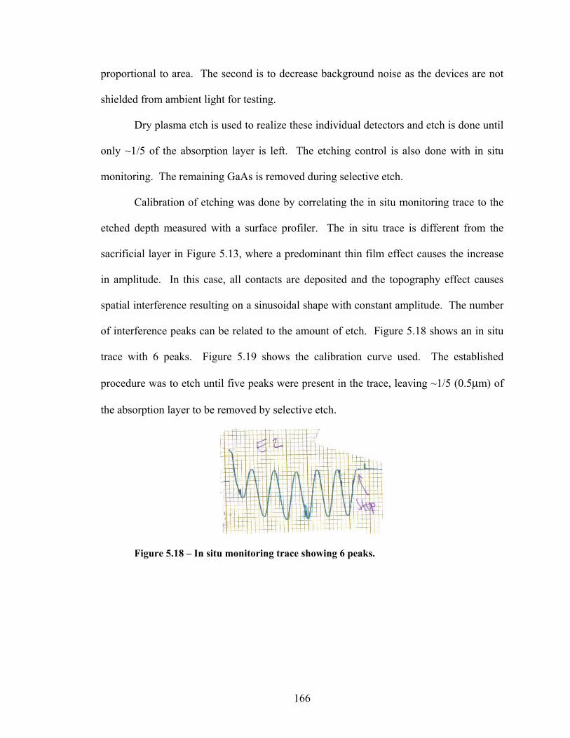
166
proportional to area. The second is to decrease background noise as the devices are not
shielded from ambient light for testing.
Dry plasma etch is used to realize these individual detectors and etch is done until
only ~1/5 of the absorption layer is left. The etching control is also done with in situ
monitoring. The remaining GaAs is removed during selective etch.
Calibration of etching was done by correlating the in situ monitoring trace to the
etched depth measured with a surface profiler. The in situ trace is different from the
sacrificial layer in Figure 5.13, where a predominant thin film effect causes the increase
in amplitude. In this case, all contacts are deposited and the topography effect causes
spatial interference resulting on a sinusoidal shape with constant amplitude. The number
of interference peaks can be related to the amount of etch. Figure 5.18 shows an in situ
trace with 6 peaks. Figure 5.19 shows the calibration curve used. The established
procedure was to etch until five peaks were present in the trace, leaving ~1/5 (0.5µm) of
the absorption layer to be removed by selective etch.
Figure 5.18 – In situ monitoring trace showing 6 peaks.

167
3 4 5 6 71.0
1.2
1.4
1.6
1.8
2.0
2.2
2.4
Etc
h de
pth
(µm
)
Number of peaks
Figure 5.19 – Depth of etching as function of the number of peaks present in the in situ monitoring trace. Measurements were done using a surface profiler.
5.3.b Oxidation
The purpose of the oxidation layer in the tunable detector is primarily for optical
confinement and mode filtering. The process is not critical and is straight forward for
such a thick layer of AlAs [112]. Even though it has many variables, as described in
chapter 3, it is very repetitive. However, it is important to remember that any different
furnace will give different oxidation rate. Moreover, repeatability is strongly related to
the operator and two different operators usually get two different rates because of slightly
different procedures on the open furnace/load sample/close furnace/open furnace /unload
sample sequence. Every time that the furnace is opened, temperature drops very fast and
this influences the oxidation rate to the extent that apertures with precision of 1µm cannot
be achieved.
The temperature used was 425ºC and open furnace/load sample/close furnace
sequence was timed to last 20s. Open furnace /unload sample was being done as fast as
possible so that it would return fast to 425ºC. The next open furnace/load sample/close

168
furnace sequence waited for the operation temperature to be achieved. The furnace used
was from Bandwidth9, Inc.
After furnace characterization, oxidation rate was consistently at 0.9µm/minute.
Oxidation has been carried out until heads with 18µm had their apertures totally closed.
The reason for this is that previous experience with 15µm heads required high numerical
aperture objectives to focus light into the device. However, optical coupling is less
sensitive if a small numerical aperture objective is used, as discussed in chapter 4. After
consistent oxidation runs of 20 minutes, only some of the 18µm heads were open and
none of the 20µm were closed, showing excellent repeatability.
Characterization of the aperture size was done with an IR CCD camera able to
“see” in the 900-1700nm. Even for this high reflective top mirror device, the aperture
could be clearly defined.
Unfortunately, the oxidation step was done too late in order to characterize the
effect of aperture on optical coupling. General detector characterization will be described
next together with the concept of a very compact biosensor.
5.4 Application
This section will show the characterization and performance results of the tunable
detector. The device can be used for several different applications such as biosensing,
spectroscopy, biometrics, optical interconnects and communications as part of drop or
monitoring systems. Because of this broad usage, characterization was done in a general
sense. However, the tunable detector was designed to biosensing, integrated to a
platform where biological reactions occur, what will be described next.

169
5.4.a Biosensing
Bioassays are important tools used to detect interactions of various biomolecular
complexes for pharmaceutical and biomedical applications. In addition, such analysis
methods can provide a deep understanding on how proteins, encoded by DNA, interact
with enzymes, inhibitors or other proteins. This is one of the most important next grand
challenges after the completion of the sequencing of the human genome [131-135].
In general, bioassay techniques can be put into two categories: labeling with
compounds (such as fluorescent, radioactive or colorimetric) and direct molecule
identification. For the majority of bioassays currently performed for life science research
and pharmaceutical screening, fluorescent or colorimetric chemical labels are commonly
attached to the molecules under study [31]. Labels can be readily visualized and the
measurement technique is simple. However, the attachment of labels may substantially
increase the assay complexity. It may also alter the functionality of molecules through
conformational modification or epitope blocking, which ultimately leads to errors in data
interpretation.
A label-free sensor is a bioassay tool that enables direct molecule detection, and it
is generally desirable due to its non-intrusive nature of detection. The sensor typically
consists of two parts. The first part is the binding surface, which is activated (coated)
with a known receptor molecule that has a high affinity to the molecules to be detected.
The second part is the detection mechanism that converts a recognizable molecular
binding event into a quantifiable signal. The activation step is always done a priori.
Assays using this method are much faster than the compound labeled ones, since no
additional incubation and activation steps for the attachment of labels are required. Thus,
the reduction in assay complexity results in faster screening or developing time.

170
Optical biosensors are a type of label-free biosensors that utilizes light as their
detection mechanism. They have several advantages, such as in situ real-time process
monitoring and high sensitivity to surface modifications, where most of the bioprocesses
take place [29-31]. Optical methods can be measured by different quantities, such as
angle, polarization, phase, amplitude, and frequency. The versatility of optical methods
is noticeable by the success of several devices such as surface plasmon resonance, output
grating couplers, ellipsometry, evanescent wave devices and reflectance interference
spectroscopy. Although bioassays using those methods are fairly sensitive, they are still
quite slow, bulky and expensive.
The proposed biosensor has been conceived to use novel integrated optoelectronic
devices in conjunction with a unique colorimetric guided-mode resonant (GMR)
diffractive grating structure as a surface binding platform. This approach can meet
stringent requirements of small size, high resolution, low power consumption, low cost
and the advantage of fabrication in 2D arrays.
5.4.a.1 Biosensor description
A guided mode resonant (GMR) filter has been optimized to work as a label-free
biosensor[38, 59, 136]. The GMR consists on a sub-wavelength grating surrounded by a
region with smaller index of refraction, as shown in Figure 5.20. The device is fabricated
by SRU Biosystems on a plastic (polyethylene terephthalate - PET) substrate by
imprinting a master grating into epoxy and curing [136]. High index dielectric is further
deposited. Thus, it is not only low cost but also disposable with minimum environmental
impact. Light incident onto the GMR in the normal direction can couple to the grating
structure under a certain resonance condition. This coupling results in a reflectance peak

171
with sharp spectral distribution. The resonant wavelength (λpeak) is varied by the
attachment of biomolecules, cells, and bacteria to its surface and depends critically on the
thickness (tbio) and refractive index (nbio) of those specimens. Figure 5.21 shows the
simulation for a typical GMR optical reflectance spectra using rigorous coupled wave
analysis (RCWA). Continuous deposition changes the tbio thickness, which in turn
changes λpeak. This system yields a very high resolution of 0.1 nm in protein thickness
change [38]. Hence, it is a high sensitive tool to track molecular/protein interactions once
desirable receptors are coated on the top layer. Since the wavelength regime is
determined by the grating period, it has been conveniently chosen to be around 850nm
based on available low cost optoelectronic components. The rest of the readout system,
including the optoelectronic components, is obviously reusable and measurements can be
repeated to improve accuracy.
Figure 5.20 – Guided mode resonant (GMR) filter. The device is made on a plastic (polyethylene terephthalate - PET) substrate by imprinting a master grating into epoxy and curing. High index dielectric is further deposited. Surface is very sensitive to attachment of biological material with thickness tbio and index nbio. After [136].
The previously reported detection system consists of a white light source that
illuminates the GMR sensor through an optical fiber that also collects the reflected light
to couple it to a spectrometer. Figure 5.22 shows the schematic of such arrangement.
The spectrometer signal is then monitored by a computer to detect wavelength shifts [38,
Polycarbonate Sheet
Cured Epoxy
PET substrate
cured epoxy
high n dielectric
nbiotbio
incident reflected
Polycarbonate Sheet
Cured Epoxy
PET substrate
cured epoxy
high n dielectric
nbiotbio
incident reflected

172
136]. Despite its high sensitivity, resolution will always be limited by the spectrometer
pixel wise nature and the trade-off between resolution and signal strength can limit
further improvements. Major challenges remain on how to make a low-cost, compact
and portable system that has high resolution and throughput.
846 848 850 852 854 856 858 8600.0
0.2
0.4
0.6
0.8
1.0
Ref
lect
ivity
Wavelength (nm)
tbio, nbio
Figure 5.21 – Simulation to illustrate the GMR filter spectrum for different thicknesses of material on top.
White Light
Mini-SpectrometerSi-APD Array
LiquidChamber
GratingRegion
Substrate
CollimationLens
Optical FiberProbe
Fiber
Polarizer
White Light
Mini-SpectrometerSi-APD Array
LiquidChamber
GratingRegion
Substrate
CollimationLens
Optical FiberProbe
Fiber
Polarizer
Figure 5.22 – Schematic of the sensor using white light and spectrometer configuration.
The tunable detector has been conceived to replace the spectrometer/computer in

173
an integrated way. The final sensor would be much smaller and still have high
resolution, low power consumption, low fabrication cost and the advantage of fabrication
in 2D arrays. Figure 5.23 shows the schematic of the sensor after integration of tunable
detector and GMR. A light emitting diode (LED) and tunable detector would replace
white light source and spectrometer, respectively. The transmission of the broadband
signal from the LED is depleted by the resonant reflection from the GMR and the tunable
detector can keep track of the dip. However, the area of the tunable detector head still
has to be increased in order to couple broadband signals. Current sizes would be able to
couple only the tunable laser for testing. Anyway, the system can be made very compact
and the resonant wavelength turns out to be irrelevant. Only shifts matter. The analysis
of the surface reaction can be made through the cantilever bias voltage to track the dip.
Processing such kind of data is extremely simple and done in the electrical domain.
Measurements can be completed in ms, much faster than “fast” biological reactions,
which occur in the units of second range. Thus, the built in circuitry for driving LED,
tunable detector and signal processing plus optical assembly can be made as small as
desirable, with the system size limited by the interface to the user. The interface would
have to provide the user with a visual display (output) and access to the GMR surface for
proteins input. The final system can have wrist-watch size or even smaller. Overall
power consumption would be very low what makes it easily portable.
There are essentially two ways to monitor the tuning voltage: lock to the dip or
continuous cantilever scanning. The latter is straight forward: the bias voltage has a
sawtooth format and the dip in detection is correlated to tuning voltage. Shifts in
resonance would change the position of the dip and also the bias voltage that corresponds

174
to the minimum detected current. Figure 5.24 shows the equivalent circuit for the tunable
detector with tracking capability. The p-contact is connected to a load and then to ground
so that the potential Vf floats with the detector current and causes the tuning potential to
change accordingly [21], locking the cantilever to the dip.
Biosensor Chip Plastic
High Index Dielectric
LEDCollimated Light(all wavelengths)
Transmitted light with resonant wavelength removed
Forward Diffracted Light
Backward Diffracted Light
Berkeley MEMSTunable DetectorIntegration of MEMS-Tunable Filter with a broad band detector
λ
ITrans
λλ p
ITrans
Idet
VtunVp
SRU Biosystems’
Plastic
Transmitted light with resonant wavelength removed
Forward Diffracted Light
Backward Diffracted Light
detector
Biosensor Chip Plastic
High Index Dielectric
LEDCollimated Light(all wavelengths)
Transmitted light with resonant wavelength removed
Forward Diffracted Light
Backward Diffracted Light
Forward Diffracted Light
Backward Diffracted Light
Berkeley MEMSTunable DetectorIntegration of MEMS-Tunable Filter with a broad band detector
λ
ITrans
λ
ITrans
λλ p
ITrans
λλ p
ITrans
Idet
VtunVp
Idet
VtunVp
SRU Biosystems’
Plastic
Transmitted light with resonant wavelength removed
Forward Diffracted Light
Backward Diffracted Light
detector
Figure 5.23 – Schematic of the sensor using LED and tunable detector configuration. The broadband signal from the LED is depleted by the resonant reflection from the GMR; the tunable detector can keep track of the dip.
Vt
Vf
Vd
Vt
Vf
Vd
Figure 5.24 – Tunable detector equivalent circuit with wavelength tracking. A load is inserted in between the p-contact and ground so that the potential Vf floats with the detector current and causes the tuning potential to change accordingly.

175
5.4.a.2 Tunable detector characterization
The characterization can be divided in three separate performances: mechanical,
optical and electrical. Mechanical characteristics show released parts performance such
as static droop and bending as function of voltage. Most of the mechanical
characteristics were shown in the previous chapter when discussing the folded beam
filter. Figure 5.25 shows the white light interferometry image of the tunable detector.
The device in the image shows a small negative droop (bending up) of less than 0.2µm
while the folded beam did not show any considerable buckle. This is probably because
the length of the beams is still below the critical length according to equation (4.1), and
that other structure has more rigidity with no free ends. However, the beam was still
released in two steps in this development.
Figure 5.25 – White light interferometry image of the tunable detector. This device shows a small negative droop of less than 0.2µm.
Optical characteristics were measured using the setup from Figure 5.26, also

176
designed to measure the integration with the GMR sensor. With this setup it is possible
to measure reflected and transmitted power as a function of input wavelength. A tunable
Ti:Sapphire laser is used and it can tune wavelength from 835nm to 985nm. Light is
collimated and tapped (beam splitter – BS1) to the optical spectrum analyzer in order to
keep track of wavelength. An achromatic lens is inserted after the beam splitter,
functioning in a similar way to a microscope eyepiece and minimizing chromatic
aberrations of the system. The insertion of this lens has allowed a much more stable
coupling while tuning, even though the tuning range is very short. This was an upgrade
from the tunable filter setup where coupling was unstable when tuning wavelength. All
measurements were normalized to the input power by splitting the input beam through
BS2 and measuring this reference signal at the same instant as the other signals (reflected
or detector current). A polarizer and the GMR sheet were supposed to be inserted in the
optical path by the time of integration. A third beam splitter, BS3, was required to use a
CCD for probing and placing the device in the beam path. The insertion of BS4 allows
reflected light to be measured, in complement to the current of the tunable detector.
Objective lenses with numerical aperture of 0.28 and 0.42 were used; however the larger
one has resulted in a linewidth spread in the measurements because of the varying angles
of incidence.
Careful optimization of coupling in real time was done again by applying a
sawtooth voltage to the cantilever beam while keeping the incoming wavelength
unchanged, similarly to what has been done with the torsional filter. The signal from the
tunable detector was coupled into an oscilloscope and the filter position was optimized
(x, y and z) until the best lorentzian like shape was obtained on the scope. After this fine

177
adjustment, the voltage on the cantilever could be kept constant at the desired value and
wavelength was scanned in order to measure the real linewidth of the filter transmission.
Ti:Saphire Tunable Laser
Collimation lens
BS1
Spectrum AnalyzerFiber
BS2
Reference Detector
Achromaticlens
M1
SRU filter
Polarizer
BS3BS4
CCD (top view)
Reflection Detector
Focusing Lens
Tunable Detector
P1
P3P2
M = mirrorBS = beam splitterP = probe
Ti:Saphire Tunable Laser
Collimation lens
BS1
Spectrum AnalyzerFiber
BS2
Reference Detector
Achromaticlens
M1
SRU filter
Polarizer
BS3BS4
CCD (top view)
Reflection Detector
Focusing Lens
Tunable Detector
P1
P3P2
M = mirrorBS = beam splitterP = probe
Figure 5.26 – Setup used for the optical characterization of the tunable detector integrated to the biosensor filter.
Figure 5.27 shows the measured typical spectral characteristics for the tunable
detector. Optimized coupling has eliminated the side mode at longer wavelengths but the
broadening shown on shorter wavelengths may have been caused by high order modes.
The achromatic lens is the element that contributes to this almost constant coupling as
function of wavelength. Tuning range was around 20nm, on average, and limited by poor
electrical isolation between mirrors. This was already discussed in the characterization of
the folded beam filter. When voltage is increased above ~6V the current across the
sacrificial layer increases and the device practically stops moving. If the electrical

178
isolation was better or softer beams have been designed, the device would move longer,
and consequently increase the tuning range.
849 852 855 858 861 864 867-0.2
0.0
0.2
0.4
0.6
0.8
1.0
norm
aliz
ed d
etec
tion
wavelength (nm)
6.3V 5.9V 5.7V 5.4V 4.5V 2.8V
Figure 5.27 – Measured spectral characteristics for the tunable detector.
Figure 5.28 shows the transmission spectrum for the torsional filter at 856 nm.
Linewidth is very sharp and a lorentzian fit shows 0.4nm of FWHM. Average value of
linewidth was 0.8nm, without optimized coupling at all wavelengths. Higher resolution
in wavelength for a better trace was limited by the step motor used to tune the
Ti:Sapphire laser.
Electrical characteristics of the detector were measured in a standard way. Figure
5.29 shows a typical Current-Voltage (IV) curve for the tunable detector. This curve is
obtained in the dark, at room temperature, and the current at -5V is usually defined as
dark current (Id). In this case, Id was 4µA but typical range was from 1µA to 50µA. P-i-
n diodes can have dark current as low as 10pA, as the case for the commercial device
from LuxNet Corporation that grew the wafer used for the tunable detector. Id is
originated from thermal generation of electron-hole pairs inside the device and is
proportional to the square root of the applied voltage (of course it is also function of

179
temperature). Id is then proportional to the device area and the high values measured are
related to the still large area, even after the separation of the detectors in the die. The
value mentioned above for the commercial device is for a circular detector with diameter
of 100µm while in the tunable detector case the entire mesa, defined by wet etch plus
contacts (>5X larger), contributes to Id. Finally, based on the IV information, the device
was reversed biased with 2V during operation. Noise level during normal operation
(lights on) was around 25µA.
852 854 856 858 860
0.0
0.2
0.4
0.6
0.8
1.0
∆λ=0.4nm
norm
aliz
ed d
etec
tion
wavelength
5.7V Lorentzian fit
Figure 5.28 – Transmission spectrum for the torsional filter at 856 nm. Linewidth is very sharp and a lorentzian fit shows 0.4nm of FWHM. Optimized coupling has eliminated the side mode at longer wavelengths but broadening on shorter wavelengths may have been caused by high order modes.
Capacitance as function of reverse bias was not measured as this value is only
relevant for high speed measurements. Forward resistance can also be derived from the
IV curve and the average value is 40Ω, slightly larger than commercial products (~10Ω).
Detector responsivity was measured in the dark and found to be 0.2A/W, which is a good
value facing the GaAs limit of 0.65A/W (commercial products usually achieve 0.5A/W).

180
-8 -6 -4 -2 0 2
1E-8
1E-7
1E-6
1E-5
1E-4
1E-3
Abs
olut
e cu
rren
t (A
)
Voltage (V)
Figure 5.29 – Typical current-voltage (IV) characteristic for the tunable detector.
Table 5–1 Summary of tunable detector average characteristics.
Tuning range 20nm
Tuning voltage 0 - 8V
Linewidth 0.8nm
Responsivity 0.2A/W
Forward resistance 40Ω
Dark current @5V <50µA
While the characterization and fabrication development was still proceeding, with
successive improvements on final devices, the Ti:Sapphire tunable laser went out of
service. Some other options, that not a tunable laser, would be white light or LED as
light source. However, these low coherence sources can not be collimated or focused to
the spot size required to couple light into the tunable cavity. Another change would be
required: that the sizes (head and eventually gap size) were increased accordingly to the

181
broadband source. Moreover, it would mean to change the entire lithography mask set
and also the characterization optics. The choice was to wait until the system comes back
to work.
In the mean time, a conceptual alternative approach was launched. The light
source would be replaced by a tunable VCSEL and tunable detector would be replaced by
a broadband p-i-n detector. This turned out to be a very fortunate fact as the tunable laser
has shown to be much more attractive than the tunable detector. In the end, this change
of gears condemned the tunable detector integration to the GMR never to happen.
The optical characterization of the variable apertures was not done either, as the
focus was on biosensing not on coupling. The oxidation development was done in
parallel to the tunable laser integration and its importance was decreasing in the same
proportion that the laser approach was succeeding. However, this optical confinement
and linewidth enhancement of filters would be a very good topic for further study.
5.5 Summary
This chapter presented specific details about the design and fabrication of a
tunable detector that can be applied not only to biosensing but also to several other
applications such as WDM communications systems or spectrosocpy. The topology
chosen was the cantilever Fabry-Pérot tunable filter integrated to a p-i-n detector, which
can have uniform responsivity across the tuning range. Fabrication is similar to the
tunable filter but the absorption layer has further to be vertically etched to separate
devices in the same die and oxidation was performed to control the aperture of the optical
cavity.
The detector was to be integrated to a guided mode resonant (GMR) filter, by

182
replacing white light and spectrometer/computer, and providing a portable biosensor with
high resolution, low power consumption, low cost and the advantage of fabrication in 2D
arrays. The GMR serves as a surface binding platform and tunable detector/LED as the
reading mechanism.
The detector was characterized according mechanical, optical and electrical
properties. Final performance yielded smaller tuning range (20nm) than designed (30nm,
in the range 835-865nm) due to a leak current in between mirrors. Electrical and
mechanical characteristics were very good.
The problem with the Ti:Sapphire laser cut short the characterization and opened
space to another biosensor approach using a tunable VCSEL, which has shown to be a
much more attractive option, to be presented in the next chapter.

183
Chapter 6 Tunable VCSEL
6.1 Introduction
In the previous chapters, passive tunable micromachined devices with wide tuning
range and innovative mechanical structures have been presented. This chapter discusses
the usage of an active device, vertical cavity surface emitting laser (VCSEL), into the
development of a very sensitive optical biosensor. It makes directly usage of tunable
VCSELs but tunability of the devices is achieved through bias current and temperature
[137, 138], differently than the devices previously discussed, which use micromachining
techniques. However, micro-electro-mechanical (MEM) VCSELs can readily replace the
ones used here and substantially increase the dynamic range of the biosensor [47, 57, 58].
Preceding chapters have described design and fabrication in detail. The same
methods are applied to VCSELs but special design has to be done to the active region.
DBR mirrors also have to suffer some modifications, such as design for current
confinement and graded transition between different material compositions, in order to
improve thermal and electrical characteristics of the device [97]. The overall technology
is now mature and detailed description has been subject of several textbooks [2-6].
Hence, this chapter will limit the discussion to integration of devices to the biosensing
systems.
Even though some devices have been designed and fabricated, the ones that have
been used are commercial. Several reasons would justify this option but the main one
was timing. As mentioned in the last chapter, the systems here described were born as an
alternate approach to the tunable detector and it can only be justified if it can be

184
implemented faster than the previous. However, the development of a reliable fabrication
process, from epitaxial growth (which can always be contracted, as before) to final
characterization, may take months of academic research and the final result may still be
uncertain. Price is another factor, as market price for good quality single-mode VCSELs
is around US$35.00 each, which is much less than would take to fabricate such devices.
Moreover, commercial devices have fairly good characteristics and are already packaged
in a very convenient way for current and temperature control. Furthermore, the lasing
wavelength of the fabricated devices did not match the one required for integration to the
guided mode resonator (GMR).
The focused characteristics for the sensor presented in this chapter are label-free
detection, compactness and portability. Besides, it will be shown that the approach used
here also provides high sensitivity, low power consumption and low cost. The ultimate
goal, however, is to generate new systems that can enable new benefits to society.
6.2 Sensor Description − tunable VCSEL and GMR biosensor
The guided mode resonator (GMR) has been already described in the previous
chapter. Although the biosensor that integrates the GMR with white light/spectrometer
reading system, also described before, has high sensitivity through computational signal
processing, its resolution will always be limited by the spectrometer pixel wise nature.
The signal-to-noise ratio is low and the trade-off between resolution and signal strength
can limit further improvements. Figure 6.1 illustrates this trade-off, where increased
resolution of the spectrum analyzer is always together with a lower overall detected
power due to constant power density. The tunable detector approach from last chapter is
a very good alternative to make a low-cost, compact and portable system that has high

185
resolution and throughput. However, it may require complicated optical coupling
mechanism, similar to what has been shown in chapter 4 for the tunable filter, and
linewidth may still suffer from nonuniform coupling as function of wavelength.
840 842 844 846 848 850 852 854 856
Ref
lect
ed P
ower
(a.u
.)
Wavelength (nm)
OSA resolution 1nm OSA resolution 0.1nm
Figure 6.1 – White light trace showing the trade-off between resolution and signal strength.
The idea behind the sensor is still the same: monitor the shift of the GMR
resonance. Even though the tunable detector integration was not completed, early
experiments have shown that measurements cannot go through the GMR because of the
resultant lens effect from the surface of the liquid inside the wells. The wells have about
8mm of diameter and the curvature of the liquid surface deviates the light beam and
contributes to poor transmission and coupling. Similar problem happens to dry samples,
where deposited material works as a scattering source.
Here, the detection system of the proposed VCSEL based biosensor utilizes a
tunable single-mode 850nm VCSEL and two p-i-n detectors, as shown in Figure 6.2.
Optoelectronic devices are placed under the GMR and biological reactions occur on the
top. Light output from the VSCEL is already polarized and there is no need for a

186
polarizer if the cavity is previously aligned to the grating lines. In order to scan for the
peak resonant position λpeak, the VCSEL wavelength is tuned by sweeping its bias
current, causing a rapid thermal effect that shifts the lasing wavelength [137]. Detector 1
is positioned to measure the reflected light from the GMR substrate, while detector 2
provides the normalization current for the incident power, since the VCSEL output power
also varies with the bias current. Thus, the ratio of the two detector signals is used to
monitor the reflection peak. Varying the laser bias current provides a fast but narrow
range (2−3 nm) tuning of the VCSEL wavelength. Temperature tuning is also used to
augment the tuning range, extending it to 8−9nm. The typical wavelength dependence
for temperature and current tuning for a VCSEL is 0.08nm/ºC and 0.4nm/mA,
respectively. Even though our current design of the VCSEL based biosensor may be
limited to those biomolecular interactions that cause small wavelength shifts, a larger
dynamic range can also be obtained by means of two different approaches: tunable
detector and MEM tunable VCSEL. In the first one, the system from the previous
chapter can be implemented (LED as source and tunable detector as monitoring
mechanism). In the second approach, the current-tuned VCSEL can be replaced by a
micro-electro-mechanical tunable VCSEL [58, 139]. Both approaches can easily enable
about 30nm of peak wavelength scanning.

187
PIN Detector 2(Reference)
Beam ExpansionCollimation
Tunable VCSEL
PET Substrate
Beam Splitter
PIN Detector 1 (Reflection)
Cured Epoxy
high “n” dielectricbiobio , nt
GMR
Figure 6.2 – Biosensor with VCSEL based measurement system. A tunable VCSEL and two p-i-n detectors work as a readout system for a plastic guided-mode resonant (GMR) filter that is the binding surface. Peak reflectivity from the GMR is detected by correlating maximum normalized detector current with laser bias current.
Besides the advantage in compactness, sensitivity is greatly enhanced by using a
laser rather than a broadband source (white light or LED). Since the sharp reflection
peak is due to the resonance from the GMR and it is very sensitive to incident angle [59],
a coherent light source with smaller diffraction and a higher signal-to-noise ratio can
improve the sensitivity of the system.
Furthermore, the analysis of the surface reaction is all done in the electrical
domain, thus simplifying data processing. Using the one-to-one correspondence between
the laser bias current and lasing wavelength, at a given temperature, the normalized
detected current versus wavelength can be directly mapped. From the mapping, the
spectral response of the GMR biosensor as a function of wavelength can be deduced, and
the peak resonant wavelength can be determined. Moreover, the electrical circuitry, for
signal processing and driving the VCSEL and p-i-n detector, and optical assembly can be
made very compact.

188
Finally, as all technologies being used are naturally 2D, the system can be
extended to an array format, where different cells can be activated to respond to different
proteins. In this configuration, laser and detector can be fabricated in the same wafer
[140] and this array topology can also be made even smaller and portable, something
similar to a cellular phone.
6.3 Sensor characterization
In order to characterize the biosensor system apart from the context of a particular
biomolecular assay, two experiments were performed. The purpose of them was to
investigate resonant wavelength shifts due to changes in nbio and tbio respectively. With
the setup previously described, a 3x5in2 GMR plastic sheet was cut and bonded to the
bottom of a bottomless 96-wells microplate [136] so that the liquid solutions can be
easily deposited on top of the GMR sheet.
The first experiment measured the wavelength shift as function of the refractive
index variation of the specimen deposited on top of the grating. Fluids with various
refractive indices were deposited into the wells and the corresponding GMR spectral
response was measured. The liquids used were standard matching fluids from Cargille
Laboratories with the precision of ±0.0002 in index. A very low index of 1.280 (Galden
fluid), from Solvay Solexis, was also used. The measurements were all performed in the
same well. The procedure consisted on pipetting 100µl of index matching fluid into the
well and scanning the laser bias several times. The fluid was pipetted out of the well and
the well was rinsed with isopropanol and water before pipetting in the next fluid. Figure
6.3 shows the average spectral shifts of the resonance for four different index matching
fluids, and the wavelength scale is used in order to compare traces acquired at different

189
operation temperatures. The VCSEL based biosensor system shows a very high
sensitivity to small changes in the surface refractive index, as illustrated in Figure 6.4.
The wavelength dependence is linear and an index change ∆n < 0.001 can be easily
resolved.
846 848 850 852 854 856 858 860Wavelength (nm)
Tran
smitt
ed P
ower
(a.u
.)
n=1.280 n=1.292 n=1.298 n=1.305
Figure 6.3 – Measured spectral shift of the resonance as function of index of refraction of the solution on top of the GMR.
1.275 1.280 1.285 1.290 1.295 1.300 1.305 1.310850.0
850.5
851.0
851.5
852.0
852.5
853.0
853.5
854.0
Wav
elen
gth
(nm
)
Index of refraction
Figure 6.4 – Wavelength shift as function of index of refraction of the solution on top of the GMR. Index changes ∆n < 0.001 can be easily detected by this system.
Measurements of the GMR spectral response were also performed using white

190
light and spectrum analyzer. Figure 6.5 shows the result and comparison with Figure 6.3
confirms an enhanced sensitivity because of the coherence of the light source. The GMR
response is very sensitive to incident angle and even small angles with respect to the
normal broaden the linewidth of the resonance [59, 141, 142]. White light can be seen as
the combination of monochromatic sources with a wide distribution of k vectors in
different amplitudes and directions, which causes the various incident angles. On the
other hand, VCSEL is basically a monochromatic source with a well defined k , yielding
a sharper resonance and increasing sensitivity.
846 848 850 852 854 856 858 860
n=1.280 n=1.292 n=1.298 n=1.305
Tran
smitt
ed P
ower
(a.u
.)
Wavelength (nm)
Figure 6.5 – White light measurements of the spectral shift of the resonance as function of index of refraction of the solution on top of the GMR.
The second experiment measured thickness variations of the specimen deposited
on top of the grating. The experiment consisted of the deposition of successive layers of
polyelectrolyte polymers and the measurement of the GMR spectral response for each
layer. Polyelectrolytes are long molecules that can be either positively (polycations) or
negatively (polyanions) charged and bind through electrostatic attraction. In principle,
the adsorption of molecules carrying equal charges leads to charge reversal on the

191
surface. This has two important consequences: (i) the repulsion of equally charged
molecules and thus self-regulates the adsorption to a single layer; and (ii) the ability for
an oppositely charged molecule to be adsorbed in the second step, on top of the first one.
Cyclic repetition of adsorption/wash steps (positively/negatively charged) leads to the
formation of multilayer structures. Figure 6.6 illustrates the basic buildup sequence. The
linear increase of film thickness is a polyion property, independent of the surface [143].
Figure 6.6 – Schematic of the film deposition process using slides and beakers. (A) Steps 1 and 3 represent the adsorption of a polyanion and polycation, respectively, and steps 2 and 4 are washing steps. (B) Simplified molecular picture of the first two adsorption steps, depicting film deposition starting with a positively charged substrate. After [143].
The polyelectrolytes used in this experiment were cationic poly-ethyleneimine
(PEI), anionic poly-sodium styrenesulfonate (PSS) and cationic poly-allylamine
hydrochloride (PAH), all obtained from Aldrich. The polyelectrolytes were dissolved in
a buffer solution of 0.9M of NaCl, at a concentration of 5mg/ml. The same buffer
solution was also used to rinse the well surface after the adsorption of each monolayer.
An initial base layer of cationic PEI was deposited on the GMR surface by
pipeting 100µl of PEI solution into a microplate well. The PEI polymer has very large

192
charge density and is suitable for this first layer binding to the sensor surface. After 5
minutes of incubation period, the PEI solution was removed, the well was rinsed with the
buffer solution, and the spectral response was measured with buffer inside the well by
scanning the VCSEL bias current. The same deposition/wash procedure was repeated for
alternating cycles of PSS and PAH polymers. Since the growth of the polyelectrolyte
polymers is self-limiting, the thickness of each layer is found to be ~50Å (10% error
expected due to molecular nonuniformity) [136, 144].
842 844 846 848 850 852 854 856
PSS 2PAHPSS 1
PEI
Ref
lect
ivity
(a.u
.)
Wavelength (nm)
PEI PSS 1 PAH PSS 2
Figure 6.7 – Spectral shift of the resonance due to changes in polymer thickness on top of the GMR.
The spectral shifts of the resonant wavelength, as layers of polyelectrolyte
polymers were being deposited, is shown in Figure 6.7, where one-to-one correspondence
between the bias current and wavelength is again used. The peak resonance shift can be
plotted as a function of deposited polymer thickness, as shown in Figure 6.8. The
±0.1nm error bars on wavelength are due to the resolution limit in the measurement
system. Thus, the biosensor has the high sensitivity to resolve much less than 10Å of
thickness variation on top of the GMR surface, as can be seen from the linearity of the

193
curve obtained in Figure 6.8.
-2 0 2 4 6 8 10 12 14 16
847
848
849
850
851
852
Peak
Wav
elen
gth
(nm
)
layer thickness (nm)
Figure 6.8 – Wavelength shift as function of polymer thickness on top of the GMR. The system can resolve much less than 10Å of thickness variation.
The above results had the property that the testing sample resulted in complete
coverage of the grating surface, even for the polymers [144]. However, simulations show
that GMR will respond even for partial coverage, which is the case for real proteins.
Figure 6.9 shows the simulation of partial coverage of the grating surface with same
percentages on top and bottom of the grating. The simulation takes into account
deposition of 100nm of material with index of refraction n=1.5. The response (peak
shift) will be proportionally smaller, with linear dependence until 50% of coverage and
parabolic below this value. Linewidth of the resonance will be almost constant for any
level of coverage. Figure 6.10 shows the simulation for 4 different cases: no deposited
material (0%), deposition only on top of the grating (45%), only on bottom (55%) or full
coverage (100%). These cases are not very likely to happen but illustrate that the device
will work even when the bottom lines of the grating are narrower than the surface
activation molecules (a virus, e.g.).

194
0 20 40 60 80 1000
2
4
6
8
10
12
nm
Surface coverage (%)
Wavelength shift Peak linewidth
Figure 6.9 – Simulation of partial coverage of the grating surface with same percentages on top and bottom of the grating.
0 20 40 60 80 1000
2
4
6
8
10
12
nm
Surface coverage (%)
Wavelength shift Peak linewidth
Figure 6.10 – Simulation of partial coverage of the grating surface with no deposited material (0%), deposition only on top (45%), only on bottom (55%) or full coverage (100%).
6.4 Protein Binding Assays
Following the previously sensor characterization, the application of the VCSEL
based label-free biosensor measurement system for protein-protein binding
immunoassays was investigated. The characterization of protein interactions consists of
the detection of the binding between an antibody – goat anti-mouse immunoglobulin

195
(IgG), and an antigen – mouse immunoglobulin (IgG), as shown in Figure 6.11. The
proteins were obtained from Jackson ImmunoResearch, each being affinity-purified and
chromatography-purified, respectively. Three different experiments were performed, in
order to study the performance of the biosensor system: ELISA, dynamic binding and
static concentration. ELISA stands for enzyme-linked immunosorbent assay, which is a
standard clinical method that requires additional labeling used to determine the antigen
concentration in unknown samples. The dynamic experiment enables the quantification
of the antibody-antigen binding as a function of time. Meanwhile, the static experiment
quantifies the resonant wavelength shift as a function of mouse IgG concentration,
similarly to ELISA but faster because requires a small number of incubations.
PIN Detector 2(Reference)
Beam ExpansionCollimation
Tunable VCSEL
PET Substrate
Beam Splitter
PIN Detector 1 (Reflection)
Cured Epoxy
high “n” dielectric
GMR
Antibody Block Antigen
PIN Detector 2(Reference)
Beam ExpansionCollimation
Tunable VCSEL
PET Substrate
Beam Splitter
PIN Detector 1 (Reflection)
Cured Epoxy
high “n” dielectric
GMR
Antibody Block Antigen
SENSOR
Goat Anti-Mouse IgG(Antibody)
Goat Serum (Block)
Mouse IgG (Antigen @ various concentrations)
SENSOR
Goat Anti-Mouse IgG(Antibody)
Goat Serum (Block)
Mouse IgG (Antigen @ various concentrations)
SENSOR
Goat Anti-Mouse IgG(Antibody)
Goat Serum (Block)
Mouse IgG (Antigen @ various concentrations)
SENSOR
Goat Anti-Mouse IgG(Antibody)
Goat Serum (Block)
Mouse IgG (Antigen @ various concentrations)
Figure 6.11 – The configuration of VCSEL based biosensor and the sequence of protein layers. The protocol follows a standard mouse IgG capture immunoassay, as shown on the right.
The protocol for all three experiments followed a standard mouse IgG capture
immunoassay. First, the antibody protein was deposited by applying 100µl/well of goat
anti-mouse IgG (1.8µg/ml), which was diluted in phosphate-buffered saline (PBS)
solution, and it was incubated for 10-12 hours at 4ºC. The incubation period allowed

196
sufficient time for the mouse IgG protein to bind to the GMR sensor surface and the low
temperature favors the binding. Then the excess solution was removed and the wells
were washed with PBS-Tween. Next, normal goat serum (200µl/well of 3% goat serum
in PBS) was applied to block the vacant spots of the sensor surface not covered by the
antibody and it was incubated for 2 hours at room temperature. This blocking step is
required to minimize the false-positive errors from the measurements, since the antigen
protein might bind to the exposed sensor surface as well as to the antibody protein.
Following the removal of the block solution and wash of the wells, the spectral response
of the GMR sensor was measured with PBS inside the wells, and this peak resonant
wavelength became the reference of comparison for the subsequent antigen
measurements, on dynamic and static experiments. Lastly, the antigen protein was
deposited by applying 100µl/well of mouse IgG at various concentrations and it was
incubated at 4ºC for ELISA and at room temperature for the others. Measurements were
taken during and after the incubation period for the dynamic and static experiments,
respectively.
Two ELISA assays were performed in parallel, one in a GMR plate and another in
a standard polystyrene plate. This was to compare both responses and use the
comparison to calibrate further results, if needed. It was also used to verify binding of
the first antibody to the GMR surface and test the surface activation. ELISA requires two
additional steps than those described above and the protocol also recommends that mouse
IgG (antigen) is incubated for 10-12hs at 4ºC. The additional required steps are a second
antibody (which has the labels) incubation and development of the labels. This second
labeled antibody incubation is done after removing and washing the previous solution

197
that had antigen, and it specifically binds to the antigen. More than one binding per
antigen may occur, resulting in amplification. This double antibody binding is also called
sandwich ELISA. The label of the secondary antibody, usually an enzyme, converts the
colorless substrate to a colored product. In this case, the enzyme is p-nitrophenyl-
phosphate (pNPP) which is converted to the yellow p-nitrophenol by alkaline
phosphatase. This colored product is measured on an ELISA plate reader as function of
the optical density at some specific wavelength, in this case yellow. Figure 6.12 shows
optical density at λ = 560nm, as given from the ELISA reader for both GMR and
standard polystyrene ELISA plate. The GMR has more sensitivity than the polystyrene
plate as seen from the larger range of optical density. However, it had a strong
background noise due to interference of the grating with the read out system. The results
shown were normalized with respect to the background for both plates. The nearly
similar response of the two plates shows that further calibration of the GMR results is not
necessary.
1E-9 1E-8 1E-7 1E-6 1E-50.00
0.25
0.50
0.75
1.00
1.25
1.50
1.75
2.00
Opt
ical
den
sity
(a.u
.)
Antigen (mouse IgG) concentration (g/ml)
ELISA plate GMR
Figure 6.12 – Optical density at 560nm as given from the ELISA reader for both GMR and standard polystyrene ELISA plate.

198
In the dynamic measurement, the kinetics of the antibody-antigen binding for
three different mouse IgG concentrations, with each repeated for three different wells,
was continuously monitored during the incubation period with the time resolution of 5
seconds. Figure 6.13 shows the averaged normalized surface binding curves for different
concentrations of mouse IgG as a function of time, obtained by integrating the difference
of the GMR spectral response for the starting time and that of a given time. It should be
noted that the saturation level is antigen concentration dependant, and the normalization
here enables the comparison of surface binding time for different antigen concentrations.
If required, this technique allows for ultrafast, dynamic monitoring in the ns range, as the
VCSEL can be modulated in the GHz range. As expected from results of typical kinetic
binding experiments, most of the protein binding occurred rapidly at the beginning of the
incubation, followed by a gradual saturation. As indicated in Figure 6.13, the time for
80% (of the saturation level for each concentration) surface binding time for goat anti-
mouse IgG and mouse IgG proteins is around 300s, with dependence on the mouse IgG
concentration. Low concentrations take more time to saturate than high concentrations.
These results can also be used to characterize the time needed for an antibody to trigger
its immuno-response to the respective antigen.

199
0 400 800 1200 1600 20000
20%
40%
60%
80%
100%
Time (sec)
Nor
mal
ized
Sur
face
Bin
ding
(a.u
.) 1 ng/ml: 345 sec 10 ng/ml: 304 sec100 ng/ml: 245 sec
1 ng/ml 10 ng/ml
100 ng/ml
Time for 80% Surface Binding
Figure 6.13 – Dynamic measurement: surface binding versus time for different antigen concentrations. Most of the protein binding occurred rapidly at the beginning of the reaction, followed by a gradual saturation. The 80% surface binding time is about 300s, with a slight dependence on the mouse IgG concentration.
In the static measurement, the resonance shift resultant from the antibody-antigen
binding was monitored for eight wells in the microplate. After the removal of the block
solution, mouse IgG solution was applied to each of the wells with the smallest
concentration of 1pg/ml, and it was incubated for 1.5 hour at room temperature. The
solution was removed and the GMR biosensor’s spectral response was finally measured
with PBS inside the well. Thus, any signal masking related to variation of index of
refraction due to concentration of the solution was avoided and only the binding effect
was considered. Then PBS was removed and the next mouse IgG solution of 10pg/ml
was added to the wells. The incubation-measurement-removal sequence was repeated for
different mouse IgG solutions with their concentrations increased by 10X each time, up
to 10µg/ml. Figure 6.14 shows the average of the peak resonant wavelength shifts for the
eight wells, as a function of mouse IgG concentration. The high sensitivity of the
VCSEL based measurement system is shown from its ability to detect the smallest

200
concentration of 1pg/ml. As both the antibody and antigen IgG proteins have their
molecular weight approximately 150 kDalton, a sensitivity of 1 pg/ml is equivalent to 6.7
fM/l (femto-Mol/liter). The nearly saturation observed above 10ng/ml was caused by the
depletion of the available antibody-antigen binding sites, and it is expected that the
saturation concentration can be increased by depositing higher concentration of the
antibody at the first step or by simply using different wells for each concentration. This
last procedure would rely on very good uniformity of the GMR grating.
10-12 10-10 10-8 10-6 10-40
0.1
0.2
0.3
0.4
0.5
0.6
Concentration (g/ml)
Wav
elen
gth
Shi
ft (n
m)
Figure 6.14 – Static measurement: average resonant wavelength shift as function of the antigen concentration. The high sensitivity of the VCSEL based measurement system is shown from its ability to detect the smallest concentration of 1pg/ml or 6.7 fM.
Finally, the proposed structure from Figure 6.11 can be built into a very compact
and cheap biosensor without sacrificing sensitivity. Operation would have a reusable
platform, including optical, electrical and display parts, and the GMR sheets can be easily
replaced for sequential analysis. The overall cost for this system would be very low,
residing much more on packaging than on parts.
The results presented are not only encouraging but also fantastic. The level of
detection (6.7fM/l) is more than one order of magnitude better than state of art methods

201
that employ techniques well known by their high sensitivity such as surface plasmon
resonance (SPR) and reflectance interference spectroscopy [31, 145]. Recently, portable
sensors using SPR have been reported to achieve sensitivity of 100fM/l with binding
amplification and 70pM/l without amplification [146, 147]. Another candidate technique
for compact sensors with multidetection capability, diffractive gratings, has not reported
better sensitivity results than 0.5ng/ml [148]. Moreover, the VSCEL biosensor is much
more sensitive and faster than ELISA, which is the most used method for clinical analysis
[149].
6.5 Summary
This chapter presented a label-free and compact biosensor using VCSEL. The
devices used were commercial VCSELs, tuned by both current and temperature.
The sensor has a very simple configuration, consisting of a tunable VCSEL, a
plastic guided-mode resonant (GMR) surface, and two pin detectors. The device has
shown to be highly sensitive to surface modifications, with the ability to detect thickness
variations 10Å and <0.001 of change in the index of refraction. Protein binding tests,
consisting in standard mouse IgG capture immunoassay, were done for dynamic and
static experiments and the system has shown extremely high sensitivity, detecting even
an extreme low concentration of 1pg/ml (6.7femto-Mol/l).
All technologies being used on the sensor are naturally 2D and the system can be
readily extended to an array format. Then, different cells can be activated to respond to
different proteins and throughput can be very high. Thus, these compact, label-free, high
sensitivity, low power, low cost and potentially portable biosensors systems can enable
enormous new benefits to society such as virus detection in isolated communities in

202
Africa, fast screening on drug discovery and air/water quality monitoring in disaster
areas.

203
Chapter 7 Conclusion
7.1 Summary
This dissertation described design, fabrication technology, characterization and
applications of tunable filter, detector and VCSEL, all fabricated in GaAs and
monolithically tuned. Each one of the chapters in this dissertation had a summary at the
end. Thus, it does not make sense to repeat the same ideas again and again but, however,
the main achievements should be pointed as they figure among the best around the world.
Chapter 2 covered the basic concepts in the design of micro-mechanical tunable
optoelectronic devices. A new sub-wavelength grating mirror, with clear advantages for
long wavelength applications, was presented as an option to the conventional distributed
Bragg reflectors. General design rules, valid form short to long wavelengths, were
organized in the form of a flux diagram.
Chapter 3 gave all processes used on the fabrication of GaAs devices in general.
Sub-wavelength grating mirror was fabricated in silicon in excellent agreement with
theory.
Chapter 4 presented specific details on the design and fabrication of tunable filters
applied to communications and IR imaging. A record tuning range of more than 100nm
was achieved with a torsional micro-mechanical tunable optical filter, which is also free
of damages resulting from capacitor discharge and does not cause any power penalty into
optical links. A folded beam filter structure, which has large ratio of detector to pixel
area and convenient topology for implementation of 2D array with matrix addressability,
was demonstrated for application on IR imaging.

204
Chapter 5 described the conception of a tunable detector to be integrated to a
guided mode resonant (GMR) filter and provide a portable biosensor with low cost, high
resolution, low power consumption, and the advantage of fabrication in 2D arrays. The
detector topology consisted on a Fabry-Pérot tunable filter with controllable aperture
integrated to a broadband p-i-n detector. A tool problem prevented the full integration
and an alternate approach with tunable VCSEL turned to be much more attractive.
Chapter 6 presented a novel label-free compact and portable biosensor using
VCSEL. The system uses a tunable VCSEL based measurement system integrated to a
GMR. The approach can provide high sensitivity, dynamic and static measurements, low
power consumption and low cost. The sensor is particularly sensitive to low
concentrations, detecting protein concentration as low as 6.7femto-Mol/l.
7.2 Potential Future Work
The work presented here is far from being complete and there are still many
exciting topics that are worth investigating. The SWG approach for mirrors has proved
to be effective, easy to fabricate and more advantageous for middle and long wavelength
infrared applications. The next logical step is to fabricate devices that incorporate SWG
mirrors and are specifically designed for the wavelengths of interest. These devices
would then be integrated to a focal plane array in order to provide real-time hyperspectral
images.
Another interesting experiment would be to conclude the characterization of the
optical confinement and linewidth enhancement of filters with respect to the cavity
aperture. The exact same structure designed for the tunable detector can be used for this
purpose.

205
The most exciting perspectives, however, are in the direction of the VCSEL
biosensor. The development of 2D arrays is a natural step as all technologies involved
are naturally 2D. Figure 7.1 illustrates a top view of an array of tunable VCSELs and p-i-
n detectors under the GMR sensor, with the lasers and detectors on the same chip and
normal incidence is used. The wafer can be designed for the laser and detector to be
made in the same chip. The diffraction of the laser beam illuminating the sensor and
reflecting back is sufficient to hit the detector. The final assembly would be extremely
compact and different cells can be activated to respond to different proteins and
throughput can be very high. The simultaneous measurement of a larger biomaterial area
is a new functionality that no other existing technique can provide.
SensorChip(above)
VCSEL/detectorChip (below)
Receptor Molecule Spots
VCSEL
detector
VCSEL/detectorChip (below)VCSEL detector
Focusing lens
SensorChip(above)
(a)
(b)
SensorChip(above)
VCSEL/detectorChip (below)
Receptor Molecule Spots
VCSEL
detectorSensorChip(above)
VCSEL/detectorChip (below)
Receptor Molecule Spots
VCSEL
detector
VCSEL/detectorChip (below)VCSEL detector
Focusing lens
SensorChip(above)
VCSEL/detectorChip (below)VCSEL detector
Focusing lens
SensorChip(above)
(a)
(b)
Figure 7.1 – Tunable VCSEL and resonant cavity detector array integrated to the GMR sensor. The sensor will be on top of the laser and separate locations of the sensor can analyze different proteins simultaneously.
Experiments with real virus, such as HIV and dengue, are very likely to happen in
the near future. The sensor has proved to be suitable for fast label-free clinical analysis

206
(similar to an ELISA without labels) and specific reagents for the protocol are under
development in several places, including Public Health and Immunology Departments at
UC Berkeley.
Another interesting breakthrough would be the integration of all electronics,
optics and optoelectronics devices into a compact mount. Figure 7.2 shows a picture of
the 96-wells plate with GMR and a prototype of an electronic driver for VCSEL and
detectors. Optics and optoelectronic devices can be inserted in between and use a XY
positioning system to allow inspection of all 96 wells.
Figure 7.2 – Picture of the 96 well plate with GMR and a prototype of an electronic driver for VCSEL and detectors. Optics and optoelectronic devices can be inserted in between and use a XY positioning system to allow inspection of all 96 wells.
After all the exciting results shown in this dissertation, the novel proposed
applications, and the various experiments for future investigation, I expect that this is just
the beginning of a stimulating expedition into fully develop and apply the technique of
monolithic tunable optoelectronic devices for future impact in our everyday lives and
overall benefit of humankind.

207
Bibliography
[1] A. Goldstein and F. H. Dacol, "A reliable flashlamp pumped tunable organic dye laser," Review of Scientific Instruments, vol. 40, pp. 1597-8, 1969.
[2] J. Cheng and N. K. Dutta, Vertical-cavity surface-emitting lasers: technology and applications. UK: Taylor & Francis, 2000.
[3] K. Iga and H. Li, Vertical-cavity surface-emitting laser devices. New York, NY: Springer Verlag, 2003.
[4] T. E. Sale, Vertical cavity surface emitting lasers. New York, NY: Wiley Interscience, 1995.
[5] C. Wilmsen, H. Temkin, and L. A. Coldren, Vertical cavity surface emitting lasers: design, fabrication, characterization, and applications. New York, NY: Cambridge University Press, 1999.
[6] S. F. Yu, Analysis and design of vertical cavity surface emitting lasers. New York, NY: Wiley Interscience, 2003.
[7] E. C. Vail, "Micromechanical tunable vertical cavity surface emitting lasers," in Electrical Engineering. Palo Alto, CA: Stanford University, 1997.
[8] M. S. Wu, "Micromachined wavelength tunable opto-electronic devices and applications in all-optical networks," in Electrical Engineering. Palo Alto, CA: Stanford University, 1997.
[9] M. Y. Li, "Wavelength tunable mimcromechanical vertical cavity surface emitting lasers," in Electrical Engineering. Palo Alto: Stanford University, 1999.
[10] G. S. Li, R. F. Nabiev, W. Yuen, M. Jansen, D. Davis, and C. J. Chang-Hasnain, "Electrically-pumped directly-modulated tunable VCSEL for metro DWDM applications," presented at Proceedings 27th European Conference on Optical Communication (Cat. No.01TH8551). IEEE. Part vol.2, 2001, pp.220-1 vol.2. Piscataway, NJ, USA.
[11] J. Barton, L. Coldren, and G. A. Fish, "Tunable lasers using sampled grating DBRs," presented at 2001 Digest of LEOS Summer Topical Meetings: Advanced Semiconductor Lasers and Applications/Ultraviolet and Blue Lasers and Their Applications/Ultralong Haul DWDM Transmission and Networking/WDM Components (IEEE Cat. No.01TH8572). IEEE. 2001, pp.2 pp.. Piscataway, NJ, USA.
[12] K. J. Knopp, D. Vakhshoori, P. D. Wang, M. Azimi, M. Jiang, P. Chen, Y. Matsui, K. McCallion, A. Baliga, F. Sakhitab, M. Letsch, B. Johnson, R. Huang, A. Jean, B. DeLargy, C. Pinzone, F. Fan, J. Liu, C. Lu, J. Zhou, H. Zhu, R. Gurjar, P. Tayebati, D. MacDaniel, R. Baorui, R. Waterson, and G. VanderRhodes, "High power MEMs-tunable vertical-cavity surface-emitting lasers," presented at 2001 Digest of LEOS Summer Topical Meetings: Advanced Semiconductor Lasers and Applications/Ultraviolet and Blue Lasers and Their Applications/Ultralong Haul DWDM Transmission and Networking/WDM Components (IEEE Cat. No.01TH8572). IEEE. 2001, pp.2 pp.. Piscataway, NJ, USA.

208
[13] T. Day, "External cavity tunable lasers for network deployment," presented at 2001 Digest of LEOS Summer Topical Meetings: Advanced Semiconductor Lasers and Applications/Ultraviolet and Blue Lasers and Their Applications/Ultralong Haul DWDM Transmission and Networking/WDM Components (IEEE Cat. No.01TH8572). IEEE. 2001, pp.2 pp.. Piscataway, NJ, USA.
[14] D. Sadot and E. Boimovich, "Tunable optical filters for dense WDM networks," IEEE Communications Magazine, vol. 36, pp. 50-5, 1998.
[15] C. F. R. Mateus, C. Chih-Hao, L. Chrostowski, S. Yang, S. Decai, R. Pathak, and C. J. Chang-Hasnain, "Widely tunable torsional optical filter," IEEE Photonics Technology Letters, vol. 14, pp. 819-21, 2002.
[16] T. Amano, F. Koyama, N. Nishiyama, and K. Iga, "2*2 multiwavelength micromachined AlGaAs/GaAs vertical cavity filter array with wavelength control layer," Japanese Journal of Applied Physics Part 2-Letters, vol. 39, pp. L673-4, 2000.
[17] P. Tayebati, P. D. Wang, D. Vakhshoori, and R. N. Sacks, "Widely tunable Fabry-Perot filter using Ga(Al)As-AlO/sub x/ deformable mirrors," IEEE Photonics Technology Letters, vol. 10, pp. 394-6, 1998.
[18] A. Spisser, R. Ledantec, C. Seassal, J. L. Leclercq, T. Benyattou, D. Rondi, R. Blondeau, G. Guillot, and P. Viktorovitch, "Highly selective and widely tunable 1.55- mu m InP/air-gap micromachined Fabry-Perot filter for optical communications," IEEE Photonics Technology Letters, vol. 10, pp. 1259-61, 1998.
[19] N. Chitica, K. Streubel, and J. Andre, "Tunable monolithic Fabry-Perot filter manufactured by selective etching of InGaAs/InP epitaxial films," presented at Conference Proceedings. 1997 International Conference on Indium Phosphide and Related Materials (Cat. No.97CH36058). IEEE. 1997, pp.115-17. New York, NY, USA., 1997.
[20] M. J. Little, "Compliant MEMS and their use in optical components," presented at Optical Fiber Communications Conference. (OFC). Postconference Technical Digest (IEEE Cat. No.02CH37339). Opt Soc. America. Part vol.1, 2002, pp.95-7 vol.1. Washington, DC, USA.
[21] M. S. Wu, E. C. Vail, G. S. Li, W. Yuen, and C. J. Chang-Hasnain, "Widely and continuously tunable micromachined resonant cavity detector with wavelength tracking," IEEE Photonics Technology Letters, vol. 8, pp. 98-100, 1996.
[22] G. S. Li, W. Yuen, and C. J. Chang-Hasnain, "Wide and continuously tunable (30 nm) detector with uniform characteristics over tuning range," Electronics Letters, vol. 33, pp. 1122-4, 1997.
[23] G. Li, "Wavelength-selective detectors for fiber-optic communications," in Applied Physics. Palo Alto: Stanfor University, 1998.
[24] B. E. Nelson, G. A. Keeler, D. Agarwal, N. C. Helman, and D. A. B. Miller, "Demonstration of a wavelength division multiplexed chip-to-chip optical interconnect," presented at Technical Digest. Summaries of papers presented at the Conference on Lasers and Electro-Optics. Conference Edition (IEEE Cat. No.02CH37337). Opt. Soc. America. Part vol.1, 2002, pp.163-4 vol.1. Washington, DC, USA.

209
[25] D. Agarwal, G. A. Keeler, B. E. Nelson, N. C. Helman, and D. A. B. Miller, "Optical interconnect operation with high noise immunity," presented at Technical Digest. Summaries of papers presented at the Conference on Lasers and Electro-Optics. Conference Edition (IEEE Cat. No.02CH37337). Opt. Soc. America. Part vol.1, 2002, pp.201-2 vol.1. Washington, DC, USA.
[26] E. D. Hinkley, K. W. Nill, and F. A. Blum, "Infrared spectroscopy with tunable lasers," in Laser spectroscopy of atoms and molecules. Springer-Verlag. 1976, pp. 125-96.
[27] M. Lackner, F. Winter, G. Totschig, M. Otsiefer, M. C. Amann, and R. Shau, "Spectroscopic application of long-wavelength (<2 mu m) VCSEL diode lasers," Technisches Messen, vol. 70, pp. 294-305, 2003.
[28] J. S. Harris, Jr., L. Chien-Chung, W. Martin, F. Sugihwo, M. Larson, and B. Paldus, "Micromachined tunable optoelectronic devices for spectroscopic applications," presented at OSA Trends in Optics and Photonics. Advanced Semiconductor Lasers and their Applications. Vol.31. From the Topical Meeting. Opt. Soc. America. 2000, pp.130-4. Washington, DC, USA.
[29] J. J. Ramsden, "Optical biosensors," Journal of Molecular Recognition, vol. 10, pp. 109-120, 1997.
[30] C. L. Baird and D. G. Myszka, "Current and emerging commercial optical biosensors," Journal of Molecular Recognition, vol. 14, pp. 261-268, 2001.
[31] M. A. Cooper, "Optical biosensors in drug discovery," Nature Reviews - Drug Discovery, vol. 1, pp. 515-528, 2002.
[32] D. A. Cohen, E. J. Skogen, H. Marchand, and L. A. Coldren, "Monolithic chemical sensor using heterodyned sampled grating DBR lasers," Electronics Letters, vol. 37, pp. 1358-60, 2001.
[33] G. Totschnig, M. Lackner, R. Shau, M. Ortsiefer, J. Rosskopf, M. C. Amann, and F. Winter, "1.8 mu m vertical-cavity surface-emitting laser absorption measurements of HCl, H2O and CH4," Measurement Science & Technology, vol. 14, pp. 472-8, 2003.
[34] A. Nadezhdinskii, A. Berezin, Y. Bugoslavsky, O. Ershov, and V. Kutnyak, "Application of near-IR diode lasers for measurement of ethanol vapor," presented at Elsevier. Spectrochimica Acta Part A-Molecular Spectroscopy, vol.55A, no.10, 1 Sept. 1999, pp.2049-55. Netherlands.
[35] M. Noro, K. Suzuki, N. Kishi, H. Hara, T. Watanabe, and H. Iwaoka, "CO2 H2O gas sensor using a tunable Fabry-Perot filter with wide wavelength range," presented at Proceedings IEEE Sixteenth Annual International Conference on Micro Electro Mechanical Systems (Cat. No.03CH37426). IEEE. 2003, pp.319-22. Piscataway, NJ, USA.
[36] D. Huhse, M. Kuntz, and D. Bimberg, "Wavelength tunable CW and pulsed semiconductor lasers with external fiber cavities for gas analysis," Technisches Messen, vol. 68, pp. 380-7, 2001.
[37] P. Bondavalli, T. Benyattou, M. Garrigues, J. L. Leclercq, P. Regreny, K. Sun, P. Viktorovitch, S. Cortial, X. Hugon, and C. Pautet, "Optical and mechanical design of an InP based tunable detector for gas sensing applications," presented at SPIE-Int. Soc. Opt. Eng. Proceedings of Spie - the International Society for Optical Engineering, vol.3878, 1999, pp.174-84. USA.

210
[38] B. T. Cunningham, P. Li, B. Lin, and J. Pepper, "Colorimetric resonant reflection as a direct biochemical assay technique," Sensors & Actuators B-Chemical, vol. B81, pp. 316-28, 2002.
[39] D. Wawro, S. Tibuleac, and R. Magnusson, "Waveguide-mode resonance biosensor development," presented at 2003 IEEE LEOS Annual Meeting Conference Proceedings - LEOS'03, Tucson, AZ, 2003.
[40] N. Gat, "Imaging spectroscopy using tunable filters: a review," presented at SPIE-Int. Soc. Opt. Eng. Proceedings of Spie - the International Society for Optical Engineering, vol.4056, 2000, pp.50-64. USA.
[41] A. Morin, "Adaptive spatial filtering techniques for the detection of targets in infrared imaging seekers," presented at SPIE-Int. Soc. Opt. Eng. Proceedings of Spie - the International Society for Optical Engineering, vol.4025, 2000, pp.182-93. USA.
[42] N. Gupta, "Remote sensing using hyperspectral and polarization images," presented at SPIE-Int. Soc. Opt. Eng. Proceedings of Spie - the International Society for Optical Engineering, vol.4574, 2002, pp.184-92. USA.
[43] M. Hinnrichs, "Infrared hyperspectral tunable filter imaging spectrometer for remote leak detection, chemical speciation, and stack/vent analysis applications," presented at SPIE-Int. Soc. Opt. Eng. Proceedings of Spie - the International Society for Optical Engineering, vol.4574, 2002, pp.144-52. USA.
[44] W. J. Marinelli, C. M. Gittins, A. H. Gelb, and B. D. Green, "Tunable Fabry-Perot etalon-based long-wavelength infrared imaging spectroradiometer," Applied Optics, vol. 38, pp. 2594-604, 1999.
[45] H. Liu, Z. Jinfeng, Y. Baolu, W. Li, Z. Yu, L. Huan, A. Kangyun, and C. Banian, "Fingerprint fluorescence identifying by using the wide band tunable laser," presented at SPIE-Int. Soc. Opt. Eng. Proceedings of Spie - the International Society for Optical Engineering, vol.2889, pp.328-31. USA., 1996.
[46] E. C. Vail, M. S. Wu, G. S. Li, L. Eng, and C. J. Chang-Hasnain, "GaAs micromachined widely tunable Fabry-Perot filters," Electronics Letters, vol. 31, pp. 228-9, 1995.
[47] Y. M. Li, W. Yuen, G. S. Li, and C. J. Chang-Hasnain, "Top-emitting micromechanical VCSEL with a 31.6-nm tuning range," IEEE Photonics Technology Letters, vol. 10, pp. 18-20, 1998.
[48] J. Pfeiffer, J. Peerlings, R. Riemenschneider, R. Genovese, M. Aziz, E. Goutain, H. Kunzel, W. Gortz, G. Bohm, M. C. Amann, P. Meissner, and H. L. Hartnagel, "InAlGaAs bulk micromachined tunable Fabry-Perot filter for dense WDM systems," presented at Elsevier. Materials Science in Semiconductor Processing, vol.3, no.5-6, 2000, pp.409-12. UK.
[49] P. Bondavalli, R. LeDantec, and T. Benyattou, "Influence of the involuntary underetching on the mechanical properties of tunable Fabry-Perot filters for optical communications," Journal of Microelectromechanical Systems, vol. 10, pp. 298-301, 2001.
[50] F. Sugihwo, M. C. Larson, and J. S. Harris, Jr., "Micromachined widely tunable vertical cavity laser diodes," Journal of Microelectromechanical Systems, vol. 7, pp. 48-55, 1998.

211
[51] S. Irmer, J. Daleiden, V. Rangelov, C. Prott, F. Romer, M. Strassner, A. Tarraf, and H. Hillmer, "Ultralow biased widely continuously tunable fabry-Perot filter," IEEE Photonics Technology Letters, vol. 15, pp. 434-6, 2003.
[52] J. T. Verdeyen, Laser Electronics, 3rd. ed. Englewood Cliffs, New Jersey: Prentice Hall, 1995.
[53] C. F. R. Mateus, M. C. Y. Huang, Y. Deng, A. R. Neureuther, and C. J. Chang-Hasnain, "Ultra Broadband Mirror Using Low-Index Cladded Sub-Wavelength Grating," IEEE Photonics Technology Letters, vol. 2, 2004.
[54] C. F. R. Mateus, M. C. Y. Huang, L. Chen, Y. Suzuki, and C. J. Chang-Hasnain, "Very Broadband Mirror (1.12-1.62 µm) Using Single-Layer Sub-Wavelength Grating," IEEE Photonics Technology Letters, 2004.
[55] L. A. Coldren and S. W. Corzine, Diode Lasers and Photonic Integrated Circuits. New York, NY: John Wiley and Sons, Inc., 1995.
[56] C. F. R. Mateus, C. Chih-Hao, C. J. Chang-Hasnain, S. Yang, D. Sun, and R. Pathak, "Tunable micromechanical optical filter using a torsional structure," presented at Optical Fiber Communications Conference. (OFC). Postconference Technical Digest (IEEE Cat. No.02CH37339). Opt Soc. America. Part vol.1, 2002, pp.188-9 vol.1. Washington, DC, USA., 2002.
[57] Y. Matsui, D. Vakhshoori, W. Peidong, C. Peili, L. Chih-Cheng, J. Min, K. Knopp, S. Burroughs, and P. Tayebati, "Complete polarization mode control of long-wavelength tunable vertical-cavity surface-emitting lasers over 65-nm tuning, up to 14-mW output power," IEEE Journal of Quantum Electronics, vol. 39, pp. 1037-48, 2003.
[58] C. J. Chang-Hasnain, "Tunable VCSEL," IEEE Journal of Selected Topics in Quantum Electronics, vol. 6, pp. 978-87, 2000.
[59] R. Magnusson and S. S. Wang, "New principle for optical filters," Applied Physics Letters, vol. 61, pp. 1022-4, 1992.
[60] Y. Kanamori and K. Hane, "Broadband antireflection subwavelength gratings for polymethyl methacrylate fabricated with molding technique," Optical Review, vol. 9, pp. 183-5, 2002.
[61] R. L. Thornton, "Visible light emitting vertical-cavity lasers," in Verical-Cavity Surface-Emitting Lasers, C. Wilmsen, H. Temkin, and L. A. Coldren, Eds. New York: Cambridge University Press, 1999.
[62] D. I. Babic, J. Piprek, and J. E. Bowers, "Long-wavelength vertical-cavity lasers," in Verical-Cavity Surface-Emitting Lasers, Cambridge Studies in Modern Optics, C. Wilmsen, H. Temkin, and L. A. Coldren, Eds. New York: Cambridge University Press, 1999.
[63] C. R. Schwarze, J. H. Rentz, D. L. Carlson, R. M. Vaillancourt, G. G. Genetti, and J. R. Engel, "Tunable Fabry-Perot filter for imaging spectroscopy in the infrared," presented at SPIE-Int. Soc. Opt. Eng. Proceedings of Spie - the International Society for Optical Engineering, vol.4574, 2002, pp.153-61. USA., 2002.
[64] A. Chang, S. Chou, and W. Wu, "Cascaded subwavelength resonant grating filters for flat-top spectral response," presented at Conference on Lasers and Electro-Optics - CLEO 2003, Baltimore, MD, USA, 2003.

212
[65] R. Magnusson, P. S. Priambodo, and D. Shin, "Cascaded resonant-grating filters: experimental results on lowered sidebands and narrowed lines," IEEE Photonics Technology Letters, vol. 15, pp. 404-6, 2003.
[66] D. K. Jacob, S. C. Dunn, and M. G. Moharam, "Flat-top narrow-band spectral response obtained from cascaded resonant grating reflection filters," Applied Optics, vol. 41, pp. 1241-5, 2002.
[67] M. G. Moharam and T. K. Gaylord, "Rigorous coupled-wave analysis of planar-grating diffraction," Journal of the Optical Society of America, vol. 71, pp. 811-18, 1981.
[68] A. K. Wong, R. Guerrieri, and A. R. Neureuther, "Massively parallel electromagnetic simulation for photolithographic applications," IEEE Transactions on Computer-Aided Design of Integrated Circuits & Systems, vol. 14, pp. 1231-40, 1995.
[69] S. D. Senturia, Microsystem design. Boston, MA: Kluwer Academic Publishers, 2001.
[70] J. M. Gere and S. P. Timoshenko, Mechanics of materials, 4th ed. Boston: PWS Pub. Co., 1997.
[71] M. Y. Li, "Wavelength Tunable Micromechanical Vertical Cavity Surface Emitting Lasers," in Electrical Engineering. Palo Alto, CA: Stanford University, 1999.
[72] J. A. Walraven, J. M. Soden, D. M. Tanner, P. Tangyunyong, E. I. Cole, R. E. Anderson, and L. W. Irwin, "Electrostatic discharge/electrical overstress susceptibility in MEMS: a new failure mode," presented at SPIE-Int. Soc. Opt. Eng. Proceedings of Spie - the International Society for Optical Engineering, vol.4180, 2000, pp.30-9. USA., 2000.
[73] J. I. Seeger and S. B. Crary, "Stabilization of electrostatically actuated mechanical devices," presented at Tranducers 97. 1997 International Conference on Solid-State Sensors and Actuators. Digest of Technical Papers (Cat. No.97TH8267). IEEE. Part vol.2, 1997, pp.1133-6 vol.2. New York, NY, USA.
[74] E. K. Chan and R. W. Dutton, "Electrostatic micromechanical actuator with extended range of travel," Journal of Microelectromechanical Systems, vol. 9, pp. 321-8, 2000.
[75] P. B. Chu and S. J. Pister, "Analysis of closed-loop control of parallel-plate electrostatic microgrippers," presented at Proceedings 1994 IEEE International Conference on Robotics and Automation (Cat. No.94CH3375-3). IEEE Comput. Soc. Press. Part vol.1, 1994, pp.820-5 vol.1. Los Alamitos, CA, USA.
[76] D. M. Burns and V. M. Bright, "Nonlinear flexures for stable deflection of an electrostatically actuated micromirror," presented at SPIE-Int. Soc. Opt. Eng. Proceedings of Spie - the International Society for Optical Engineering, vol.3226, 1997, pp.125-36. USA.
[77] E. S. Hung and S. D. Senturia, "Leveraged bending for full-gap positioning with electrostatic actuation," presented at Technical Digest. Solid-State Sensor and Actuator Workshop. Transducer Res. Found. 1998, pp.83-6. Cleveland, OH, USA.

213
[78] E. S. Hung and S. D. Senturia, "Extending the travel range of analog-tuned electrostatic actuators," Journal of Microelectromechanical Systems, vol. 8, pp. 497-505, 1999.
[79] W. C. Tang, C. Tu, H. Nguyen, and R. T. Howe, "Laterally driven polysilicon resonant microstructures," Sensors & Actuators, vol. 20, pp. 25-32, 1989.
[80] S. Chase, "A micromechanical red-shifting tunable vertical cavity filter," in Electrical Engineering. Berkeley, CA: University of California, 2000.
[81] J. M. Waite, "Design and properties of a torsional micromechanical tunable optical filter," in Electrical Engineering. Berkeley, CA: University of California, 2000.
[82] J. M. Waite, C. F. R. Mateus, S. Chase, and C. J. Chang-Hasnain, "Torsional Micromechanical Tunable Optical Filter," presented at 2000 OSA Annual Meeting, Providence, RI, 2000.
[83] C. Prott, F. Romer, E. O. Ataro, J. Daleiden, S. Irmer, A. Tarraf, and H. Hillmer, "Modeling of ultrawidely tunable vertical cavity air-gap filters and VCSELs," IEEE Journal of Selected Topics in Quantum Electronics, vol. 9, pp. 918-28, 2003.
[84] L. Chien-Chung, W. A. Martin, and J. S. Harris, Jr., "Optomechanical model of surface micromachined tunable optoelectronic devices," IEEE Journal of Selected Topics in Quantum Electronics, vol. 8, pp. 80-7, 2002.
[85] E. D. Palik, "Handbook of Optical Constants of Solids." Orlando, FL: Academic Press, Inc., 1985.
[86] E. M. Gavrishchuk, M. Salganskii Yu, and V. A. Sidorov, "Effect of reagent concentrations on the grain size of chemical-vapor-deposited ZnSe," Neorganicheskie Materialy, vol. 37, pp. 278-82, 2001.
[87] S. Ahsan, A. Kahn, and M. D. Pashley, "Investigation of the early stages of ZnSe epitaxy on GaAs(001) via scanning tunneling microscopy," Applied Physics Letters, vol. 71, pp. 2178-80, 1997.
[88] T. Ogata, S. I. Gheyas, H. Ogawa, and M. Nishio, "Low-temperature deposition of II-VI compound semiconductors by synchrotron radiation using metalorganic sources," Thin Solid Films, vol. 266, pp. 168-72, 1995.
[89] G. Bratina, L. Vanzetti, R. Nicolini, L. Sorba, X. Yu, A. Franciosi, G. Mula, and A. Mura, "Microscopic control of ZnSe-GaAs heterojunction band offsets," presented at Physica B, vol.185, no.1-4, April 1993, pp.557-65. Netherlands.
[90] C. Nowak, D. R. T. Zahn, U. Rossow, and W. Richter, "In situ Raman studies during the epitaxial growth of ZnSe layers on GaAs(110)," presented at Journal of Vacuum Science & Technology B, vol.10, no.4, July-Aug. 1992, pp.2066-71. USA.
[91] P. I. Kuznetsov, B. S. Shchamkhalova, V. A. Jitov, G. G. Yakushcheva, V. I. Kozlovsky, K. P. O'Donnell, C. Trager-Cowan, and P. R. Edwards, "MOCVD growth and characterisation of ZnS/ZnSe distributed Bragg reflectors and ZnCdSe/ZnSe heterostructures for green VCSEL," presented at VSV Co. Ltd. Physics of Low-Dimensional Structures, no.11-12, 2001, pp.271-8. Russia.
[92] P. I. Kuznetsov, V. A. Jitov, L. Zakharov, G. G. Yakushcheva, V. Korostelin Yu, and V. I. Kozlovsky, "MOCVD growth of ZnSe/ZnS distributed Bragg reflectors

214
on ZnSe(100) and GaAs(100) substrates," presented at Wiley-VCH. Physica Status Solidi B-Basic Research, vol.229, no.1, Jan. 2002, pp.171-5. Germany.
[93] A. G. Fox and T. Li, "Resonant modes in a maser interferometer," Bell Systems Technology Journal, vol. 40, pp. 453-488, 1961.
[94] C. F. R. Mateus, M. C. Y. Huang, J. E. Foley, P. R. Beatty, P. Li, B. T. Cunningham, and C. J. Chang-Hasnain, "Ultra sensitive optoelectronic label-free biosensor for static and dynamic monitoring of protein interactions," presented at 2003 IEEE LEOS Annual Meeting Conference Proceedings - LEOS'03, Postdeadline paper, Tucson, AZ, 2003.
[95] K. Hjort, J. Soderkvist, and J. A. Schweitz, "Gallium arsenide as a mechanical material," Journal of Micromechanics & Microengineering, vol. 4, pp. 1-13, 1994.
[96] J. L. Leclercq, R. P. Ribas, J. M. Karam, and P. Viktorovitch, "III-V micromachined devices for microsystems," Microelectronics, vol. 29, pp. 613-19, 1998.
[97] W. Yuen, "Multiple-wavelength vertical-cavity surface-emitting laser arrays for high-speed local area networks," in Electrical Engineering. Palo Alto, CA: Stanford University, 2000.
[98] T. Achtnich, G. Buri, M. A. Py, and M. Ilegems, "Secondary ion mass spectrometry study of oxygen accumulation at GaAs/AlGaAs interfaces grown by molecular beam epitaxy," Applied Physics Letters, vol. 50, pp. 1730-2, 1987.
[99] S. V. Iyer, H. P. Meier, S. Ovadia, C. Parks, D. J. Arent, and W. Walter, "Role of substrate temperature in molecular-beam epitaxial growth of high-power GaAs/AlGaAs lasers," Applied Physics Letters, vol. 60, pp. 416-18, 1992.
[100] T. Sands, "Compound semiconductor contact metallurgy," Materials Science & Engineering B-Solid State Materials for Advanced Technology, vol. B1, pp. 289-312, 1988.
[101] M. S. Islam and P. J. McNally, "A comparative study of Pd/Sn/Au, Au/Ge/Au/Ni/Au, Au-Ge/Ni and Ni/Au-Ge/Ni ohmic contacts to n-GaAs," Microelectronic Engineering, vol. 40, pp. 35-42, 1998.
[102] T. S. Kuan, P. E. Batson, T. N. Jackson, H. Rupprecht, and E. L. Wilkie, "Electron microscope studies of an alloyed Au/Ni/Au-Ge ohmic contact to GaAs," Journal of Applied Physics, vol. 54, pp. 6952-7, 1983.
[103] F. Ren, C. R. Abernathy, S. J. Pearton, and J. R. Lothian, "Use of Ti in ohmic metal contacts to p-GaAs," presented at Journal of Vacuum Science & Technology B, vol.13, no.2, March-April 1995, pp.293-6. USA.
[104] M. Hatzakis, B. J. Canavello, and J. M. Shaw, "Single-step optical lift-off process," IBM Journal of Research & Development, vol. 24, pp. 452-60, 1980.
[105] G. G. Collins and C. W. Halsted, "Process control of the chlorobenzene single-step liftoff process with a diazo-type resist," IBM Journal of Research & Development, vol. 26, pp. 596-604, 1982.
[106] D. E. Ibbotson and D. L. Flamm, "Plasma etching for III-V compound devices. I," Solid State Technology, vol. 31, pp. 77-9, 1988.
[107] D. E. Ibbotson and D. L. Flamm, "Plasma etching for III-V compound devices. II," Solid State Technology, vol. 31, pp. 105-8, 1988.

215
[108] M. Balooch, D. R. Olander, and W. J. Siekhaus, "The thermal and ion-assisted reactions of GaAs(100) with molecular chlorine," Journal of Vacuum Science & Technology B, vol. 4, pp. 794-805, 1986.
[109] S. A. Campbell, The science and engineering of microelectronic fabrication, 2nd ed. New York, NY: Oxford University Press, 2001.
[110] P. C. Ku, J. A. Hernandez, and C. J. Chang-Hasnain, "Buried selectively-oxidized AlGaAs structures grown on nonplanar substrates," Optics Express, vol.10, no.19, 23 Sept. 2002,.
[111] M. J. Cich, R. Zhao, E. H. Anderson, and E. R. Weber, "Influence of gas transport on the oxidation rate of aluminum arsenide," Journal of Applied Physics, vol. 91, pp. 121-4, 2002.
[112] P. C. Ku and C. J. Chang-Hasnain, "Thermal oxidation of AlGaAs: modeling and process control," IEEE Journal of Quantum Electronics, vol. 39, pp. 577-85, 2003.
[113] T. Yoshikawa, H. Saito, H. Kosaka, Y. Sugimoto, and K. Kasahara, "Self-stopping selective-oxidation process of AlAs," Applied Physics Letters, vol. 72, pp. 2310-12, 1998.
[114] K. Jong-Hee, L. Dae Ho, and Y. Gye Mo, "Selective etching of AlGaAs/GaAs structures using the solutions of citric acid/H/sub 2/O/sub 2/ and de-ionized H/sub 2/O/buffered oxide etch," Journal of Vacuum Science & Technology B, vol. 16, pp. 558-60, 1998.
[115] K. Bacher and J. S. Harris, Jr., "A wet etching technique for accurate etching of GaAs/AlAs distributed Bragg reflectors," Journal of the Electrochemical Society, vol. 142, pp. 2386-8, 1995.
[116] S. Salimian and C. B. Cooper, III, "Selective dry etching of GaAs over AlGaAs in SF/sub 6//SiCl/sub 4/ mixtures," Journal of Vacuum Science & Technology B, vol. 6, pp. 1641-4, 1988.
[117] K. L. Seaward and N. J. Moll, "The role of aluminum in selective reactive ion etching of GaAs on AlGaAs," Journal of Vacuum Science & Technology B, vol. 6, pp. 1645-9, 1988.
[118] C. H. Mastrangelo, "Adhesion-related failure mechanisms in micromechanical devices," Tribology Letters, vol. 3, pp. 223-38, 1997.
[119] M. J. Dykstra and L. E. Reuss, Biological Electron Microscopy, 2nd ed: Plenum Pub. Corp., 2004.
[120] G. T. Mulhern, D. S. Soane, and R. T. Howe, "Supercritical carbon dioxide drying of microstructures," presented at 7th International Conference on Solid-State Sensors and Actuators (Transducers 93), Yokohama, Japan, 1993.
[121] G. K. Fedder, "Simulation of micromechnical systems," in Electrical Engioneering and Computer Sciences. Berkeley, CA: University of California, 1994.
[122] C. Wang, B. Huang, G. Huang, X. Qin, S. Yu, and M. Jiang, "The influences of Zn-dopants on the lattice constant and surface morphology in Zn-doped AlGaAs grown by MOCVD," Journal of Crystal Growth, vol. 179, pp. 67-71, 1997.
[123] S. Hirose, H. Ibuka, A. Yoshida, N. Kano, K. Hara, H. Munekata, and H. Kukimoto, "Lattice contraction and electrical conduction of heavily carbon doped

216
AlAs layers grown by atomic layer epitaxy," Journal of Crystal Growth, vol. 208, pp. 49-56, 2000.
[124] M. Born and E. Wolf, Principles of optics, 6th ed. Cambridge, UK: Cambridge University Press, 1997.
[125] C. J. Chang-Hasnain, J. P. Harbison, G. Hasnain, A. C. Von Lehmen, L. T. Florez, and N. G. Stoffel, "Dynamic, polarization, and transverse mode characteristics of vertical cavity surface emitting lasers," IEEE Journal of Quantum Electronics, vol. 27, pp. 1402-9, 1991.
[126] Y. G. Zhao and J. G. McInerney, "Transverse-mode control of vertical-cavity surface-emitting lasers," IEEE Journal of Quantum Electronics, vol. 32, pp. 1950-8, 1996.
[127] C. Degen, I. Fischer, and W. Elsasser, "Transverse modes in oxide confined VCSELs: influence of pump profile, spatial hole burning, and thermal effects," Optics Express, vol.5, no.3, 2 Aug. 1999,.
[128] S. Adachi, GaAs and related materials : bulk semiconducting and superlattice properties. Rover Edge, N.J: World Scientific, 1994.
[129] S. L. Chuang, Physics of optoelectronic devies. New York, NY: John Wiley and Sons, Inc., 1995.
[130] A. Yariv, Optical electronics in modern communications, 5th ed. New York, NY: Oxford University Press, 1997.
[131] N. L. Anderson, A. D. Matheson, and S. Steiner, "Proteomics: Applications in basic and applied biology," Current Opinion in Biotechnology, vol. 11, pp. 408-412, 2000.
[132] R. M. T. de Wildt, C. R. Mundy, B. D. Gorick, and I. M. Tomlinson, "Antibody arrays for high-throughput screening of antibody-antigen interactions," Nature Biotechnology, vol. 18, pp. 989-994, 2000.
[133] G. MacBeath and S. L. Schreiber, "Printing proteins as microarrays for high-throughput function determination," Science (Washington D C), vol. 289, pp. 1760-1763, 2000.
[134] A. Pandey and M. Mann, "Proteomics to study genes and genomes," Nature (London), vol. 405, pp. 837-846, 2000.
[135] S. D. Patterson, "Proteomics: The industrialization of protein chemistry," Current Opinion in Biotechnology, vol. 11, pp. 413-418, 2000.
[136] B. T. Cunningham, B. Lin, J. Qiu, P. Li, J. Pepper, and B. Hugh, "A plastic colorimetric resonant optical biosensor for multiparallel detection of label-free biochemical interactions," Sensors & Actuators B-Chemical, vol. B85, pp. 219-26, 2002.
[137] B. Tell, K. F. Brown-Goebeler, R. E. Leibenguth, F. M. Baez, and Y. H. Lee, "Temperature dependence of GaAs-AlGaAs vertical cavity surface emitting lasers," Applied Physics Letters, vol. 60, pp. 683-5, 1992.
[138] K. Lascola, "Modeling of vertical cavity surface emitting lasers," in Electrical Enginnering and Computer Sciences. Berkeley: University of California, 1997.
[139] C. J. Chang-Hasnain, "Widely tunable VCSEL using MEMS technology," presented at LEOS 2000. 2000 IEEE Annual Meeting Conference Proceedings. 13th Annual Meeting. IEEE Lasers and Electro-Optics Society 2000 Annual

217
Meeting (Cat. No.00CH37080). IEEE. Part vol.1, 2000, pp.54-5 vol.1. Piscataway, NJ, USA.
[140] O. Sjolund, D. A. Louderback, E. R. Hegblom, J. Ko, and L. A. Coldren, "Monolithic integration of microlensed resonant photodetectors and vertical cavity lasers," Electronics Letters, vol. 34, pp. 1742-3, 1998.
[141] R. W. Day, W. Shu-Shaw, and R. Magnusson, "Filter-response line shapes of resonant waveguide gratings," Journal of Lightwave Technology, vol. 14, pp. 1815-24, 1996.
[142] S. M. Norton, G. M. Morris, and T. Erdogan, "Experimental investigation of resonant-grating filter lineshapes in comparison with theoretical models," Journal of the Optical Society of America A-Optics & Image Science, vol. 15, pp. 464-72, 1998.
[143] G. Decher, "Fuzzy Nanoassemblies: Toward Layered Polymeric Multicomposites," Science, vol. 277, pp. 1232-1237, 1997.
[144] C. Picart, G. Ladam, B. Senger, J. C. Voegel, P. Schaaf, F. J. G. Cuisinier, and C. Gergely, "Determination of structural parameters characterizing thin films by optical methods: A comparison between scanning angle reflectometry and optical waveguide lightmode spectroscopy," Journal of Chemical Physics, vol. 115, pp. 1086-94, 2001.
[145] A. Brecht and G. Gauglitz, "Recent developments in optical transducers for chemical or biochemical applications," presented at Elsevier. Sensors & Actuators B-Chemical, vol.B38, no.1-3, Jan.-Feb. 1997, pp.1-7. Switzerland.
[146] A. N. Naimushin, S. D. Soleberg, D. K. Nguyen, L. Dunlap, D. Bartholomew, J. Elkind, J. Melendez, and C. E. Furlong, "Detection of Staphylococcus aureus enterotoxin B at femtomolar levels with a miniature integrated two-channel surface plasmon resonance (SPR) sensor," Biosensors & Bioelectronics, vol. 17, pp. 573-84, 2002.
[147] K. Wen-Chuan, C. Chien, and W. Hsieh-Ting, "Optical heterodyne surface-plasmon resonance biosensor," Optics Letters, vol. 28, pp. 1329-31, 2003.
[148] T. O'Brien, L. H. Johnson, III, J. L. Aldrich, S. G. Allen, L. Li-Ting, A. L. Plummer, S. J. Krak, and A. A. Boiarski, "The development of immunoassays to four biological threat agents in a bidiffractive grating biosensor," Biosensors & Bioelectronics, vol. 14, pp. 815-28, 2000.
[149] A. Pingaud, C. Urbanke, J. Hoggett, and A. Jeltsch, Biochemical methods : a concise guide for students and researchers. Weinheim: Wiley-VCH, 2002.


![Tunable Optoelectronic Chromatic Dispersion Compensation ... · the kramers-kronig receiver [10,11]. Works with an on-off keying (OOK) modulation format have also been presented in](https://static.fdocuments.in/doc/165x107/5e637d0c5b9b3c4bb32d09ef/tunable-optoelectronic-chromatic-dispersion-compensation-the-kramers-kronig.jpg)