TSV Summit LMalier 130122 - SEMI Summit LMalier 130122... · Investigation on TSV impact on 65nm...
34
© CEA. All rights reserved TSV : impact on microelectronics European 3D TSV Summit MINATEC Campus Grenoble, January 22 nd , 2013
Transcript of TSV Summit LMalier 130122 - SEMI Summit LMalier 130122... · Investigation on TSV impact on 65nm...
© CEA. All rights reserved
TSV : impact on microelectronics
European 3D TSV SummitMINATEC Campus
Grenoble, January 22nd, 2013

© CEA. All rights reserved
Welcome in Grenoble
Grenoble : 3D by Nature
Pour modifier: Insertion / En Tête/Pied de page
- Titre de la présentation | Auteur| 2

© CEA. All rights reserved
Welcome in MINATEC Campus … a living example of heterogeneous integration
Pour modifier: Insertion / En Tête/Pied de page
- Titre de la présentation | Auteur| 3
European
Photon&Neutron
Science Campus
Nanoscience
Campus
Campus
© CEA. All rights reserved
Welcome in LETI
Pour modifier: Insertion / En Tête/Pied de page
- Titre de la présentation | Auteur| 4

© CEA. All rights reserved
Leti: Mission & Focus A unique mission :
Innovate with Industry
| 5
1,300 staff members
300 PhD Students & post-docs
250 industrial assignees
Over 1,900 patents
in portfolio
Welcome in LETI
© CEA. All rights reserved
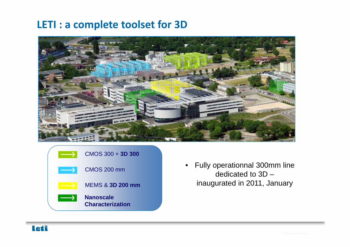
MEMS & 3D 200 mm
CMOS 200 mm
CMOS 300 + 3D 300
Nanoscale Characterization
LETI : a complete toolset for 3D
• Fully operationnal 300mm line dedicated to 3D –
inaugurated in 2011, January

© CEA. All rights reserved
TSV applications
Where do we stand ?
What challenges & perspectives for digital
applications
Pour modifier: Insertion / En Tête/Pied de page
- Titre de la présentation | Auteur| 7

© CEA. All rights reserved
A whole set of applications
Yole Development, 2011
© CEA. All rights reserved
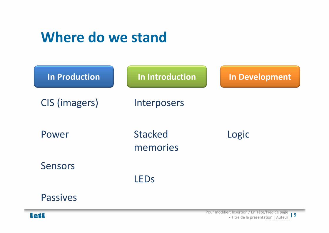
Where do we stand
CIS (imagers)
Power
Sensors
Passives
Pour modifier: Insertion / En Tête/Pied de page
- Titre de la présentation | Auteur| 9
In Production In Introduction In Development
Interposers
Stacked
memories
LEDs
Logic
© CEA. All rights reserved
Qualcomm
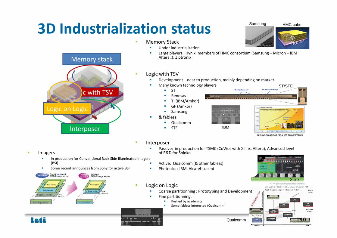
3D Industrialization status
| 10
Memory Stack Under industrialization
Large players : Hynix; members of HMC consortium (Samsung – Micron – IBM Altera..); Ziptronix
Logic with TSV Development – near to production, mainly depending on market
Many known technology players
ST
Renesas
TI (IBM/Amkor)
GF (Amkor)
Samsung
& fabless Qualcomm
STE
Interposer Passive: in production for TSMC (CoWos with Xilinx, Altera), Advanced level
of R&D for Shinko
Active: Qualcomm (& other fabless)
Photonics : IBM, Alcatel-Lucent
Logic on Logic Coarse partitionning : Prototyping and Development
Fine partitionning : Pushed by academics
Some fabless interested (Qualcomm)
Memory stack
Logic with TSV
Interposer
Logic on Logic
Samsung HMC cube
ST/STE
IBM
Xilinx
Imagers In production for Conventional Back Side Illuminated Imagers
(BSI)
Some recent announces from Sony for active BSI

© CEA. All rights reserved
Interposers
An important sector :
As a market
As a first introduction of digital « non-2D » architectures
As a first return on invests
With markets of various size to serve
Pour modifier: Insertion / En Tête/Pied de page
- Titre de la présentation | Auteur| 11
© CEA. All rights reserved
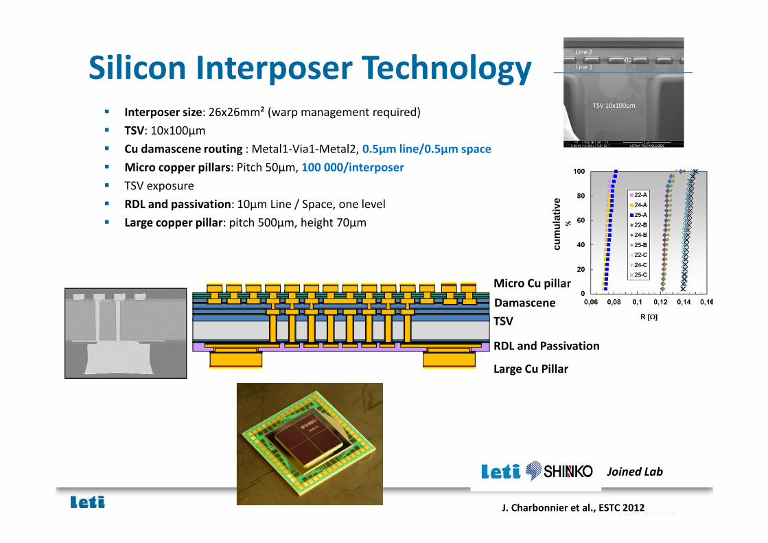
Silicon Interposer Technology Interposer size: 26x26mm² (warp management required)
TSV: 10x100µm
Cu damascene routing : Metal1-Via1-Metal2, 0.5µm line/0.5µm space
Micro copper pillars: Pitch 50µm, 100 000/interposer
TSV exposure
RDL and passivation: 10µm Line / Space, one level
Large copper pillar: pitch 500µm, height 70µm
Large Cu Pillar
TSV
RDL and Passivation
Damascene
Micro Cu pillar
J. Charbonnier et al., ESTC 2012
Joined Lab
cum
ulat
ive

© CEA. All rights reserved
Interposers are not just wires
Pour modifier: Insertion / En Tête/Pied de page
- Titre de la présentation | Auteur| 13
© CEA. All rights reserved
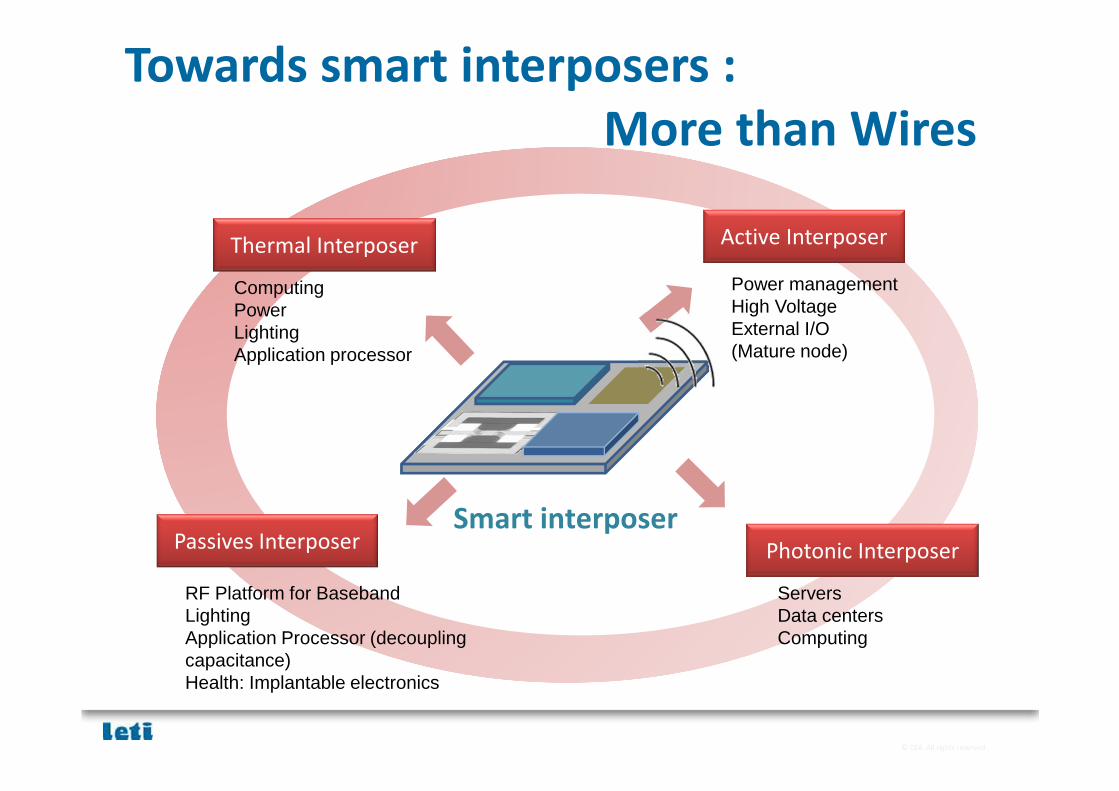
Towards smart interposers :
More than Wires
Passives Interposer
Thermal Interposer
Photonic Interposer
Active Interposer
RF Platform for BasebandLightingApplication Processor (decoupling capacitance)Health: Implantable electronics
ComputingPowerLightingApplication processor
Power managementHigh VoltageExternal I/O(Mature node)
ServersData centersComputing
Smart interposer

© CEA. All rights reserved
Active Interposer Concept
SDRAMMulti-core SoC
Multi-core SoC Multi-core SoC
Heterogeneous integration rationale: Small dies shorten new process introduction and improve overall yield
Analog design and IOs doesn’t shrink a lot with process technology
Short interconnect improves signal and power integrity
SoC partitioning into several dies, with different technology nodes
Active Interposer:
Analog, interconnect,
memory control and I/O
peripherals
Processing layer:
High performance multi-
core processors
Memory layer:
High bandwidth,
Wide data interface
On LETI roadmap for 2015

© CEA. All rights reserved
Digital applications
A generic trend and expectation :
Power Efficiency
Pour modifier: Insertion / En Tête/Pied de page
- Titre de la présentation | Auteur| 16
PC, Video, GamingMID Segment Servers

© CEA. All rights reserved
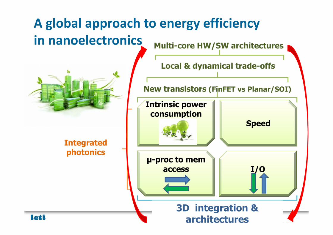
A global approach to energy efficiency
in nanoelectronics
I/O
µ-proc to memaccess
Intrinsic power consumption
Speed
New transistors (FinFET vs Planar/SOI)
Local & dynamical trade-offs
Multi-core HW/SW architectures
Integratedphotonics
3D integration & architectures
© CEA. All rights reserved
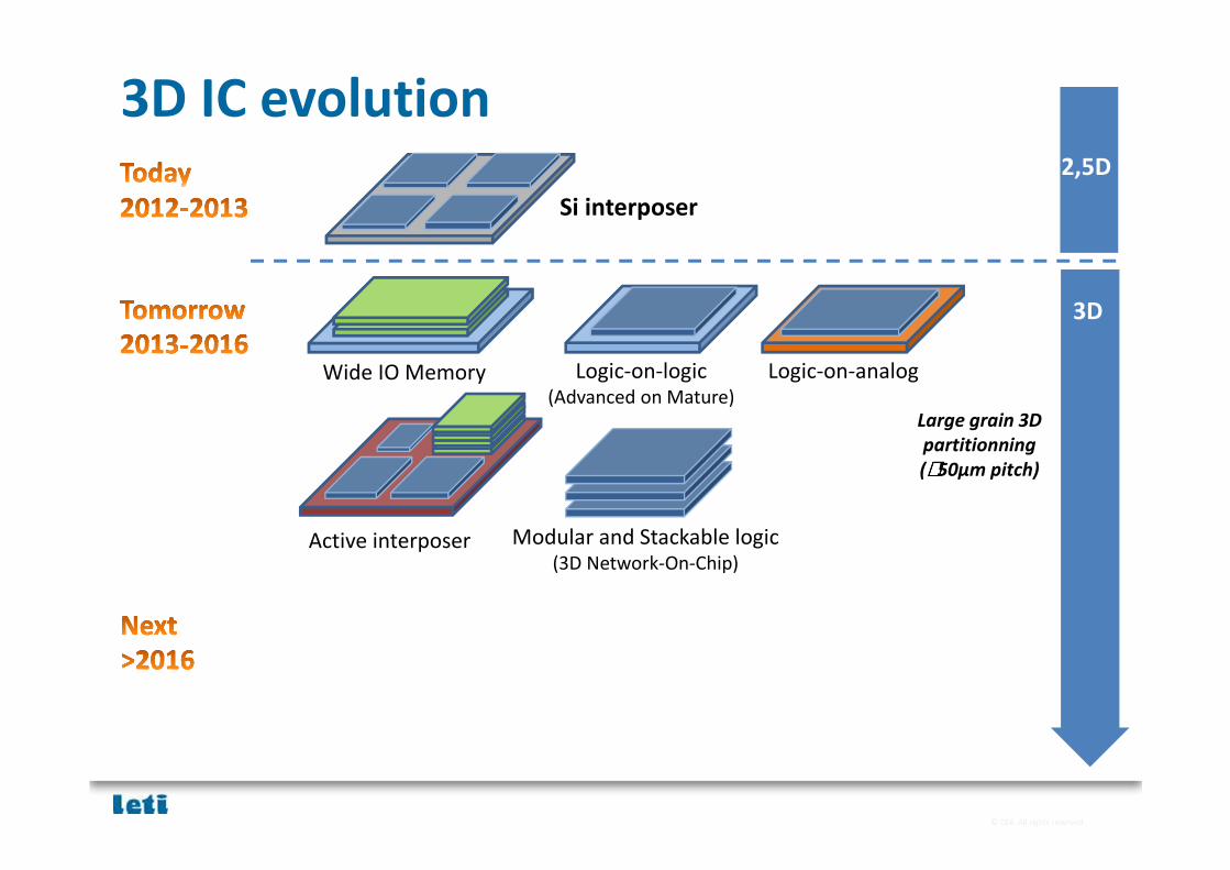
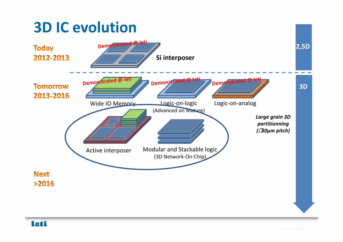
Wide IO Memory Logic-on-analogLogic-on-logic (Advanced on Mature)
Active interposer Modular and Stackable logic(3D Network-On-Chip)
2,5D
3D
Si interposer
3D IC evolution
Large grain 3D
partitionning
(∼∼∼∼50µm pitch)

© CEA. All rights reserved
© CEA. All rights reserved
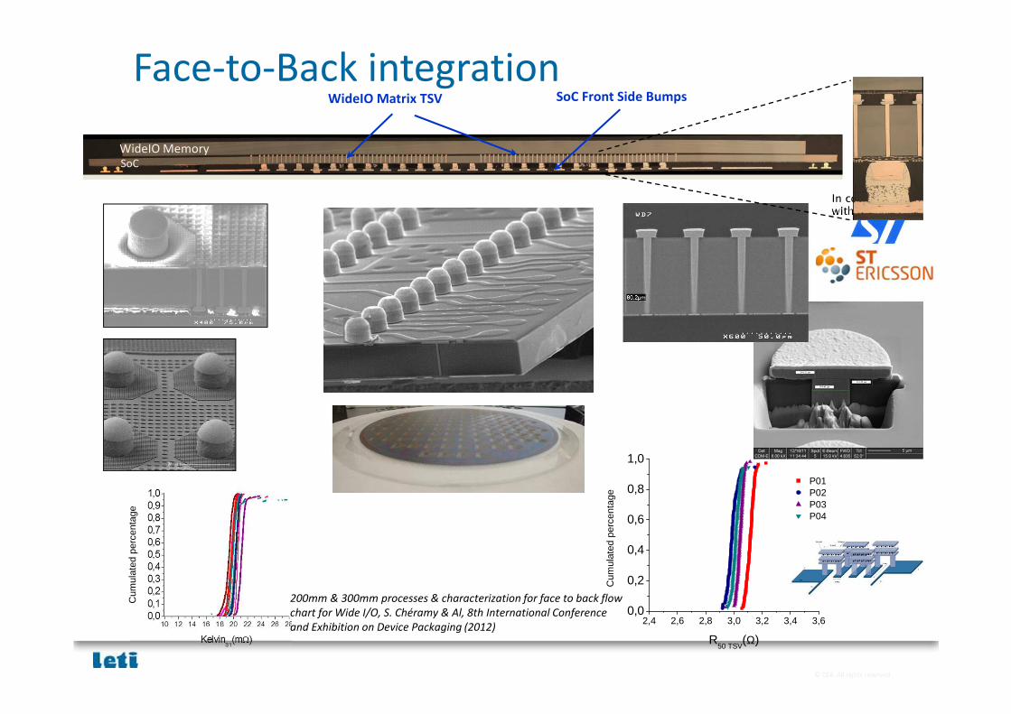
Face-to-Back integration
Cum
ulat
ed p
erce
ntag
e
2,4 2,6 2,8 3,0 3,2 3,4 3,60,0
0,2
0,4
0,6
0,8
1,0
pour
cent
age
cum
ulé
R50 TSV
(Ω)
P01P02P03P04
Cum
ulat
ed p
erce
ntag
e
In collaboration
with
200mm & 300mm processes & characterization for face to back flow
chart for Wide I/O, S. Chéramy & Al, 8th International Conference
and Exhibition on Device Packaging (2012)
WideIO Matrix TSV SoC Front Side Bumps
SoC
WideIO Memory

© CEA. All rights reserved
Face-to-Face Integration for
logic/analog partitioning (65nm technology stacked on 65nm)
TSV
Top / bottom dies
connection
Bottom die / BGA
connection
Cu RDL
Cu TSV
BEOL
Cu TSV
BGA
© CEA. All rights reserved
Wide IO Memory Logic-on-analogLogic-on-logic (Advanced on Mature)
Active interposer Modular and Stackable logic(3D Network-On-Chip)
2,5D
3D
Si interposer
3D IC evolution
Large grain 3D
partitionning
(∼∼∼∼50µm pitch)
© CEA. All rights reserved
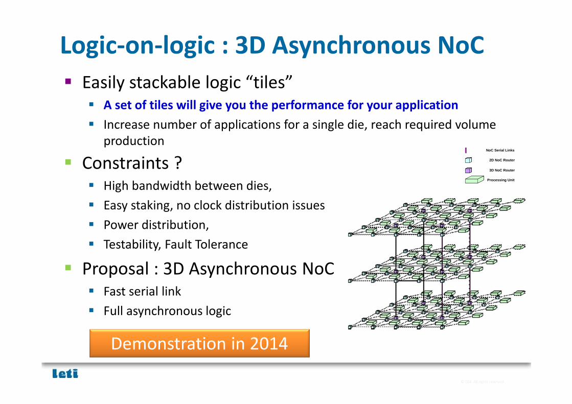
Logic-on-logic : 3D Asynchronous NoC
Constraints ? High bandwidth between dies,
Easy staking, no clock distribution issues
Power distribution,
Testability, Fault Tolerance
Proposal : 3D Asynchronous NoC Fast serial link
Full asynchronous logic
2D NoC Router
3D NoC Router
Processing Unit
NoC Serial Links
Demonstration in 2014
Easily stackable logic “tiles” A set of tiles will give you the performance for your application
Increase number of applications for a single die, reach required volume
production

© CEA. All rights reserved
Wide IO Memory Logic-on-analogLogic-on-logic (Advanced on Mature)
Active interposer Modular and Stackable logic(3D Network-On-Chip)
2,5D
3D
Si interposer
3D IC evolution
Fine grain 3D
partitionning
(∼∼∼∼10µm pitch)
3D Cache memory on
manycore processor
Large grain 3D
partitionning
(∼∼∼∼50µm pitch)

© CEA. All rights reserved
3D Cache Memory on manycore Non-uniform Memory Architecture (NUMA) : splitting uniform cache into
multiple banks interconnected with a NOC
3D stacking adding flexibility, high capacity and a gain on power consumption
High bandwidth and fault tolerance
Eric Guthmuller et al., “Adaptive Stackable 3D
Cache Architecture for Manycores”, ISVLSI2012
1Oµm TSV pitch required
>10000 TSVs per chip
© CEA. All rights reserved
| 26
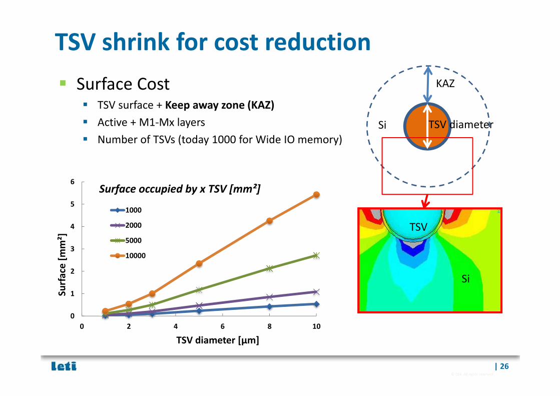
TSV shrink for cost reduction
Surface Cost TSV surface + Keep away zone (KAZ)
Active + M1-Mx layers
Number of TSVs (today 1000 for Wide IO memory)
KAZ
TSV diameter
TSV
Si
Si
0
1
2
3
4
5
6
0 2 4 6 8 10
Su
rfa
ce [
mm
²]
TSV diameter [µm]
Surface occupied by x TSV [mm²]
1000
2000
5000
10000

© CEA. All rights reserved
Low diameter TSV
Reducing Si thickness : 15µm
High Density TSV’s demosntrated in 65nm MOSFETS
3µm
M1
M5
15µm15µm
Investigation on TSV impact on 65nm CMOS devices an d circuitsH. Chaabouni, M. Rousseau, P. Leduc et al., IEDM 2010
© CEA. All rights reserved
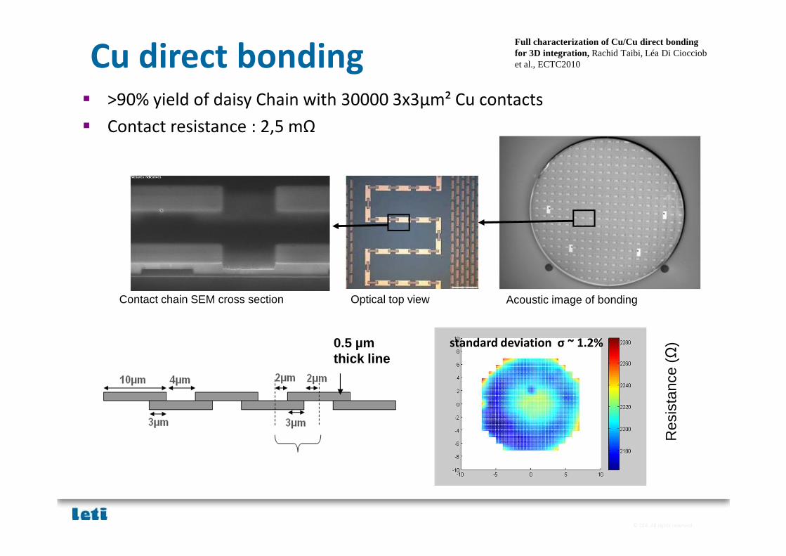
Acoustic image of bonding
0.5 µm thick line
>90% yield of daisy Chain with 30000 3x3µm² Cu contacts
Contact resistance : 2,5 mΩ
Cu direct bonding
Contact chain SEM cross section
Res
ista
nce
(Ω)
Full characterization of Cu/Cu direct bonding for 3D integration, Rachid Taibi, Léa Di Ciocciob et al., ECTC2010
standard deviation σ ~ 1.2%
Optical top view
© CEA. All rights reserved
A global approach to energy efficiency
in nanoelectronics
I/O
µ-proc to memaccess
Intrinsic power consumption
Speed
New transistors (FinFET vs Planar/SOI)
Local & dynamical trade-offs
Multi-core HW/SW architectures
Integratedphotonics
3D integration & architectures
© CEA. All rights reserved
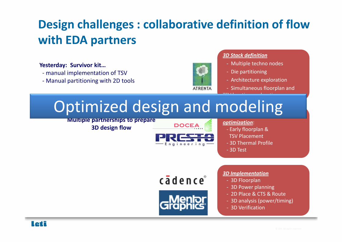
Design challenges : collaborative definition of flow
with EDA partners3D Stack definition
- Multiple techno nodes
- Die partitioning
- Architecture exploration
- Simultaneous floorplan and
TSV location exploration
3D Stack/Package analysis &
optimization:
- Early floorplan &
TSV Placement
- 3D Thermal Profile
- 3D Test
3D Implementation
- 3D Floorplan
- 3D Power planning
- 2D Place & CTS & Route
- 3D analysis (power/timing)
- 3D Verification
Yesterday: Survivor kit…
- manual implementation of TSV
- Manual partitioning with 2D tools
Multiple partnerships to prepare
3D design flow
Optimized design and modeling
© CEA. All rights reserved
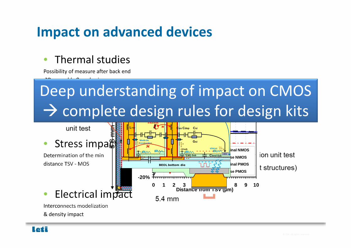
Impact on advanced devices
• Thermal studiesPossibility of measure after back end
3D assembly & packaging
• Stress impactDetermination of the min
distance TSV - MOS
• Electrical impactInterconnects modelization
& density impact
-20%
-15%
-10%
-5%
0%
5%
10%
15%
20%
0 1 2 3 4 5 6 7 8 9 10Distance from TSV (µm)
Mob
ility
var
iatio
n (%
)
Longitudinal NMOS
Transverse NMOS
Longitudinal PMOS
Transverse PMOS
TSV Radius in <110> direction
BEOL bottom die
BEOL top die
MOS
Lcupi +LCupB
Rcupi +RCupB
LTSV
RTSV Vsub
Vsub
Cox Cdep Csi
Cbeol-SubCM1-Sub
Gsi
Custress
Mode de conduction
IFoucauts
MMMM
MMMM
- - - - - -
+ + + + +
amincissement
Deep understanding of impact on CMOS
complete design rules for design kits
© CEA. All rights reserved
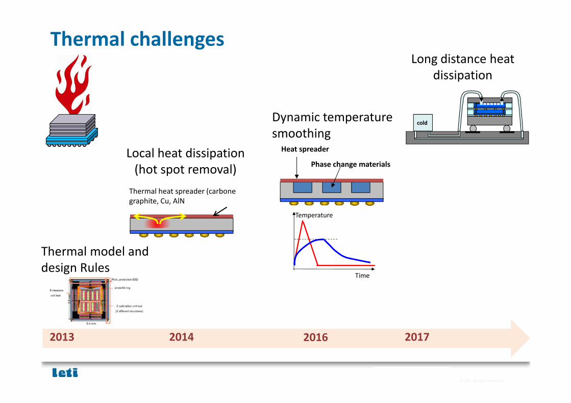
Thermal challenges
Thermal model and
design Rules
Local heat dissipation
(hot spot removal)Phase change materials
Dynamic temperature
smoothingcold
Long distance heat
dissipation
Heat spreader
2013 2014 2016 2017
Thermal heat spreader (carbone
graphite, Cu, AlN
Temperature
Time
© CEA. All rights reserved
Conclusions
• TSV and 3D have (and will have) a global impact
• Applications in Digital require a global approach
• Leti develops 3D globally:• A generic toolbox available (technology & design)
• Capability to transform 3D concepts into silicon demonstrators
• A roadmap of developments and demonstrators
Generic R&D run in open innovation model
Specific developments and prototyping through proprietary
cooperation
© CEA. All rights reserved
Thank you for
your attention
and questions