Trasperant electronics26&18
21
-
Upload
adithya-amara -
Category
Education
-
view
39 -
download
1
Transcript of Trasperant electronics26&18


CONTENTS• Introduction
• Definition
• What are Conductive and Transparent materials?
• Technologies used
• Explanation
• Fabrication of Epitaxial films
• Manufacturing
• Combining Optical Transparency and Electrical conductivity
• Advancements in Technology
• Advantages
• Applications
• Solar windows
• Types of OLEDs
• Future Gadgets
• Conclusion

INTRODUCTION
Transparent Electronics is an
emerging science and
technology which aims to
produce invisible electronic
circuits and optoelectronic
devices
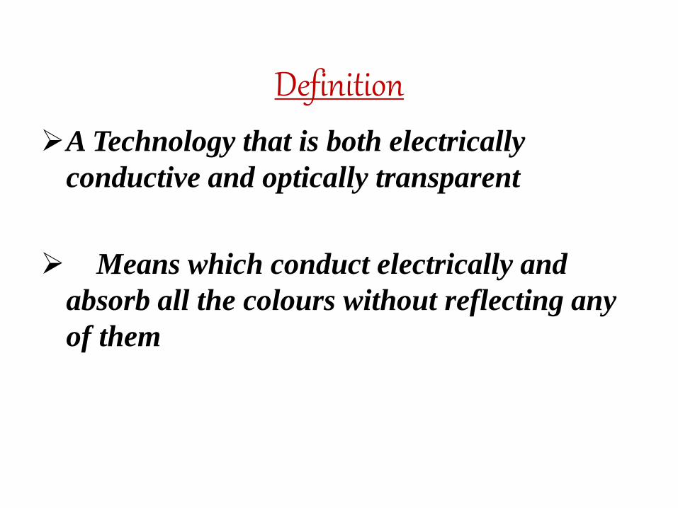
Definition
A Technology that is both electrically
conductive and optically transparent
Means which conduct electrically and
absorb all the colours without reflecting any
of them

CONDUCTIVE AND TRANSPARENT
Conductive material
A conductive material has fermi level of completely filled valance
band and conduction band
Transparent material
A transparent material is an insulator which posses completely
filled valance band and empty conduction band

TECHNOLOGIES USED
• Mainly two technologies are used
• Transparent Conducting Oxide (TCO)
• Transparent Thin Film Transistor (TTFT)

EXPLANATIONTRANSPARENT CONDUCTING OXIDE
Oxides like ZnO , SnOInSnO , In2O3 , SnO2 , CdO used
in achieving optical Transparency along with Electrical
conductivity,employs at low and room temperature.
TRANSPARENT THIN FILM TRANSISTOR
A special kind of FET made by depositing thin films of
semiconductor active layer , dielectric layer and metallic contacts
over a supporting substrate(Glass). It provides high voltage gain
, heat dissipation , radiation tolerances over semiconductor based
TFTs.
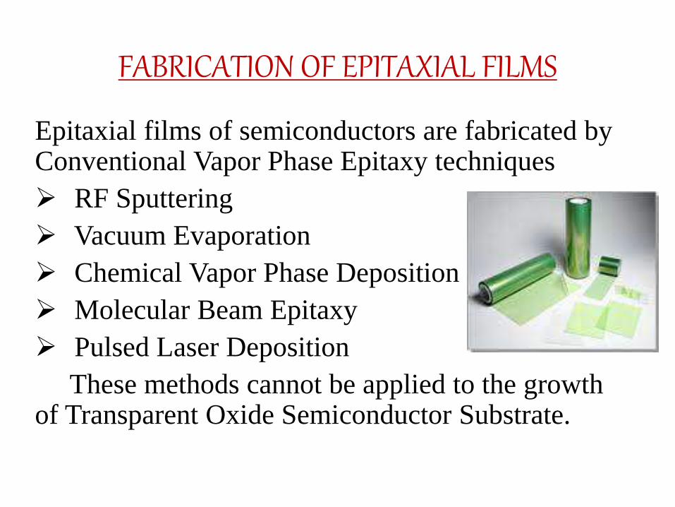
FABRICATION OF EPITAXIAL FILMS
Epitaxial films of semiconductors are fabricated by Conventional Vapor Phase Epitaxy techniques
RF Sputtering
Vacuum Evaporation
Chemical Vapor Phase Deposition
Molecular Beam Epitaxy
Pulsed Laser Deposition
These methods cannot be applied to the growth of Transparent Oxide Semiconductor Substrate.

Fig. RF Sputtering Fig. Vacuum Evaporation
Fig. Molecular Beam Epitaxy Fig. Pulsed Laser Deposition
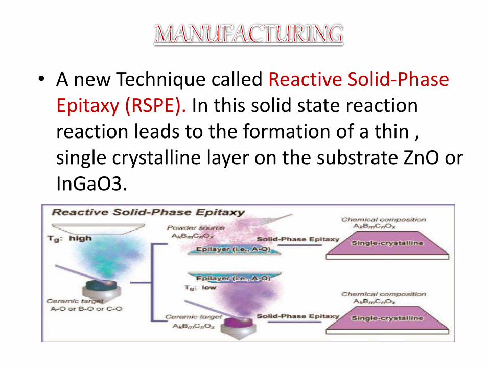
• A new Technique called Reactive Solid-Phase Epitaxy (RSPE). In this solid state reaction reaction leads to the formation of a thin , single crystalline layer on the substrate ZnO or InGaO3.

COMBINING OPTICAL TRANSPARENCY WITH ELECTRICAL CONDUCTIVITY
• To become Transparent Conducting Oxide(TCO) these aredoped with some oxides In2O3,SnO2,ZnO , CdO to displacethe fermi level up into the conduction band which provides
1.The high mobility of extracarriers due to theirsmall effective mass.
2.Low optical absorption dueto the low density of statesin the conduction band.

ADVANCEMENTS IN TECHNOLOGY
• TRRAM (Transparent Resistive RAM)
• provides non-volatile memory means data don’t lost when power off and provides a transmittance of 81% in the visible region.
• ReRAM (memristor)
• It significantly stores more memory and demand less energy and space to
store data. Whose electrical resistance changes when voltage is applied.

ADVANTAGES
• Robust Design
• Viewing Angles
• Stability
• Ease of Production
• Economical
• Environment Friendly
• Electronic Paper


• The Smart Solar Window, which is basically a
window capable of harnessing the power of the
sun and turning it into precious energy for your
electronics and gadgets.

TYPES OF OLEDs
• Transparent OLED
• Top emitting OLED
• Foldable OLED
• White OLED
• Active matrix OLED
• Passive matrix OLED

FUTURE GADGETS

CONCLUSION
• Great impact on human machine interaction
• Lead to new applications
• Cause environmental challenges as currently using IC device

REFERENCES
1. Hiromichi OTHA journal of ceramic society Japan
2. Transparent electronics: from synthesis to applications Wiley publications: Antonio Facchetti, Tobin J. Marks.
3.“Transparent solar cells." PHYSorg.com. 2 Jun 2009.
http://phys.org/news163180542.html