Basic Building Blocks - drshoabkhan.com Design Options for Basic... · Basic Building Blocks...
133
Basic Building Blocks Lecture 5 Dr. Shoab A. Khan
Transcript of Basic Building Blocks - drshoabkhan.com Design Options for Basic... · Basic Building Blocks...

Basic Building Blocks
Lecture 5
Dr. Shoab A. Khan

Embedded Units in FPGAs
New Trends in FPGAs’ Architecture

Digital Design of Signal Processing Systems, John Wiley & Sons by Dr. Shoab A. Khan 3
Embedding in FPGAs
FPGA with PowerPC, MicroBlaze, Ethernet MAC and
other embedded interfaces
Ethernet
MACRJ45
SDRAM
controllerSDRAM
MicroBlaze
Power PCExternal
Memory
Controller
OPB
OPB
PLB
GPIO
UART
Arbiter
address
data
controlFor FPGA
bit-stream
Flash Memory
For program
of CPU

Digital Design of Signal Processing Systems, John Wiley & Sons by Dr. Shoab A. Khan
Embedded Arithmetic Units in FPGAs
4

Digital Design of Signal Processing Systems, John Wiley & Sons by Dr. Shoab A. Khan 5
(a) DSP48 in VirtexTM-4 FPGA (Derived from Xilinx documentation)
A 18
18
18
BCOUT
B
X
48C
4848
48
CIN
72
3838
38 Y48
48X
P
48
+
48
SUBSTRACT
PCOUT
48
Wire shift Right by 17 Bits
A 18
18B
4848
BCOUNT
18
18
18
18
4848
48
CIN
72
3838
38 Y48
48X
P
48
+
48
SUBSTRACT
PCOUT
48
18
18
BCINWire shift Right by 17 Bits
BCIN PCIN
48
PCIN
48
x
x
X

Digital Design of Signal Processing Systems, John Wiley & Sons by Dr. Shoab A. Khan 6
(b)18x18 multiplier and adder in Altera FPGA
DATA-1
BUFFER
COEFFICIENT 1
BUFFER
DATA 2
BUFFER
DATA-3
BUFFER
X
X
X
X
ADDER
ADDER
SUMMATION
UNIT
ADD-
ACCUMULATE
CIRCUIT
37
36
36
36
36
18
18
18
18
18
18
18
18
DATA-4
BUFFER
COEFFICIENT-4
BUFFER
COEFFICIENT-2
BUFFER
COEFFICIENT-3
BUFFER

Digital Design of Signal Processing Systems, John Wiley & Sons by Dr. Shoab A. Khan 7
8x8 multiplier and 16-bit adder in Quick Logic FPGA
INSTRUCTION FIFOs RAM
ADD REGISTER MULTIPLY
BBUS
ABUS
RBUS
CBUS
16
16
8 8
1616
17
3

Digital Design of Signal Processing Systems, John Wiley & Sons by Dr. Shoab A. Khan 8
18x18 multiplier in Virtex-II, Virtex-II pro and
SpartanTM-3 FPGA
18 x18 bit
multiplier
3618
18
A
B

Digital Design of Signal Processing Systems, John Wiley & Sons by Dr. Shoab A. Khan 9
Instantiation of Embedded Blocks
ISE-provided template
// MULT18X18: 18 x 18 signed asynchronous multiplier
// Virtex-II/II-Pro, Spartan-3
// Xilinx HDL Language Template, version 9.1i
MULT18X18 MULT18X18_inst (
.P(P), // 36-bit multiplier output
.A(A), // 18-bit multiplier input
.B(B) // 18-bit multiplier input);
// End of MULT18X18_inst instantiation

Digital Design of Signal Processing Systems, John Wiley & Sons by Dr. Shoab A. Khan 10
Embedded Multipliers
Automatic instantiation
][]2[]1[][ 21 nxnwanwanw
]2[]1[][][ 210 nwbnwbnwbny

Digital Design of Signal Processing Systems, John Wiley & Sons by Dr. Shoab A. Khan 11
+
+
x
x
x
+
+x
x
x[n]
w[n]
w[n]
a1
a2
b0
b1
b2
y[n]
16 32
32
32
16
16
16
16
32
32
32
32
w[n-1]
w[n-2]
16Q
Block diagram of a 2nd Order IIR filter in Direct Form II Realization
(a)

Digital Design of Signal Processing Systems, John Wiley & Sons by Dr. Shoab A. Khan
RTL schematic generated by Xilinx’s Integrated
Software Environment
12
(b)

Digital Design of Signal Processing Systems, John Wiley & Sons by Dr. Shoab A. Khan
Synthesis of the design on Spartan™-3 FPGA, the multiplication and addition
operations are mapped on DSP48 Multiply Accumulate (MAC) embedded
blocks
13
Selected Device : 3s400pq208-5
Minimum period: 10.917ns (Maximum Frequency: 91.597MHz)
Number of Slices: 58 out of 3584 1%
Number of Slice Flip Flops: 32 out of 7168 0%
Number of 4 input LUTs: 109 out of 7168 1%
Number of IOs: 50
Number of bonded IOBs: 50 out of 141 35%
Number of MULT18X18s: 5 out of 16 31%
Number of GCLKs: 1 out of 8 12%
(c)

Digital Design of Signal Processing Systems, John Wiley & Sons by Dr. Shoab A. Khan
RTL schematic generated by Xilinx ISE for Virtex™ 4 target device .
The multiplication and addition operations are mapped on DSP48
multiply accumulate (MAC) embeded blocks
14
(d)

Digital Design of Signal Processing Systems, John Wiley & Sons by Dr. Shoab A. Khan 15
module iir(xn, clk, rst, yn);
// x[n] is in Q1.15 formatinput signed [15:0] xn;input clk, rst;
// y[n] is in Q2.30 formatoutput signed [31:0] yn;
// Full precision w[n] in Q2.30 formatwire signed [31:0] wfn;
// Quantized w[n] in Q1.15 formatwire signed [15:0] wn;
// w[n-1]and w[n-2] in Q1.15 formatreg signed [15:0] wn_1, wn_2;
// all the coefficients are in Q1.15 formatwire signed [15:0] b0 = 16'ha7b0;wire signed [15:0] b1 = 16'hf2b2;wire signed [15:0] b2 = 16'h7610;wire signed [15:0] a1 = 16'h5720;wire signed [15:0] a2 = 16'h1270;

Digital Design of Signal Processing Systems, John Wiley & Sons by Dr. Shoab A. Khan 16
// w[n] in Q2.30 format with one redundant sign bitassign wfn = wn_1*a1+wn_2*a2;
/* through away redundant sign bit and keeping16 MSB and adding x[n] to get w[n] in Q1.15 format */
assign wn = wfn[30:15]+xn;
// computing y[n] in Q2.30 format with one redundant sign bitassign yn = b0*wn + b1*wn_1 + b2*wn_2;
always @(posedge clk or posedge rst)begin
if(rst)begin
wn_1 <= 0;wn_2 <=0;
endelsebegin
wn_1 <= wn;wn_2 <= wn_1;
endEnd
Endmodule

Digital Design of Signal Processing Systems, John Wiley & Sons by Dr. Shoab A. Khan
An 8-tap Direct Form (DF)-I FIR filter
17
x x
+
x
+
x
+ +
x
+
x
+
x
+
y[n]
16 16
x[2]x[0] x[5]x[3] x[4] x[6]
1640
data_out
clk
b0
x[1]
b1 b3 b4 b5 b6 b7
data_in
b2
x[7]
Q16
x

Digital Design of Signal Processing Systems, John Wiley & Sons by Dr. Shoab A. Khan
Example of Optimized Mapping
18
// -------------------------------------------------------------
// Module: fir_filter
// -------------------------------------------------------------
// -------------------------------------------------------------
// Discrete-Time FIR Filter
// -------------------------------
// Filter Structure : Direct-Form FIR
// Filter Order : 7
//
// Input Format: Q1.15
// Output Format: Q1.15
// -------------------------------------------------------------
module fir_filter (
input clk,
input signed [15:0] data_in, //Q1.15
output reg signed [15:0] data_out //Q1.15
);

Digital Design of Signal Processing Systems, John Wiley & Sons by Dr. Shoab A. Khan
Contd…
19
// Constants, filter is designed using Matlab FDATool, all coeffs are in Q1.15 format
parameter signed [15:0] b0 = 16'b1101110110111011;
parameter signed [15:0] b1 = 16'b1110101010001110;
parameter signed [15:0] b2 = 16'b0011001111011011;
parameter signed [15:0] b3 = 16'b0110100000001000;
parameter signed [15:0] b4 = 16'b0110100000001000;
parameter signed [15:0] b5 = 16'b0011001111011011;
parameter signed [15:0] b6 = 16'b1110101010001110;
parameter signed [15:0] b7 = 16'b1101110110111011;
reg signed [15:0] xn [0:7]; // input sample delay line
wire signed [39:0] yn; // Q8.32
// Block Statements
always @(posedge clk)
Begin
xn[0] <= data_in;
xn[1] <= xn[0];
xn[2] <= xn[1];
xn[3] <= xn[2];
xn[4] <= xn[3];

Digital Design of Signal Processing Systems, John Wiley & Sons by Dr. Shoab A. Khan
Contd…
20
xn[5] <= xn[4];xn[6] <= xn[5];xn[7] <= xn[6];data_out <= yn[30:15]; // bring the output back in Q1.15 format
end
assign yn = xn[0] * b0 + xn[1] * b1 + xn[2] * b2 +xn[3] * b3 + xn[4] * b4 + xn[5] * b5 +xn[6] * b6 + xn[7] * b7;
endmodule // fir_filter

Digital Design of Signal Processing Systems, John Wiley & Sons by Dr. Shoab A. Khan
Synthesis reports: (a) ) Eight 18 18-bit embedded multipliers and seven
adders from generic logic blocks are used on a Spartan™-3 family of FPGA
21
Selected device : 3s200pq208-5
Minimum period: 23.290 ns
(Maximum frequency: 42.936 MHz)
Number of slices: 185 out of 1920 9%
Number of Slice Flip Flops: 144 out of 3840 3%
Number of 4 input LUTs: 217 out of 3840 5%
Number of IOs: 33
Number of bonded IOBs: 33 out of 141 23%
Number of MULT18X18s: 8 out of 12 66%
Number of GCLKs: 1 out of 8 12%
(a)

Digital Design of Signal Processing Systems, John Wiley & Sons by Dr. Shoab A. Khan
(b) Eight DSP48 embedded blocks are used once mapped on a Vertix-4 family of
FPGA
22
Selected device : 4vlx15sf363-12
Minimum period: 16.958 ns
(Maximum frequency: 58.969 MHz)
Number of Slices: 9 out of 6144 0%
Number of Slice Flip Flops: 16 out of 12288 0%
Number of IOs: 33
Number of bonded IOBs: 33 out of 240 13%
Number of GCLKs: 1 out of 32 3%
Number of DSP48s: 8 out of 32 25%
(b)

Digital Design of Signal Processing Systems, John Wiley & Sons by Dr. Shoab A. Khan
Optimized Mapping
23
x[n]
0
b0 b1 b2 b3 b4 b5 b6 b7
y[n]
x[n-2] x[n-4] x[n-6] x[n-8] x[n-12] x[n-14]x[n-10]
x
++ + + + + + +
x x x x x x x

Digital Design of Signal Processing Systems, John Wiley & Sons by Dr. Shoab A. Khan
Optimized Mapping
24
Selected Device : 4vlx15sf363-12
Minimum period: 1.891ns (Maximum Frequency: 528.821MHz)
Number of Slices: 9 out of 6144 0%
Number of Slice Flip
Flops:
16 out of 12288 0%
Number of IOs: 33
Number of bonded IOBs: 33 out of 240 13%
Number of GCLKs: 1 out of 32 3%
Number of DSP48s: 8 out of 32 25%

Digital Design of Signal Processing Systems, John Wiley & Sons by Dr. Shoab A. Khan 25
module fir_filter_pipeline (
input clk;
input signed [15:0] data_in; //Q1.15
output signed [15:0] data_out; //Q1.15
// Constants, filter is designed using Matlab FDATool, all coeffs are in Q1.15 format
parameter signed [15:0] b0 = 16'b1101110110111011;
parameter signed [15:0] b1 = 16'b1110101010001110;
parameter signed [15:0] b2 = 16'b0011001111011011;
parameter signed [15:0] b3 = 16'b0110100000001000;
parameter signed [15:0] b4 = 16'b0110100000001000;
parameter signed [15:0] b5 = 16'b0011001111011011;
parameter signed [15:0] b6 = 16'b1110101010001110;
parameter signed [15:0] b7 = 16'b1101110110111011;
reg signed [15:0] xn [0:13] ; // one stage pipelined input sample delay line
reg signed [32:0] prod [0:7]; // pipeline product registers in Q2.30 format
wire signed [39:0] yn; // Q10.30
reg signed [39:0] mac [0:7]; // pipelined mac registers in Q10.30 format
integer i;
always @( posedge clk)
begin

Digital Design of Signal Processing Systems, John Wiley & Sons by Dr. Shoab A. Khan 26
xn[0] <= data_in;for (i=0; i<13; i=i+1)
xn[i+1]=x[i];data_out <= yn[30:14]; // bring the output back in Q1.15 format
end
always @( posedge clk)beginprod[0] <= xn[0] * b0;prod[1] <= xn[2] * b1;prod[2] <= xn[4] * b2;prod[3] <= xn[6] * b3;prod[4] <= xn[8] * b4;prod[5] <= xn[10] * b5;prod[6] <= xn[12] * b6;prod[7] <= xn[14] * b7;
endalways @(posedge clk)begin
mac[0] <= prod[0];for (i=0; i<7; i=i+1)
mac[i+1] <= mac[i]+prod[i+1];end
assign yn = mac[7];
endmodule // fir_filter

Digital Design of Signal Processing Systems, John Wiley & Sons by Dr. Shoab A. Khan
Carry Chain Logic in FPGAs
27
iiii cpgc 1
iii bap
iii bag

Digital Design of Signal Processing Systems, John Wiley & Sons by Dr. Shoab A. Khan
Fast Carry Logic in Vertix™-II pro FPGA Slice
SOP IN0
SHIFT IN
LUT: A B
G4G3
BA
WG4WG3WG2WG1
ALT DIG G2
PROD
G1
BY
Cout
ORCY
YBMUX
SOPOUT
GYMUX
+
Y= A B Cin+
YB
MULIAND10
XORG
Dual-PortShift-Reg
LUTRAMROM
A4A3A2A1
WG4WG3WG2WG1
WS DI
SHIFTOUT
WSG
WE [2:0]
WE
CLK
WSF
SLICEWE[2:0]
BY
CE
CLK
SR
Shared
between
x & y
Registers
MUXCY
MUXCY
0 1
Cin
CYOG
FFLATCH
D Q
CE
Y
SR REV
DY
CKCE
CLK
SR
Q
DIG
DYMUX
Dedicated Carry logic
1 half-Slice= 1bit-adder
P
0 1
+
28

Digital Design of Signal Processing Systems, John Wiley & Sons by Dr. Shoab A. Khan
Fast Carry Logic
MUXCYO I
LUTFF
O I
LUTFF
MUXCY
COUT
to CIN of S2 of the next CLB
SLICE
S3
CIN
COUT
MUXCYO I
LUTFF
O I
LUTFF
MUXCY
SLICE
S2
COUT
MUXCYO I
LUTFF
O I
LUTFF
MUXCY
COUT
to CIN of S2 of the
next CLB
SLICE S1
CIN
COUTMUXCYO I
LUTFF
O I
LUTFF
MUXCY
SLICE S0
COUT
CIN CIN CLB
(Secondary
Carry Chain)
COUT
to S0 of the next CLB
(Fast Carry
Chain)
29

Digital Design of Signal Processing Systems, John Wiley & Sons by Dr. Shoab A. Khan
Fast Carry Chain
A[63:60]
B[63:60]CLB 15
A[11:8]
B[11:8]CLB 2
A[3:0]
B[3:0]CLB 0
A[7:4]
B[7:4]CLB 1
Y[63:60]
Y[64]
Y[11:8]
Y[7:4]
Y[3:0]
A[63:60]
B[63:60]
Y[63:60]
1 CLB = 4 Slices = 2,4bit adders
CLBs must be in same column
+
30

Digital Design of Signal Processing Systems, John Wiley & Sons by Dr. Shoab A. Khan
Designing Customized Multipliers
Parallel multiplier architecture
31
Digital Design of Signal Processing Systems, John Wiley & Sons by Dr. Shoab A. Khan
Adders
Used in addition, subtraction, multiplication and division
Speed of a signal processing or communication system ASIC
depends heavily on these functional units
32

Digital Design of Signal Processing Systems, John Wiley & Sons by Dr. Shoab A. Khan
module HALF_ADDER(ai, bi, si, cout);
input ai, bi;
output si, cout;
// data flow modeling
assign {cout,si} = ai + bi;
endmodule
Half Adder using Data Flow modeling
33

Digital Design of Signal Processing Systems, John Wiley & Sons by Dr. Shoab A. Khan
Half Adder using Data Flow modeling
34
iii baS
iii baC
Half Adder
ai
biSi
cOut

Digital Design of Signal Processing Systems, John Wiley & Sons by Dr. Shoab A. Khan
Full Adder
Truth Table
x y z C S
0 0 0 0 0
0 0 1 0 1
0 1 0 0 1
0 1 1 1 0
1 0 0 0 1
1 0 1 1 0
1 1 0 1 0
1 1 1 1 1
35

Digital Design of Signal Processing Systems, John Wiley & Sons by Dr. Shoab A. Khan
Full Adder
iiii cbas
iiiiii bacbac 1
36
Half Adder
ai
bi
Si
cOut
Cin
cOutHA1
SiHA1 cOutHA2Half Adder

Digital Design of Signal Processing Systems, John Wiley & Sons by Dr. Shoab A. Khan
Gate-level design options for a full adder
ai
ci
Ci+1
bi
si
Half Adder (HA)HA
ai
ci
Ci+1
bi si
pi
gi
(a) (b)

Digital Design of Signal Processing Systems, John Wiley & Sons by Dr. Shoab A. Khan
Contd ...
Ci+1
0
1
ai
bi
0
1
2
3
0
1
2
3
ci
si
ai
ci
Ci+1
bi si
pi
gi
(c) (d)

Digital Design of Signal Processing Systems, John Wiley & Sons by Dr. Shoab A. Khan
module FULL_ADDER(ai,bi,cin,si,cout);
input ai,bi;
input cin;
output si,cout;
wire SiHA1,CoutHA1,CoutHA2;
HALF_ADDER HA1(ai,bi,SiHA1,CoutHA1); // instance HA1
HALF_ADDER HA2(SiHA1,cin,si,Cout); //instance HA2
Or (cout,CoutHA1,CoutHA2); // using or gate primitive
endmodule
Full Adder: Implementation in Verilog

Digital Design of Signal Processing Systems, John Wiley & Sons by Dr. Shoab A. Khan
Full Adder Using Data Flow Modeling
module FULL_ADDER(ai,bi,cin,si,cout);
input ai,bi;
input cin;
output si,cout;
// through data flow level of abstraction
assign {cout,si} = ai + bi + cin;
endmodule
40

Digital Design of Signal Processing Systems, John Wiley & Sons by Dr. Shoab A. Khan
Full Adder Using Data Flow Modeling
41
module FULL_ADDER(ai,bi,cin,si,cout);
input ai,bi;
input cin;
output si,cout;
// through data flow level of abstraction
assign {cout,si} = ai + bi + cin;
endmodule

Digital Design of Signal Processing Systems, John Wiley & Sons by Dr. Shoab A. Khan
Ripple Carry Adder
42
F AF AF AF AF A
a[5]b[5] a[4]b[4] a[3]b[3] a[2]b[2] a[1]b[1] a[0]b[0]
s[5] s[4] s[3] s[2] s[1] s[0]cin
cout
c[1]c[2]c[3]c[4]c[5]c[6]
overflow
F A

Digital Design of Signal Processing Systems, John Wiley & Sons by Dr. Shoab A. Khan 43
module ripple_carry_adder #(parameter W=16)
(input clk,
input [W-1:0] a, b,
input cin,
output reg [W-1:0] s_r,
output reg cout_r);
wire [W-1:0] s;
wire cout;
reg [W-1:0] a_r, b_r;
reg cin_r;
assign {cout,s} = a_r + b_r + cin_r;
always@(posedge clk)
begin
a_r<=a;
b_r<=b;
cin_r<=cin;
s_r<=s;
cout_r<= cout;
end
endmodule

Digital Design of Signal Processing Systems, John Wiley & Sons by Dr. Shoab A. Khan
Six bit ripple carry adder through data flow modeling
// SIX BIT FULL ADDER ;
module fulladder_6bit(s,cout,a,b,cin);
output cout;
output [5:0] s;
input [5:0] a,b;
input cin;
reg [5:0] s,c;
reg cout;
always@(a or b or cin)
begin
{c[0],s[0]}= a[0] + b[0] + cin;
for(i=1; i<6; i=i+1)
{c[i],s[i]}= a[i] + b[i] + c[i-1]; // through data flow modeling.
cout = c[5];
end
endmodule
RCA: Dataflow modeling
44

Digital Design of Signal Processing Systems, John Wiley & Sons by Dr. Shoab A. Khan45
Important Observation
Do we have to wait for the carry to show up to begin doing useful
work?
We do have to know the carry to get the right answer.
But, it can only take on two values
45

Digital Design of Signal Processing Systems, John Wiley & Sons by Dr. Shoab A. Khan
Non-uniform Group 12-Bit Carry Select Adder
Three partitions of 3-bits, 4-bits, 5-bits are made
The cout of the first block is ready earlier making it faster
in functionality than the uniform group 12- bit carry select
adder
So non-uniform group carry select adder is faster than
the uniform group carry select adder
46

Digital Design of Signal Processing Systems, John Wiley & Sons by Dr. Shoab A. Khan47
Carry Generate and Propagate Logic
1
i i i
i i i
i i i i
i i i
g a b
p a b
c g p c
s c p

Digital Design of Signal Processing Systems, John Wiley & Sons by Dr. Shoab A. Khan48
Group Carry and Group Propagate
1112
0001
cpgc
cpgc
010011
00011
cppgpg
cpgpg
3 2 2 1 2 1 0 2 1 0 0
4 3 3 2 3 2 1 3 2 1 0 3 2 1 0 0
0 3 3 2 3 2 1 3 2 1 0
0 3 2 1 0
4 0 0 0
let
and
we can write
c g p g p p g p p p c
c g p g p p g p p p g p p p p c
G g p g p p g p p p g
P p p p p
c G P c
48

Digital Design of Signal Processing Systems, John Wiley & Sons by Dr. Shoab A. Khan
CLA logic for computing carries in two-Gate delay time
49
c0
p0
g0c1
g0
p1
g1
c0p0p1
c2
c3
c0p0p1p2
g0p1p2g1p2
g2
c0p0p1p2p3
g0p1p2p3
g1
p2
p3
g2
p3
g3
c4
ai
bi
ci
pi
si
gi
(a)
(b)

Digital Design of Signal Processing Systems, John Wiley & Sons by Dr. Shoab A. Khan
A 16-bit carry look-ahead adder using two levels of CLA logic
50CLA10
C0
Carry Look Ahead Logic CLA00
Adder AdderC3 C2 C1
s3 a3 b3 s2 a2 b2 s1 a1 b1 s0 a0 b0
p3 g3 p2 g2 p1 g1
AdderAdderAdder
p0 g0
G0P0
G1P1
C4Adder Adder
C7 C6
s7 a7 b7 s6 a6 b6 s5 a5 b5 s4 a4 b4
p7 g7 p6 g6 p5 g5
AdderAdderAdder
p4 g4
CLA01
C5
G2P2
C8Adder Adder
C11 C10
s11 a11 b11 s10 a10 b10 s9 a9 b9 s8 a8 b8
p11 g11 p10 g10 p9 g9
AdderAdderAdder
p8 g8
CLA02
C9
C8Adder Adder
C15 C14
s15 a15 b15 s14 a14 b14 s13 a13 b13 s12 a12 b12
p15 g15 p14 g14 p13 g13
AdderAdderAdder
p12 g12
CLA03
C13
G3P3

Digital Design of Signal Processing Systems, John Wiley & Sons by Dr. Shoab A. Khan
A 64-bit carry look-ahead adder using three levels of CLA logic
51
c48
CLA20
16-bit carry-
lookahead adder
CLA10
4-bit carry-
lookahead adder
c32 c16 c12 c8 c4 c0
P13 G13 P12 G12 P11 G11P10 G10
P20 G20
P03 G03 P02 G02 P01 G01 P00 G00

Digital Design of Signal Processing Systems, John Wiley & Sons by Dr. Shoab A. Khan
A 12-bit Hybrid Ripple Carry and Carry Look-ahead Adder
52
FA
s11 a11 b11
c11
g11 p11
RFA
s10 a10 b10
c10
g10 p10
RFA
s9 a9 b9
c9
g9 p9
RFA
a8 b8
c8
g8 p8
s8
FA
s7 a7 b7
c7
g7 p7
RFA
s6 a6 b6
c6
g6 p6
RFA
s5 a5 b5
c5
g5 p5
RFA
a4 b4
c4
g4 p4
s4
FA
s3 a3 b3
c3
g3 p3
RFA
s2 a2 b2
c2
g2 p2
RFA
s1 a1 b1
c1
g1 p1
RFA
a0 b0 c0
g0 p0
s0
LOOKAHEAD LOGIC LOOKAHEAD LOGIC LOOKAHEAD LOGIC
c12
g7:4

Digital Design of Signal Processing Systems, John Wiley & Sons by Dr. Shoab A. Khan
Binary Carry Look-ahead Adder (BCLA)
53
)(),(),(),(
: asgiven is operatordot theWhere
),(),(),(
1 to1for
),(),(
as solvedy recursivel becan problem theAnd
____________________________________________
1
),(),...(),(),(),(
1,1111
0
11
0000
0011
iiiiiiiiiii
iii
iiiiii
iiiiiiii
iii
iii
PpGpGPGpgPG
end
cPGc
PGpgPG
N-i
pgPG
Eq
pgpgpgpgPG
and
bap
bag

Digital Design of Signal Processing Systems, John Wiley & Sons by Dr. Shoab A. Khan
Binary carry look-ahead adder Serial Implementation
54
S15 S0
0123456789101112131415
………………………………………………………………………

Digital Design of Signal Processing Systems, John Wiley & Sons by Dr. Shoab A. Khan
module BinaryCarryLookaheadAdder
# (parameter N = 16)
(input [N-1:0] a,b,
input c_in,
output reg [N-1:0] sum,
output reg c_out);
reg [N-1:0] p, g, P, G;
reg [N:0] c;
integer i;
always@(*)
begin
for (i=0;i<N;i=i+1)
begin
//generate all ps and gs
p[i]= a[i] ^ b[i];
g[i]= a[i] & b[i];
end
End
___________________________________________
55
Digital Design of Signal Processing Systems, John Wiley & Sons by Dr. Shoab A. Khan
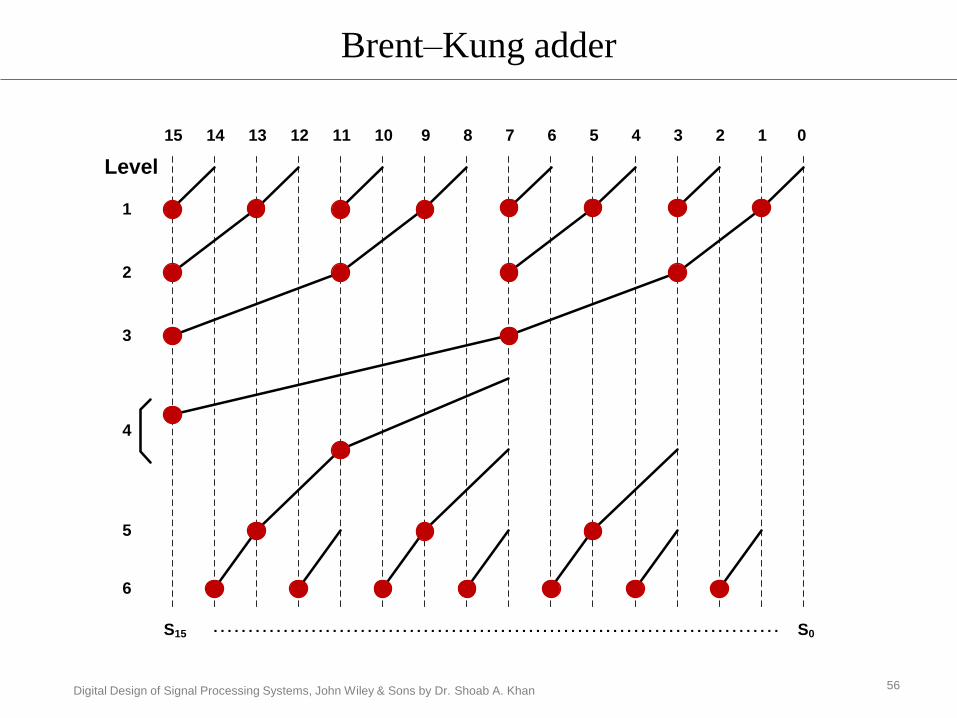
Brent–Kung adder
56
Level
1
2
3
6
4
5
0123456789101112131415
S15 S0………………………………………………………………………

Digital Design of Signal Processing Systems, John Wiley & Sons by Dr. Shoab A. Khan
Ladner–Fischer parallel prefix adder
57
0123456789101112131415
Stage 1
Stage 2
Stage 3
Stage 4
S15………………………………………………………………… S0

Digital Design of Signal Processing Systems, John Wiley & Sons by Dr. Shoab A. Khan
Kogge–Stone parallel prefix adder
58
0123456789101112131415
Stage 1
Stage 2
Stage 3
Stage 4
S15 S0………………………………………………………………………

Digital Design of Signal Processing Systems, John Wiley & Sons by Dr. Shoab A. Khan
Han–Carlson parallel prefix adder
59
0123456789101112131415
Stage 1
Stage 2
Stage 3
Stage 4
Stage 6
S15 S0…………………………………………………………………

Digital Design of Signal Processing Systems, John Wiley & Sons by Dr. Shoab A. Khan
Regular layout of an 8-bit Brent-Kung Adder
60
( g0,p0 )
( g1,p1 )
( g2,p2 )
( g3,p3 )
( g4,p4 )
( g5,p5 )
( g6,p6 )
( g7,p7 )
c3
c2c1 c4
c5
c6
c7

Digital Design of Signal Processing Systems, John Wiley & Sons by Dr. Shoab A. Khan
Carry Skip Adder
If any group generates a carry, it passes it to the next group
In case the group does not generate its own carry then it simply
bypasses the carry from the previous block to its next block
61
1...21 kppppP iiiii
iii bap

Digital Design of Signal Processing Systems, John Wiley & Sons by Dr. Shoab A. Khan
A 16-bit equal-group carry skip adder
4-bit RCA
P[7
:4]
P[0
:3]
4-bit RCA
P[1
5:1
2]
4-bit RCA
P[1
1:8
]
a[3:0] b[3:0]a[7:4] b[7:4]a[11:8] b[11:8]a[15:12] b[15:12]
c_inc_outC4C8C12
OV
4-bit RCA
62

Digital Design of Signal Processing Systems, John Wiley & Sons by Dr. Shoab A. Khan
The process that led to the two-level carry select adder can be continued . . .
A logarithmic time conditional-sum adder results if we proceed to the extreme:
single bit adders at the top
A conditional-sum adder is actually a (log2 k)-level carry-select adder
Implemented in multiple levels
Built using Conditional Cells (CC) and MUX(s)
Conditional Sum Adder
63

Digital Design of Signal Processing Systems, John Wiley & Sons by Dr. Shoab A. Khan
Principle
The conditional cell generates a pair of sum and carry
bits i at each bit position (si0, ci0,si1,ci1)
One pair assumes carry_in of one (si1, ci1) and the other
assumes a carry_in of zero (si0, ci0)
The correct sums and carries are then selected using a
tree of multiplexers
All level one bits are paired up
The sum and carry of the next bit position, brought down
to level 2 are selected by the least significant carry
This continues until all the sums and carries are resolved
in the last level
64

Digital Design of Signal Processing Systems, John Wiley & Sons by Dr. Shoab A. Khan
Example
65
iii
iii
iii
iii
bac
bac
bas
bas
1
0
~1
0

Digital Design of Signal Processing Systems, John Wiley & Sons by Dr. Shoab A. Khan
Conditional Cell (CC)
66
s0i c0i s1i c1i
ai bi

Digital Design of Signal Processing Systems, John Wiley & Sons by Dr. Shoab A. Khan
Addition of three bit numbers using a conditional sum adder
67
(Here we are assuming actual cin=0)
1 1 1
1 0 1
0 1 0
1 0 1
1 0 1
1 1 1
0 1 0
1 1
1 0
1
1 0 0
1
Cin=0
Cin=1
s0i
c0i
s1i
c1i

Digital Design of Signal Processing Systems, John Wiley & Sons by Dr. Shoab A. Khan
Example: Conditional Sum Adder
1
1
1
1
1
0
0
1
1
1
1
0
0
1
0
0
1
0
0
1
0
1
1
0
1
1
0
1
0
0
1
0
0
1
0
1
1
0
1
0
0
1
1
0
1
0
0
0
1
0
1
0
1
0
1
0
0
1
1
0
0
0
1
0
1
1
1
1
0
1
1
1
0
1
0
1
1
0
0
1
0
1
0
1
0
1
1
1
0
1
1
0
0
1
01
1
1100
1
101111
0
00
11
0
01
1
010000
1
10
11
0
000010
11
0
01 110001000010
11
0
67 01234589101112131415
Group sum and block carry out
ai
bi
S0i
C0i
S1i
C1i
ai
bi
i
0
1
0
1
0
1
0
1
0
1
Group
carry-in
Group
width
1
2
4
8
16
01
1
11000111110011
0
11
1
10
1
01
0
00
1
00
1
10
1
11
0
01
1
11
0
00
1
10
0
11
0
11
0
00
1
01
0
68

A 16-bit Conditional Sum Adder
69
S12
S13
S14
S15
C15
S8
S9
S10
S11
S112
S113
S114
S115
C115
S18
S19
S110
S111
S00
CC1Mux
2
CC2
CC3
Mux
2
CC4
CC5
CC7
CC10
CC11
CC13
CC15
CC8
CC9
Mux 2
C1
S1
C02
C11
C05
C7
a0
b0
a1
b1
a2
b2
a3
b3
a4
b4
a5
b5
a6
b6
a7
b7
a8
b8
a9
b9
a10
b10
a11
b11
a12
b12
a13
b13
a14
b14
a15
b15
C00
S01
C01S11
C11
S02
C02S12
C12
S03
C03S13C13
S04
C04S14
C14
S05
C05S15
C15
S06
C06S16
C16
S07
C07S17
C17
S08
C08S18
C18
S09
C09S19
C19
S010
C010S110
C110
S011
C011S111
C111
S012
C012S112
C112
S013
C013S113
C113
S014
C014S114C114
S015
C015S115C115
S02
S03
C03
S12
S13
C13
S2
S3
C3
C04
S05
C05
C14
S15
C15
S06
S07
C07
C06 C16
S04
S05
S06
S07
C07
S4
S5
S6
S7
C7S16S17
C17
C17
C08
S09
C09
C010
C09
S010
S011
C011
C011
S010S011C011
S110
S111
C111
S110
S111
C111
C110
C19
C012S013
C013
S113
C113
C112
C014S014
S015
C015
S114
S115
C115
C114
C114
S012
S013
S014
S015
C015
S112
S113
S114
S115
C115
C111C013
C13
C12
S14
S15
S16
S17
C17
CC0
CC6
CC12
CC14
Mux
3Mux
2
Mux
2
Mux
2
Mux
2
Mux
3
Mux
2
Mux
5
Mux
3
Mux
2C18
S19
C19
Mux
2
Mux
2
Mux
2
Mux
3
Mux
3
Mux
5
Mux
2
Mux
2
Mux
2
Mux
5
Mux
3
Mux
9
Mux
2
Mux
3
S012
S013
S014
S015
C015
S08
S09
S010
S011

Digital Design of Signal Processing Systems, John Wiley & Sons by Dr. Shoab A. Khan
Hybrid Adder Designed
Hybrids are obtained by combining elements of:
Ripple-carry adders
Carry-lookahead (generate-propagate) adders
Carry-skip adders
Carry-select adders
Conditional-sum adders
You can obtain adders with
higher performance
greater cost-effectiveness
lower power consumption
70

Digital Design of Signal Processing Systems, John Wiley & Sons by Dr. Shoab A. Khan
Example
71
iii
iii
iii
iii
bac
bac
bas
bas
1
0
~1
0

Digital Design of Signal Processing Systems, John Wiley & Sons by Dr. Shoab A. Khan
A 16 –bit uniform-groups carry select adder
72
4 bit Ripple
Carry Adder
b[11:8] a[11:8] b[7:4] a[7:4] b[3:0] a[3:0] b[15:12] a[15:12]
0
4 bit 2-to-1 Mux4 bit 2-to-1 Mux 4 bit 2-to-1 Mux 4 bit 2-to-1 MuxC[4]C[8]
S[7:4] S[3:0]S[11:8]S[15:12]
CoutCin
C[12]
C0
C1 4 bit Ripple
Carry Adder
4 bit Ripple
Carry Adder0C0
C1 4 bit Ripple
Carry Adder
4 bit Ripple
Carry Adder0
1
C0
C1 4 bit Ripple
Carry Adder
4 bit Ripple
Carry Adder0C0
C1 4 bit Ripple
Carry Adder1 1 1

Digital Design of Signal Processing Systems, John Wiley & Sons by Dr. Shoab A. Khan
Hierarchical CSA
73
N/4- bit adder
Mux
N/4-bit adder N/4-bit adder N/4-bit adder0 0 0
1 1 1
N/4+1 N/4+1N/4 N/4 N/4N/4+1 N/4+1
CN/4
N/4
N/2+1
01
Cout
bit adderN/4-N/4- bit adderN/4-bit adderCin
43
:1N
Na
43:1 NNb
2:1
43 NNa
4:1
2NNa
2:1
43 NNb
4:12
NNb
0:1
4Nb
0:14Na
2:1
NNs
4:1
2NN
s
0:1
4Ns
CN/2
1 Mux 0 1 Mux 0

Digital Design of Signal Processing Systems, John Wiley & Sons by Dr. Shoab A. Khan
Barrel Shifter
74

Digital Design of Signal Processing Systems, John Wiley & Sons by Dr. Shoab A. Khan
(a) Design of a logic shifter for an 8-bit Operand (b) Design of logic and
arithmetic shifter for an 8-bit signed operand
75
x0
1
2
3
4
5
6
7
8
9
10
11
12
13
14
15
{ x[7], x[7:1] }
{ 2{x[7]}, x[7:2] }
{ 3{x[7]}, x[7:3] }
{ 4{x[7]}, x[7:4] }
{ 5{x[7]}, x[7:5] }
{ 6{x[7]}, x[7:6] }
{ 7{x[7]}, x[7] }
8'b0
{ x[0], 7'b0 }
{ x[1:0], 6'b0 }
{ x[2:0], 5'b0 }
{ x[3:0], 4'b0 }
{ x[4:0], 3'b0 }
{ x[5:0], 2'b0 }
{ x[6:0], 1'b0 }
8
8
8
8
8
8
8
8
8
8
8
8
8
8
8
8
8y
4
1
4
5
6
7
8
9
10
11
12
13
14
15
x[7:1]
x[7:4]
8'b0
{ x[0], 7'b0 }
{ x[1:0], 6'b0 }
{ x[2:0], 5'b0 }
{ x[3:0], 4'b0 }
{ x[4:0], 3'b0 }
{ x[5:0], 2'b0 }
{ x[6:0], 1'b0 }
8
8
8
8
8
8
8
8
8
8
8
8
8
8y
1 1
x[7] 0
L / A
1
7
4
5
6
s
x 8
2x[7:2]
82
0
x[7:3]
38
3
1
x[7:5]
x[7:6]
x[7]
2
3
7
4
5
6
7
6
5
4
3
2
1
4
1 0
(a) (b)

Digital Design of Signal Processing Systems, John Wiley & Sons by Dr. Shoab A. Khan
Design of a Barrel Shifter performing shifts in multiple stages (a)
Single cycle design
76
15
16
31{x[14:0],16'b0}
{15[sgn] },x[15,0]
31x[15:0]
L/A 1 0
23
y1
y1>>4
19
19
y1[18:0]
y1[22:4]
19
y2
y2>>2
17
17
y2[16:0]
y2[18:2]
17
y3
y3>>1
16
16
y3[15:0]
y3[16:1]
16y
31
y0
y0>>8
23
y0[22:0]
y0[30:8]s4
0
1
s3
0
1
s2
0
1
s1
0
1
s0
0
1
23
15 15
{15{x[15]}} 15'b0
(a)

Digital Design of Signal Processing Systems, John Wiley & Sons by Dr. Shoab A. Khan
Design of a Barrel Shifter performing shifts in multiple (b)
Pipelined design
77
16 y
15 15
15'b0{15{x[15]}}
15
16
31{x[14:0],16'b0}
{15[sgn] },x[15,0]
31x[15:0]
L/A 1 0
s4
31
y0
0
1y0>>8
y0[22:0]
y0[30:8]
y0_reg
23
23
y1
23y1>>4
y1[18:0]
y1[22:4]
0
1
y1_reg
19
19y2>>2
y2[16:0]
y2[18:2]
0
1
y2_reg
17
17
s2
y2
19
y3>>1
y3[15:0]
y3[16:1]
0
1
y3_reg
16
16
s1
y3
17
43
21
s-reg
sp_reg spp_regsppp_reg
54
3
0
1
(b)

Digital Design of Signal Processing Systems, John Wiley & Sons by Dr. Shoab A. Khan
Carry Save Adders and Compressors
78

Digital Design of Signal Processing Systems, John Wiley & Sons by Dr. Shoab A. Khan
= 0 0 1 0 1 1
= 0 1 0 1 0 1
= 1 1 1 1 0 1
= 1 0 0 0 1 1= 0 1 1 1 0 1
a0
a1
a2
sc
N+1 N
3:2
NN N
c s
a0 a1 a2
The CSA does not ripple any carry
It has a delay of one FA
The concept of CSA is effective in designing partial products compression/
reduction logic
Carry Save Addition saves the carry at next bit location
79

Digital Design of Signal Processing Systems, John Wiley & Sons by Dr. Shoab A. Khan
Dots are used to represent each bit of the partial product
Dot notation facilitates description of different reduction schemes
Dots are used to represent each bit of the partial product
80
Multiplicand
Multiplier
b[0]
Partial Product pp[0]
b[1]b[2]b[3]
a[0]
Digital Design of Signal Processing Systems, John Wiley & Sons by Dr. Shoab A. Khan
Designing Customized Multipliers
Parallel multiplier architecture
81

Digital Design of Signal Processing Systems, John Wiley & Sons by Dr. Shoab A. Khan
Three components of a multiplier
82
N-bit inputs operands
Partial Product Array Generation = N shifted binary
numbers
Partial Product Array Reduction= reduction to 2 binary
numbers
Final addition = 2N-bit final product

Digital Design of Signal Processing Systems, John Wiley & Sons by Dr. Shoab A. Khan
Three components of a multiplier
multiplicand
multiplier
PP Generation
NN
PP Reduction
CPA
2N
Product
…
83

Digital Design of Signal Processing Systems, John Wiley & Sons by Dr. Shoab A. Khan
Partial Product Generation for a 6x6 Multiplier
84
b5 b0 a5 a0
Multiplicand Multiplier
=
PPij

Digital Design of Signal Processing Systems, John Wiley & Sons by Dr. Shoab A. Khan
Partial Product Generation Verilog Code
85
module multiplier (input [5:0] a,b,output [11:0] prod);
integer i;
reg [5:0] pp [0:5]; // 6 partial products
always@*begin
for(i=0; i<6; i=i+1)begin
pp[i] = b & {6{a[i]}};end
end
assign prod = pp[0]+{pp[1],1'b0}+{pp[2],2'b0}
+{pp[3],3'b0}+{pp[4],4'b0}+{pp[5],5'b0};
endmodule

Digital Design of Signal Processing Systems, John Wiley & Sons by Dr. Shoab A. Khan
Reducing number of dots in a column
86
Level ( n+1)
Level n
sum
carry
sum
carry
(FA) (HA) No operation

Digital Design of Signal Processing Systems, John Wiley & Sons by Dr. Shoab A. Khan 87
Three dots are shown
Each symbolizes a partial product
Using FA reduces these to two bits
One has the weight of 20(sum)
The other has the weight of 21(carry)
This type of reduction is known as 3 to 2 reduction or
carry saves reduction
The two dots are reduced to 2 using a HA

Digital Design of Signal Processing Systems, John Wiley & Sons by Dr. Shoab A. Khan
Partial Products Reduction Schemes
Carry Save Reduction Scheme
Dual Carry Save Reduction Scheme
Wallace Tree Reduction Scheme
Dadda Tree Reduction Scheme
88

Digital Design of Signal Processing Systems, John Wiley & Sons by Dr. Shoab A. Khan
Considers three rows at a time
Take first three rows use CSA to reduce them to two
Iteratively take two layers from previous reduction and a new
from PP layer and reduce them to two using a CSA
Finally produces two layers
Also produces free product bits
The two layers are added using any CPA
12x12 Carry Save Reduction Scheme
89

Digital Design of Signal Processing Systems, John Wiley & Sons by Dr. Shoab A. Khan
PP reduction for a 12x12 Multiplier using Carry Save Reduction Scheme
90
First 3 Partial Products
Level 0
Level 1
Free product bitsFinal partial product
rows that need carry
propagate adder

Digital Design of Signal Processing Systems, John Wiley & Sons by Dr. Shoab A. Khan
Carry Save Reduction Scheme Layout for a 6x6 Multiplier
91
FA FA FA FA
FA
FA FA HA
FA FA FA HA
FA FA FA
HA
P P P 1 2 3 P 4
Free product bits
Level 3
Level 2
Level 1
Level 0
FA
FA
FA
FA
FA
HA
FA
HA
P 0
CPA

Digital Design of Signal Processing Systems, John Wiley & Sons by Dr. Shoab A. Khan
Dual Carry Save Reduction
The partial products are divided into 2 equal size groups
The carry save reduction scheme is applied on both the
groups simultaneously
This results into two partial product layers in each group
The four layers are then reduced using Carry Save
Reduction
The last two layers are added using any CPA
92

Digital Design of Signal Processing Systems, John Wiley & Sons by Dr. Shoab A. Khan
Wallace Tree Multipliers
One of the most commonly used multiplier architecture
It is log time array multiplier
The number of adder levels increases logarithmically as the partial
product rows increase
93

Digital Design of Signal Processing Systems, John Wiley & Sons by Dr. Shoab A. Khan
Wallace Tree Multipliers
Make group of threes and apply CSA reduction in parallel
Each CSA layer produces two rows
These rows then, with other rows from other partial product groups,
form a new reduced matrix
Iteratively apply Wallace reduction on the new generated matrix
This process continues until only two rows are left
The final rows are added together for the final product
94

Digital Design of Signal Processing Systems, John Wiley & Sons by Dr. Shoab A. Khan
Wallace Reduction Tree applied on 12 PPs
95
1510152023
5Level 0
Level 1
Free Product
BitsFinal Partial Product row that need carry
propagate adder
Level 2
Level 3
Level 4
Level 5
10
5
10

Digital Design of Signal Processing Systems, John Wiley & Sons by Dr. Shoab A. Khan
Wallace Reduction layout for a 6x6 array of PPs
96
FAFAFAFA HAHA
FAFA HAFA
HAHAFAFAFAHAHA
P2 P0P1P3PC4PS4PC5PS6PS6PC7PS7PC8PS8PC9PS9PC10PS10PS11 PC6
HA
FAFA
HA
Level 1
Level 2
Level 3
FAFAFAFA HAHA

Digital Design of Signal Processing Systems, John Wiley & Sons by Dr. Shoab A. Khan
Dada Reduction uses the Wallace Reduction Table
Number of partial
Products
Number of full adder
Levels
3 1
4 2
5 n 6 3
7 n 9 4
10 n 13 5
14 n 19 6
20 n 28 7
29 n 42 8
43 n 63 9
Adder Levels in Wallace Tree Reduction Scheme

Digital Design of Signal Processing Systems, John Wiley & Sons by Dr. Shoab A. Khan
Dada Reduction
Minimizes the number of HAs and FAs
Reduction considers each column separately
Reduces the number of dots in each column to the maximum
number of layers in the next level in Wallace Reduction Table
98

Digital Design of Signal Processing Systems, John Wiley & Sons by Dr. Shoab A. Khan
Dadda reduction levels for reducing eight PPs to two
99
Digital Design of Signal Processing Systems, John Wiley & Sons by Dr. Shoab A. Khan
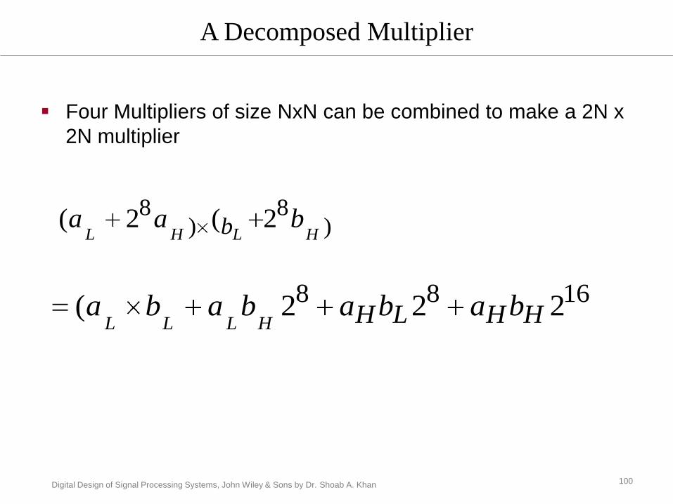
A Decomposed Multiplier
100
Four Multipliers of size NxN can be combined to make a 2N x
2N multiplier
)8
)8 2(2(
HLHLbaa b
1688 222( HHLH babababaHLLL

Digital Design of Signal Processing Systems, John Wiley & Sons by Dr. Shoab A. Khan
A 16x16 bit Multiplier decomposed into four 8x8 multipliers
101
32-Bits
aL X bL 16-Bits
aL X bH 16-Bits
aH X bL 16-Bits
aH X bH 16-Bits

Digital Design of Signal Processing Systems, John Wiley & Sons by Dr. Shoab A. Khan
The results of these multipliers are appropriately added
to get the final product
102
Stage 1
Stage 2
Stage 3
8x8 Multiplier

Digital Design of Signal Processing Systems, John Wiley & Sons by Dr. Shoab A. Khan
Optimized Compressors
103
( 3,2 )
( 3,2 )
c_inc_out
( 3,2 )
( 3,2 )
( 3,2 )
( 3,2 )
( 3,2 )
( 3,2 )
(a)
Candidate implementation of 4:2 compressor
(b)
Concatenation of 4:2 compression to create wider tiles

Digital Design of Signal Processing Systems, John Wiley & Sons by Dr. Shoab A. Khan
Contd…
104
(c)
Use of 4:2 compressor in Wallace tree reduction of
an 8x8 multiplier
(d)
Use of 4:2 compressor in an 88 multiplier in Dadda
reduction

Digital Design of Signal Processing Systems, John Wiley & Sons by Dr. Shoab A. Khan
Single- and Multiple-column Counters
A 6:3 counter reducing six layers of multiple operands to three
A 6:3 counter is mapped on three 6-input LUTs
P5
P4
P3
P2
P1
P0
6-LUT
P5 P4 P3 P2 P1
Carry1 Carry0 Sum
Carry1 Carry0 Sum
x 2i+2
x 2i+1
x 2i
6-LUT 6-LUT
P0
6-bit partial
product x6
6:3 -compressor x6
20
21
22
23
24
25
105

Digital Design of Signal Processing Systems, John Wiley & Sons by Dr. Shoab A. Khan
Counters compressing a 15x15 matrix
15:4, 4:3 and 3:2 counters working in cascade to compress a 15x15 matrix
106
CPA
Co
mp
ressio
n r
atio
15
:4
Co
mp
ressio
n r
atio
4:3
Co
mp
ressio
n r
atio
3:2
CPA

Digital Design of Signal Processing Systems, John Wiley & Sons by Dr. Shoab A. Khan
A (3,4,5:5) GPC compressing three columns with 3, 4,
and 5 bits to 5 bits in different columns
107

Digital Design of Signal Processing Systems, John Wiley & Sons by Dr. Shoab A. Khan
Compressor Tree Synthesis using compression of two
columns of 5 bits each into 4 bit (5, 5; 4) GPCs
Two columns of 5 bits each results into 4-bit
This GPC is represented as (5,5;4)
108

Digital Design of Signal Processing Systems, John Wiley & Sons by Dr. Shoab A. Khan
Compressor tree mapping by (a) 3:2 counters (b) and a (3, 3;
4) GPC
109
(a) (b)

Digital Design of Signal Processing Systems, John Wiley & Sons by Dr. Shoab A. Khan
Two’s Complement Signed Multiplier
The sign bit in 2’s complement representation plays a critical role in
signed multiplier
110
iN
i
iN
n xxx 22
2
0
11
i
i
iN
ni
i
N
bbaiPP 22)2(][
22
2
0
11
for i=0,1,…,N1-2
i
i
iN
nN
N
N
bbaNPP 22)12(]1[
22
2
1
0
111
11

Digital Design of Signal Processing Systems, John Wiley & Sons by Dr. Shoab A. Khan
FGPAs are best suited for counters and GPC-based compression trees
LUTs in many FPGAs come in groups of two with shared 6-bit input
A GPC (3,3;4) best utilize 6-LUT-based FPGAs
61
1
1
1
LUT
LUT
LUT
LUT
111
61
1
1
LUT
LUT
LUT
Not
Used
(a)
An Altera FPGA Adaptive Logic Module (ALM ) contains two
6-LUTs with shared inputs, 6 inputs, 3 outputs GPC has 3/4
logic utilization
(b)
A 6 inputs, 4 outputs GPC has full logic utilization.
Optimized GPC for FPGA Implementation

Digital Design of Signal Processing Systems, John Wiley & Sons by Dr. Shoab A. Khan
Showing 4 x 4-bit signed by signed multiplication
To cater for the sign bit
The sign bits of the first three PPs are extended
Two’s complement of the last PP is taken
HW implementation results in additional logic
1 1 1 1 1 1 0 1
0 0 0 0 0 0 0 X1 1 1 1 0 1 X X
0 0 0 1 1 X X X
0 0 0 0 1 0 0 1
1 1 0 1
1 1 0 1 sign extension logic
112

Digital Design of Signal Processing Systems, John Wiley & Sons by Dr. Shoab A. Khan
Sign - extension Elimination
113
+
B= 0 0 0 0 0 0 . 1 1 0 1 0 1 1B= 1 1 1 1 1 0 . 1 1 0 1 0 1 1
0 0 0 0 0 0 . 1 1 0 1 0 1 1
1
flip the sign bitextend all 1s
add 1 at the location of sign bit
(a)
(b)
+
B= 1 1 1 1 1 1 . 1 1 0 1 0 1 1B= 1 1 1 1 1 1 . 1 1 0 1 0 1 1
1 1 1 1 1 1 . 1 1 0 1 0 1 1
1
flip the sign bitextend all 1s
add 1 at the location of sign bit
Digital Design of Signal Processing Systems, John Wiley & Sons by Dr. Shoab A. Khan
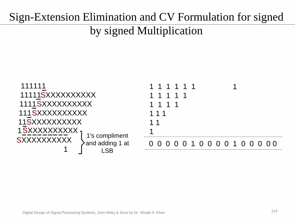
Sign-Extension Elimination and CV Formulation for signed
by signed Multiplication
114
111111
11111SXXXXXXXXXX
1111SXXXXXXXXXX
111SXXXXXXXXXX
11SXXXXXXXXXX1SXXXXXXXXXX
SXXXXXXXXXX
1 1 1 1 1 1
1 1 1 1 1
1 1 1 1
1 1 1
1 1
1
0 0 0 0 0 1 0 0 0 0 1 0 0 0 0 0
1
1's compliment
and adding 1 at
LSB1

Digital Design of Signal Processing Systems, John Wiley & Sons by Dr. Shoab A. Khan
Multiplying two numbers, 0011 and 1101
0 0 1 0
1 1 0 1
1 1 1 1 0 0 1 0
1 1 1 0 0 0 0
1 1 0 0 1 0
1 0 0 1 0
1 1 1 1
Negative Number
1
Correction
Vector
(a)
All the 1s in red area are added to get CV
The CV is 8’b0001_0000

Digital Design of Signal Processing Systems, John Wiley & Sons by Dr. Shoab A. Khan
Contd…
0 0 1 0
1 1 0 1 1 1 0 1 01 0 0 0 X
1 0 1 0 X X0 1 0 1 X X X
1 1 1 1 0 1 0
Correction Vector
(b)
CV is simply added as one of PP
In case of NxN multiplier, CV is always a 1 at N+1 bit location

Digital Design of Signal Processing Systems, John Wiley & Sons by Dr. Shoab A. Khan
Contd…
The MSB of all the PPs except the last one are flipped
and a 1 is added at the sign-bit location, and the number
is extended by all 1s
For the last PP, the two’s complement is computed
Flip all the bits and adding 1 to the LSB position
The MSB of the last PP is flipped again and 1 is added
to this bit location for sign extension.
All these 1s are added to find a correction vector (CV)

Digital Design of Signal Processing Systems, John Wiley & Sons by Dr. Shoab A. Khan
Application of the string property
Hence the number of 1(s) has reduced from 14 to 6. Both have the same
value.
0 0 1 1 1 1 0 1 1 1 1 0 1 1 1 0 101 1
0 0 1 1 1 1 0 1 1 1 1 1 0 0 1 0 101 1
0 0 1 1 1 1 0 0 0 0 0 1 0 0 1 0 111 1
0 0 1 1 1 1 1 0 0 0 0 1 0 0 1 0 110 0
0 1 0 0 0 0 1 0 0 0 0 1 0 0 1 0 110 0
String
String
String
String
118

Digital Design of Signal Processing Systems, John Wiley & Sons by Dr. Shoab A. Khan
Generation of four PPs
119
10 10 11 01
-2 +1 -1 1
11111111 10 10 11 01
00000001 01 00 11
11111010 11 01
00101001 1
00100101 01 00 10 01

Digital Design of Signal Processing Systems, John Wiley & Sons by Dr. Shoab A. Khan
An 8 x 8 bit modified Booth recoder multiplier
120
3
3
3
3
92a
-2a
a0-a
2a0a
-a -2a
16
0
BR0
BR3
BR2
BR1
b6
b7
b4
b5
b2
b3
b0
b1
3-5
3-5
3-5
3-5
Wallace Tree
Reduction
Scheme
CV
16 Bit
CSA
Digital Design of Signal Processing Systems, John Wiley & Sons by Dr. Shoab A. Khan
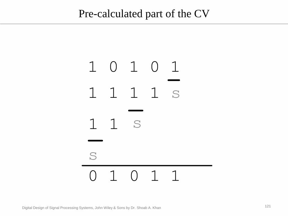
Pre-calculated part of the CV
121
1 0 1 0 1
1 1 1 1
1 1
s
s
s
0 1 0 1 1

Digital Design of Signal Processing Systems, John Wiley & Sons by Dr. Shoab A. Khan
Algorithm Transformations for CSA
122
;1
;0
)21(
;432
;211
sel
else
sel
sumsumif
opopsum
opopsum
)4321())43(21( opopopopsignopopopopsign
To transform the logic for optimal use of compression tree the algorithm is modified as:

Digital Design of Signal Processing Systems, John Wiley & Sons by Dr. Shoab A. Khan
Multiple operands addition should use compression tree
Avoid multiple instantiations of CPA
The example adds Q1.5, Q5.3, Q4.7, and Q6.6 format sign
numbers
Compute CV using sign extension elimination technique
Add it as 5th partial product
Compress using dadda tree
The last two rows can be added using any CPA
Example: Multi Operands addition
123

Digital Design of Signal Processing Systems, John Wiley & Sons by Dr. Shoab A. Khan
Example illustrating use of compression tree in multi-operand addition
Q1.5
Q5.3
Q4.7
Q6.6
5:4
layers
4:3
layers
3:2
layers
Implied place of decimal
1 1 1 1
1 1 1 111
1
1 1
1 1 1
1
CV→
1 1 1
1
1
1
Inverted bit
added as
fifth layer
HA
FA
0 0 0 1 1 11
124

Digital Design of Signal Processing Systems, John Wiley & Sons by Dr. Shoab A. Khan
Multi operands addition should use compression tree and one CPA
Algorithm Transformations for CSA
125
a[n]
b[n]
c[n]
e[n]
d[n]d[n-1]
y[n]
++
x
a[n]
b[n]
c[n]
e[n]
d[n] d[n-1]
y[n]+CSA
x
(a) FSFG with multi operand addition
(b) Modified FSFG reducing three operands to two

Digital Design of Signal Processing Systems, John Wiley & Sons by Dr. Shoab A. Khan
In many applications multi operands addition is hidden and can be extracted
This example performs an Add-Compare-Select operation
The operation requires three CPAs
The statements can be transformed to exploit compression tree
Compression tree replacement for an Add Compare and
Select Operation
+ +
<
Op1 Op2 Op3 Op4
S
Compression Tree
(CT)
Sign
Op1Op2Op3Op4 2'b10
2
S126
Digital Design of Signal Processing Systems, John Wiley & Sons by Dr. Shoab A. Khan
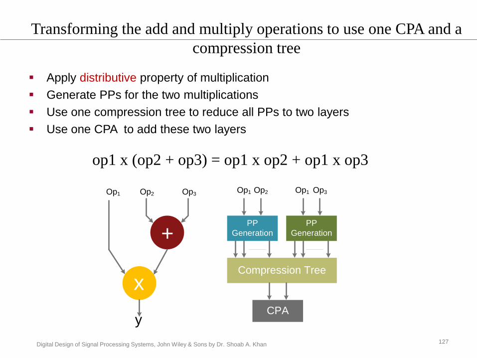
Apply distributive property of multiplication
Generate PPs for the two multiplications
Use one compression tree to reduce all PPs to two layers
Use one CPA to add these two layers
Transforming the add and multiply operations to use one CPA and a
compression tree
+
x
Op2 Op3
y
Compression Tree
CPA
Op1 Op2 Op1Op1
PP
Generation
PP
Generation
Op3
op1 x (op2 + op3) = op1 x op2 + op1 x op3
127

Digital Design of Signal Processing Systems, John Wiley & Sons by Dr. Shoab A. Khan
Transformation to use compression trees and single CPA to
implement a cascade of multiplication operations
128
CT
PPG
Op1 Op2
Prod
PP Generation (PPG)
Op3
PPG
Op3
CT
PPG PPG
Op4 Op4
S1
S2
C1
C2
CT
S3 C3
CPA
x
x
Op1 Op2
x
Op4
Op3x
x
x
Digital Design of Signal Processing Systems, John Wiley & Sons by Dr. Shoab A. Khan
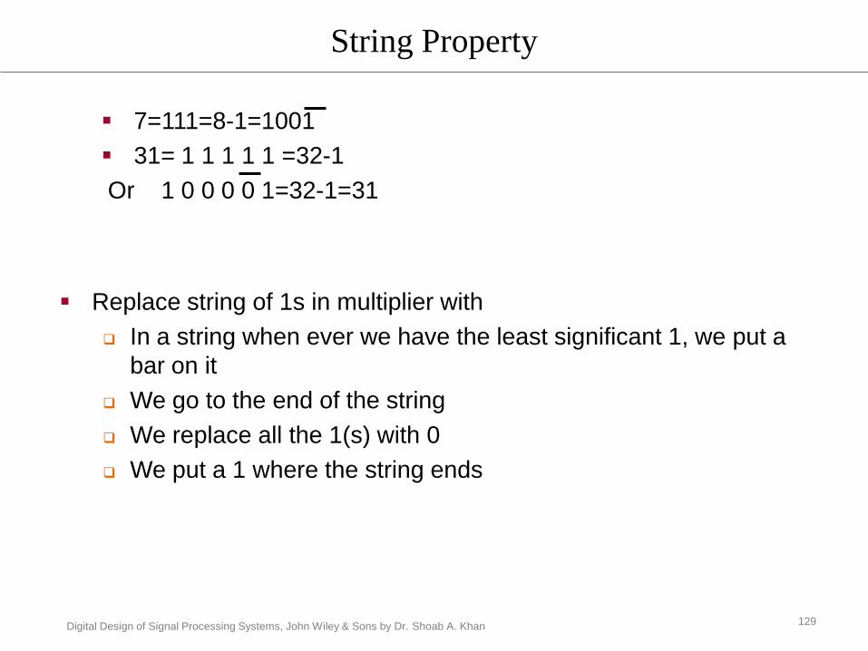
String Property
129
7=111=8-1=1001
31= 1 1 1 1 1 =32-1
Or 1 0 0 0 0 1=32-1=31
Replace string of 1s in multiplier with
In a string when ever we have the least significant 1, we put a
bar on it
We go to the end of the string
We replace all the 1(s) with 0
We put a 1 where the string ends

Digital Design of Signal Processing Systems, John Wiley & Sons by Dr. Shoab A. Khan 130
Instead of multiplying with a single bit
We multiply with two bits hence making the partial
products half in No.

Digital Design of Signal Processing Systems, John Wiley & Sons by Dr. Shoab A. Khan
Booth Recoding Basic Idea
131
A = 1 0 1 0 1 1 0 1
B = 1 0 1 0 1 1 0 1
For these two bits Booth’s algorithm restricts the value to be (-2, -1, 0,
+1,+2)
+2 means Shift left A by one
+1 means Copy A in the answer
0 means copy all 0’s
-1 means 2’s complement and then copy
-2 means 2’s complement and then shift left

Digital Design of Signal Processing Systems, John Wiley & Sons by Dr. Shoab A. Khan
Booth’s Algorithm
132
Form pairs using string property
1 0 1 0 1 1 0 1
Use the MSB of the previous group to check for the string property on
the pair, use 0 for the first pair
0

Digital Design of Signal Processing Systems, John Wiley & Sons by Dr. Shoab A. Khan 133
21=2 20=1
0 0 0 0
0 0 1 1
0 1 0 1
0 1 1 2
1 0 0 -2
1 0 1 -1
1 1 0 -1
1 1 1 0
As the string property is applied on three bits, there are
following eight possibilities: