Transparent Oxides for Electronics: problem of electrical...
14
1 Ekaterine Chikoidze GEMaC, CNRS,Versailles University, France Transparent Oxides for Electronics: problem of electrical transport
-
Upload
dangnguyet -
Category
Documents
-
view
218 -
download
2
Transcript of Transparent Oxides for Electronics: problem of electrical...

1
Ekaterine Chikoidze
GEMaC, CNRS,Versailles University, France
Transparent Oxides for Electronics:
problem of electrical transport

2
OXIDES: Transparent & Conducting
Heat reflecting windows, electrochromic windows, LCD panel, OLED, solar cells,
touch panels ,….
Advantege of oxides:
Higher voltage tolerances;
More stability at high temperatures;
Oxygen tolerance, opening up gas and air monitoring applications;
The ability to make transparent electronics
Magnetic sensors
Goodbye silicon, hello oxides!!!
Expect market value for TCOs in coming years will be more then 200 billions $

3
Figure of Merit for TCO
/ = -Rsln(T+R)-1
R.Gordon MRS Bull.2000
Electrical Conductivity
Optical absorption
The first TCO by J.M.MOCHEL, U.S. PATENT NO.2,564, (1947) 706

4
n type TCO
The cost of the raw materials
Cd < Zn <Ti < Sn <Ag <In
Toxicity of the elements
Zn< Sn < In< Ag < Cd R.Gordon,MRS Bull.2000
ZnO
F
Cl
I
Br
B
Al
Ga
In
Zr
Ti
P
As
VII group
Important criteria for TCO:
1018
1019
1020
0
5
10
15
20
25
30
35 sapphire
fused silica
µ (
V-1s
-1c
m2)
Carrier concentration (cm-3)
ZnO:Cl
Phys. stat. sol. (a) 203,2007
0 50 100 150 200 250
1018
1019
1020
on sapphire
on fused silica
Ca
rrie
r co
nce
ntr
atio
n (
cm
-3)
n-BuCl pressure, (Pa)
By MOCVD
1% Cl
5
n type TCO
AZO by PLD
Thin Solid Films 516 (2008) 8141–8145
Transmittance
T(VIS)=78-82%
T(NIR)≈ 86%
ZnO:Cl
ρ=1.3x10⁻³Ohm cm
n=6.1x1020cm-3
µ=7 cm2/Vs
1 2 3 4 5 610
15
20
25
Ele
ctr
on m
obili
ties, cm
2/V
s
x1021
Carrier Concentration (cm-3)
AZO
2%Al ρ=1.2x10⁻⁴Ohm cm
n=1.2x1021cm-3
µ=18 cm2/VS
T(VIS)=85%

6
p type TCO
WBG metal-oxydes
Most are Insulators ;Few are naturally n-type; rarely naturally p-type
The monopolarity in existing TCOs results from strong localization of positive holes
at oxygen 2p levels or an upper edge of the valence band due to the strong
electronegative nature of oxygen.
Conductivity type inversion in n-type TCO by cation doping SnO2, CdO, ZnO,In2O3….
Difficulty (solubility limit, killer defects, deep levels)
Delocalize holes by reduction of Columb interaction
delafossites : CuAlO2, (Kawazoe et al, 1997)
CuGaO2;CuInO2;CuCrO2;CuBO2; Problem: very high deposition T, indirect band gap
« Chemical modulation of VB »
Transparent p-n junction: oxide with direct band gap, low deposition T,
high quality epi-layers
7
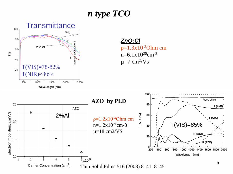
Cu based p type TCO
Cu2O (archetype of Cu based TCO)
V.B.Hybrydised Cu 3d & O2p
localized holes
Polaronic-hopping conduction (R.S.Toth, Phys.Rev. 122,482, 1961;
L.C.Bourne,PRB 40,10973,1989)
D.O.Scanlon, PRL, 103,096405, 2009
K.G.Godhino, J.Matt.Chem.20,1086,2010
SrCu2O2
300 600 900 1200 1500 1800 2100 2400 2700 3000
0
20
40
60
80
100
T [%
]
[nm]
3% Ba doped SCO, Tdep
=450oC, p
O2= 10
-5 mbar
6% Ba doped SCO, Tdep
=350oC, p
O2= 10
-5 mbar
T(VIS)=75-80%
Coll: Tyndall National Institute University College Cork, Ireland;
Thales TRT, France
Delocalization of holes
VCu 3d10Cu(I) 3d9Cu(II)

8
Introducing holes in SrCu2O2 by Ba doping
Hybrid DFT
New localized state in band
gap 1.1 eV above VB
Structure Eg / HSE06
SrCu2O2 3.20 eV
Ba-SrCu2O2 3.24 eV
Ba changes band gap but not the polaronic nature of the material
O
Sr
Cu
SrCu2O2
Holes Predominantly localised on Oxygen atoms
near vacancy site – Polaron
Ba:SrCu2O2
M.Nolan
Tyndall National Institute ,University College Cork, Ireland
9
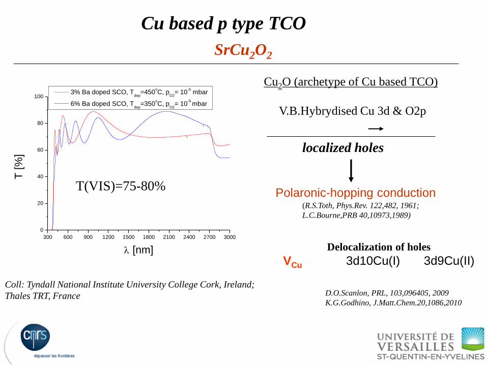
Conduction Mechanism of Ba:SCO
2 4 6 8 10 12 14
-14
-12
-10
-8
-6
-4
-2
0
ln[
(Oh
m.c
m) -1
]
1000/T(K-1)
Ba:SrCu2O
2
3%Ba
Ea=0.12eV = 1+2
NNH
1= 0 exp(-WH/kBT)
Constant Activation energy
Ea=[Ea(p(T));Ea(µ(T)]
Ea=Ea(µ(T)]=WH polaron hopping energy WH=120 meV
polaron binding energy Ep=240eV
0.15 0.20 0.25 0.30 0.35
-14
-12
-10
-8
-6
-4
-2
0
2
ln[
(Oh
m.c
m)-1
]
1/T1/4
(K)-1/4
VRH
2= 0 exp(T0/T)-1/4
Activation energy
T0 ~β/kNEf r p
T0=9x10⁴K
Mobility is thermally activated
1
2
Polaron conductivity
@300K ρ=79 Ω.cm
σ=1.2x10⁻²Scm-1
p= ~1017cm-3
µ<1 V-1s-1cm2

10
Influence of Ba doping on Conductivity of SCO
%Ba
0 (Scm-1)
1x10⁻³
µH(cm2/VS) Ep eV
Polaron
binding energy
3 3x10⁻² <1 240
6 1.2x10⁻² <1 180
Ba:SCO keeps good transparancy in VIS (with small open of Gap)
Ba doping induces less localised holes
Problem remains: low mobility of carriers
Delocalization of carriers by doping another dopant?
11
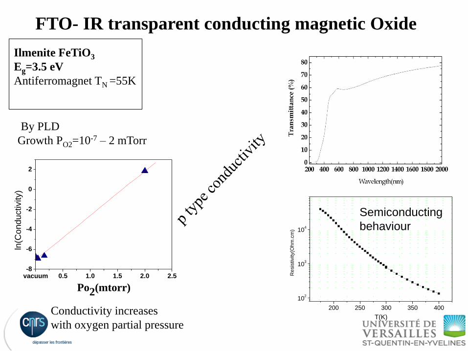
Ilmenite FeTiO3
Eg=3.5 eV
Antiferromagnet TN =55K
By PLD
Growth PO2=10-7 – 2 mTorr
vacuum 0.5 1.0 1.5 2.0 2.5-8
-6
-4
-2
0
2
ln(C
onductivity)
Po2(mtorr)
Conductivity increases
with oxygen partial pressure
200 250 300 350 400
102
103
104
Re
sis
tivity(O
hm
.cm
)
T(K)
Semiconducting
behaviour
FTO- IR transparent conducting magnetic Oxide

12
Thermodynamical analyses
-20 -18 -16 -14 -12 -10 -8 -6 -4 -2 0 2
10
11
12
13
14
15
16
17
18
Ppa
B2
[VFe
']= p[VFe
']= [VO2
.][V
O2
.],=n
[VFe
']
[VO2
.], n
p
log
co
ncen
trati
on
(c
m-3
)
log PO2
(atm)
p
n
[VFe']
[VO2.][V
Fe'], [V
O2
.]
[VFe
'], p
[VO2
.]
n
Pna
B2
n type p type insulator
T=4400C Experiment:
Treatment in oxygen atmosphere
PO2=5.6x10⁻⁴atm
p
PO2=2x10-13atm
n
Coll: T.Tchelidze, TSU, Georgia
Conductivity type inversion
Conductivity type inversion in FTO
Hole conductivity PO2>6x10⁻⁵atm
Electron conductivity PO2<3x10-13atm

13
Conclusion:
Present challenge is to get low temperature deposition of
high quality p type type TCO…..
Future belongs to
‘‘Invisible Electronics’’
14
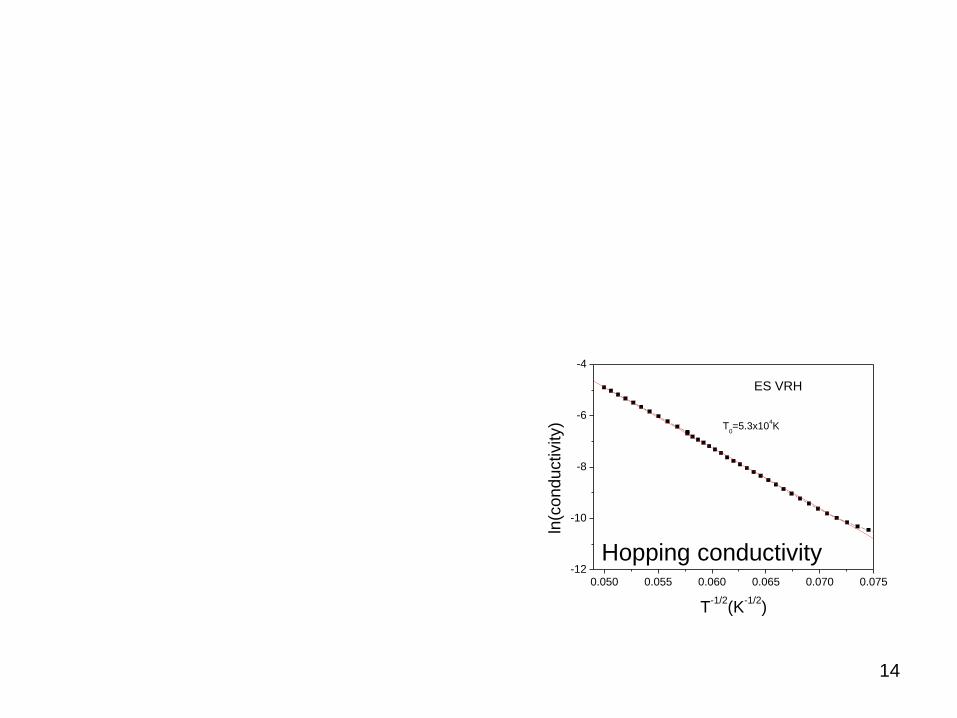
0.050 0.055 0.060 0.065 0.070 0.075-12
-10
-8
-6
-4
ln(c
ond
uctivity)
T-1/2
(K-1/2
)
T0=5.3x10
4K
ES VRH
Hopping conductivity