Transient Simulation of GaN HEMTspublications.lib.chalmers.se/records/fulltext/179391/179391.pdf ·...
49
Transient Simulation of GaN HEMTs Thesis for Erasmus Mundus Master’s degree in Nanoscience and Nanotechnology SHREETU SHRESTHA Microwave Electronics Laboratory Department of Microtechnology and Nanoscience CHALMERS UNIVERSITY OF TECHNOLOGY Gothenburg, Sweden, 2013
Transcript of Transient Simulation of GaN HEMTspublications.lib.chalmers.se/records/fulltext/179391/179391.pdf ·...

Transient Simulation of GaN
HEMTs Thesis for Erasmus Mundus Master’s degree in Nanoscience and Nanotechnology
SHREETU SHRESTHA
Microwave Electronics Laboratory
Department of Microtechnology and Nanoscience
CHALMERS UNIVERSITY OF TECHNOLOGY
Gothenburg, Sweden, 2013


Thesis for Erasmus Mundus Master’s degree in Nanoscience andNanotechnology
Transient Simulation of GaN HEMTs
SHREETU SHRESTHA
Microwave Electronics Laboratory
Department of Microtechnology and Nanoscience - MC2
CHALMERS UNIVERSITY OF TECHNOLOGY
Goteborg, Sweden 2013
Transient Simulation of GaN HEMTsShreetu Shrestha
© Shreetu Shrestha, 2013
Microwave Electronics LaboratoryDepartment of Microtechnology and Nanoscience - MC2Chalmers Univeristy of TechnologySE-412 96 GoteborgSwedenTelephone + 46 (0)31-772 1000
This report is written in LATEX
Chalmers ReproserviceGoteborg, Sweden 2013

Abstract
Subthreshold drain leakage can be suppressed in GaN HEMTs by intentionallydoping the GaN buffer with deep acceptor dopants such as C and Fe or by usinga double heterostructure. In this thesis, both concepts, doping and using doubleheterostructure were investigated using numerical device simulation. The mainfocus was on the study of transient electrical behaviour and the understandingof trapping behaviour of deep acceptor dopants which causes current collapse.It was found that current collapse is dependent on dopant concentration and isworse with Fe doping than with C doping. These results were explained by con-sidering the potential barrier formed in the GaN buffer due to electron trapping.Transistors with an undoped GaN channel layer on top of a doped GaN bufferlayer had a small current collapse but much a higher drain current.
Keywords: GaN/AlGaN, HEMT, current collapse
i

ii

Contents
Abstract i
1 Introduction 1
2 Theory 32.1 Polarisation . . . . . . . . . . . . . . . . . . . . . . . . . . . . . . 32.2 AlGaN/GaN HEMT . . . . . . . . . . . . . . . . . . . . . . . . . 42.3 Trap Dynamics . . . . . . . . . . . . . . . . . . . . . . . . . . . . 52.4 Current Collapse . . . . . . . . . . . . . . . . . . . . . . . . . . . 6
3 Simulation 93.1 Simulation software . . . . . . . . . . . . . . . . . . . . . . . . . . 93.2 Device Structure and parameters . . . . . . . . . . . . . . . . . . 103.3 Physical models . . . . . . . . . . . . . . . . . . . . . . . . . . . . 113.4 Trap Definition . . . . . . . . . . . . . . . . . . . . . . . . . . . . 13
4 Results 154.1 AlGaN/GaN:[C] HEMTs . . . . . . . . . . . . . . . . . . . . . . . 15
4.1.1 DC characterisation . . . . . . . . . . . . . . . . . . . . . 164.1.2 Transient pulsed simulation . . . . . . . . . . . . . . . . . 17
4.2 AlGaN/GaN:[Fe] HEMTs . . . . . . . . . . . . . . . . . . . . . . 224.2.1 DC characterisation . . . . . . . . . . . . . . . . . . . . . 224.2.2 Transient pulsed simulation . . . . . . . . . . . . . . . . . 244.2.3 Trap energy level and thermal effects . . . . . . . . . . . . 25
4.3 AlGaN/GaN/GaN:[C] HEMTs . . . . . . . . . . . . . . . . . . . 274.3.1 DC characterisation . . . . . . . . . . . . . . . . . . . . . 284.3.2 Transient pulsed simulation . . . . . . . . . . . . . . . . . 28
4.4 AlGaN/GaN/AlGaN DH-HEMTs . . . . . . . . . . . . . . . . . . 304.4.1 DC characterisation . . . . . . . . . . . . . . . . . . . . . 304.4.2 Transient pulsed simulation . . . . . . . . . . . . . . . . . 32
5 Conclusion 35
Acknowledgements 36
References 39
iii

iv

Chapter 1
Introduction
GaN based HEMTs have attracted considerable attention over the last decade.First fabricated in 1993 [1], GaN based HEMTs have been commercially avail-able since 2005 [2]. The major application areas today include RF and mi-crowave electronics [3].
GaN has several advantages over conventional III-V semiconductors. With awide bandgap of 3.4 eV, GaN based HEMTs can be operated at high electricfields and high temperatures. The electron density in the channel is also higherin comparison to other III-V semiconductors like GaAs. Although the low-fieldmobility of electrons in GaN bulk is lower than that of GaAs, GaN has a largersaturation velocity. Due to these qualities, GaN HEMTs are suitable candidatesfor high power and high voltage applications.
One of the concerns with GaN HEMTs is the subthreshold drain leakage athigh drain-source bias. Electrons can punch through the GaN buffer at highelectric fields. This effect can be suppressed by intentionally doping the GaNbuffer with deep acceptor impurities such as C and Fe which trap electronsand reduce current leakage. These traps however, also cause unwanted memoryeffects resulting in current collapse; a phenomenon described as a temporarydecrease in current due to trapping of electrons. It is important to address suchnonlinear behaviour because it severely limits the output power performance [4].As an alternative to doping, a double heterostructure which confines electronsin the channel can also be used to minimize current leakage.
In this thesis, both concepts, doping and using double heterostructure areinvestigated using numerical device simulation. The main focus is on thestudy of transient electrical behaviour and understanding of trapping dynam-ics which causes current collapse. A brief background of GaN HEMTs andtrap dynamic is given in Chapter 2. The simulation setup, models and pa-rameters are covered in Chapter 3. The result section, Chapter 4, is di-vided into four groups; AlGaN/GaN:[C] HEMTs, AlGaN/GaN:[Fe] HEMTs,AlGaN/GaN/GaN:[C] HEMTs and AlGaN/GaN/AlGaN HEMTs. DC andtransient pulsed simulation results are discussed for all the four device struc-tures. Finally, the results are summarized and a conclusion is drawn in Chapter5.
1

2 CHAPTER 1. INTRODUCTION

Chapter 2
Theory
2.1 Polarisation
The unit cell of GaN with hexagonal wurtzite structure is shown in Fig. 2.1.The spacing between two hexagonal lattice planes is defined by c, the distanceof atoms in the hexagonal plane is defined by a and the bond length along thec-axis is defined by u [5]. For an ideal hexagonal wurtzite structure, the latticeconstant ratio c/a is
√8/3, and u is 3/8 [6]. However, due to the internal
Figure 2.1: Hexagonal wurtzite crystal structure of GaN. Picture taken from [7]
asymmetry along the c-axis of GaN crystal the c/a ratio differs from the idealvalue giving rise to spontaneous polarization [8]. This is an intrinsic propertyof the material and exists even in bulk.
Piezoelectric polarization, on the other hand, is induced by mechanical strain.The lattice constant of AlGaN is smaller than that of GaN. Due to this differ-ence the thin AlGaN layer is strained which gives rise to piezoelectric polariza-tion.
3

4 CHAPTER 2. THEORY
2.2 AlGaN/GaN HEMT
The high polarization in AlGaN/GaN heterostructure results in a high electricfield which produces a high charge density at the interface. Free electrons tendto compensate this polarization induced charge. A two-dimensional electrongas (2DEG) is thus formed at the AlGaN/GaN interface provided that theconduction band offset is reasonably high [9].
Unlike other conventional HEMTs, intentional doping is not required in GaNHEMTs due to high internal polarisation. A sheet carrier concentration of1013 cm−3 can be achieved without any intentional doping. There are differenttheories explaining the origin of the electrons in 2DEG but it is generally agreedthat they come from the donor states on the AlGaN surface [10,11].
Fig. 2.2 shows the device structure of a typical AlGaN/GaN HEMT. The currentflows from the Ohmic drain contact through the 2DEG channel to the Ohmicsource contact. The size of the channel is controlled by the voltage applied atthe Schottky gate contact. The sheet carrier concentration ns varies along thechannel as [12]
ns (x) =σ (x)e−(ε0ε (x)de2
)[eφb (x) + EF (x)−∆Ec (x)] , (2.1)
where σ (x) is the positive piezoelectric sheet charge density, ε is the dielectricconstant of AlGaN, d is the width of the AlGaN barrier, eφb is the Schottkybarrier of the gate contact, EF (x) is the Fermi level with respect to the GaNconduction band and ∆Ec (x) is the conduction band offset at the interface.AlGaN/GaN HEMTs are normally on device. Therefore, a negative gate voltagelarger than the threshold voltage has to be applied to pinch off the channel asshown in Fig. 2.3.
Figure 2.2: AlGaN/GaN HEMTs device structure with energy of conduction band(blue) and electron density (red). Picture taken from [13].
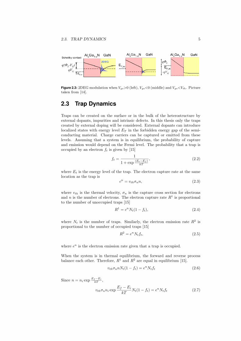
2.3. TRAP DYNAMICS 5
Figure 2.3: 2DEG modulation when Vgs>0 (left), Vgs<0 (middle) and Vgs<Vth. Picturetaken from [14].
2.3 Trap Dynamics
Traps can be created on the surface or in the bulk of the heterostructure byexternal dopants, impurities and intrinsic defects. In this thesis only the trapscreated by external doping will be considered. External dopants can introducelocalized states with energy level ET in the forbidden energy gap of the semi-conducting material. Charge carriers can be captured or emitted from theselevels. Assuming that a system is in equilibrium, the probability of captureand emission would depend on the Fermi level. The probability that a trap isoccupied by an electron ft is given by [15]
ft =1
1 + exp (Et−Ef )kT
, (2.2)
where Et is the energy level of the trap. The electron capture rate at the samelocation as the trap is
cn = vthσnn, (2.3)
where vth is the thermal velocity, σn is the capture cross section for electronsand n is the number of electrons. The electron capture rate R1 is proportionalto the number of unoccupied traps [15]
R1 = cnNt(1− ft), (2.4)
where Nt is the number of traps. Similarly, the electron emission rate R2 isproportional to the number of occupied traps [15]
R2 = enNtft, (2.5)
where en is the electron emission rate given that a trap is occupied.
When the system is in thermal equilibrium, the forward and reverse processbalance each other. Therefore, R1 and R2 are equal in equilibrium [15].
vthσnnNt(1− ft) = enNtft (2.6)
Since n = ni exp Ef−EikT ,
vthσnni expEf − EikT
Nt(1− ft) = enNtft (2.7)

6 CHAPTER 2. THEORY
From Eq. 2.2, 1−ftft
= exp Et−EfkT , so
en = vthσnni expEt − EikT
(2.8)
Since Eq. [2.8] does not depend on the electron occupation probability ft (andthe Fermi level), it is valid even in nonequilibrium conditions although it wasderived using equilibrium assumptions. This equation shows that there is anexponential relationship between trap energy level and emission rate. Trapswith energy level closer to the conduction band have a higher electron emissionrate.
2.4 Current Collapse
Current collapse refers to the temporary reduction in drain current after theapplication of a high drain-source bias [4]. Fig. 2.4 shows an average of about800 pulsed measurement results of AlGaN/GaN HEMT for drain voltage pulsedfrom 15 V to 30 V. When the drain voltage is pulsed to 30 V for 0 µs, electronsfrom the channel are accelerated and penetrate the GaN buffer where theyget captured by traps. Due to the trapping of electrons, the drain currentdecreases.
Figure 2.4: Average measured transient drain current responce at Vgs = -1.8 V, Vds
pulsed from 15 V to 30 V. Measurements taken by Daniel Niessen.
The electrons remain trapped for a while even after the drain voltage is pulsedback to 15 V. Therefore, the drain current level after the pulse is lower thanthat before the pulse. The trapped electrons can be emitted by stimulus like

2.4. CURRENT COLLAPSE 7
light or heat which assists them to overcome the emission barrier and return tothe channel [4]. Thus, this is a recoverable phenomenon as the drain currenteventually comes back to its equilibrium level.
Current collapse is observed in other semiconductor devices like AlGaAs/GaAsHEMTs as well. However, it is more problematic in GaN based HEMTs dueto the high operating voltage and the relative immaturity of GaN technol-ogy.

8 CHAPTER 2. THEORY

Chapter 3
Simulation
3.1 Simulation software
Synopsys TCAD was used to perform numerical device simulations. Synopsysprovides a number of tools for simulating devices, managing simulation tasksand analysing simulation results [16]. The following tools were used in thisproject:
Sentaurus structure editor (SSE) creates 2D and 3D device structures. Thestructure of a device is approximated by a ”mesh” consisting of a large numberof elements. Continuous physical quantities like electric field and temperatureare converted into discrete elements of a mesh. A higher mesh density givesa more accurate and precise result but at the cost of a higher computationtime. Therefore, denser meshes were used only in the regions where the currentdensity and electric field was expected to be high as shown in Fig.3.1. Meshingstrategies and doping profiles were defined using SSE.
Figure 3.1: HEMT structure with Mesh created in SSE. The mesh density is higher atthe interface.
Sentaurus Device (SD) solves the Poisson’s equation and the carrier continu-ity equations for given boundary conditions and device structure. The softwareuses numerical solvers which iterates repeatedly until a solution with desiredaccuracy is obtained [17]. Models defining mobility, bandgap, recombinationand other physical properties were specified in SD.
9

10 CHAPTER 3. SIMULATION
Visualisation software Inspec was used to plot I-V characteristics. SentaurusVisual (SV) was used to visualise 2D output data from the simulation for currentdensity, trap occupation, band diagram and others.
Sentaurus work bench (SWB) provides a graphical user interface to inte-grate all other Synopsys tools. SWB was used as a framework to create, manage,execute and analyse TCAD simulations [16].
Figure 3.2: Simulation tool workflow with important input and output files
3.2 Device Structure and parameters
The schematic of the simulated AlGaN/GaN HEMT structure is shown in Fig.3.3. 20 nm thick Al0.25Ga0.75N barrier layer on top of 2 µm thick GaN bufferlayer was simulated. Some properties of the materials used are given in Table.3.1.
Table 3.1: Material properties of GaN, Al0.25Ga0.75N and SiC [18–22]
GaN Al0.25Ga0.75N SiC
Relative Permittivity ‖ to c-axis 10.4 10.13 9.8⊥ to c-axis 9.5 9.06 9.8
Bandgap at 300 K (eV) 3.40 4.10 3.19Electron affinity at 300 K (eV) 3.44 3.05 4.10
The polarization effect was modelled with a fixed positive density charge of1.39 × 1013 cm−2 at the AlGaN/GaN interface and a fixed negative chargedensity of 3.20× 1013 cm−2 at the AlGaN/Si3N4 interface [9].
A donor trap sheet density of 1×1014 cm−2 was set at the Si3N4/AlGaN-barrierinterface. The surface barrier (φs), which is the difference between the AlGaN-barrier conduction band and Fermi level at the surface, was modelled as a singledonor energy level equivalent to 1.78 eV below conduction band [23]. Drain

3.3. PHYSICAL MODELS 11
Figure 3.3: Simulated device strucure (not drawn to scale)
and source contacts were modelled as Ohmic metal/semiconductor interface onheavily doped AlGaN region. A doping concentration of 1× 1020 cm−3 was setin the AlGaN regions under the contacts.
The interface between two materials were modelled as heterointerface. Fermi-Dirac distribution statistics and Shockley-Read-Hall recombination were en-abled. The temperature was fixed to 298 K and background doping was notconsidered.
3.3 Physical models
Sentaurus device allows us to choose from a variety of different physical models.Some important models that were used in this thesis are described below
Drift Diffusion model
The drift diffusion (DD) model is based on the method of moments solution ofthe Boltzmann’s transport equation (BTE) [24]. The basic idea of BTE is thatthe time rate of change of probability distribution function, f , is proportionalto the scattering events [24].
df
dt={∂f
∂t
}scattering
(3.1)
By applying relaxation time approximation, BTE can be expressed as [24]
df
dt= ∇rf · vg +∇kf ·
F~
=f − f0τ
(3.2)
where vg is the group velocity of distribution, ∇r and∇k are the gradient in realspace and momentum, F is the applied force and f0 is the distribution function

12 CHAPTER 3. SIMULATION
at thermal equilibrium. Moments of the BTE are obtained by multiplying Eq.3.2by a quantity to be conserved and integrating over all k space [24]. The firstmoment, where the the quantity to be conserved is the particle number, givesthe current continuity equations
∇ · Jn = qR+ q∂n
∂t(3.3)
−∇ · Jp = qR+ q∂p
∂t(3.4)
where Jn is the electron current density, Jp is the hole current density and Ris the net recombination rate. The DD equation takes into account the firsttwo moments of BTE. The current density is expressed as a sum of drift anddiffusion term as [25]
Jn = nqµn∇E + qDn∇n (3.5)
Jp = pqµp∇E− qDp∇p (3.6)
where µn and µp are the electron and hole mobility, and Dn and Dp are thecorresponding diffusion coefficients. µn and Dn are related by the Einsteinrelation [25]
Dn = µnkT
q(3.7)
From 3.7, 3.5 and 3.6, the current density can be finally expressed in terms ofquasi-Fermi potentials as [25]
Jn = −nqµn∇φn (3.8)
Jp = −pqµp∇φp (3.9)
SD also offers other transport models. The Hydrodynamic model (HD), forexample, considers the first 4 moments of BTE and is thus physically moreaccurate. However, to reduce the complexity and save computation time, onlythe basic drift-diffusion model was used in this project.
Mobility model
Fig. 3.4 shows the velocity of various semiconductors as a function of electricfield. The electron velocity in Si and SiC increases with an increase in electricfield and then saturates at high fields. The electron velocity in AlGaN/GaNinterface however, does not saturate but continues to increase at slower rateand then decreases.
Therefore, a mobility model with two linear regions described in [27] was usedfor AlGaN/GaN. This model takes into account the electric field and also thelattice temperature. The mobility is given by
µ(T,E) =µLF
β
√1 +
(µLFE
v0+µHFE
)β (3.10)

3.4. TRAP DEFINITION 13
Figure 3.4: Electron velocity as a function of electric field for various semiconductors(Nd = 1017 cm−3). Picture taken from [26]
=µLF0
(TT0
)−µLFexpβ0( T
T0 )−βexp
√√√√√1 +
(µLF0
(TT0
)−µLFexpE
v00(TT0
)−v0exp+µHF0
(TT0
)−µHFexpE
)β0
(TT0
)−βexp (3.11)
where E is the electric field parallel to the current, µLF is the differential mo-bility at low electric fields, v0 is the intersection of extrapolated high field withthe y-axis, and β governs the smoothness of the transition between the low-fieldand high-field regions. The temperature dependence is modelled by the expo-nents µLFexp, µHFexp, v0exp and βexp. β0, µLF0, µHF0 and v00 are values atT0 [27].
3.4 Trap Definition
Acceptor type traps were simulated in the GaN buffer layer. These traps areneutral when unoccupied and carry the charge of one electron when occupied.The traps were uniformly distributed in the GaN buffer. The energy of thetraps was set to a single specified level. In literature, different values of thetrap energy level for C [28] and Fe [29] doping can be found. While the exactvalue of the trap energy level is in debate, there is a general agreement thatC traps form acceptor levels in the lower half of the energy gap and Fe trapsform acceptor levels in the upper half of the energy gap. In this thesis, C andFe trap energy levels were set to 0.9 eV [30] and 2.9 eV [31] above the valance

14 CHAPTER 3. SIMULATION
band respectively. The capture cross section was set to 1× 10⁻¹⁵ cm2 for bothC and Fe traps [32].
The electron capture rate from the conduction band cnC at a location same asthe trap is simulated as [33]
cnC = σnvthn, (3.12)
where σn is the electron capture cross section, vth is the thermal velocity and nis the electron density. Similarly, the electron emission rate to the conductionband is simulated as [33]
enC = σnvthNC exp[(Etrap − EC)
kT], (3.13)
where NC is the electron density of state, Etrap is the trap energy level andEC is the conduction band energy.

Chapter 4
Results
Four different transistor were investigated; AlGaN/GaN:[C] HEMTs,AlGaN/GaN:[Fe] HEMTs, AlGaN/GaN/GaN:[C] HEMTs andAlGaN/GaN/AlGaN. DC and transient pulsed simulation results for allfour transistors will be discussed in this section.
4.1 AlGaN/GaN:[C] HEMTs
The simulated I-V curves for AlGaN/GaN HEMTs with 20 nm thickAl0.25Ga0.75N barrier layer and 2 µm thick GaN buffer layer are shown in Fig.4.1.
(a) (b)
Figure 4.1: Simulated I-V curves for AlGaN/GaN HEMTs (a) IDS-VDS (b)IDS-VGS
Subthreshold drain leakage current can be observed for Vds = 10 V in Fig. 4.1bdue to the punch-through effect. Even when the channel is pinched off, electrons
15

16 CHAPTER 4. RESULTS
can flow through the GaN buffer under the depleted channel at high Vds. Thisleakage current can be suppressed by doping the GaN buffer with deep acceptorimpurities which trap electrons. Two commonly used dopants in GaN HEMTsare C and Fe. In this section, the DC and transient characteristics with C dopedGaN buffer will be discussed.
4.1.1 DC characterisation
Fig. 4.2 shows the I-V curves for AlGaN/GaN HEMTs with 1 × 1016 cm−3 Cdopants in the GaN buffer. It can be seen that drain current is lower with Cdoping than without any doping. The drain leakage current at Vds = 10 V issuppressed and the output resistance is higher.
(a) (b)
Figure 4.2: I-V curves for AlGaN/GaN HEMTs with 1× 10¹⁶ C doped GaN buffer (a)Ids-Vds (b)Ids-Vgs
Similar plots were simulated for AlGaN/GaN HEMTs with 1 × 1017 cm−3 Cdoped GaN buffer. The I-V curves for the three different cases are compared inFig.4.3. It can be seen that the drain current further decreases with 1 × 10¹⁷
cm−3 C doping. The Vth increases from −4.1 V for 1× 10¹⁶ C doping to −3.4V for 1× 10¹⁷ doping.
These results can be explained by considering the trapping behaviour of C im-purities. The traps created by C dopants in the GaN buffer capture electronsfrom the 2DEG channel. Therefore, the electron density is lower which resultsin a lower drain current. With more dopants, more electrons from the chan-nel are trapped in the buffer. Therefore, the drain current decreases as the Cconcentration increases.
The increase in Vth and output resistance with higher doping is due to the in-crease in buffer potential as shown in Fig. 4.4a. As mentioned earlier, occupiedtraps carry a charge of one electron. This negative charge in the buffer increasesthe potential barrier. As a result, the subthreshold drain leakage through the

4.1. ALGAN/GAN:[C] HEMTS 17
(a) (b)
Figure 4.3: I-V curves for AlGaN/GaN HEMTs with no doping, 1 × 1016 cm−3 and1×1017 cm−3 C doped GaN buffer (a) Ids-Vds at Vgs =-3 V (b) Ids-Vgs at Vds = 10V
(a) (b)
Figure 4.4: (a)Energy diagram of conduction band at steady state for AlGaN/GaNHEMTs with no doping, 1× 1016 cm−3 and 1× 1017 cm−3 C doped GaN buffer as afunction of distance from the AlGaN/GaN interface (b) 2DEG
buffer is suppressed and Vth is increased. Although a higher dopant concen-tration is desirable to achieve a higher Vth, it also results in a lower draincurrent. Therefore, there is a trade off between higher Vth and higher draincurrent.
4.1.2 Transient pulsed simulation
For transient simulations, the drain voltage was pulsed from 15 V to 30 V for aperiod of 10 µs as shown in Fig.4.5a. The ramping time was set to 10 ns. The

18 CHAPTER 4. RESULTS
gate voltage was kept constant at -4 V.
Fig.4.5b shows the transient simulation results for AlGaN/GaN HEMTs with1× 1016 C doping and no doping. It can be seen that without any doping, thedrain current follows the drain voltage linearly. The current after the pulse isexactly equal to the current before the pulse. This however, is not the casewith 1× 10¹⁶ C traps. When the drain voltage is ramped to 30 V, the currentreaches a maximum value and then decreases. A small peak can be observed asthe current decreases rapidly during the first 2 µs. The drain current after thepulse also goes down by 12.1%.
(a) (b)
Figure 4.5: (a) Drain voltage pulsed from Vdsq= 15 V to Vdsp= 30 V (b) Ids(t) forAlGaN/GaN HEMTs with 116 C doping and no doping at Vgs= -4 V
This can be explained by considering trap dynamics. Before the pulse, thereis an equilibrium between the process of electron capture and emission. Whenthe drain voltage is ramped to 30 V, electrons gain more energy and spill overin the buffer as shown in Fig. 4.6(b). It takes some time for the electrons toget trapped. In the beginning, traps closer to the interface are filled quicklyresulting in a rapid decrease in current. Gradually over time, traps locateddeeper in the bulk are filled.
Figure 4.6: Electron density (a) before, (b) during and (c) after the drain voltage pulseat Vgs=-4 V.

4.1. ALGAN/GAN:[C] HEMTS 19
Once captured, the electrons remain in the traps unless they gain enough energyto go back. When the drain voltage is ramped down to 15 V, a lot of electronswhich were trapped during the pulse still remain trapped in the buffer. Fig.4.7 shows the difference in the density of trapped electrons before and after thepulse. The blue region represents the area where traps that were unoccupiedbefore the pulse were occupied after the pulse. It can be seen that more electronsget trapped below the gate region after the pulse.
Figure 4.7: The difference in occupied trap density before and after the pulse
Therefore the electron density in the channel after the pulse is lower than be-fore as shown in Fig. 4.6. This phenomenon is known as current collapse. Ifthe simulations are run for a longer time it can be observed that the currentgradually increases back to the equilibrium position as the captured electronsare emitted from the traps.
Duration of pulse
(a) (b)
Figure 4.8: (a) Ids(t) when Vgs was pulsed from 15 V to 30 V for 1 µs, 5 µs and 20 µsat a constant Vgs = -4 V (b) zoom in of (a) showing current collapse
Fig. 4.8 shows the transient drain current response when the drain voltage

20 CHAPTER 4. RESULTS
was pulsed from 15 V to 30 V for 1 µs, 5 µs and 20 µs. The Vgs was keptconstant at -4 V. For drain voltage pulse duration of 1 µs, 5 µs and 20 µs, thecurrent collapse was 11.3%, 12.0% and 12.3% respectively. The current collapseincreases with pulse duration because more electrons are trapped over a longerperiod of time. However, the rate of electrons being trapped decreases graduallyas more and more traps are filled. Therefore the difference in current collapsebetween 1 µs and 5 µs is 0.7% while the difference is only 0.3% between 5 µsand 20 µs although the time duration difference is longer.
VDS Dependence
Fig. 4.9a shows the drain current when Vds was pulsed from 5 V to 15 V, 30 Vand 60 V. The Vgs was kept constant at -4 V. It can be seen that for a higherpulse drain voltage, the peak in the drain current is sharper. The reason for thisis that at higher drain voltage electrons have more energy and can penetratedeeper in the buffer in a shorter duration of time. As a result, more electronsget trapped in the buffer. Therefore, the current collapse is higher for a higherVdsp as shown in Fig. 4.9b. For Vdsp 15 V, 30 V and 60 V, the current collapseis 6.9%, 63.8% and 90.2% respectively.
(a) (b)
Figure 4.9: (a) Ids(t) for Vdsp = 15 V, 30 V and 60 V at Vgs = -4 V (b) Current collapse
VGS Dependence
Fig. 4.10a shows the drain current when the drain voltage was pulsed from 15V to 30 V for Vgs = -2 V, -3 V and -4 V. The percentage current collapse fordifferent Vgs is shown in Fig. 4.10b. It can be observed that as the gate voltagedecreased, the current collapse increases. This is because, with a more negativegate voltage the channel is closer to pinch off and there are fewer electrons in thechannel. The electron density for different Vgs can be seen in Fig. 4.11. For a

4.1. ALGAN/GAN:[C] HEMTS 21
(a) (b)
Figure 4.10: (a) Ids(t) for Vgs = -2 V, -3 V and -4 V (b) Percentage current collapsefor different Vgs. Vds pulsed from 15 V to 30 V.
Figure 4.11: Electron desnsity near the AlGaN/GaN interface for differnt Vgs
lower gate voltage there are fewer electrons in the channel and they are sparselydistributed. Therefore, a higher fraction of electrons get trapped.
Doping concentration
Fig. 4.12a shows the drain current for AlGaN/GaN HEMTs with 1×1016 cm−3
and 1×1017 cm−3 C doping concentration in the GaN buffer. Again the Vds waspulsed from 15 V to 30 V and current collapse for different Vgs was calculated.The percentage current collapse for different C doping concentration can beseen in Fig. 4.12b. It can be seen that the current collapse increases whenthe doping concentration is increased from 0.8 × 1016 cm−3 to 1 × 1016 cm−3.

22 CHAPTER 4. RESULTS
(a) (b)
Figure 4.12: (a) Ids(t) with 1× 1016 cm−3 and 1× 1017 cm−3 C doping concentrationVgs= -3 V (b) Percentage current collapse for different Vgs. Vds pulsed from 15 V to30 V.
However, when the dopant concentration was increased further to 1.5 × 10¹⁶
cm−3 and 1× 1017 cm−3the current collapse decreases. This results was ratherunexpected since it was presumed that the current collapse would be worse withmore traps.
These results can be explained by considering the screening effect of occupiedtraps. Traps filled with electrons are negatively charged. As more and moretraps become occupied it gets increasingly difficult for electrons from the channelto penetrate the GaN buffer. The negative charge of the occupied traps confineelectrons in the channel resulting in fewer electrons being trapped.
Fig. 4.13a shows the density of occupied traps after the pulse for 1× 1016 cm−3
and 1× 1017 cm−3 C doping. It can be seen than for 1× 1016 cm−3 C doping,traps located deep in the bulk are fully occupied. For 1× 1017 cm−3 C dopinghowever, fewer traps deep in the buffer are occupied. This can be explained bythe conduction band energy diagram shown in Fig. 4.13b. For 1 × 1016 cm−3
C traps, the conduction band energy near the interface is lower. For 1 × 10¹⁷
cm−3 C traps, the higher density of occupied traps near the channel increasesthe conduction band energy and confines electrons more effectively. Thus itcan be said that after a certain number of traps are occupied, the screeningeffect of occupied traps dominates and limits the electron spillover into theGaN buffer.
4.2 AlGaN/GaN:[Fe] HEMTs
4.2.1 DC characterisation
Fig. 4.14 shows the I-V curves for AlGaN/GaN HEMTs with different con-centrations of C and Fe doping in the GaN buffer. Similar to the case with C

4.2. ALGAN/GAN:[FE] HEMTS 23
(a) (b)
Figure 4.13: (a) Density of trapped electrons after pulse for 1016 cm−3 C doping (top)and 1017 cm−3 C doping (bottom) (b) Energy of conduction band at Vgs= -3 V nearthe drain edge of gate before pulse
doping, the drain current is lower with a higher Fe doping concentration. TheVth also increases from -4.3 V for 1×1016 cm−3 Fe doping to -3.8 V for 1×10¹⁷
cm−3 Fe doping.
In comparison to C doping, the drain current is slightly higher and the Vth islower with Fe doping. This is because the Fe trap energy level (2.9 eV from thevalance band) is higher than C trap energy level (0.9 eV from the valence band).Since Fe trap energy level is closer to the conduction band the probability thata Fe trap is occupied is lower than that for C trap. As a result, with Fe dopingfewer electrons are trapped and the electron density in the channel is higherwhich results in a higher drain current. also increases from -4.3 V for 1× 10¹⁶
(a) (b)
Figure 4.14: I-V curves for AlGaN/GaN HEMTs without doping, 1 × 1016 cm−3 and1× 1017 cm−3 doping concentration of C and Fe (a) Ids-Vds at Vgs =-3 V (b) Ids-Vgs
at Vds = 10V

24 CHAPTER 4. RESULTS
cm−3 Fe doping to -3.8 V for 1× 1017 cm−3 Fe doping.
The conduction band energy diagram for C and Fe doping is shown in Fig.4.15a. Due to the shallower energy level of Fe traps, the increase in conductionband energy is lower with Fe doping. The lower bulk potential along with higherelectron density gives a lower Vth for devices with Fe doping.
(a) (b)
Figure 4.15: (a) Energy diagram of conduction band at steady state for AlGaN/GaNHEMTs with no doping, 1×1016 cm−3 and 1×1017 cm−3 C and Fe doped GaN bufferas a function of distance from the AlGaN/GaN interface (b) zoom in of potential well
4.2.2 Transient pulsed simulation
(a) (b)
Figure 4.16: (a) Ids(t) for C and Fe doping at Vgs= -3 V.(b) Percentage current collapsefor different Vgs. Vds pulsed from 15 V to 30 V.
Fe traps have energy level closer to the conduction band than C traps. Therefore,
4.2. ALGAN/GAN:[FE] HEMTS 25
Fe traps emit electrons faster and the probability that Fe traps are unoccupied ishigher. Since fewer Fe traps are occupied at any given time, the drain current ishigher with Fe doping in comparison to C doping as shown in Fig. 4.16a.
The percentage current collapse with 1×1016 cm−3 Fe and C doping for differentVgs is shown in Fig.4.16b. Since the potential barrier in the bulk with Fe trapsis lower, more electrons can spill over in the buffer during the pulse and gettrapped. As a result, the peak rise in current is bigger and the current collapseis higher with Fe doping.
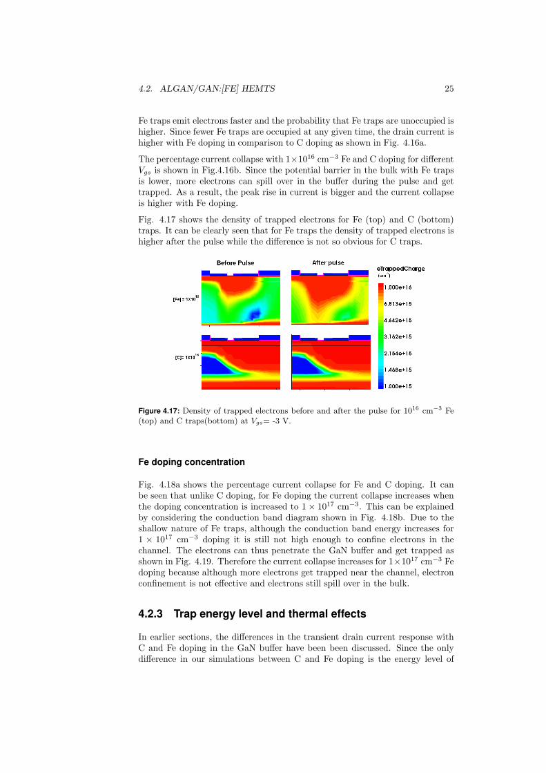
Fig. 4.17 shows the density of trapped electrons for Fe (top) and C (bottom)traps. It can be clearly seen that for Fe traps the density of trapped electrons ishigher after the pulse while the difference is not so obvious for C traps.
Figure 4.17: Density of trapped electrons before and after the pulse for 1016 cm−3 Fe(top) and C traps(bottom) at Vgs= -3 V.
Fe doping concentration
Fig. 4.18a shows the percentage current collapse for Fe and C doping. It canbe seen that unlike C doping, for Fe doping the current collapse increases whenthe doping concentration is increased to 1× 1017 cm−3. This can be explainedby considering the conduction band diagram shown in Fig. 4.18b. Due to theshallow nature of Fe traps, although the conduction band energy increases for1 × 1017 cm−3 doping it is still not high enough to confine electrons in thechannel. The electrons can thus penetrate the GaN buffer and get trapped asshown in Fig. 4.19. Therefore the current collapse increases for 1×1017 cm−3 Fedoping because although more electrons get trapped near the channel, electronconfinement is not effective and electrons still spill over in the bulk.
4.2.3 Trap energy level and thermal effects
In earlier sections, the differences in the transient drain current response withC and Fe doping in the GaN buffer have been been discussed. Since the onlydifference in our simulations between C and Fe doping is the energy level of

26 CHAPTER 4. RESULTS
(a) (b)
Figure 4.18: (a) Percentage current collapse for 1016 cm−3 and 1017 cm−3 C and Fedoping (b) Energy of conduction band at Vgs= -3 V near the drain edge of gate beforepulse
Figure 4.19: Density of trapped electrons before and after the pulse for 1016 cm−3 and1017 cm−3 C and Fe doping at Vgs= -3 V
traps formed, it can be said that the transient response is very sensitive to thetrap energy level. Fig. 4.20 shows the drain current for 1016 cm−3 traps withdifferent energy levels. It can be seen that for traps with energy level closer tothe conduction band, the drain current recovers to the equilibrium level faster.The reason for this is that there is an exponential relationship between emissionof trapped electrons and the difference between the trap and the conductionband energy level (as given in Eq. 3.13). Therefore, electrons are emittedfaster from shallower traps and as a result the drain current goes back to theequilibrium level in a shorter duration of time.
The emission of trapped electrons is also thermally activated (as given in Eq.3.13). Fig. 4.21 shows drain current and average lattice temperature for 1×10¹⁶
cm−3 trap concentration with trap energy level ET = 3 eV. Without thermal

4.3. ALGAN/GAN/GAN:[C] HEMTS 27
Figure 4.20: Ids(t) for 1 × 1016 cm−3 trap concentration with trap energy level, ET =0.9 eV, 2 eV, 2.9 eV, 3 eV, 3.05 eV and 3.1 eV at Vgs= -4 V.
effects the lattice temperature is set to a fixed value of 298 K. It can be seenthat with thermal effects the maximum lattice temperature increases from 340K before the pulse to 430 K during the pulse. Therefore, before the pulsefewer electrons are trapped and the equilibrium current level is higher. Duringthe pulse the drain current decreases faster because of mobility degradation ofelectrons at higher temperature. Similarly after the pulse, the drain current re-covers faster because of the additional thermal energy which assists the emissionof trapped electrons. The electron mobility also increases as the device coolsdown.
Figure 4.21: Ids(t) for 1 × 1016 cm−3 trap concentration with trap energy level, ET =3 eV with and without thermal effects at Vgs= -4 V.
4.3 AlGaN/GaN/GaN:[C] HEMTs
In Section 4.1, it was found that current collapse is negligible with 1×1017 cm−3
C doping in the GaN buffer. However, the drain current with 1 × 1017 cm−3

28 CHAPTER 4. RESULTS
C doping is low. Inorder to minimize current collapse and increase the draincurrent at the same time, a thin undoped GaN channel layer on top of C dopedGaN buffer was used as shown in Fig. 4.22a. Since the doped layer is furtheraway from the channel, fewer electrons are trapped. In this section the DC andtransient pulsed simulation results for AlGaN/GaN/GaN:[C] with thickness ofthe undoped GaN layer d = 50 nm, 200 nm and 500 nm were simulated. Thetotal thickness of the buffer was kept constant. 1 × 1017 cm−3 C doping wasused in the GaN:[C] layer.
4.3.1 DC characterisation
Fig. 4.23 shows the I-V curves for different thickness of undopped GaN layer.It can be seen that as we increase the thickness of the undoped layer, the draincurrent increases. The Vth is -3.4 V, -3.8 V, -3.9 V and -4.2 V for d= 0 nm, 50nm, 200 nm and 500 nm respectively. This is because with a thicker undopedGaN layer, there are fewer traps and they are located further away from thechannel. As a result the electron density in the channel is higher but at thesame time the Vth is lower since the potential barrier underneath the channel islower as shown in Fig. 4.22b.
(a) (b)
Figure 4.22: (a) AlGaN/GaN/GaN:[C] HEMTs device structure (b) Energy diagram ofconduction band for d = 0, 50 nm, 200 nm and 500 nm.
4.3.2 Transient pulsed simulation
Fig. 4.24a shows the drain current for d = 0, 50 nm, 200 nm and 500 nm. Thepercentage current collapse with a higher value of d is higher as shown in Fig.4.24b. This is because with a thicker undoped layer the traps are located furtheraway from the channel and so fewer electrons are trapped before the pulse. As aresult, the buffer potential and the screening effect of trapped electrons is lower.When the pulse is turned on, a larger number of electrons can penetrate thebuffer and get trapped.

4.3. ALGAN/GAN/GAN:[C] HEMTS 29
(a) (b)
Figure 4.23: I-V curves for AlGaN/GaN/GaN:[C] HEMTs with different thickness ofundoped GaN layer d (a) Ids-Vds curves at Vgs =-3 V (b) Ids-Vgs curves at Vds =10 V
(a) (b)
Figure 4.24: (a) Current collapse for different thickness of undoped layer d at Vgs= -3V(b) Percentage current collapse as a function of Vgs
Fig. 4.25a shows that the density of trapped electrons before and after the pulseis the same for d = 0 at Vgs= -3.5 V. But for d= 500 nm the density of trappedelectrons increases after the pulse.
At higher Vgs however the percentage current collapse goes to 0 again. Thisis because since the Vgs is higher, there are more electrons captured before thepulse to provide a better electron confinement. Therefore, fewer electrons aretrapped during the pulse. Fig. 4.25b shows that there is no change in densityof trapped electrons for d = 500 nm at Vgs = -1.5 V.
Although AlGaN/GaN/GaN:[C] HEMTs with thicker undoped GaN layer suffer

30 CHAPTER 4. RESULTS
(a) (b)
Figure 4.25: Density of trapped electrons as a function of distance before the pulse(smooth line) and after the pulse (with x marker) at (a)Vgs= -3.5 V (b) Vgs= -1.5 V
from higher current collapse (at lower Vgs) and have a lower Vth in comparison touniformly doped buffer, they also give a higher conductivity. The drain currentwith d= 500 nm at Vgs= -3 V is about 200% higher than with d= 0. Consideringthis, it might still be worthwhile to use an undoped layer.
Furthermore, the mobility degradation with higher doping has not been consid-ered in the mobility model used in this project. In reality, mobility of electronsin the channel decreases due to scattering caused by collision with dopants. Ifthis is taken into account the current without an undoped GaN layer will beeven lower.
4.4 AlGaN/GaN/AlGaN DH-HEMTs
Another technique to suppress subthreshold drain leakage current is to use awide bandgap material as a backbarrier. A higher buffer potential prevents elec-trons from penetrating into the buffer and hence provides a better confinement.In this section the DC and transient pulsed simulation results of AlGaN/GaNHEMTs with AlGaN backbarrier will be discussed. Different thickness of theGaN channel layer d and Al mole fraction in AlGaN backbarrier will be inves-tigated.
4.4.1 DC characterisation
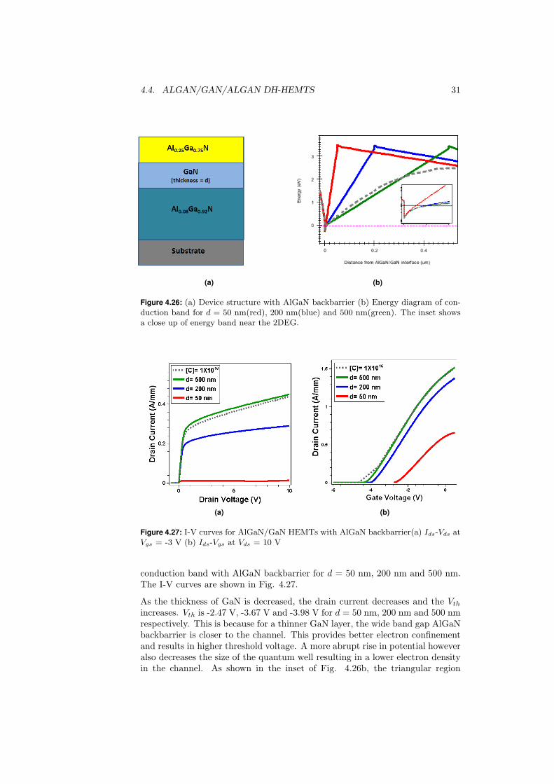
GaN Thickness
The thickness of the undoped GaN layer d was varied while the total thicknessof the buffer was kept constant. Fig. 4.26b shows the energy diagram of
4.4. ALGAN/GAN/ALGAN DH-HEMTS 31
(a) (b)
Figure 4.26: (a) Device structure with AlGaN backbarrier (b) Energy diagram of con-duction band for d = 50 nm(red), 200 nm(blue) and 500 nm(green). The inset showsa close up of energy band near the 2DEG.
(a) (b)
Figure 4.27: I-V curves for AlGaN/GaN HEMTs with AlGaN backbarrier(a) Ids-Vds atVgs = -3 V (b) Ids-Vgs at Vds = 10 V
conduction band with AlGaN backbarrier for d = 50 nm, 200 nm and 500 nm.The I-V curves are shown in Fig. 4.27.
As the thickness of GaN is decreased, the drain current decreases and the Vthincreases. Vth is -2.47 V, -3.67 V and -3.98 V for d = 50 nm, 200 nm and 500 nmrespectively. This is because for a thinner GaN layer, the wide band gap AlGaNbackbarrier is closer to the channel. This provides better electron confinementand results in higher threshold voltage. A more abrupt rise in potential howeveralso decreases the size of the quantum well resulting in a lower electron densityin the channel. As shown in the inset of Fig. 4.26b, the triangular region

32 CHAPTER 4. RESULTS
enclosed by conduction band and Fermi level is smaller for d = 50 nm. Hencethe electron density is smaller which results in a lower drain current.
Al mole fraction
Al mole fraction determines the bandgap of AlGaN. A higher Al content givesa wider bandgap. Fig. 4.28b shows the energy diagram of AlGaN/GaN/AlGaNHEMTs with 30%, 15% and 8% Al in the AlGaN-backbarrier. It can be seenthat the energy bands for different Al content overlap in the GaN channel regionbut increase abruptly in the AlGaN backbarrier region.
(a) (b)
Figure 4.28: (a) Device structure with AlGaN backbarrier (b) Energy diagram for x =30 %, 15% and 8%.
Fig. 4.29 shows the I-V characteristics for different Al content in the AlGaNbackbarrier. It can be seen that there is not much difference in drain current.Since the energy band in the channel region overlap, this was an expected result.For a higher drain voltage in Fig. 4.29a it can be seen that the output resistanceis higher with higher Al content. This is due to the higher potential barrier inthe AlGaN region for higher Al content.
4.4.2 Transient pulsed simulation
Fig.4.30a shows the drain current for 200 nm and 500 nm thick GaN layer. Incomparison to C doping, the current collapse is higher with AlGaN backbarrier.Fig. 4.30b shows the percentage current collapse. It can be seen that the currentcollapse is also higher for 200 nm than for 500 nm GaN layer.
These results were quite unexpected since there are no traps in the buffer. Inthis case, the decrease in current can be explained by considering the banddiagram. In Fig. 4.31a it can be seen that although the potential is highernear the channel with AlGaN backbarrier, it gradually decreases in the buffer.

4.4. ALGAN/GAN/ALGAN DH-HEMTS 33
(a) (b)
Figure 4.29: I-V curves for AlGaN/GaN/AlGaN HEMTs with different Al content inAlGaN backbarrier(a)Ids-Vds curves at Vgs = -3 V (b) Ids-Vgs at Vds = 10 V
(a) (b)
Figure 4.30: (a) Current collapse for different thickness of GaN layer at Vgs = -3 V. (b)Percentage current collapse as a function of Vgs
During the pulse, energetic electrons can overcome this potential barrier andthen accumulate in the AlGaN/Substrate interface at the back as shown in Fig.4.31b. Hence, it seems that with AlGaN backbarrier the device is very sensitiveto the type of substrate used.
Another issue with AlGaN backbarrier is the formation of 2D hole gas. As itcan be seen in Fig. 4.28b, the valence band is slightly higher than the fermi levelat the GaN/AlGaN-backbarrier interface. The electron and hole density can beseen in Fig. 4.32. During the pulse, energetic electrons from the channel canrecombine with the holes at the GaN/AlGaN-backbarrier interface resulting inloss of electrons. Doping the AlGaN region by donors has been used to increase

34 CHAPTER 4. RESULTS
(a) (b)
Figure 4.31: (a) Energy diagram for conduction band (b) Electron density before (top)and after (bottom) the pulse for d = 500 nm
Figure 4.32: Electron and hole concentration as a function of distance from theAlGaN/GaN interface
electron density and suppress the formation of 2DHG [34].
The thermal conductivity of AlGaN is also lower than that of GaN. This raisesadditional concern of high self heating since these devices are operated at hightemperatures [35].

Chapter 5
Conclusion
In this project, DC and transient pulsed characteristics were simulated for GaNbased HEMTs. Different concentrations of C and Fe doping in the GaN bufferwere investigated. It was found that doping can effectively suppress subthresh-old drain leakage. A higher doping concentration resulted in a lower draincurrent, a higher threshold voltage and a higher output resistance. The currentcollapse was higher with Fe doping than C doping. For C doping, the currentcollapse decreased when the doping concentration was increased from 1 × 10¹⁶
cm−3 to 1× 1017 cm−3 whereas it increased for Fe doping. This was because Ctraps have deeper energy levels and can increase the buffer potential to a higherlevel and provide better electron confinement.
AlGaN/GaN HEMTs with an undoped GaN layer on top of 1 × 1017 cm−3 Cdoped GaN layer were investigated. A thicker undoped GaN layer resulted ina higher drain current, a lower threshold voltage and a lower output resistance.The current collapse was slightly worse for a thicker undoped layer. This isbecause with thicker undoped layer, fewer traps are filled before the pulse sincethey are further away from the channel.
AlGaN/GaN HEMTs with AlGaN backbarrier were also investigated. De-vices with thicker GaN layer had higher drain current, lower threshold voltageand lower output resistance. Devices with higher Al content in the AlGaN-backbarrier had a higher output resistance but the drain current and the thresh-old voltage were similar for all cases. The current collapse with AlGaN back-barrier was higher than with C doped GaN buffer. The reason for this wasthe lower potential barrier at the AlGaN/Substrate interface which resulted inaccumulation of electrons at the back during pulse.
Among the three different device structures simulated, devices with an undopedGaN channel on 1×1017 cm−3 C doped GaN buffer showed the best performance.The current collapse in these devices was very small but the drain current wasa lot higher. In the future it would be interesting to see more simulation resultswith thermal effects. Also, in literature it is said that hot electron injection playsan important role in current collapse [34]. Therefore, Hydrodyanmic simulationwhich take into account hot electron effects could give some new insight.
35

36 CHAPTER 5. CONCLUSION

Acknowledgements
I would like to thank my supervisors Dr. Hans Hjelmgren and Dr. MattiasThorsell and my examiner Dr. Niklas Rorsman. This work would not havebeen possible without their continuous guidance and support. I would speciallylike to thank Dr. Hans Hjelmgren for introducing me to TCAD simulations andfor showing incredible patience.
I would also like to thank Qiaoran Yang for valuable discussions, MehbubaTanzid Mihika for proof reading the thesis, Jan Andersson and Henrik Fjellst-edt for the IT support and everyone in Microwave Electronics Laboratory forcreating a friendly atmosphere.
37

38 CHAPTER 5. CONCLUSION
References
[1] M. A. Khan, A. Bhattarai, J. N. Kuznia, and D. T. Olson, “High electronmobility transistor based on a GaN/AlGaN heterojunction,” Appl. Phys.Lett., vol. 63, no. 1214, 1993.
[2] R. S. Pengelly, S. M. Wood, J. W. Milligan, S. T. Sheppard, and W. L.Pribble, “A review of GaN on SiC high electron-mobility power transistorsand MMICs,” IEEE Transactions on Microwave Theory and Techniques,vol. 60, no. 6, 2012.
[3] U. K. Mishra, P. Parikh, and Y.-F. Wu, “AlGaN/GaN HEMTs: Anoverview of device operation and applications,” Proceedings of the IEEE,vol. 90, no. 6, 2002.
[4] S. C. Binari, P. B. Klein, and T. E. Kazior, “Trapping effects in GaN andSiC microwave FETs,” Proceedings of the IEEE, vol. 90, no. 6, 2002.
[5] S. Suihkonen, “Phd thesis ingan quantum wells for led applications,”Helsinki University of Technology, 2008.
[6] A. Zoroddu, F. Bernardini, and P. Ruggerone, “First-principles predictionof structure, energetics, formation enthalpy, elastic constants,polarization,and piezoelectric constants of AlN, GaN, and InN: Comparison of local andgradient-corrected density-functional theory,” Physical Review B, vol. 64,no. 045208, 2001.
[7] M. Koean, “AlGaN/GaN MBE 2DEG heterostructures: Interplay betweensurface, interface and device properties,” Rheinisch-Westfalische Technis-che Hochschule, Aachen, PhD Thesis, 2003.
[8] F. Bernardini, V. Fiorentini, and D. Vanderbilt, “Spontaneous polarizationand piezoelectric constants of III-V nitrides,” Physical Review B, vol. 56,no. 16, 1997.
[9] O. Ambacher, J. Smart, J. R. Shealy, N. G. Weimann, K. Chu, M. Murphy,W. J. Schaff, L. F. Eastman, R. Dimitrov, L. Wittmer, M. S. W. Rieger,and J. Hilsenbeck, “Two-dimensional electron gases induced by sponta-neous and piezoelectric polarization charges in N- and Ga-face AlGaN/GaNheterostructures,” J. Appl. Phys., vol. 85, no. 3222, 1999.
[10] I. P. Smorchkova, C. R. Elsass, J. P. Ibbetson, R. Vetury, B. Heying, P. Fini,E. Haus, S. P. DenBaars, J. S. Speck, and U. K. Mishra, “Polarization-induced charge and electron mobility in AlGaN/GaN heterostructures
39
40 REFERENCES
grown by plasma-assisted molecular-beam epitaxy,” J. Appl. Phys., vol. 86,no. 4520, 1999.
[11] I. P. Smorchkova, L. Chen, T. Mates, L. Shen, S. Heikman, B. Moran,S. Keller, S. P. DenBaars, J. S. Speck, and U. K. Mishra, “AlN/GaNand AlGaN/AlN/GaN two-dimensional electron gas structures grown byplasma-assisted molecular-beam epitaxy,” J. Appl. Phys., vol. 90, no. 5196,2001.
[12] E. T. Yu, G. J. Sullivan, P. M. Asbeck, C. D. Wang, D. Qiao, and S. S.Lau, “Measurement of piezoelectrically induced charge in GaN/AlGaN het-erostructure field-effect transistors,” Appl. Phys. Lett., vol. 71, no. 2794,1997.
[13] E. Zurich. (2013, 06) High electron mobility transistors(hemt). [Online]. Available: http://www.mwe.ee.ethz.ch/en/about-mwe-group/research/vision-and-aim/high-electron-mobility-transistors-hemt.html
[14] D. Balaz, “Current collapse and device degradation in AlGaN/GaN het-erostructure field effect transistors. PhD thesis,” University of Glasgow,2011.
[15] S. Dunham. (2013, May) Notes on semiconduc-tor devices in nonequilibrium. [Online]. Available:http://dunham.ee.washington.edu/ee482/Notes/Nonequil.pdf
[16] S. Inc. (2013, 06) Tcad. [Online]. Available:http://www.synopsys.com/Tools/TCAD/Pages/default.aspx
[17] D. Pennicard. (2013, 06) Introduction to sentaurus TCAD. [On-line]. Available: http://www.docstoc.com/docs/105963452/Introduction-to-Sentaurus-TCAD
[18] B. Danilchenkoa, I. Obukhova, T. Paszkiewiczb, S. Wolskib, andA. Jezowskic, “On the upper limit of thermal conductivity GaN crystals,”Solid State Communications, vol. 144, no. 3/4, pp. 114–117, 2007.
[19] S. G. Muller, J. J. Sumakeris, M. F. Brady, R. C. Glass, H. M. Hobgood,J. R. Jenny, R. Leonard, D. P. Malta, M. J. Paisley, A. R. Powell, V. F.Tsvetkov, S. T. Allen, M. K. Das, J. W. Palmour, and C. H. C. Jr., “De-fects in SiC substrates and epitaxial layers affecting semiconductor deviceperformance,” Eur. Phys. J. Appl. Phys., vol. 1-3, no. 29-35, 2004.
[20] S. G. Muller, R. C. Glass, H. M. Hobgood, V. F. Tsvetkov, M. Brady,D. Henshall, D. Malta, R. Singh, J. Palmour, and C. H. C. Jr., “Progressin the industrial production of SiC substrates for semiconductor devices,”Mater. Sci. Eng. B, vol. 1-3, no. 327-331, 2001.
[21] A. S. Barker and M. Ilegems, “Infrared lattice vibrations and free-electrondispersion in GaN,” Phys. Rev. B, vol. 7, no. 2, pp. 743–750, 1973.
[22] W. J. Moore, J. A. F. Jr., R. T. Holm, O. Kovalenkov, and V. Dmitriev,“Infrared dielectric function of wurtzite aluminum nitride,” Appl. Phys.Lett., vol. 86, no. 14, 2005.

REFERENCES 41
[23] L. Gordon, M.-S. Miao, S. Chowdhury, M. Higashiwaki, U. K. Mishra,and C. G. V. de Walle, “Distributed surface donor states and the two-dimensional electron gas at AlGaN/GaN heterojunctions,” J. Phys. D:Appl. Phys., vol. 43, no. 50, 2010.
[24] A. W. Smitha and K. F. Brennanb, “Hydrodynamic simulation of semi-conductor devices,” Progress in Quantum Electronics, vol. 21, no. 4, 1998.
[25] W. Fichtner, D. J. Rose, and R. E. Bank, “Semiconductor device simula-tion,” IEEE Transaction on electron devices, vol. 30, no. 9, 1983.
[26] R. Trew, “SiC and GaN transistors - is there one winner for microwavepower applications?” Proceedings of the IEEE, vol. 90, no. 6, pp. 1032–1047, 2002.
[27] H. Hjelmgren, M. Thorsell, K. Andersson, and N. Rorsman, “Extraction ofan electrothermal mobility model for AlGaN/GaN heterostructures,” IEEETransactions on Electron Devices, vol. 59, no. 12, pp. 3344–3349, 2012.
[28] O. Lopatiuk, L. Chernyak, Y. Feldman, and G. K, “Studies of electrontrapping in GaN doped with carbon,” Thin solid films, vol. 515, no. 10, pp.4365–4368, 2007.
[29] J. Baur, K. Maier, M. Kunzer, U. Kaufmann, and J. Schneider, “Determi-nation of the GaN/AlN band offset via the (-/0) acceptor level of iron,”Applied Physics Letters, vol. 65, no. 2211, 1994.
[30] J. L. Lyons, A. Janotti, and C. G. V. de Walle, “Carbon impurities and theyellow luminescence in GaN,” Applied Physics Letters, vol. 97, no. 152108,2010.
[31] A. Y. Polyakov, N. B. Smirnov, A. V. Govorkov, A. A. Shlensky,K. McGuire, E. Harley, L. E. McNeil, R. Khanna, S. J. Pearton, and J. M.Zavada, “Properties and annealing stability of Fe doped semi-insulatingGaN structures,” Physica Status Solidi (C), vol. 2, no. 7, pp. 2476–2479,2005.
[32] J. Bourgoin, “Point defects in semiconductors,” 1983.
[33] “Sentaurus device user guide,” vol. Version G-2012.06, 2012.
[34] W. D. Hu, X. S. Chen, F. Yin, J. B. Zhang, and W. Lu, “Two-dimensionaltransient simulations of drain lag and current collapse in GaN-based high-electron-mobility transistors,” J. Appl. Phys., vol. 105, no. 084502, 2009.
[35] W. Liu and A. A. Balandin, “Thermal conduction in AlGaN alloys andthin films,” J. Appl. Phys., vol. 97, no. 7, 2005.