

TPS92662-Q1 High-Brightness LED Matrix Manager for ... · PACKAGE OPTION ADDENDUM 16-Jun-2017...
12
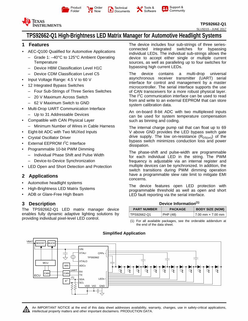
CAN VDD VIO GND TX RX SDA SCL E 2 UART I 2 C LEDx VIN XTALI XTALO CAN MCU BUCK BOOST ECU VBAT TPS92662 BIN ADCx CPPx Product Folder Order Now Technical Documents Tools & Software Support & Community An IMPORTANT NOTICE at the end of this data sheet addresses availability, warranty, changes, use in safety-critical applications, intellectual property matters and other important disclaimers. PRODUCTION DATA. TPS92662-Q1 SLUSD15 – JUNE 2017 TPS92662-Q1 High-Brightness LED Matrix Manager for Automotive Headlight Systems 1 1 Features 1• AEC-Q100 Qualified for Automotive Applications – Grade 1: –40°C to 125°C Ambient Operating Temperature – Device HBM Classification Level H1C – Device CDM Classification Level C5 • Input Voltage Range: 4.5 V to 60 V • 12 Integrated Bypass Switches – Four Sub-Strings of Three Series Switches – 20 V Maximum Across Switch – 62 V Maximum Switch to GND • Multi-Drop UART Communication Interface – Up to 31 Addressable Devices • Compatible with CAN Physical Layer – Minimum Number of Wires in Cable Harness • Eight-bit ADC with Two MUXed Inputs • Crystal Oscillator Driver • External EEPROM I 2 C Interface • Programmable 10-bit PWM Dimming – Individual Phase Shift and Pulse Width – Device-to-Device Synchronization • LED Open and Short Detection and Protection 2 Applications • Automotive headlight systems • High-Brightness LED Matrix Systems • ADB or Glare-Free High Beam 3 Description The TPS92662-Q1 LED matrix manager device enables fully dynamic adaptive lighting solutions by providing individual pixel-level LED control. The device includes four sub-strings of three series- connected integrated switches for bypassing individual LEDs. The individual sub-strings allows the device to accept either single or multiple current sources, as well as paralleling up to four switches for bypassing high current LEDs. The device contains a multi-drop universal asynchronous receiver transmitter (UART) serial interface for control and management by a master microcontroller. The serial interface supports the use of CAN transceivers for a more robust physical layer. The I 2 C communication interface can be used to read from and write to an external EEPROM that can store system calibration data. An on-board 8-bit ADC with two multiplexed inputs can be used for system temperature compensation such as binning and coding. The internal charge pump rail that can float up to 69 V above GND provides the LED bypass switch gate drive supply. The low on-resistance (R DS(on) ) of the bypass switch minimizes conduction loss and power dissipation. The phase-shift and pulse-width are programmable for each individual LED in the string. The PWM frequency is adjustable via an internal register and multiple devices can be synchronized. In addition, the switch transitions during PWM dimming operation have a programmable slew rate limit to mitigate EMI concerns. The device features open LED protection with programmable threshold as well as open and short LED fault reporting via the serial interface. Device Information (1) PART NUMBER PACKAGE BODY SIZE (NOM) TPS92662-Q1 PHP (48) 7.00 mm × 7.00 mm (1) For all available packages, see the orderable addendum at the end of the data sheet. Simplified Application
Transcript of TPS92662-Q1 High-Brightness LED Matrix Manager for ... · PACKAGE OPTION ADDENDUM 16-Jun-2017...
CAN
VDD VIO GND
TXRX
SDASCL
E2
UART
I2C LEDx
VIN
XTALI
XTALO
CAN
MCU
BUCKBOOST
ECU
VBAT
TPS92662
BIN ADCx
CPPx
Product
Folder
Order
Now
Technical
Documents
Tools &
Software
Support &Community
An IMPORTANT NOTICE at the end of this data sheet addresses availability, warranty, changes, use in safety-critical applications,intellectual property matters and other important disclaimers. PRODUCTION DATA.
TPS92662-Q1SLUSD15 –JUNE 2017
TPS92662-Q1 High-Brightness LED Matrix Manager for Automotive Headlight Systems
1
1 Features1• AEC-Q100 Qualified for Automotive Applications
– Grade 1: –40°C to 125°C Ambient OperatingTemperature
– Device HBM Classification Level H1C– Device CDM Classification Level C5
• Input Voltage Range: 4.5 V to 60 V• 12 Integrated Bypass Switches
– Four Sub-Strings of Three Series Switches– 20 V Maximum Across Switch– 62 V Maximum Switch to GND
• Multi-Drop UART Communication Interface– Up to 31 Addressable Devices
• Compatible with CAN Physical Layer– Minimum Number of Wires in Cable Harness
• Eight-bit ADC with Two MUXed Inputs• Crystal Oscillator Driver• External EEPROM I2C Interface• Programmable 10-bit PWM Dimming
– Individual Phase Shift and Pulse Width– Device-to-Device Synchronization
• LED Open and Short Detection and Protection
2 Applications• Automotive headlight systems• High-Brightness LED Matrix Systems• ADB or Glare-Free High Beam
3 DescriptionThe TPS92662-Q1 LED matrix manager deviceenables fully dynamic adaptive lighting solutions byproviding individual pixel-level LED control.
The device includes four sub-strings of three series-connected integrated switches for bypassingindividual LEDs. The individual sub-strings allows thedevice to accept either single or multiple currentsources, as well as paralleling up to four switches forbypassing high current LEDs.
The device contains a multi-drop universalasynchronous receiver transmitter (UART) serialinterface for control and management by a mastermicrocontroller. The serial interface supports the useof CAN transceivers for a more robust physical layer.The I2C communication interface can be used to readfrom and write to an external EEPROM that can storesystem calibration data.
An on-board 8-bit ADC with two multiplexed inputscan be used for system temperature compensationsuch as binning and coding.
The internal charge pump rail that can float up to 69V above GND provides the LED bypass switch gatedrive supply. The low on-resistance (RDS(on)) of thebypass switch minimizes conduction loss and powerdissipation.
The phase-shift and pulse-width are programmablefor each individual LED in the string. The PWMfrequency is adjustable via an internal register andmultiple devices can be synchronized. In addition, theswitch transitions during PWM dimming operationhave a programmable slew rate limit to mitigate EMIconcerns.
The device features open LED protection withprogrammable threshold as well as open and shortLED fault reporting via the serial interface.
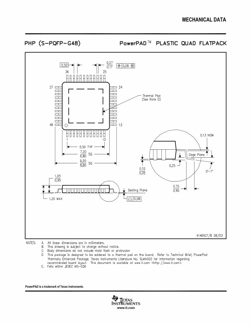
Device Information(1)
PART NUMBER PACKAGE BODY SIZE (NOM)TPS92662-Q1 PHP (48) 7.00 mm × 7.00 mm
(1) For all available packages, see the orderable addendum atthe end of the data sheet.
Simplified Application
2
TPS92662-Q1SLUSD15 –JUNE 2017 www.ti.com
Product Folder Links: TPS92662-Q1
Submit Documentation Feedback Copyright © 2017, Texas Instruments Incorporated
Table of Contents1 Features .................................................................. 12 Applications ........................................................... 13 Description ............................................................. 14 Revision History..................................................... 25 Device and Documentation Support.................... 3
5.1 Receiving Notification of Documentation Updates.... 3
5.2 Community Resources.............................................. 35.3 Trademarks ............................................................... 35.4 Electrostatic Discharge Caution................................ 35.5 Glossary .................................................................... 3
6 Mechanical, Packaging, and OrderableInformation ............................................................. 4
4 Revision HistoryNOTE: Page numbers for previous revisions may differ from page numbers in the current version.
DATE REVISION NOTESJune 2017 * Initial release.
3
TPS92662-Q1www.ti.com SLUSD15 –JUNE 2017
Product Folder Links: TPS92662-Q1
Submit Documentation FeedbackCopyright © 2017, Texas Instruments Incorporated
5 Device and Documentation Support
5.1 Receiving Notification of Documentation UpdatesTo receive notification of documentation updates, navigate to the device product folder on ti.com. In the upperright corner, click on Alert me to register and receive a weekly digest of any product information that haschanged. For change details, review the revision history included in any revised document.
5.2 Community ResourcesThe following links connect to TI community resources. Linked contents are provided "AS IS" by the respectivecontributors. They do not constitute TI specifications and do not necessarily reflect TI's views; see TI's Terms ofUse.
TI E2E™ Online Community TI's Engineer-to-Engineer (E2E) Community. Created to foster collaborationamong engineers. At e2e.ti.com, you can ask questions, share knowledge, explore ideas and helpsolve problems with fellow engineers.
Design Support TI's Design Support Quickly find helpful E2E forums along with design support tools andcontact information for technical support.
5.3 TrademarksE2E is a trademark of Texas Instruments.All other trademarks are the property of their respective owners.
5.4 Electrostatic Discharge CautionThis integrated circuit can be damaged by ESD. Texas Instruments recommends that all integrated circuits be handled withappropriate precautions. Failure to observe proper handling and installation procedures can cause damage.
ESD damage can range from subtle performance degradation to complete device failure. Precision integrated circuits may be moresusceptible to damage because very small parametric changes could cause the device not to meet its published specifications.
5.5 GlossarySLYZ022 — TI Glossary.
This glossary lists and explains terms, acronyms, and definitions.
4
TPS92662-Q1SLUSD15 –JUNE 2017 www.ti.com
Product Folder Links: TPS92662-Q1
Submit Documentation Feedback Copyright © 2017, Texas Instruments Incorporated
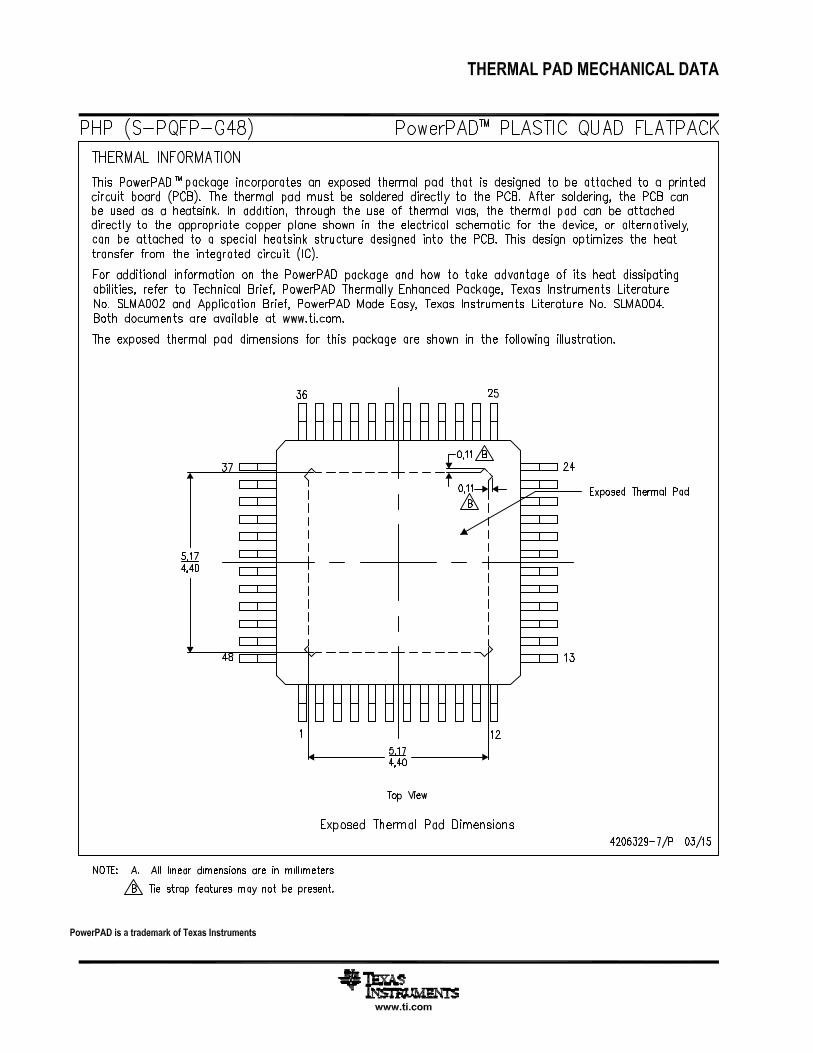
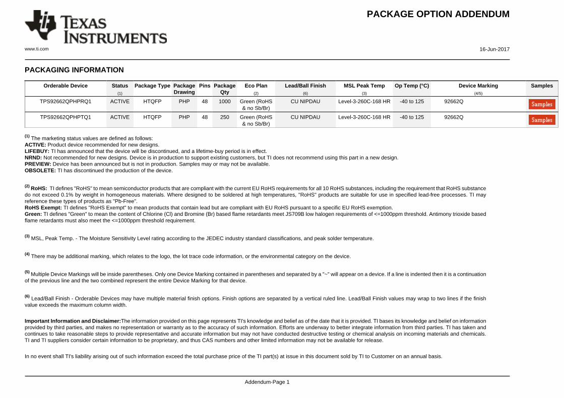
6 Mechanical, Packaging, and Orderable InformationThe following pages include mechanical, packaging, and orderable information. This information is the mostcurrent data available for the designated devices. This data is subject to change without notice and revision ofthis document. For browser-based versions of this data sheet, refer to the left-hand navigation.
PACKAGE OPTION ADDENDUM
www.ti.com 16-Jun-2017
Addendum-Page 1
PACKAGING INFORMATION
Orderable Device Status(1)
Package Type PackageDrawing
Pins PackageQty
Eco Plan(2)
Lead/Ball Finish(6)
MSL Peak Temp(3)
Op Temp (°C) Device Marking(4/5)
Samples
TPS92662QPHPRQ1 ACTIVE HTQFP PHP 48 1000 Green (RoHS& no Sb/Br)
CU NIPDAU Level-3-260C-168 HR -40 to 125 92662Q
TPS92662QPHPTQ1 ACTIVE HTQFP PHP 48 250 Green (RoHS& no Sb/Br)
CU NIPDAU Level-3-260C-168 HR -40 to 125 92662Q
(1) The marketing status values are defined as follows:ACTIVE: Product device recommended for new designs.LIFEBUY: TI has announced that the device will be discontinued, and a lifetime-buy period is in effect.NRND: Not recommended for new designs. Device is in production to support existing customers, but TI does not recommend using this part in a new design.PREVIEW: Device has been announced but is not in production. Samples may or may not be available.OBSOLETE: TI has discontinued the production of the device.
(2) RoHS: TI defines "RoHS" to mean semiconductor products that are compliant with the current EU RoHS requirements for all 10 RoHS substances, including the requirement that RoHS substancedo not exceed 0.1% by weight in homogeneous materials. Where designed to be soldered at high temperatures, "RoHS" products are suitable for use in specified lead-free processes. TI mayreference these types of products as "Pb-Free".RoHS Exempt: TI defines "RoHS Exempt" to mean products that contain lead but are compliant with EU RoHS pursuant to a specific EU RoHS exemption.Green: TI defines "Green" to mean the content of Chlorine (Cl) and Bromine (Br) based flame retardants meet JS709B low halogen requirements of <=1000ppm threshold. Antimony trioxide basedflame retardants must also meet the <=1000ppm threshold requirement.
(3) MSL, Peak Temp. - The Moisture Sensitivity Level rating according to the JEDEC industry standard classifications, and peak solder temperature.
(4) There may be additional marking, which relates to the logo, the lot trace code information, or the environmental category on the device.
(5) Multiple Device Markings will be inside parentheses. Only one Device Marking contained in parentheses and separated by a "~" will appear on a device. If a line is indented then it is a continuationof the previous line and the two combined represent the entire Device Marking for that device.
(6) Lead/Ball Finish - Orderable Devices may have multiple material finish options. Finish options are separated by a vertical ruled line. Lead/Ball Finish values may wrap to two lines if the finishvalue exceeds the maximum column width.
Important Information and Disclaimer:The information provided on this page represents TI's knowledge and belief as of the date that it is provided. TI bases its knowledge and belief on informationprovided by third parties, and makes no representation or warranty as to the accuracy of such information. Efforts are underway to better integrate information from third parties. TI has taken andcontinues to take reasonable steps to provide representative and accurate information but may not have conducted destructive testing or chemical analysis on incoming materials and chemicals.TI and TI suppliers consider certain information to be proprietary, and thus CAS numbers and other limited information may not be available for release.
In no event shall TI's liability arising out of such information exceed the total purchase price of the TI part(s) at issue in this document sold by TI to Customer on an annual basis.
PACKAGE OPTION ADDENDUM
www.ti.com 16-Jun-2017
Addendum-Page 2
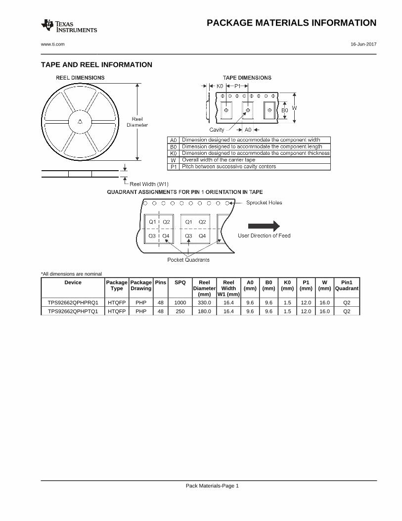
TAPE AND REEL INFORMATION
*All dimensions are nominal
Device PackageType
PackageDrawing
Pins SPQ ReelDiameter
(mm)
ReelWidth
W1 (mm)
A0(mm)
B0(mm)
K0(mm)
P1(mm)
W(mm)
Pin1Quadrant
TPS92662QPHPRQ1 HTQFP PHP 48 1000 330.0 16.4 9.6 9.6 1.5 12.0 16.0 Q2
TPS92662QPHPTQ1 HTQFP PHP 48 250 180.0 16.4 9.6 9.6 1.5 12.0 16.0 Q2
PACKAGE MATERIALS INFORMATION
www.ti.com 16-Jun-2017
Pack Materials-Page 1
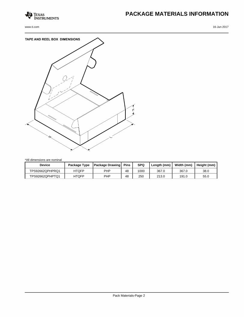
*All dimensions are nominal
Device Package Type Package Drawing Pins SPQ Length (mm) Width (mm) Height (mm)
TPS92662QPHPRQ1 HTQFP PHP 48 1000 367.0 367.0 38.0
TPS92662QPHPTQ1 HTQFP PHP 48 250 213.0 191.0 55.0
PACKAGE MATERIALS INFORMATION
www.ti.com 16-Jun-2017
Pack Materials-Page 2

IMPORTANT NOTICE
Texas Instruments Incorporated (TI) reserves the right to make corrections, enhancements, improvements and other changes to itssemiconductor products and services per JESD46, latest issue, and to discontinue any product or service per JESD48, latest issue. Buyersshould obtain the latest relevant information before placing orders and should verify that such information is current and complete.TI’s published terms of sale for semiconductor products (http://www.ti.com/sc/docs/stdterms.htm) apply to the sale of packaged integratedcircuit products that TI has qualified and released to market. Additional terms may apply to the use or sale of other types of TI products andservices.Reproduction of significant portions of TI information in TI data sheets is permissible only if reproduction is without alteration and isaccompanied by all associated warranties, conditions, limitations, and notices. TI is not responsible or liable for such reproduceddocumentation. Information of third parties may be subject to additional restrictions. Resale of TI products or services with statementsdifferent from or beyond the parameters stated by TI for that product or service voids all express and any implied warranties for theassociated TI product or service and is an unfair and deceptive business practice. TI is not responsible or liable for any such statements.Buyers and others who are developing systems that incorporate TI products (collectively, “Designers”) understand and agree that Designersremain responsible for using their independent analysis, evaluation and judgment in designing their applications and that Designers havefull and exclusive responsibility to assure the safety of Designers' applications and compliance of their applications (and of all TI productsused in or for Designers’ applications) with all applicable regulations, laws and other applicable requirements. Designer represents that, withrespect to their applications, Designer has all the necessary expertise to create and implement safeguards that (1) anticipate dangerousconsequences of failures, (2) monitor failures and their consequences, and (3) lessen the likelihood of failures that might cause harm andtake appropriate actions. Designer agrees that prior to using or distributing any applications that include TI products, Designer willthoroughly test such applications and the functionality of such TI products as used in such applications.TI’s provision of technical, application or other design advice, quality characterization, reliability data or other services or information,including, but not limited to, reference designs and materials relating to evaluation modules, (collectively, “TI Resources”) are intended toassist designers who are developing applications that incorporate TI products; by downloading, accessing or using TI Resources in anyway, Designer (individually or, if Designer is acting on behalf of a company, Designer’s company) agrees to use any particular TI Resourcesolely for this purpose and subject to the terms of this Notice.TI’s provision of TI Resources does not expand or otherwise alter TI’s applicable published warranties or warranty disclaimers for TIproducts, and no additional obligations or liabilities arise from TI providing such TI Resources. TI reserves the right to make corrections,enhancements, improvements and other changes to its TI Resources. TI has not conducted any testing other than that specificallydescribed in the published documentation for a particular TI Resource.Designer is authorized to use, copy and modify any individual TI Resource only in connection with the development of applications thatinclude the TI product(s) identified in such TI Resource. NO OTHER LICENSE, EXPRESS OR IMPLIED, BY ESTOPPEL OR OTHERWISETO ANY OTHER TI INTELLECTUAL PROPERTY RIGHT, AND NO LICENSE TO ANY TECHNOLOGY OR INTELLECTUAL PROPERTYRIGHT OF TI OR ANY THIRD PARTY IS GRANTED HEREIN, including but not limited to any patent right, copyright, mask work right, orother intellectual property right relating to any combination, machine, or process in which TI products or services are used. Informationregarding or referencing third-party products or services does not constitute a license to use such products or services, or a warranty orendorsement thereof. Use of TI Resources may require a license from a third party under the patents or other intellectual property of thethird party, or a license from TI under the patents or other intellectual property of TI.TI RESOURCES ARE PROVIDED “AS IS” AND WITH ALL FAULTS. TI DISCLAIMS ALL OTHER WARRANTIES ORREPRESENTATIONS, EXPRESS OR IMPLIED, REGARDING RESOURCES OR USE THEREOF, INCLUDING BUT NOT LIMITED TOACCURACY OR COMPLETENESS, TITLE, ANY EPIDEMIC FAILURE WARRANTY AND ANY IMPLIED WARRANTIES OFMERCHANTABILITY, FITNESS FOR A PARTICULAR PURPOSE, AND NON-INFRINGEMENT OF ANY THIRD PARTY INTELLECTUALPROPERTY RIGHTS. TI SHALL NOT BE LIABLE FOR AND SHALL NOT DEFEND OR INDEMNIFY DESIGNER AGAINST ANY CLAIM,INCLUDING BUT NOT LIMITED TO ANY INFRINGEMENT CLAIM THAT RELATES TO OR IS BASED ON ANY COMBINATION OFPRODUCTS EVEN IF DESCRIBED IN TI RESOURCES OR OTHERWISE. IN NO EVENT SHALL TI BE LIABLE FOR ANY ACTUAL,DIRECT, SPECIAL, COLLATERAL, INDIRECT, PUNITIVE, INCIDENTAL, CONSEQUENTIAL OR EXEMPLARY DAMAGES INCONNECTION WITH OR ARISING OUT OF TI RESOURCES OR USE THEREOF, AND REGARDLESS OF WHETHER TI HAS BEENADVISED OF THE POSSIBILITY OF SUCH DAMAGES.Unless TI has explicitly designated an individual product as meeting the requirements of a particular industry standard (e.g., ISO/TS 16949and ISO 26262), TI is not responsible for any failure to meet such industry standard requirements.Where TI specifically promotes products as facilitating functional safety or as compliant with industry functional safety standards, suchproducts are intended to help enable customers to design and create their own applications that meet applicable functional safety standardsand requirements. Using products in an application does not by itself establish any safety features in the application. Designers mustensure compliance with safety-related requirements and standards applicable to their applications. Designer may not use any TI products inlife-critical medical equipment unless authorized officers of the parties have executed a special contract specifically governing such use.Life-critical medical equipment is medical equipment where failure of such equipment would cause serious bodily injury or death (e.g., lifesupport, pacemakers, defibrillators, heart pumps, neurostimulators, and implantables). Such equipment includes, without limitation, allmedical devices identified by the U.S. Food and Drug Administration as Class III devices and equivalent classifications outside the U.S.TI may expressly designate certain products as completing a particular qualification (e.g., Q100, Military Grade, or Enhanced Product).Designers agree that it has the necessary expertise to select the product with the appropriate qualification designation for their applicationsand that proper product selection is at Designers’ own risk. Designers are solely responsible for compliance with all legal and regulatoryrequirements in connection with such selection.Designer will fully indemnify TI and its representatives against any damages, costs, losses, and/or liabilities arising out of Designer’s non-compliance with the terms and provisions of this Notice.
Mailing Address: Texas Instruments, Post Office Box 655303, Dallas, Texas 75265Copyright © 2017, Texas Instruments Incorporated