SLVSDO5B –JULY 2017–REVISED DECEMBER 2017 … · PACKAGE OPTION ADDENDUM 6-Jun-2018...
29
L H TPS22916xx VIN VOUT RL CL ON GND VIN + – CIN Copyright © 2017, Texas Instruments Incorporated Product Folder Order Now Technical Documents Tools & Software Support & Community An IMPORTANT NOTICE at the end of this data sheet addresses availability, warranty, changes, use in safety-critical applications, intellectual property matters and other important disclaimers. PRODUCTION DATA. TPS22916 SLVSDO5B – JULY 2017 – REVISED DECEMBER 2017 TPS22916xx 1-V – 5.5-V, 2-A, 60-mΩ Ultra-Low Leakage Load Switch 1 1 Features 1• Input Operating Voltage Range (V IN ): 1 V–5.5 V • Maximum Continuous Current (I MAX ): 2 A • ON-Resistance (R ON ): – 5V IN = 60 mΩ (typ), 100 mΩ (85°C max) – 1.8 V IN = 100 mΩ (typ), 150 mΩ (85°C max) – 1V IN = 200 mΩ (typ), 325 mΩ (85°C max) • Ultra-Low Power Consumption: – ON State (I Q ): 0.5 μA (typ), 1 μA (max) – OFF State (I SD ): 10 nA (typ), 100 nA (max) – TPS22916CL (I SD ): 100 nA (typ), 300 nA (max) • Smart ON Pin Pull Down (R PD ): – ON ≥ V IH (I ON ): 10 nA (max) – ON ≤ V IL (R PD ): 750 kΩ (typ) • Slow Timing in C Version Limits Inrush Current: – 5-V Turnon time (t ON ): 1400 μs at 5 mV/μs – 1.8-V Turnon time (t ON ): 3000 μs at 1 mV/μs – 1-V Turnon time (t ON ): 6500 μs at 0.3 mV/μs • Fast Timing in B Version Reduces Wait Time: – 5-V Turnon time (t ON ): 115 μs at 57 mV/μs – 1.8-V Turnon time (t ON ): 250 μs at 12 mV/μs – 1-V Turnon time (t ON ): 510 μs at 3.3 mV/μs • Always-ON True Reverse Current Blocking (RCB): – Activation Current (I RCB ): –500 mA (typ) – Reverse Leakage (I IN,RCB ): –300 nA (max) • Quick Output Discharge (QOD): 150 Ω (typ) (N version has no QOD) • Active Low Enable Option (L Version) 2 Applications • Wearables • Smartphones • Tablets • Portable Speakers 3 Description The TPS22916xx is a small, single channel load switch using a low leakage P-Channel MOSFET for minimum power loss. Advanced gate control design supports operating voltages as low as 1 V with minimal increase in ON-Resistance and power loss. Multiple timing options are available to support various system loading conditions. For heavy capacitive loads, the slow turnon timing in the C version minimizes the inrush current. In cases with light capacitive loads, the fast timing in the B version reduces required wait time. The switch ON state is controlled by a digital input that is capable of interfacing directly with low-voltage control signals. Both Active High and Active Low (L) versions are available. When power is first applied, a Smart Pull Down is used to keep the ON pin from floating until system sequencing is complete. Once the ON pin is deliberately driven high (≥V IH ), the Smart Pull Down is disconnected to prevent unnecessary power loss. The TPS22916xx is available in a small, space saving 0.74-mm × 0.74-mm, 0.4-mm pitch, 0.5-mm height 4-pin Wafer-Chip-Scale (WCSP) package (YFP). The device is characterized for operation over a temperature range of –40°C to +85°C. Device Information (1) PART NUMBER PACKAGE BODY SIZE (NOM) TPS22916xx WCSP (4) 0.74 mm × 0.74 mm (1) For all available packages, see the orderable addendum at the end of the data sheet. Device Comparison Table VERSION TIMING QOD ENABLE (ON) TPS22916B Fast Yes Active High TPS22916C Slow Yes Active High TPS22916CN Slow No Active High TPS22916CL Slow Yes Active Low Simplified Schematic
Transcript of SLVSDO5B –JULY 2017–REVISED DECEMBER 2017 … · PACKAGE OPTION ADDENDUM 6-Jun-2018...

L
H
TPS22916xx
VIN VOUT
RLCL
ON GND
VIN+
±
CIN
Copyright © 2017, Texas Instruments Incorporated
Product
Folder
Order
Now
Technical
Documents
Tools &
Software
Support &Community
An IMPORTANT NOTICE at the end of this data sheet addresses availability, warranty, changes, use in safety-critical applications,intellectual property matters and other important disclaimers. PRODUCTION DATA.
TPS22916SLVSDO5B –JULY 2017–REVISED DECEMBER 2017
TPS22916xx 1-V – 5.5-V, 2-A, 60-mΩ Ultra-Low Leakage Load Switch
1
1 Features1• Input Operating Voltage Range (VIN): 1 V–5.5 V• Maximum Continuous Current (IMAX): 2 A• ON-Resistance (RON):
– 5 VIN = 60 mΩ (typ), 100 mΩ (85°C max)– 1.8 VIN = 100 mΩ (typ), 150 mΩ (85°C max)– 1 VIN = 200 mΩ (typ), 325 mΩ (85°C max)
• Ultra-Low Power Consumption:– ON State (IQ): 0.5 µA (typ), 1 µA (max)– OFF State (ISD): 10 nA (typ), 100 nA (max)– TPS22916CL (ISD): 100 nA (typ), 300 nA (max)
• Smart ON Pin Pull Down (RPD):– ON ≥ VIH (ION): 10 nA (max)– ON ≤ VIL (RPD): 750 kΩ (typ)
• Slow Timing in C Version Limits Inrush Current:– 5-V Turnon time (tON): 1400 µs at 5 mV/µs– 1.8-V Turnon time (tON): 3000 µs at 1 mV/µs– 1-V Turnon time (tON): 6500 µs at 0.3 mV/µs
• Fast Timing in B Version Reduces Wait Time:– 5-V Turnon time (tON): 115 µs at 57 mV/µs– 1.8-V Turnon time (tON): 250 µs at 12 mV/µs– 1-V Turnon time (tON): 510 µs at 3.3 mV/µs
• Always-ON True Reverse Current Blocking (RCB):– Activation Current (IRCB): –500 mA (typ)– Reverse Leakage (IIN,RCB): –300 nA (max)
• Quick Output Discharge (QOD): 150 Ω (typ)(N version has no QOD)
• Active Low Enable Option (L Version)
2 Applications• Wearables• Smartphones• Tablets• Portable Speakers
3 DescriptionThe TPS22916xx is a small, single channel loadswitch using a low leakage P-Channel MOSFET forminimum power loss. Advanced gate control designsupports operating voltages as low as 1 V withminimal increase in ON-Resistance and power loss.
Multiple timing options are available to supportvarious system loading conditions. For heavycapacitive loads, the slow turnon timing in the Cversion minimizes the inrush current. In cases withlight capacitive loads, the fast timing in the B versionreduces required wait time.
The switch ON state is controlled by a digital inputthat is capable of interfacing directly with low-voltagecontrol signals. Both Active High and Active Low (L)versions are available. When power is first applied, aSmart Pull Down is used to keep the ON pin fromfloating until system sequencing is complete. Oncethe ON pin is deliberately driven high (≥VIH), theSmart Pull Down is disconnected to preventunnecessary power loss.
The TPS22916xx is available in a small, spacesaving 0.74-mm × 0.74-mm, 0.4-mm pitch, 0.5-mmheight 4-pin Wafer-Chip-Scale (WCSP) package(YFP). The device is characterized for operation overa temperature range of –40°C to +85°C.
Device Information(1)
PART NUMBER PACKAGE BODY SIZE (NOM)TPS22916xx WCSP (4) 0.74 mm × 0.74 mm
(1) For all available packages, see the orderable addendum atthe end of the data sheet.
Device Comparison TableVERSION TIMING QOD ENABLE (ON)
TPS22916B Fast Yes Active HighTPS22916C Slow Yes Active HighTPS22916CN Slow No Active HighTPS22916CL Slow Yes Active Low
Simplified Schematic
2
TPS22916SLVSDO5B –JULY 2017–REVISED DECEMBER 2017 www.ti.com
Product Folder Links: TPS22916
Submit Documentation Feedback Copyright © 2017, Texas Instruments Incorporated
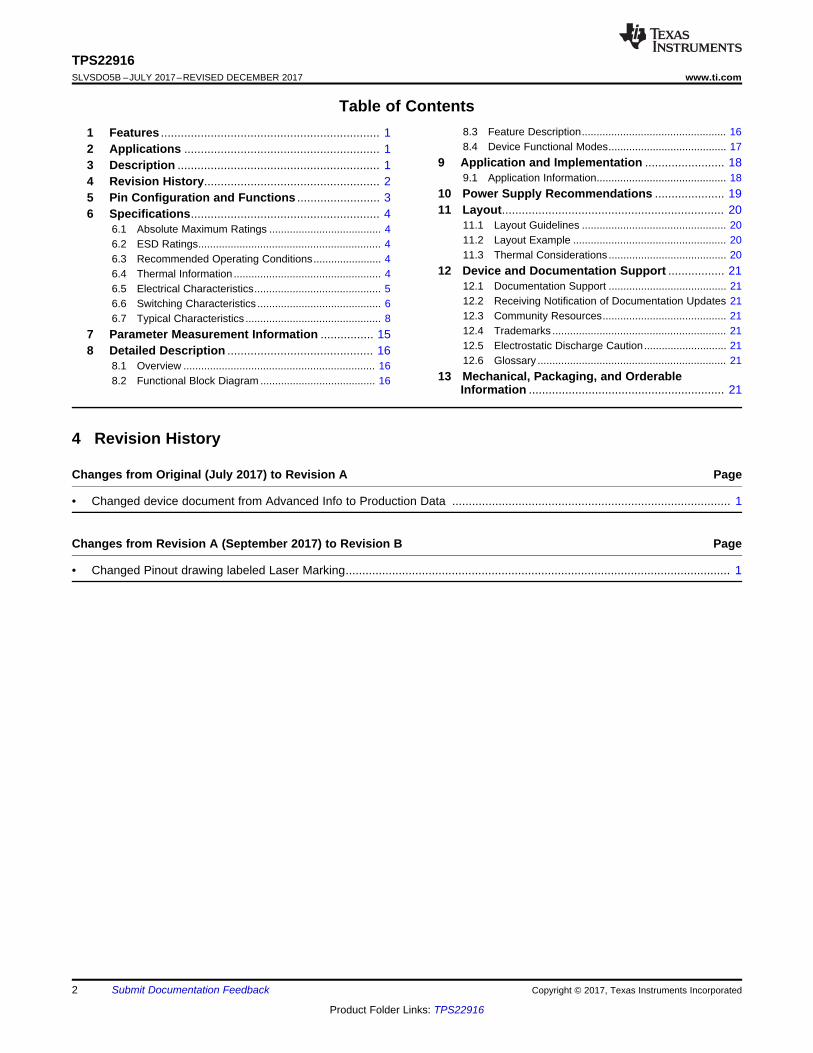
Table of Contents1 Features .................................................................. 12 Applications ........................................................... 13 Description ............................................................. 14 Revision History..................................................... 25 Pin Configuration and Functions ......................... 36 Specifications......................................................... 4
6.1 Absolute Maximum Ratings ...................................... 46.2 ESD Ratings.............................................................. 46.3 Recommended Operating Conditions....................... 46.4 Thermal Information .................................................. 46.5 Electrical Characteristics........................................... 56.6 Switching Characteristics .......................................... 66.7 Typical Characteristics .............................................. 8
7 Parameter Measurement Information ................ 158 Detailed Description ............................................ 16
8.1 Overview ................................................................. 168.2 Functional Block Diagram ....................................... 16
8.3 Feature Description................................................. 168.4 Device Functional Modes........................................ 17
9 Application and Implementation ........................ 189.1 Application Information............................................ 18
10 Power Supply Recommendations ..................... 1911 Layout................................................................... 20
11.1 Layout Guidelines ................................................. 2011.2 Layout Example .................................................... 2011.3 Thermal Considerations ........................................ 20
12 Device and Documentation Support ................. 2112.1 Documentation Support ........................................ 2112.2 Receiving Notification of Documentation Updates 2112.3 Community Resources.......................................... 2112.4 Trademarks ........................................................... 2112.5 Electrostatic Discharge Caution............................ 2112.6 Glossary ................................................................ 21
13 Mechanical, Packaging, and OrderableInformation ........................................................... 21
4 Revision History
Changes from Original (July 2017) to Revision A Page
• Changed device document from Advanced Info to Production Data .................................................................................... 1
Changes from Revision A (September 2017) to Revision B Page
• Changed Pinout drawing labeled Laser Marking.................................................................................................................... 1

B
A
21
VOUT
GND ON
VIN
B
A
12
VIN
ON GND
VOUT
3
TPS22916www.ti.com SLVSDO5B –JULY 2017–REVISED DECEMBER 2017
Product Folder Links: TPS22916
Submit Documentation FeedbackCopyright © 2017, Texas Instruments Incorporated
5 Pin Configuration and Functions
YFP Package4-Pin WSON
Laser Marking View
YFP Package4-Pin WSONBump View
TPS22916xx Pin FunctionsPIN
TYPE DESCRIPTIONNO. NAMEA1 VOUT Power Switch outputA2 VIN Power Switch inputB1 GND Ground Device groundB2 ON Digital input Device enable

4
TPS22916SLVSDO5B –JULY 2017–REVISED DECEMBER 2017 www.ti.com
Product Folder Links: TPS22916
Submit Documentation Feedback Copyright © 2017, Texas Instruments Incorporated
(1) Stresses beyond those listed under Absolute Maximum Ratings may cause permanent damage to the device. These are stress ratingsonly, which do not imply functional operation of the device at these or any other conditions beyond those indicated under RecommendedOperating Conditions. Exposure to absolute-maximum-rated conditions for extended periods may affect device reliability.
6 Specifications
6.1 Absolute Maximum RatingsOver operating free-air temperature range (unless otherwise noted) (1)
MIN MAX UNITVIN Input voltage –0.3 6 VVOUT Output voltage –0.3 6 VVON Enable voltage –0.3 6 VIMAX Maximum continuous switch current 2 AIPLS Maximum pulsed switch current, pulse < 300-µs, 2% duty cycle 2.5 ATJ,MAX Maximum junction temperature 125 °CTSTG Storage temperature –65 150 °CTLEAD Maximum Lead temperature (10-s soldering time) 300 °C
(1) JEDEC document JEP155 states that 500-V HBM allows safe manufacturing with a standard ESD control process. Manufacturing withless than 500-V HBM is possible with the necessary precautions. Pins listed as ±2000 V may actually have higher performance.
(2) JEDEC document JEP157 states that 250-V CDM allows safe manufacturing with a standard ESD control process. Manufacturing withless than 250-V CDM is possible with the necessary precautions. Pins listed as ±500 V may actually have higher performance.
6.2 ESD RatingsVALUE UNIT
V(ESD) Electrostatic dischargeHuman-body model (HBM), per ANSI/ESDA/JEDEC JS-001 (1) ±2000
VCharged-device model (CDM), per JEDEC specification JESD22-C101 (2) ±500
6.3 Recommended Operating ConditionsOver operating free-air temperature range (unless otherwise noted)
MIN MAX UNITVIN Input voltage 1 5.5 VVOUT Output voltage 0 5.5 VVIH High-level input voltage, ON 1 5.5 VVIL Low-level input voltage, ON 0 0.35 VTA Operating free-air temperature –40 85 °C
(1) For more information about traditional and new thermal metrics, see the Semiconductor and IC Package Thermal Metrics applicationreport.
6.4 Thermal Information
Thermal Parameters (1)TPS22916xx
UNITYFP (WCSP)4 PINS
θJA Junction-to-ambient thermal resistance 193 °C/WθJCtop Junction-to-case (top) thermal resistance 2.3 °C/WθJB Junction-to-board thermal resistance 36 °C/WψJT Junction-to-top characterization parameter 12 °C/WψJB Junction-to-board characterization parameter 36 °C/W

5
TPS22916www.ti.com SLVSDO5B –JULY 2017–REVISED DECEMBER 2017
Product Folder Links: TPS22916
Submit Documentation FeedbackCopyright © 2017, Texas Instruments Incorporated
(1) For more information on which devices include quick output discharge, see the Device Functional Modes section.
6.5 Electrical CharacteristicsUnless otherwise noted, the specification in the following table applies for all variants over the entire recommended powersupply voltage range of 1 V to 5.5 V unless noted otherwise. Typical Values are at 25°C.
PARAMETER TEST CONDITIONS TJ MIN TYP MAX UNITINPUT SUPPLY (VIN)IQ,VIN VIN Quiescent current Enabled, VOUT = Open –40°C to +85°C 0.5 1.0 µAISD,VIN VIN Shutdown current Disabled, VOUT = GND (TPS22916B/C/CN) –40°C to +85°C 10 100 nA
Disabled, VOUT = GND (TPS22916CL) –40°C to +85°C 100 300 nAON-RESISTANCE(RON)
RON ON-Resistance IOUT = 200 mA
VIN = 5 V25°C 60 80
mΩ
–40°C to +85°C 100–40°C to +105°C 120
VIN = 3.6 V25°C 70 90–40°C to +85°C 120–40°C to +105°C 140
VIN = 1.8 V25°C 100 125–40°C to +85°C 150–40°C to +105°C 175
VIN = 1.2 V25°C 150 200–40°C to +85°C 250–40°C to +105°C 300
VIN = 1 V25°C 200 275–40°C to +85°C 325–40°C to +105°C 375
ENABLE PIN (ON)ION ON Pin leakage Enabled –40°C to +85°C –10 10 nARPD Smart Pull Down Resistance Disabled –40°C to +85°C 750 kΩREVERSE CURRENT BLOCKING(RCB)IRCB RCB Activation Current Enabled, VOUT > VIN –40°C to +85°C -500 mAtRCB RCB Activation time Enabled, VOUT > VIN + 200mV –40°C to +85°C 10 µsVRCB RCB Release Voltage Enabled, VOUT > VIN –40°C to +85°C 25 mVIIN,RCB VIN Reverse Leakage Current 0 V ≤ VIN + VRCB ≤ VOUT ≤ 5.5 V –40°C to +85°C –300 nAQUICK OUTPUT DISCHARGE(QOD)QOD (1) Output discharge resistance Disabled (Not in TPS22916CN) –40°C to +85°C 150 Ω

6
TPS22916SLVSDO5B –JULY 2017–REVISED DECEMBER 2017 www.ti.com
Product Folder Links: TPS22916
Submit Documentation Feedback Copyright © 2017, Texas Instruments Incorporated
(1) See the Fall Time (tFALL) and Quick Output Discharge (QOD) section for information on how RL and CL affect Fall Time.
6.6 Switching CharacteristicsUnless otherwise noted, the typical characteristics in the following table applies over the entire recommended power supplyvoltage range of 1 V to 5.5 V at 25°C with a load of CL = 0.1µF, RL = 10Ω.
PARAMETER TEST CONDITIONS MIN TYP MAX UNITTPS22916B
tON Turn On Time
VIN = 5 V 115
µsVIN = 3.6 V 140VIN = 1.8 V 250VIN = 1.2 V 350VIN = 1 V 510
tRISE Rise Time
VIN = 5 V 70
µsVIN = 3.6 V 80VIN = 1.8 V 130VIN = 1.2 V 190VIN = 1 V 240
SRON Slew Rate
VIN = 5 V 57
mV/µsVIN = 3.6 V 36VIN = 1.8 V 12VIN = 1.2 V 5.1VIN = 1 V 3.3
tOFF Turn Off Time
VIN = 5 V 5
µsVIN = 3.6 V 5VIN = 1.8 V 10VIN = 1.2 V 15VIN = 1 V 25
tFALL Fall TimeCL = 0.1 µF, RL = 10 Ω (1) 2.3
µsCL = 1µF, RL = Open (1) 315

7
TPS22916www.ti.com SLVSDO5B –JULY 2017–REVISED DECEMBER 2017
Product Folder Links: TPS22916
Submit Documentation FeedbackCopyright © 2017, Texas Instruments Incorporated
Switching Characteristics (continued)Unless otherwise noted, the typical characteristics in the following table applies over the entire recommended power supplyvoltage range of 1 V to 5.5 V at 25°C with a load of CL = 0.1µF, RL = 10Ω.
PARAMETER TEST CONDITIONS MIN TYP MAX UNIT
(2) Devices without Quick Output Discharge (QOD) may not discharge completely.
TPS22916C, TPS22916CN, TPS22916CL
tON Turn On Time
VIN = 5 V 1400
µsVIN = 3.6 V 1700VIN = 1.8 V 3000VIN = 1.2 V 5000VIN = 1 V 6500
tRISE Rise Time
VIN = 5 V 800
µsVIN = 3.6 V 900VIN = 1.8 V 1400VIN = 1.2 V 2300VIN = 1 V 3000
SRON Slew Rate
VIN = 5 V 5
mV/µsVIN = 3.6 V 3.2VIN = 1.8 V 1VIN = 1.2 V 0.4VIN = 1 V 0.3
tOFF Turn Off Time
VIN = 5 V 5
µsVIN = 3.6 V 5VIN = 1.8 V 10VIN = 1.2 V 15VIN = 1 V 25
tFALL Fall Time (2) CL = 0.1 µF, RL = 10 Ω (1) 2.3µs
CL = 10µF, RL = Open (1) 3150

VIN (V)
I Q,V
IN (
nA)
1 1.5 2 2.5 3 3.5 4 4.5 5 5.5300
350
400
450
500
550
600
650
700
750
800
D001
85qC25qC40qC
VIN (V)
VO
N (
V)
1 1.5 2 2.5 3 3.5 4 4.5 5 5.50.54
0.56
0.58
0.6
0.62
0.64
0.66
0.68
0.7
0.72
D006
VIHVIL
VIN (V)
I SD
,VIN
(nA
)
1 1.5 2 2.5 3 3.5 4 4.5 5 5.50
5
10
15
20
25
30
35
40
45
50
D002
85qC25qC40qC
VIN (V)
I SD
,VIN
(nA
)
1 1.5 2 2.5 3 3.5 4 4.5 5 5.50
50
100
150
200
250
D015
85°C15°C40°C
Temperature (°C)
RO
N (
m:
)
-40 -20 0 20 40 60 80 100 12040
60
80
100
120
140
160
180
200
220
D004
1 V1.2 V1.8 V
3.6 V5 V
VIN (V)
RO
N (
m:
)
1 1.5 2 2.5 3 3.5 4 4.5 5 5.540
60
80
100
120
140
160
180
200
220
D003
105qC85qC25qC40qC
8
TPS22916SLVSDO5B –JULY 2017–REVISED DECEMBER 2017 www.ti.com
Product Folder Links: TPS22916
Submit Documentation Feedback Copyright © 2017, Texas Instruments Incorporated
6.7 Typical Characteristics
6.7.1 Typical Electrical CharacteristicsThe typical characteristics curves in this section apply to all devices unless otherwise noted.
Enabled
Figure 1. ON-Resistance vs Temperature
Enabled
Figure 2. ON-Resistance vs Input voltage
TPS22916C, TPS22916CN, TPS22916B VON ≤ VIL
Figure 3. Shutdown Current
TPS22916CL VON ≥ VIH
Figure 4. Shutdown Current (Active Low)
Enabled
Figure 5. Quiescent Current
–40°C to +85°C
Figure 6. ON Pin Threshold

Temperature (qC)
RP
D (
k:)
-40 -20 0 20 40 60 80 100650
700
750
800
850
900
950
1000
1050
D005VIN (V)
QO
D (:
)
1 1.5 2 2.5 3 3.5 4 4.5 5 5.5140
160
180
200
220
240
260
D007
85qC25qC40qC
9
TPS22916www.ti.com SLVSDO5B –JULY 2017–REVISED DECEMBER 2017
Product Folder Links: TPS22916
Submit Documentation FeedbackCopyright © 2017, Texas Instruments Incorporated
Typical Electrical Characteristics (continued)
VON ≤ VIL
Figure 7. ON Pin Smart Pull Down
TPS22916C TPS22916CL TPS22916B
Figure 8. Quick Output Discharge
VIN (V)
SR
ON (
mV
/Ps)
1 1.5 2 2.5 3 3.5 4 4.5 5 5.50
20
40
60
80
D008
85qC25qC40qC
VIN (V)
t RIS
E (P
s)
1 1.5 2 2.5 3 3.5 4 4.5 5 5.550
75
100
125
150
175
200
225
250
275
D010
85qC25qC40qC
VIN (V)
t ON (P
s)
1 1.5 2 2.5 3 3.5 4 4.5 5 5.5100
150
200
250
300
350
400
450
500
550
600
D009
85°C25°C40°C
10
TPS22916SLVSDO5B –JULY 2017–REVISED DECEMBER 2017 www.ti.com
Product Folder Links: TPS22916
Submit Documentation Feedback Copyright © 2017, Texas Instruments Incorporated
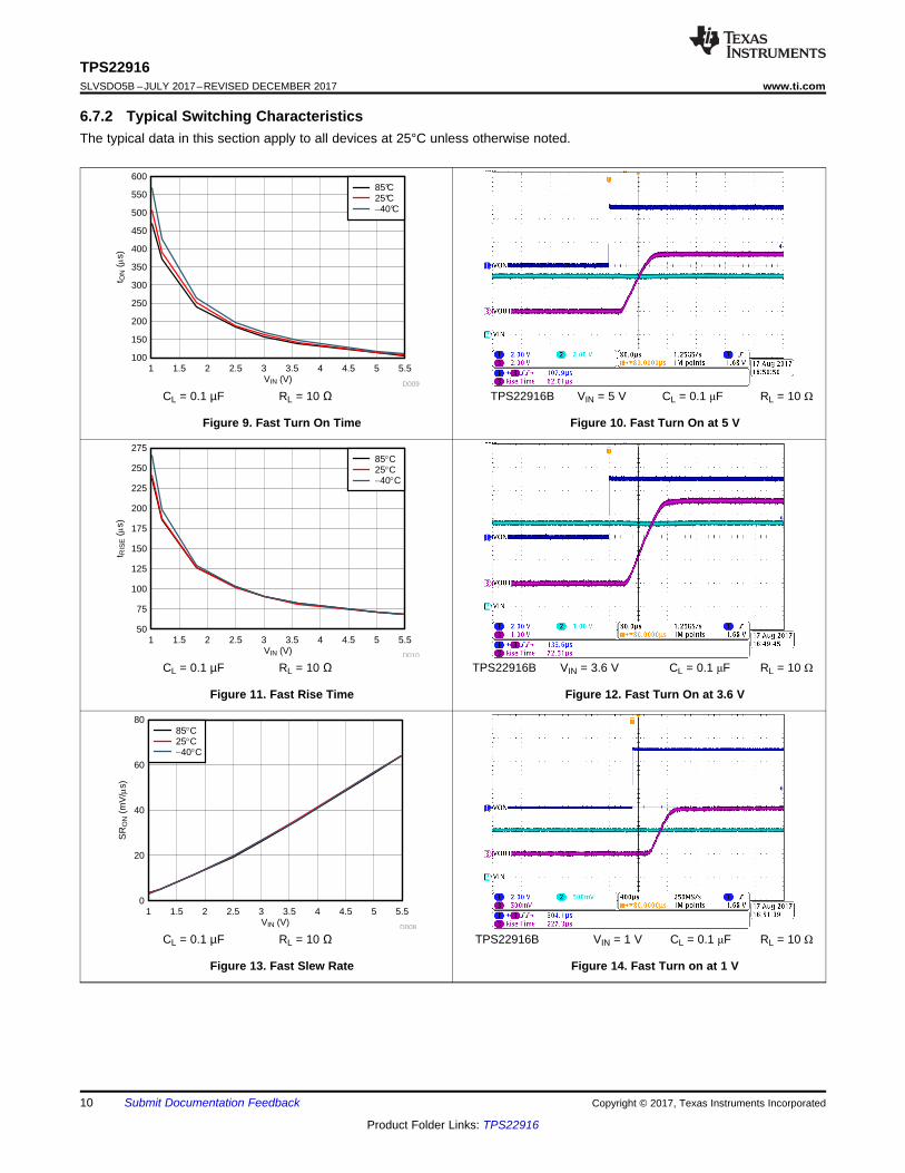
6.7.2 Typical Switching CharacteristicsThe typical data in this section apply to all devices at 25°C unless otherwise noted.
CL = 0.1 µF RL = 10 Ω
Figure 9. Fast Turn On Time
TPS22916B VIN = 5 V CL = 0.1 μF RL = 10 Ω
Figure 10. Fast Turn On at 5 V
CL = 0.1 µF RL = 10 Ω
Figure 11. Fast Rise Time
TPS22916B VIN = 3.6 V CL = 0.1 μF RL = 10 Ω
Figure 12. Fast Turn On at 3.6 V
CL = 0.1 µF RL = 10 Ω
Figure 13. Fast Slew Rate
TPS22916B VIN = 1 V CL = 0.1 μF RL = 10 Ω
Figure 14. Fast Turn on at 1 V

VIN (V)
SR
ON (
mV
/Ps)
1 1.5 2 2.5 3 3.5 4 4.5 5 5.50
20
40
60
80
D020
10 µF1 µF0.1 µF
VIN (V)
SR
ON (
mV
/Ps)
1 1.5 2 2.5 3 3.5 4 4.5 5 5.50
20
40
60
80
D021
3 :10 :Open
VIN (V)
t R (P
s)
1 1.5 2 2.5 3 3.5 4 4.5 5 5.560
90
120
150
180
210
240
270
D018
10 µF1 µF0.1 µF
VIN (V)
t R (P
s)
1 1.5 2 2.5 3 3.5 4 4.5 5 5.550
100
150
200
250
300
350
400
D019
3 :10 :Open
VIN (V)
t ON (P
s)
1 1.5 2 2.5 3 3.5 4 4.5 5 5.5100
150
200
250
300
350
400
450
500
550
D016
10 PF1 PF0.1 PF
VIN (V)
t ON (P
s)
1 1.5 2 2.5 3 3.5 4 4.5 5 5.5100
200
300
400
500
600
700
D017
3 :10 :Open
11
TPS22916www.ti.com SLVSDO5B –JULY 2017–REVISED DECEMBER 2017
Product Folder Links: TPS22916
Submit Documentation FeedbackCopyright © 2017, Texas Instruments Incorporated
Typical Switching Characteristics (continued)The typical data in this section apply to all devices at 25°C unless otherwise noted.
RL = 10 Ω TPS22916B
Figure 15. Fast Turn On vs Load Capacitance
CL = 10 µF TPS22916B
Figure 16. Fast Turn On vs Load Resistance
RL = 10 Ω TPS22916B
Figure 17. Fast Rise Time vs Load Capacitance
CL = 10 µF TPS22916B
Figure 18. Fast Rise Time vs Load Resistance
RL = 10 Ω TPS22916B
Figure 19. Fast Slew Rate vs Load Capacitance
CL = 10 µF TPS22916B
Figure 20. Fast Slew Rate vs Load Resistance

VIN (V)
SR
ON (
mV
/Ps)
1 1.5 2 2.5 3 3.5 4 4.5 5 5.50
1
2
3
4
5
6
D012
85qC25qC40qC
VIN (V)
t RIS
E (P
s)
1 1.5 2 2.5 3 3.5 4 4.5 5 5.5500
1000
1500
2000
2500
3000
3500
D014
85qC25qC40qC
VIN (V)
t ON (P
s)
1 1.5 2 2.5 3 3.5 4 4.5 5 5.50
1000
2000
3000
4000
5000
6000
7000
8000
D013
85qC25qC40qC
12
TPS22916SLVSDO5B –JULY 2017–REVISED DECEMBER 2017 www.ti.com
Product Folder Links: TPS22916
Submit Documentation Feedback Copyright © 2017, Texas Instruments Incorporated
Typical Switching Characteristics (continued)The typical data in this section apply to all devices at 25°C unless otherwise noted.
CL = 0.1 µF RL = 10 Ω
Figure 21. Slow Turn on Time
TPS22916C VIN = 5 V CL = 0.1 μF RL = 10 Ω
Figure 22. Slow Turn on at 5 V
CL = 0.1 µF RL = 10 Ω
Figure 23. Slow Rise Time
TPS22916C VIN = 3.6 V CL = 0.1 μF RL = 10 Ω
Figure 24. Slow Turn On at 3.6 V
CL = 0.1 µF RL = 10 Ω
Figure 25. Slow Slew Rate
TPS22916C VIN = 1 V CL = 0.1 μF RL = 10 Ω
Figure 26. Slow Turn On at 1 V

VIN (V)
SR
ON (
mV
/Ps)
1 1.5 2 2.5 3 3.5 4 4.5 5 5.50
1
2
3
4
5
6
D026
100 µF1 µF0.1 µF
VIN (V)
SR
ON (
mV
/Ps)
1 1.5 2 2.5 3 3.5 4 4.5 5 5.50
1
2
3
4
5
6
D027
3 :10 :Open
VIN (V)
t R (P
s)
1 1.5 2 2.5 3 3.5 4 4.5 5 5.5600
900
1200
1500
1800
2100
2400
2700
D024
100 µF1 µF0.1 µF
VIN (V)
t R (P
s)
1 1.5 2 2.5 3 3.5 4 4.5 5 5.5600
900
1200
1500
1800
2100
2400
2700
3000
3300
3600
D025
3 :10 :Open
VIN (V)
t ON (P
s)
1 1.5 2 2.5 3 3.5 4 4.5 5 5.51000
1500
2000
2500
3000
3500
4000
4500
5000
5500
6000
D022
100 µF1 µF0.1 µF
VIN (V)
t ON (P
s)
1 1.5 2 2.5 3 3.5 4 4.5 5 5.51000
2000
3000
4000
5000
6000
7000
D023
3 :10 :Open
13
TPS22916www.ti.com SLVSDO5B –JULY 2017–REVISED DECEMBER 2017
Product Folder Links: TPS22916
Submit Documentation FeedbackCopyright © 2017, Texas Instruments Incorporated
Typical Switching Characteristics (continued)The typical data in this section apply to all devices at 25°C unless otherwise noted.
RL = 10 Ω TPS22916C TPS22916CN TPS22916CL
Figure 27. Slow Turn On vs Load Capacitance
CL = 100 µF TPS22916C TPS22916CN TPS22916CL
Figure 28. Slow Turn On vs Load Resistance
RL = 10 Ω TPS22916C TPS22916CN TPS22916CL
Figure 29. Slow Rise Time vs Load Capacitance
CL = 100 µF TPS22916C TPS22916CN TPS22916CL
Figure 30. Slow Rise Time vs Load Resistance
RL = 10 Ω TPS22916C TPS22916CN TPS22916CL
Figure 31. Slow Slew Rate vs Load Capacitance
CL = 100 µF TPS22916C TPS22916CN TPS22916CL
Figure 32. Slow Slew Rate vs Load Resistance

CL (PF)
t FA
LL (P
s)
1 10 1005
10
100
1000
10000
5000050000
D028
3 :10 :Open
VIN (V)
t OF
F (P
s)
1 1.5 2 2.5 3 3.5 4 4.5 5 5.55
10
15
20
25
30
35
40
45
D011
85°C25°C40°C
14
TPS22916SLVSDO5B –JULY 2017–REVISED DECEMBER 2017 www.ti.com
Product Folder Links: TPS22916
Submit Documentation Feedback Copyright © 2017, Texas Instruments Incorporated
Typical Switching Characteristics (continued)The typical data in this section apply to all devices at 25°C unless otherwise noted.
Figure 33. Turn Off Time
TPS22916CL VIN = 5 V CL = 0.1 μF RL = 10 Ω
Figure 34. Turn Off at 5 V (Active Low)
VIN = 1 V to 5.5 V TPS22916C TPS22916CL TPS22916B
Figure 35. Fall Time

tONVON
VOUT
VIH
10%
VIL
90%
90%
10%
tFALL
tDELAY
tRISE
tOFF
SRON
L
H
TPS22916xx
VIN VOUT
RLCL
ON GND
VIN+
±
CIN
Copyright © 2017, Texas Instruments Incorporated
15
TPS22916www.ti.com SLVSDO5B –JULY 2017–REVISED DECEMBER 2017
Product Folder Links: TPS22916
Submit Documentation FeedbackCopyright © 2017, Texas Instruments Incorporated
7 Parameter Measurement Information
Figure 36. TPS22916 Test Circuit
Figure 37. TPS22916 Timing Waveform

IN
ON
OUT
GND
QOD Resistance(Not in TPS22916CN)
Reverse Current Blocking
Smart Pull Down Resistance
Control Logic Driver
Copyright © 2017, Texas Instruments Incorporated
16
TPS22916SLVSDO5B –JULY 2017–REVISED DECEMBER 2017 www.ti.com
Product Folder Links: TPS22916
Submit Documentation Feedback Copyright © 2017, Texas Instruments Incorporated
8 Detailed Description
8.1 OverviewThis family of devices are single channel, 2-A load switches in ultra-small, space saving 4-pin WCSP package.These devices implement a low resistance P-channel MOSFET with a controlled rise time for applications thatneed to limit inrush current.
These devices are designed to have very low leakage current during off state. This prevents downstream circuitsfrom pulling high standby current from the supply. Integrated control logic, driver, power supply, and outputdischarge FET eliminates the need for additional external components, which reduces solution size and BOMcount.
8.2 Functional Block Diagram
8.3 Feature Description
8.3.1 On and Off ControlThe ON pin controls the state of the switch. The ON pin is compatible with standard GPIO logic threshold. It canbe used with any microcontroller with 1.2-V, 1.8-V, 2.5-V, 3.3-V, or 5.5-V GPIO.
8.3.2 Fall Time (tFALL) and Quick Output Discharge (QOD)The TPS22916B/C/CL include a Quick Output Discharge feature. When the switch is disabled, a dischargeresistor is connected between VOUT and GND. This resistor has a typical value of QOD and prevents the outputfrom floating while the switch is disabled.
As load capacitance and load resistance increase: tFALL increases. The larger the load resistance or loadcapacitance is, the longer it takes to discharge the capacitor, resulting in a longer fall time.

17
TPS22916www.ti.com SLVSDO5B –JULY 2017–REVISED DECEMBER 2017
Product Folder Links: TPS22916
Submit Documentation FeedbackCopyright © 2017, Texas Instruments Incorporated
Feature Description (continued)The output fall time is determined by how quickly the load capacitance is discharged and can be found usingEquation 1 .
tFALL = - (RDIS) × CL × ln(V10%/V90%)
Where• V10% is 10% of the initial output voltage• V90% is 90% of the initial output voltage• RDIS is the result of the QOD resistance in parallel with the Load Resistance RL
• CL is the load capacitance (1)
With the Quick Output Discharge feature, the QOD resistance is in parallel with RL. This provides a lower totalload resistance as seen from the load capacitance which discharges the capacitance faster resulting in a smallertFALL.
8.3.3 Full-Time Reverse Current BlockingIn a scenario where the device is enabled and VOUT is greater than VIN there is potential for reverse current toflow through the pass FET or the body diode. When the reverse current threshold (IRCB) is exceeded, the switchis disabled within tRCB. The Switch will remain off and block reverse current as long as the reverse voltagecondition exists. Once VOUT has dropped below the VRCB release threshold the TPS22916xx will turn back onwith slew rate control.
8.4 Device Functional ModesTable 1 describes the state for each variant as determined by the ON pin
Table 1. Device Function TableON TPS22916B TPS22916C TPS22916CN TPS22916CL≤ VIL Disabled Disabled Disabled Enabled≥ VIH Enabled Enabled Enabled Disabled
Table 2 shows when QOD is active for each variant.
Table 2. QOD Function TableDevice TPS22916B TPS22916C TPS22916CN TPS22916CLEnabled No No No NoDisabled Yes Yes No Yes
Table 3 shows when the ON Pin Smart Pull Down is active.
Table 3. Smart-ON Pull DownVON Pull Down≤ VIL Connected≥ VIH Disconnected

L
H
TPS22916xx
VIN VOUT
RLCL
ON GND
VIN+
±
CIN
Copyright © 2017, Texas Instruments Incorporated
18
TPS22916SLVSDO5B –JULY 2017–REVISED DECEMBER 2017 www.ti.com
Product Folder Links: TPS22916
Submit Documentation Feedback Copyright © 2017, Texas Instruments Incorporated
9 Application and Implementation
NOTEInformation in the following applications sections is not part of the TI componentspecification, and TI does not warrant its accuracy or completeness. TI’s customers areresponsible for determining suitability of components for their purposes. Customers shouldvalidate and test their design implementation to confirm system functionality.
9.1 Application InformationThis section highlights some of the design considerations when implementing this device in various applications.A PSPICE model for this device is also available in the product page of this device.
9.1.1 Typical Application
Figure 38. Typical Application
9.1.1.1 Design RequirementsFor this design example, below, use the input parameters shown in Table 4.
Table 4. Design ParametersDesign Parameter Example ValueInput Voltage (VIN) 3.6 V
Load Capacitance (CL) 47 μFMaximum Inrush Current (IRUSH) 300 mA
9.1.1.2 Detailed Design Procedure
9.1.1.2.1 Maximum Inrush Current
When the switch is enabled, the output capacitors must be charged up from 0-V to VIN voltage. This chargearrives in the form of inrush current. Inrush current can be calculated using the following equation:
IRUSH = CL × SRON (2)IRUSH = 47μF × 3.2mV/μs (3)IRUSH = 150mA (4)
The TPS22916x offers multiple rise time options to control the inrush current during turn-on. The appropriatedevice can be selected based upon the maximum acceptable slew rate which can be calculated using the designrequirements and the inrush current equation. In this case, the TPS22916C provides a slew rate slow enough tolimit the inrush current to the desired amount.

19
TPS22916www.ti.com SLVSDO5B –JULY 2017–REVISED DECEMBER 2017
Product Folder Links: TPS22916
Submit Documentation FeedbackCopyright © 2017, Texas Instruments Incorporated
9.1.1.3 Application Curve
VIN = 3.6 V CL = 47μF RL = OpenTPS22916C TA = 25°C
Figure 39. Inrush Current
10 Power Supply RecommendationsThe device is designed to operate with a VIN range of 1 V to 5.5 V. The VIN power supply must be wellregulated and placed as close to the device terminal as possible. The power supply must be able to withstand alltransient load current steps. In most situations, using an input capacitance (CIN) of 1 µF is sufficient to preventthe supply voltage from dipping when the switch is turned on. In cases where the power supply is slow torespond to a large transient current or large load current step, additional bulk capacitance may be required onthe input.

J(MAX) A
D(MAX)
θJA
T TP
R
-
=
A1
Gnd
Via
VIA to Power Ground Plane
V Bypass
CapacitorIN
V Bypass
CapacitorOUT
To GPIO
control
B2 B1
VOUTA2VIN
ONGNDGnd
Via
20
TPS22916SLVSDO5B –JULY 2017–REVISED DECEMBER 2017 www.ti.com
Product Folder Links: TPS22916
Submit Documentation Feedback Copyright © 2017, Texas Instruments Incorporated
11 Layout
11.1 Layout GuidelinesFor best performance, all traces must be as short as possible. To be most effective, the input and outputcapacitors must be placed close to the device to minimize the effects that parasitic trace inductances may haveon normal operation. Using wide traces for VIN, VOUT, and GND helps minimize the parasitic electrical effects.
11.2 Layout ExampleEquation 3 shows an example for these devices. Notice the connection to system ground between the VOUTBypass Capacitor ground and the GND pin of the load switch, this creates a ground barrier which helps to reducethe ground noise seen by the device.
Figure 40. TPS22916xx Layout
11.3 Thermal ConsiderationsThe maximum IC junction temperature must be restricted to 125°C under normal operating conditions. Tocalculate the maximum allowable dissipation, PD(max) for a given output current and ambient temperature, useEquation 5 as a guideline:
(5)
Where,PD(max) = maximum allowable power dissipationTJ(max) = maximum allowable junction temperatureTA = ambient temperature for the deviceθJA = junction to air thermal impedance. See the Thermal Information section.
21
TPS22916www.ti.com SLVSDO5B –JULY 2017–REVISED DECEMBER 2017
Product Folder Links: TPS22916
Submit Documentation FeedbackCopyright © 2017, Texas Instruments Incorporated
12 Device and Documentation Support
12.1 Documentation Support
12.1.1 Related DocumentationFor related documentation see the following:
TPS22916 Load Switch Evaluation Module
12.2 Receiving Notification of Documentation UpdatesTo receive notification of documentation updates, navigate to the device product folder on ti.com. In the upperright corner, click on Alert me to register and receive a weekly digest of any product information that haschanged. For change details, review the revision history included in any revised document.
12.3 Community ResourcesThe following links connect to TI community resources. Linked contents are provided "AS IS" by the respectivecontributors. They do not constitute TI specifications and do not necessarily reflect TI's views; see TI's Terms ofUse.
TI E2E™ Online Community TI's Engineer-to-Engineer (E2E) Community. Created to foster collaborationamong engineers. At e2e.ti.com, you can ask questions, share knowledge, explore ideas and helpsolve problems with fellow engineers.
Design Support TI's Design Support Quickly find helpful E2E forums along with design support tools andcontact information for technical support.
12.4 TrademarksE2E is a trademark of Texas Instruments.All other trademarks are the property of their respective owners.
12.5 Electrostatic Discharge CautionThis integrated circuit can be damaged by ESD. Texas Instruments recommends that all integrated circuits be handled withappropriate precautions. Failure to observe proper handling and installation procedures can cause damage.
ESD damage can range from subtle performance degradation to complete device failure. Precision integrated circuits may be moresusceptible to damage because very small parametric changes could cause the device not to meet its published specifications.
12.6 GlossarySLYZ022 — TI Glossary.
This glossary lists and explains terms, acronyms, and definitions.
13 Mechanical, Packaging, and Orderable InformationThe following pages include mechanical, packaging, and orderable information. This information is the mostcurrent data available for the designated devices. This data is subject to change without notice and revision ofthis document. For browser-based versions of this data sheet, refer to the left-hand navigation.
PACKAGE OPTION ADDENDUM
www.ti.com 6-Jun-2018
Addendum-Page 1
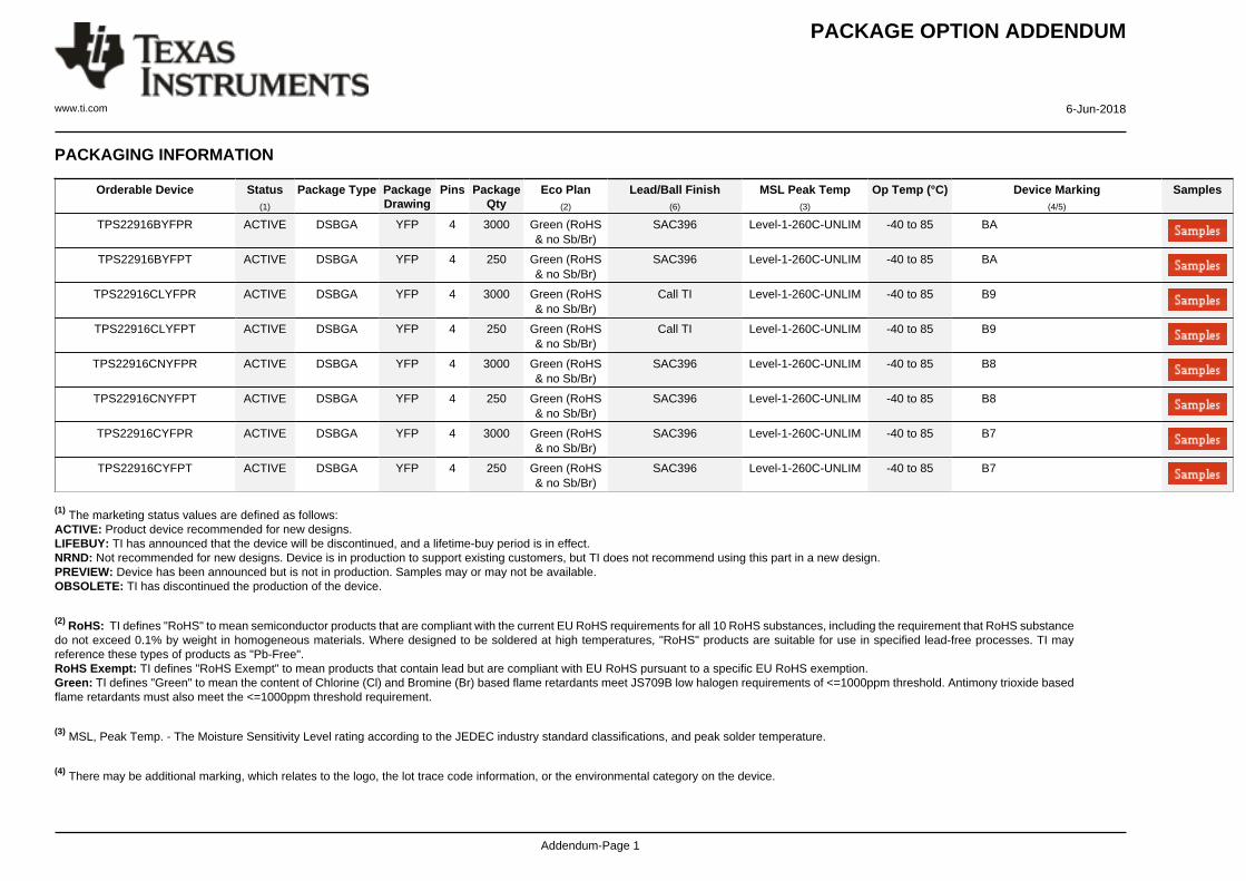
PACKAGING INFORMATION
Orderable Device Status(1)
Package Type PackageDrawing
Pins PackageQty
Eco Plan(2)
Lead/Ball Finish(6)
MSL Peak Temp(3)
Op Temp (°C) Device Marking(4/5)
Samples
TPS22916BYFPR ACTIVE DSBGA YFP 4 3000 Green (RoHS& no Sb/Br)
SAC396 Level-1-260C-UNLIM -40 to 85 BA
TPS22916BYFPT ACTIVE DSBGA YFP 4 250 Green (RoHS& no Sb/Br)
SAC396 Level-1-260C-UNLIM -40 to 85 BA
TPS22916CLYFPR ACTIVE DSBGA YFP 4 3000 Green (RoHS& no Sb/Br)
Call TI Level-1-260C-UNLIM -40 to 85 B9
TPS22916CLYFPT ACTIVE DSBGA YFP 4 250 Green (RoHS& no Sb/Br)
Call TI Level-1-260C-UNLIM -40 to 85 B9
TPS22916CNYFPR ACTIVE DSBGA YFP 4 3000 Green (RoHS& no Sb/Br)
SAC396 Level-1-260C-UNLIM -40 to 85 B8
TPS22916CNYFPT ACTIVE DSBGA YFP 4 250 Green (RoHS& no Sb/Br)
SAC396 Level-1-260C-UNLIM -40 to 85 B8
TPS22916CYFPR ACTIVE DSBGA YFP 4 3000 Green (RoHS& no Sb/Br)
SAC396 Level-1-260C-UNLIM -40 to 85 B7
TPS22916CYFPT ACTIVE DSBGA YFP 4 250 Green (RoHS& no Sb/Br)
SAC396 Level-1-260C-UNLIM -40 to 85 B7
(1) The marketing status values are defined as follows:ACTIVE: Product device recommended for new designs.LIFEBUY: TI has announced that the device will be discontinued, and a lifetime-buy period is in effect.NRND: Not recommended for new designs. Device is in production to support existing customers, but TI does not recommend using this part in a new design.PREVIEW: Device has been announced but is not in production. Samples may or may not be available.OBSOLETE: TI has discontinued the production of the device.
(2) RoHS: TI defines "RoHS" to mean semiconductor products that are compliant with the current EU RoHS requirements for all 10 RoHS substances, including the requirement that RoHS substancedo not exceed 0.1% by weight in homogeneous materials. Where designed to be soldered at high temperatures, "RoHS" products are suitable for use in specified lead-free processes. TI mayreference these types of products as "Pb-Free".RoHS Exempt: TI defines "RoHS Exempt" to mean products that contain lead but are compliant with EU RoHS pursuant to a specific EU RoHS exemption.Green: TI defines "Green" to mean the content of Chlorine (Cl) and Bromine (Br) based flame retardants meet JS709B low halogen requirements of <=1000ppm threshold. Antimony trioxide basedflame retardants must also meet the <=1000ppm threshold requirement.
(3) MSL, Peak Temp. - The Moisture Sensitivity Level rating according to the JEDEC industry standard classifications, and peak solder temperature.
(4) There may be additional marking, which relates to the logo, the lot trace code information, or the environmental category on the device.

PACKAGE OPTION ADDENDUM
www.ti.com 6-Jun-2018
Addendum-Page 2
(5) Multiple Device Markings will be inside parentheses. Only one Device Marking contained in parentheses and separated by a "~" will appear on a device. If a line is indented then it is a continuationof the previous line and the two combined represent the entire Device Marking for that device.
(6) Lead/Ball Finish - Orderable Devices may have multiple material finish options. Finish options are separated by a vertical ruled line. Lead/Ball Finish values may wrap to two lines if the finishvalue exceeds the maximum column width.
Important Information and Disclaimer:The information provided on this page represents TI's knowledge and belief as of the date that it is provided. TI bases its knowledge and belief on informationprovided by third parties, and makes no representation or warranty as to the accuracy of such information. Efforts are underway to better integrate information from third parties. TI has taken andcontinues to take reasonable steps to provide representative and accurate information but may not have conducted destructive testing or chemical analysis on incoming materials and chemicals.TI and TI suppliers consider certain information to be proprietary, and thus CAS numbers and other limited information may not be available for release.
In no event shall TI's liability arising out of such information exceed the total purchase price of the TI part(s) at issue in this document sold by TI to Customer on an annual basis.

TAPE AND REEL INFORMATION
*All dimensions are nominal
Device PackageType
PackageDrawing
Pins SPQ ReelDiameter
(mm)
ReelWidth
W1 (mm)
A0(mm)
B0(mm)
K0(mm)
P1(mm)
W(mm)
Pin1Quadrant
TPS22916BYFPR DSBGA YFP 4 3000 180.0 8.4 0.86 0.86 0.59 4.0 8.0 Q1
TPS22916BYFPT DSBGA YFP 4 250 180.0 8.4 0.86 0.86 0.59 4.0 8.0 Q1
TPS22916CLYFPR DSBGA YFP 4 3000 180.0 8.4 0.86 0.86 0.59 4.0 8.0 Q1
TPS22916CLYFPT DSBGA YFP 4 250 180.0 8.4 0.86 0.86 0.59 4.0 8.0 Q1
TPS22916CNYFPR DSBGA YFP 4 3000 180.0 8.4 0.86 0.86 0.59 4.0 8.0 Q1
TPS22916CNYFPT DSBGA YFP 4 250 180.0 8.4 0.86 0.86 0.59 4.0 8.0 Q1
TPS22916CYFPR DSBGA YFP 4 3000 180.0 8.4 0.86 0.86 0.59 4.0 8.0 Q1
TPS22916CYFPT DSBGA YFP 4 250 180.0 8.4 0.86 0.86 0.59 4.0 8.0 Q1
PACKAGE MATERIALS INFORMATION
www.ti.com 21-Dec-2017
Pack Materials-Page 1

*All dimensions are nominal
Device Package Type Package Drawing Pins SPQ Length (mm) Width (mm) Height (mm)
TPS22916BYFPR DSBGA YFP 4 3000 182.0 182.0 20.0
TPS22916BYFPT DSBGA YFP 4 250 182.0 182.0 20.0
TPS22916CLYFPR DSBGA YFP 4 3000 182.0 182.0 20.0
TPS22916CLYFPT DSBGA YFP 4 250 182.0 182.0 20.0
TPS22916CNYFPR DSBGA YFP 4 3000 182.0 182.0 20.0
TPS22916CNYFPT DSBGA YFP 4 250 182.0 182.0 20.0
TPS22916CYFPR DSBGA YFP 4 3000 182.0 182.0 20.0
TPS22916CYFPT DSBGA YFP 4 250 182.0 182.0 20.0
PACKAGE MATERIALS INFORMATION
www.ti.com 21-Dec-2017
Pack Materials-Page 2

www.ti.com
PACKAGE OUTLINE
C0.5 MAX
0.190.13
0.4TYP
0.4TYP
4X 0.250.21
B E A
D
4223507/A 01/2017
DSBGA - 0.5 mm max heightYFP0004DIE SIZE BALL GRID ARRAY
NOTES: 1. All linear dimensions are in millimeters. Any dimensions in parenthesis are for reference only. Dimensioning and tolerancing per ASME Y14.5M. 2. This drawing is subject to change without notice.
BALL A1CORNER
SEATING PLANE
BALL TYP 0.05 C
A
B
20.015 C A B
SYMM
SYMM
1
SCALE 10.000
D: Max =
E: Max =
0.77 mm, Min =
0.77 mm, Min =
0.71 mm
0.71 mm

www.ti.com
EXAMPLE BOARD LAYOUT
4X ( 0.23)
(0.4) TYP
(0.4) TYP
( 0.23)METAL
0.05 MAX
SOLDER MASKOPENING
METAL UNDERSOLDER MASK
( 0.23)SOLDER MASKOPENING
0.05 MIN
4223507/A 01/2017
DSBGA - 0.5 mm max heightYFP0004DIE SIZE BALL GRID ARRAY
NOTES: (continued) 3. Final dimensions may vary due to manufacturing tolerance considerations and also routing constraints. For more information, see Texas Instruments literature number SNVA009 (www.ti.com/lit/snva009).
SOLDER MASK DETAILSNOT TO SCALE
SYMM
SYMM
LAND PATTERN EXAMPLEEXPOSED METAL SHOWN
SCALE:50X
A
B
1 2
NON-SOLDER MASKDEFINED
(PREFERRED)
EXPOSEDMETAL
SOLDER MASKDEFINED
EXPOSEDMETAL

www.ti.com
EXAMPLE STENCIL DESIGN
(0.4) TYP
(0.4) TYP
4X ( 0.25) (R0.05) TYP
METALTYP
4223507/A 01/2017
DSBGA - 0.5 mm max heightYFP0004DIE SIZE BALL GRID ARRAY
NOTES: (continued) 4. Laser cutting apertures with trapezoidal walls and rounded corners may offer better paste release.
SYMM
SYMM
SOLDER PASTE EXAMPLEBASED ON 0.1 mm THICK STENCIL
SCALE:50X
A
B
1 2

IMPORTANT NOTICE
Texas Instruments Incorporated (TI) reserves the right to make corrections, enhancements, improvements and other changes to itssemiconductor products and services per JESD46, latest issue, and to discontinue any product or service per JESD48, latest issue. Buyersshould obtain the latest relevant information before placing orders and should verify that such information is current and complete.TI’s published terms of sale for semiconductor products (http://www.ti.com/sc/docs/stdterms.htm) apply to the sale of packaged integratedcircuit products that TI has qualified and released to market. Additional terms may apply to the use or sale of other types of TI products andservices.Reproduction of significant portions of TI information in TI data sheets is permissible only if reproduction is without alteration and isaccompanied by all associated warranties, conditions, limitations, and notices. TI is not responsible or liable for such reproduceddocumentation. Information of third parties may be subject to additional restrictions. Resale of TI products or services with statementsdifferent from or beyond the parameters stated by TI for that product or service voids all express and any implied warranties for theassociated TI product or service and is an unfair and deceptive business practice. TI is not responsible or liable for any such statements.Buyers and others who are developing systems that incorporate TI products (collectively, “Designers”) understand and agree that Designersremain responsible for using their independent analysis, evaluation and judgment in designing their applications and that Designers havefull and exclusive responsibility to assure the safety of Designers' applications and compliance of their applications (and of all TI productsused in or for Designers’ applications) with all applicable regulations, laws and other applicable requirements. Designer represents that, withrespect to their applications, Designer has all the necessary expertise to create and implement safeguards that (1) anticipate dangerousconsequences of failures, (2) monitor failures and their consequences, and (3) lessen the likelihood of failures that might cause harm andtake appropriate actions. Designer agrees that prior to using or distributing any applications that include TI products, Designer willthoroughly test such applications and the functionality of such TI products as used in such applications.TI’s provision of technical, application or other design advice, quality characterization, reliability data or other services or information,including, but not limited to, reference designs and materials relating to evaluation modules, (collectively, “TI Resources”) are intended toassist designers who are developing applications that incorporate TI products; by downloading, accessing or using TI Resources in anyway, Designer (individually or, if Designer is acting on behalf of a company, Designer’s company) agrees to use any particular TI Resourcesolely for this purpose and subject to the terms of this Notice.TI’s provision of TI Resources does not expand or otherwise alter TI’s applicable published warranties or warranty disclaimers for TIproducts, and no additional obligations or liabilities arise from TI providing such TI Resources. TI reserves the right to make corrections,enhancements, improvements and other changes to its TI Resources. TI has not conducted any testing other than that specificallydescribed in the published documentation for a particular TI Resource.Designer is authorized to use, copy and modify any individual TI Resource only in connection with the development of applications thatinclude the TI product(s) identified in such TI Resource. NO OTHER LICENSE, EXPRESS OR IMPLIED, BY ESTOPPEL OR OTHERWISETO ANY OTHER TI INTELLECTUAL PROPERTY RIGHT, AND NO LICENSE TO ANY TECHNOLOGY OR INTELLECTUAL PROPERTYRIGHT OF TI OR ANY THIRD PARTY IS GRANTED HEREIN, including but not limited to any patent right, copyright, mask work right, orother intellectual property right relating to any combination, machine, or process in which TI products or services are used. Informationregarding or referencing third-party products or services does not constitute a license to use such products or services, or a warranty orendorsement thereof. Use of TI Resources may require a license from a third party under the patents or other intellectual property of thethird party, or a license from TI under the patents or other intellectual property of TI.TI RESOURCES ARE PROVIDED “AS IS” AND WITH ALL FAULTS. TI DISCLAIMS ALL OTHER WARRANTIES ORREPRESENTATIONS, EXPRESS OR IMPLIED, REGARDING RESOURCES OR USE THEREOF, INCLUDING BUT NOT LIMITED TOACCURACY OR COMPLETENESS, TITLE, ANY EPIDEMIC FAILURE WARRANTY AND ANY IMPLIED WARRANTIES OFMERCHANTABILITY, FITNESS FOR A PARTICULAR PURPOSE, AND NON-INFRINGEMENT OF ANY THIRD PARTY INTELLECTUALPROPERTY RIGHTS. TI SHALL NOT BE LIABLE FOR AND SHALL NOT DEFEND OR INDEMNIFY DESIGNER AGAINST ANY CLAIM,INCLUDING BUT NOT LIMITED TO ANY INFRINGEMENT CLAIM THAT RELATES TO OR IS BASED ON ANY COMBINATION OFPRODUCTS EVEN IF DESCRIBED IN TI RESOURCES OR OTHERWISE. IN NO EVENT SHALL TI BE LIABLE FOR ANY ACTUAL,DIRECT, SPECIAL, COLLATERAL, INDIRECT, PUNITIVE, INCIDENTAL, CONSEQUENTIAL OR EXEMPLARY DAMAGES INCONNECTION WITH OR ARISING OUT OF TI RESOURCES OR USE THEREOF, AND REGARDLESS OF WHETHER TI HAS BEENADVISED OF THE POSSIBILITY OF SUCH DAMAGES.Unless TI has explicitly designated an individual product as meeting the requirements of a particular industry standard (e.g., ISO/TS 16949and ISO 26262), TI is not responsible for any failure to meet such industry standard requirements.Where TI specifically promotes products as facilitating functional safety or as compliant with industry functional safety standards, suchproducts are intended to help enable customers to design and create their own applications that meet applicable functional safety standardsand requirements. Using products in an application does not by itself establish any safety features in the application. Designers mustensure compliance with safety-related requirements and standards applicable to their applications. Designer may not use any TI products inlife-critical medical equipment unless authorized officers of the parties have executed a special contract specifically governing such use.Life-critical medical equipment is medical equipment where failure of such equipment would cause serious bodily injury or death (e.g., lifesupport, pacemakers, defibrillators, heart pumps, neurostimulators, and implantables). Such equipment includes, without limitation, allmedical devices identified by the U.S. Food and Drug Administration as Class III devices and equivalent classifications outside the U.S.TI may expressly designate certain products as completing a particular qualification (e.g., Q100, Military Grade, or Enhanced Product).Designers agree that it has the necessary expertise to select the product with the appropriate qualification designation for their applicationsand that proper product selection is at Designers’ own risk. Designers are solely responsible for compliance with all legal and regulatoryrequirements in connection with such selection.Designer will fully indemnify TI and its representatives against any damages, costs, losses, and/or liabilities arising out of Designer’s non-compliance with the terms and provisions of this Notice.
Mailing Address: Texas Instruments, Post Office Box 655303, Dallas, Texas 75265Copyright © 2018, Texas Instruments Incorporated