TPS75003 - Datasheet - Texas · PDF fileTPS75003 SBVS052I – OCTOBER 2004– REVISED...
32
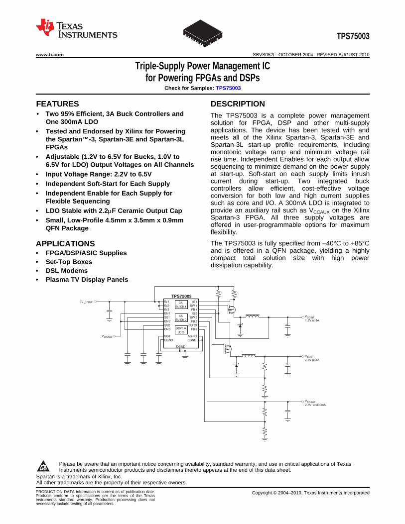
IN1 IN2 IN3 EN 1 SS1 EN 2 SS2 EN 3 IS1 SW 1 FB 1 IS2 SW 2 FB 2 OU T3 FB 3 DG ND 3A BU CK 1 3A BU CK 2 300m A LD O SS3 DGND AG ND DGND TPS75003 + + V CCAUX 2.5V at 300mA V CCO 3.3V at 3A V CCINT 1.2V at 3A V CCAUX 5V _Input TPS75003 www.ti.com SBVS052I – OCTOBER 2004 – REVISED AUGUST 2010 Triple-Supply Power Management IC for Powering FPGAs and DSPs Check for Samples: TPS75003 1FEATURES DESCRIPTION 23• Two 95% Efficient, 3A Buck Controllers and The TPS75003 is a complete power management One 300mA LDO solution for FPGA, DSP and other multi-supply applications. The device has been tested with and • Tested and Endorsed by Xilinx for Powering meets all of the Xilinx Spartan-3, Spartan-3E and the Spartan™-3, Spartan-3E and Spartan-3L Spartan-3L start-up profile requirements, including FPGAs monotonic voltage ramp and minimum voltage rail • Adjustable (1.2V to 6.5V for Bucks, 1.0V to rise time. Independent Enables for each output allow 6.5V for LDO) Output Voltages on All Channels sequencing to minimize demand on the power supply at start-up. Soft-start on each supply limits inrush • Input Voltage Range: 2.2V to 6.5V current during start-up. Two integrated buck • Independent Soft-Start for Each Supply controllers allow efficient, cost-effective voltage • Independent Enable for Each Supply for conversion for both low and high current supplies Flexible Sequencing such as core and I/O. A 300mA LDO is integrated to provide an auxiliary rail such as V CCAUX on the Xilinx • LDO Stable with 2.2mF Ceramic Output Cap Spartan-3 FPGA. All three supply voltages are • Small, Low-Profile 4.5mm x 3.5mm x 0.9mm offered in user-programmable options for maximum QFN Package flexibility. The TPS75003 is fully specified from –40°C to +85°C APPLICATIONS and is offered in a QFN package, yielding a highly • FPGA/DSP/ASIC Supplies compact total solution size with high power • Set-Top Boxes dissipation capability. • DSL Modems • Plasma TV Display Panels 1 Please be aware that an important notice concerning availability, standard warranty, and use in critical applications of Texas Instruments semiconductor products and disclaimers thereto appears at the end of this data sheet. 2Spartan is a trademark of Xilinx, Inc. 3All other trademarks are the property of their respective owners. PRODUCTION DATA information is current as of publication date. Copyright © 2004–2010, Texas Instruments Incorporated Products conform to specifications per the terms of the Texas Instruments standard warranty. Production processing does not necessarily include testing of all parameters.
Transcript of TPS75003 - Datasheet - Texas · PDF fileTPS75003 SBVS052I – OCTOBER 2004– REVISED...
IN1
IN2
IN3
EN 1
SS1
EN 2
SS2
EN 3
IS1
SW 1
FB 1
IS2
SW 2
FB 2
OUT3
FB 3
DGND
3A
BU CK 1
3A
BU CK 2
300m A
LD O
SS3
DGND
AG ND
DGND
TPS75003
+
+
VCCAUX
2.5V at 300mA
VCCO
3.3V at 3A
VCCINT
1.2V at 3A
VCCAUX
5V _Input
TPS75003
www.ti.com SBVS052I –OCTOBER 2004–REVISED AUGUST 2010
Triple-Supply Power Management ICfor Powering FPGAs and DSPs
Check for Samples: TPS75003
1FEATURES DESCRIPTION23• Two 95% Efficient, 3A Buck Controllers and The TPS75003 is a complete power management
One 300mA LDO solution for FPGA, DSP and other multi-supplyapplications. The device has been tested with and• Tested and Endorsed by Xilinx for Poweringmeets all of the Xilinx Spartan-3, Spartan-3E andthe Spartan™-3, Spartan-3E and Spartan-3LSpartan-3L start-up profile requirements, includingFPGAsmonotonic voltage ramp and minimum voltage rail
• Adjustable (1.2V to 6.5V for Bucks, 1.0V to rise time. Independent Enables for each output allow6.5V for LDO) Output Voltages on All Channels sequencing to minimize demand on the power supply
at start-up. Soft-start on each supply limits inrush• Input Voltage Range: 2.2V to 6.5Vcurrent during start-up. Two integrated buck• Independent Soft-Start for Each Supplycontrollers allow efficient, cost-effective voltage
• Independent Enable for Each Supply for conversion for both low and high current suppliesFlexible Sequencing such as core and I/O. A 300mA LDO is integrated to
provide an auxiliary rail such as VCCAUX on the Xilinx• LDO Stable with 2.2mF Ceramic Output CapSpartan-3 FPGA. All three supply voltages are• Small, Low-Profile 4.5mm x 3.5mm x 0.9mmoffered in user-programmable options for maximumQFN Packageflexibility.
The TPS75003 is fully specified from –40°C to +85°CAPPLICATIONSand is offered in a QFN package, yielding a highly• FPGA/DSP/ASIC Suppliescompact total solution size with high power
• Set-Top Boxes dissipation capability.• DSL Modems• Plasma TV Display Panels
1
Please be aware that an important notice concerning availability, standard warranty, and use in critical applications of TexasInstruments semiconductor products and disclaimers thereto appears at the end of this data sheet.
2Spartan is a trademark of Xilinx, Inc.3All other trademarks are the property of their respective owners.
PRODUCTION DATA information is current as of publication date. Copyright © 2004–2010, Texas Instruments IncorporatedProducts conform to specifications per the terms of the TexasInstruments standard warranty. Production processing does notnecessarily include testing of all parameters.

TPS75003
SBVS052I –OCTOBER 2004–REVISED AUGUST 2010 www.ti.com
This integrated circuit can be damaged by ESD. Texas Instruments recommends that all integrated circuits be handled withappropriate precautions. Failure to observe proper handling and installation procedures can cause damage.
ESD damage can range from subtle performance degradation to complete device failure. Precision integrated circuits may be moresusceptible to damage because very small parametric changes could cause the device not to meet its published specifications.
ORDERING INFORMATION (1)
PRODUCT VOUT
Buck1: AdjustableTPS75003 Buck2: Adjustable
LDO: Adjustable
(1) For the most current specifications and package information, see the Package Option Addendum located at the end of this document, orsee the TI website at www.ti.com.
ABSOLUTE MAXIMUM RATINGSOver operating free-air temperature range (unless otherwise noted) (1)
TPS75003 UNIT
VINX range (IN1, IN2, IN3) –0.3 to +7.0 V
VENX range (EN1, EN2, EN3) –0.3 to VINX +0.3 V
VSWX range (SW1, SW2, SW3) –0.3 to VINX +0.3 V
VISX range (IS1, IS2, IS3) –0.3 to VINX +0.3 V
VOUT3 range –0.3 to +7.0 V
VSSX range (SS1, SS2, SS3) –0.3 to VINX +0.3 V
VFBX range (FB1, FB2, FB3) –0.3 to +3.3 V
Peak LDO output current (IOUT3) Internally limited —
Continuous total power dissipation See Dissipation Ratings Table —
Junction temperature range, TJ –55 to +150 °C
Storage temperature range –65 to +150 °C
ESD rating, HBM 1 kV
ESD rating, CDM 500 V
(1) Stresses beyond those listed under absolute maximum ratings may cause permanent damage to the device. These are stress ratingsonly, and functional operation of the device at these or any other conditions beyond those indicated under the Electrical Characteristicsis not implied. Exposure to absolute maximum rated conditions for extended periods may affect device reliability.
THERMAL INFORMATIONTPS75003
THERMAL METRIC (1) (2) UNITSRHL (20 PINS)
qJA Junction-to-ambient thermal resistance 42.6
qJCtop Junction-to-case (top) thermal resistance 51.8
qJB Junction-to-board thermal resistance 39.5°C/W
yJT Junction-to-top characterization parameter 0.6
yJB Junction-to-board characterization parameter 14.2
qJCbot Junction-to-case (bottom) thermal resistance 2.8
(1) For more information about traditional and new thermal metrics, see the IC Package Thermal Metrics application report, SPRA953.(2) For thermal estimates of this device based on PCB copper area, see the TI PCB Thermal Calculator.
2 Submit Documentation Feedback Copyright © 2004–2010, Texas Instruments Incorporated
Product Folder Link(s): TPS75003

TPS75003
www.ti.com SBVS052I –OCTOBER 2004–REVISED AUGUST 2010
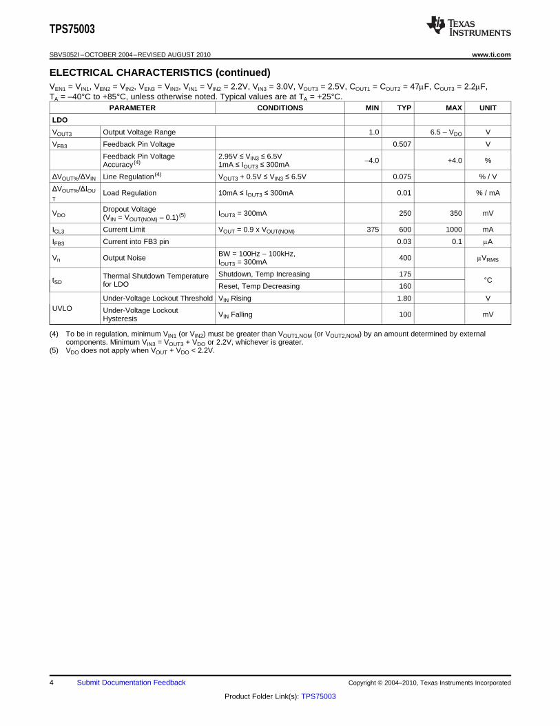
ELECTRICAL CHARACTERISTICSVEN1 = VIN1, VEN2 = VIN2, VEN3 = VIN3, VIN1 = VIN2 = 2.2V, VIN3 = 3.0V, VOUT3 = 2.5V, COUT1 = COUT2 = 47mF, COUT3 = 2.2mF,TA = –40°C to +85°C, unless otherwise noted. Typical values are at TA = +25°C.
PARAMETER CONDITIONS MIN TYP MAX UNIT
Supply and Logic
Input Voltage RangeVINX 2.2 6.5 V(IN1, IN2, IN3) (1)
Quiescent Current, IQ = IDGND +IQ IOUT1 = IOUT2 = 0mA, IOUT3 = 1mA 75 150 mAIAGND
ISHDN Shutdown Supply Current VEN1 = VEN2 = VEN3 = 0V 0.05 3.0 mA
Enable High, enabledVIH1, 2 1.4 VINX V(EN1, EN2)
VIH3 Enable High, enabled (EN3) 1.14 VIN3 V
Enable Low, shutdownVILX 0 0.3 V(EN1, EN2, EN3)
Enable pin currentIENX 0.01 0.5 mA(EN1, EN2, EN3)
Buck Controllers 1 and 2
Adjustable Output VoltageVOUT1,2 VFBX VINX VRange (2)
VFB1,2 Feedback Voltage (FB1, FB2) 1.220 V
Feedback Voltage Accuracy (1)–2 +2 %(FB1, FB2)
IFB1,2 Current into FB1, FB2 pins 0.01 0.5 mA
Reference Voltage for CurrentVIS1,2 80 100 120 mVSense
IIS1,2 Current into IS1, IS2 Pins 0.01 0.5 mA
Measured with the circuit in Figure 1,ΔVOUT%/ΔVIN Line Regulation (1) 0.1 % / VVOUT + 0.5V ≤ VIN ≤ 6.5V
ΔVOUT%/ΔIOU Measured with the circuit in Figure 1,Load Regulation 0.6 % / AT 30mA ≤ I OUT ≤ 2A
Measured with the circuit in Figure 1,n 1,2 Efficiency (3) 94 %IOUT = 1A
Measured with the circuit in Figure 1,tSTR1,2 Startup Time (3) 5 msRL = 6Ω, COUT = 100mF, CSS = 2.2nF
Gate Driver P-Channel and VIN1,2 > 2.5V 4RDS,ON1,2 N-Channel MOSFET Ω
VIN1,2 = 2.2V 6On-Resistance
Gate Driver P-Channel andISW1,2 N-Channel MOSFET Drive 100 mA
Current
tON Minimum On Time 1.36 1.55 1.84 ms
tOFF Minimum Off Time 0.44 0.65 0.86 ms
(1) To be in regulation, minimum VIN1 (or VIN2) must be greater than VOUT1,NOM (or VOUT2,NOM) by an amount determined by externalcomponents. Minimum VIN3 = VOUT3 + VDO or 2.2V, whichever is greater.
(2) Maximum VOUT depends on external components and will be less than VIN.(3) Depends on external components.
Copyright © 2004–2010, Texas Instruments Incorporated Submit Documentation Feedback 3
Product Folder Link(s): TPS75003
TPS75003
SBVS052I –OCTOBER 2004–REVISED AUGUST 2010 www.ti.com
ELECTRICAL CHARACTERISTICS (continued)VEN1 = VIN1, VEN2 = VIN2, VEN3 = VIN3, VIN1 = VIN2 = 2.2V, VIN3 = 3.0V, VOUT3 = 2.5V, COUT1 = COUT2 = 47mF, COUT3 = 2.2mF,TA = –40°C to +85°C, unless otherwise noted. Typical values are at TA = +25°C.
PARAMETER CONDITIONS MIN TYP MAX UNIT
LDO
VOUT3 Output Voltage Range 1.0 6.5 – VDO V
VFB3 Feedback Pin Voltage 0.507 V
Feedback Pin Voltage 2.95V ≤ VIN3 ≤ 6.5V –4.0 +4.0 %Accuracy (4) 1mA ≤ IOUT3 ≤ 300mA
ΔVOUT%/ΔVIN Line Regulation (4) VOUT3 + 0.5V ≤ VIN3 ≤ 6.5V 0.075 % / V
ΔVOUT%/ΔIOU Load Regulation 10mA ≤ IOUT3 ≤ 300mA 0.01 % / mAT
Dropout VoltageVDO IOUT3 = 300mA 250 350 mV(VIN = VOUT(NOM) – 0.1) (5)
ICL3 Current Limit VOUT = 0.9 x VOUT(NOM) 375 600 1000 mA
IFB3 Current into FB3 pin 0.03 0.1 mA
BW = 100Hz – 100kHz,Vn Output Noise 400 mVRMSIOUT3 = 300mA
Shutdown, Temp Increasing 175Thermal Shutdown TemperaturetSD °Cfor LDO Reset, Temp Decreasing 160
Under-Voltage Lockout Threshold VIN Rising 1.80 VUVLO Under-Voltage Lockout VIN Falling 100 mVHysteresis
(4) To be in regulation, minimum VIN1 (or VIN2) must be greater than VOUT1,NOM (or VOUT2,NOM) by an amount determined by externalcomponents. Minimum VIN3 = VOUT3 + VDO or 2.2V, whichever is greater.
(5) VDO does not apply when VOUT + VDO < 2.2V.
4 Submit Documentation Feedback Copyright © 2004–2010, Texas Instruments Incorporated
Product Folder Link(s): TPS75003
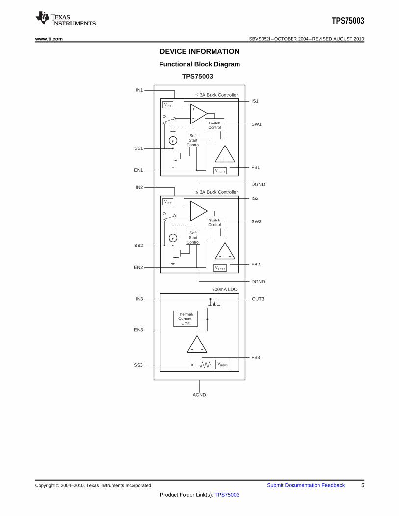
VREF1
SoftStart
Control
SwitchControl
VIS1
IS1
SW1
FB1EN1
SS1
IN1≤ 3A Buck Controller
DGND
VREF2
SoftStart
Control
SwitchControl
VIS2
IS2
SW2
FB2EN2
SS2
IN2≤ 3A Buck Controller
DGND
FB3
OUT3IN3
EN3
SS3
Thermal/Current
Limit
300mA LDO
VREF3
AGND
TPS75003
TPS75003
www.ti.com SBVS052I –OCTOBER 2004–REVISED AUGUST 2010
DEVICE INFORMATION
Functional Block Diagram
Copyright © 2004–2010, Texas Instruments Incorporated Submit Documentation Feedback 5
Product Folder Link(s): TPS75003

IN3
OUT3
FB1
FB2
20
1
11
10
DGND
SS
3
AG
ND
EN
1
SS
1
DG
ND
SW
1
IN1
IS1
19
18
17
16
15
14
13
12
FB
3
EN
3
EN
2
SS
2
DG
ND
SW
2
IN2
IS2
2 3 4 5 6 7 8 9
RHL PACKAGE4.5mm x 3.5mm QFN
(TOP VIEW)
TPS75003
SBVS052I –OCTOBER 2004–REVISED AUGUST 2010 www.ti.com
TERMINAL FUNCTIONSTERMINAL
DESCRIPTIONNAME RHL
Ground connection for BUCK1 and BUCK2 converters. Pins 6 and 15 should be connected to the backDGND 6, 15, PAD side exposed pad by a short metal trace as shown in the PCB Layout section of this data sheet.
AGND 18 Ground connection for LDO.
IN1 13 Input supply to BUCK1.
IN2 8 Input supply to BUCK2.
IN3 20 Input supply to LDO.
Driving the enable pin (ENx) high turns on BUCK1 regulator. Driving this pin low puts it into shutdownEN1 17 mode, reducing operating current. The enable pin does not trigger on fast negative going transients.
EN2 4 Same as EN1 but for BUCK2 controller.
EN3 3 Same as EN1 but for LDO.
Connecting a capacitor between this pin and ground increases start-up time of the BUCK1 regulator bySS1 16 slowing the ramp-up of current limit. This high-impedance pin is noise-sensitive; careful layout is
important. See the Typical Characteristics, Applications, and PCB Layout sections for details.
SS2 5 Same as SS1 but for BUCK2 regulator.
Connecting a capacitor from this pin to ground slows the start-up time of the LDO reference, therbySS3 19 slowing output voltage ramp-up. See the Applications section for details.
Current sense input for BUCK1 regulator. The voltage difference between this pin and IN1 is comparedIS1 12 to an internal reference to set current limit. For a robust output start-up ramp, careful layout and
bypassing are required. See the Applications section for details.
IS2 9 Same as IS1 but compared to IN2 and used for BUCK2 controller.
SW1 14 Gate drive pin for external BUCK1 P-channel MOSFET.
SW2 7 Same as SW1 but for BUCK2 controller.
FB1 11 Feedback pin. Used to set the output voltage of BUCK1 regulator.
FB2 10 Same as FB1 but for BUCK2 controller.
FB3 2 Same as FB1 but for LDO.
Regulated LDO output. A small ceramic capacitor (≥ 2.2mF) is needed from this pin to ground to ensureOUT3 1 stability.
6 Submit Documentation Feedback Copyright © 2004–2010, Texas Instruments Incorporated
Product Folder Link(s): TPS75003
L15µHSumidaCDRH6D38−5R0
IN3
OUT3
FB1
FB2
20
1
11
10
DGND
SS
3
AG
ND
EN
1
SS
1
DG
ND
SW
1
IN1
IS1
19 18 17 16 15 14 13 12
FB
3
EN
3
EN
2
SS
2
DG
ND
SW
2
IN2
IS2
2 3 4 5 6 7 8 9R361.9kΩ
R415.4kΩ
EN3EN2
VIN
EN1
VIN
1.5nF
1.5nF0.01µF R133mΩ
10pF
100µFTantalum
100µFTantalum
SiliconixSi2323DS
SiliconixSi2323DS
Q2
L215µHSumidaCDRH8D43−150
VCCINT1.2V, 2AVishay
SS32D2
0.1µF
1µF
VCCAUX2.5V, 300mA
10µF
0.1µF
R561.9kΩ
ON SemiconductorMBRM120
R636.5kΩ
VCCO3.3V, 2A
R233mΩ
100µFVIN
Q1
0 0.5 1.0 1.5 2.0 2.5 3.0 3.5
IOUT (A)
VIN = 3.3VVOUT = 1.2V
TA = +85C
TA = −40C
TA = +25C
5
4
3
2
1
0
−1
−2
−3
−4
−5
∆V
OU
T(%
)
0 0.5 1.0 1.5 2.0 2.5 3.0 3.5
IOUT (A)
VIN = 5VVOUT = 3.3V
5
4
3
2
1
0
−1
−2
−3
−4
−5
∆V
OU
T(%
) TA = +85C
TA = −40C
TA = +25C
TPS75003
www.ti.com SBVS052I –OCTOBER 2004–REVISED AUGUST 2010
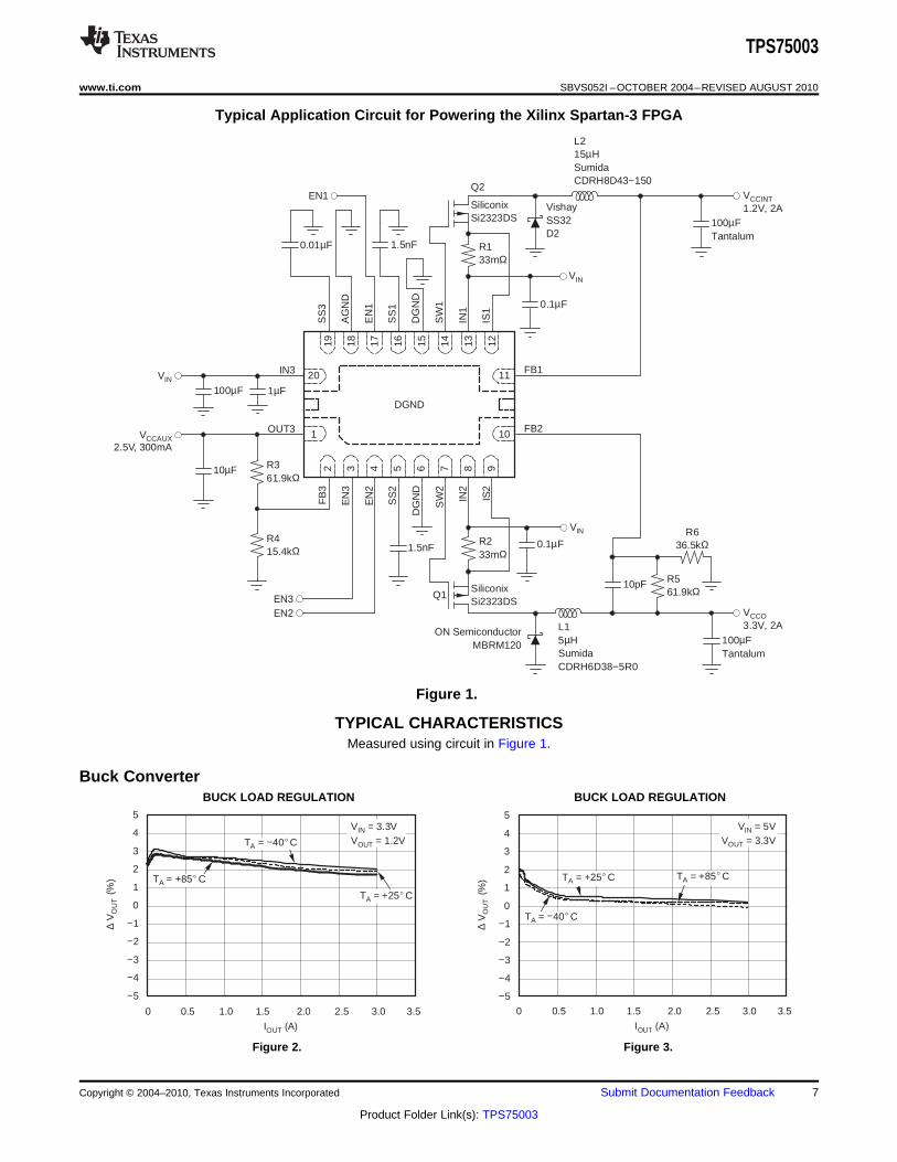
Typical Application Circuit for Powering the Xilinx Spartan-3 FPGA
Figure 1.
TYPICAL CHARACTERISTICSMeasured using circuit in Figure 1.
Buck ConverterBUCK LOAD REGULATION BUCK LOAD REGULATION
Figure 2. Figure 3.
Copyright © 2004–2010, Texas Instruments Incorporated Submit Documentation Feedback 7
Product Folder Link(s): TPS75003

3.0
VIN (V)
5
4
3
2
1
0
−1
−2
−3
−4
−5
∆V
OU
T( %
)
VOUT = 3.3VIOUT = 2A
3.5 4.0 4.5 5.0 5.5 6.0 6.5 7.0
TA = +85C
TA = +25C
TA = −40C
2.0
VIN (V)
5
4
3
2
1
0
−1
−2
−3
−4
−5
∆V
OU
T( %
)
VOUT = 1.2VIOUT = 2A
2.5 3.0 3.5 4.0 4.5 5.0 5.5 6.0 6.5 7.0
TA = −40CTA = +25C
TA = +85C
0 0.5 1.0 1.5 2.0 2.5 3.0
500
400
300
200
100
0
Sw
itchi
ng
Fre
que
ncy
(kH
z)
IOUT (A)
VOUT = 1.2V
VIN = 3.3V
VIN = 5.0V−40C+25C
+85C
600
500
400
300
200
100
0
Sw
itchi
ng
Fre
que
ncy
(kH
z)
0.01 0.1 1.0 10
IOUT (A)
VIN = 5.0VVOUT = 1.2V
VIN = 3.3V
VOUT = 1.2V
VIN = 5.0VVOUT = 3.3V
VOUT = 1.2VVIN = 2.2V
1µs/div
VIN = 5.0VVOUT = 3.3VIOUT = 2A
20m
V/d
iv
100
90
80
70
60
50
40
30
20
10
0
Eff
icie
ncy
(%)
0.0001 0.001 0.01 0.1 1 10
IOUT (A)
VIN = 5.0VVOUT = 3.3V
VIN = 3.3V
VOUT = 1.2V
VIN = 5.0VVOUT = 1.2V
TPS75003
SBVS052I –OCTOBER 2004–REVISED AUGUST 2010 www.ti.com
TYPICAL CHARACTERISTICS (continued)Measured using circuit in Figure 1.
BUCK LINE REGULATION BUCK LINE REGULATION
Figure 4. Figure 5.
BUCK SWITCHING FREQUENCY BUCK SWITCHING FREQUENCYvs vs
IOUT, TA IOUT
Figure 6. Figure 7.
EFFICIENCY vsBUCK OUTPUT VOLTAGE RIPPLE IOUT
Figure 8. Figure 9.
8 Submit Documentation Feedback Copyright © 2004–2010, Texas Instruments Incorporated
Product Folder Link(s): TPS75003

EN
VIN = 5V, COUT = 330µF
VIN = 5V, COUT = 100µF
VIN = 3.3V, COUT = 680µF
VIN = 3.3V, COUT = 100µF
CSS = 0.01µFVOUT = 1.2V
20ms/div
VO
UT
(500
mV
/div
)
ENVIN = 5V, IOUT = 0.5A
VIN = 5V, IOUT = 1.0A
VIN = 5V, IOUT = 2.0A
VIN = 3.3V, IOUT = 1.0A
CSS = 0.01µFVOUT = 1.2V
20ms/div
VO
UT
(50
0mV
/div
)
VIN = 3.3V, IOUT = 2.0A
ENVIN = 3.3V, CSS = 0.001µF
VIN = 5V, CSS = 0.001µF
VIN = 5V, CSS = 0.01µF
VIN = 3.3V, CSS = 0.01µF
IOUT = 1AVOUT = 1.2V
20ms/div
VO
UT
(500
mV
/div
)
EN
IOUT = 2A,CSS = 560pF
IOUT = 0.5A,CSS = 560pF
IOUT = 0.5A, CSS = 1500pF
IOUT = 2A, CSS = 1500pF
VIN = 5VVOUT = 3.3V
5ms/div
VO
UT
(2V
/div
)
EN VIN = 3.3V,IOUT = 1A,RS = 0.020
VIN =5V, IOUT = 1A,RS = 0.033
VIN = 3.3V,IOUT = 1A,RS = 0.033
VIN = 5V,IOUT = 1A,RS = 0.020
VOUT = 1.2V, CSS = 0.01µF
20ms/div
VO
UT
(1V
/div
)
TPS75003
www.ti.com SBVS052I –OCTOBER 2004–REVISED AUGUST 2010
TYPICAL CHARACTERISTICS (continued)Measured using circuit in Figure 1.
BUCK START-UP BUCK START-UPvs vs
VIN and IOUT(1) VIN and COUT
(1)
Figure 10. Figure 11.
BUCK START-UP BUCK START-UPvs vs
VIN and CSS(1) IOUT and CSS
(1)
Figure 12. Figure 13.
BUCK START-UPvs
VIN and RSENSE(1)
Figure 14.
(1)xxxSee the section, Soft-Start Capacitor Selection (Buck Controllers) .
(1) See the section, Soft-Start Capacitor Selection (Buck Controllers) .
Copyright © 2004–2010, Texas Instruments Incorporated Submit Documentation Feedback 9
Product Folder Link(s): TPS75003

∆VO
UT (
%)
0 0.05 0.1 0.15 0.2 0.25 0.3 0.35 0.4
5
4
3
2
1
0
−1
−2
−3
−4
−5
IOUT (A)
VIN = 3.3VVOUT = 2.5V
TA = +25C
TA = +85C
TA = −40C
∆VO
UT (
%)
3.0 3.5 4.0 4.5 5.0 5.5 6.0 6.5 7.0
VIN (V)
VOUT = 2.5VIOUT = 1mA
TA = +85C
5
4
3
2
1
0
−1
−2
−3
−4
−5
TA = +25C
TA = −40C
450
400
350
300
250
200
150
100
50
0
VD
O(m
V)
Ambient Temperature (C)
−40 −25 −10 5 20 35 50 65 8580
VOUT = 2.5VIOUT = 300mA
500
400
300
200
100
0
VD
O(m
V)
0 50 100 150 200 250 300 350 400 450
IOUT (mA)
TA = −40C
TA = +25C
TA = +85C
VIN = 3.3VVOUT = 2.5V
2.0 2.5 3.0 3.5 4.0 4.5 5.0 5.5 6.0 6.5 7.0
12
10
8
6
4
2
0
RD
S,O
N(
Ω)
VIN (V)
TA = −40C
TA = +25C
TA = +85C
2.0 2.5 3.0 3.5 4.0 4.5 5.0 5.5 6.0 6.5 7.0
12
10
8
6
4
2
0
RD
S,O
N(
Ω)
VIN (V)
TA = −40C
TA = +25C
TA = +85C
TPS75003
SBVS052I –OCTOBER 2004–REVISED AUGUST 2010 www.ti.com
TYPICAL CHARACTERISTICS (continued)Measured using circuit in Figure 1.
LDO ConverterLDO LOAD REGULATION LDO LINE REGULATION
Figure 15. Figure 16.
LDO DROPOUT LDO DROPOUTvs vs
IOUT TA
Figure 17. Figure 18.
RDS,ON PMOS vs VIN RDS,ON NMOS vs VIN
Figure 19. Figure 20.
10 Submit Documentation Feedback Copyright © 2004–2010, Texas Instruments Incorporated
Product Folder Link(s): TPS75003
2.525
2.520
2.515
2.510
2.505
2.500
2.495
2.490
2.485
2.480
2.475
VO
UT
(V)
−40 −15 10 35 60 85
Ambient Temperature (C)
VIN = 3.3V
TPS75003
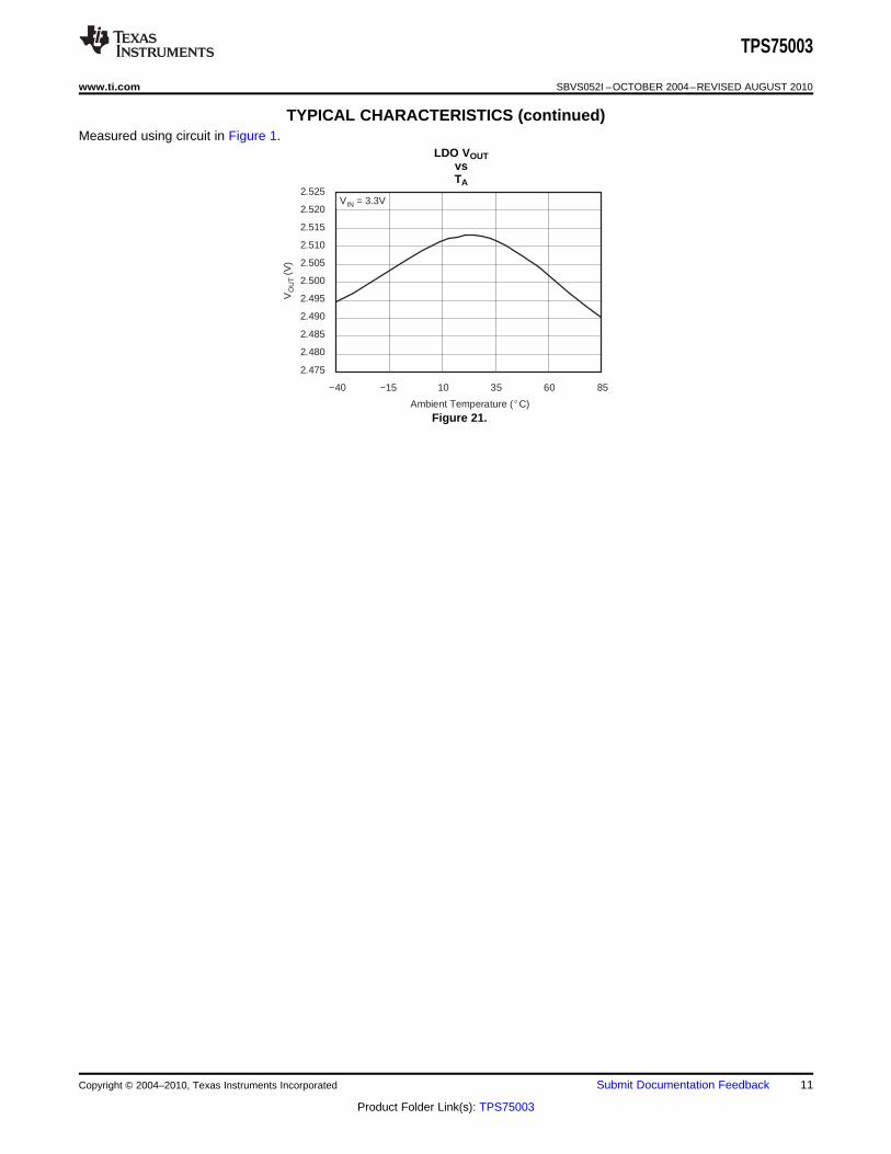
www.ti.com SBVS052I –OCTOBER 2004–REVISED AUGUST 2010
TYPICAL CHARACTERISTICS (continued)Measured using circuit in Figure 1.
LDO VOUTvsTA
Figure 21.
Copyright © 2004–2010, Texas Instruments Incorporated Submit Documentation Feedback 11
Product Folder Link(s): TPS75003

TPS75003
SBVS052I –OCTOBER 2004–REVISED AUGUST 2010 www.ti.com
APPLICATION INFORMATION
The TPS75003 is an integrated power management IC designed specifically to power DSPs and FPGAs such asthe Xilinx Spartan-3, Spartan-3E and Spartan-3L. Two non-synchronous buck controllers can be configured tosupply up to 3A for both CORE and I/O rails. A low dropout linear regulator powers auxiliary rails up to 300mA.All channels have independent enable and soft-start, allowing control of inrush current and output voltage ramptime as required by the application.
Figure 1 shows a typical application circuit for powering the Xilinx Spartan-3 FPGA. Table 1 through Table 4show component values that have been tested for use with up to 3A load currents. Inductors in Table 1 aretested up to the respective saturation currents. Other similar external components can be substituted as desired;however, in all cases the circuits that are used should be tested for compliance to application requirements.
Table 1. Inductors Tested with the TPS75003
PART NUMBER MANUFACTURER INDUCTANCE DC RESISTANCE SATURATION CURRENT
SLF7032T−100M1R4 TDK 10mH ±20% 53mΩ ±20% 1.4A
SLF6025−150MR88 TDK 15mH ±20% 85mΩ ±20% 0.88A
CDRH6D28−5R0 Sumida 5mH 23mΩ 2.4A
CDRH6D38-5R0 Sumida 5mH 18mΩ 2.9A
CDRH103R−100 Sumida 10mH 45mΩ 2.4A
CDRH4D28−100 Sumida 10mH 96mΩ 1.0A
CDRH8D43-150 Sumida 15mH 42mΩ 2.9A
CDRH5D18−6R2 Sumida 6.2mH 71mΩ 1.4A
DO3316P−472 Coilcraft 4.7mH 18mΩ 5.4A
DT3316P−153 Coilcraft 15mH 60mΩ 1.8A
DT3316P−223 Coilcraft 22mH 84mΩ 1.5A
744052006 Wurth 6.2mH 80mΩ 1.45A
74451115 Wurth 15mH 90mΩ 0.8A
Table 2. PMOS Transistors Tested with the TPS75003
PART NUMBER MANUFACTURER RDS,ON (TYP) VDS ID PACKAGE
Si5447DC Vishay Siliconix 0.11Ω at VGS = –2.5V –20V –3.5A at +25°C 1206
Si5475DC Vishay Siliconix 0.041Ω at VGS = –2.5V –12V –6.6A at +25°C 1206
Si2323DS Vishay Siliconix 0.052Ω at VGS = –2.5V –20V –4.1A at +25°C SOT23
Si2301ADS Vishay Siliconix 0.19Ω at VGS = –2.5V –20V –1.4A at +25°C SOT23
Si2323DS Vishay Siliconix 0.41Ω at VGS = –2.5V –20V –4.1A at +25°C SOT23
FDG326P Fairchild 0.17Ω at VGS = –2.5V –20V –1.5A SC70
Table 3. Diodes Tested with the TPS75003
PART NUMBER MANUFACTURER VR IF PACKAGE
MBRM120LT3 ON Semiconductor 20V 1.0A DO216AA
MBR0530T1 ON Semiconductor 30V 1.5A SOD123
ZHCS2000TA Zetex 40V 2.0A SOT23−6
B320 Diodes Inc. 20V 3.0A SMA
SS32 Fairchild 20V 3.0A DO214AB
12 Submit Documentation Feedback Copyright © 2004–2010, Texas Instruments Incorporated
Product Folder Link(s): TPS75003

0.1µF
R
D
Q L
f = measured resonantfrequency at switch node
R = 2πfL
TPS75003
www.ti.com SBVS052I –OCTOBER 2004–REVISED AUGUST 2010
Table 4. Capacitors Tested with the TPS75003
PART NUMBER MANUFACTURER CAPACITANCE ESR VOLTAGE RATING
6TPB47M (PosCap) Sanyo 47mF 0.1Ω 6.3V
T491D476M010AS Kemet 47mF 0.8Ω 10V
B45197A Epco 47mF 0.175Ω 16V
B45294−R1107−M40 Epco 100mF 0.045Ω 6.3V
594D476X0016C2 Vishay 47mF 0.11Ω 16V
594D127X96R3C2 Vishay 120mF 0.085Ω 6.3V
TPSC107K006R0150 AVX 100mF 0.15Ω 6.3V
6TPS100MC Sanyo 100mF 0.45Ω 6.3V
OPERATION (BUCK CONTROLLERS)
Channels 1 and 2 contain two identical non-synchronous buck controllers that use minimum on-time/minimumoff-time hysteretic control. (Refer to Figure 1.) For clarity, BUCK1 is used throughout the discussion of deviceoperation. When VOUT1 is below its target, an external PMOS (Q1) is turned on for at least the minimum on-time,increasing current through the inductor (L1) until VOUT1 reaches its target value or the current limit (set by R1) isreached. Once either of these conditions is met, the PMOS is switched off for at least the minimum off-time ofthe device. After the minimum off-time has passed, the output voltage is monitored and the switch is turned onagain when necessary.
When output current is low, the buck controllers operate in discontinuous mode. In this mode, each switchingcycle begins at zero inductor current, rises to a maximum value, then falls back to zero current. When currentreaches zero on the falling edge, ringing occurs at the resonant frequency of the inductor and stray switch nodecapacitance. This operation is normal; it does not affect circuit performance, and can be minimized if desired byusing an RC snubber and/or a resistor in series with the gate of the PMOS, as shown in Figure 22.
Figure 22. RC Snubber and Series Gate Resistor Used to Minimize Ringing
At higher output currents, the TPS75003 operates in continuous mode. In continuous mode, there is no ringing atthe switch node and VOUT is equal to VIN times the duty cycle of the switching waveform.
When VIN approaches or falls below VOUT, the buck controllers operate in 100% duty cycle mode, fully turning onthe external PMOS to allow regulation at lower dropout than would otherwise be possible.
Enable (Buck Controllers)
The enable pins (EN1 and EN2) for the buck controllers are active high. When the enable pin is driven low andinput voltage is present at IN1 or IN2, an on-chip FET is turned on to discharge the soft-start pin SS1 or SS2,respectively. If the soft-start feature is being used, enable should be driven high at least 10ms after VIN is appliedto ensure this discharge cycle occurs.
UVLO (Buck Controllers)
An under-voltage lockout circuit is present to prevent turning on the external PMOS (Q1 or Q2) until a reliableoperating voltage is reached on the appropriate regulator (IN1 or IN2). This prevents the buck controllers frommis-operation at low input voltages.
Copyright © 2004–2010, Texas Instruments Incorporated Submit Documentation Feedback 13
Product Folder Link(s): TPS75003

ILIMIT VIS1,2
R1,2
IRMS IOUT D IOUT
VOUT
V IN
PDISS IRMS2 R
TPS75003
SBVS052I –OCTOBER 2004–REVISED AUGUST 2010 www.ti.com
Current Limit (Buck Controllers)
An external resistor (R1 or R2) is used to set the current limit for the external PMOS transistor (Q1 or Q2). Theseresistors are connected between IN1 and IS1 (or IN2 and IS2) to provide a reference voltage across these pinsthat is proportional to the current flowing through the PMOS transistor. This reference voltage is compared to aninternal reference to determine if an over-current condition exists. When current limit is exceeded, the externalPMOS is turned off for the minimum off-time. Current limit detection is disabled for 10ns any time the PMOS isturned on to avoid triggering on switching noise. In 100% duty cycle mode, current limit is always enabled.Current limit is calculated using the VIS1 or VIS2 specification in the Electrical Characteristics section, shown inEquation 1:
(1)
The current limit resistor must be appropriately rated for the dissipated power determined by its RMS currentcalculated by Equation 2:
(2)
For low-cost applications the IS1,2 pin can be connected to the drain of the PMOS, using RDS,ON instead of R1 orR2 to set current limit. Variations in the PMOS RDS,ON must be taken into account to ensure that current limit willprotect external components such as the inductor, the diode, and the switch itself from damage as a result ofover-current.
Short-Circuit Protection (Buck Controllers)
In an overload condition, the current rating of the external components (PMOS, diode, and inductor) can beexceeded. To help guard against this, the TPS75003 increases its minimum off-time when the voltage at thefeedback pin is lower than the reference voltage. When the output is shorted (VFB is zero), minimum off-time isincreased to approximately 4ms. The increase in off-time is proportional to the difference between the voltage atthe feedback pin and the internal reference.
Soft-Start (Buck Controllers)
The buck controllers each have independent soft-start capability to limit inrush during start-up and to meet timingrequirements of the Xilinx Spartan-3 FPGA. Limiting inrush current by using soft-start, or by staggering theturn-on of power rails, also guards against voltage drops at the input source due to its output impedance. Referto the soft-start circuitry shown in Figure 23 and the soft-start timing diagram shown in Figure 24. BUCK 1 will bediscussed in this section; it is identical to BUCK2. Note that pins SS1 and SS2 are very high-impedance andcannot be probed using a typical oscilloscope setup. When input voltage is applied at IN1 and EN1 is driven low,any charge on the SS pin is discharged by an on-chip pull-down transistor. When EN1 is driven high, an on-chipcurrent source starts charging the external soft-start capacitor CSS1. The voltage on the capacitor is compared tothe voltage across the current sense resistor R1 to determine if an over-current condition exists. If the voltagedrop across the sense resistor goes above the reference voltage, then the external PMOS is shut off for theminimum off-time. This implementation provides a cycle-by-cycle current limit and allows the user to program thesoft-start time over a wide range for most applications. For detailed information on choosing CSS1 and CSS2, seethe section, Soft-Start Capacitor Selection (Buck Controllers) .
14 Submit Documentation Feedback Copyright © 2004–2010, Texas Instruments Incorporated
Product Folder Link(s): TPS75003

SoftStart
Control
SwitchControl
VIS1
EN1
SW1
IS1
IN1
SS1
VIN
CurrentLimit
VSS1
VEN1
Time
CIN, MIN
(12)L (IL)2
V(RIPPLE) V IN
(12)L 0.3 IOUT
2
V(RIPPLE) V IN
TPS75003
www.ti.com SBVS052I –OCTOBER 2004–REVISED AUGUST 2010
Figure 23. Soft-Start Circuitry
Figure 24. Soft-Start Timing Diagram
Input Capacitor CIN1, CIN2 Selection (Buck Controllers)
It is good analog design practice to place input capacitors near the inputs of the device in order to ensure a lowimpedance input supply. 10mF to 22mF of capacitance for each buck converter is adequate for most applications,and should be placed within 100mils (0.01in, or 2.54mm) of the IN1 and IN2 pins to minimize the effects ofpulsed current switching noise on the soft-start circuitry during the first ~1V of output voltage ramp. Low ESRcapacitors also help to minimize noise on the supply line. The minimum value of capacitance can be estimatedusing Equation 3:
(3)
Copyright © 2004–2010, Texas Instruments Incorporated Submit Documentation Feedback 15
Product Folder Link(s): TPS75003

IC,IN(RMS) IOUT VOUT
V IN, MIN
V INVOUTIOUT rDS(on)RL IOUT t(OFF,min)
VOUTVSCHOTTKYRL IOUT
tON, MIN
LMIN
VINVOUTIOUT rDS(on)RL IOUT tON, MIN
IL
LMIN
VOUTVSCHOTTKYRL IOUT tOFF, MIN
IL
IPMOS(RMS) IOUT D IOUT
VOUT
V IN
P(cond) IOUT D
2
rDS(on) 1TC TJ25C IOUT D rDS(on)
TPS75003
SBVS052I –OCTOBER 2004–REVISED AUGUST 2010 www.ti.com
Note that the capacitors must be able to handle the RMS current in continuous conduction mode, which can becalculated using Equation 4:
(4)
Inductor Value Selection (Buck Controllers)
The inductor is chosen based on inductance value and maximum current rating. Larger inductors reduce currentripple (and therefore, output voltage ripple) but are physically larger and more expensive. Inductors with lowerDC resistance typically improve efficiency, but also have higher cost and larger physical size. The buckconverters work well with inductor values between 4.7mH and 47mH in most applications. When selecting aninductor, the current rating should exceed the current limit set by RIS or RDS,ON (see the Current Limit section). Todetermine the minimum inductor size, first determine if the device will operate in minimum on-time or minimumoff-time mode. The device will operate in minimum on-time mode if Equation 5 is satisfied:
(5)
where RL = the inductor DC resistance.
Minimum inductor size needed when operating in minimum on-time mode is given by Equation 6:
(6)
Minimum inductor size needed when operating in minimum off-time mode is given by Equation 7:
(7)
where ΔIL = (20%–30%) x IOUT-MAX
External PMOS Transistor Selection (Buck Controllers)
The external PMOS transistor is selected based on threshold voltage (VT), on-resistance (RDS,ON), gatecapacitance (CG) and voltage rating. The PMOS VT magnitude must be much lower than the lowest voltage atIN1 or IN2 that will be used. A VT magnitude that is 0.5V less than the lowest input voltage is normally sufficient.The PMOS gate will see voltages from 0V to the maximum input voltage, so gate-to-source breakdown should bea few volts higher than the maximum input supply. The drain-to-source of the device will also see this full voltageswing, and should therefore be a few volts higher than the maximum input supply. The RMS current in the PMOScan be estimated by using Equation 8:
(8)
The power dissipated in the PMOS is comprised of both conduction and switching losses. Switching losses aretypically insignificant. The conduction losses are a function of the RMS current and the RDS,ON of the PMOS, andare calculated by Equation 9:
(9)
16 Submit Documentation Feedback Copyright © 2004–2010, Texas Instruments Incorporated
Product Folder Link(s): TPS75003

I(diode)(RMS) IOUT1D IOUT1VOUT
V IN
VPP I ESR 18 COUT f
1.1I ESR
COUT L IOUT
2
VINVOUT V
TPS75003
www.ti.com SBVS052I –OCTOBER 2004–REVISED AUGUST 2010
Diode Selection (Buck Controllers)
The diode is off when the PMOS is on, and on when the PMOS is off. Since it will be turned on and off at arelatively high frequency, a Schottky diode is recommended for good performance. The peak current rating of thediode should exceed the peak current limit set by the sense resistor RIS1,2. A diode with low reverse leakagecurrent and low forward voltage at operating current will optimize efficiency. Equation 10 calculates the estimatedaverage power dissipation:
(10)
Output Capacitor Selection (Buck Controllers)
The output capacitor is selected based on output voltage ripple and transient response requirements. As a resultof the nature of the hysteretic control loop, a minimum ESR of a few tens of mΩ should be maintained for goodoperation unless a feed-forward resistor is used. Low ESR bulk tantalum or PosCap capacitors work best in mostapplications. A 1.0mF ceramic capacitor can be used in parallel with this capacitor to filter higher frequencyspikes. The output voltage ripple can be estimated by Equation 11:
(11)
To calculate the capacitance needed to achieve a given voltage ripple as a result of a load transient from zerooutput to full current, use Equation 12:
(12)
If only ceramic or other very low ESR output capacitor configurations are desired, additional voltage ripple mustbe passed to the feedback pin. See Application Note SLVA210, Using Ceramic Output Capacitors with theTPS6420x and TPS75003 Buck Controllers, available for download at www.ti.com, for detailed applicationinformation.
Output Voltage Ripple Effect on VOUT (Buck Controllers)
Output voltage ripple causes VOUT to be higher or lower than the target value by half of the peak-to-peak voltageripple. For minimum on-time, the ripple adds to the voltage; for minimum off-time, it subtracts from the voltage.
Soft-Start Capacitor Selection (Buck Controllers)
The soft-start for BUCK1 and BUCK2 is not intended to be a precision function. However, the startup time (froma positive transition on Enable to VOUT reaching its final value) has a linear relationship to CSS up toapproximately 800pF, which results in a startup time of approximately 4ms. Above this value of CSS, the variationin start-up time increases rapidly. This variation can occur from unit to unit and even between the two BUCKcontrollers in one device. Therefore, do not depend on the soft-start feature for sequencing multiple supplies ifvalues of CSS greater than 800pF are used.
BUCK1 is discussed in this section; it is identical to BUCK2. Soft-start is implemented on the buck controllers byramping current limit from 0 to its target value (set by R1) over a user-defined time. This time is set by theexternal soft-start cap connected to pin SS1. If SS1 is left open, a small on-chip capacitor will provide a currentlimit ramp time of approximately 250ms. Figure 25 shows the effects of R1 and SS1 on the current limit start-upramp.
Copyright © 2004–2010, Texas Instruments Incorporated Submit Documentation Feedback 17
Product Folder Link(s): TPS75003
3.0A
CurrentLimit
0.7A
Time
R1 = 33mΩ
R1 = 143mΩ
CSS1 = 0.022µF
CSS1 = 0.022µF
CSS1 = 0.01µF
CSS1 = 0.01µF
VOUT VFBR5
R61
TPS75003
SBVS052I –OCTOBER 2004–REVISED AUGUST 2010 www.ti.com
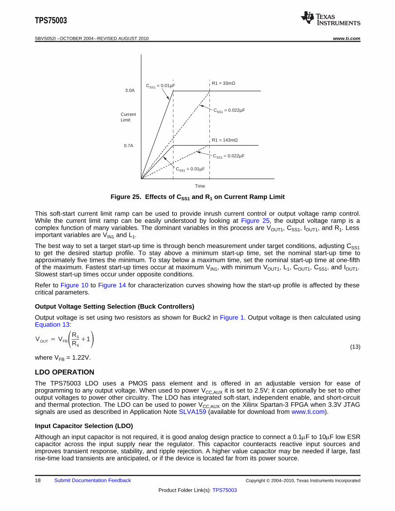
Figure 25. Effects of CSS1 and R1 on Current Ramp Limit
This soft-start current limit ramp can be used to provide inrush current control or output voltage ramp control.While the current limit ramp can be easily understood by looking at Figure 25, the output voltage ramp is acomplex function of many variables. The dominant variables in this process are VOUT1, CSS1, IOUT1, and R1. Lessimportant variables are VIN1 and L1.
The best way to set a target start-up time is through bench measurement under target conditions, adjusting CSS1to get the desired startup profile. To stay above a minimum start-up time, set the nominal start-up time toapproximately five times the minimum. To stay below a maximum time, set the nominal start-up time at one-fifthof the maximum. Fastest start-up times occur at maximum VIN1, with minimum VOUT1, L1, COUT1, CSS1, and IOUT1.Slowest start-up times occur under opposite conditions.
Refer to Figure 10 to Figure 14 for characterization curves showing how the start-up profile is affected by thesecritical parameters.
Output Voltage Setting Selection (Buck Controllers)
Output voltage is set using two resistors as shown for Buck2 in Figure 1. Output voltage is then calculated usingEquation 13:
(13)
where VFB = 1.22V.
LDO OPERATION
The TPS75003 LDO uses a PMOS pass element and is offered in an adjustable version for ease ofprogramming to any output voltage. When used to power VCC,AUX it is set to 2.5V; it can optionally be set to otheroutput voltages to power other circuitry. The LDO has integrated soft-start, independent enable, and short-circuitand thermal protection. The LDO can be used to power VCC,AUX on the Xilinx Spartan-3 FPGA when 3.3V JTAGsignals are used as described in Application Note SLVA159 (available for download from www.ti.com).
Input Capacitor Selection (LDO)
Although an input capacitor is not required, it is good analog design practice to connect a 0.1mF to 10mF low ESRcapacitor across the input supply near the regulator. This capacitor counteracts reactive input sources andimproves transient response, stability, and ripple rejection. A higher value capacitor may be needed if large, fastrise-time load transients are anticipated, or if the device is located far from its power source.
18 Submit Documentation Feedback Copyright © 2004–2010, Texas Instruments Incorporated
Product Folder Link(s): TPS75003

VOUT t VOUT,SET1 e
tRC
T90% 2.3 480x103 CSS3F
VOUT VFBR3
R41
TPS75003
www.ti.com SBVS052I –OCTOBER 2004–REVISED AUGUST 2010
Output Capacitor Selection (LDO)
A 2.2mF or greater capacitor is required near the output of the device to ensure stability. The LDO is stable withany capacitor type, including ceramic. If improved transient response or ripple rejection is required, larger and/orlower ESR output capacitors can be used.
Soft-Start (LDO)
The LDO uses an external soft-start capacitor, CSS3, to provide an RC-ramped reference voltage to the controlloop. (See the Functional Block Diagram.) This is a voltage-controlled soft-start, as compared to thecurrent-controlled soft-start used by the buck controllers. The start-up waveform can be approximated byEquation 14:
(14)
where R = 480 × 103 and C = capacitance in mF from SS3 to GND. The time taken to reach 90% of final VOUTcan be approximated by Equation 15:
(15)
Setting Output Voltage (LDO)
Output voltage is set using two resistors as shown in Figure 1. Output voltage is then calculated usingEquation 16:
(16)
where VFB = 0.507V.
Internal Current Limit (LDO)
The internal current limit of the LDO helps protect the regulator during fault conditions. When an over-currentcondition is detected, the output voltage will be reduced until the current falls to a level that will not damage thedevice. For good device reliability, the LDO should not operate at current limit.
Enable Pin (LDO)
The active high enable pin (EN3) can be used to put the device into shutdown mode. If shutdown and soft-startcapability are not required, EN3 can be tied to IN3.
Dropout Voltage (LDO)
The LDO uses a PMOS transistor to achieve low dropout. When (VIN – VOUT) is less than the dropout voltage(VDO), the pass device is in its linear region of operation, and the input-output resistance is the RDS,ON of the passtransistor. In this region, the regulator is said to be out of regulation; ripple rejection, line regulation, and loadregulation degrade as (VIN – VOUT) falls much below 0.5V.
Transient Response (LDO)
The LDO does not have an on-chip pull-down circuit for output is over-voltage conditions. This feature permitsapplications that connect higher voltage sources such as an alternate power supply to the output. This designalso results in an output overshoot of several percent if the load current quickly drops to zero. The amplitude ofovershoot can be reduced by increasing COUT; the duration of overshoot can be reduced by adding a loadresistor.
Thermal Protection (LDO)
Thermal protection disables the output when the junction temperature, TJ, reaches unsafe levels. When thejunction cools, the output is again enabled. Depending on power dissipation, thermal resistance, and ambienttemperature, the thermal protection circuit may cycle on and off. This cycling limits the dissipation of theregulator, protecting it from damage. For good long term reliability, the device should not be continuouslyoperated at or near thermal shutdown.
Copyright © 2004–2010, Texas Instruments Incorporated Submit Documentation Feedback 19
Product Folder Link(s): TPS75003

PD VIN3VOUT3 IOUT3
L1
IN3
OUT3
FB1
FB2
20
1
11
10
DGND
SS
3
AG
ND
EN
1
SS
1
DG
ND
SW
1
IN1
IS1
19
18
17
16
15
14
13
12
FB
3
EN
3
EN
2
SS
2
DG
ND
SW
2
IN2
IS2
2 3 4 5 6 7 8 9R6
R7
EN3EN2
VIN
EN1
VIN
C5,C18
C3,C17
C7R5
C10
C12, C16
C13, C15
Q1
Q2
L2VOUT1
D2
C9
C6
VOUT3
C14
C8
R9
D1
R8
VOUT2
R4
C1
VIN
TPS75003
SBVS052I –OCTOBER 2004–REVISED AUGUST 2010 www.ti.com
Power Dissipation (LDO)
The TPS75003 comes in a QFN-style package with an exposed lead frame on the package underside. Theexposed lead frame is the primary path for removing heat and should be soldered to a PC board that isconfigured to remove the amount of power dissipated by the LDO, as calculated by Equation 17:
(17)
Power dissipation can be minimized by using the lowest possible input voltage necessary to assure the requiredoutput voltage. The two buck converters do not contribute a significant amount of dissipated power. Usingheavier copper will increase the overall effectiveness of removing heat from the device. The addition of platedthrough-holes to heat-dissipating layers will also improve the heatsink effectiveness.
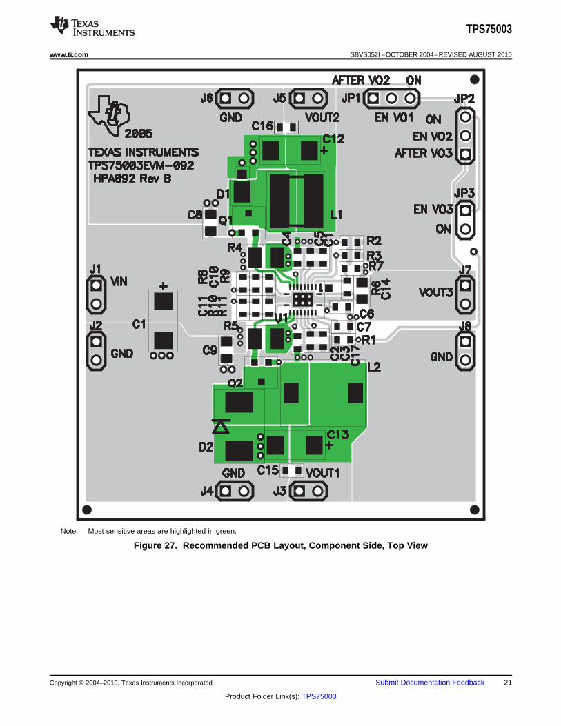
PCB Layout Considerations
As with any switching regulators, careful attention must be paid to board layout. A typical application circuit andcorresponding recommended printed circuit board (PCB) layout with emphasis on the most sensitive areas areshown in Figure 26 through Figure 28.
Note: Most sensitive areas are highlighted by bold lines.
Figure 26. Typical Application Circuit
20 Submit Documentation Feedback Copyright © 2004–2010, Texas Instruments Incorporated
Product Folder Link(s): TPS75003
TPS75003
www.ti.com SBVS052I –OCTOBER 2004–REVISED AUGUST 2010
Note: Most sensitive areas are highlighted in green.
Figure 27. Recommended PCB Layout, Component Side, Top View
Copyright © 2004–2010, Texas Instruments Incorporated Submit Documentation Feedback 21
Product Folder Link(s): TPS75003

TPS75003
SBVS052I –OCTOBER 2004–REVISED AUGUST 2010 www.ti.com
Note: Most sensitive areas are highlighted in green.
Figure 28. Recommended PCB Layout, Bottom Side, Top View
22 Submit Documentation Feedback Copyright © 2004–2010, Texas Instruments Incorporated
Product Folder Link(s): TPS75003
TPS75003
www.ti.com SBVS052I –OCTOBER 2004–REVISED AUGUST 2010
REVISION HISTORY
NOTE: Page numbers for previous revisions may differ from page numbers in the current version.
Changes from Revision H (August, 2008) to Revision I Page
• Replaced the Dissipation Ratings table with the Thermal Information table ........................................................................ 2
Copyright © 2004–2010, Texas Instruments Incorporated Submit Documentation Feedback 23
Product Folder Link(s): TPS75003

PACKAGE OPTION ADDENDUM
www.ti.com 27-Jul-2013
Addendum-Page 1
PACKAGING INFORMATION
Orderable Device Status(1)
Package Type PackageDrawing
Pins PackageQty
Eco Plan(2)
Lead/Ball Finish MSL Peak Temp(3)
Op Temp (°C) Device Marking(4/5)
Samples
TPS75003RHLR ACTIVE VQFN RHL 20 3000 Green (RoHS& no Sb/Br)
CU NIPDAU Level-1-260C-UNLIM -40 to 85 75003
TPS75003RHLRG4 ACTIVE VQFN RHL 20 3000 Green (RoHS& no Sb/Br)
CU NIPDAU Level-1-260C-UNLIM -40 to 85 75003
TPS75003RHLT ACTIVE VQFN RHL 20 250 Green (RoHS& no Sb/Br)
CU NIPDAU Level-1-260C-UNLIM -40 to 85 75003
TPS75003RHLTG4 ACTIVE VQFN RHL 20 250 Green (RoHS& no Sb/Br)
CU NIPDAU Level-1-260C-UNLIM -40 to 85 75003
(1) The marketing status values are defined as follows:ACTIVE: Product device recommended for new designs.LIFEBUY: TI has announced that the device will be discontinued, and a lifetime-buy period is in effect.NRND: Not recommended for new designs. Device is in production to support existing customers, but TI does not recommend using this part in a new design.PREVIEW: Device has been announced but is not in production. Samples may or may not be available.OBSOLETE: TI has discontinued the production of the device.
(2) Eco Plan - The planned eco-friendly classification: Pb-Free (RoHS), Pb-Free (RoHS Exempt), or Green (RoHS & no Sb/Br) - please check http://www.ti.com/productcontent for the latest availabilityinformation and additional product content details.TBD: The Pb-Free/Green conversion plan has not been defined.Pb-Free (RoHS): TI's terms "Lead-Free" or "Pb-Free" mean semiconductor products that are compatible with the current RoHS requirements for all 6 substances, including the requirement thatlead not exceed 0.1% by weight in homogeneous materials. Where designed to be soldered at high temperatures, TI Pb-Free products are suitable for use in specified lead-free processes.Pb-Free (RoHS Exempt): This component has a RoHS exemption for either 1) lead-based flip-chip solder bumps used between the die and package, or 2) lead-based die adhesive used betweenthe die and leadframe. The component is otherwise considered Pb-Free (RoHS compatible) as defined above.Green (RoHS & no Sb/Br): TI defines "Green" to mean Pb-Free (RoHS compatible), and free of Bromine (Br) and Antimony (Sb) based flame retardants (Br or Sb do not exceed 0.1% by weightin homogeneous material)
(3) MSL, Peak Temp. -- The Moisture Sensitivity Level rating according to the JEDEC industry standard classifications, and peak solder temperature.
(4) There may be additional marking, which relates to the logo, the lot trace code information, or the environmental category on the device.
(5) Multiple Device Markings will be inside parentheses. Only one Device Marking contained in parentheses and separated by a "~" will appear on a device. If a line is indented then it is a continuationof the previous line and the two combined represent the entire Device Marking for that device.
Important Information and Disclaimer:The information provided on this page represents TI's knowledge and belief as of the date that it is provided. TI bases its knowledge and belief on informationprovided by third parties, and makes no representation or warranty as to the accuracy of such information. Efforts are underway to better integrate information from third parties. TI has taken and

PACKAGE OPTION ADDENDUM
www.ti.com 27-Jul-2013
Addendum-Page 2
continues to take reasonable steps to provide representative and accurate information but may not have conducted destructive testing or chemical analysis on incoming materials and chemicals.TI and TI suppliers consider certain information to be proprietary, and thus CAS numbers and other limited information may not be available for release.
In no event shall TI's liability arising out of such information exceed the total purchase price of the TI part(s) at issue in this document sold by TI to Customer on an annual basis.
OTHER QUALIFIED VERSIONS OF TPS75003 :
• Enhanced Product: TPS75003-EP
NOTE: Qualified Version Definitions:
• Enhanced Product - Supports Defense, Aerospace and Medical Applications

TAPE AND REEL INFORMATION
*All dimensions are nominal
Device PackageType
PackageDrawing
Pins SPQ ReelDiameter
(mm)
ReelWidth
W1 (mm)
A0(mm)
B0(mm)
K0(mm)
P1(mm)
W(mm)
Pin1Quadrant
TPS75003RHLR VQFN RHL 20 3000 330.0 12.4 3.8 4.8 1.6 8.0 12.0 Q1
TPS75003RHLT VQFN RHL 20 250 180.0 12.4 3.8 4.8 1.6 8.0 12.0 Q1
PACKAGE MATERIALS INFORMATION
www.ti.com 27-Jul-2013
Pack Materials-Page 1
*All dimensions are nominal
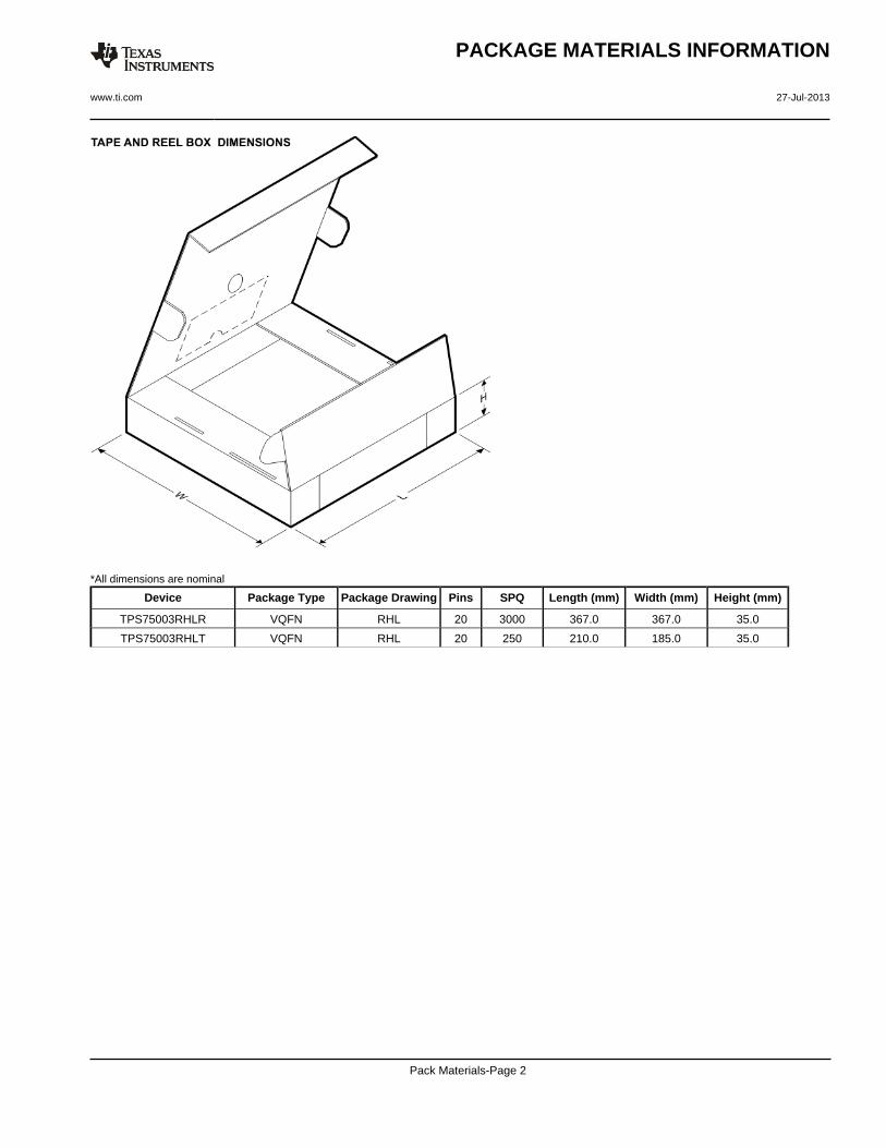
Device Package Type Package Drawing Pins SPQ Length (mm) Width (mm) Height (mm)
TPS75003RHLR VQFN RHL 20 3000 367.0 367.0 35.0
TPS75003RHLT VQFN RHL 20 250 210.0 185.0 35.0
PACKAGE MATERIALS INFORMATION
www.ti.com 27-Jul-2013
Pack Materials-Page 2

NOTES:
1. All linear dimensions are in millimeters. Any dimensions in parenthesis are for reference only. Dimensioning and tolerancingper ASME Y14.5M.
2. This drawing is subject to change without notice.3. The package thermal pad must be soldered to the printed circuit board for thermal and mechanical performance.
PACKAGE OUTLINE
4219071 / A 05/2017
www.ti.com
VQFN - 1 mm max height
PLASTIC QUAD FLATPACK- NO LEAD
RHL0020A
A
0.08 C
0.1 C A B0.05 C
B
SYMM
SYMM
PIN 1 INDEX AREA
SEATING PLANE
C
1PIN 1 ID(OPTIONAL)
2.05±0.1
3.05±0.1
3.63.4
4.64.4
1 MAX
(0.2) TYP
2X (0.55)
2X3.5
14X 0.5
2
9
10 11
12
19
20
2X 1.5
4X (0.2)
20X 0.290.19
20X 0.50.3
21
AutoCAD SHX Text
AutoCAD SHX Text

NOTES: (continued)
4. This package is designed to be soldered to a thermal pad on the board. For more information, see Texas Instrumentsliterature number SLUA271 (www.ti.com/lit/slua271) .
5. Solder mask tolerances between and around signal pads can vary based on board fabrication site.6. Vias are optional depending on application, refer to device data sheet. If any vias are implemented, refer to theri
locations shown on this view. It is recommended that vias under paste be filled, plugged or tented.
EXAMPLE BOARD LAYOUT
4219071 / A 05/2017
www.ti.com
VQFN - 1 mm max height
RHL0020A
PLASTIC QUAD FLATPACK- NO LEAD
SYMM
SYMM
LAND PATTERN EXAMPLEEXPOSED METAL SHOWN
SCALE: 18X
2X (1.5)
6X (0.525)
4X(0.775)
(4.3)
(3.3)
20X (0.6)
20X (0.24)
14X (0.5)
(3.05)
(2.05)
(R0.05) TYP
(Ø0.2) VIATYP)
1
2
9
10 11
12
19
20
0.07 MAXALL AROUND 0.07 MIN
ALL AROUND
SOLDER MASK DETAILS
NON SOLDER MASKDEFINED
(PREFERRED)
SOLDER MASKDEFINED
METAL
SOLDER MASKOPENING
SOLDER MASKOPENING
METAL UNDERSOLDER MASK
21
2X (0.75)
2X (0.4)
SOLDER MASKOPENING
METAL UNDERSOLDER MASK
4X (0.2)
2X (0.55)
EXPOSED METAL EXPOSED METAL
AutoCAD SHX Text
AutoCAD SHX Text

NOTES: (continued)
7. Laser cutting apertures with trapezoidal walls and rounded corners may offer better paste release. IPC-7525 may have alternatedesign recommendations..
EXAMPLE STENCIL DESIGN
4219071 / A 05/2017
www.ti.com
VQFN - 1 mm max height
RHL0020A
PLASTIC QUAD FLATPACK- NO LEAD
SYMM
SYMM
SOLDER PASTE EXAMPLEBASED ON 0.1mm THICK STENCIL
EXPOSED PAD75% PRINTED COVERAGE BY AREA
SCALE: 20X
(4.3)
2X (1.5)
(3.3)
(1.05)TYP
6X (0.92)
6X(0.85)
14X (0.5)
20X (0.24)
20X (0.6)
(0.56)TYP
METALTYP
21
4X (0.2)
2X (0.25)
(0.55)TYP
SOLDER MASK EDGETYP
2X(0.775)
1
2
9
10 11
12
19
20
(R0.05) TYP
AutoCAD SHX Text
AutoCAD SHX Text
IMPORTANT NOTICE
Texas Instruments Incorporated (TI) reserves the right to make corrections, enhancements, improvements and other changes to itssemiconductor products and services per JESD46, latest issue, and to discontinue any product or service per JESD48, latest issue. Buyersshould obtain the latest relevant information before placing orders and should verify that such information is current and complete.TI’s published terms of sale for semiconductor products (http://www.ti.com/sc/docs/stdterms.htm) apply to the sale of packaged integratedcircuit products that TI has qualified and released to market. Additional terms may apply to the use or sale of other types of TI products andservices.Reproduction of significant portions of TI information in TI data sheets is permissible only if reproduction is without alteration and isaccompanied by all associated warranties, conditions, limitations, and notices. TI is not responsible or liable for such reproduceddocumentation. Information of third parties may be subject to additional restrictions. Resale of TI products or services with statementsdifferent from or beyond the parameters stated by TI for that product or service voids all express and any implied warranties for theassociated TI product or service and is an unfair and deceptive business practice. TI is not responsible or liable for any such statements.Buyers and others who are developing systems that incorporate TI products (collectively, “Designers”) understand and agree that Designersremain responsible for using their independent analysis, evaluation and judgment in designing their applications and that Designers havefull and exclusive responsibility to assure the safety of Designers' applications and compliance of their applications (and of all TI productsused in or for Designers’ applications) with all applicable regulations, laws and other applicable requirements. Designer represents that, withrespect to their applications, Designer has all the necessary expertise to create and implement safeguards that (1) anticipate dangerousconsequences of failures, (2) monitor failures and their consequences, and (3) lessen the likelihood of failures that might cause harm andtake appropriate actions. Designer agrees that prior to using or distributing any applications that include TI products, Designer willthoroughly test such applications and the functionality of such TI products as used in such applications.TI’s provision of technical, application or other design advice, quality characterization, reliability data or other services or information,including, but not limited to, reference designs and materials relating to evaluation modules, (collectively, “TI Resources”) are intended toassist designers who are developing applications that incorporate TI products; by downloading, accessing or using TI Resources in anyway, Designer (individually or, if Designer is acting on behalf of a company, Designer’s company) agrees to use any particular TI Resourcesolely for this purpose and subject to the terms of this Notice.TI’s provision of TI Resources does not expand or otherwise alter TI’s applicable published warranties or warranty disclaimers for TIproducts, and no additional obligations or liabilities arise from TI providing such TI Resources. TI reserves the right to make corrections,enhancements, improvements and other changes to its TI Resources. TI has not conducted any testing other than that specificallydescribed in the published documentation for a particular TI Resource.Designer is authorized to use, copy and modify any individual TI Resource only in connection with the development of applications thatinclude the TI product(s) identified in such TI Resource. NO OTHER LICENSE, EXPRESS OR IMPLIED, BY ESTOPPEL OR OTHERWISETO ANY OTHER TI INTELLECTUAL PROPERTY RIGHT, AND NO LICENSE TO ANY TECHNOLOGY OR INTELLECTUAL PROPERTYRIGHT OF TI OR ANY THIRD PARTY IS GRANTED HEREIN, including but not limited to any patent right, copyright, mask work right, orother intellectual property right relating to any combination, machine, or process in which TI products or services are used. Informationregarding or referencing third-party products or services does not constitute a license to use such products or services, or a warranty orendorsement thereof. Use of TI Resources may require a license from a third party under the patents or other intellectual property of thethird party, or a license from TI under the patents or other intellectual property of TI.TI RESOURCES ARE PROVIDED “AS IS” AND WITH ALL FAULTS. TI DISCLAIMS ALL OTHER WARRANTIES ORREPRESENTATIONS, EXPRESS OR IMPLIED, REGARDING RESOURCES OR USE THEREOF, INCLUDING BUT NOT LIMITED TOACCURACY OR COMPLETENESS, TITLE, ANY EPIDEMIC FAILURE WARRANTY AND ANY IMPLIED WARRANTIES OFMERCHANTABILITY, FITNESS FOR A PARTICULAR PURPOSE, AND NON-INFRINGEMENT OF ANY THIRD PARTY INTELLECTUALPROPERTY RIGHTS. TI SHALL NOT BE LIABLE FOR AND SHALL NOT DEFEND OR INDEMNIFY DESIGNER AGAINST ANY CLAIM,INCLUDING BUT NOT LIMITED TO ANY INFRINGEMENT CLAIM THAT RELATES TO OR IS BASED ON ANY COMBINATION OFPRODUCTS EVEN IF DESCRIBED IN TI RESOURCES OR OTHERWISE. IN NO EVENT SHALL TI BE LIABLE FOR ANY ACTUAL,DIRECT, SPECIAL, COLLATERAL, INDIRECT, PUNITIVE, INCIDENTAL, CONSEQUENTIAL OR EXEMPLARY DAMAGES INCONNECTION WITH OR ARISING OUT OF TI RESOURCES OR USE THEREOF, AND REGARDLESS OF WHETHER TI HAS BEENADVISED OF THE POSSIBILITY OF SUCH DAMAGES.Unless TI has explicitly designated an individual product as meeting the requirements of a particular industry standard (e.g., ISO/TS 16949and ISO 26262), TI is not responsible for any failure to meet such industry standard requirements.Where TI specifically promotes products as facilitating functional safety or as compliant with industry functional safety standards, suchproducts are intended to help enable customers to design and create their own applications that meet applicable functional safety standardsand requirements. Using products in an application does not by itself establish any safety features in the application. Designers mustensure compliance with safety-related requirements and standards applicable to their applications. Designer may not use any TI products inlife-critical medical equipment unless authorized officers of the parties have executed a special contract specifically governing such use.Life-critical medical equipment is medical equipment where failure of such equipment would cause serious bodily injury or death (e.g., lifesupport, pacemakers, defibrillators, heart pumps, neurostimulators, and implantables). Such equipment includes, without limitation, allmedical devices identified by the U.S. Food and Drug Administration as Class III devices and equivalent classifications outside the U.S.TI may expressly designate certain products as completing a particular qualification (e.g., Q100, Military Grade, or Enhanced Product).Designers agree that it has the necessary expertise to select the product with the appropriate qualification designation for their applicationsand that proper product selection is at Designers’ own risk. Designers are solely responsible for compliance with all legal and regulatoryrequirements in connection with such selection.Designer will fully indemnify TI and its representatives against any damages, costs, losses, and/or liabilities arising out of Designer’s non-compliance with the terms and provisions of this Notice.
Mailing Address: Texas Instruments, Post Office Box 655303, Dallas, Texas 75265Copyright © 2018, Texas Instruments Incorporated