FMC-310€¦ · FMC-310 This electronics assembly can be damaged by ESD. Innovative Integration...
19
FMC-310 DESCRIPTION The FMC-310 is a high speed digitizing FMC module featuring four 310 MSPS A/D channels supported by sample clock and triggering features. Analog inputs may be either AC or DC coupled. Receiver IF frequencies of up to 300 MHz are supported in the standard model. The sample clock is from either an ultra-low-jitter PLL or external inputs. Multiple cards can be synchronized for sampling. Typical FMC-310 power consumption is 8.8W for typical AC coupled operation (10.8W typ. DC). The module may be conduction cooled using provided interfaces, which, while electrically isolated from circuit ground consistent with the FMC standard, connect the printed circuit board to thermal interfaces on both sides of the FMC-310 providing better and more thermal interfaces. Also the shielded circuits' shield (top removed in the above image) are thermally connected to the enclosed circuits, grounded, and can be used for heat management. Ruggedization levels for wide-temperature operation from -40 to +85C operation and 0.1 g 2 /Hz vibration. Conformal coating is available. Support logic in VHDL is provided for integration with FPGA carrier cards. Specific support for Innovative carrier cards includes integration with Framework Logic tools that support VHDL/Verilog and Matlab developers. The Matlab BSP supports real-time hardware-in- the-loop development using the graphical block diagram Simulink environment with Xilinx System Generator for the FMC integrated with the FPGA carrier card. Software tools for Innovative carrier cards include host development include C++ libraries and drivers for Windows and Linux. Application examples demonstrating the module features are provided. FEATURES • Four A/D Inputs • 310 MSPS, 16-bit • AC or DC coupled • Sample clocks and timing and controls • Both Front panel and FMC Ref Clock and Trig/Sync inputs • Front panel Clock/Vref output • Programmable PLL • 20 MHz TCXO Ref • FMC module, VITA 57.1 • High Pin Count • No SERDES required • 2.5V VADJ • Power monitor and controls • 8.8W typical (AC-coupled inputs) • Conduction Cooling Supported • Environmental ratings for -40 to 85C 9g RMS sine, 0.1g2/Hz random vibration APPLICATIONS • Wireless Receiver • LTE, WiMAX Physical Layer • RADAR • Medical Imaging • High Speed Data Recording SOFTWARE • MATLAB/VHDL FrameWork Logic Please be aware that an important notice concerning availability, standard warranty, and use in critical applications of Innovative Integration products and disclaimers thereto appears at the end of this data sheet. All trademarks are the property of their respective owners. PRODUCTION DATA information is current as of publication date. Products conform to specifications per the terms of the Innovative Integration standard warranty. Production processing does not necessarily include testing of all parameters. ©2014 Innovative Integration • phone 805.578.4260 • fax 805.578.4225 • www.innovative-dsp.com 05/20/16 FMC Module with 4x 310 MSPS 16-bit A/D with PLL and Timing Controls V1.14 2/8/15
Transcript of FMC-310€¦ · FMC-310 This electronics assembly can be damaged by ESD. Innovative Integration...

FMC-310
DESCRIPTIONThe FMC-310 is a high speed digitizing FMC module featuring four310 MSPS A/D channels supported by sample clock and triggeringfeatures. Analog inputs may be either AC or DC coupled. Receiver IFfrequencies of up to 300 MHz are supported in the standard model.The sample clock is from either an ultra-low-jitter PLL or externalinputs. Multiple cards can be synchronized for sampling.
Typical FMC-310 power consumption is 8.8W for typical AC coupledoperation (10.8W typ. DC). The module may be conduction cooledusing provided interfaces, which, while electrically isolated from circuitground consistent with the FMC standard, connect the printed circuitboard to thermal interfaces on both sides of the FMC-310 providingbetter and more thermal interfaces. Also the shielded circuits' shield(top removed in the above image) are thermally connected to theenclosed circuits, grounded, and can be used for heat management.Ruggedization levels for wide-temperature operation from -40 to +85Coperation and 0.1 g2/Hz vibration. Conformal coating is available.
Support logic in VHDL is provided for integration with FPGA carriercards. Specific support for Innovative carrier cards includesintegration with Framework Logic tools that support VHDL/Verilog andMatlab developers. The Matlab BSP supports real-time hardware-in-the-loop development using the graphical block diagram Simulinkenvironment with Xilinx System Generator for the FMC integrated withthe FPGA carrier card.
Software tools for Innovative carrier cards include host developmentinclude C++ libraries and drivers for Windows and Linux. Applicationexamples demonstrating the module features are provided.
FEATURES• Four A/D Inputs
• 310 MSPS, 16-bit• AC or DC coupled
• Sample clocks and timing and controls• Both Front panel and FMC Ref
Clock and Trig/Sync inputs• Front panel Clock/Vref output• Programmable PLL• 20 MHz TCXO Ref
• FMC module, VITA 57.1• High Pin Count
• No SERDES required• 2.5V VADJ
• Power monitor and controls• 8.8W typical (AC-coupled inputs)• Conduction Cooling Supported• Environmental ratings for -40 to 85C
9g RMS sine, 0.1g2/Hz random vibration
APPLICATIONS• Wireless Receiver• LTE, WiMAX Physical Layer• RADAR• Medical Imaging• High Speed Data Recording
SOFTWARE• MATLAB/VHDL FrameWork Logic
Please be aware that an important notice concerning availability, standard warranty, and use in critical applications of Innovative Integration products and disclaimers thereto appears at the end of this data sheet. All trademarks are the property of their respective owners.
PRODUCTION DATA information is current as of publication date. Products conform to specifications per the terms of the Innovative Integration standard warranty. Production processing does not necessarilyinclude testing of all parameters.
©2014 Innovative Integration • phone 805.578.4260 • fax 805.578.4225 • www.innovative-dsp.com05/20/16
FMC Module with 4x 310 MSPS 16-bit A/D with PLL and Timing Controls
V1.14 2/8/15
FMC-310This electronics assembly can be damaged by ESD. Innovative Integration recommends that all electronic assemblies and components circuits be handled with appropriate precautions. Failure to observe proper handling and installation procedures can cause damage. ESD damage can range from subtle performance degradation to complete device failure. Precision integrated circuits may be more susceptible to damage because very small parametric changes could cause the device not to meet its published specifications.
ORDERING INFORMATIONProduct Part No. Description
FMC-310 80320-1-<ER> FMC module with four 310 MSPS 16-bit A/Ds, PLL and timing controls, AC- coupled ADCs
FMC-310 80320-2-<ER> Like 80320-1 except ADCs are DC-coupled
Cables
SSMC to BNC cable 67156 IO cable with SSMC (male) to BNC (male), 1 meter
Carrier Cards
PEX6-COP 80284 Desktop/server PCI Express FPGA co-processor card with FMC site
SBC-K7 90326 Single board computer with Kintex 7 FPGA, COM Express
Embedded Computer Hosts
ePC-K7 90502 ePC-K7, I7 CPU, K325T2 Commercial FPGA. Embedded PC with support for two FMC modules; COM Express Type 6 CPU; Windows/Linux drivers
Mini-K7 90600 Mini-K7, I7 CPU, K325T2 Commercial FPGA. Embedded PC with support for one FMC modules; COM Express Type 6 CPU; Windows/Linux drivers
Physicals
Form Factor FMC VITA 57.1 single-width
Size 94.2 mm [front of assembly (RF connectors) to back of assembly (printed circuit board)] x 69 mm
10 mm mounting height
Weight 180g (approximate with conformal coat, contact factory if critical to application).
Hazardous Materials Lead-free and RoHS compliant
Innovative Integration • phone 805.578.4260 • fax 805.578.4225 • www.innovative-dsp.com 2 of 19
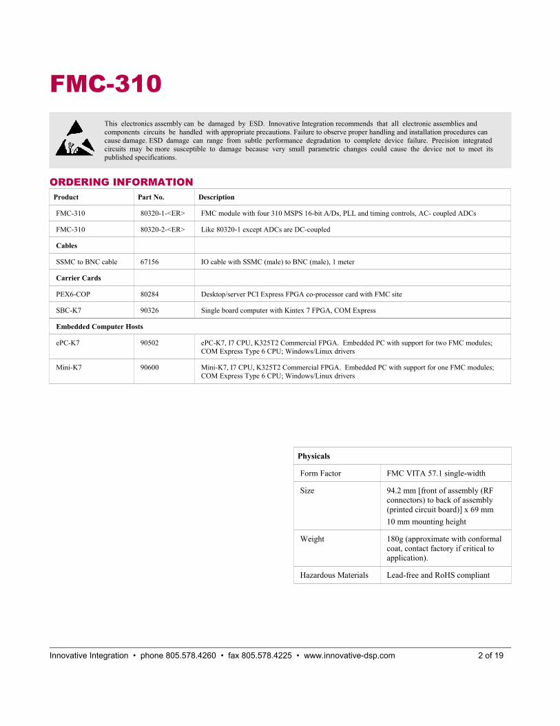
FMC-310
Front Panel (Bezel) Detail
Front PanelLabel
Schematicreference
Description
A/D 1 J1 A/D Analog Input 50 Ohm Nominal AC or DC coupled by model
A/D 0 J2 A/D Analog Input 50 Ohm Nominal AC or DC coupled by model
TRIG J5 DC coupled Logic Input 1.2 +/-0.1 V nominal threshold, 0 to 3.3V, High impedance
Clock In J6 AC coupled Logic Input 0.3 to 3.3Vpp AC (single to differential transformer to2 dB attenuator to PLL (LMK04828) clock input ) 1 to 750 MHz
Clock Out J7 Hardware Configurable IO, Standard configuration; sampling clock monitor 0.4V to 1.65 Vpp into 50 Ohms, with weak DC bias from Vref (1.25V nominal)
A/D 3 J3 A/D Analog Input 50 Ohm Nominal AC or DC coupled by model
A/D 2 J4 A/D Analog Input 50 Ohm Nominal AC or DC coupled by model
ALL ALL ENTERTEC 13460334 SSMC JACK RIGHT ANGLE EXTENDED BARREL
Innovative Integration • phone 805.578.4260 • fax 805.578.4225 • www.innovative-dsp.com 3 of 19

FMC-310Block Diagram Optional Feature Notes:
Optional Vos Servo Circuit:
The standard DC coupled FMC-310 employs digital calibration to remove input offset (Vos) which is the best choice for most applications. The superior analog performance of the DC coupled FMC-310 results from the use of a high performance differential input balanced amplifier. One amplifier input is used and the other is internally terminated to ground with a 50 Ohm resistor. But if there is a DC (or very low frequency) input applied to the FMC-310 input, the differential amplifier will see a DC bias or imbalance, typically reducing analog performance. The optional Vos servo converts an applied DC or low frequency input to differential at the amplifier inputs restoring the DC balance and bias point. This is also useful for reducing the FMC-310 hardware input offset, and accommodating non-50 Ohm inputs.
A trade off when using the optional FMC-310 Vos servo is it changes the DC coupled FMC-310 input impedance from approximately 50 Ohms at 200 Hz down to approximately 15 Ohms at DC, causes smaller (up to +/-8%) variation in the 50 Ohm input impedance between 200Hz and 120kHz, but is well matched to 50 Ohms above 120 kHz to the upper operating frequency limit. The servoed DC coupled FMC-310 will accurately measure a 50 Ohm series terminated input voltage down to DC, but the connected circuit will “see” the FMC-310 input impedance change at low frequencies.
Optional Voltage Reference Multiplexor/Distribution and J7 Clock/Vref Connector:
The standard configuration buffers the voltage reference from the A/D IC used for channels 1 and 2 to provide a DC levelat J7, allowing this to be used as a test point to verify the A/D's Vref setting. The optionally hardware configured Vref distribution circuit allows for either A/Ds' voltage reference, or an external Voltage reference applied to J7, to be scaled and source the other A/D's reference voltage or buffered to source J7's DC Voltage. Allowance is also made for using an internal low noise 1.8V supply as a reference. J7's circuit is configured as a bias tee allowing an AC coupled PLL output (could be sample clock, reference, sync or other PLL generated frequency) to be combined with this DC level.
Optional Attenuators or Low Pass Filters on FMC-310 Inputs:
On standard product these are populated with 1200 MHz (-1dB BW) low pass filters intended to filter high frequency EMI while not impacting signal bandwidth. Lower frequency options are possible. Attenuators can also be subsituted for filters with minimal EMC impact in most applications to attenuate the input, increasing input signal range and improving return loss. These also can be used in conjunction with...
Optional Filter, Peak and Match circuits at A/D IC Inputs:
A low pass filter and a bandpass filter are allowed for at the A/D IC input. These are designed to incorporate the A/D parasitic circuit in the filters, and reduce the broadband noise bandwidth at the A/D IC input.
Minimum lot sizes, set-up, stocking and NRE charges may apply. Contact sales support for pricing and availability.
Innovative Integration • phone 805.578.4260 • fax 805.578.4225 • www.innovative-dsp.com 4 of 19

FMC-310Operating Environment RatingsModules rated for operating environment temperature, shock and vibration are offered. The modules are qualified for wide temperature, vibration and shock to suit a variety of applications in each of the environmental ratings L0 through L4 and 100% tested for compliance. System compliance can depend on application, and system.
Environment Rating <ER>
L0 L1 L2 L3 L4
Environment Office, controlled lab
Outdoor, stationary Industrial Vehicles Military and heavy industry
Applications Lab instruments, research
Outdoor monitoring and controls
Industrial applications with moderate vibration
Manned vehicles Unmanned vehicles, missiles, oil and gas exploration
Cooling Forced Air
2 CFM
Forced Air
2 CFM
Conduction Conduction Conduction
Operating Temperature 0 to +50C -40 to +85C -20 to +65C -40 to +70C -40 to +85C
Storage Temperature -20 to +90C -40 to +100C -40 to +100C -40 to +100C -50 to +100C
Vibration Sine - - 2g
20-500 Hz
5g
20-2000 Hz
10g
20-2000 Hz
Random - - 0.04 g2/Hz
20-2000 Hz
0.1 g2/Hz
20-2000 Hz
0.1 g2/Hz
20-2000 Hz
Shock - - 20g, 11 ms 30g, 11 ms 40g, 11 ms
Humidity 0 to 95%,
non-condensing
0 to 100% 0 to 100% 0 to 100% 0 to 100%
Conformal coating Conformal coating Conformal coating,
extended temperature range devices
Conformal coating,
extended temperature range devices,
Thermal conduction assembly
Conformal coating,
extended temperature range devices,
Thermal conduction assembly,
Epoxy bonding for devices
Testing Functional,
Temperature cycling
Functional,
Temperature cycling,
Wide temperature testing
Functional,
Temperature cycling,
Wide temperature testing
Vibration, Shock
Functional,
Temperature cycling,
Wide temperature testing
Vibration, Shock
Functional,
Testing per MIL-STD-810G for vibration, shock, temperature, humidity
Minimum lot sizes and NRE charges may apply. Contact sales support for pricing and availability.
Innovative Integration • phone 805.578.4260 • fax 805.578.4225 • www.innovative-dsp.com 5 of 19

FMC-310Standard Features
Analog Inputs
Nominal Full Scale Range
DC coupled 0 +/- 0.625V (approx. 6 dBm sinusoidin a 50 Ohm system)
AC coupled 1.38Vpp (approx. 6.8 dBm sinusoid ina 50 Ohm system) with +/- 10V DC withstanding
Pre-release data sheet levels and performance canbe obtained by programming the A/D IC referencevoltage to 1V (new default 1.25V) which changesthe Full scale input to 2Vpp (new default 2.5Vpp).
Absolute Maximum Range
DC coupled 0 +/- 0.727 V max
AC coupled 1.6 Vpp max. with +/-10V DCwithstanding
Input Type Single ended; AC or DC coupled
Nom. Input Impedance
50 ohm
A/D Device Analog Devices AD9652 (16-bit dual A/D IC)
A/D Jitter 40 fs Aperture
A/D Sample Rate
80 Msps to 310 Msps (Maximum 1240 MHz applied clock, A/D IC can divide by 1,2,4 or 8)
FMC Interface
IO LA[33:0] pairs, HA[23:0] pairs, HB[21:0] pairs
IO Standards LA, HA and HB:
Differential: LVDS
Single Ended: 2.5V LVCMOS
FMC Signals: Standard,
bidirectional clocks driven by carrier
EEPROM
(IPMI Support)
8k bit I2C EEPROM with built in temperature sensor1
Clocks and Triggering
Clock Sources Internal LMK04828 dual PLL standard
1st loop 100 MHz TCVCXO standard
2nd loop 2 VCOs on chip
VCO0 from 2370 to 2630 MHz
VCO1 from 2920 to 3080 MHz
300 MHz Jitter (VCO2 at 3GHz with Output Divider = 10 (1-32 allowed))
< 100 fs (10 kHz to 20 MHz)
< 140 fs (100 Hz to 150 MHz)
External FMC and Front Panel Inputs; FMC interfaces do not support ultra low jitter clock distribution. So the FMC-310 jitter cleans the FMC clock input (treats it as a PLL reference source). The front panel clock input can be optionally configured for direct clocking (no jitter cleaning) however an ultra low jitter clock/input is typically required.
PLL Reference Sources Internal 20MHz TCXO standard; accuracyis +/- 15 ppm, can vary up to +/-500ppb over -40 to +85C and is used for FMC-310 test and specification
External FMC and Front Panel Inputs; The FMC-310 PLL frequency locks to andcleans (reduces jitter) from an externally applied reference, the frequency locking range is +/-13.9 ppm
PLL Resolution <12 kHz Typical Tuning Resolution (system tuning resolution can depend on PLL, system and hardware configuration(s), the standard product is configured for low jitter operation with the 20 MHz TCXO using 20 MHz [also supporting 10 MHz] steps)
Triggering Software: Continuous or acquire N frames
External: DC coupled Logic Input
Channel Clocking All channels can be synchronous
Multi-card Synchronization
External triggering and clock inputs may be used to synchronize multiple boards2, also sync signals can be set through the FMC PLL SPI control interface.
Innovative Integration • phone 805.578.4260 • fax 805.578.4225 • www.innovative-dsp.com 6 of 19

FMC-310ELECTRICAL CHARACTERISTICS
Over recommended operating free-air temperature range at 0C to +50C, unless otherwise noted.
Parameter Typ Units Notes
A/D Channels
Analog Input Bandwidth 400
0.2 to 300
MHz
MHz
-3dB, DC coupled inputs
-3dB, AC coupled inputs
Analog Input Passband Flatness (all same coupling type (AC or DC) channels including channel gain matching between channels)
+/-0.4 dB 0 to 275 MHz, DC Coupled
+/-0.4 dB 2 to 240 MHz, AC Coupled
Broadband SFDR2 82, 86 dB Fin = 5.1 MHz, 91% FS, sine sampled at 310 MSPS; (AC, DC) Coupled
87, 78 dB Fin = 70.1 MHz, 91% FS, sine sampled at 310 MSPS; (AC, DC) Coupled
THD -81, -89 dBc Fin = 5.1 MHz, 91% FS, sine sampled at 300 MSPS; (AC, DC) Coupled
-85, -78 dB Fin =70.1 MHz, 91% FS, sine sampled at 300 MSPS; (AC, DC) Coupled
ENOB 11.9, 11.1 bits Fin = 5.1 MHz, 91% FS, sine sampled at 300 MSPS; (AC, DC) Coupled
11.8, 11.0 bits Fin = 70.1 MHz, 91% FS, sine sampled at 300 MSPS; (AC, DC) Coupled
SNR 72.3, 67.8 dB Fin = 5.1 MHz, 91% FS, sine sampled at 300 MSPS; (AC, DC) Coupled
72, 67.5 dB Fin = 70.1 MHz, 91% FS, sine sampled at 300 MSPS; (AC, DC) Coupled
Adjacent Channel Crosstalk -78, -85 dB Max.
Measured channel 50 Ohm terminated with a 70.1 MHz, 91% FS sine on aggressor channel, measured channels (0 to/from 1) or (2 to/from 3) (AC, DC)
Opposite Channel Crosstalk -95, -95 dB Max.
Measured channel 50 Ohm terminated with a 70.1 MHz, 91% FS sine input onaggressor channel, measured channels (0 or 1 to/from 2 or 3) (AC, DC) SFDR limits measurement, believed to be more than 30 dB below Adjacent Chanel Crosstalk
DC Offset Error +/- 1 mV With digital calibration, average of 64K samples after warm up.
Worst case un-calibrated hardware offset error is +/- 25mV
Optional DC Coupled Vos servo un-calibrated hardware offset error is
+/- 1mV typical (+/-7mV worst case) after warm-up
which may also be effectively reduced with digital calibration
Gain Error <0.2 % With digital calibration, after warmup
Notes:
1) FMC Geographic Address bits GA0 and GA1 to the EEPROM/temperature sensor were exchanged in rev. B1 and lower, so I2C bus site addresses 1 and 2 are swapped if used on a multi-site FMC carrier which shares an I2C bus between FMC sites. Typically a separate I2C bus is used for each FMC site, or the FMC-310 can be used in a site where these bits are the same, and no fix is required. If a fix for this is needed please consult the factory.
2) SFDR may be reduced in some applications if a periodic hardware SYNC/Trigger signal is applied to the PLL IC SYNC input pin during measurement (not typically an issue, and avoidable in most systems where it may be an issue). An application note with more detailed information (“FMC-310 SFDR with a periodic trigger/sync signal”) is available on request.
Innovative Integration • phone 805.578.4260 • fax 805.578.4225 • www.innovative-dsp.com 7 of 19

FMC-310ELECTRICAL CHARACTERISTICS Measurements taken with prototypes, better performance has been measured in production....
AC Coupled Typical A/D Performance (SN B102 ch 0)
AC-Coupled A/D ENOB vs Frequency. AC-Coupled A/D SNR vs Frequency.
AC-Coupled A/D SFDR vs Frequency. AC-Coupled A/D THD vs Frequency.
Innovative Integration • phone 805.578.4260 • fax 805.578.4225 • www.innovative-dsp.com 8 of 19
0
2
4
6
8
10
12
14
0 50 100 150 200 250 300 350
Input Frequency (MHz)
ENOB (bits)
0
10
20
30
40
50
60
70
80
90
100
0 50 100 150 200 250 300 350
Input Frequency (MHz)
SNR (dB)
0
10
20
30
40
50
60
70
80
90
100
0 50 100 150 200 250 300 350
Input Frequency (MHz)
SFDR (dB)
-100
-90
-80
-70
-60
-50
-40
-30
-20
-10
00 50 100 150 200 250 300 350
Input Frequency (MHz)
THD (dBc)

FMC-310
AC-Coupled A/D GAIN vs Frequency. Gain was measured with a 50 Ohm series terminated voltage source (see Notes).Apparent gain measuring a low impedance voltage source increases approx 6 dB
AC-Coupled A/D ISOLATION vs Frequency.Channels are in two groups of two [(0..1) and (2..3)] on opposte sides of the FMC-310 module. Adjacent channel isolation is measured within group, oppositechannel isolation is between groups (measurement SFDR limited)
Uncorrected AC Coupled A/D FFT Plots
AC-Coupled A/D with 5.1 MHz Input (SN B102 ch 0) AC-Coupled A/D with 30.1 MHz Input (SN B102 ch 0)
AC-Coupled A/D with 105.1 MHz Input (SN B102 ch 0) AC-Coupled A/D with 180.1 MHz Input (SN B102 ch 0)
Innovative Integration • phone 805.578.4260 • fax 805.578.4225 • www.innovative-dsp.com 9 of 19
-9
-8
-7
-6
-5
-4
-3
-2
-1
0
10 50 100 150 200 250 300 350 400
Input Frequency (MHz)
Gain (dB)
0
10
20
30
40
50
60
70
80
90
100
0 100 200 300 400
Input Frequency (MHz)
Isolation (dB)
Adj. Chan
Opp. Chan

FMC-310DC Coupled Typical A/D Performance (SN B103 ch 0)
DC-Coupled A/D ENOB vs Frequency. DC-Coupled A/D SNR vs Frequency.
DC-Coupled A/D SFDR vs Frequency. DC-Coupled A/D THD vs Frequency.
Innovative Integration • phone 805.578.4260 • fax 805.578.4225 • www.innovative-dsp.com 10 of 19
0
2
4
6
8
10
12
0 50 100 150 200 250 300 350
Input Frequency (MHz)
ENOB (bits)
0
10
20
30
40
50
60
70
80
90
100
0 50 100 150 200 250 300 350
Input Frequency (MHz)
SNR (dB)
0
10
20
30
40
50
60
70
80
90
100
0 50 100 150 200 250 300 350
Input Frequency (MHz)
SFDR (dB)
-100
-90
-80
-70
-60
-50
-40
-30
-20
-10
00 50 100 150 200 250 300 350
Input Frequency (MHz)
THD (dBc)
FMC-310
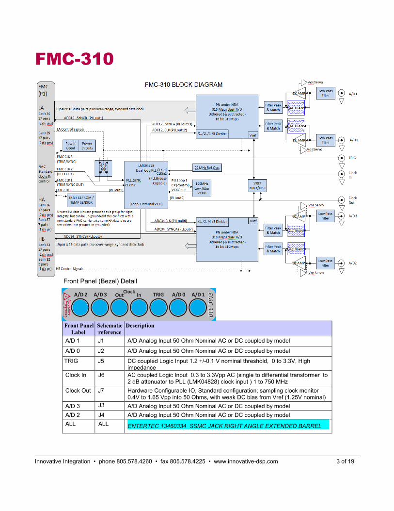
DC-Coupled A/D GAIN vs Frequency. Gain was measured with a 50 Ohm series terminated voltage source (see Notes).Gain with a zero impedance voltage source will increase approximately 6 dB
DC-Coupled A/D ISOLATION vs Frequency.Channels are in two groups of two [(0..1) and (2..3)] on opposte sides of the FMC-310 module. Adjacent channel isolation is measured within group, oppositechannel isolation is between groups (measurement SFDR limited)
Uncorrected DC Coupled A/D FFT Plots
DC-Coupled A/D with 5.1 MHz Input (SN B105 ch 0) DC-Coupled A/D with 30.1 MHz Input (SN B105 ch 3)
Innovative Integration • phone 805.578.4260 • fax 805.578.4225 • www.innovative-dsp.com 11 of 19
-3.5
-3
-2.5
-2
-1.5
-1
-0.5
0
0.5
10 50 100 150 200 250 300 350 400
Input Frequency (MHz)
Gain (dB)
0
20
40
60
80
100
120
0 100 200 300 400
Input Frequency (MHz)
Isolation (dB)
Adj. Chan
Opp. Chan

FMC-310
DC-Coupled A/D with 105.1 MHz Input (SN B105 ch 3) DC-Coupled A/D with 180.1 MHz Input (SN B105 ch 3)
Gain Definition
FMC-310 is specified and tested with a 50 Ohm source impedance (unless otherwise noted). The FMC-310 nominal gain isapproximately 1X or 0dB when calibrated, the voltage at the FMC-310 input equals the digital reading output. Internally theA/D IC sees about twice the voltage applied at the FMC-310 input but the FMC-310 is calibrated to its input in typical use.
Practically the 50 Ohm terminations in a RF system are rarely physical resistors (they are the Thévenin equivalent of thecircuit). At lower input frequencies 50 Ohm source terminations are not common but are needed for continuity with RF 50Ohm measurements. This source 50 Ohm series termination forms a voltage divider with the FMC-310 input impedancereducing the source voltage by approximately ½ at the FMC-310 input. A series 0 Ohm source resistance will change thecircuit gain by about 2X in Voltage or 6 dB. Variations in source impedance will change the system gain.
Digital Calibration Note
The FMC-310 can be digitally calibrated for offset and gain. However if the signal is clipped (outside the A/D range) theinformation is lost, so the raw gain is typically designed for a signal level at the A/D that is slightly less than A/D Full Scalein the bandwidth of interest to allow the nominal input range to be measured accurately without clipping when digitallycalibrated.
Bandwidth Notes
The standard DC coupled version targets maximum flatness and slightly less than 0 dB gain from DC to 90 MHz.
The standard AC coupled version targets broader band use, and a slightly lower gain in this band as the system gain willtypically be more variable due source impedance and level variation over frequency
Also slight gain peaking is present at high frequency to maximize BW and help compensate for likely cabling and filter roll-off in typical use.
Innovative Integration • phone 805.578.4260 • fax 805.578.4225 • www.innovative-dsp.com 12 of 19
FMC-310Powering
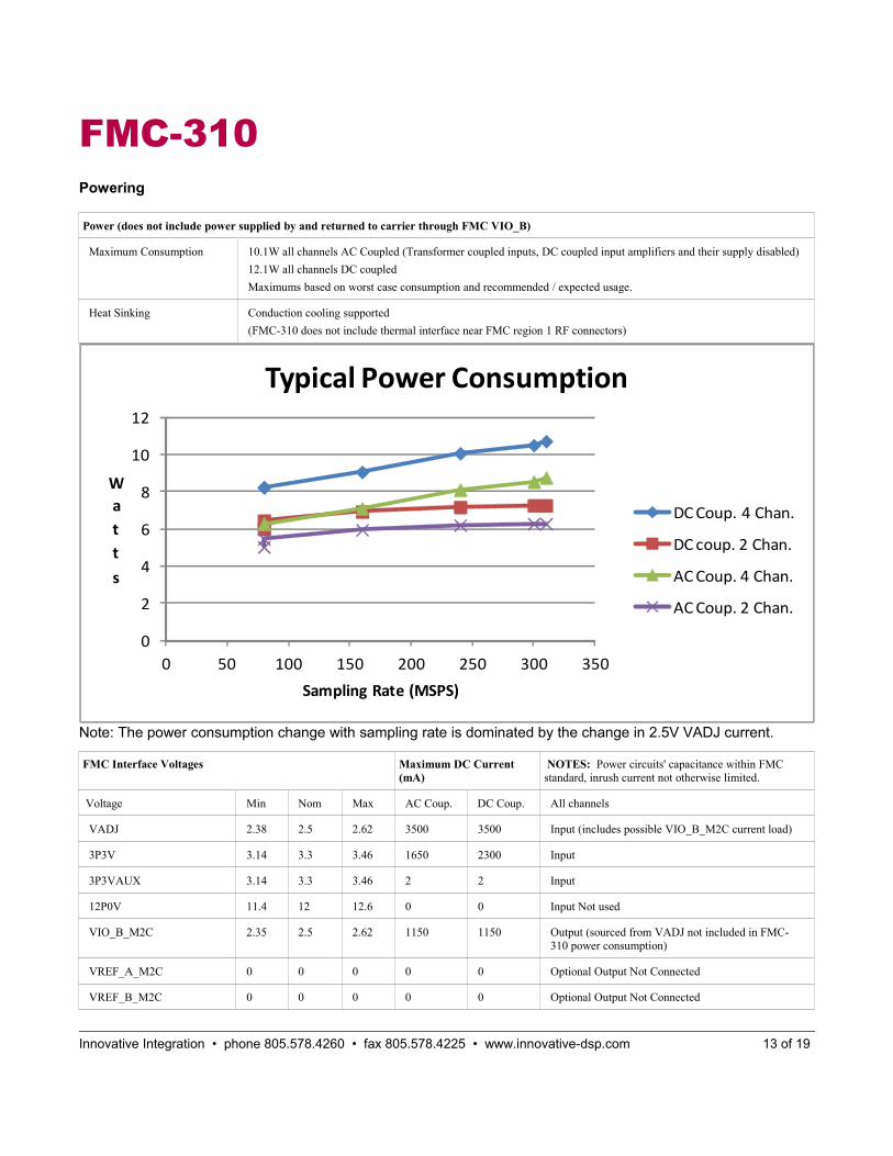
Power (does not include power supplied by and returned to carrier through FMC VIO_B)
Maximum Consumption 10.1W all channels AC Coupled (Transformer coupled inputs, DC coupled input amplifiers and their supply disabled)
12.1W all channels DC coupled
Maximums based on worst case consumption and recommended / expected usage.
Heat Sinking Conduction cooling supported
(FMC-310 does not include thermal interface near FMC region 1 RF connectors)
Note: The power consumption change with sampling rate is dominated by the change in 2.5V VADJ current.
FMC Interface Voltages Maximum DC Current (mA)
NOTES: Power circuits' capacitance within FMC standard, inrush current not otherwise limited.
Voltage Min Nom Max AC Coup. DC Coup. All channels
VADJ 2.38 2.5 2.62 3500 3500 Input (includes possible VIO_B_M2C current load)
3P3V 3.14 3.3 3.46 1650 2300 Input
3P3VAUX 3.14 3.3 3.46 2 2 Input
12P0V 11.4 12 12.6 0 0 Input Not used
VIO_B_M2C 2.35 2.5 2.62 1150 1150 Output (sourced from VADJ not included in FMC-310 power consumption)
VREF_A_M2C 0 0 0 0 0 Optional Output Not Connected
VREF_B_M2C 0 0 0 0 0 Optional Output Not Connected
Innovative Integration • phone 805.578.4260 • fax 805.578.4225 • www.innovative-dsp.com 13 of 19
0
2
4
6
8
10
12
0 50 100 150 200 250 300 350
Watts
Sampling Rate (MSPS)
Typical Power Consumption
DC Coup. 4 Chan.
DC coup. 2 Chan.
AC Coup. 4 Chan.
AC Coup. 2 Chan.

FMC-310Typical Measurement Notes:
Measurements were made with an approximately 91% FS (-0.82 dBFS) sinusoidal input, sampled at 310 MSPS,using the on-board PLL (Phase Locked Loop).
Measurements (except gain) used a narrow band pass filter (order 3 to 7, bandwidth 0.5 to 25 MHz) from thesignal generator (HP 8663A or R&S SMA100A) to the FMC-310 input.
Gain measurements are made in a 50 Ohm system, in this context the 50 Ohm series output termination of thetest source forms a voltage divider with the FMC-310 input impedance. Alternately when using a voltage sourcewithout a series termination, the Voltage gain will be approximately twice as big, and the above gain plot valuesare increased 6 dB for this. An un-terminated source is not practical at RF frequencies but is common at DC. Forcontinuity a series 50 Ohm source termination was used for low (and high) frequency gain measurements.
AC Gain measured with a 50 Ohm 10 dB attenuator (to improve signal generator return loss) and calibrated withan Agilent U2004A power sensor.
DC Gain measured with a 50 Ohm series resistor from a low noise Voltage source measured with a Fluke 179multimeter, opposite polarity measurements were made and subtracted to remove offset.
A 65536 point FFT (Fast Fourier Transform) with Blackman window was used. Signal level in raw FFT plots is notcorrected to dBFS (deciBel full scale). Input signal dBFS was set using the amplitude (from A/D counts).
SNR (and therefore ENOB calculated from SNR) measurements were corrected for filter bandwidth and bleedthrough. SNR measurements were corrected when the input noise contributed to the raw FFT SNR.
Harmonics were not corrected for filter bleed through (finite attenuation of test source harmonics in the filter stopbands), some of the above results are believed to be a few dB worse compared to double filtered measurements.
Isolation was measured with the victim channels' ports connected to a 50 Ohm termination through a cable.
The above test corrections were applied consistent with guidance from the A/D IC manufacturer for testequipment limitations. Some formulas for above test corrections taken from Analog Devices Tutorial MT-003 “Understand SINAD, SNR, THD, THD + N, and SFDR so You Don't Get Lost in the Noise Floor” by Walt Kester.
Innovative Integration • phone 805.578.4260 • fax 805.578.4225 • www.innovative-dsp.com 14 of 19
FMC-310FMC Connector
Innovative Integration • phone 805.578.4260 • fax 805.578.4225 • www.innovative-dsp.com 15 of 19

FMC-310K J H G F E D C B A
1 NC GND NC GND PG_M2C GND PG_C2M GND FMC_CLK_DIR
GND
2 GND FMC_CLK3_P GND FMC_CLK1_P GND FMC_HA01_P_CC
GND NC GND NC
3 GND FMC_CLK3_N GND FMC_CLK1_N GND FMC_HA01_N_CC
GND NC GND NC
4 FMC_CLK2_P GND FMC_CLK0_P GND FMC_HA00_P_CC
GND NC GND NC GND
5 FMC_CLK2_N GND FMC_CLK0_N GND FMC_HA00_N_CC
GND NC GND NC GND
6 GND FMC_HA03_P GND FMC_LA00_P_CC
ADC12_SYNB_P
GND FMC_HA05_P GND NC GND NC
7 FMC_HA02_P FMC_HA03_N FMC_LA02_P
ADC12_DATA_0_P
FMC_LA00_N_CC
ADC12_SYNB_N
FMC_HA04_P FMC_HA05_N GND NC GND NC
8 FMC_HA02_N GND FMC_LA02_N
ADC12_DATA_0_N
GND FMC_HA04_N GND FMC_LA01_P_CC
ADC12_DATA_CO_P
GND NC GND
9 GND FMC_HA07_P GND FMC_LA03_P
ADC12_DATA_1_P
GND FMC_HA09P
GND
FMC_LA01_N_CC
ADC12_DATA_CO_N
GND NC GND
10 FMC_HA06_P FMC_HA07_N FMC_LA04_P
ADC12_DATA_2_P
FMC_LA03_N
ADC12_DATA_1_N
FMC_HA08P
GND
FMC_HA09N
GND
GND FMC_LA06_P
ADC12_DATA_4_P
GND NC
11 FMC_HA06_N GND FMC_LA04_N
ADC12_DATA_2_N
GND FMC_HA08N
GND
GND FMC_LA05_P
ADC12_DATA_3_P
FMC_LA07_N
ADC12_DATA_4_N
GND NC
12 GND FMC_HA11P
GND
GND FMC_LA08_P
ADC12_DATA_6_P
GND FMC_HA13P
GND
MC_LA05_N
ADC12_DATA_3_N
GND NC GND
13 FMC_HA10_P
GND
FMC_HA11N
GND
FMC_LA07_P
ADC12_DATA_5_P
FMC_LA08_N
ADC12_DATA_6_N
FMC_HA12P
GND
FMC_HA13N
GND
GND GND NC GND
14 FMC_HA10_N
GND
GND FMC_LA07_N
ADC12_DATA_5_N
GND FMC_HA12N
GND
GND FMC_LA09_P
ADC12_DATA_7_P
FMC_LA10_P
ADC12_DATA_8_P
GND NC
15 GND FMC_HA14P
GND
GND FMC_LA12_P
ADC12_DATA_10_P
GND FMC_HA16P
GND
FMC_LA09_N
ADC12_DATA_7_N
FMC_LA10_N
ADC12_DATA_8_N
GND NC
16 FMC_HA17P_CC
GND
FMC_HA14N
GND
FMC_LA11_P
ADC12_DATA_9_P
FMC_LA12_N
ADC12_DATA_10N
FMC_HA15P
GND
FMC_HA16N
GND
GND GND NC GND
17 FMC_HA17N_CC
GND
GND FMC_LA11_N
ADC12_DATA_9_N
GND FMC_HA15N
GND
GND FMC_LA13_P
ADC12_DATA_11_P
GND NC GND
18 GND FMC_HA18P
GND
GND FMC_LA16_P
ADC12_DATA_14_P
GND FMC_HA20P
GND
FMC_LA713_N
ADC_DATA_11_N
FMC_LA14_P
ADC12_DATA_12_P
GND NC
19 FMC_HA21_P
GND
FMC_HA18N
GND
FMC_LA15_P
ADC12_DATA_13_P
FMC_LA16_N
ADC12_DATA_14_N
FMC_HA19P
GND
FMC_HA20N
GND
GND FMC_LA14_N
ADC12_DATA_12_N
GND NC
Innovative Integration • phone 805.578.4260 • fax 805.578.4225 • www.innovative-dsp.com 16 of 19

FMC-310K J H G F E D C B A
20 FMC_HA21_N
GND
GND FMC_LA15_N
ADC12_DATA_13N
GND FMC_HA19N
GND
GND FMC_LA17_P_CC
ADC12_DATA_15_P
GND NC GND
21 GND FMC_HA22P
GND
GND FMC_LA20P
ADC12_CSB
GND FMC_HB03_P
ADC34_DATA_2_P
FMC_LA17_N_CC
ADC12_DATA_15_N
GND NC GND
22 FMC_HA23_P
50_Ohm_Terminatio
FMC_HA22N
GND
FMC_LA19P
ADC12_SDI_CLK
FMC_LA20N
50 Ohm Termination
FMC_HB02_PADC34_DATA_1_P
FMC_HB03_N
ADC34_DATA_2_N
GND FMC_LA18_P_CC
ADC12_OVER-RANGE_P
GND NC
23 FMC_HA23_N
50_Ohm_Termination
GND FMC_LA19N
50_Ohm Termination
GND FMC_HB02_N
ADC34_DATA_1_N
GND FMC_LA23P
ADC1_FE_AMP_EN
FMC_LA18_N_CC
ADC12_OVER-RANGE_N
GND NC
24 GND FMC_HB01_P
ADC34_DATA_0_P
GND FMC_LA22P
ADC12_PWDN
GND FMC_HB05_P
ADC34_DATA_4_P
FMC_LA23N
ADC2_FE_AMP_EN
GND NC GND
25 FMC_HB00_P
ADC34_SYNB_P
FMC_HB01_N
ADC34_DATA_0_N
FMC_LA21P
ADC12_SDI_OUT
FMC_LA22N
ADC12_FE_AMP_PWR_EN
FMC_HB04_P
ADC34_DATA_3_P
FMC_HB05_N
ADC34_DATA_4_N
GND GND NC GND
26 FMC_HB00_N
ADC34_SYNB_N
GND FMC_LA21N
ADC12_SDI_IN
GND FMC_HBO4_N
ADC34_DATA_3_N
GND FMC_LA26P
FMC_TRIG/SYNC_OUT_SEL
FMC_LA27P
PLL_STATUS_1
GND NC
27 GND FMC_HB07_P
ADC34_DATA_5_P
GND FMC_LA25P
FMC_TEMP_ALERT
GND FMC_HB09_P
ADC34_DATA_7_P
FMC_LA26N
FMC_TRIG/SYNC_OUT_EN
FMC_LA27N
PLLSTATUS_2
GND NC
28 FMC_HB06_P
ADC34_DATA_CO_P
FMC_HB07_P
ADC34_DATA_5_N
FMC_LA24P
ADC3_FE_AMP_EN
FMC_LA25N
50_Ohm_Termination
FMC_HBB08_P
ADC34_DATA_6_P
FMC_HB09_N
ADC34_DATA_7_N
GND GND NC GND
29 FMC_HB06_N
ADC34_DATA_CO_N
GND FMC_LA24N
ADC4_FE_AMP_EN
GND FMC_HB08_N
ADC34_DATA_6_N
GND NC GND NC GND
30 GND FMC_HB11_P
ADC34_DATA_9_P
GND FMC_LA29P
PLL_STAT_3_C2M/M2C
GND FMC_HB13_P
ADC34_DATA_11_P
FMC_TDO FMC_SCL GND NC
31 FMC_HB10_P
ADC34_DATA_8_P
FMC_HB11_N
ADC34_DATA_9_N
FMC_LA28P
PLL_STATUS_3
FMC_LA29N_PLL_STAT_4_C2M/M2C
FMC_HB12_P
ADC34_DATA_10_P
FMC_HB13_N
ADC34_DATA_11_N
FMC_TDO FMC_SDA GND NC
32 FMC_HB10_N
ADC34_DATA_8_N
GND FMC_LA28N
PLL_STATUS_4
GND FMC_HB12_N
ADC34_DATA_10_N
GND 3P3VAUX GND NC GND
33 GND FMC_HB15_P
ADC34_DATA_13_P
GND FMC_LA31P
PLL_CS_N
GND FMC_HB19P
ADC34_SDI_CLK
NC GND NC GND
34 FMC_HB14_P
ADC34_DATA_12_P
FMC_HB15_N
ADC34_DATA_13_N
FMC_LA30P
PLL_RESET
FMC_LA31N
PLL_TRIG/SYNC_IN_SEL
FMC_HB16_P
ADC34_DATA_14_P
FMC_HB19P
ADC34_PWDN
NC GA0 GND NC
35 FMC_HB14_N
ADC34_DATA_12_N
GND FMC_LA30N
PLL_GPO
GND FMC_HB16_N
ADC34_DATA_14_N
GND GA1 12P0V GND NC
36 GND FMC_HB18_P
ADC34_OVER-RANGE_P
GND FMC_LA33P
PLL_SDI
GND FMC_HB21P
ADC34_SDI_OUT
3.3V GND NC GND
Innovative Integration • phone 805.578.4260 • fax 805.578.4225 • www.innovative-dsp.com 17 of 19
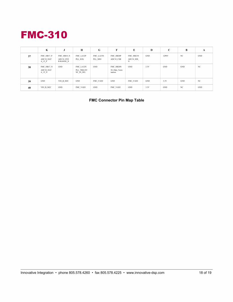
FMC-310K J H G F E D C B A
37 FMC_HB17_P
ADC34_DATA_15_P
FMC_HB18_N
ADC34_OVER-RANGE_N
FMC_LA32P
PLL_SCK
FMC_LA33N
PLL_SDO
FMC_HB20P
ADC34_CSB
FMC_HB21N
ADC34_SDI_N
GND 12P0V NC GND
38 FMC_HB17_N
ADC34_DATA_15_N
GND FMC_LA32N
PLL_TRIG/SYNC_IN_SEL
GND FMC_HB20N
50_Ohm_Termination
GND 3.3V GND GND NC
39 GND VIO_B_M2C GND FMC_VADJ GND FMC_VADJ GND 3.3V GND NC
40 VIO_B_M2C GND FMC_VADJ GND FMC_VADJ GND 3.3V GND NC GND
FMC Connector Pin Map Table
Innovative Integration • phone 805.578.4260 • fax 805.578.4225 • www.innovative-dsp.com 18 of 19

FMC-310
IMPORTANT NOTICESInnovative Integration Incorporated reserves the right to make corrections, modifications, enhancements, improvements, andother changes to its products and services at any time and to discontinue any product or service without notice. Customersshould obtain the latest relevant information before placing orders and should verify that such information is current andcomplete. All products are sold subject to Innovative Integration’s terms and conditions of sale supplied at the time of orderacknowledgment.
Innovative Integration warrants performance of its hardware products to the specifications applicable at the time of sale inaccordance with Innovative Integration’s standard warranty. Testing and other quality control techniques are used to theextent Innovative Integration deems necessary to support this warranty. Except where mandated by governmentrequirements, testing of all parameters of each product is not necessarily performed.
Innovative Integration assumes no liability for applications assistance or customer product design. Customers are responsiblefor their products and applications using Innovative Integration products. To minimize the risks associated with customerproducts and applications, customers should provide adequate design and operating safeguards.
Innovative Integration does not warrant or represent that any license, either express or implied, is granted under anyInnovative Integration patent right, copyright, mask work right, or other Innovative Integration intellectual property rightrelating to any combination, machine, or process in which Innovative Integration products or services are used. Informationpublished by Innovative Integration regarding third-party products or services does not constitute a license from InnovativeIntegration to use such products or services or a warranty or endorsement thereof. Use of such information may require alicense from a third party under the patents or other intellectual property of the third party, or a license from InnovativeIntegration under the patents or other intellectual property of Innovative Integration.
Reproduction of information in Innovative Integration data sheets is permissible only if reproduction is without alteration andis accompanied by all associated warranties, conditions, limitations, and notices. Reproduction of this information withalteration is an unfair and deceptive business practice.
Innovative Integration is not responsible or liable for such altered documentation. Resale of Innovative Integration productsor services with statements different from or beyond the parameters stated by Innovative Integration for that product orservice voids all express and any implied warranties for the associated Innovative Integration product or service and is anunfair and deceptive business practice. Innovative Integration is not responsible or liable for any such statements.
For further information on Innovative Integration products and support see our web site:
www.innovative-dsp.com
Mailing Address: Innovative Integration, Inc.
2390A Ward Avenue, Simi Valley, California 93065
Copyright ©2007, Innovative Integration, Incorporated
Innovative Integration • phone 805.578.4260 • fax 805.578.4225 • www.innovative-dsp.com 19 of 19