TPS65150 Low Input Voltage, Compact LCD Bias IC With ... - TI
49
V(VS) Boost Converter V(VGL) Negative Charge Pump V(CPI) Positive Charge Pump V(VGH) Gate-Voltage Shaping V(VCOM) VCOM Buffer Product Folder Order Now Technical Documents Tools & Software Support & Community An IMPORTANT NOTICE at the end of this data sheet addresses availability, warranty, changes, use in safety-critical applications, intellectual property matters and other important disclaimers. PRODUCTION DATA. TPS65150 SLVS576B – SEPTEMBER 2005 – REVISED JANUARY 2016 TPS65150 Low Input Voltage, Compact LCD Bias IC With VCOM Buffer 1 1 Features 1• 1.8-V to 6-V Input Voltage Range • Integrated VCOM Buffer • High-voltage Switch to Isolate V (VGH) • Gate-Voltage Shaping of V (VGH) • 2-A Internal MOSFET switch • Main Output V (VS) up to 15 V With <1% Output Voltage Accuracy • Virtual-Synchronous Converter Technology • Regulated Negative Charge Pump Driver V (VGL) • Regulated Positive Charge Pump Driver V (CPI) • Adjustable Power-On Sequencing • Adjustable Fault Detection Timing • Gate Drive Signal for External Isolation MOSFET • Out-of-Regulation Protection • Overvoltage Protection • Thermal Shutdown • Available in HTSSOP-24 Package • Available in VQFN-24 Package 2 Applications • TFT LCD Displays for Notebooks • TFT LCD Displays for Monitors • Car Navigation Displays 3 Description The TPS65150 device offers a very compact and small power supply solution that provides all three voltages required by thin film transistor (TFT) LCD displays. With an input voltage range of 1.8 V to 6 V the device is ideal for notebooks powered by a 2.5-V or 3.3-V input rail or monitor applications with a 5-V input voltage rail. Additionally the TPS65150 device provides an integrated high current buffer to provide the VCOM voltage for the TFT backplane. Two regulated adjustable charge pump driver provide the positive V (VGH) and negative V (VGL) bias voltages for the TFT. The device incorporates adjustable power-on sequencing for V (VGL) as well as for V (VGH) . This avoids any additional external components to implement application specific sequencing. The device has an integrated high-voltage switch to isolate V (VGH) . The same internal circuit can also be used to provide a gate shaping signal of V (VGH) for the LCD panel controlled by the signal applied to the CTRL input. For highest safety, the TPS65150 device has an integrated adjustable shutdown latch feature, which allows application-specific flexibility. The device monitors the outputs (V (VS) ,V (VGL) ,V (VGH) ); and, as soon as one of the outputs falls below its power good threshold, the device enters shutdown latch, after its adjustable delay time has passed by. Device Information (1) PART NUMBER PACKAGE BODY SIZE (NOM) TPS65150 HTSSOP (24) 7.80 mm × 4.40 mm VQFN (24) 4.00 mm × 4.00 mm (1) For all available packages, see the orderable addendum at the end of the data sheet. Block Diagram
Transcript of TPS65150 Low Input Voltage, Compact LCD Bias IC With ... - TI

V(VS)Boost
Converter
V(VGL)Negative
Charge Pump
V(CPI)Positive
Charge Pump
V(VGH)Gate-Voltage
Shaping
V(VCOM)VCOMBuffer
Product
Folder
Order
Now
Technical
Documents
Tools &
Software
Support &Community
An IMPORTANT NOTICE at the end of this data sheet addresses availability, warranty, changes, use in safety-critical applications,intellectual property matters and other important disclaimers. PRODUCTION DATA.
TPS65150SLVS576B –SEPTEMBER 2005–REVISED JANUARY 2016
TPS65150 Low Input Voltage, Compact LCD Bias IC With VCOM Buffer
1
1 Features1• 1.8-V to 6-V Input Voltage Range• Integrated VCOM Buffer• High-voltage Switch to Isolate V(VGH)
• Gate-Voltage Shaping of V(VGH)
• 2-A Internal MOSFET switch• Main Output V(VS) up to 15 V With <1% Output
Voltage Accuracy• Virtual-Synchronous Converter Technology• Regulated Negative Charge Pump Driver V(VGL)
• Regulated Positive Charge Pump Driver V(CPI)
• Adjustable Power-On Sequencing• Adjustable Fault Detection Timing• Gate Drive Signal for External Isolation MOSFET• Out-of-Regulation Protection• Overvoltage Protection• Thermal Shutdown• Available in HTSSOP-24 Package• Available in VQFN-24 Package
2 Applications• TFT LCD Displays for Notebooks• TFT LCD Displays for Monitors• Car Navigation Displays
3 DescriptionThe TPS65150 device offers a very compact andsmall power supply solution that provides all threevoltages required by thin film transistor (TFT) LCDdisplays. With an input voltage range of 1.8 V to 6 Vthe device is ideal for notebooks powered by a 2.5-Vor 3.3-V input rail or monitor applications with a 5-Vinput voltage rail. Additionally the TPS65150 deviceprovides an integrated high current buffer to providethe VCOM voltage for the TFT backplane.
Two regulated adjustable charge pump driver providethe positive V(VGH) and negative V(VGL) bias voltagesfor the TFT. The device incorporates adjustablepower-on sequencing for V(VGL) as well as for V(VGH).This avoids any additional external components toimplement application specific sequencing. Thedevice has an integrated high-voltage switch toisolate V(VGH).
The same internal circuit can also be used to providea gate shaping signal of V(VGH) for the LCD panelcontrolled by the signal applied to the CTRL input.For highest safety, the TPS65150 device has anintegrated adjustable shutdown latch feature, whichallows application-specific flexibility. The devicemonitors the outputs (V(VS), V(VGL), V(VGH)); and, assoon as one of the outputs falls below its power goodthreshold, the device enters shutdown latch, after itsadjustable delay time has passed by.
Device Information(1)
PART NUMBER PACKAGE BODY SIZE (NOM)
TPS65150HTSSOP (24) 7.80 mm × 4.40 mmVQFN (24) 4.00 mm × 4.00 mm
(1) For all available packages, see the orderable addendum atthe end of the data sheet.
Block Diagram

2
TPS65150SLVS576B –SEPTEMBER 2005–REVISED JANUARY 2016 www.ti.com
Product Folder Links: TPS65150
Submit Documentation Feedback Copyright © 2005–2016, Texas Instruments Incorporated
Table of Contents1 Features .................................................................. 12 Applications ........................................................... 13 Description ............................................................. 14 Revision History..................................................... 25 Pin Configuration and Functions ......................... 36 Specifications......................................................... 4
6.1 Absolute Maximum Ratings ...................................... 46.2 ESD Ratings.............................................................. 46.3 Recommended Operating Conditions....................... 56.4 Thermal Information .................................................. 56.5 Electrical Characteristics........................................... 56.6 Switching Characteristics .......................................... 76.7 Typical Characteristics .............................................. 8
7 Detailed Description ............................................ 107.1 Overview ................................................................. 107.2 Functional Block Diagram ....................................... 117.3 Feature Description................................................. 12
7.4 Device Functional Modes........................................ 218 Application and Implementation ........................ 23
8.1 Application Information............................................ 238.2 Typical Application ................................................. 238.3 System Examples ................................................... 32
9 Power Supply Recommendations ...................... 3510 Layout................................................................... 35
10.1 Layout Guidelines ................................................. 3510.2 Layout Example .................................................... 36
11 Device and Documentation Support ................. 3711.1 Device Support...................................................... 3711.2 Community Resources.......................................... 3711.3 Trademarks ........................................................... 3711.4 Electrostatic Discharge Caution............................ 3711.5 Glossary ................................................................ 37
12 Mechanical, Packaging, and OrderableInformation ........................................................... 37
4 Revision HistoryNOTE: Page numbers for previous revisions may differ from page numbers in the current version.
Changes from Revision A (March 2015) to Revision B Page
• Changed text in Negative Charge Pump Diodes section ..................................................................................................... 16• Changed text in Positive Charge Pump Diodes. section...................................................................................................... 18• Changed text in Choosing the Diodes and Choosing the Flying Capacitance sections ...................................................... 27• Changed text in Choosing the Diodes section .................................................................................................................... 28• Changed Figure 37 image .................................................................................................................................................... 36
Changes from Original (September 2005) to Revision A Page
• Added ESD Ratings table, Feature Description section, Device Functional Modes, Application and Implementationsection, Power Supply Recommendations section, Layout section, Device and Documentation Support section, andMechanical, Packaging, and Orderable Information section .................................................................................................. 1

1
2
3
4
5
6
7 8 9 10 11 12
18
17
16
15
14
13
Thermal Pad
24 23 22 21 20 19
COMP
GD
FDLY
FB
DLY1
DLY2
VIN
SW
SW
PG
ND
PG
ND
SU
P
VGH
ADJ
CTRL
FBP
IN
VCOM
FB
N
RE
F
GN
D
DR
VN
DR
VP
CP
I
FB
DLY1
DLY2
VIN
SW
SW
PGND
PGND
SUP
VCOM
IN
FBP
1
2
3
4
5
6
7
8
9
10
11
12
24
23
22
21
20
19
18
17
16
15
14
13
FDLY
GD
COMP
FBN
REF
GND
DRVN
DRVP
CPI
VGHADJ
CTRL
The
rmal
Pad
3
TPS65150www.ti.com SLVS576B –SEPTEMBER 2005–REVISED JANUARY 2016
Product Folder Links: TPS65150
Submit Documentation FeedbackCopyright © 2005–2016, Texas Instruments Incorporated
5 Pin Configuration and Functions
RGE Package24-Pin VQFN
Top View
PWP Package24-Pin HTSSOP
Top View
Pin FunctionsPIN
I/O DESCRIPTIONNAME VQFN HTSSOP
ADJ 17 14 I/O Gate voltage shaping circuit. Connecting a capacitor to this pin sets the fall timeof the positive gate voltage V(VGH).
COMP 1 22 O This is the compensation pin for the main boost converter. A small capacitor andif required a series resistor is connected to this pin.
CPI 19 16 I Input of the VGH isolation switch and gate voltage shaping circuit.
CTRL 16 13 I
Control signal for the gate voltage shaping signal. Apply the control signal for thegate voltage control. Usually the timing controller of the LCD panel generatesthis signal. If this function is not required, this pin must be connected to VI. Bydoing this, the internal switch between CPI and VGH provides isolation for thepositive charge pump output V(VGH). DLY2 sets the delay time for V(VGH) to comeup.
DLY1 5 2 I/OPower-on sequencing adjust. Connecting a capacitor from this pin to groundallows to set the delay time between the boost converter output V(VS) and thenegative charge pump V(VGL) during start-up.
DLY2 6 3 I/O
Power-on sequencing adjust. Connecting a capacitor from this pin to groundallows to set the delay time between the negative charge pump V(VGL) and thepositive charge pump during start-up. Note that Q5 in the gate voltage shapingblock only turns on when the positive charge pump is within regulation. (Thisprovides input-output isolation of V(VGH)).
DRVN 21 18 I/O Negative charge pump driver.DRVP 20 17 I/O Positive charge pump driver.FB 4 1 I Boost converter feedback sense input.FBN 24 21 I Negative charge pump feedback sense input.FBP 15 12 I Positive charge pump feedback sense input.
FDLY 3 24 I/O
Fault delay. Connecting a capacitor from this pin to VI sets the delay time fromthe point when one or more of the of the outputs V(VS), V(VGH), V(VGL) dropsbelow its power good threshold until the device shuts down. To restart thedevice, the input voltage must be cycled to ground. This feature can be disabledby connecting the FDLY pin to VI.
GD 2 23 IActive-low, open-drain output. This output is latched low when the boostconverter output is in regulation. This signal can be used to drive an externalMOSFET to provide isolation for V(VS).
GND 22 19 Analog ground.

4
TPS65150SLVS576B –SEPTEMBER 2005–REVISED JANUARY 2016 www.ti.com
Product Folder Links: TPS65150
Submit Documentation Feedback Copyright © 2005–2016, Texas Instruments Incorporated
Pin Functions (continued)PIN
I/O DESCRIPTIONNAME VQFN HTSSOP
IN 14 11 I Input of the VCOM buffer. If this pin is connected to ground, the VCOM buffer isdisabled.
PGND 10, 11 7, 8 Power ground.REF 23 20 O Internal reference output, typically 1.213 V.
SUP 12 9 I/O Supply pin of the positive, negative charge pump and boost converter gate drivecircuit. This pin should be connected to the output of the main boost converter.
SW 8, 9 5, 6 I Switch pin of the boost converter.VCOM 13 10 O VCOM buffer output. Typically a 1-µF output capacitor is required on this pin.
VGH 18 15 OPositive output voltage to drive the TFT gates with an adjustable fall time. Thispin is internally connected with a MOSFET switch to the positive charge pumpinput CPI.
VIN 7 4 I This is the input voltage pin of the device.Thermal Pad — — The thermal pad must to be soldered to GND
(1) Stresses beyond those listed under Absolute Maximum Ratings may cause permanent damage to the device. These are stress ratingsonly, and functional operation of the device at these or any other conditions beyond those indicated under Recommended OperatingConditions is not implied. Exposure to absolute-maximum-rated conditions for extended periods may affect device reliability.
(2) All voltage values are with respect to network ground terminal.
6 Specifications
6.1 Absolute Maximum Ratingsover operating free-air temperature range (unless otherwise noted) (1)
MIN MAX UNITVoltages on pin VIN (2) –0.3 7 VVoltages on pin SUP –0.3 15.5 VVoltage on pin SW 20 VVoltage on CTRL –0.3 7 VVoltage on GD 15.5 VVoltage on CPI 32 VContinuous power dissipation See Thermal Information —Lead temperature (soldering, 10 s) 260 °COperating junction temperature –40 150 °CStorage temperature –65 150 °C
(1) JEDEC document JEP155 states that 500-V HBM allows safe manufacturing with a standard ESD control process.(2) JEDEC document JEP157 states that 250-V CDM allows safe manufacturing with a standard ESD control process.
6.2 ESD RatingsVALUE UNIT
V(ESD) Electrostatic dischargeHuman-body model (HBM), per ANSI/ESDA/JEDEC JS-001 (1) ±2000
VCharged-device model (CDM), per JEDEC specification JESD22-C101 (2) ±500

5
TPS65150www.ti.com SLVS576B –SEPTEMBER 2005–REVISED JANUARY 2016
Product Folder Links: TPS65150
Submit Documentation FeedbackCopyright © 2005–2016, Texas Instruments Incorporated
(1) Refer to application section for further information.
6.3 Recommended Operating ConditionsMIN NOM MAX UNIT
VI Input voltage range 1.8 6 VVO Boost converter output voltage 15 VL Inductor (1) 4.7 µHTA Operating ambient temperature –40 85 °CTJ Operating junction temperature –40 125 °C
(1) For more information about traditional and new thermal metrics, see the Semiconductor and IC Package Thermal Metrics applicationreport, SPRA953.
6.4 Thermal Information
THERMAL METRIC (1)TPS65150
UNITPWP (HTSSOP) RGE (VQFN)24 PINS 24 PINS
RθJA Junction-to-ambient thermal resistance 36.4 34.3 °C/WRθJC(top) Junction-to-case (top) thermal resistance 18.8 36.2 °C/WRθJB Junction-to-board thermal resistance 15.9 12 °C/WψJT Junction-to-top characterization parameter 0.4 0.5 °C/WψJB Junction-to-board characterization parameter 15.7 12.1 °C/WRθJC(bot) Junction-to-case (bottom) thermal resistance 1.3 3.2 °C/W
6.5 Electrical CharacteristicsVI = 3.3 V, V(VS) = 10 V, TA = –40°C to 85°C, typical values are at TA = 25°C (unless otherwise noted)
PARAMETER TEST CONDITIONS MIN TYP MAX UNITSUPPLY CURRENTVI Input voltage (VIN) 1.8 6 V
Supply current (VIN) Device not switching 14 25 µASupply current (SUP) Device not switching 1.9 3 mASupply current (VCOM buffer) 750 1500 µA
VIT– Undervoltage lockout threshold (VIN) VI falling 1.6 1.8 VVIT+ Undervoltage lockout threshold (VIN) VI rising 1.7 1.9 V
Thermal shutdown temperaturethreshold TJ rising 155 °C
Thermal shutdown temperaturehysteresis 10 °C
LOGIC SIGNALSVIH High-level input voltage (CTRL) 1.6 VVIL Low-level input voltage (CTRL) 0.4 VIIH, IIL Input current (CTRL) CTRL = VI or GND 0.01 0.2 µABOOST CONVERTERVO Output voltage 15 VVref Boost converter reference voltage (FB) 1.136 1.146 1.154 VIIB Input bias current (FB) 10 100 nA
rDS(on) Drain-source on-state resistance (Q1) IDS = 500 mAVO = 10 V 200 300
mΩVO = 5 V 305 450
rDS(on) Drain-source on-state resistance (Q2) IDS = 500 mAVO = 10 V 8 15
ΩVO = 5 V 12 22
IDS Drain-source current rating (Q2) 1 ACurrent limit (SW) 2 2.5 3.4 A

6
TPS65150SLVS576B –SEPTEMBER 2005–REVISED JANUARY 2016 www.ti.com
Product Folder Links: TPS65150
Submit Documentation Feedback Copyright © 2005–2016, Texas Instruments Incorporated
Electrical Characteristics (continued)VI = 3.3 V, V(VS) = 10 V, TA = –40°C to 85°C, typical values are at TA = 25°C (unless otherwise noted)
PARAMETER TEST CONDITIONS MIN TYP MAX UNIT
(1) The GD signal is latched low when the main boost converter output is within regulation. The GD signal is reset when the voltage on theVIN pin goes below the UVLO threshold voltage..
(2) The maximum charge pump output current is half the drive current of the internal current source or sink.
I(SW)(off) Off-state current (SW) V(SW) = 15 V 1 10 µA
VIT+Overvoltage protection threshold(SUP) V(SUP) rising 16 20 V
ΔVO(ΔVI) Line regulation VI = 1.8 V to 5 V IO = 1 mA 0.007 %/VΔVO(ΔIO) Load regulation VI = 5 V IO = 0 A to 400 mA 0.16 %/A
VIT+ Gate drive threshold (FB) (1) –12%of Vref
–4% ofVref
V
NEGATIVE CHARGE PUMPVO Output voltage –2 VV(REF) Reference output voltage (REF) 1.205 1.213 1.219 VVref Feedback regulation voltage (FBN) –36 0 36 mVIIB Input bias current (FBN) 10 100 nArDS(on) Drain-source on-state resistance (Q4) IDS = 20 mA 4.4 Ω
V(DRVN) Current sink voltage drop (2) V(FBN) = 5% abovenominal voltage
I(DRVN) = 50 mA 130 300mV
I(DRVN) = 100 mA 280 450ΔVO(ΔIO) Load regulation VO = –5 V IO = 0 mA to 20 mA 0.016 %/mAPOSITIVE CHARGE PUMPVO Output voltage CTRL = GND VGH = open 30 VVref Feedback regulation voltage (FBP) CTRL = GND VGH = open 1.187 1.214 1.238 VIIB Input bias current (FBP) CTRL = GND VGH = open 10 100 nArDS(on) Drain-source on-state resistance (Q3) IDS = 20 mA 1.1 Ω
V(SUP) –V(DRVP)
Current sink voltage drop (2) V(FBP) = 5% belownominal voltage
I(DRVP) = 50 mA 420 650mV
I(DRVP)= 100 mA 900 1400ΔVO(ΔIO) Load regulation VO = 24 V IO = 0 mA to 20 mA 0.07 %/mAGATE-VOLTAGE SHAPINGrDS(on) Drain-source on-state resistance (Q5) IO = –20 mA 12 30 ΩI(ADJ) Capacitor charge current V(ADJ) = 20 V V(CPI) = 30 V 160 200 240 µAVOmin Minimum output voltage V(ADJ) = 0 V IO = –10 mA 2 VIOM Maximum output current 20 mATIMING CIRCUITS DLY1, DLY2, FDLY
I(DLY1)Drive current into delay capacitor(DLY1) V(DLY1) = 1.213 V 3 5 7 µA
I(DLY2)Drive current into delay capacitor(DLY1) V(DLY2) = 1.213 V 3 5 7 µA
R(FDLY) Fault time delay resistor 250 450 650 kΩGATE DRIVE (GD)VOL Low-level output voltage (GD) IOL = 500 µA 0.5 VIOH Off-state current (GD) VOH = 15 V 0.001 1 µAVCOM BUFFER
VISR Single-ended input voltage (IN) 2.25 V(SUP) –2 V V
VIO Input offset voltage (IN) IO = 0 mA –25 25 mV

7
TPS65150www.ti.com SLVS576B –SEPTEMBER 2005–REVISED JANUARY 2016
Product Folder Links: TPS65150
Submit Documentation FeedbackCopyright © 2005–2016, Texas Instruments Incorporated
Electrical Characteristics (continued)VI = 3.3 V, V(VS) = 10 V, TA = –40°C to 85°C, typical values are at TA = 25°C (unless otherwise noted)
PARAMETER TEST CONDITIONS MIN TYP MAX UNIT
ΔVO(ΔIO) Load regulation
IO = ±25 mA –37 37
mVIO = ±50 mA –77 55IO = ±100 mA –85 85IO = ±150 mA –110 110
IIB Input bias current (IN) –300 –30 300 nA
IOM Maximum output current (VCOM)V(SUP) = 15 V 1.2
AV(SUP) = 10 V 0.65V(SUP) = 5 V 0.15
6.6 Switching Characteristicsover operating free-air temperature range (unless otherwise noted)
PARAMETER TEST CONDITIONS MIN TYP MAX UNITOscillator frequency 1.02 1.2 1.38 MHzDuty cycle (DRVN) 50%Duty cycle (DRVP) 50%

1.18
1.19
1.20
1.21
1.22
1.23
1.24
−40 −20 0 20 40 60 80 100 120Junction Temperature (°C)
Vol
tage
(V
)
G000
1.200
1.205
1.210
1.215
1.220
−40 −20 0 20 40 60 80 100 120Junction Temperature (°C)
Vol
tage
(V
)
G000
0
5
10
15
20
25
−40 −20 0 20 40 60 80 100 120Junction Temperature (°C)
Res
ista
nce
(Ω)
G000
1.135
1.140
1.145
1.150
1.155
−40 −20 0 20 40 60 80 100 120Junction Temperature (°C)
Vol
tage
(V
)
G000
2.0
2.2
2.4
2.6
2.8
3.0
3.2
3.4
−40 −20 0 20 40 60 80 100 120Junction Temperature (°C)
Cur
rent
(A
)
G000
0.00
0.05
0.10
0.15
0.20
0.25
0.30
−40 −20 0 20 40 60 80 100 120Junction Temperature (°C)
Res
ista
nce
(Ω)
G000
8
TPS65150SLVS576B –SEPTEMBER 2005–REVISED JANUARY 2016 www.ti.com
Product Folder Links: TPS65150
Submit Documentation Feedback Copyright © 2005–2016, Texas Instruments Incorporated
6.7 Typical Characteristics
Figure 1. Boost Converter Switch (Q1) Current Limit Figure 2. Boost Converter Switch (Q1) rDS(on) vsTemperature
Figure 3. Boost Converter Rectifier (Q2) rDS(on) vsTemperature
Figure 4. Boost Converter Reference Voltage vsTemperature
Figure 5. Positive Charge Pump Reference Voltage vsTemperature
Figure 6. REF Pin Voltage vs Temperature

1.00
1.05
1.10
1.15
1.20
1.25
1.30
1.35
1.40
−40 −20 0 20 40 60 80 100 120Junction Temperature (°C)
Fre
quen
cy (
MH
z)
G000
9
TPS65150www.ti.com SLVS576B –SEPTEMBER 2005–REVISED JANUARY 2016
Product Folder Links: TPS65150
Submit Documentation FeedbackCopyright © 2005–2016, Texas Instruments Incorporated
Typical Characteristics (continued)
Figure 7. Oscillator Frequency vs Temperature
10
TPS65150SLVS576B –SEPTEMBER 2005–REVISED JANUARY 2016 www.ti.com
Product Folder Links: TPS65150
Submit Documentation Feedback Copyright © 2005–2016, Texas Instruments Incorporated
7 Detailed Description
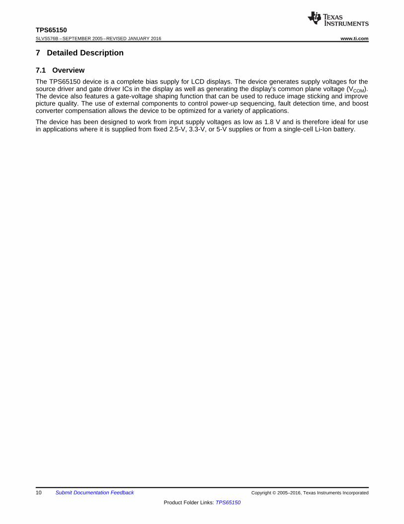
7.1 OverviewThe TPS65150 device is a complete bias supply for LCD displays. The device generates supply voltages for thesource driver and gate driver ICs in the display as well as generating the display's common plane voltage (VCOM).The device also features a gate-voltage shaping function that can be used to reduce image sticking and improvepicture quality. The use of external components to control power-up sequencing, fault detection time, and boostconverter compensation allows the device to be optimized for a variety of applications.
The device has been designed to work from input supply voltages as low as 1.8 V and is therefore ideal for usein applications where it is supplied from fixed 2.5-V, 3.3-V, or 5-V supplies or from a single-cell Li-Ion battery.

&Boost converter soft start completed
V(FB) power good
Disable
+
±
V(SUP)
Q11
Q12
Soft Start
5 µA1.213 V delay 1
V(SUP)
Current Control
&Soft Start
DLY1
DLY2
DRVN
FBN
I(DRVN)
V(SUP)
Current Control
&Soft Start
DRVP
FBP
I(DRVP)
1.214 V
Q4
Q3
+
± SawtoothGenerator
COMP
FB
Control Logic
&Gate
Drivers
V(VIN)
Q1
PGND
Current Limit
&SoftStart
SW
1.2 MHz
ControlLogic
200 µA
VGH
CPI
ADJ
Q5
Q6
Q7
GD
VCOM
REF
1.213 V delay 25 µA
+
±
+
±
1.146 V
IN
1.2 MHz
1.2 MHz
SUP
CTRL
UVLOV(FBP) power good &
References,Control Logic,
Oscillator,Sequencing,
Fault Detection &Thermal Shutdown
VIN
FDLY
fault0.69VI
GND
1.2 MHz
450 k
1.213 V
1.146 V
Q2
11
TPS65150www.ti.com SLVS576B –SEPTEMBER 2005–REVISED JANUARY 2016
Product Folder Links: TPS65150
Submit Documentation FeedbackCopyright © 2005–2016, Texas Instruments Incorporated
7.2 Functional Block Diagram

D = 1 ± VI
VO
VO
CO
Q1
R1
R2
SUP
FB
+
±
Vref = 1.146 V
GateDrive
Current Limit & Soft Start
SW
Q2
COMP
SawtoothGenerator
VIN
1.2 MHz
VI
RCOMP
CCOMP
L
CFF
CI
I(SW)
To charge pumps, VCOM
buffer, etc.
Feed-forward signal
Copyright © 2016, Texas Instruments Incorporated
12
TPS65150SLVS576B –SEPTEMBER 2005–REVISED JANUARY 2016 www.ti.com
Product Folder Links: TPS65150
Submit Documentation Feedback Copyright © 2005–2016, Texas Instruments Incorporated
7.3 Feature Description
7.3.1 Boost ConverterFigure 8 shows a simplified block diagram of the boost converter.
Figure 8. Boost Converter Block Diagram
The boost converter uses a unique fast-response voltage-mode controller scheme with input feedforward toachieve excellent line and load regulation, while still allowing the use of small external components. The use ofexternal compensation adds flexibility and allows the boost converter's response to be optimized for a wide rangeof external components.
The TPS65150 device uses a virtual-synchronous topology that allows the boost converter to operate incontinuous conduction mode (CCM) even at light loads. This is achieved by including a small MOSFET (Q2) inparallel with the external rectifier diode. Under light-load conditions, Q2 allows the inductor current to becomenegative, maintaining operation in CCM. By operating always in CCM, boost converter compensation issimplified, ringing on the SW pin at low loads is avoided, and additional charge pump stages can be driven bythe SW pin. The boost converter duty cycle is given by Equation 1.
WHITESPACE
where• η is the boost converter efficiency (either taken from data in Application Curves or a worst-case assumption of
75%).• VI is the boost converter input supply voltage.

PD = VFIO
IFRM = I:SW;M
VO = l1 + R1
R2pVref
I:SW;M = DVI
2fL +
IO1 ± D
13
TPS65150www.ti.com SLVS576B –SEPTEMBER 2005–REVISED JANUARY 2016
Product Folder Links: TPS65150
Submit Documentation FeedbackCopyright © 2005–2016, Texas Instruments Incorporated
Feature Description (continued)• VO is the boost converter output voltage. (1)
WHITESPACE
Use Equation 2 to calculate the boost converter peak switch current.
WHITESPACE
where• f = 1.2 MHz (the boost converter switching frequency);• IO is the boost converter output current; and• L is the boost converter inductance. (2)
WHITESPACE
7.3.1.1 Setting the Boost Converter Output VoltageThe boost converter output voltage is set by the R1/R2 resistor divider, and is calculated using Equation 3.
WHITESPACE
where• Vref = 1.146 V (the boost converter internal reference voltage). (3)
WHITESPACE
To minimize quiescent current consumption, the value of R1 should be in the range of 100 kΩ to 1 MΩ.
7.3.1.2 Boost Converter Rectifier DiodeThe diode's reverse voltage rating should be higher than the maximum output voltage of the converter, and itsaverage forward current rating should be higher than the boost converter's output current. Use Equation 4 tocalculate the rectifier diode repetitive peak forward current.
WHITESPACE
(4)
WHITESPACE
Use Equation 5 to calculate the power dissipated in the rectifier diode.
WHITESPACE
where• VF is the rectifier diode forward voltage. (5)
WHITESPACE
The main diode parameters affecting converter efficiency are its forward voltage and reverse leakage current,and both should be as low as possible.
7.3.1.3 Choosing the Boost Converter Output CapacitanceThe boost converter's output capacitance smooths the output voltage and supplies transient output currentdemands that are outside the converter's loop bandwidth. Generally speaking, larger output currents and/orsmaller input supply voltages require larger output capacitances. Use Equation 6 to calculate the boostconverter's output voltage ripple.
WHITESPACE

fco = 1
:R1;CFF
VO:PP; = DIOfCO
14
TPS65150SLVS576B –SEPTEMBER 2005–REVISED JANUARY 2016 www.ti.com
Product Folder Links: TPS65150
Submit Documentation Feedback Copyright © 2005–2016, Texas Instruments Incorporated
Feature Description (continued)
where• CO is the boost converter output capacitance. (6)
WHITESPACE
7.3.1.4 CompensationThe boost converter requires a series R-C network connected between the COMP pin and ground tocompensate its feedback loop. The COMP pin is the output of the boost converter's error amplifier, and thecompensation capacitor determines the amplifier's low-frequency gain and the resistor its high-frequency gain.Because the converter gain changes with the input voltage, different compensation capacitors may be required:lower input voltages require a higher gain, and therefore a smaller compensation capacitor value. If anapplication's input supply voltage changes (for example, if the TPS65150 device is supplied from a battery),choose compensation components suitable for a supply voltage midway between the minimum and maximumvalues. In all cases, verify that the values selected are suitable by performing transient tests over the full range ofoperating conditions.
Table 1. Recommended Compensation Components for Different Input Supply Voltages
VI CCOMP RCOMPFEED-FORWARD ZEROCUT-OFF FREQUENCY
2.5 V 470 pF 68 kΩ 8.8 kHz3.3 V 470 pF 33 kΩ 7.8 kHz5 V 2.2 nF 0 kΩ 11.2 kHz
A feed-forward capacitor CFF in parallel with the upper feedback resistor R1 adds an additional zero to the loopresponse, which improves transient performance. Table 1 suggests suitable values for the cut-off frequency ofthe feedforward zero; however, these are only guidelines. In any application, variations in input supply voltage,inductance, and output capacitance all affect circuit operation, and the optimum value must be verified withtransient tests before being finalized.
The cut-off frequency of the feed-forward zero is determined using Equation 7.
WHITESPACE
where• fco is the cutoff frequency of the feedforward zero formed by R1 and CFF. (7)
WHITESPACE
7.3.1.5 Soft StartThe boost converter features a soft-start function that limits the current drawn from the input supply during start-up. During the first 2048 switching cycles, the boost converter's switch current is limited to 40% of its maximumvalue; during the next 2048 cycles, it is limited to 60% of its maximum value; and after that it is as high as it mustbe to regulate the output voltage (up to 100% of the maximum). In typical applications, this results in a start-uptime of about 5 ms (see Figure 9).

VO
COI(DRVN)
Q4
R1
R2
CFLY
SUP
DRVN
FBN+
±
Current Control
&Soft Start
REF
+
±
1.213 V
D1
D2
1.2 MHz
Copyright © 2016, Texas Instruments Incorporated
40%
t2048 cyclest t2048 cyclest
60%
100%
0%
t
Sw
itch
Cur
rent
Lim
it
15
TPS65150www.ti.com SLVS576B –SEPTEMBER 2005–REVISED JANUARY 2016
Product Folder Links: TPS65150
Submit Documentation FeedbackCopyright © 2005–2016, Texas Instruments Incorporated
Figure 9. Boost Converter Switch Current Limit During Soft-Start
7.3.1.6 Gate Drive SignalThe GD pin provides a signal to control an external P-channel enhancement MOSFET, allowing the boostconverter's output to be isolated from its input when disabled (see Figure 36). The GD pin is an open-drain typewhose output is latched low as soon as the boost converter's output voltage reaches its power-good threshold.The GD pin goes high impedance whenever the input voltage falls below the undervoltage lockout threshold orthe device shuts down as the result of a fault condition (see Adjustable Fault Delay).
7.3.2 Negative Charge PumpFigure 10 shows a simplified block diagram of the negative charge pump.
Figure 10. Negative Charge Pump Block Diagram

VO(PP) = IO
2fCO
VO = ± lR1
R2pV(REF)
16
TPS65150SLVS576B –SEPTEMBER 2005–REVISED JANUARY 2016 www.ti.com
Product Folder Links: TPS65150
Submit Documentation Feedback Copyright © 2005–2016, Texas Instruments Incorporated
The negative charge pump operates with a fixed frequency of 1.2 MHz and a 50% duty cycle in two distinctphases. During the charge phase, transistor Q4 is turned on, controlled current source I(DRVN) is turned off, andflying capacitance CFLY charges up to approximately V(SUP). During the discharge phase, Q4 is turned off, I(DRVN)is turned on, and a negative current of I(DRVN) flows through D1 to the output. The output voltage is fed backthrough R1 and R2 to an error amplifier that controls I(DRVN) so that the output voltage is regulated at the correctvalue.
7.3.2.1 Negative Charge Pump Output VoltageThe negative charge pump output voltage is set by resistors R1 and R2 and is given by
WHITESPACE
where• V(REF) = 1.213 V (the voltage on the REF pin). (8)
WHITESPACE
Resistor R2 should be in the range 39 kΩ to 150 kΩ. Smaller values load the REF pin too heavily and largervalues may cause stability problems.
7.3.2.2 Negative Charge Pump Flying CapacitanceThe flying capacitance transfers charge from the SUP pin to the negative charge pump output. TI recommends aflying capacitance of at least 100 nF for output currents up to 20 mA. Smaller values can be used with smalleroutput currents.
7.3.2.3 Negative Charge Pump Output CapacitanceThe output capacitance smooths the discontinuous current delivered by the flying capacitance to generate a dcoutput voltage. In general, higher output currents require larger output capacitances. Use Equation 9 to calculatethe negative charge pump output voltage ripple.
WHITESPACE
where• IO is the negative charge pump output current.• CO is the negative charge pump output capacitance.• f = 1.2 MHz (the negative charge pump switching frequency). (9)
7.3.2.4 Negative Charge Pump DiodesThe average forward current of both diodes is equal to the negative charge pump output current. If therecommended flying capacitance (or larger) is used, the repetitive peak forward current in D1 and D2 is equal totwice the output current.
7.3.3 Positive Charge PumpFigure 11 shows a simplified block diagram of the positive charge pump, which works in a similar way to thenegative charge pump except that the positions of the current source IDRVP and the MOSFET Q3 are reversed.

VO(PP) = IO
2fCO
VO = l1 + R1
R2pVref
V(VS)
VO
CO
I(DRVP)
Q3
R1
R2
CFLY
SUP
DRVP
FBP
+
±
Vref = 1.214 V
Current Control
&Soft Start
D2
D1
1.2 MHz
Copyright © 2016, Texas Instruments Incorporated
17
TPS65150www.ti.com SLVS576B –SEPTEMBER 2005–REVISED JANUARY 2016
Product Folder Links: TPS65150
Submit Documentation FeedbackCopyright © 2005–2016, Texas Instruments Incorporated
(1) The minimum recommended flying capacitance for the positive charge pump is larger than for the negative charge pump because therDS(on) of Q3 is smaller than the rDS(on) of Q4.
Figure 11. Positive Charge Pump Block Diagram
If higher output voltages are required another charge pump stage can be added to the output, as shown inFigure 34 at the end of the data sheet.
7.3.3.1 Positive Charge Pump Output VoltageThe positive charge pump output voltage is set by resistors R1 and R2 and is calculated using Equation 10:
WHITESPACE
where• Vref = 1.214 V (the positive charge pump reference voltage). (10)
WHITESPACE
TI recommends choosing a value for R2 not greater than 1 MΩ.
7.3.3.2 Positive Charge Pump Flying CapacitanceThe flying capacitance transfers charge from the SUP pin to the charge pump output. TI recommends a flyingcapacitance of at least 330 nF (1) for output currents up to 20 mA. Smaller values can be used with smalleroutput currents.
7.3.3.3 Positive Charge Pump Output CapacitanceThe positive charge pump output voltage ripple is given by
WHITESPACE
where• IO is the positive charge pump output current.• CO is the positive charge pump output capacitance.• f = 1.2 MHz (the positive charge pump switching frequency). (11)

td(DLY1) = CDLY1Vref
I(DLY1) and td(DLY2) =
CDLY2Vref
I(DLY2)
VI
V(VS)
V(VGL)
V(CPI)
V(GD)
VIT+ VIT±
Notes1. The fall times of V(VS), V(VGL), V(CPI) depend on their respective load currents and feedback resistances.
See note 1
ttd(DLY1)t
ttd(DLY2)t
V(VCOM)
18
TPS65150SLVS576B –SEPTEMBER 2005–REVISED JANUARY 2016 www.ti.com
Product Folder Links: TPS65150
Submit Documentation Feedback Copyright © 2005–2016, Texas Instruments Incorporated
WHITESPACE
7.3.3.4 Positive Charge Pump DiodesThe average forward current of both diodes is equal to the positive charge pump output current. If therecommended flying capacitance (or larger) is used, the repetitive peak forward current in D1 and D2 equal totwice output current.
7.3.4 Undervoltage LockoutAn undervoltage lockout (UVLO) function inhibits the TPS65150 device if the input supply voltage is too low forproper operation. The UVLO function senses the voltage on the VIN.
7.3.5 Power-On Sequencing, DLY1, DLY2The boost converter starts as soon as the input supply voltage exceeds the rising UVLO threshold. The negativecharge pump starts td(DLY1) seconds after the boost converter output voltage has reached its final value, and thepositive charge pump starts td(DLY2) seconds after the negative charge pump's output has reached its final value.The VCOM buffer starts up as soon as the positive charge pump's output voltage (V(CPI)) has reached its finalvalue.
Delay times td(DLY1) and td(DLY2) are set by capacitors connected between the DLY1 and DLY2 pins and ground.
Figure 12. Start-Up Sequencing With CTRL = H
The delay times td(DLY1) and td(DLY2) are set by the capacitors connected to the DLY1 and DLY2 pins respectively.Each of these pins is connected to its own 5-µA current source (I(DLY1) and I(DLY2)) that causes the voltage on theexternal capacitor to ramp up linearly. The delay time is defined by how long it takes the voltage on the externalcapacitor to reach the reference voltage, and is given by
where• Vref = 1.213 V (the internal reference voltage);• I(DLY1) = 5 µA (the DLY1 pin output current); and

CADJ
V(VIN) > VIT
ControlLogic
I(ADJ) = 200 µA
CTRL
VGH
CPI
ADJ
Q5
Q6
Q7
V(FBP) power good
&
Copyright © 2016, Texas Instruments Incorporated
V(VGH)(PP) = I(ADJ)tw(CTRL)
CADJ
19
TPS65150www.ti.com SLVS576B –SEPTEMBER 2005–REVISED JANUARY 2016
Product Folder Links: TPS65150
Submit Documentation FeedbackCopyright © 2005–2016, Texas Instruments Incorporated
• I(DLY2) = 5 µA (the DLY2 pin output current). (12)
7.3.6 Gate Voltage ShapingThe gate voltage shaping function can be used to reduce crosstalk between LCD pixels by reducing the gatedrivers’ input supply voltage between lines. Figure 13 shows a simplified block diagram of the gate voltageshaping function. Gate voltage shaping is controlled by a logic-level signal applied to the CTRL pin. When CTRLis high, Q5 and Q7 are on and Q6 is off, and the output of the positive charge pump is connected to the VGHpin. When CTRL is low, Q5 and Q7 are off and Q6 is on. Q6 operates as a source follower and tracks thevoltage on the ADJ pin, which ramps down linearly as the current sink I(ADJ) discharges external capacitor CADJ(see Figure 14). The peak-to-peak voltage on the VGH pin is determined by the value of CADJ and the duration ofthe low level applied to the CTRL pin, and is calculated using Equation 13.
WHITESPACE
where• I(ADJ) = 200 µA (ADJ pin output current)• tw(CTRL) is the duration of the low-level signal connected to the CTRL pin• CADJ is the capacitance connected to the ADJ pin (13)
WHITESPACE
When the input supply voltage is below the UVLO threshold or the device enters a shutdown condition becauseof a fault on one or more of its outputs, Q5 and Q6 turn off and the VGH pin is high impedance.
Figure 13. Gate Voltage Shaping Block Diagram

td(FDLY) = R(FDLY)CFDLY
CTRL
V(VGH)
V(CPI)
V(VGH)(PP)
ttw(CTRL)t
20
TPS65150SLVS576B –SEPTEMBER 2005–REVISED JANUARY 2016 www.ti.com
Product Folder Links: TPS65150
Submit Documentation Feedback Copyright © 2005–2016, Texas Instruments Incorporated
Figure 14. Gate Voltage Shaping Timing
7.3.7 VCOM BufferThe VCOM Buffer is a transconductance amplifier designed to drive capacitive loads. The IN pin is the input ofthe VCOM buffer. The VCOM buffer features a soft-start function that reduces the current drawn from the SUPpin when the amplifier starts up.
If the VCOM buffer is not required for certain applications, it is possible to shut down the VCOM buffer byconnecting IN to ground, reducing the overall quiescent current. The IN pin cannot be pulled dynamically toground during operation.
7.3.8 Protection
7.3.8.1 Boost Converter Overvoltage ProtectionThe boost converter features an overvoltage protection function that monitors the voltage on the SUP pin andforces the TPS65150 device to enter fault mode if the boost converter output voltage exceeds the overvoltagethreshold.
7.3.8.2 Adjustable Fault DelayThe TPS65150 device detects a fault condition and shuts down if the boost converter output or either of thecharge pump outputs falls out of regulation for longer than the fault delay time td(FDLY). Fault conditions aredetected by comparing the voltage on the feedback pins with the internal power-good thresholds. Outputs thatfall below their power-good threshold but recover within less than td(FDLY) seconds are not detected as faults andthe device does not shut down in such cases. The output fault detection function is active during start-up, so thedevice will shut down if any of its outputs fails to reach its power-good threshold during start-up. Shut-downfollowing an output voltage fault is a latched condition, and the input supply voltage must be cycled to recovernormal operation after it occurs.
The fault detection delay time is set by the capacitor connected between the FDLY and VIN pins and is given by
WHITESPACE
where• R(FDLY) = 450 kΩ (the internal resistance connected to the FDLY pin).• CFDLY is the external capacitance connected to the FDLY pin. (14)
WHITESPACE

100u
1m
10m
100m
1
1n 10n 100n 1uCapacitance Connected to FDLY Pin (F)
Fau
lt D
elay
Tim
e (s
)
MinimumTypicalMaximum
G000
21
TPS65150www.ti.com SLVS576B –SEPTEMBER 2005–REVISED JANUARY 2016
Product Folder Links: TPS65150
Submit Documentation FeedbackCopyright © 2005–2016, Texas Instruments Incorporated
Figure 15. Adjustable Fault Delay Time
7.3.8.3 Thermal ShutdownA thermal shutdown is implemented to prevent damage because of excessive heat and power dissipation.Typically, the thermal shutdown threshold is 155°C. When this threshold is reached, the device enters shutdown.The device can be enabled again by cycling the input supply voltage.
7.3.8.4 Undervoltage LockoutThe TPS65150 device has an undervoltage lockout (UVLO) function. The UVLO function stops device operationif the voltage on the VIN pin is less than the UVLO threshold voltage. This makes sure that the device onlyoperates when the supply voltage is high enough for correct operation.
7.4 Device Functional ModesThe TPS65150 device's functional modes are illustrated in Figure 16.
7.4.1 VI > VIT+
When the input supply voltage is above the undervoltage lockout threshold, the device is on and all its functionsare enabled. Note that full performance may not be available until the input supply voltage exceeds the minimumvalue specified in Recommended Operating Conditions.
7.4.2 VI < VIT–
When the input supply voltage is below the undervoltage lockout threshold, the TPS65150 device is off and all itsfunctions are disabled.
7.4.3 Fault ModeThe TPS65150 device immediately enters fault mode when any of the following is detected:• boost converter overvoltage• overtemperature
The TPS65150 device also enters fault mode if any of the following conditions is detected and persists for longerthan td(FDLY):• boost converter output out of regulation• negative charge pump output out of regulation• positive charge pump output out of regulation
The TPS65150 device does not function during fault mode. Cycle the input supply voltage to exit fault mode andrecover normal operation.
WHITESPACE

FAULT
DETECTION
ON
OFF
FAULT
ANY
STATE
VI < VIT±
Boost converter out of regulationNegative charge pump out of regulationPositive charge pump out of regulation
Fault condition duration longer than td(FDLY)
Thermal shutdownBoost converter over-voltage
Fault condition duration less than td(FDLY)
VI > VIT+
22
TPS65150SLVS576B –SEPTEMBER 2005–REVISED JANUARY 2016 www.ti.com
Product Folder Links: TPS65150
Submit Documentation Feedback Copyright © 2005–2016, Texas Instruments Incorporated
Device Functional Modes (continued)
Figure 16. Functional Modes
VIN SW
FB
SUP
DRVP
FBP
CPI
VGH
VCOM
VI FDLY
COMP
ADJ
DLY1
DLY2
100 nF
2.2 nF
22 pF
10 nF
10 nF
DRVN
FBN
REF
C7330 nF
C3330 nF
R3620 k
R4150 k
R275 k
R1820 k
C222 µF
C141 µF
C1522 pF
C16330 nF
C4330 nF R5
1 M
R656 k
C51 µF
C122 µF
L13.9 µH
CTRL
R8500 k
R7500 k
C61 nF
IN
PGND GND
V(VGH)
23 V, 20 mA
V(VCOM)
V(VS)
13.5 V, 450 mAVI
5 V
V(VGL)
±5 V, 20 mA
V(VS)
FLK
C8220 nF
D4
D5
D3
D2
C13
C9
C10
C11
C12GD
D1
Copyright © 2016, Texas Instruments Incorporated
23
TPS65150www.ti.com SLVS576B –SEPTEMBER 2005–REVISED JANUARY 2016
Product Folder Links: TPS65150
Submit Documentation FeedbackCopyright © 2005–2016, Texas Instruments Incorporated
8 Application and Implementation
NOTEInformation in the following applications sections is not part of the TI componentspecification, and TI does not warrant its accuracy or completeness. TI’s customers areresponsible for determining suitability of components for their purposes. Customers shouldvalidate and test their design implementation to confirm system functionality.
8.1 Application InformationThe TPS65150 device has been designed to provide the input supply voltages for the source drivers and gatedrivers plus the voltage for the common plane in LCD display applications. In addition, the device provides a gatevoltage shaping function that can be used to modulate the gate drivers' positive supply to reduce image sticking.
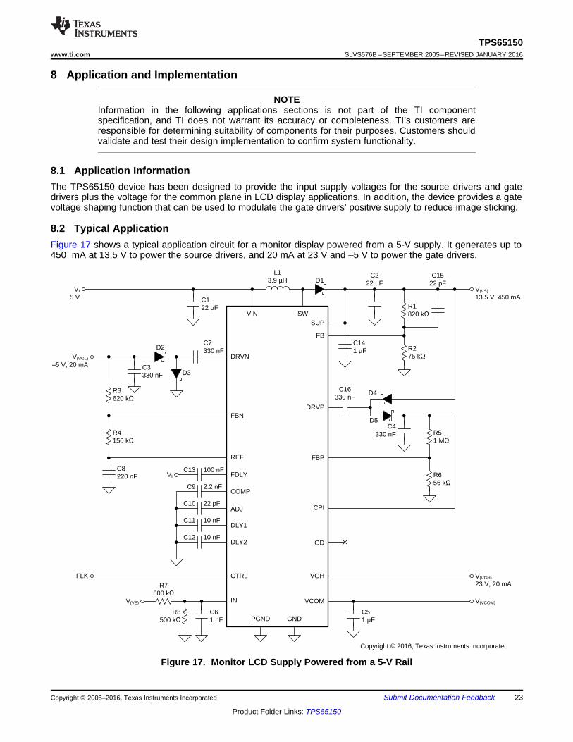
8.2 Typical ApplicationFigure 17 shows a typical application circuit for a monitor display powered from a 5-V supply. It generates up to450 mA at 13.5 V to power the source drivers, and 20 mA at 23 V and –5 V to power the gate drivers.
Figure 17. Monitor LCD Supply Powered from a 5-V Rail

24
TPS65150SLVS576B –SEPTEMBER 2005–REVISED JANUARY 2016 www.ti.com
Product Folder Links: TPS65150
Submit Documentation Feedback Copyright © 2005–2016, Texas Instruments Incorporated
Typical Application (continued)8.2.1 Design RequirementsTable 2 shows the design parameters for this example.
Table 2. Design RequirementsPARAMETER SYMBOL VALUE
Input supply voltage VI 5 VBoost converter output voltage and current V(VS) 13.5 V at 450 mABoost converter peak-to-peak output voltage ripple V(VS)(PP) 10 mVPositive charge pump output voltage and current V(CPI) 23 V at 20 mAPositive charge pump peak-to-peak output voltage ripple V(VGH)(PP) 100 mVNegative charge pump output voltage and current V(VGL) –5 V at 20 mANegative charge pump peak-to-peak output voltage ripple V(VGL)(PP) 100 mVNegative charge pump start-up delay time td1 1 msPositive charge pump start-up delay time td2 1 msFault delay time td(fault) 45 msGate voltage shaping slope 10 V/µs
8.2.2 Detailed Design Procedure
8.2.2.1 Boost Converter Design Procedure
8.2.2.1.1 Inductor Selection
Several inductors work with the TPS65150, and with external compensation the performance can be adjusted tothe specific application requirements.
The main parameter for the inductor selection is the inductor saturation current, which should be higher than thepeak switch current as calculated in Equation 2 with additional margin to cover for heavy load transients. Thealternative, more conservative approach, is to choose the inductor with a saturation current at least as high asthe maximum switch current limit of 3.4 A.
The second important parameter is the inductor DC resistance. Usually, the lower the DC resistance the higherthe efficiency. It is important to note that the inductor DC resistance is not the only parameter determining theefficiency. For a boost converter, where the inductor is the energy storage element, the type and material of theinductor influences the efficiency as well. Especially at a switching frequency of 1.2 MHz, inductor core losses,proximity effects, and skin effects become more important. Usually, an inductor with a larger form factor giveshigher efficiency. The efficiency difference between different inductors can vary from 2% to 10%. For theTPS65150, inductor values from 3.3 µH and 6.8 µH are a good choice, but other values can be used as well.Possible inductors are shown in Table 3. Equivalent parts can also be used.
Table 3. Inductor SelectionINDUCTANCE ISAT DCR MANUFACTURER PART NUMBER DIMENSIONS
4.7 µH 2.6 A 54 mΩ Coilcraft DO1813P-472HC 8.89 mm × 6.1 mm × 5 mm4.2 µH 2.2 A 23 mΩ Sumida CDRH5D28 4R2 5.7 mm × 5.7 mm × 3 mm4.7 µH 1.6 A 48 mΩ Sumida CDC5D23 4R7 6 mm × 6 mm × 2.5 mm4.2 µH 1.8 A 60 mΩ Sumida CDRH6D12 4R2 6.5 mm × 6.5 mm × 1.5 mm3.9 µH 2.6A 20 mΩ Sumida CDRH6D28 3R9 7 mm × 7 mm × 3 mm3.3 µH 1.9 A 50 mΩ Sumida CDRH6D12 4R2 6.5 mm × 6.5 mm × 1.5 mm

R1R2
= 13.5 V1.146 V
± 1 = 10.78
PD = IOVF = :0.45 A;:0.5 V; = 0.225 W
I(SW)M = :0.69;:5 V;
2:1.2 MHz;:H; + :0.45 A;
1 ± 0.69 = 1.8 A
D = 1 ± :0.85;:5 V;
13.5 V = 0.69
25
TPS65150www.ti.com SLVS576B –SEPTEMBER 2005–REVISED JANUARY 2016
Product Folder Links: TPS65150
Submit Documentation FeedbackCopyright © 2005–2016, Texas Instruments Incorporated
The first step in the design procedure is to verify whether the maximum possible output current of the boostconverter supports the specific application requirements. A simple approach is to estimate the converterefficiency, by taking the efficiency numbers from the provided efficiency curves, or use a worst case assumptionfor the expected efficiency, for example, 75%.
From Figure 19, it can be seen that the boost converter efficiency is about 85% when operating under the targetapplication conditions. Inserting these values into Equation 1 yields
WHITESPACE
(15)
WHITESPACE
and from Equation 2, the peak switch current can be calculated as
WHITESPACE
(16)
WHITESPACE
The peak switch current is the peak current that the integrated switch, inductor, and rectifier diode must be ableto handle. The calculation must be done for the minimum input voltage where the peak switch current is highest.For the calculation of the maximum current delivered by the boost converter, it must be considered that thepositive and negative charge pumps as well as the VCOM buffer run from the output of the boost converter aswell.
8.2.2.2 Rectifier Diode SelectionThe rectifier diode reverse voltage rating should be higher than the maximum output voltage of the converter(13.5 V in this application); its average forward current rating should be higher than the maximum boostconverter output current of 450 mA, and its repetitive peak forward current should be greater than or equal to thepeak switch current of 1.8 A. Not all diode manufacturers specify repetitive peak forward current; however, adiode with an average forward current rating of 1 A or higher is suitable for most practical applications.
From Equation 5, the power dissipated in the rectifier diode is given by
WHITESPACE(17)
WHITESPACE
Table 4 lists a number of suitable rectifier diodes, any of which would be suitable for this application. Equivalentparts can also be used.
Table 4. Rectifier Diode SelectionIF(AV) VR VF MANUFACTURER PART NUMBER2 A 20 V 0.44 V at 2 A Vishay Semiconductor SL222 A 20 V 0.5 V at 2 A Fairchild Semiconductor SS221 A 30 V 0.44 V at 2 A Fairchild Semiconductor MBRS130L1 A 20 V 0.45 V at 1 A Microsemi UPS1201 A 20 V 0.45 V at 1 A ON Semiconductor MBRM120
8.2.2.3 Setting the Output VoltageRearranging Equation 3 and inserting the application parameters, we get
WHITESPACE
(18)
WHITESPACE

C15 = 1
:11.2 kHz;:820 k ; = 17 pF
C15 = 1
fco:R1;
CO = 1 ± 0.69
:1.2 MHz;:10 mV;m1.8 A ± 0.45 A ± l13.5 V ± 5 V
Hp l1 ± 0.69
1.2 MHzpq = 20.3 F
26
TPS65150SLVS576B –SEPTEMBER 2005–REVISED JANUARY 2016 www.ti.com
Product Folder Links: TPS65150
Submit Documentation Feedback Copyright © 2005–2016, Texas Instruments Incorporated
Standard values of R1 = 820 kΩ and R2 = 75 kΩ result in a nominal output voltage of 13.68 V and satisfy therecommendation that the value R1 be lower than 1 MΩ.
8.2.2.4 Output Capacitor SelectionFor best output voltage filtering, a low ESR output capacitor is recommended. Ceramic capacitors have a lowESR value, but tantalum capacitors can be used as well, depending on the application. A 22-µF ceramic outputcapacitor works for most applications. Higher capacitor values can be used to improve the load transientregulation. See Table 5 for the selection of the output capacitor.
Rearranging Equation 6 and inserting the application parameters, the minimum value of output capacitance isgiven by Equation 19.
WHITESPACE
(19)
WHITESPACE
The closest standard value is 22 µF. In practice, TI recommends connecting an additional 1-µF capacitor directlyto the SUP pin to ensure a clean supply to the internal circuitry that runs from this supply voltage.
8.2.2.5 Input Capacitor SelectionFor good input voltage filtering, low ESR ceramic capacitors are recommended. A 22-µF ceramic input capacitoris sufficient for most applications. For better input voltage filtering, this value can be increased. See Table 5 forinput capacitor recommendations. Equivalent parts can also be used.
Table 5. Input and Output Capacitance SelectionCAPACITANCE VOLTAGE RATING MANUFACTURER PART NUMBER SIZE
22 µF 16 V Taiyo Yuden EMK325BY226MM 120622 µF 6.3 V Taiyo Yuden JMK316BJ226 1206
8.2.2.6 CompensationFrom Table 1, it can be seen that the recommended values for C9 and R9 when VI = 5 V are 2.2 nF and 0 Ωrespectively, and that a feedforward zero at 11.2 kHz should be added.
Rearranging Equation 7, we get
WHITESPACE
(20)
WHITESPACE
Inserting fco = 11.2 kHz and R1 = 820 kΩ, we get
WHITESPACE
WHITESPACE
In this case, a standard value of 22 pF was used.
8.2.2.7 Negative Charge Pump
8.2.2.7.1 Choosing the Output Capacitance
Rearranging Equation 9 and inserting the application parameters, the minimum recommended value of C3 isgiven by

R5R6
= 23 V
1.214 V ± 1 = 17.95
C4 = :20 mA;
2:1.2 MHz;:100 mV; = 83 nF
R3 = ± F VO
V(REF)GR4 = ± l ±5 V
1.213 VpR4 = :4.122;R4
C3 = IO
2fVO:PP; =
20 mA
2:1.2 MHz;:100 mV; = 83 nF
27
TPS65150www.ti.com SLVS576B –SEPTEMBER 2005–REVISED JANUARY 2016
Product Folder Links: TPS65150
Submit Documentation FeedbackCopyright © 2005–2016, Texas Instruments Incorporated
WHITESPACE
(21)
WHITESPACE
In this application, a capacitance of 330 nF was used to allow the same value to be used for all charge pumpcapacitances.
8.2.2.7.2 Choosing the Flying Capacitance
A minimum flying capacitance of 100 nF is recommended. In this application, a capacitance of 330 nF was usedto allow the same value to be used for all charge pump capacitances.
8.2.2.7.3 Choosing the Feedback Resistors
From Equation 22, the ratio of R3 to R4 required to generate an output voltage of –5 V is given by
WHITESPACE
(22)
WHITESPACE
Values of R3 = 620 kΩ and R4 = 150 kΩ generate a nominal output voltage of –5.014 V and load the REF pinwith only 8 µA.
8.2.2.7.4 Choosing the Diodes
The average forward current in D2 and D3 is equal to the output current and therefore a maximum of 20 mA. Thepeak repetitive forward current in D2 and D3 is equal to twice the output current and therefore less than 40 mA..
The BAT54S comprises two Schottky diodes in a small SOT-23 package and easily meets the currentrequirements of this application.
8.2.2.8 Positive Charge Pump
8.2.2.8.1 Choosing the Flying Capacitance
A minimum flying capacitance of 330 nF is recommended.
8.2.2.8.2 Choosing the Output Capacitance
Rearranging Equation 10 and inserting the application parameters, we get
WHITESPACE
(23)
WHITESPACE
In this application, a nominal value of 330 nF was used to allow the same value to be used for all charge pumpcapacitances.
8.2.2.8.3 Choosing the Feedback Resistors
Rearranging Equation 8 and inserting the application parameters, we get
WHITESPACE
(24)
WHITESPACE
Standard values of 1 MΩ and 56 kΩ result in a nominal output voltage of 22.89 V.

CFDLY = 45 ms450 k
= 100 nF
C11 = C12 = :A;:2.5 ms;
1.213 V = 10.31 nF
C10 = I:ADJ;
slope = A
10 V/s = 20 pF
28
TPS65150SLVS576B –SEPTEMBER 2005–REVISED JANUARY 2016 www.ti.com
Product Folder Links: TPS65150
Submit Documentation Feedback Copyright © 2005–2016, Texas Instruments Incorporated
8.2.2.8.4 Choosing the Diodes
The average forward current in D4 and D5 is equal to the output current and therefore a maximum of 20 mA. Thepeak repetitive forward current in D4 and D5 is equal to twice the output current and therefore less than 40 mA.
8.2.2.9 Gate Voltage ShapingRearranging Equation 13 and inserting I(ADJ) = 200 µA and slope = 10 V/µs, we get
WHITESPACE
(25)
WHITESPACE
The closest standard value for C10 is 22 pF.
8.2.2.10 Power-On SequencingRearranging Equation 12 and inserting td1 = td2 = 1 ms and Vref2 = 1.213 V, we get
WHITESPACE
(26)
WHITESPACE
10 nF is the closest standard value.
8.2.2.11 Fault DelayRearranging Equation 14 and inserting td(FDLY) = 45 ms, we get
WHITESPACE
(27)
WHITESPACE
100 nF is a standard value.
8.2.2.12 Undervoltage Lockout FunctionThe TPS65150 device contains an undervoltage lockout (UVLO) function that stops the device operating if thevoltage on the VDD pin is too low.

250 ns/div
V
10 V/div(SW)
V = 5 VI
V = 13.5 V / 300 mA(VS)
V
50 mV/div(VS)
I
1 A/divL
250 ns/div
V
10 V/div(SW)
V
50 mV/div(VS)
V = 5 V
V = 13.5 V / 10 mAI
(VS)
I
1 A/divL
0
10
20
30
40
50
60
70
80
90
100
0 50m 100m 150m 200m 250m 300mOutput Current (A)
Effi
cien
cy (
%)
VI = 2.5 VVI = 3.3 VVI = 5 V
V(VS) = 15 V
G000
1.12M
1.125M
1.13M
1.135M
1.14M
1.145M
1.15M
1.155M
−40 −20 0 20 40 60 80 100 120Free−Air Temperature (°C)
Fre
quen
cy (
Hz)
VI = 1.8 VVI = 3.6 V
V(VS) = 13.5 V
G000
0
10
20
30
40
50
60
70
80
90
100
0 100m 200m 300m 400m 500m 600m 700mOutput Current (A)
Effi
cien
cy (
%)
VI = 2.5 VVI = 3.3 VVI = 5 V
V(VS) = 10 V
G000
0
10
20
30
40
50
60
70
80
90
100
0 100m 200m 300m 400m 500mOutput Current (A)
Effi
cien
cy (
%)
VI = 2.5 VVI = 3.3 VVI = 5 V
V(VS) = 13.5 V
G000
29
TPS65150www.ti.com SLVS576B –SEPTEMBER 2005–REVISED JANUARY 2016
Product Folder Links: TPS65150
Submit Documentation FeedbackCopyright © 2005–2016, Texas Instruments Incorporated
8.2.3 Application Curves
I(VGH) = 0 mA I(VGL) = 0 mA
Figure 18. Boost Converter Efficiency (V(VS) = 10 V)
I(VGH) = 0 mA I(VGL) = 0 mA
Figure 19. Boost Converter Efficiency (V(VS) = 13.5 V)
I(VGH) = 0 mA I(VGL) = 0 mA
Figure 20. Boost Converter Efficiency (V(VS) = 15 V) Figure 21. Boost Converter Switching Frequency
Figure 22. Boost Converter Operation (Nominal Load) Figure 23. Boost Converter Operation (Light Load)

CTRL
2 V/div
V
10 V/div(VGH)
2.5 µs/div
C = 68 pF
IADJ
(VGH) = No Load
10 ms/div
td(FDLY)
V
5 V/div(VS)
V
10 V/div(VGH)
V
5 V/div(VGL)
C = 10 nFFDLY
Fault(Heavy load on V )(VS)
2.5 ms/div
V
5 V/div(VS)
V
10 V/div(VGH)
V
5 V/div(VGL)
V
5 V/div(VCOM)
1 ms/div
V
5 V/div(VS)
V
10 V/div(VGH)
V
5 V/div(VGL)
V
2 V/div(VCOM)
V = 5 V
V = 13.6 V / 300 mA
C = 1 nF
I
(VS)
(IN)
IIN500 mA/div
2.5 ms/div
V
5 V/div(VS)
V
5 V/divI
V = 5 V
V = 13.5 V
I = 200 mA
I
(VS)
(VS)
100 µs/div
V
100 mV/div(VS)
V = 3.3 V
V = 10 V, C = 22 µFI
(VS) O
I
30 mA to 330 mA(VS)
30
TPS65150SLVS576B –SEPTEMBER 2005–REVISED JANUARY 2016 www.ti.com
Product Folder Links: TPS65150
Submit Documentation Feedback Copyright © 2005–2016, Texas Instruments Incorporated
Figure 24. Boost Converter Load Transient Response Figure 25. Boost Converter Soft Start
Figure 26. Power-On Sequencing Figure 27. Power-On Sequencing With External IsolationMOSFET
Figure 28. Gate Voltage Shaping Figure 29. Adjustable Fault Detection Time

20.0
20.5
21.0
21.5
22.0
22.5
23.0
23.5
24.0
24.5
25.0
0 20m 40m 60m 80m 100mOutput Current (A)
Out
put V
olta
ge (
V)
TA = –40°CTA = 25°CTA = 85°C
V(VS) = 10 VV(VGH) = 24 V
G000
−80m
−60m
−40m
−20m
0
20m
40m
60m
80m
−160m −120m −80m −40m 0 40m 80m 120m 160mOutput Current (A)
V(V
CO
M) −
V(IN
) (V
)
V(VS) = 10 VV(VCOM) = 5 V
G000
−5.02
−5.00
−4.98
−4.96
−4.94
−4.92
−4.90
−4.88
−4.86
0 20m 40m 60m 80m 100mOutput Current (A)
Out
put V
olta
ge (
V)
TA = –40°CTA = 25°CTA = 85°C
V(VS) = 10 VV(VGL) = –5 V
G000
20.0
20.5
21.0
21.5
22.0
22.5
23.0
23.5
24.0
24.5
25.0
0 20m 40m 60m 80m 100mOutput Current (A)
Out
put V
olta
ge (
V)
TA = –40°CTA = 25°CTA = 85°C
V(VS) = 15 VV(VGH) = 24 V
G000
31
TPS65150www.ti.com SLVS576B –SEPTEMBER 2005–REVISED JANUARY 2016
Product Folder Links: TPS65150
Submit Documentation FeedbackCopyright © 2005–2016, Texas Instruments Incorporated
Figure 30. Negative Charge Pump Load Regulation Figure 31. Positive Charge Pump Load Regulation (×2)
Figure 32. Positive Charge Pump Load Regulation (×3) Figure 33. VCOM Buffer Load Regulation

VIN SW
FBSUP
DRVP
FBP
CPI
VGH
VCOM
VI FDLY
COMP
ADJ
DLY1
DLY2
100 nF
470 pF
22 pF
10 nF
10 nF
DRVN
FBN
REF
C7330 nF
C3330 nF
R3620 k
R4150 k
R256 k
R1430 k
C222 µF
C141 µF
C1547 pF
C16330 nF
C17330 nF R5
1 M
R656 k
C51 µF
C122 µF
L13.9 µH
CTRL
R8500 k
R7500 k
C61 nF
IN
PGND GND
V(VGH)
23 V, 20 mA
V(VCOM)
V(VS)
10 V, 280 mAVI
2.5 V
V(VGL)
±5 V, 20 mA
V(VS)
FLK
C8220 nF
D4
D5
D3
D2
C13
C9
C10
C11
C12GD
D1
D6 D7C4
330 nFC18
330 nF
R968 k
V(SW)
V(SW)
Copyright © 2016, Texas Instruments Incorporated
32
TPS65150SLVS576B –SEPTEMBER 2005–REVISED JANUARY 2016 www.ti.com
Product Folder Links: TPS65150
Submit Documentation Feedback Copyright © 2005–2016, Texas Instruments Incorporated
8.3 System Examples
Figure 34. Notebook LCD Supply Powered from a 2.5-V Rail

VIN SW
FB
SUP
DRVP
FBP
CPI
VGH
VCOM
VI FDLY
COMP
ADJ
DLY1
DLY2
100 nF
2.2 nF
22 pF
10 nF
10 nF
DRVN
FBN
REF
C7330 nF
C3330 nF
R3620 k
R4150 k
R275 k
R1820 k
C222 µF
C141 µF
C1522 pF
C16330 nF
C4330 nF R5
1 M
R656 k
C51 µF
C122 µF
L13.9 µH
CTRL
R8500 k
R7500 k
C61 nF
IN
PGND GND
V(VGH)
23 V, 20 mA
V(VCOM)
V(VS)
13.5 V, 450 mAVI
5 V
V(VGL)
±5 V, 20 mA
V(VS)
FLK
C8220 nF
D4
D5
D3
D2
C13
C9
C10
C11
C12GD
D1
Copyright © 2016, Texas Instruments Incorporated
33
TPS65150www.ti.com SLVS576B –SEPTEMBER 2005–REVISED JANUARY 2016
Product Folder Links: TPS65150
Submit Documentation FeedbackCopyright © 2005–2016, Texas Instruments Incorporated
System Examples (continued)
Figure 35. Monitor LCD Supply Powered from a 5-V Rail

VIN SW
FBSUP
DRVP
FBP
CPI
VGH
VCOM
VI FDLY
COMP
ADJ
DLY1
DLY2
100 nF
2.2 nF
22 pF
10 nF
10 nF
DRVN
FBN
REF
C7330 nF
C3330 nF
R3620 k
R4150 k
R275 k
R1820 k
C222 µF
C141 µF
C1522 pF
C16330 nF
C4330 nF R5
1 M
R656 k
C51 µF
C122 µF
L13.9 µH
CTRL
R8500 k
R7500 k
C61 nF
IN
PGND GND
V(VGH)
23 V, 20 mA
V(VCOM)
V(VS)
13.5 V, 450 mAVI
5 V
V(VGL)
±5 V, 20 mA
V(VS)
FLK
C8220 nF
D4
D5
D3
D2
C13
C9
C10
C11
C12GD
D1
R7510 k
R8100 k
C17220 nF
C131 µF
Q1Si2343
Copyright © 2016, Texas Instruments Incorporated
34
TPS65150SLVS576B –SEPTEMBER 2005–REVISED JANUARY 2016 www.ti.com
Product Folder Links: TPS65150
Submit Documentation Feedback Copyright © 2005–2016, Texas Instruments Incorporated
System Examples (continued)
Figure 36. Typical Isolation and Short Circuit Protection Switch for V(VS) Using Q1 and Gate Drive Signal(GD)

35
TPS65150www.ti.com SLVS576B –SEPTEMBER 2005–REVISED JANUARY 2016
Product Folder Links: TPS65150
Submit Documentation FeedbackCopyright © 2005–2016, Texas Instruments Incorporated
9 Power Supply RecommendationsThe TPS65150 device is designed to operate with input supplies from 1.8 V to 6 V. Like most integrated circuits,the input supply should be stable and free of noise if the device's full performance is to be achieved. If the inputis located more than a few centimeters away from the device, additional bulk capacitance may be required. Theinput capacitance shown in the application schematics in this data sheet is sufficient for typical applications.
10 Layout
10.1 Layout GuidelinesThe PCB layout is an important step in the power supply design. An incorrect layout could cause converterinstability, load regulation problems, noise, and EMI issues. Especially with a switching DC-DC converter at highload currents, too-thin PCB traces can cause significant voltage spikes. Good grounding is also important. Ifpossible, TI recommends using a common ground plane to minimize ground shifts between analog ground(GND) and power ground (PGND). Additionally, the following PCB design layout guidelines are recommended forthe TPS65150 device:1. Boost converter output capacitor, input capacitor and Power ground (PGND) should form a star ground or
should be directly connected together on a common power ground plane.2. Place the input capacitor directly from the input pin (VIN) to ground.3. Use a bold PCB trace to connect SUP to the output Vs.4. Place a small bypass capacitor from the SUP pin to ground.5. Use short traces for the charge-pump drive pins (DRVN, DRVP) of VGH and VGL because these traces
carry switching currents.6. Place the charge pump flying capacitors as close as possible to the DRVP and DRVN pin, avoiding a high
voltage spikes at these pins.7. Place the Schottky diodes as close as possible to the device and to the flying capacitors connected to DRVP
and DRVN.8. Carefully route the charge pump traces to avoid interference with other circuits because they carry high
voltage switching currents .9. Place the output capacitor of the VCOM buffer as close as possible to the output pin (VCOM).10. The thermal pad must be soldered to the PCB for correct thermal performance.

V(VS)
V(VGL)
GND
COMP
FB
DLY1
DLY2
VIN
SW
SW
PGND
SUP
VGH
ADJ
CTRLFBP
IN
VCOM
FBN
GND
CPI
VI
DRVP
REF
FDLY
GD
GND
GND
V(VGH)
V(CPI)
V(VCOM)
Via to inner / bottom signal layer
PGND DRVN
Thermal via to copper pour on inner / bottom signal layer
36
TPS65150SLVS576B –SEPTEMBER 2005–REVISED JANUARY 2016 www.ti.com
Product Folder Links: TPS65150
Submit Documentation Feedback Copyright © 2005–2016, Texas Instruments Incorporated
10.2 Layout Example
Figure 37. PCB Layout Example

37
TPS65150www.ti.com SLVS576B –SEPTEMBER 2005–REVISED JANUARY 2016
Product Folder Links: TPS65150
Submit Documentation FeedbackCopyright © 2005–2016, Texas Instruments Incorporated
11 Device and Documentation Support
11.1 Device Support
11.1.1 Third-Party Products DisclaimerTI'S PUBLICATION OF INFORMATION REGARDING THIRD-PARTY PRODUCTS OR SERVICES DOES NOTCONSTITUTE AN ENDORSEMENT REGARDING THE SUITABILITY OF SUCH PRODUCTS OR SERVICESOR A WARRANTY, REPRESENTATION OR ENDORSEMENT OF SUCH PRODUCTS OR SERVICES, EITHERALONE OR IN COMBINATION WITH ANY TI PRODUCT OR SERVICE.
11.2 Community ResourcesThe following links connect to TI community resources. Linked contents are provided "AS IS" by the respectivecontributors. They do not constitute TI specifications and do not necessarily reflect TI's views; see TI's Terms ofUse.
TI E2E™ Online Community TI's Engineer-to-Engineer (E2E) Community. Created to foster collaborationamong engineers. At e2e.ti.com, you can ask questions, share knowledge, explore ideas and helpsolve problems with fellow engineers.
Design Support TI's Design Support Quickly find helpful E2E forums along with design support tools andcontact information for technical support.
11.3 TrademarksE2E is a trademark of Texas Instruments.All other trademarks are the property of their respective owners.
11.4 Electrostatic Discharge CautionThese devices have limited built-in ESD protection. The leads should be shorted together or the device placed in conductive foamduring storage or handling to prevent electrostatic damage to the MOS gates.
11.5 GlossarySLYZ022 — TI Glossary.
This glossary lists and explains terms, acronyms, and definitions.
12 Mechanical, Packaging, and Orderable InformationThe following pages include mechanical, packaging, and orderable information. This information is the mostcurrent data available for the designated devices. This data is subject to change without notice and revision ofthis document. For browser-based versions of this data sheet, refer to the left-hand navigation.

www.ti.com
PACKAGE OUTLINE
C
SEE TERMINALDETAIL
24X0.30.2
2.45 0.1
24X0.50.3
1 MAX
(0.2) TYP
0.050.00
20X 0.5
2X
2.5
2X 2.5
A4.13.9
B
4.13.9
0.30.2
0.50.3
VQFN - 1 mm max heightRGE0024BPLASTIC QUAD FLATPACK - NO LEAD
4219013/A 05/2017
PIN 1 INDEX AREA
0.08 C
SEATING PLANE
1
6 13
18
7 12
24 19
(OPTIONAL)PIN 1 ID
0.1 C A B
0.05
EXPOSEDTHERMAL PAD
25 SYMM
SYMM
NOTES:
1. All linear dimensions are in millimeters. Any dimensions in parenthesis are for reference only. Dimensioning and tolerancingper ASME Y14.5M.
2. This drawing is subject to change without notice.3. The package thermal pad must be soldered to the printed circuit board for thermal and mechanical performance.
SCALE 3.000
DETAILOPTIONAL TERMINAL
TYPICAL
38
TPS65150SLVS576B –SEPTEMBER 2005–REVISED JANUARY 2016 www.ti.com
Product Folder Links: TPS65150
Submit Documentation Feedback Copyright © 2005–2016, Texas Instruments Incorporated

www.ti.com
EXAMPLE BOARD LAYOUT
0.07 MINALL AROUND
0.07 MAXALL AROUND
24X (0.25)
24X (0.6)
( 0.2) TYPVIA
20X (0.5)
(3.8)
(3.8)
( 2.45)
(R0.05)TYP
(0.975) TYP
VQFN - 1 mm max heightRGE0024BPLASTIC QUAD FLATPACK - NO LEAD
4219013/A 05/2017
SYMM
1
6
7 12
13
18
1924
SYMM
LAND PATTERN EXAMPLEEXPOSED METAL SHOWN
SCALE:15X
NOTES: (continued)
4. This package is designed to be soldered to a thermal pad on the board. For more information, see Texas Instruments literaturenumber SLUA271 (www.ti.com/lit/slua271).
5. Vias are optional depending on application, refer to device data sheet. If any vias are implemented, refer to their locations shownon this view. It is recommended that vias under paste be filled, plugged or tented.
25
SOLDER MASKOPENING
METAL UNDERSOLDER MASK
SOLDER MASKDEFINED
EXPOSEDMETAL
METAL
SOLDER MASKOPENING
NON SOLDER MASK
SOLDER MASK DETAILS
DEFINED(PREFERRED)
EXPOSEDMETAL
39
TPS65150www.ti.com SLVS576B –SEPTEMBER 2005–REVISED JANUARY 2016
Product Folder Links: TPS65150
Submit Documentation FeedbackCopyright © 2005–2016, Texas Instruments Incorporated

www.ti.com
EXAMPLE STENCIL DESIGN
24X (0.6)
24X (0.25)
20X (0.5)
(3.8)
(3.8)
4X ( 1.08)
(0.64)TYP
(0.64) TYP
(R0.05) TYP
VQFN - 1 mm max heightRGE0024BPLASTIC QUAD FLATPACK - NO LEAD
4219013/A 05/2017
NOTES: (continued)
6. Laser cutting apertures with trapezoidal walls and rounded corners may offer better paste release. IPC-7525 may have alternatedesign recommendations.
25
SYMM
METALTYP
BASED ON 0.125 mm THICK STENCILSOLDER PASTE EXAMPLE
EXPOSED PAD 2578% PRINTED SOLDER COVERAGE BY AREA UNDER PACKAGE
SCALE:20X
SYMM
1
6
7 12
13
18
1924
40
TPS65150SLVS576B –SEPTEMBER 2005–REVISED JANUARY 2016 www.ti.com
Product Folder Links: TPS65150
Submit Documentation Feedback Copyright © 2005–2016, Texas Instruments Incorporated

PACKAGE OPTION ADDENDUM
www.ti.com 13-Aug-2021
Addendum-Page 1
PACKAGING INFORMATION
Orderable Device Status(1)
Package Type PackageDrawing
Pins PackageQty
Eco Plan(2)
Lead finish/Ball material
(6)
MSL Peak Temp(3)
Op Temp (°C) Device Marking(4/5)
Samples
TPS65150PWP ACTIVE HTSSOP PWP 24 60 RoHS & Green NIPDAU Level-2-260C-1 YEAR -40 to 85 TPS65150
TPS65150PWPG4 ACTIVE HTSSOP PWP 24 60 RoHS & Green NIPDAU Level-2-260C-1 YEAR -40 to 85 TPS65150
TPS65150PWPR ACTIVE HTSSOP PWP 24 2000 RoHS & Green NIPDAU Level-2-260C-1 YEAR -40 to 85 TPS65150
TPS65150PWPRG4 ACTIVE HTSSOP PWP 24 2000 RoHS & Green NIPDAU Level-2-260C-1 YEAR -40 to 85 TPS65150
TPS65150RGER ACTIVE VQFN RGE 24 3000 RoHS & Green NIPDAU Level-2-260C-1 YEAR -40 to 85 TPS65150
TPS65150RGERG4 ACTIVE VQFN RGE 24 3000 RoHS & Green NIPDAU Level-2-260C-1 YEAR -40 to 85 TPS65150
(1) The marketing status values are defined as follows:ACTIVE: Product device recommended for new designs.LIFEBUY: TI has announced that the device will be discontinued, and a lifetime-buy period is in effect.NRND: Not recommended for new designs. Device is in production to support existing customers, but TI does not recommend using this part in a new design.PREVIEW: Device has been announced but is not in production. Samples may or may not be available.OBSOLETE: TI has discontinued the production of the device.
(2) RoHS: TI defines "RoHS" to mean semiconductor products that are compliant with the current EU RoHS requirements for all 10 RoHS substances, including the requirement that RoHS substancedo not exceed 0.1% by weight in homogeneous materials. Where designed to be soldered at high temperatures, "RoHS" products are suitable for use in specified lead-free processes. TI mayreference these types of products as "Pb-Free".RoHS Exempt: TI defines "RoHS Exempt" to mean products that contain lead but are compliant with EU RoHS pursuant to a specific EU RoHS exemption.Green: TI defines "Green" to mean the content of Chlorine (Cl) and Bromine (Br) based flame retardants meet JS709B low halogen requirements of <=1000ppm threshold. Antimony trioxide basedflame retardants must also meet the <=1000ppm threshold requirement.
(3) MSL, Peak Temp. - The Moisture Sensitivity Level rating according to the JEDEC industry standard classifications, and peak solder temperature.
(4) There may be additional marking, which relates to the logo, the lot trace code information, or the environmental category on the device.
(5) Multiple Device Markings will be inside parentheses. Only one Device Marking contained in parentheses and separated by a "~" will appear on a device. If a line is indented then it is a continuationof the previous line and the two combined represent the entire Device Marking for that device.
(6) Lead finish/Ball material - Orderable Devices may have multiple material finish options. Finish options are separated by a vertical ruled line. Lead finish/Ball material values may wrap to twolines if the finish value exceeds the maximum column width.

PACKAGE OPTION ADDENDUM
www.ti.com 13-Aug-2021
Addendum-Page 2
Important Information and Disclaimer:The information provided on this page represents TI's knowledge and belief as of the date that it is provided. TI bases its knowledge and belief on informationprovided by third parties, and makes no representation or warranty as to the accuracy of such information. Efforts are underway to better integrate information from third parties. TI has taken andcontinues to take reasonable steps to provide representative and accurate information but may not have conducted destructive testing or chemical analysis on incoming materials and chemicals.TI and TI suppliers consider certain information to be proprietary, and thus CAS numbers and other limited information may not be available for release.
In no event shall TI's liability arising out of such information exceed the total purchase price of the TI part(s) at issue in this document sold by TI to Customer on an annual basis.
OTHER QUALIFIED VERSIONS OF TPS65150 :
• Automotive : TPS65150-Q1
NOTE: Qualified Version Definitions:
• Automotive - Q100 devices qualified for high-reliability automotive applications targeting zero defects

TAPE AND REEL INFORMATION
*All dimensions are nominal
Device PackageType
PackageDrawing
Pins SPQ ReelDiameter
(mm)
ReelWidth
W1 (mm)
A0(mm)
B0(mm)
K0(mm)
P1(mm)
W(mm)
Pin1Quadrant
TPS65150PWPR HTSSOP PWP 24 2000 330.0 16.4 6.95 8.3 1.6 8.0 16.0 Q1
TPS65150RGER VQFN RGE 24 3000 330.0 12.4 4.35 4.35 1.1 8.0 12.0 Q2
PACKAGE MATERIALS INFORMATION
www.ti.com 5-Jan-2022
Pack Materials-Page 1

*All dimensions are nominal
Device Package Type Package Drawing Pins SPQ Length (mm) Width (mm) Height (mm)
TPS65150PWPR HTSSOP PWP 24 2000 350.0 350.0 43.0
TPS65150RGER VQFN RGE 24 3000 338.0 355.0 50.0
PACKAGE MATERIALS INFORMATION
www.ti.com 5-Jan-2022
Pack Materials-Page 2

TUBE
*All dimensions are nominal
Device Package Name Package Type Pins SPQ L (mm) W (mm) T (µm) B (mm)
TPS65150PWP PWP HTSSOP 24 60 530 10.2 3600 3.5
TPS65150PWPG4 PWP HTSSOP 24 60 530 10.2 3600 3.5
PACKAGE MATERIALS INFORMATION
www.ti.com 5-Jan-2022
Pack Materials-Page 3

IMPORTANT NOTICE AND DISCLAIMERTI PROVIDES TECHNICAL AND RELIABILITY DATA (INCLUDING DATA SHEETS), DESIGN RESOURCES (INCLUDING REFERENCE DESIGNS), APPLICATION OR OTHER DESIGN ADVICE, WEB TOOLS, SAFETY INFORMATION, AND OTHER RESOURCES “AS IS” AND WITH ALL FAULTS, AND DISCLAIMS ALL WARRANTIES, EXPRESS AND IMPLIED, INCLUDING WITHOUT LIMITATION ANY IMPLIED WARRANTIES OF MERCHANTABILITY, FITNESS FOR A PARTICULAR PURPOSE OR NON-INFRINGEMENT OF THIRD PARTY INTELLECTUAL PROPERTY RIGHTS.These resources are intended for skilled developers designing with TI products. You are solely responsible for (1) selecting the appropriate TI products for your application, (2) designing, validating and testing your application, and (3) ensuring your application meets applicable standards, and any other safety, security, regulatory or other requirements.These resources are subject to change without notice. TI grants you permission to use these resources only for development of an application that uses the TI products described in the resource. Other reproduction and display of these resources is prohibited. No license is granted to any other TI intellectual property right or to any third party intellectual property right. TI disclaims responsibility for, and you will fully indemnify TI and its representatives against, any claims, damages, costs, losses, and liabilities arising out of your use of these resources.TI’s products are provided subject to TI’s Terms of Sale or other applicable terms available either on ti.com or provided in conjunction with such TI products. TI’s provision of these resources does not expand or otherwise alter TI’s applicable warranties or warranty disclaimers for TI products.TI objects to and rejects any additional or different terms you may have proposed. IMPORTANT NOTICE
Mailing Address: Texas Instruments, Post Office Box 655303, Dallas, Texas 75265Copyright © 2022, Texas Instruments Incorporated