AN1428, LCD Biasing and Contrast Control...
22
2012 Microchip Technology Inc. DS01428A-page 1 AN1428 INTRODUCTION This Application Note provides methods that can be used to provide biasing voltages for Liquid Crystal displays. This document covers most of the biasing methods used in the PIC ® microcontrollers with an LCD controller. LCD TYPES LCD types and LCD waveforms determine the type of biasing that is required. There are different kinds of LCD biasing, based on the construction. There are two electrodes where the LCD waveforms are driven; they are called SEGMENTs (SEGs) and COMMONs (COMs). The LCD requires an AC waveform to be applied between these electrodes. Based on the number of SEGMENT and COMMON electrodes, the LCDs can be classified in two basic types: 1. Static or Direct Drive 2. Multiplex Displays Static or Direct Drive LCD The static waveform will have only one COMMON elec- trode and multiple SEGMENT electrodes. The number of pixels it can drive is the number of SEGMENTs on the LCD. Figure 1 shows a static LCD configuration. There are 1 COMMON and 8 SEGMENTs, so the number of pixels that can be driven is the number of COMs, multiplied by the number of SEG pins, resulting in 8 pixels. FIGURE 1: COMMON AND SEGMENT CONNECTIONS FOR STATIC DISPLAY An AC voltage needs to be applied to the SEGMENT and COMMON. For a static display, there are only two levels for the voltage that are applied. These levels, which are driving the LCD, are called bias voltages. A static LCD wave will look like a square wave. In Figure 1, SEG0 is on and SEG1 is off, and both are connected to COM0. The waveform in Figure 2 shows COM0, SEG0 and SEG1. It also shows the effective voltage between the SEG1 and SEG0, in respect to the COMMON. Author: Naveen Raj Microchip Technology Inc. COM0 SEG0 SEG1 SEG2 SEG3 SEG4 SEG5 SEG6 SEG7 COMMON SEGMENT Connection Connection LCD Biasing and Contrast Control Methods
Transcript of AN1428, LCD Biasing and Contrast Control...
AN1428LCD Biasing and Contrast Control Methods
INTRODUCTION
This Application Note provides methods that can beused to provide biasing voltages for Liquid Crystaldisplays. This document covers most of the biasingmethods used in the PIC® microcontrollers with an LCDcontroller.
LCD TYPES
LCD types and LCD waveforms determine the type ofbiasing that is required. There are different kinds ofLCD biasing, based on the construction.
There are two electrodes where the LCD waveforms aredriven; they are called SEGMENTs (SEGs) andCOMMONs (COMs). The LCD requires an AC waveformto be applied between these electrodes.
Based on the number of SEGMENT and COMMONelectrodes, the LCDs can be classified in two basictypes:
1. Static or Direct Drive
2. Multiplex Displays
Static or Direct Drive LCD
The static waveform will have only one COMMON elec-trode and multiple SEGMENT electrodes. The numberof pixels it can drive is the number of SEGMENTs onthe LCD.
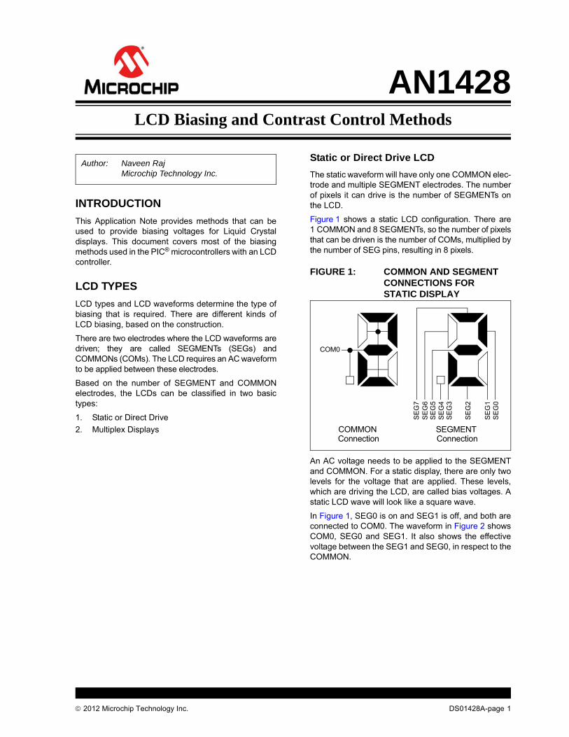
Figure 1 shows a static LCD configuration. There are1 COMMON and 8 SEGMENTs, so the number of pixelsthat can be driven is the number of COMs, multiplied bythe number of SEG pins, resulting in 8 pixels.
FIGURE 1: COMMON AND SEGMENT CONNECTIONS FOR STATIC DISPLAY
An AC voltage needs to be applied to the SEGMENTand COMMON. For a static display, there are only twolevels for the voltage that are applied. These levels,which are driving the LCD, are called bias voltages. Astatic LCD wave will look like a square wave.
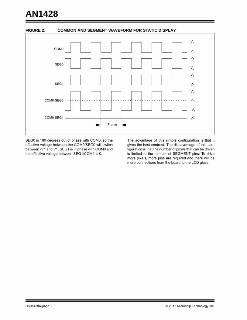
In Figure 1, SEG0 is on and SEG1 is off, and both areconnected to COM0. The waveform in Figure 2 showsCOM0, SEG0 and SEG1. It also shows the effectivevoltage between the SEG1 and SEG0, in respect to theCOMMON.
Author: Naveen RajMicrochip Technology Inc.
COM0
SE
G0
SE
G1
SE
G2
SE
G3
SE
G4
SE
G5
SE
G6
SE
G7
COMMON SEGMENT ConnectionConnection
2012 Microchip Technology Inc. DS01428A-page 1
AN1428
FIGURE 2: COMMON AND SEGMENT WAVEFORM FOR STATIC DISPLAY
SEG0 is 180 degrees out of phase with COM0, so theeffective voltage between the COM0/SEG0 will switchbetween -V1 and V1. SEG1 is in phase with COM0 andthe effective voltage between SEG1/COM1 is 0.
The advantage of this simple configuration is that itgives the best contrast. The disadvantage of this con-figuration is that the number of pixels that can be drivenis limited to the number of SEGMENT pins. To drivemore pixels, more pins are required and there will bemore connections from the board to the LCD glass.
COM0
SEG0
SEG1
COM0-SEG0
COM0-SEG1
V1
V0
V1
V0
V1
V0
V1
-V1
V0
V0
1 Frame
DS01428A-page 2 2012 Microchip Technology Inc.

AN1428
Multiplex Display
In the multiplex display, there will be more than oneCOMMON electrode, with multiple SEGMENTelectrodes. Depending on the number ofCOMMON electrodes, the glass can be defined as1/2 MUX, 1/3 MUX, 1/4 MUX, 1/8 MUX, etc.
Most of the Microchip LCD microcontrollers supportboth Static as well as Multiplex modes, up to 1/4 MUX.The newer devices, such as the PIC24FJ128GA310family devices, support up to 1/8 MUX. In a multiplexdisplay, the number of pixels that can be driven is cal-culated by multiplying the number of COMs, multipliedby the number of SEGs. For example, in thePIC24FJ128GA310 device, there are 8 COMMONsand 60 SEGMENTs. Therefore, the number of pixelsthat can be driven is 60 x 8 = 480 pixels.
The LCD multiplexing possibilities of PIC MCUs, withthe driver module configurable into 7 multiplex types,are as follows:
• 1/2 Multiplex (COM0 and COM1 are used)
• 1/3 Multiplex (COM0, COM1 and COM2 are used)
• 1/4 Multiplex (COM0, COM1, COM2 and COM3 are used)
• 1/5 Multiplex (COM0, COM1, COM2, COM3 and COM4 are used)
• 1/6 Multiplex (COM0, COM1, COM2, COM3, COM4 and COM5 are used)
• 1/7 Multiplex (COM0, COM1, COM2, COM3, COM4, COM5 and COM6 are used)
• 1/8 Multiplex (COM0, COM1, COM2, COM3, COM4, COM5, COM6 and COM7 are used)
FIGURE 3: MULTIPLEXED LCD DISPLAY
COM3
COM2
COM1
COM0
SE
G0
SE
G1
COM3
COM2
COM0
COM1
SE
G0
COM4
1/4 MUX, 1/3 Bias
1/8 MUX, 1/3 Bias
2012 Microchip Technology Inc. DS01428A-page 3
AN1428
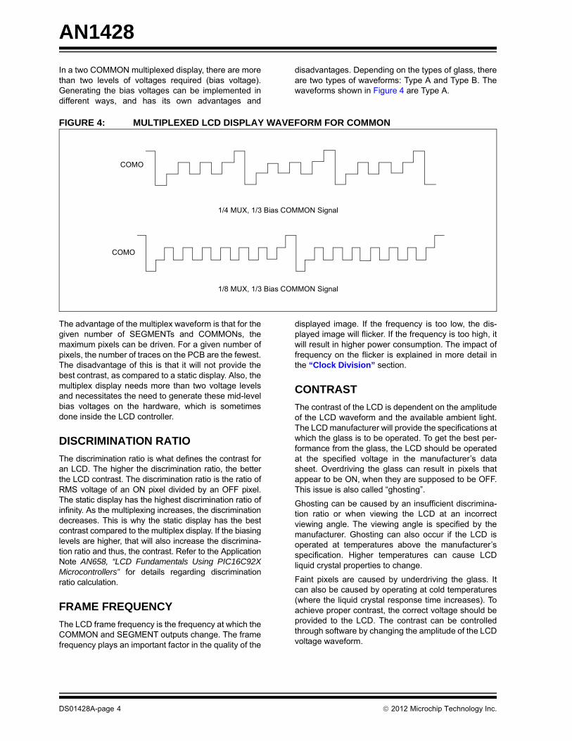
In a two COMMON multiplexed display, there are morethan two levels of voltages required (bias voltage).Generating the bias voltages can be implemented indifferent ways, and has its own advantages and
disadvantages. Depending on the types of glass, thereare two types of waveforms: Type A and Type B. Thewaveforms shown in Figure 4 are Type A.
FIGURE 4: MULTIPLEXED LCD DISPLAY WAVEFORM FOR COMMON
The advantage of the multiplex waveform is that for thegiven number of SEGMENTs and COMMONs, themaximum pixels can be driven. For a given number ofpixels, the number of traces on the PCB are the fewest.The disadvantage of this is that it will not provide thebest contrast, as compared to a static display. Also, themultiplex display needs more than two voltage levelsand necessitates the need to generate these mid-levelbias voltages on the hardware, which is sometimesdone inside the LCD controller.
DISCRIMINATION RATIO
The discrimination ratio is what defines the contrast foran LCD. The higher the discrimination ratio, the betterthe LCD contrast. The discrimination ratio is the ratio ofRMS voltage of an ON pixel divided by an OFF pixel.The static display has the highest discrimination ratio ofinfinity. As the multiplexing increases, the discriminationdecreases. This is why the static display has the bestcontrast compared to the multiplex display. If the biasinglevels are higher, that will also increase the discrimina-tion ratio and thus, the contrast. Refer to the ApplicationNote AN658, “LCD Fundamentals Using PIC16C92XMicrocontrollers” for details regarding discriminationratio calculation.
FRAME FREQUENCY
The LCD frame frequency is the frequency at which theCOMMON and SEGMENT outputs change. The framefrequency plays an important factor in the quality of the
displayed image. If the frequency is too low, the dis-played image will flicker. If the frequency is too high, itwill result in higher power consumption. The impact offrequency on the flicker is explained in more detail inthe “Clock Division” section.
CONTRAST
The contrast of the LCD is dependent on the amplitudeof the LCD waveform and the available ambient light.The LCD manufacturer will provide the specifications atwhich the glass is to be operated. To get the best per-formance from the glass, the LCD should be operatedat the specified voltage in the manufacturer’s datasheet. Overdriving the glass can result in pixels thatappear to be ON, when they are supposed to be OFF.This issue is also called “ghosting”.
Ghosting can be caused by an insufficient discrimina-tion ratio or when viewing the LCD at an incorrectviewing angle. The viewing angle is specified by themanufacturer. Ghosting can also occur if the LCD isoperated at temperatures above the manufacturer’sspecification. Higher temperatures can cause LCDliquid crystal properties to change.
Faint pixels are caused by underdriving the glass. Itcan also be caused by operating at cold temperatures(where the liquid crystal response time increases). Toachieve proper contrast, the correct voltage should beprovided to the LCD. The contrast can be controlledthrough software by changing the amplitude of the LCDvoltage waveform.
COMO
COMO
1/4 MUX, 1/3 Bias COMMON Signal
1/8 MUX, 1/3 Bias COMMON Signal
DS01428A-page 4 2012 Microchip Technology Inc.
AN1428
BIAS LEVEL IN LCD
In the discussion of the LCD types, depending on thetype and waveform, it is necessary to provide differentvoltage levels to generate the LCD waveform.
For a static display, it requires only two levels (seeFigure 5).
FIGURE 5: STATIC WAVEFORM
For a half bias, there are more than 2 voltage levels.If there is more than 1 COMMON (multiplexed), therewill be more than two levels of voltage. Figure 6shows a 1/2 bias, 1/2 MUX waveform; V1/2 isbetween the V0 and V.
FIGURE 6: 1/2 MUX, 1/2 BIAS WAVEFORM
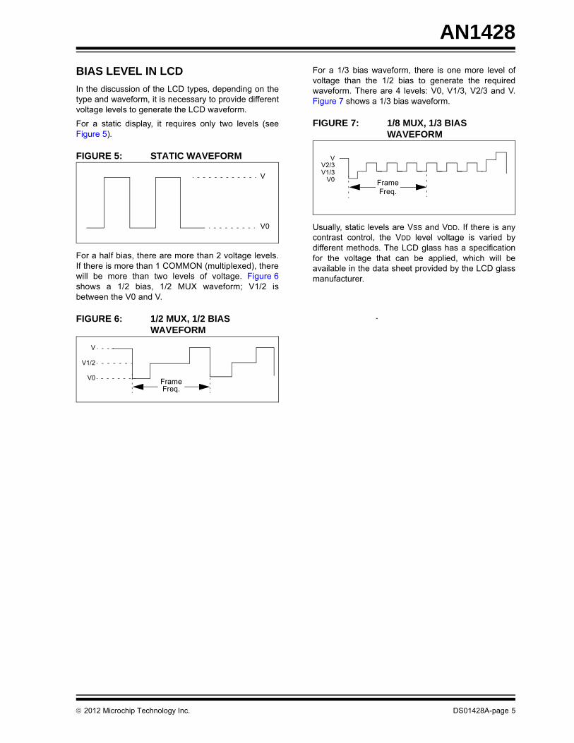
For a 1/3 bias waveform, there is one more level ofvoltage than the 1/2 bias to generate the requiredwaveform. There are 4 levels: V0, V1/3, V2/3 and V.Figure 7 shows a 1/3 bias waveform.
FIGURE 7: 1/8 MUX, 1/3 BIAS WAVEFORM
Usually, static levels are VSS and VDD. If there is anycontrast control, the VDD level voltage is varied bydifferent methods. The LCD glass has a specificationfor the voltage that can be applied, which will beavailable in the data sheet provided by the LCD glassmanufacturer.
V
V0
FrameFreq.
V
V1/2
V0
VV2/3V1/3
V0 FrameFreq.
2012 Microchip Technology Inc. DS01428A-page 5

AN1428
BIASING USING RESISTOR LADDER
External Resistor Ladder
One of the simplest ways to generate the bias voltagesis to use a resistor ladder on the board. The LCD pixelscan be considered as a capacitor, so depending on the
size of the LCD glass, capacitance can vary. Theresistor ladder bias generation provides the user theflexibility to choose the resistor, based on glass size(see Figure 8).
There is an RC charge time that must be consideredwhen the resistor and capacitor (pixel) are too high.
FIGURE 8: RESISTOR LADDER BIASING
The bias signals, VLCD0, VLCD1, VLCD2 and VLCD3,are connected to LCDBIAS0, LCDBIAS1, LCDBIAS2and LCDBIAS3, respectively. For the 1/2 bias, the mid-
point is shorted and connected to both LCDBIAS2 andLCDBIAS1. The resistor values are chosen based onthe size of the glass and the power requirements.
All the PIC18, PIC16 and PIC24 LCD microcontrollerssupport the external resistor ladder biasing.
VLCD 3VLCD 2VLCD 1VLCD 0
ToLCDDriver
Connections for External R-ladder
10 k* 10 k* 10 k*
LCD Bias 2 LCD Bias 1LCD Bias 3
* These values are provided for design guidance only and should be optimized for the application by the designer.
AVSS
Static Bias
1/2 Bias 1/3 Bias
VLCD 0 VSS VSS VSS
VLCD 1 — 1/2 VDD 1/3 VDD
VLCD 2 — 1/2 VDD 2/3 VDD
VLCD 3 VDD VDD VDD
10 k* 10 k*AVSS
VDD*
VDD*
VDD*
Static Bias
1/2 Bias
1/3 Bias
DS01428A-page 6 2012 Microchip Technology Inc.

AN1428
CONTRAST CONTROL USING EXTERNAL RESISTOR LADDER
The external resistor ladder contrast control can beachieved by adding a potentiometer on the resistorladder network. By varying the potentiometer, theamplitude of the LCD wave can be varied and the con-trast control can be achieved. In Figure 9, by changingthe potentiometer, ‘R’, the contrast can be varied. Sincethe resistor is external, the potentiometer will have tobe varied manually so that the software contrast controlcan be achieved.
FIGURE 9: CONTRAST CONTROL IN RESISTOR LADDER BIASING
Most of the newer devices from Microchip support theinternal biasing, as well as software contrast control.When the software contrast control is not implementedin the device, and if the applications where softwarecontrast control is an absolute necessity, the softwarecontrast can be achieved by using a digital pot.
With applications that require the contrast to be variedbased on temperature or ambient light, a digital pot(such as MCP40D17) can be used. The pot can beadjusted by serial communication using the PIC MCUto adjust the contrast.
FIGURE 10: SOFTWARE CONTRAST CONTROL IN RESISTOR LADDER BIASING
POWER OPTIMIZATION USING EXTERNAL RESISTOR LADDER
In the resistor ladder biasing, there is always a currentloss through the resistor ladder. If the design is powerconstrained, there should be minimal loss through theresistor ladder. One way to avoid this is to increase theresistor ladder value. This is not always the best option,since at some point, the contrast will be effected. Thisis because of the RC change time for each pixel, sinceeach pixel is a capacitor. It is important that the resistorladder is at an optimum value without affectingcontrast, but the current loss is minimal.
Figure 12 shows a COM0 waveform for an 8-COMMONLCD with 10K resistor ladder. This will provide a goodcontrast for the LCD. In battery-operated devices, wherethe total power is critical at 3V, the three 10K resistorladders cause a constant drop of 100 A. To reduce thecurrent, the resistor ladder value can be increased. Atsome point, when the resistor ladder value is increased,the contrast will become affected and the waveformshape will be altered. Therefore, an optimum resistorvalue should be chosen, based on the contrast and sizeof the pixels on the glass. Refer to Technical BriefTB1098 “Low-Power Techniques for LCD Applications”for more details on the resistor ladder selection.
LCD Glass
PIC® MCU with LCD
VDD
LCD Bias 3
LCD Bias 2
LCD Bias 1
LCD Bias 0
CO
M0
CO
M1
SE
G0
CO
M2
CO
M3
SE
G47
LCD GlassVDD
LCD Bias 3
LCD Bias 2
LCD Bias 1
LCD Bias 0
DigitalPOT
SCLSDA
PIC® MCU with LCD
CO
M0
CO
M1
CO
M2
CO
M3
SE
G0
SE
G1
SE
G47
2012 Microchip Technology Inc. DS01428A-page 7
AN1428
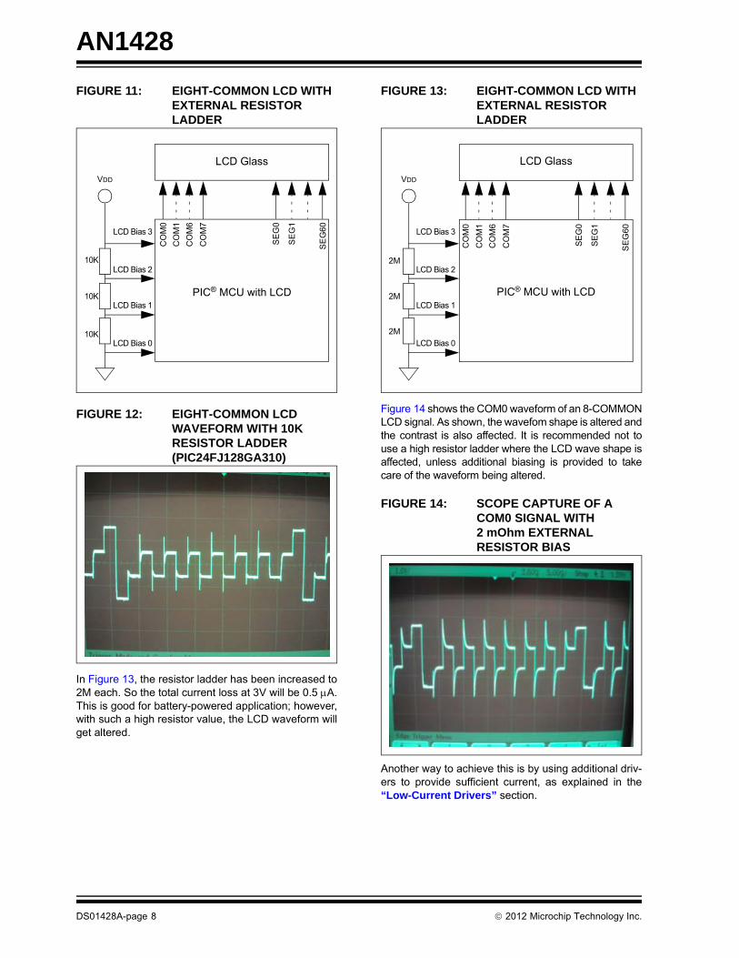
FIGURE 11: EIGHT-COMMON LCD WITH EXTERNAL RESISTOR LADDER
FIGURE 12: EIGHT-COMMON LCD WAVEFORM WITH 10K RESISTOR LADDER (PIC24FJ128GA310)
In Figure 13, the resistor ladder has been increased to2M each. So the total current loss at 3V will be 0.5 A.This is good for battery-powered application; however,with such a high resistor value, the LCD waveform willget altered.
FIGURE 13: EIGHT-COMMON LCD WITH EXTERNAL RESISTOR LADDER
Figure 14 shows the COM0 waveform of an 8-COMMONLCD signal. As shown, the wavefom shape is altered andthe contrast is also affected. It is recommended not touse a high resistor ladder where the LCD wave shape isaffected, unless additional biasing is provided to takecare of the waveform being altered.
FIGURE 14: SCOPE CAPTURE OF A COM0 SIGNAL WITH 2 mOhm EXTERNAL RESISTOR BIAS
Another way to achieve this is by using additional driv-ers to provide sufficient current, as explained in the“Low-Current Drivers” section.
VDD
LCD Bias 3
LCD Bias 2
LCD Bias 1
LCD Bias 0
10K
10K
10K
PIC® MCU with LCD
CO
M6
CO
M7
SE
G1
SE
G0
SE
G60
CO
M0
CO
M1
LCD Glass LCD Glass
PIC® MCU with LCD
VDD
LCD Bias 3
LCD Bias 2
LCD Bias 1
LCD Bias 0
2M
2M
2M
CO
M0
CO
M1
SE
G0
SE
G1
CO
M6
CO
M7
SE
G60
DS01428A-page 8 2012 Microchip Technology Inc.

AN1428
Low-Current Drivers
If the size of the glass and pixel are big, and the resistorladder is too high (in mOhm, as explained in the “Con-trast Control Using External Resistor Ladder”section), it will alter the LCD waveform. By using theMCP6042 (600 nA, Rail-to-Rail Input/Output Op Amps)between the LCD Bias 2 and LCD Bias 1, the resistorladder value can be maximized without losing anycontrast. The low quiescent current (600 nA) of theMCP6042 can be utilized in low-power, battery-operateddevices. Figure 16 shows the COM0 signal with a2 mOhm resistor ladder and a MCP6042 device. Byimplementing this method, the LCD waveform will not bealtered and the contrast will not be affected. Also, thecurrent consumption can be optimized, regardless of thesize of the LCD. Figure 16 shows the scope capture ofan 8-COMMON LCD waveform using the MCP6042buffer.
FIGURE 15: LCD WITH EXTERNAL BIASING AND BUFFER
FIGURE 16: SCOPE CAPTURE OF A COM0 SIGNAL WITH 2 mOhm EXTERNAL RESISTOR BIAS WITH BUFFER
Switch Off the Bias When Not in Use
Another way to decrease the power consumption is toswitch off the power to the resistor ladder when theLCD is not in use, or when there is no display. Providingthis option of switching the resistor ladder run time willincrease the battery life significantly. One method is touse the PIC MCU output port to drive the LCD biasresistor ladder (Figure 17). Using this method, theapplication can switch off the bias voltage any time theLCD is not used. Also, the LCD module can beswitched off, clearing LCDCON.
FIGURE 17: LCD POWER BY AN I/O PORT TO SWITCH OFF LCD
LCD Glass
PIC® MCU with LCD
VDD
LCD Bias 3
LCD Bias 2
LCD Bias 1
LCD Bias 0
2M
2M
2M MCP6042
CO
M2
CO
M3
SE
G1
SE
G0
SE
G4
7
CO
M0
CO
M1
LCD Glass
PIC® MCU with LCD
LCD Bias 3
LCD Bias 2
LCD Bias 1
LCD Bias 0
10K
10K
10K
I/O Port
CO
M2
CO
M3
SE
G1
SE
G0
SE
G47
CO
M0
CO
M1
2012 Microchip Technology Inc. DS01428A-page 9
AN1428
Power Saving Using Clock and Sleep
Power saving can be achieved by changing the clockspeed and also by putting the device to Sleep. Each ofthe methods has its own advantages and disadvantages.
Sleep Mode Operation
Putting the device in Sleep with LCD will save power,because the PIC MCU is at the lowest power mode withthe LCD enabled. Some of the devices have a low-voltage Sleep, during which the core is powered at alower voltage than regular Sleep. The LCD can operatein low-voltage Sleep with really low Sleep current.
For the LCD to function, it requires clocking. There aredifferent options for the user by which the LCD clock ischosen. The LCD can be run from:
• Main Device clock, FOSC/4 or FOSC/2 (with additional divider)
• Secondary Oscillator Clock
• LPRC or LF-INTOSC Clock
Each of these clocks can be further divided down to anominal frequency, where the LCD can operate. Thereare additional dividers where the clock can be furtherdivided through software to get the optimal frequencyfor a particular LCD.
When in Sleep, the microcontroller main clock isswitched off to save power. However, if the Secondaryor the LPRC Clock is in use, it will keep running if usedby the LCD (or other peripherals). The LCD is designedso that it can operate or shut off during Sleep. The userhas a software option to keep the LCD running duringSleep.
Putting the LCD in Sleep will save power; all of theCOMMON and SEGMENT signals will still be activeand keep the LCD on. Since the main clock is off duringSleep, the display content cannot be changed duringSleep. Therefore, during Sleep, the LCD will be on andwill display the content before the SLEEP command isexecuted.
DS01428A-page 10 2012 Microchip Technology Inc.

AN1428
Clock Division
The three clocks for the LCD have their own inbuiltdivider. This divided clock goes to the LCD module,where it can be further divided by a user-definedprescale option.
FIGURE 18: LCD CLOCK SELECTION AND PRESCALE
The LCD receives its clock after the prescale option.The user can define the frequency using the prescale.The higher the frequency, the higher the current con-sumed by the LCD module. Flicker fusion rate is a termthat can be used to define the frame rate.
Flicker fusion rate is the number of frames, per second,required to produce a continuous motion. The flickerfusion rate is dependent on the light where it is viewed.The brighter the room, the higher flicker fusion rate isrequired to eliminate the flicker. In a movie theater, theroom is darker and the flicker fusion rate is lower thana flicker fusion rate of a TV (60 Hz), which is usuallyviewed in a lighted room. For the LCD, a flicker fusionrate (frame frequency) of 30-50 Hz will produce a verygood display without any flicker.
Operating the LCD at a lower frequency has the advan-tage of low-power operation, but if the frequency is toolow because of the above explained flicker fusion rate,the display will start flickering. If too high a frequency isused, it will consume more power. So, an optimum fre-quency should be selected to optimize the contrast andpower, depending on the available light in the room.
Internal Resistor Ladder
Some of the newer PIC16/PIC18/PIC24 devices havean internal resistor ladder, implemented internally in thedevice. This unique feature of the internal resistor ladderhelps the resistor ladder to be optimized for a givenglass.
The advantage of the internal resistor ladder is:
1. Less components on the board, which reducesdesign cost.
2. Provides the user the ability to change the resis-tor ladder during run time with built-in softwarecontrast control.
3. Provides full control to switch the resistor ladderoff if the LCD is not used. This gives the user theflexibility to save power when the LCD is not used.
4. Since the bias voltages are generated internally,the external resistor ladder bias pins can beused for general purpose ports.
In the design, there are three resistor ladders. Theseresistor ladders can be changed automatically during anLCD frame in run time. The resistor ladders areclassified into high power, medium and low power. Theirtypical values are provided in Table 1. For a glass withlarger sized pixels, it will need more current to charge, sothe High-Power mode resistor ladder needs to be used.If the application needs to run an extremely small LCDwith small pixels, the low-power ladder can be used.This gives the user the flexibility to switch betweendifferent ladders, depending on the application.
FOSC/4 or FOSC/2
LPRC or LF-INTOSC
Clock Selection
Application-Defined1:16 Prescale
Prescale Selection
To LCDSecondary Oscillator
2012 Microchip Technology Inc. DS01428A-page 11

AN1428
POWER OPTIMIZATION WITH INTERNAL RESISTOR LADDER
In battery-operated devices, current consumption isextremely critical. Running the resistor ladder canconsume current. The current consumption is highestduring switching. By applying the high power duringswitching, and low power during the period where thereis no switching, the current can be further optimizedwithout losing contrast. The internal resistor ladderallows the user to keep switching between the ladders,saving power without losing contrast.
FIGURE 19: INTERNAL RESISTOR LADDER BIASING
TABLE 1: TYPICAL RESISTOR LADDER VALUES AND CURRENT AT 3V
Power ModeNominal
Resistance of Entire Ladder
IDD
Low 3 MΩ 1 µA
Medium 300 kΩ 10 µA
High 30 kΩ 100 µA
LCDBIAS3
LCDBIAS2
LCDBIAS1
VLCD3PE
VLCD2PE
VLCD1PE
LCDCST<2:0>
LCDIRELCDIRS
VDD
LRLAT<2:0>
A Power Mode
B Power Mode
LRLAP<1:0> LRLBP<1:0>
LowResistorLadder
MediumResistorLadder
HighResistorLadder
3 x VBG or VDDCORE
DS01428A-page 12 2012 Microchip Technology Inc.

AN1428
POWER MODE SELECTION
There are two power modes, designated as “Mode A”and “Mode B”. Mode A is the High-Power mode andMode B is the Low-Power mode. Mode A power isactive for a programmable time, beginning when theLCD SEGMENT waveform is transitioning.
There are 2 bits for each of these modes that decidewhich ladder is connected in that particular mode.
Mode A has 3 modes and a Disconnect mode:
Mode B has 3 modes and a Disconnect mode:
The user can use these bits to configure which ladderneeds to be connected during Mode A, and which oneneeds to be connected in Mode B. Putting the low-powerladder in both modes provides the best operation forpower, but may lose contrast because of the high-powerresistor ladder. Mode A is used during the switchingphase and should be able to source more current. It isbetter to opt for a higher current ladder for this mode anda lower current ladder for Mode B.
POWER MODE DURATION
Now, once the Mode A and Mode B resistor ladder val-ues are chosen, the user has the flexibility to decidehow long Mode A will operate, and how long Mode Bwill operate, during a SEGMENT time period.
There are three bits that can be used to select how longthese resistor ladders can be active. Software bitsselect how long Mode A is active. Mode B Power modeis active for the remaining time before the SEGMENTsor COMMONs change again. The total time for Mode Aand Mode B is, ‘T’. The three software bits that decidehow long each mode can be on during time, ‘T’:
FIGURE 20: INTERNAL RESISTOR LADDER BIAS TIMING
11 = Internal ladder is powered in High-Power mode
10 = Internal ladder is powered in Medium Power mode
01 = Internal ladder is powered in Low-Power mode
00 = Internal ladder is powered down and unconnected
11 = Internal ladder is powered in High-Power mode
10 = Internal ladder is powered in Medium Power mode
01 = Internal ladder is powered in Low-Power mode
00 = Internal ladder is powered down and unconnected
000 = Internal ladder is always in B Power mode
001 = Internal ladder is in A Power mode for 1 clock and B Power mode for 15 clocks
010 = Internal ladder is in A Power mode for 2 clocks and B Power mode for 14 clocks
011 = Internal ladder is in A Power mode for 3 clocks and B Power mode for 13 clocks
100 = Internal ladder is in A Power mode for 4 clocks and B Power mode for 12 clocks
101 = Internal ladder is in A Power mode for 5 clocks and B Power mode for 11 clocks
110 = Internal ladder is in A Power mode for 6 clocks and B Power mode for 10 clocks
111 = Internal ladder is in A Power mode for 7 clocks and B Power mode for 9 clocks
Mode A
T(1)
Mode B
SingleSEGMENT
Time
Note 1: T = Mode A Time + Mode B Time. By varying the time of Mode A and Mode B, and varying the Resistor Ladder Power modes during Mode A and Mode B, a good contrast can be achieved with the optimum power.
2012 Microchip Technology Inc. DS01428A-page 13

AN1428
Contrast Control Using Internal Resistor Bias
Each of the three resistor ladders has its own internalpotentiometer by which the resistor values can be var-ied. The resistor ladder can be varied by the contrastcontrol software bits (LCDCST<2:0>). There are sevenmodes to select where it can go from maximumcontrast to minimum contrast.
FIGURE 21: INTERNAL RESISTOR LADDER CONTRAST CONTROL REGISTER
LCDCST<2:0>: LCD Contrast Control bits
Selects the resistance of the LCD contrast controlresistor ladder:
Depending upon which ladder is being used, the corre-sponding potentiometer for that ladder will provide thecontrast control for that duration. Run-time contrastcontrol is something that is useful in applications ascontrast can vary, based on the ambient light amplitudeof the LCD waveform. By giving the value, ‘000‘, thecontrast control resistor can be taken out of the resistorladder.
Charge Pump Biasing
Some of the devices, 3V devices which are designedfor battery operated applications, have an inbuiltcharge pump to generate the bias voltages.
The advantage of the charge pump is:
• The ability for the LCD to run down to the mini-mum voltage of the device (2V, typical), as most of the 3V LCD will stop working with good contrast around 2.7V, the charge pump will keep the LCD signal to the required 3V, even if the VDD is down to 2V.
• Software contrast control is possible using the charge pump.
• With the charge pump, the LCD can get more from the given battery life.
The charge pump connection is shown in Figure 22.
FIGURE 22: CHARGE PUMP BIASING
111 = Resistor ladder is at maximum resistance (minimum contrast)
110 = Resistor ladder is at 6/7th of maximum resistance
101 = Resistor ladder is at 5/7th of maximum resistance
100 = Resistor ladder is at 4/7th of maximum resistance
011 = Resistor ladder is at 3/7th of maximum resistance
010 = Resistor ladder is at 2/7th of maximum resistance
001 = Resistor ladder is at 1/7th of maximum resistance
000 = Minimum resistance (maximum contrast); resistor ladder is shorted
Medium PowerLadder
Low-PowerLadder
High-PowerLadder
Note 1: These values are provided for design guid-ance only. They should be optimized for theapplication by the designer, based on theactual LCD specifications.
VDD
VLCAP 1
VLCAP 2
LCDBIAS3
LCDBIAS2
LCDBIAS1
LCDBIAS0
VDD
CFLY
0.047 µF(1)
C3
0.047 µF(1)
C2
0.047 µF(1)
C1
0.047 µF(1)
C0
0.047 µF(1)
DS01428A-page 14 2012 Microchip Technology Inc.

AN1428
DESIGN CONSIDERATIONS FOR THE LCD CHARGE PUMP
When designing applications that use the LCD regula-tor, with the charge pump enabled, users must alwaysconsider both the dynamic current and RMS (static)current requirements of the display, and what thecharge pump can deliver. Both dynamic and staticcurrent can be determined by Equation 1:
EQUATION 1: DYNAMIC AND STATIC CURRENT REQUIREMENTS
For dynamic current, C is the value of the capacitorsattached to LCDBIAS3 and LCDBIAS2. The variable,dV, is the voltage drop allowed on C2 and C3 during avoltage switch on the LCD display, and dT is the dura-tion of the transient current after a clock pulse occurs.For practical design purposes, these will be assumedto be 0.047 µF for C, 0.1V for dV and 1 µS for dT. Thisyields a dynamic current of 4.7 mA for 1 µS.
Users should compare the calculated current capacityagainst the requirements of the LCD. While dV and dTare relatively fixed by device design, the values of CFLY
and the capacitors on the LCDBIAS pins can bechanged to increase or decrease the current. Asalways, any changes should be evaluated in the actualcircuit for their impact on the application.
OPERATING MODES WITH CHARGE PUMP
There are four modes of operation for the LCD:
• M0: Regulator with Boost
• M1: Regulator without Boost
• M2: Resistor Ladder with Software Contrast
• M3: Resistor Ladder with Hardware Contrast
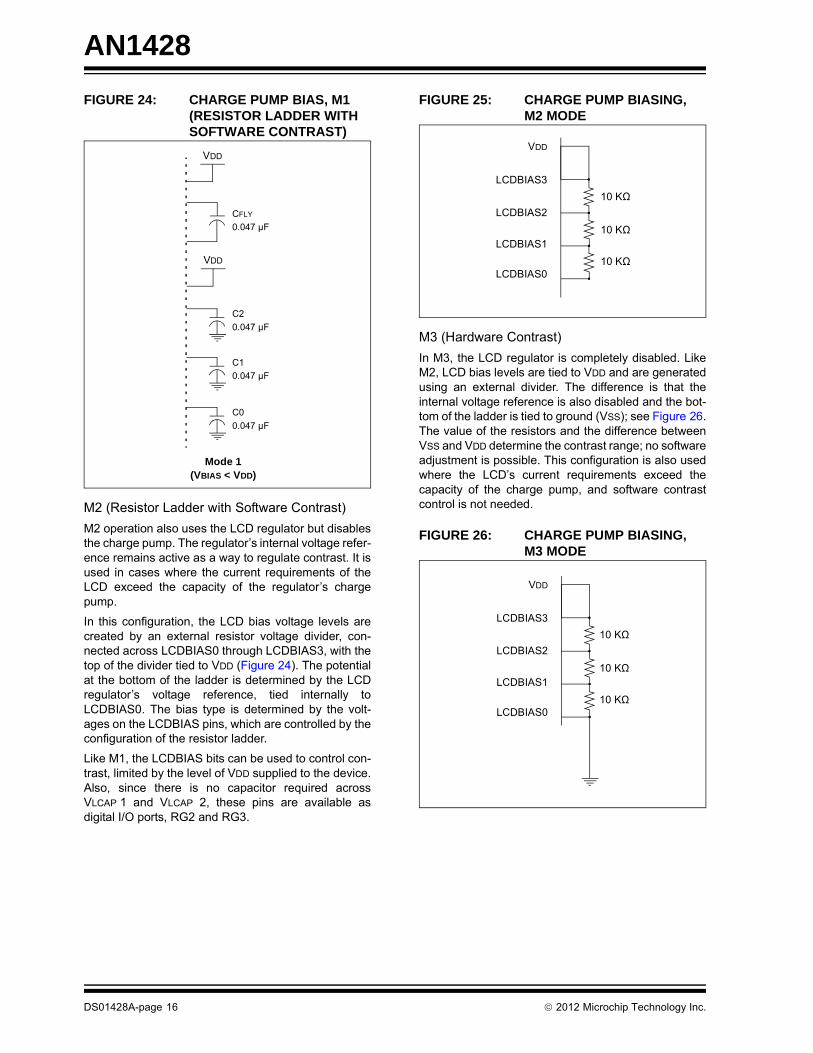
M0: Regulator with Boost
In M0 operation, the LCD charge pump feature isenabled. This allows the regulator to generate voltagesup to +3.6V to the LCD (as measured at LCDBIAS3).M0 uses a flyback capacitor, connected betweenVLCAP 1 and VLCAP 2, as well as filter capacitors onLCDBIAS0 through LCDBIAS3, to obtain the requiredvoltage boost (Figure 23).
FIGURE 23: CHARGE PUMP BIASING, M0 MODE
The output voltage (VBIAS) is the difference of potentialbetween LCDBIAS3 and LCDBIAS0. It is set by theBIAS<2:0> bits, which adjust the offset betweenLCDBIAS0 and VSS. The Flyback Capacitor (CFLY) actsas a charge storage element for large LCD loads. Thismode is useful in those cases where the voltage require-ments of the LCD are higher than the microcontroller’sVDD. It also permits software control of the display’s con-trast with the adjustment of the bias voltage, by changingthe value of the BIASx bits.
M1 (Regulator without Boost)
M1 operation is similar to M0, but does not use the LCDcharge pump. It can provide VBIAS up to the voltagelevel, supplied directly to LCDBIAS3. It can be used incases where VDD for the application is expected tonever drop below a level that can provide adequatecontrast for the LCD. The connection of external com-ponents is very similar to M0, except that LCDBIAS3must be tied directly to VDD.
The BIAS<2:0> bits can still be used to adjust contrastin software by changing VBIAS. As with M0, changingthese bits changes the offset between LCDBIAS0 andVSS. In M1, this is reflected in the change betweenLCDBIAS0 and the voltage tied to LCDBIAS3. Thus, ifVDD should change, VBIAS will also change; whereinM0, the level of VBIAS is constant (Figure 24).
I = C xdV
dT
(VBIAS up to 3.6V)
VDD
VLCAP 1
VLCAP 2
LCDBIAS3
LCDBIAS2
LCDBIAS1
LCDBIAS0
VDD
CFLY
0.047 µF
C3
0.047 µF
C2
0.047 µF
C1
0.047 µF
C0
0.047 µF
2012 Microchip Technology Inc. DS01428A-page 15
AN1428
FIGURE 24: CHARGE PUMP BIAS, M1 (RESISTOR LADDER WITH SOFTWARE CONTRAST)
M2 (Resistor Ladder with Software Contrast)
M2 operation also uses the LCD regulator but disablesthe charge pump. The regulator’s internal voltage refer-ence remains active as a way to regulate contrast. It isused in cases where the current requirements of theLCD exceed the capacity of the regulator’s chargepump.
In this configuration, the LCD bias voltage levels arecreated by an external resistor voltage divider, con-nected across LCDBIAS0 through LCDBIAS3, with thetop of the divider tied to VDD (Figure 24). The potentialat the bottom of the ladder is determined by the LCDregulator’s voltage reference, tied internally toLCDBIAS0. The bias type is determined by the volt-ages on the LCDBIAS pins, which are controlled by theconfiguration of the resistor ladder.
Like M1, the LCDBIAS bits can be used to control con-trast, limited by the level of VDD supplied to the device.Also, since there is no capacitor required acrossVLCAP 1 and VLCAP 2, these pins are available asdigital I/O ports, RG2 and RG3.
FIGURE 25: CHARGE PUMP BIASING, M2 MODE
M3 (Hardware Contrast)
In M3, the LCD regulator is completely disabled. LikeM2, LCD bias levels are tied to VDD and are generatedusing an external divider. The difference is that theinternal voltage reference is also disabled and the bot-tom of the ladder is tied to ground (VSS); see Figure 26.The value of the resistors and the difference betweenVSS and VDD determine the contrast range; no softwareadjustment is possible. This configuration is also usedwhere the LCD’s current requirements exceed thecapacity of the charge pump, and software contrastcontrol is not needed.
FIGURE 26: CHARGE PUMP BIASING, M3 MODE
Mode 1
VDD
CFLY
0.047 µF
C2
0.047 µF
VDD
C1
0.047 µF
C0
0.047 µF
(VBIAS < VDD)
VDD
LCDBIAS3
LCDBIAS2
LCDBIAS1
LCDBIAS0
10 KΩ
10 KΩ
10 KΩ
VDD
LCDBIAS3
LCDBIAS2
LCDBIAS1
LCDBIAS0
10 KΩ
10 KΩ
10 KΩ
DS01428A-page 16 2012 Microchip Technology Inc.
AN1428
Battery Power and Contrast
Most of the glass designed for 3V operation will workwell at about 2.8V-2.7V, with reasonable contrast.Below 2.7V, the LCD glass will not have enough con-trast, even though the LCD waveforms are coming out
on the LCD SEGMENT and COMMON pins. To utilizemost of the battery life, the LCD biasing can be donewith the charge pump.
As explained in “M0: Regulator with Boost”, the LCDcan operate even when the VDD is below the LCDspecification or minimum voltage.
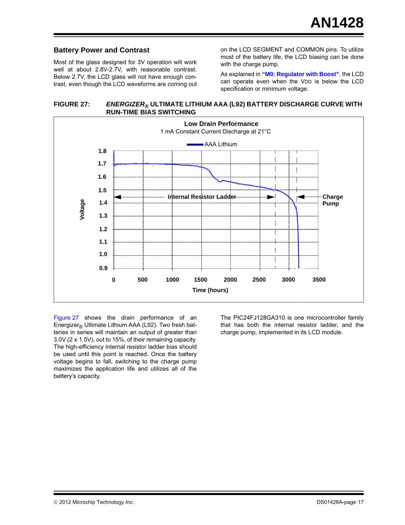
FIGURE 27: ENERGIZER® ULTIMATE LITHIUM AAA (L92) BATTERY DISCHARGE CURVE WITH RUN-TIME BIAS SWITCHING
Figure 27 shows the drain performance of anEnergizer® Ultimate Lithium AAA (L92). Two fresh bat-teries in series will maintain an output of greater than3.0V (2 x 1.5V), out to 15%, of their remaining capacity.The high-efficiency internal resistor ladder bias shouldbe used until this point is reached. Once the batteryvoltage begins to fall, switching to the charge pumpmaximizes the application life and utilizes all of thebattery’s capacity.
The PIC24FJ128GA310 is one microcontroller familythat has both the internal resistor ladder, and thecharge pump, implemented in its LCD module.
Low Drain Performance1 mA Constant Current Discharge at 21°C
AAA Lithium1.8
1.7
1.6
1.5
0.9
0 500 1000 2000 2500 3000
Time (hours)
Vo
lta
ge
1.0
1.1
1.2
1.3
1.4
1500 3500
Internal Resistor Ladder Charge Pump
2012 Microchip Technology Inc. DS01428A-page 17
AN1428
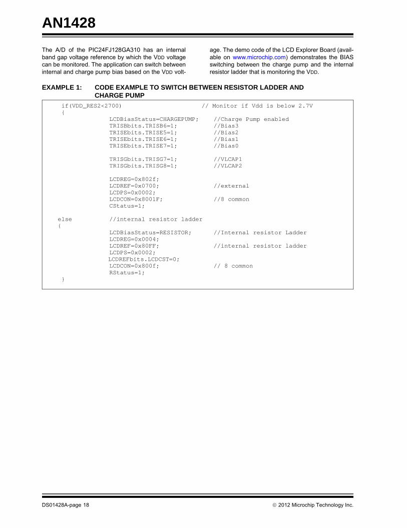
The A/D of the PIC24FJ128GA310 has an internalband gap voltage reference by which the VDD voltagecan be monitored. The application can switch betweeninternal and charge pump bias based on the VDD volt-
age. The demo code of the LCD Explorer Board (avail-able on www.microchip.com) demonstrates the BIASswitching between the charge pump and the internalresistor ladder that is monitoring the VDD.
EXAMPLE 1: CODE EXAMPLE TO SWITCH BETWEEN RESISTOR LADDER AND CHARGE PUMP
if(VDD_RES2<2700) // Monitor if Vdd is below 2.7V LCDBiasStatus=CHARGEPUMP; //Charge Pump enabled TRISBbits.TRISB6=1; //Bias3 TRISEbits.TRISE5=1; //Bias2 TRISEbits.TRISE6=1; //Bias1 TRISEbits.TRISE7=1; //Bias0
TRISGbits.TRISG7=1; //VLCAP1 TRISGbits.TRISG8=1; //VLCAP2
LCDREG=0x802f; LCDREF=0x0700; //external LCDPS=0x0002; LCDCON=0x8001F; //8 common
CStatus=1; else //internal resistor ladder
LCDBiasStatus=RESISTOR; //Internal resistor Ladder LCDREG=0x0004; LCDREF=0x80FF; //internal resistor ladder LCDPS=0x0002; LCDREFbits.LCDCST=0; LCDCON=0x800f; // 8 common RStatus=1;
DS01428A-page 18 2012 Microchip Technology Inc.

AN1428
Image Quality and Contrast
Other than the amplitude control of the waveform, thereare other factors that can affect the contrast. Thesefactors need to be considered when the LCD applicationis designed. One of the features is called viewing angle.This is usually recommended by the LCD manufacturer,so when a custom LCD is ordered, the user can defineto the vendor what kind of application it goes into.Whether it is a product which is high on the wall, such asa clock (viewed from the bottom), or something that isdesigned to be on a desk, which is viewed.
If the LCD is designed for a bottom view (or 6:00 view),it will not provide very good contrast if viewed at the top(or 12:00). However, with adjusting the contrast, someoptimization can be achieved.
In applications, there are multiple factors that need tobe considered to get the best, or the optimum contrast,and good image:
• Ambient light (or backlight if available for the LCD)
• Amplitude of the LCD waveform compared to the LCD specification
• Operating the LCD at the right temperature for which the LCD is designed
• Using the LCD with the correct viewing angle, designed by the manufacturer
• Operating the LCD with the right frame frequency (flicker fusion rate)
LCD PIC® Microcontrollers
Depending on the biasing, SEGMENTs and multiplex-ing, there are quite a few LCD PIC microcontrollersavailable, and more devices with advanced low-powerfeatures will be coming in the future. Depending on theapplication, power requirement and LCD pins, thereare quite a few different features the LCD PIC MCUcontrollers can offer.
The available products are on the following web site: http://www.microchip.com/lcd
Devices can support –
Multiplexing and Biasing:
• Static Drive
• 1/ 2 Multiplexing
• 1/ 3 Multiplexing
• 1/ 4 Multiplexing
• 1/ 5 Multiplexing
• 1/ 6 Multiplexing
• 1/ 7 Multiplexing
• 1/ 8 Multiplexing
Bias Level Support:
• Static
• 1/ 2 Bias
• 1/ 3 Bias
Bias Voltage Generation:
• External Resistor Ladder
• Internal Resistor Ladder with Software Contrast Control
• Charge Pump Bias with Software Contrast Control
LCD SEGMENTs:
• Static with a Maximum of 64 SEGMENTs can Drive 64 Pixels
• 1/8 Multiplex with 60 SEGMENTs can Drive 480 Pixels
Low-Power Operation Features:
• LCD can Operate in Sleep
• LCD can Operate in Low-Voltage/Retention Sleep
• Clock Divider for LCD to Optimize the Power
• Internal Resistor Ladder with Dynamic Power Modes
• Switching Between the Internal Resistor Ladder and Charge Pump Bias.
2012 Microchip Technology Inc. DS01428A-page 19

AN1428
REFERENCES
AN658, “LCD Fundamentals Using PIC16C92XMicrocontrollers” (DS00658)
LCD PIC® MCU Tips ‘n Tricks (DS41261)
TB084, “Contrast Control Circuits for the PIC16F91X”(DS91084)
2012 – “Energizer®”,
DS01428A-page 20 2012 Microchip Technology Inc.
Note the following details of the code protection feature on Microchip devices:
• Microchip products meet the specification contained in their particular Microchip Data Sheet.
• Microchip believes that its family of products is one of the most secure families of its kind on the market today, when used in the intended manner and under normal conditions.
• There are dishonest and possibly illegal methods used to breach the code protection feature. All of these methods, to our knowledge, require using the Microchip products in a manner outside the operating specifications contained in Microchip’s Data Sheets. Most likely, the person doing so is engaged in theft of intellectual property.
• Microchip is willing to work with the customer who is concerned about the integrity of their code.
• Neither Microchip nor any other semiconductor manufacturer can guarantee the security of their code. Code protection does not mean that we are guaranteeing the product as “unbreakable.”
Code protection is constantly evolving. We at Microchip are committed to continuously improving the code protection features of ourproducts. Attempts to break Microchip’s code protection feature may be a violation of the Digital Millennium Copyright Act. If such actsallow unauthorized access to your software or other copyrighted work, you may have a right to sue for relief under that Act.
Information contained in this publication regarding deviceapplications and the like is provided only for your convenienceand may be superseded by updates. It is your responsibility toensure that your application meets with your specifications.MICROCHIP MAKES NO REPRESENTATIONS ORWARRANTIES OF ANY KIND WHETHER EXPRESS ORIMPLIED, WRITTEN OR ORAL, STATUTORY OROTHERWISE, RELATED TO THE INFORMATION,INCLUDING BUT NOT LIMITED TO ITS CONDITION,QUALITY, PERFORMANCE, MERCHANTABILITY ORFITNESS FOR PURPOSE. Microchip disclaims all liabilityarising from this information and its use. Use of Microchipdevices in life support and/or safety applications is entirely atthe buyer’s risk, and the buyer agrees to defend, indemnify andhold harmless Microchip from any and all damages, claims,suits, or expenses resulting from such use. No licenses areconveyed, implicitly or otherwise, under any Microchipintellectual property rights.
2012 Microchip Technology Inc.
QUALITY MANAGEMENT SYSTEM CERTIFIED BY DNV
== ISO/TS 16949 ==
Trademarks
The Microchip name and logo, the Microchip logo, dsPIC, KEELOQ, KEELOQ logo, MPLAB, PIC, PICmicro, PICSTART, PIC32 logo, rfPIC and UNI/O are registered trademarks of Microchip Technology Incorporated in the U.S.A. and other countries.
FilterLab, Hampshire, HI-TECH C, Linear Active Thermistor, MXDEV, MXLAB, SEEVAL and The Embedded Control Solutions Company are registered trademarks of Microchip Technology Incorporated in the U.S.A.
Analog-for-the-Digital Age, Application Maestro, chipKIT, chipKIT logo, CodeGuard, dsPICDEM, dsPICDEM.net, dsPICworks, dsSPEAK, ECAN, ECONOMONITOR, FanSense, HI-TIDE, In-Circuit Serial Programming, ICSP, Mindi, MiWi, MPASM, MPLAB Certified logo, MPLIB, MPLINK, mTouch, Omniscient Code Generation, PICC, PICC-18, PICDEM, PICDEM.net, PICkit, PICtail, REAL ICE, rfLAB, Select Mode, Total Endurance, TSHARC, UniWinDriver, WiperLock and ZENA are trademarks of Microchip Technology Incorporated in the U.S.A. and other countries.
SQTP is a service mark of Microchip Technology Incorporated in the U.S.A.
All other trademarks mentioned herein are property of their respective companies.
© 2012, Microchip Technology Incorporated, Printed in the U.S.A., All Rights Reserved.
Printed on recycled paper.
ISBN: 978-1-62076-254-7
DS01428A-page 21
Microchip received ISO/TS-16949:2009 certification for its worldwide headquarters, design and wafer fabrication facilities in Chandler and Tempe, Arizona; Gresham, Oregon and design centers in California and India. The Company’s quality system processes and procedures are for its PIC® MCUs and dsPIC® DSCs, KEELOQ® code hopping devices, Serial EEPROMs, microperipherals, nonvolatile memory and analog products. In addition, Microchip’s quality system for the design and manufacture of development systems is ISO 9001:2000 certified.

DS01428A-page 22 2012 Microchip Technology Inc.
AMERICASCorporate Office2355 West Chandler Blvd.Chandler, AZ 85224-6199Tel: 480-792-7200 Fax: 480-792-7277Technical Support: http://www.microchip.com/supportWeb Address: www.microchip.com
AtlantaDuluth, GA Tel: 678-957-9614 Fax: 678-957-1455
BostonWestborough, MA Tel: 774-760-0087 Fax: 774-760-0088
ChicagoItasca, IL Tel: 630-285-0071 Fax: 630-285-0075
ClevelandIndependence, OH Tel: 216-447-0464 Fax: 216-447-0643
DallasAddison, TX Tel: 972-818-7423 Fax: 972-818-2924
DetroitFarmington Hills, MI Tel: 248-538-2250Fax: 248-538-2260
IndianapolisNoblesville, IN Tel: 317-773-8323Fax: 317-773-5453
Los AngelesMission Viejo, CA Tel: 949-462-9523 Fax: 949-462-9608
Santa ClaraSanta Clara, CA Tel: 408-961-6444Fax: 408-961-6445
TorontoMississauga, Ontario, CanadaTel: 905-673-0699 Fax: 905-673-6509
ASIA/PACIFICAsia Pacific OfficeSuites 3707-14, 37th FloorTower 6, The GatewayHarbour City, KowloonHong KongTel: 852-2401-1200Fax: 852-2401-3431
Australia - SydneyTel: 61-2-9868-6733Fax: 61-2-9868-6755
China - BeijingTel: 86-10-8569-7000 Fax: 86-10-8528-2104
China - ChengduTel: 86-28-8665-5511Fax: 86-28-8665-7889
China - ChongqingTel: 86-23-8980-9588Fax: 86-23-8980-9500
China - HangzhouTel: 86-571-2819-3187 Fax: 86-571-2819-3189
China - Hong Kong SARTel: 852-2401-1200 Fax: 852-2401-3431
China - NanjingTel: 86-25-8473-2460Fax: 86-25-8473-2470
China - QingdaoTel: 86-532-8502-7355Fax: 86-532-8502-7205
China - ShanghaiTel: 86-21-5407-5533 Fax: 86-21-5407-5066
China - ShenyangTel: 86-24-2334-2829Fax: 86-24-2334-2393
China - ShenzhenTel: 86-755-8203-2660 Fax: 86-755-8203-1760
China - WuhanTel: 86-27-5980-5300Fax: 86-27-5980-5118
China - XianTel: 86-29-8833-7252Fax: 86-29-8833-7256
China - XiamenTel: 86-592-2388138 Fax: 86-592-2388130
China - ZhuhaiTel: 86-756-3210040 Fax: 86-756-3210049
ASIA/PACIFICIndia - BangaloreTel: 91-80-3090-4444 Fax: 91-80-3090-4123
India - New DelhiTel: 91-11-4160-8631Fax: 91-11-4160-8632
India - PuneTel: 91-20-2566-1512Fax: 91-20-2566-1513
Japan - OsakaTel: 81-66-152-7160 Fax: 81-66-152-9310
Japan - YokohamaTel: 81-45-471- 6166 Fax: 81-45-471-6122
Korea - DaeguTel: 82-53-744-4301Fax: 82-53-744-4302
Korea - SeoulTel: 82-2-554-7200Fax: 82-2-558-5932 or 82-2-558-5934
Malaysia - Kuala LumpurTel: 60-3-6201-9857Fax: 60-3-6201-9859
Malaysia - PenangTel: 60-4-227-8870Fax: 60-4-227-4068
Philippines - ManilaTel: 63-2-634-9065Fax: 63-2-634-9069
SingaporeTel: 65-6334-8870Fax: 65-6334-8850
Taiwan - Hsin ChuTel: 886-3-5778-366Fax: 886-3-5770-955
Taiwan - KaohsiungTel: 886-7-536-4818Fax: 886-7-330-9305
Taiwan - TaipeiTel: 886-2-2500-6610 Fax: 886-2-2508-0102
Thailand - BangkokTel: 66-2-694-1351Fax: 66-2-694-1350
EUROPEAustria - WelsTel: 43-7242-2244-39Fax: 43-7242-2244-393Denmark - CopenhagenTel: 45-4450-2828 Fax: 45-4485-2829
France - ParisTel: 33-1-69-53-63-20 Fax: 33-1-69-30-90-79
Germany - MunichTel: 49-89-627-144-0 Fax: 49-89-627-144-44
Italy - Milan Tel: 39-0331-742611 Fax: 39-0331-466781
Netherlands - DrunenTel: 31-416-690399 Fax: 31-416-690340
Spain - MadridTel: 34-91-708-08-90Fax: 34-91-708-08-91
UK - WokinghamTel: 44-118-921-5869Fax: 44-118-921-5820
Worldwide Sales and Service
11/29/11