TPS3510, TPS3511: PC Power Supply Supervisors (Rev. A)
18
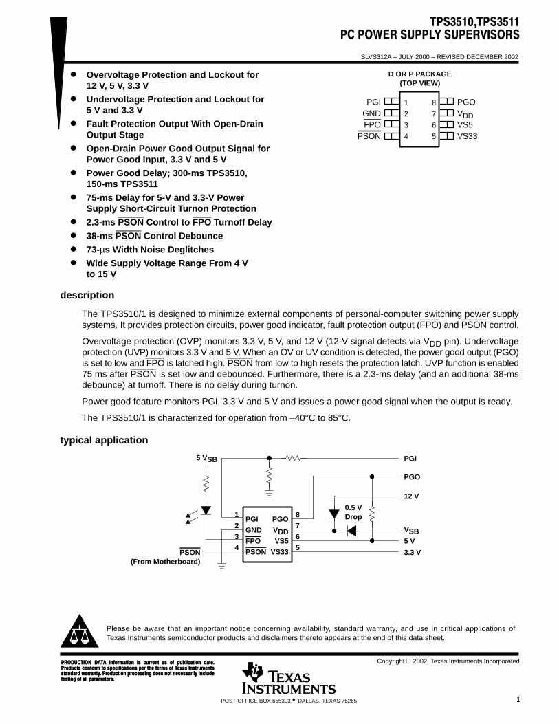
TPS3510,TPS3511 PC POWER SUPPLY SUPERVISORS SLVS312A – JULY 2000 – REVISED DECEMBER 2002 1 POST OFFICE BOX 655303 • DALLAS, TEXAS 75265 D Overvoltage Protection and Lockout for 12 V, 5 V, 3.3 V D Undervoltage Protection and Lockout for 5 V and 3.3 V D Fault Protection Output With Open-Drain Output Stage D Open-Drain Power Good Output Signal for Power Good Input, 3.3 V and 5 V D Power Good Delay; 300-ms TPS3510, 150-ms TPS3511 D 75-ms Delay for 5-V and 3.3-V Power Supply Short-Circuit Turnon Protection D 2.3-ms PSON Control to FPO Turnoff Delay D 38-ms PSON Control Debounce D 73-µs Width Noise Deglitches D Wide Supply Voltage Range From 4 V to 15 V description The TPS3510/1 is designed to minimize external components of personal-computer switching power supply systems. It provides protection circuits, power good indicator, fault protection output (FPO ) and PSON control. Overvoltage protection (OVP) monitors 3.3 V, 5 V, and 12 V (12-V signal detects via V DD pin). Undervoltage protection (UVP) monitors 3.3 V and 5 V. When an OV or UV condition is detected, the power good output (PGO) is set to low and FPO is latched high. PSON from low to high resets the protection latch. UVP function is enabled 75 ms after PSON is set low and debounced. Furthermore, there is a 2.3-ms delay (and an additional 38-ms debounce) at turnoff. There is no delay during turnon. Power good feature monitors PGI, 3.3 V and 5 V and issues a power good signal when the output is ready. The TPS3510/1 is characterized for operation from –40°C to 85°C. typical application 1 2 3 4 8 7 6 5 PGI GND FPO PSON PGO V DD VS5 VS33 PSON (From Motherboard) 5 V SB PGO 0.5 V Drop PGI 12 V V SB 5 V 3.3 V Copyright 2002, Texas Instruments Incorporated PRODUCTION DATA information is current as of publication date. Products conform to specifications per the terms of Texas Instruments standard warranty. Production processing does not necessarily include testing of all parameters. PRODUCTION DATA information is current as of publication date. Products conform to specifications per the terms of Texas Instruments standard warranty. Production processing does not necessarily include testing of all parameters. Please be aware that an important notice concerning availability, standard warranty, and use in critical applications of Texas Instruments semiconductor products and disclaimers thereto appears at the end of this data sheet. 1 2 3 4 8 7 6 5 PGI GND FPO PSON PGO V DD VS5 VS33 D OR P PACKAGE (TOP VIEW)
Transcript of TPS3510, TPS3511: PC Power Supply Supervisors (Rev. A)
���������������� ��� � ������ ��� �������
SLVS312A – JULY 2000 – REVISED DECEMBER 2002
1POST OFFICE BOX 655303 • DALLAS, TEXAS 75265
� Overvoltage Protection and Lockout for12 V, 5 V, 3.3 V
� Undervoltage Protection and Lockout for5 V and 3.3 V
� Fault Protection Output With Open-DrainOutput Stage
� Open-Drain Power Good Output Signal forPower Good Input, 3.3 V and 5 V
� Power Good Delay; 300-ms TPS3510,150-ms TPS3511
� 75-ms Delay for 5-V and 3.3-V PowerSupply Short-Circuit Turnon Protection
� 2.3-ms PSON Control to FPO Turnoff Delay
� 38-ms PSON Control Debounce
� 73-µs Width Noise Deglitches
� Wide Supply Voltage Range From 4 V to 15 V
description
The TPS3510/1 is designed to minimize external components of personal-computer switching power supplysystems. It provides protection circuits, power good indicator, fault protection output (FPO) and PSON control.
Overvoltage protection (OVP) monitors 3.3 V, 5 V, and 12 V (12-V signal detects via VDD pin). Undervoltageprotection (UVP) monitors 3.3 V and 5 V. When an OV or UV condition is detected, the power good output (PGO)is set to low and FPO is latched high. PSON from low to high resets the protection latch. UVP function is enabled75 ms after PSON is set low and debounced. Furthermore, there is a 2.3-ms delay (and an additional 38-msdebounce) at turnoff. There is no delay during turnon.
Power good feature monitors PGI, 3.3 V and 5 V and issues a power good signal when the output is ready.
The TPS3510/1 is characterized for operation from –40°C to 85°C.
typical application
1
2
3
4
8
7
6
5
PGI
GND
FPO
PSON
PGO
VDDVS5
VS33PSON(From Motherboard)
5 VSB
PGO
0.5 VDrop
PGI
12 V
VSB5 V
3.3 V
Copyright 2002, Texas Instruments Incorporated��������� ���� ����������� �� !��"�� �� �� #!$%� ����� &��"'���&! �� ������ �� �#" ��� ������ #"� �(" �"��� �� �")�� �����!�"�������&��& *������+' ���&! ���� #�� "����, &�"� ��� �" "�����%+ �� %!&"�"����, �� �%% #����"�"��'
��������� ���� ����������� �� !��"�� �� �� #!$%� ����� &��"'���&! �� ������ �� �#" ��� ������ #"� �(" �"��� �� �")�� �����!�"�������&��& *������+' ���&! ���� #�� "����, &�"� ��� �" "�����%+ �� %!&"�"����, �� �%% #����"�"��'
Please be aware that an important notice concerning availability, standard warranty, and use in critical applications ofTexas Instruments semiconductor products and disclaimers thereto appears at the end of this data sheet.
1
2
3
4
8
7
6
5
PGIGNDFPO
PSON
PGOVDDVS5VS33
D OR P PACKAGE(TOP VIEW)
���������������� ��� � ������ ��� �������
SLVS312A – JULY 2000 – REVISED DECEMBER 2002
2 POST OFFICE BOX 655303 • DALLAS, TEXAS 75265
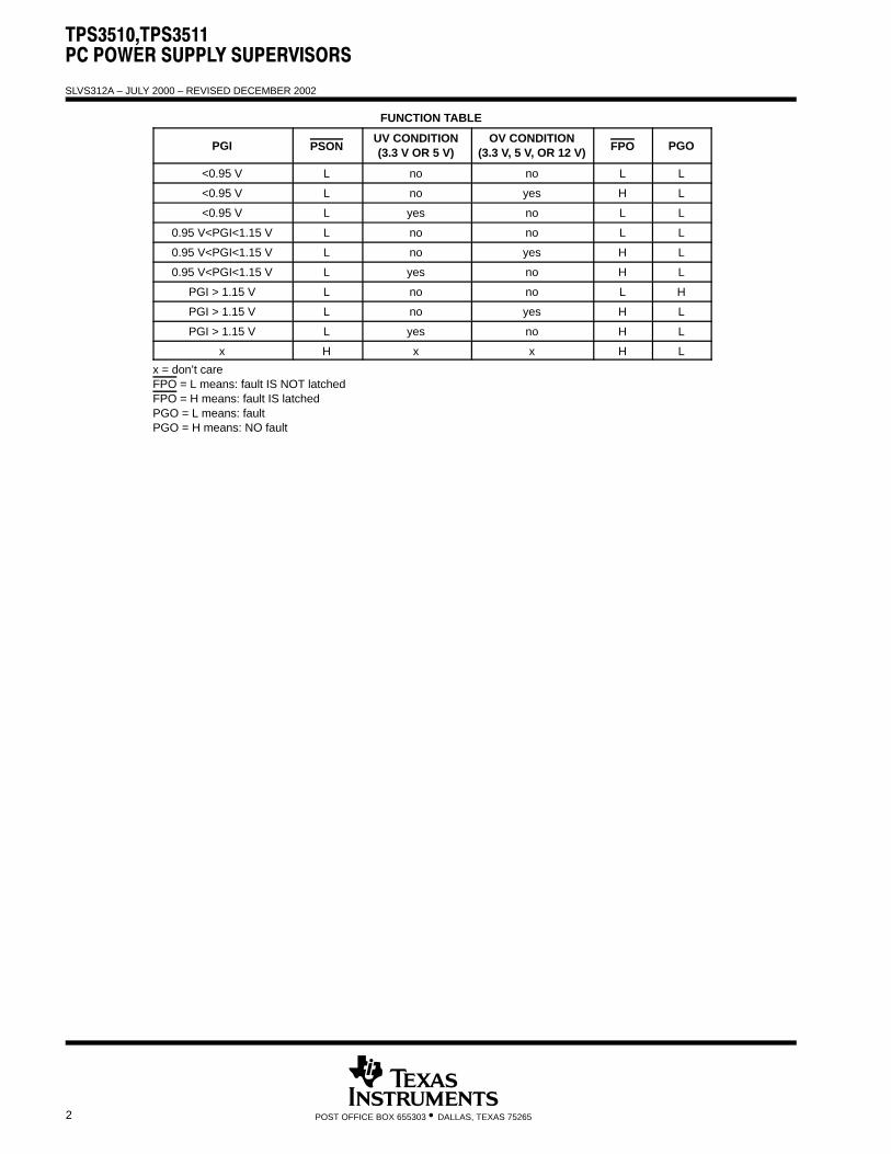
FUNCTION TABLE
PGI PSONUV CONDITION(3.3 V OR 5 V)
OV CONDITION(3.3 V, 5 V, OR 12 V) FPO PGO
<0.95 V L no no L L
<0.95 V L no yes H L
<0.95 V L yes no L L
0.95 V<PGI<1.15 V L no no L L
0.95 V<PGI<1.15 V L no yes H L
0.95 V<PGI<1.15 V L yes no H L
PGI > 1.15 V L no no L H
PGI > 1.15 V L no yes H L
PGI > 1.15 V L yes no H L
x H x x H L
x = don’t careFPO = L means: fault IS NOT latchedFPO = H means: fault IS latchedPGO = L means: faultPGO = H means: NO fault
���������������� ��� � ������ ��� �������
SLVS312A – JULY 2000 – REVISED DECEMBER 2002
3POST OFFICE BOX 655303 • DALLAS, TEXAS 75265
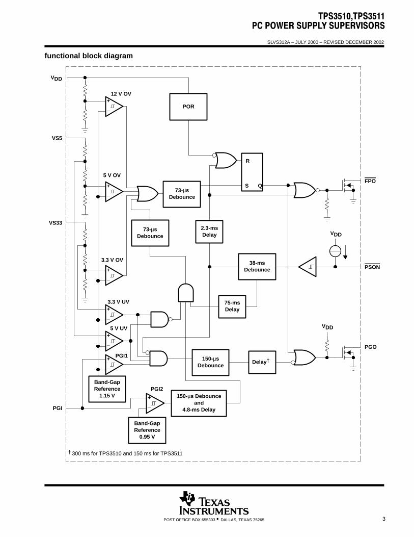
functional block diagram
_+
_+
_+
_+
_+
_+
Band-GapReference
1.15 V
_+
Band-GapReference
0.95 V
73-µsDebounce
73-µsDebounce
150-µs Debounceand
4.8-ms Delay
POR
2.3-msDelay
150-µsDebounce
R
S
75-msDelay
38-msDebounce
Delay†
VDD
VDD
VDD
VS5
VS33
PGI
FPO
PSON
PGO
12 V OV
5 V OV
3.3 V OV
Q
3.3 V UV
PGI2
PGI1
5 V UV
† 300 ms for TPS3510 and 150 ms for TPS3511

���������������� ��� � ������ ��� �������
SLVS312A – JULY 2000 – REVISED DECEMBER 2002
4 POST OFFICE BOX 655303 • DALLAS, TEXAS 75265
timing diagram
td1 tbtd1
td2
td1PG OFFDelay
ProtectOccur
PSON Off
PSONOn
AC Off
VDD
PSON
FPO
PGI
3.3 V, 5 V
12 V
PGO
PSONOn
Terminal Functions
TERMINALI/O DESCRIPTION
NAME NO.I/O DESCRIPTION
FPO 3 O Inverted fault protection output, open drain output stage
GND 2 Ground
PGI 1 I Power good input
PGO 8 O Power good output, open drain output stage
PSON 4 I ON/OFF control
VDD 7 I Supply voltage/12 V overvoltage protection input pin
VS33 5 I 3.3 V over/undervoltage protection
VS5 6 I 5 V over/undervoltage protection
���������������� ��� � ������ ��� �������
SLVS312A – JULY 2000 – REVISED DECEMBER 2002
5POST OFFICE BOX 655303 • DALLAS, TEXAS 75265
detailed description
power good and power good delay
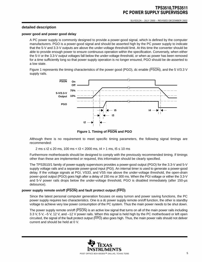
A PC power supply is commonly designed to provide a power-good signal, which is defined by the computermanufacturers. PGO is a power-good signal and should be asserted high by the PC power supply to indicatethat the 5-V and 3.3-V outputs are above the under-voltage threshold limit. At this time the converter should beable to provide enough power to ensure continuous operation within the specification. Conversely, when eitherthe 5-V or the 3.3-V output voltages fall below the under-voltage threshold, or when ac power has been removedfor a time sufficiently long so that power supply operation is no longer ensured, PGO should be de-asserted toa low state.
Figure 1 represents the timing characteristics of the power good (PGO), dc enable (PSON), and the 5 V/3.3 Vsupply rails.
t2
t3
t5 t4
5-V/3.3-VOutput
PSON
PGO
OnOff
75%
10%
Figure 1. Timing of PSON and PGO
Although there is no requirement to meet specific timing parameters, the following signal timings arerecommended:
2 ms ≤ t2 ≤ 20 ms, 100 ms < t3 < 2000 ms, t4 > 1 ms, t5 ≤ 10 ms
Furthermore motherboards should be designed to comply with the previously recommended timing. If timingsother than these are implemented or required, this information should be clearly specified.
The TPS3510/1 family of power-supply supervisors provides a power-good output (PGO) for the 3.3-V and 5-Vsupply voltage rails and a separate power-good input (PGI). An internal timer is used to generate a power-gooddelay. If the voltage signals at PGI, VS33, and VS5 rise above the under-voltage threshold, the open-drainpower-good output (PGO) goes high after a delay of 150 ms or 300 ms. When the PGI voltage or either the 3.3-Vand 5-V power rails drops below the under-voltage threshold, PGO is disabled immediately (after 150-µsdebounce).
power supply remote on/off (PSON) and fault protect output (FPO)
Since the latest personal computer generation focuses on easy turnon and power saving functions, the PCpower supply requires two characteristics. One is a dc power supply remote on/off function, the other is standbyvoltage to achieve very low power consumption of the PC system. Thus the main power needs to be shut down.
The power supply remote on/off (PSON) is an active low signal that turns on all of the main power rails including3.3 V, 5 V, –5 V, 12 V, and –12 V power rails. When this signal is held high by the PC motherboard or left opencircuited, the signal of the fault protect output (FPO) also goes high. Thus, the main power rails should not delivercurrent and should be held at 0 V.

���������������� ��� � ������ ��� �������
SLVS312A – JULY 2000 – REVISED DECEMBER 2002
6 POST OFFICE BOX 655303 • DALLAS, TEXAS 75265
power supply remote on/off (PSON) and fault protect output (FPO)(continued)
When the FPO signal is held high due to an occurring fault condition, the fault status is latched and the outputsof the main power rails should not deliver current but are held at 0 V. Toggling the power supply remote on/off(PSON) from low to high resets the fault-protection latch. During this fault condition only the standby power isnot affected.
When PSON goes from high to low or low to high, the 38-ms debounce block is active to avoid a glitch on theinput that disables/enables the FPO output. During this period the under-voltage function is disabled for 75 msto prevent turnon failure. At turnoff, there is an additional delay of 2.3 ms from PSON to FPO.
Power should be delivered to the rails only if the PSON signal is held at ground potential, thus FPO is active-low.The FPO pin can be connected to 5 V (or up to 15 V) through a pullup resistor.
undervoltage protection
The TPS3510/1 provides under-voltage protection (UVP) for the 3.3-V and 5-V rails. When an undervoltagecondition appears at either one of the 3.3-V (VS33) or 5-V (VS5) input pins for more than 146 µs, the FPO outputgoes high and PGO goes low. Also, this fault condition is latched until PSON is toggled from low to high or VDDis removed.
The need for undervoltage protection is often overlooked in off-line switching power supply system design. Butit is very important in battery-powered or hand-held equipment since the TTL or CMOS logic often results inmalfunction.
In flyback or forward-type off-line switching power supplies, usually designed for low power, the overloadprotection design is very simple. Most of these types of power supplies are only sensing the input current foran overload condition. The trigger point needs to be set much higher than the maximum load in order to preventfalse turnon.
However, this causes one critical problem. If the connected load is larger than the maximum allowable load butsmaller than the trigger point, the system always becomes overheated with failure and damage occurring.
overvoltage protection
The overvoltage protection (OVP) of TPS3510/1 monitors 3.3 V, 5 V, and 12 V (12 V is sensed via the VDD pin).When an overvoltage condition appears at one of the 3.3-V, 5-V, or 12-V input pins for more than 73 µs, the FPOoutput goes high and PGO goes low. Also, this fault condition is latched until PSON is toggled from low to highor VDD is removed. During fault conditions, most power supplies have the potential to deliver higher outputvoltages than those normally specified or required. In unprotected equipment, it is possible for output voltagesto be high enough to cause internal or external damage of the system. To protect the system under theseabnormal conditions, it is common practice to provide overvoltage protection within the power supply.
Because TTL and CMOS circuits are very vulnerable to overvoltages, it is becoming industry standard to provideovervoltage protection on all 3.3-V and 5-V outputs. However, not only the 3.3-V and 5-V rails for the logic circuitson the motherboard need to be protected, but also the 12-V peripheral devices such as the hard disk, floppydisk, and CD-ROM players etc., need to be protected.
short-circuit power supply turnon
During safety testing the power supply might have tied the output voltage direct to ground. If this happens duringthe normal operating, this is called a short-circuit or over-current condition. When it happens before the powersupply turns on, this is called a short-circuit power supply turnon. It can happen during the design period, in theproduction line, at quality control inspection or at the end user. The TPS3510/1 provides an undervoltageprotection function with a 75-ms delay after PSON is set low.
���������������� ��� � ������ ��� �������
SLVS312A – JULY 2000 – REVISED DECEMBER 2002
7POST OFFICE BOX 655303 • DALLAS, TEXAS 75265
absolute maximum ratings over operating free-air temperature (unless otherwise noted)†
Supply voltage, VDD (see Note1) 16 V. . . . . . . . . . . . . . . . . . . . . . . . . . . . . . . . . . . . . . . . . . . . . . . . . . . . . . . . . . . . . Output voltage VO: FPO 16 V. . . . . . . . . . . . . . . . . . . . . . . . . . . . . . . . . . . . . . . . . . . . . . . . . . . . . . . . . . . . . . . . . . . .
PGO 8 V. . . . . . . . . . . . . . . . . . . . . . . . . . . . . . . . . . . . . . . . . . . . . . . . . . . . . . . . . . . . . . . . . . . . . All other pins (see Note 1) –0.3 V to 16 V. . . . . . . . . . . . . . . . . . . . . . . . . . . . . . . . . . . . . . . . . . . . . . . . . . . . . . . . . . Continuous total power dissipation See Dissipation Rating Table. . . . . . . . . . . . . . . . . . . . . . . . . . . . . . . . . . . . . . Operating free-air temperature range, TA –40°C to 85°C. . . . . . . . . . . . . . . . . . . . . . . . . . . . . . . . . . . . . . . . . . . . . Storage temperature range, Tstg –65°C to 150°C. . . . . . . . . . . . . . . . . . . . . . . . . . . . . . . . . . . . . . . . . . . . . . . . . . . . Soldering temperature 260°C. . . . . . . . . . . . . . . . . . . . . . . . . . . . . . . . . . . . . . . . . . . . . . . . . . . . . . . . . . . . . . . . . . . .
† Stresses beyond those listed under “absolute maximum ratings” may cause permanent damage to the device. These are stress ratings only, andfunctional operation of the device at these or any other conditions beyond those indicated under “recommended operating conditions” is notimplied. Exposure to absolute–maximum–rated conditions for extended periods may affect device reliability.
NOTE 1: All voltage values are with respect to GND.
DISSIPATION RATING TABLE
PACKAGETA ≤ 25°C
POWER RATINGDERATING FACTORABOVE TA = 25°C
TA = 70°CPOWER RATING
TA = 85°CPOWER RATING
P 1092 mW 8.74 mW/°C 699 mW 568 mW
D 730 mW 5.84 mW/°C 467 mW 379 mW
recommended operating conditions at specified temperature range
MIN NOM MAX UNIT
Supply voltage, VDD 4 15 V
PSON, VS5, VS33 7
Input voltage, VI PGIVDD + 0.3 V(max = 7 V)
V
Output voltage VFPO 15
VOutput voltage, VO PGO 7V
O tp t sink c rrent IFPO 20
mAOutput sink current, IO,sink PGO 10mA
Supply voltage rising time, tr See Note 2 1 ms
Operating free-air temperature range, TA –40 85 °C
NOTE 2: VDD rising and falling slew rate must be less than 14 V/ms.
���������������� ��� � ������ ��� �������
SLVS312A – JULY 2000 – REVISED DECEMBER 2002
8 POST OFFICE BOX 655303 • DALLAS, TEXAS 75265
electrical characteristics over recommended operating conditions (unless otherwise noted)
overvoltage protectionPARAMETER TEST CONDITIONS MIN TYP MAX UNIT
VS33 3.7 3.9 4.1
Overvoltage threshold VS5 5.7 6.1 6.5 VOvervoltage threshold
VDD 13.2 13.8 14.4
V
ILKG Leakage current (FPO) V(FPO) = 5 V 5 µA
VOL Low-level output voltage (FPO) VDD = 5 V, Isink = 20 mA 0.7 V
Noise deglitch time OVP VDD = 5 V 35 73 110 µs
PGI and PGOPARAMETER TEST CONDITIONS MIN TYP MAX UNIT
V Inp t threshold oltage (PGI)PGI1 1.1 1.15 1.2
VVPGI Input threshold voltage (PGI)PGI2 0.9 0.95 1
V
V Under oltage thresholdVS33 2 2.2 2.4
VVIT Undervoltage thresholdVS5 3.3 3.5 3.7
V
ILKG Leakage current (PGO) PGO = 5 V 5 µA
VOL Low-level output voltage (PGO) VDD = 4 V, Isink = 10 mA 0.4 V
Short-circuit protection delay 3.3 V, 5 V 49 75 114 ms
TP3510PGI to PGO
200 300 450
td1 Delay time TP3511PGI to PGO
VDD = 5 V 100 150 225 mstd1 Delay time
PGI to FPO
VDD 5 V
3.2 4.8 7.2
ms
PGI to PGO 88 150 225
Noise deglitch time PGI to FPO VDD = 5 V 180 296 445 µsNoise deglitch time
UVP to FPO
VDD 5 V
82 146 220
µs
PSON controlPARAMETER TEST CONDITIONS MIN TYP MAX UNIT
II Input pullup current PSON = 0 V 120 µA
VIH High-level input voltage 2.4 V
VIL Low-level input voltage 1.2 V
tb Debounce time (PSON) VDD = 5 V 24 38 57 ms
td2 Delay time (PSON to FPO) VDD = 5 V tb+1.1 tb+2.3 tb+4 ms
total devicePARAMETER TEST CONDITIONS MIN TYP MAX UNIT
IDD Supply current PSON = 5 V 1 mA

���������������� ��� � ������ ��� �������
SLVS312A – JULY 2000 – REVISED DECEMBER 2002
9POST OFFICE BOX 655303 • DALLAS, TEXAS 75265
TYPICAL CHARACTERISTICS
Figure 2
400
200
–100
–3000 2.5 5 7.5 15
– S
up
ply
Cu
rren
t –
SUPPLY CURRENTvs
SUPPLY VOLTAGE
300
100
0
–200
10 12.5
I DD
Aµ
VDD – Supply Voltage – V
PGI = 1.4 VPSON = 5 V
TA = –40°C
TA = 85°C
TA = 25°C
TA = 0°C
Figure 3
–60
–100
0 1 2 3 6 7
–20
INPUT CURRENT (PSON)vs
INPUT VOLTAGE (PSON)20
0
–40
–80
–120
–140 4 5
VI – Input Voltage – V
II–
Inp
ut
Cu
rren
t –
Aµ
TA = –40°CTA = 0°CTA = 25°CTA = 85°C
VDD = 4 V
Figure 4
VDD = 4 VPSON = GND
2
1
00 20 40 60 80 120
– L
ow
-Lev
el O
utp
ut
Volt
age
– V
3
4
LOW-LEVEL OUTPUT VOLTAGE (FPO)vs
LOW-LEVEL OUTPUT CURRENT (FPO)
100IOL – Low-Level Output Current – mA
V OL
TA = –40°C
TA = 85°C
TA = 25°C
TA = 0°C
Figure 5
400
200
00 5 10 15 20
– L
ow
-Lev
el O
utp
ut
Volt
age
– m
V
600
800
LOW-LEVEL OUTPUT VOLTAGE (FPO)vs
LOW-LEVEL OUTPUT CURRENT (FPO)
25IOL – Low-Level Output Current – mA
V OL
TA = –40°C
TA = 85°C
TA = 25°C
VDD = 4 VPSON = GNDExploded View
TA = 0°C
300
100
500
700

���������������� ��� � ������ ��� �������
SLVS312A – JULY 2000 – REVISED DECEMBER 2002
10 POST OFFICE BOX 655303 • DALLAS, TEXAS 75265
TYPICAL CHARACTERISTICS
Figure 6
VDD = 4 VPSON = GND
2
1
00 25 50 75 100 150
– L
ow
-Lev
el O
utp
ut
Volt
age
– V
3
4
LOW-LEVEL OUTPUT VOLTAGE (PGO)vs
LOW-LEVEL OUTPUT CURRENT (PGO)
125IOL – Low-Level Output Current – mA
V OL
TA = –40°C
TA = 0°C
TA = 85°C
TA = 25°C
Figure 7
400
200
00 5 10 15 20
– L
ow
-Lev
el O
utp
ut
Volt
age
– m
V
600
LOW-LEVEL OUTPUT VOLTAGE (PGO)vs
LOW-LEVEL OUTPUT CURRENT (PGO)
IOL – Low-Level Output Current – mA
V OL
TA = –40°C
TA = 85°C
TA = 25°C
VDD = 4 VPSON = GNDExploded View
TA = 0°C
300
100
500
0.994–40 –15 10 35
0.996
0.997
NORMALIZED SENSE THRESHOLD VOLTAGEvs
FREE-AIR TEMPERATURE AT VDD
0.999
60 85
0.998
0.995
C°
TA – Free-Air Temperature – °C
1.001
1
VDD = 4 VPSON = GND
No
rmal
ized
Inp
ut
Th
resh
old
Vo
ltag
e –
VIT
(TA
)/V
IT(2
5
)
Figure 8

PACKAGE OPTION ADDENDUM
www.ti.com 24-Aug-2014
Addendum-Page 1
PACKAGING INFORMATION
Orderable Device Status(1)
Package Type PackageDrawing
Pins PackageQty
Eco Plan(2)
Lead/Ball Finish(6)
MSL Peak Temp(3)
Op Temp (°C) Device Marking(4/5)
Samples
TPS3510D ACTIVE SOIC D 8 75 Green (RoHS& no Sb/Br)
CU NIPDAU Level-1-260C-UNLIM -40 to 85 PS3510
TPS3510DG4 ACTIVE SOIC D 8 75 Green (RoHS& no Sb/Br)
CU NIPDAU Level-1-260C-UNLIM -40 to 85 PS3510
TPS3510DR ACTIVE SOIC D 8 2500 Green (RoHS& no Sb/Br)
CU NIPDAU Level-1-260C-UNLIM -40 to 85 PS3510
TPS3510DRG4 ACTIVE SOIC D 8 2500 Green (RoHS& no Sb/Br)
CU NIPDAU Level-1-260C-UNLIM -40 to 85 PS3510
TPS3510P ACTIVE PDIP P 8 50 Pb-Free(RoHS)
CU NIPDAU N / A for Pkg Type -40 to 85 TPS3510P
TPS3510PE4 ACTIVE PDIP P 8 50 Pb-Free(RoHS)
CU NIPDAU N / A for Pkg Type -40 to 85 TPS3510P
TPS3511D ACTIVE SOIC D 8 75 Green (RoHS& no Sb/Br)
CU NIPDAU Level-1-260C-UNLIM -40 to 125 PS3511
TPS3511DR ACTIVE SOIC D 8 2500 Green (RoHS& no Sb/Br)
CU NIPDAU Level-1-260C-UNLIM -40 to 125 PS3511
TPS3511DRG4 ACTIVE SOIC D 8 2500 Green (RoHS& no Sb/Br)
CU NIPDAU Level-1-260C-UNLIM -40 to 125 PS3511
(1) The marketing status values are defined as follows:ACTIVE: Product device recommended for new designs.LIFEBUY: TI has announced that the device will be discontinued, and a lifetime-buy period is in effect.NRND: Not recommended for new designs. Device is in production to support existing customers, but TI does not recommend using this part in a new design.PREVIEW: Device has been announced but is not in production. Samples may or may not be available.OBSOLETE: TI has discontinued the production of the device.
(2) Eco Plan - The planned eco-friendly classification: Pb-Free (RoHS), Pb-Free (RoHS Exempt), or Green (RoHS & no Sb/Br) - please check http://www.ti.com/productcontent for the latest availabilityinformation and additional product content details.TBD: The Pb-Free/Green conversion plan has not been defined.Pb-Free (RoHS): TI's terms "Lead-Free" or "Pb-Free" mean semiconductor products that are compatible with the current RoHS requirements for all 6 substances, including the requirement thatlead not exceed 0.1% by weight in homogeneous materials. Where designed to be soldered at high temperatures, TI Pb-Free products are suitable for use in specified lead-free processes.Pb-Free (RoHS Exempt): This component has a RoHS exemption for either 1) lead-based flip-chip solder bumps used between the die and package, or 2) lead-based die adhesive used betweenthe die and leadframe. The component is otherwise considered Pb-Free (RoHS compatible) as defined above.Green (RoHS & no Sb/Br): TI defines "Green" to mean Pb-Free (RoHS compatible), and free of Bromine (Br) and Antimony (Sb) based flame retardants (Br or Sb do not exceed 0.1% by weightin homogeneous material)
PACKAGE OPTION ADDENDUM
www.ti.com 24-Aug-2014
Addendum-Page 2
(3) MSL, Peak Temp. - The Moisture Sensitivity Level rating according to the JEDEC industry standard classifications, and peak solder temperature.
(4) There may be additional marking, which relates to the logo, the lot trace code information, or the environmental category on the device.
(5) Multiple Device Markings will be inside parentheses. Only one Device Marking contained in parentheses and separated by a "~" will appear on a device. If a line is indented then it is a continuationof the previous line and the two combined represent the entire Device Marking for that device.
(6) Lead/Ball Finish - Orderable Devices may have multiple material finish options. Finish options are separated by a vertical ruled line. Lead/Ball Finish values may wrap to two lines if the finishvalue exceeds the maximum column width.
Important Information and Disclaimer:The information provided on this page represents TI's knowledge and belief as of the date that it is provided. TI bases its knowledge and belief on informationprovided by third parties, and makes no representation or warranty as to the accuracy of such information. Efforts are underway to better integrate information from third parties. TI has taken andcontinues to take reasonable steps to provide representative and accurate information but may not have conducted destructive testing or chemical analysis on incoming materials and chemicals.TI and TI suppliers consider certain information to be proprietary, and thus CAS numbers and other limited information may not be available for release.
In no event shall TI's liability arising out of such information exceed the total purchase price of the TI part(s) at issue in this document sold by TI to Customer on an annual basis.
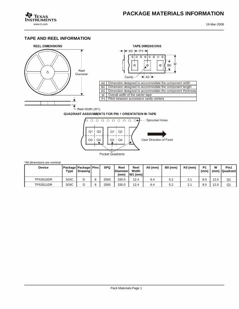
TAPE AND REEL INFORMATION
*All dimensions are nominal
Device PackageType
PackageDrawing
Pins SPQ ReelDiameter
(mm)
ReelWidth
W1 (mm)
A0 (mm) B0 (mm) K0 (mm) P1(mm)
W(mm)
Pin1Quadrant
TPS3510DR SOIC D 8 2500 330.0 12.4 6.4 5.2 2.1 8.0 12.0 Q1
TPS3511DR SOIC D 8 2500 330.0 12.4 6.4 5.2 2.1 8.0 12.0 Q1
PACKAGE MATERIALS INFORMATION
www.ti.com 19-Mar-2008
Pack Materials-Page 1

*All dimensions are nominal
Device Package Type Package Drawing Pins SPQ Length (mm) Width (mm) Height (mm)
TPS3510DR SOIC D 8 2500 340.5 338.1 20.6
TPS3511DR SOIC D 8 2500 340.5 338.1 20.6
PACKAGE MATERIALS INFORMATION
www.ti.com 19-Mar-2008
Pack Materials-Page 2


IMPORTANT NOTICETexas Instruments Incorporated and its subsidiaries (TI) reserve the right to make corrections, enhancements, improvements and otherchanges to its semiconductor products and services per JESD46, latest issue, and to discontinue any product or service per JESD48, latestissue. Buyers should obtain the latest relevant information before placing orders and should verify that such information is current andcomplete. All semiconductor products (also referred to herein as “components”) are sold subject to TI’s terms and conditions of salesupplied at the time of order acknowledgment.TI warrants performance of its components to the specifications applicable at the time of sale, in accordance with the warranty in TI’s termsand conditions of sale of semiconductor products. Testing and other quality control techniques are used to the extent TI deems necessaryto support this warranty. Except where mandated by applicable law, testing of all parameters of each component is not necessarilyperformed.TI assumes no liability for applications assistance or the design of Buyers’ products. Buyers are responsible for their products andapplications using TI components. To minimize the risks associated with Buyers’ products and applications, Buyers should provideadequate design and operating safeguards.TI does not warrant or represent that any license, either express or implied, is granted under any patent right, copyright, mask work right, orother intellectual property right relating to any combination, machine, or process in which TI components or services are used. Informationpublished by TI regarding third-party products or services does not constitute a license to use such products or services or a warranty orendorsement thereof. Use of such information may require a license from a third party under the patents or other intellectual property of thethird party, or a license from TI under the patents or other intellectual property of TI.Reproduction of significant portions of TI information in TI data books or data sheets is permissible only if reproduction is without alterationand is accompanied by all associated warranties, conditions, limitations, and notices. TI is not responsible or liable for such altereddocumentation. Information of third parties may be subject to additional restrictions.Resale of TI components or services with statements different from or beyond the parameters stated by TI for that component or servicevoids all express and any implied warranties for the associated TI component or service and is an unfair and deceptive business practice.TI is not responsible or liable for any such statements.Buyer acknowledges and agrees that it is solely responsible for compliance with all legal, regulatory and safety-related requirementsconcerning its products, and any use of TI components in its applications, notwithstanding any applications-related information or supportthat may be provided by TI. Buyer represents and agrees that it has all the necessary expertise to create and implement safeguards whichanticipate dangerous consequences of failures, monitor failures and their consequences, lessen the likelihood of failures that might causeharm and take appropriate remedial actions. Buyer will fully indemnify TI and its representatives against any damages arising out of the useof any TI components in safety-critical applications.In some cases, TI components may be promoted specifically to facilitate safety-related applications. With such components, TI’s goal is tohelp enable customers to design and create their own end-product solutions that meet applicable functional safety standards andrequirements. Nonetheless, such components are subject to these terms.No TI components are authorized for use in FDA Class III (or similar life-critical medical equipment) unless authorized officers of the partieshave executed a special agreement specifically governing such use.Only those TI components which TI has specifically designated as military grade or “enhanced plastic” are designed and intended for use inmilitary/aerospace applications or environments. Buyer acknowledges and agrees that any military or aerospace use of TI componentswhich have not been so designated is solely at the Buyer's risk, and that Buyer is solely responsible for compliance with all legal andregulatory requirements in connection with such use.TI has specifically designated certain components as meeting ISO/TS16949 requirements, mainly for automotive use. In any case of use ofnon-designated products, TI will not be responsible for any failure to meet ISO/TS16949.Products ApplicationsAudio www.ti.com/audio Automotive and Transportation www.ti.com/automotiveAmplifiers amplifier.ti.com Communications and Telecom www.ti.com/communicationsData Converters dataconverter.ti.com Computers and Peripherals www.ti.com/computersDLP® Products www.dlp.com Consumer Electronics www.ti.com/consumer-appsDSP dsp.ti.com Energy and Lighting www.ti.com/energyClocks and Timers www.ti.com/clocks Industrial www.ti.com/industrialInterface interface.ti.com Medical www.ti.com/medicalLogic logic.ti.com Security www.ti.com/securityPower Mgmt power.ti.com Space, Avionics and Defense www.ti.com/space-avionics-defenseMicrocontrollers microcontroller.ti.com Video and Imaging www.ti.com/videoRFID www.ti-rfid.comOMAP Applications Processors www.ti.com/omap TI E2E Community e2e.ti.comWireless Connectivity www.ti.com/wirelessconnectivity
Mailing Address: Texas Instruments, Post Office Box 655303, Dallas, Texas 75265Copyright © 2014, Texas Instruments Incorporated


![29005910 REV 002 PC-LINK[5sp] INIS EN](https://static.fdocuments.in/doc/165x107/625f378729467076573a2c50/29005910-rev-002-pc-link5sp-inis-en.jpg)