Towards wafer-size graphene layers by atmospheric …€¦ · LETTERS PUBLISHEDONLINE:8FEBRUARY2009...
5
LETTERS PUBLISHED ONLINE: 8 FEBRUARY 2009 DOI: 10.1038/NMAT2382 Towards wafer-size graphene layers by atmospheric pressure graphitization of silicon carbide Konstantin V. Emtsev 1 , Aaron Bostwick 2 , Karsten Horn 3 , Johannes Jobst 4 , Gary L. Kellogg 5 , Lothar Ley 1 , Jessica L. McChesney 2 , Taisuke Ohta 5 , Sergey A. Reshanov 4 , Jonas Röhrl 1 , Eli Rotenberg 2 , Andreas K. Schmid 6 , Daniel Waldmann 4 , Heiko B. Weber 4 and Thomas Seyller 1 * Graphene, a single monolayer of graphite, has recently attracted considerable interest owing to its novel magneto- transport properties 1–3 , high carrier mobility and ballistic transport up to room temperature 4 . It has the potential for technological applications as a successor of silicon in the post Moore’s law era 5–7 , as a single-molecule gas sensor 8 , in spintronics 9–11 , in quantum computing 12 or as a terahertz oscillator 13 . For such applications, uniform ordered growth of graphene on an insulating substrate is necessary. The growth of graphene on insulating silicon carbide (SiC) surfaces by high- temperature annealing in vacuum was previously proposed to open a route for large-scale production of graphene-based devices 5,6 . However, vacuum decomposition of SiC yields graphene layers with small grains (30–200 nm; refs 14–16). Here, we show that the ex situ graphitization of Si-terminated SiC(0001) in an argon atmosphere of about 1 bar produces monolayer graphene films with much larger domain sizes than previously attainable. Raman spectroscopy and Hall measurements confirm the improved quality of the films thus obtained. High electronic mobilities were found, which reach μ = 2,000 cm 2 V -1 s -1 at T = 27 K. The new growth process introduced here establishes a method for the synthesis of graphene films on a technologically viable basis. The successful development of graphene-based electronic devices depends on a large-scale availability of the material. Several methods for graphene production have been proposed. Mechanical exfoliation 17 leads to isolated, high-quality crystals with dimensions only in the 10 μm range, which questions the practicality of this method. Large, high-quality graphene islands were grown on the surface of transition metals such as Ru(0001) (ref. 18), but this technique requires transfer to an insulating substrate, with methods that have yet to be developed. Liquid-phase exfoliation 19 yields high quantities of monolayer and few-layer graphene. Although this method—in contrast to graphene oxide reduction 20 —prevents the formation of defects, the electrical properties are similar to graphene oxide reduction, indicating poor transport at contacts between the individual graphene sheets. The preparation of single-layer graphene by the thermal decomposition of silicon carbide (SiC) has been proposed as a viable route for the synthesis of uniform, wafer-size graphene layers 1 Lehrstuhl für Technische Physik, Friedrich-Alexander-Universität Erlangen-Nürnberg, Erwin-Rommel-Str. 1, 91058 Erlangen, Germany, 2 Advanced Light Source, Lawrence Berkeley National Laboratory, One Cyclotron Road, Berkeley, California 94720, USA, 3 Department of Molecular Physics, Fritz-Haber-Institut der Max-Planck-Gesellschaft, Faradayweg 4-6, 14195 Berlin, Germany, 4 Lehrstuhl für Angewandte Physik, Friedrich-Alexander-Universität Erlangen-Nürnberg, Staudtstr. 7, 91058 Erlangen, Germany, 5 Sandia National Laboratories, Surface & Interface Sciences Department, PO Box 5800, Albuquerque, New Mexico 87185, USA, 6 National Center for Electron Microscopy, Lawrence Berkeley National Laboratory, One Cyclotron Road, Berkeley, California 94720, USA. *e-mail: [email protected]. for technological applications 5–7 . A considerable advantage of this method is that insulating SiC substrates can be used so that transfer to another insulator is not required. However, the large-scale structural quality is limited at present by the lack of continuity and uniformity of the grown film 15,16 . On the Si-terminated (0001) basal plane, vacuum annealing leads to small graphene domains typically 30–100 nm in diameter, whereas on the C-terminated (000 ¯ 1) face, larger domains (∼200 nm) of multilayered, rotationally disordered graphene have been produced 14 . The small-grain structure is due to morphological changes of the surface in the course of high-temperature annealing. Moreover, decomposition of SiC is not a self-limiting process and, as a result, regions of different film thicknesses coexist, as shown by low-energy electron microscopy 15,16 (LEEM). Such inhomogeneous films do not meet the demands of large-scale device production, which requires larger domains and tighter thickness control. Homogeneous film thickness is particularly important because the electronic structure of the film depends strongly on the number of layers. For example, although monolayer graphene is a gapless semiconductor, a forbidden gap can be induced in bilayer graphene and tuned by an external electrostatic potential 21,22 . Here we demonstrate a method of preparing graphene on SiC(0001) that results in a significantly improved film quality. In Fig. 1, we compare samples prepared by vacuum annealing with samples produced by ex situ annealing under an argon atmosphere. Figure 1a–c shows the morphology of the 6H–SiC(0001) surface before and after the formation of a graphene monolayer by annealing in ultrahigh vacuum (UHV) as determined by atomic force microscopy (AFM) and LEEM. The initial 6H–SiC(0001) surface in Fig. 1a, obtained after hydrogen etching, is characterized by wide, highly uniform, atomically flat terraces. The step direction and terrace width (of the order of 300–700 nm) are determined by the incidental misorientation of the substrate surface with respect to the crystallographic (0001) plane. The step height is 1.5 nm, which corresponds to the dimension of the 6H–SiC unit cell in the direction perpendicular to the surface (c axis). On defect-free areas of the sample, the terraces typically extend undisturbed over 50 μm in length. The morphology of the surface covered with a monolayer of graphene prepared by vacuum annealing is shown in Fig. 1b. The surface obviously undergoes significant modifications; it is now covered with small pits up to 10 nm in depth, and the original NATURE MATERIALS | VOL 8 | MARCH 2009 | www.nature.com/naturematerials 203
Transcript of Towards wafer-size graphene layers by atmospheric …€¦ · LETTERS PUBLISHEDONLINE:8FEBRUARY2009...

LETTERSPUBLISHED ONLINE: 8 FEBRUARY 2009 DOI: 10.1038/NMAT2382
Towards wafer-size graphene layers by atmosphericpressure graphitization of silicon carbideKonstantin V. Emtsev1, Aaron Bostwick2, Karsten Horn3, Johannes Jobst4, Gary L. Kellogg5,Lothar Ley1, Jessica L. McChesney2, Taisuke Ohta5, Sergey A. Reshanov4, Jonas Röhrl1,Eli Rotenberg2, Andreas K. Schmid6, Daniel Waldmann4, Heiko B. Weber4 and Thomas Seyller1*Graphene, a single monolayer of graphite, has recentlyattracted considerable interest owing to its novel magneto-transport properties1–3, high carrier mobility and ballistictransport up to room temperature4. It has the potential fortechnological applications as a successor of silicon in thepost Moore’s law era5–7, as a single-molecule gas sensor8,in spintronics9–11, in quantum computing12 or as a terahertzoscillator13. For such applications, uniform ordered growth ofgraphene on an insulating substrate is necessary. The growth ofgraphene on insulating silicon carbide (SiC) surfaces by high-temperature annealing in vacuum was previously proposedto open a route for large-scale production of graphene-baseddevices5,6. However, vacuum decomposition of SiC yieldsgraphene layers with small grains (30–200 nm; refs 14–16).Here, we show that the ex situ graphitization of Si-terminatedSiC(0001) in an argon atmosphere of about 1 bar producesmonolayer graphene films with much larger domain sizesthan previously attainable. Raman spectroscopy and Hallmeasurements confirm the improved quality of the films thusobtained. High electronic mobilities were found, which reachµ = 2,000 cm 2 V−1 s−1 at T = 27 K. The new growth processintroduced here establishes a method for the synthesis ofgraphene films on a technologically viable basis.
The successful development of graphene-based electronicdevices depends on a large-scale availability of the material.Several methods for graphene production have been proposed.Mechanical exfoliation17 leads to isolated, high-quality crystalswith dimensions only in the 10 µm range, which questionsthe practicality of this method. Large, high-quality grapheneislands were grown on the surface of transition metals suchas Ru(0001) (ref. 18), but this technique requires transfer toan insulating substrate, with methods that have yet to bedeveloped. Liquid-phase exfoliation19 yields high quantities ofmonolayer and few-layer graphene. Although this method—incontrast to graphene oxide reduction20—prevents the formationof defects, the electrical properties are similar to graphene oxidereduction, indicating poor transport at contacts between theindividual graphene sheets.
The preparation of single-layer graphene by the thermaldecomposition of silicon carbide (SiC) has been proposed as aviable route for the synthesis of uniform, wafer-size graphene layers
1Lehrstuhl für Technische Physik, Friedrich-Alexander-Universität Erlangen-Nürnberg, Erwin-Rommel-Str. 1, 91058 Erlangen, Germany, 2Advanced LightSource, Lawrence Berkeley National Laboratory, One Cyclotron Road, Berkeley, California 94720, USA, 3Department of Molecular Physics,Fritz-Haber-Institut der Max-Planck-Gesellschaft, Faradayweg 4-6, 14195 Berlin, Germany, 4Lehrstuhl für Angewandte Physik,Friedrich-Alexander-Universität Erlangen-Nürnberg, Staudtstr. 7, 91058 Erlangen, Germany, 5Sandia National Laboratories, Surface & Interface SciencesDepartment, PO Box 5800, Albuquerque, New Mexico 87185, USA, 6National Center for Electron Microscopy, Lawrence Berkeley National Laboratory,One Cyclotron Road, Berkeley, California 94720, USA. *e-mail: [email protected].
for technological applications5–7. A considerable advantage of thismethod is that insulating SiC substrates can be used so that transferto another insulator is not required. However, the large-scalestructural quality is limited at present by the lack of continuityand uniformity of the grown film15,16. On the Si-terminated (0001)basal plane, vacuum annealing leads to small graphene domainstypically 30–100 nm in diameter, whereas on the C-terminated(0001̄) face, larger domains (∼200 nm) ofmultilayered, rotationallydisordered graphene have been produced14. The small-grainstructure is due to morphological changes of the surface in thecourse of high-temperature annealing. Moreover, decompositionof SiC is not a self-limiting process and, as a result, regions ofdifferent film thicknesses coexist, as shown by low-energy electronmicroscopy15,16 (LEEM). Such inhomogeneous films do not meetthe demands of large-scale device production, which requireslarger domains and tighter thickness control. Homogeneous filmthickness is particularly important because the electronic structureof the film depends strongly on the number of layers. Forexample, althoughmonolayer graphene is a gapless semiconductor,a forbidden gap can be induced in bilayer graphene and tuned byan external electrostatic potential21,22.
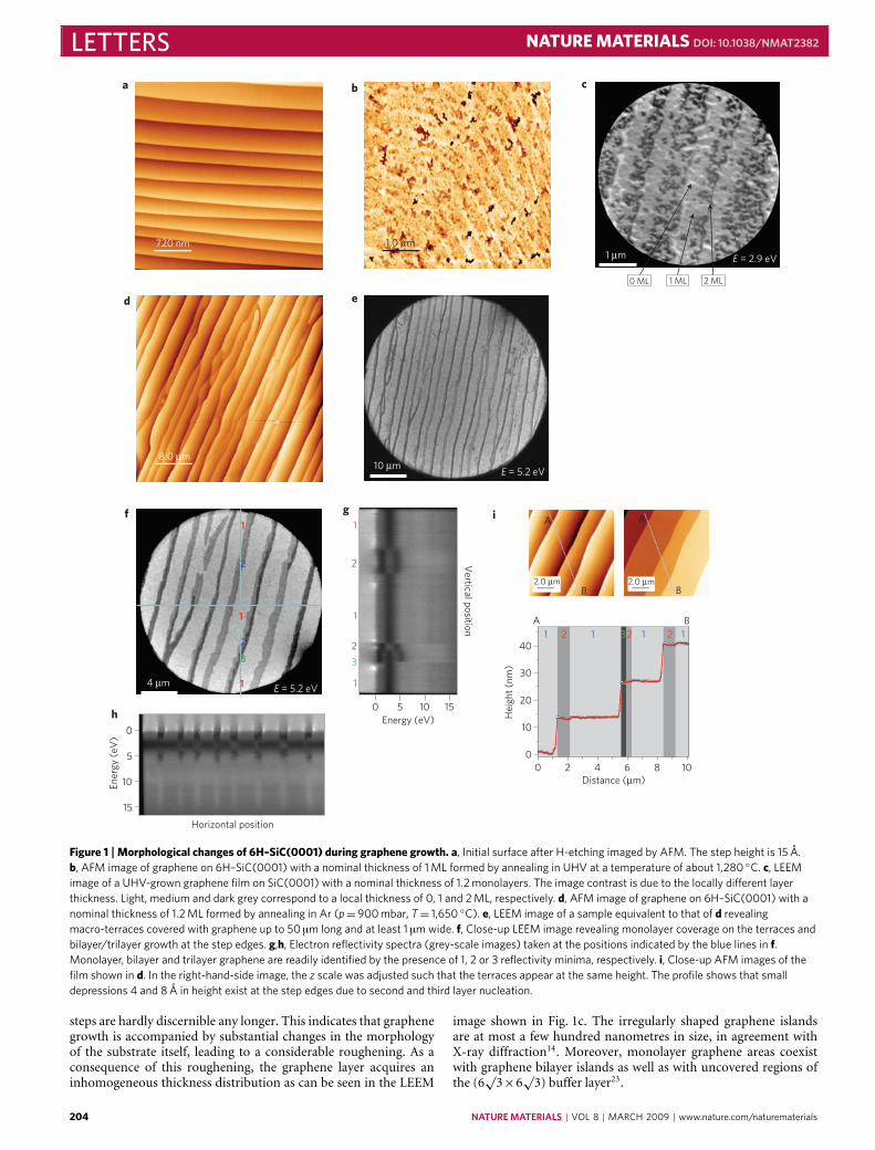
Here we demonstrate a method of preparing graphene onSiC(0001) that results in a significantly improved film quality. InFig. 1, we compare samples prepared by vacuum annealing withsamples produced by ex situ annealing under an argon atmosphere.Figure 1a–c shows the morphology of the 6H–SiC(0001) surfacebefore and after the formation of a graphene monolayer byannealing in ultrahigh vacuum (UHV) as determined by atomicforce microscopy (AFM) and LEEM. The initial 6H–SiC(0001)surface in Fig. 1a, obtained after hydrogen etching, is characterizedby wide, highly uniform, atomically flat terraces. The step directionand terrace width (of the order of 300–700 nm) are determined bythe incidental misorientation of the substrate surface with respectto the crystallographic (0001) plane. The step height is 1.5 nm,which corresponds to the dimension of the 6H–SiC unit cell in thedirection perpendicular to the surface (c axis). On defect-free areasof the sample, the terraces typically extend undisturbed over 50 µmin length. The morphology of the surface covered with a monolayerof graphene prepared by vacuum annealing is shown in Fig. 1b.The surface obviously undergoes significantmodifications; it is nowcovered with small pits up to 10 nm in depth, and the original
NATUREMATERIALS | VOL 8 | MARCH 2009 | www.nature.com/naturematerials 203
LETTERS NATURE MATERIALS DOI: 10.1038/NMAT2382
720 nm
1 ML 2 ML0 ML
E = 2.9 eV
E = 5.2 eV
1
2
3
2
1
1
Vertical position
A A
B B
B111 22 21 3
Hei
ght (
nm)
A
15
10
5
0
Horizontal position
Energy (eV)
Ener
gy (
eV)
4 µm
10 µm8.0 µm
1.0 µm
1
2
3
2
1
1
151050
1 µm
2.0 µm 2.0 µm
00 2 4 6
Distance (µm)8 10
10
20
30
40
a b c
d
g i
h
e
f
E = 5.2 eV
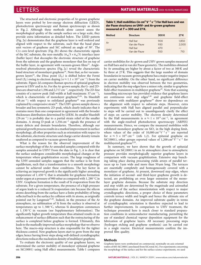
Figure 1 |Morphological changes of 6H–SiC(0001) during graphene growth. a, Initial surface after H-etching imaged by AFM. The step height is 15 Å.b, AFM image of graphene on 6H–SiC(0001) with a nominal thickness of 1 ML formed by annealing in UHV at a temperature of about 1,280 ◦C. c, LEEMimage of a UHV-grown graphene film on SiC(0001) with a nominal thickness of 1.2 monolayers. The image contrast is due to the locally different layerthickness. Light, medium and dark grey correspond to a local thickness of 0, 1 and 2 ML, respectively. d, AFM image of graphene on 6H–SiC(0001) with anominal thickness of 1.2 ML formed by annealing in Ar (p=900 mbar, T= 1,650 ◦C). e, LEEM image of a sample equivalent to that of d revealingmacro-terraces covered with graphene up to 50 µm long and at least 1 µm wide. f, Close-up LEEM image revealing monolayer coverage on the terraces andbilayer/trilayer growth at the step edges. g,h, Electron reflectivity spectra (grey-scale images) taken at the positions indicated by the blue lines in f.Monolayer, bilayer and trilayer graphene are readily identified by the presence of 1, 2 or 3 reflectivity minima, respectively. i, Close-up AFM images of thefilm shown in d. In the right-hand-side image, the z scale was adjusted such that the terraces appear at the same height. The profile shows that smalldepressions 4 and 8 Å in height exist at the step edges due to second and third layer nucleation.
steps are hardly discernible any longer. This indicates that graphenegrowth is accompanied by substantial changes in the morphologyof the substrate itself, leading to a considerable roughening. As aconsequence of this roughening, the graphene layer acquires aninhomogeneous thickness distribution as can be seen in the LEEM
image shown in Fig. 1c. The irregularly shaped graphene islandsare at most a few hundred nanometres in size, in agreement withX-ray diffraction14. Moreover, monolayer graphene areas coexistwith graphene bilayer islands as well as with uncovered regions ofthe (6
√3×6√3) buffer layer23.
204 NATUREMATERIALS | VOL 8 | MARCH 2009 | www.nature.com/naturematerials

NATURE MATERIALS DOI: 10.1038/NMAT2382 LETTERS
288 287 286 285Binding energy (eV)
Inte
nsity
(ar
b. u
nits
)
284 283 282
S2
S1
G
SiC
ED
1.5
Bind
ing
ener
gy (
eV)
1.6 1.7Electron momentum Kll (Ŭ1)
1.8 1.91.5
1.0
0.5
0
1,400
Inte
nsity
(ar
b. u
nits
)
1,600 1,800Raman shift (cm¬1)
2,600 2,800
G-peak
2D-peak
D-peak(1,356 ± 5) cm¬1
(1,596 ± 5) cm¬1(2,717 ± 5) cm¬1
(1,592 ± 5) cm¬1
(2,706 ± 5) cm¬1
54 cm¬1
37 cm¬1
a b
c d
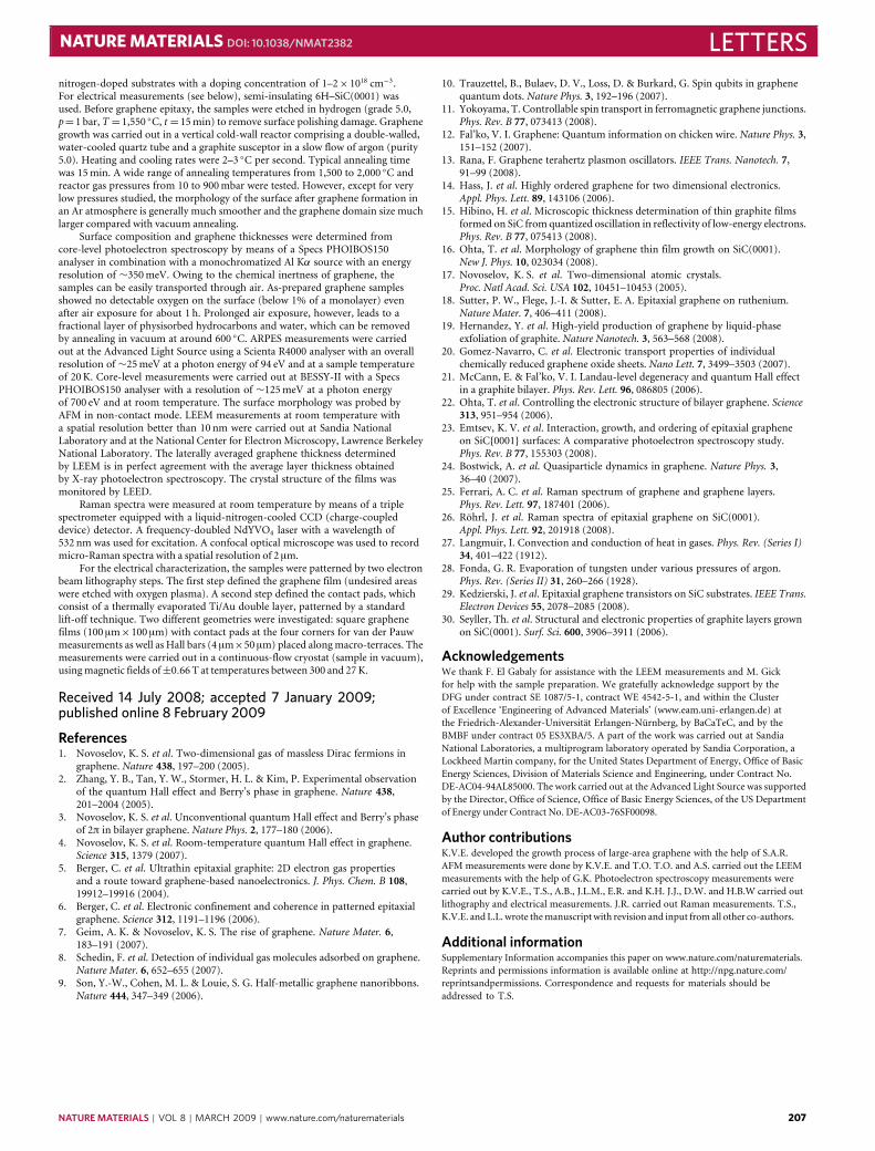
Figure 2 |Atomic and electronic structure of ex-situ-grown monolayer graphene. a, LEED pattern at 74 eV showing the diffraction spots dueto the SiC(0001) substrate (blue arrows) and the graphene lattice (red arrows). The extra spots are due to the (6
√3×6√
3) interface layer. b, C1score-level spectrum measured at a photon energy of 700 eV. The spectrum contains contributions from the SiC substrate (marked SiC), the (6
√3×6√
3)interface layer (marked S1 and S2) and from the graphene layer (G) residing on top of the interface layer. c, π-bands probed by ARPES in the vicinity of theK-point of the hexagonal Brillouin zone measured along the 0 K-direction. The position of the Dirac energy (ED) at 0.45 eV below the Fermi energy isconsistent with previous reports on UHV-grown graphene on SiC(0001). Faint features marked by yellow arrows signal the presence of small regions ofbilayer graphene in agreement with the LEEM results. d, Comparison of Raman spectra of Ar-grown (red) and UHV-grown (blue) epitaxial graphene on6H–SiC(0001). The spectra of the D- and G-line shown here are corrected for the emission of the substrate by subtraction of a reference spectrum26
(see Supplementary Information).
In stark contrast to the low quality resulting from vacuumgraphitization (Fig. 1b), films grown under 900mbar of argon havea greatly improved surface morphology, as demonstrated by theAFM image in Fig. 1d. Large continuous terraces are found, extend-ing over large distances parallel to the step edges. Step bunching ismanifested by the formation of macro-terraces that are a factor of5–8 times wider than the original terraces. Themacro-steps are par-allel to the original steps, increase in step height by the same factorand reach average heights of 8–15 nm. Parallel to the steps, uninter-ruptedmacro-terracesmore than 50 µmlong have been observed.
The thickness distribution of the graphene film grown under anargon atmosphere is determined by LEEM as shown in Fig. 1e,f.A series of spatially resolved LEEM I–V spectra taken along avertical and a horizontal line in Fig. 1f is shown in Fig. 1g,h. Thelayer thickness is easily determined from the number of minimain the individual spectra; the LEEM image taken at a particular
energy shows stripes that follow in width and orientation themacro-terraces with a contrast that is determined by the graphenelayer thickness15,16. Hence, we can unambiguously conclude thatexcept for narrow stripes at the edges, the large atomicallyflat macro-terraces are homogeneously covered with a graphenemonolayer. The domain size of monolayer graphene is significantlylarger than that of the vacuum-annealed samples as a comparisonbetween Fig. 1c,f shows. In fact, the domain size seems to belimited only by the length and width of the SiC terraces. Narrower,darker regions at the downward edges of the terraces correspondto bilayer and in some cases trilayer graphene (see region 3 inFig. 1f). In the AFM image, these regions (see Fig. 1i) appearas small depressions of around 0.5 nm and 1 nm amplitudelocated at the very edge of the macro-step. This indicates thatthe nucleation of new graphene layers starts at step edges ofthe substrate surface.
NATUREMATERIALS | VOL 8 | MARCH 2009 | www.nature.com/naturematerials 205
LETTERS NATURE MATERIALS DOI: 10.1038/NMAT2382
The structural and electronic properties of Ar-grown graphenelayers were probed by low-energy electron diffraction (LEED),photoelectron spectroscopy and Raman spectroscopy as shownin Fig. 2. Although these methods alone cannot assess themorphological quality of the sample surface on a large scale, theyprovide extra information as detailed below. The LEED pattern(Fig. 2a) demonstrates that the graphene layer is well ordered andaligned with respect to the substrate, such that the basal planeunit vectors of graphene and SiC subtend an angle of 30◦. TheC1s core-level spectrum (Fig. 2b) shows the characteristic signalsof the SiC substrate, the non-metallic (6
√3×6√3) interface layer
(buffer layer) that decouples the electronic structure of graphenefrom the substrate and the graphene monolayer that lies on top ofthe buffer layer, in agreement with vacuum-grown films23. Angle-resolved photoelectron spectra (Fig. 2c) reveal the characteristicband structure of monolayer graphene24. Note that, as for vacuum-grown layers24, the Dirac point (ED) is shifted below the Fermilevel (EF) owing to electron doping (n≈ 1.1×1013 cm−2) from thesubstrate. Figure 2d compares Raman spectra of epitaxial graphenegrown in UHV and in Ar. For the Ar-grown sample, the G- and 2D-lines are observed at 1,596 and 2,717 cm−1, respectively. The 2D-lineconsists of a narrow peak (full-width at half-maximum: 37 cm−1),which is characteristic of monolayer graphene25,26. Its blueshift(38 cm−1) with respect to exfoliated graphene25 was previouslyexplained by compressive strain26. TheUHV-grown sample shows abroader and less symmetric 2D-peak, which clearly indicates that itcontains more than one component in agreement with the broaderthicknesses distribution determined by LEEM. Its smaller blueshift(29 cm−1) is probably due to a partial strain relief of the smallerdomains. A strong D-peak at 1,356 cm−1 signals the presence ofmany defects and domain boundaries. Therefore, although ourepitaxial growth process results in amarked improvement in surfacemorphology, all other properties such as orientation with respect tothe substrate, electronic structure and charge carrier density remainunaltered as compared to vacuum-grown layers.
What is the reason for the observed improvement of thesurface morphology of the Ar-annealed samples compared with thesamples annealed in UHV? From the data in Fig. 1, it is clear thatthe surface undergoes considerable morphological changes at thetemperature where graphitization occurs. The large roughness ofthe UHV-annealed samples suggests that the surface is far fromequilibrium, such that a transformation to a smooth morphologycannot be achieved under these conditions. The key factor inachieving an improved growth is the significantly higher annealingtemperature of 1,650 ◦C that is attainable for graphene formationunder argon at a pressure of 900mbar as compared with 1,280 ◦C inUHV. Graphene formation is the result of Si evaporation from thesubstrate. For a given temperature, the presence of a high pressureof argon leads to a reduced Si evaporation rate because the siliconatoms desorbing from the surface have a finite probability of beingreflected back to the surface by collision with Ar atoms, as originallypointed out by Langmuir27,28. Indeed, in the presence of the Aratmosphere, no sublimation of Si from the surface is observed attemperatures up to 1,500 ◦C, whereas Si desorption commencesat 1,150 ◦C in vacuum (see Supplementary Information). Thesignificantly higher growth temperature thus attained results in anenhancement of surface diffusion such that the restructuring of thesurface is completed before graphene is formed. Ultimately, thisleads to themarkedly improved surfacemorphology thatwe observehere. The macro-step structure is also responsible for the tighterthickness control. New graphene layers start to grow from the stepedges; hence having fewer steps along well-defined crystallographicdirections reduces the nucleation density ofmultilayer graphene.
To evaluate the electronic quality of our graphene layers, wedetermined the carrier mobility of monolayer epitaxial grapheneon SiC(0001) using Hall effect measurements. Table 1 compares
Table 1 |Hall mobilities (in cm2 V−1 s−1) for Hall bars and vander Pauw structures on UHV- and Ar-grown graphenemeasured at T= 300 and 27 K.
Method Structure 300K 27K
ArHall bar 900 1,850Van der Pauw 930 2,000
UHVHall bar 470 —Van der Pauw 550 710
carriermobilities for Ar-grown andUHV-grown samplesmeasuredonHall bars and in van der Pauw geometry. Themobilities obtainedby Ar annealing are higher by about a factor of two at 300K andby three at 27 K. This suggests that the large number of domainboundaries in vacuum-grown graphene has amajor negative impacton carrier mobility. On the other hand, no significant differencein electron mobility was observed between the two geometries,indicating that the step edges have a minor role, similar to graphenefield-effect transistors in multilayer graphene29. Note that scanningtunnelling microscopy has provided evidence that graphene layersare continuous over step edges5,30 and graphene field-effecttransistors with multilayer graphene29 show no dependence onthe alignment with respect to substrate steps. However, extraexperiments with Hall bars aligned parallel and perpendicularto steps will be carried out to unambiguously clarify the effectof steps on carrier mobility. The electron density determinedby the Hall measurements is n ≈ 1 × 1013 cm−2, in agreementwith the angle-resolved photoelectron spectroscopy (ARPES)measurements. Hence, we compare the measured mobilities withexfoliated monolayer graphene on SiO2 in the high doping limit,where values of the order of 10,000 cm2 V−1 s−1 are reportedfor n ≈ 5 × 1012 cm−2 (refs 1,2). For epitaxial graphene onSiC(0001), other groups reported values of 1,200 cm2 V−1 s−1 formultilayered graphene5,29.
In summary, we have shown that the growth of epitaxialgraphene on SiC(0001) in an Ar atmosphere close to atmosphericpressure provides morphologically superior graphene layers incomparison with vacuum graphitization. Extensive step bunch-ing taking place during processing yields arrays of parallel ter-races up to 3 µm wide and more than 50 µm long. The terracesare essentially completely and homogeneously covered with amonolayer of graphene. At present, downward step edges, wherethe initiation of second- and third-layer graphene growth is de-tected, are prohibiting an even larger extension of the mono-layer graphene domains. Because the substrate step directionand step width are determined by the magnitude and azimuthalorientation of the surface misorientation with respect to majorcrystallographic directions, a proper choice of these parameterscontrols terrace width and length and hence the ultimate size ofthe graphene domains. An improved substrate quality in termsof crystallographic orientation is therefore expected to lead tofurther improvements. In comparison to UHV treatment, thetechnique presented here is much closer to standard prepara-tion conditions in semiconductor manufacturing, permitting theuse of standard chemical vapour deposition equipment for thefabrication of graphene layers. All necessary processing steps(hydrogen etching and graphene synthesis) can be carried outin a single reactor. Electrical measurements confirm the im-proved film quality.
MethodsGraphene layers were synthesized on commercial, nominally on-axis orientedwafers of 6H–SiC(0001) purchased from SiCrystal AG. For experiments concerningthe morphology of the surface and for the surface science experiments, we used
206 NATUREMATERIALS | VOL 8 | MARCH 2009 | www.nature.com/naturematerials
NATURE MATERIALS DOI: 10.1038/NMAT2382 LETTERSnitrogen-doped substrates with a doping concentration of 1–2× 1018 cm−3.For electrical measurements (see below), semi-insulating 6H–SiC(0001) wasused. Before graphene epitaxy, the samples were etched in hydrogen (grade 5.0,p=1 bar, T =1,550 ◦C, t =15min) to remove surface polishing damage. Graphenegrowth was carried out in a vertical cold-wall reactor comprising a double-walled,water-cooled quartz tube and a graphite susceptor in a slow flow of argon (purity5.0). Heating and cooling rates were 2–3 ◦C per second. Typical annealing timewas 15min. A wide range of annealing temperatures from 1,500 to 2,000 ◦C andreactor gas pressures from 10 to 900mbar were tested. However, except for verylow pressures studied, the morphology of the surface after graphene formation inan Ar atmosphere is generally much smoother and the graphene domain size muchlarger compared with vacuum annealing.
Surface composition and graphene thicknesses were determined fromcore-level photoelectron spectroscopy by means of a Specs PHOIBOS150analyser in combination with a monochromatized Al Kα source with an energyresolution of ∼350meV. Owing to the chemical inertness of graphene, thesamples can be easily transported through air. As-prepared graphene samplesshowed no detectable oxygen on the surface (below 1% of a monolayer) evenafter air exposure for about 1 h. Prolonged air exposure, however, leads to afractional layer of physisorbed hydrocarbons and water, which can be removedby annealing in vacuum at around 600 ◦C. ARPES measurements were carriedout at the Advanced Light Source using a Scienta R4000 analyser with an overallresolution of ∼25meV at a photon energy of 94 eV and at a sample temperatureof 20 K. Core-level measurements were carried out at BESSY-II with a SpecsPHOIBOS150 analyser with a resolution of ∼125meV at a photon energyof 700 eV and at room temperature. The surface morphology was probed byAFM in non-contact mode. LEEM measurements at room temperature witha spatial resolution better than 10 nm were carried out at Sandia NationalLaboratory and at the National Center for Electron Microscopy, Lawrence BerkeleyNational Laboratory. The laterally averaged graphene thickness determinedby LEEM is in perfect agreement with the average layer thickness obtainedby X-ray photoelectron spectroscopy. The crystal structure of the films wasmonitored by LEED.
Raman spectra were measured at room temperature by means of a triplespectrometer equipped with a liquid-nitrogen-cooled CCD (charge-coupleddevice) detector. A frequency-doubled NdYVO4 laser with a wavelength of532 nm was used for excitation. A confocal optical microscope was used to recordmicro-Raman spectra with a spatial resolution of 2 µm.
For the electrical characterization, the samples were patterned by two electronbeam lithography steps. The first step defined the graphene film (undesired areaswere etched with oxygen plasma). A second step defined the contact pads, whichconsist of a thermally evaporated Ti/Au double layer, patterned by a standardlift-off technique. Two different geometries were investigated: square graphenefilms (100 µm×100 µm) with contact pads at the four corners for van der Pauwmeasurements as well as Hall bars (4 µm×50 µm) placed alongmacro-terraces. Themeasurements were carried out in a continuous-flow cryostat (sample in vacuum),usingmagnetic fields of±0.66 T at temperatures between 300 and 27K.
Received 14 July 2008; accepted 7 January 2009;published online 8 February 2009
References1. Novoselov, K. S. et al. Two-dimensional gas of massless Dirac fermions in
graphene. Nature 438, 197–200 (2005).2. Zhang, Y. B., Tan, Y. W., Stormer, H. L. & Kim, P. Experimental observation
of the quantum Hall effect and Berry’s phase in graphene. Nature 438,201–2004 (2005).
3. Novoselov, K. S. et al. Unconventional quantum Hall effect and Berry’s phaseof 2π in bilayer graphene. Nature Phys. 2, 177–180 (2006).
4. Novoselov, K. S. et al. Room-temperature quantum Hall effect in graphene.Science 315, 1379 (2007).
5. Berger, C. et al. Ultrathin epitaxial graphite: 2D electron gas propertiesand a route toward graphene-based nanoelectronics. J. Phys. Chem. B 108,19912–19916 (2004).
6. Berger, C. et al. Electronic confinement and coherence in patterned epitaxialgraphene. Science 312, 1191–1196 (2006).
7. Geim, A. K. & Novoselov, K. S. The rise of graphene. Nature Mater. 6,183–191 (2007).
8. Schedin, F. et al. Detection of individual gas molecules adsorbed on graphene.Nature Mater. 6, 652–655 (2007).
9. Son, Y.-W., Cohen, M. L. & Louie, S. G. Half-metallic graphene nanoribbons.Nature 444, 347–349 (2006).
10. Trauzettel, B., Bulaev, D. V., Loss, D. & Burkard, G. Spin qubits in graphenequantum dots. Nature Phys. 3, 192–196 (2007).
11. Yokoyama, T. Controllable spin transport in ferromagnetic graphene junctions.Phys. Rev. B 77, 073413 (2008).
12. Fal’ko, V. I. Graphene: Quantum information on chicken wire. Nature Phys. 3,151–152 (2007).
13. Rana, F. Graphene terahertz plasmon oscillators. IEEE Trans. Nanotech. 7,91–99 (2008).
14. Hass, J. et al. Highly ordered graphene for two dimensional electronics.Appl. Phys. Lett. 89, 143106 (2006).
15. Hibino, H. et al. Microscopic thickness determination of thin graphite filmsformed on SiC from quantized oscillation in reflectivity of low-energy electrons.Phys. Rev. B 77, 075413 (2008).
16. Ohta, T. et al. Morphology of graphene thin film growth on SiC(0001).New J. Phys. 10, 023034 (2008).
17. Novoselov, K. S. et al. Two-dimensional atomic crystals.Proc. Natl Acad. Sci. USA 102, 10451–10453 (2005).
18. Sutter, P. W., Flege, J.-I. & Sutter, E. A. Epitaxial graphene on ruthenium.Nature Mater. 7, 406–411 (2008).
19. Hernandez, Y. et al. High-yield production of graphene by liquid-phaseexfoliation of graphite. Nature Nanotech. 3, 563–568 (2008).
20. Gomez-Navarro, C. et al. Electronic transport properties of individualchemically reduced graphene oxide sheets. Nano Lett. 7, 3499–3503 (2007).
21. McCann, E. & Fal’ko, V. I. Landau-level degeneracy and quantum Hall effectin a graphite bilayer. Phys. Rev. Lett. 96, 086805 (2006).
22. Ohta, T. et al. Controlling the electronic structure of bilayer graphene. Science313, 951–954 (2006).
23. Emtsev, K. V. et al. Interaction, growth, and ordering of epitaxial grapheneon SiC{0001} surfaces: A comparative photoelectron spectroscopy study.Phys. Rev. B 77, 155303 (2008).
24. Bostwick, A. et al. Quasiparticle dynamics in graphene. Nature Phys. 3,36–40 (2007).
25. Ferrari, A. C. et al. Raman spectrum of graphene and graphene layers.Phys. Rev. Lett. 97, 187401 (2006).
26. Röhrl, J. et al. Raman spectra of epitaxial graphene on SiC(0001).Appl. Phys. Lett. 92, 201918 (2008).
27. Langmuir, I. Convection and conduction of heat in gases. Phys. Rev. (Series I)34, 401–422 (1912).
28. Fonda, G. R. Evaporation of tungsten under various pressures of argon.Phys. Rev. (Series II) 31, 260–266 (1928).
29. Kedzierski, J. et al. Epitaxial graphene transistors on SiC substrates. IEEE Trans.Electron Devices 55, 2078–2085 (2008).
30. Seyller, Th. et al. Structural and electronic properties of graphite layers grownon SiC(0001). Surf. Sci. 600, 3906–3911 (2006).
AcknowledgementsWe thank F. El Gabaly for assistance with the LEEM measurements and M. Gickfor help with the sample preparation. We gratefully acknowledge support by theDFG under contract SE 1087/5-1, contract WE 4542-5-1, and within the Clusterof Excellence ‘Engineering of Advanced Materials’ (www.eam.uni-erlangen.de) atthe Friedrich-Alexander-Universität Erlangen-Nürnberg, by BaCaTeC, and by theBMBF under contract 05 ES3XBA/5. A part of the work was carried out at SandiaNational Laboratories, a multiprogram laboratory operated by Sandia Corporation, aLockheed Martin company, for the United States Department of Energy, Office of BasicEnergy Sciences, Division of Materials Science and Engineering, under Contract No.DE-AC04-94AL85000. The work carried out at the Advanced Light Source was supportedby the Director, Office of Science, Office of Basic Energy Sciences, of the US Departmentof Energy under Contract No. DE-AC03-76SF00098.
Author contributionsK.V.E. developed the growth process of large-area graphene with the help of S.A.R.AFM measurements were done by K.V.E. and T.O. T.O. and A.S. carried out the LEEMmeasurements with the help of G.K. Photoelectron spectroscopy measurements werecarried out by K.V.E., T.S., A.B., J.L.M., E.R. and K.H. J.J., D.W. and H.B.W carried outlithography and electrical measurements. J.R. carried out Raman measurements. T.S.,K.V.E. and L.L. wrote themanuscriptwith revision and input fromall other co-authors.
Additional informationSupplementary Information accompanies this paper on www.nature.com/naturematerials.Reprints and permissions information is available online at http://npg.nature.com/reprintsandpermissions. Correspondence and requests for materials should beaddressed to T.S.
NATUREMATERIALS | VOL 8 | MARCH 2009 | www.nature.com/naturematerials 207