TOPICAL REVIEW Micro-Raman spectroscopy to study … · TOPICAL REVIEW Micro-Raman spectroscopy to...
16
Semicond. Sci. Technol. 11 (1996) 139–154. Printed in the UK TOPICAL REVIEW Micro-Raman spectroscopy to study local mechanical stress in silicon integrated circuits Ingrid De Wolf Interuniversity Micro-Electronics Center (IMEC), Kapeldreef 75, B-3001 Leuven, Belgium Received 19 July 1995, accepted for publication 2 October 1995 Abstract. Local mechanical stress is currently an important topic of concern in microelectronics processing. A technique that has become increasingly popular for local mechanical stress measurements is micro-Raman spectroscopy. In this paper, the theoretical background of Raman spectroscopy, with special attention to its sensitivity for mechanical stress, is discussed, and practical information is given for the application of this technique to stress measurements in silicon integrated circuits. An overview is given of some important applications of the technique, illustrated with examples from the literature: the first studies of the influence of external stress on the Si Raman modes are reviewed; the application of this technique to measure stress in silicon-on-insulator films is discussed; results of measurements of local stress in isolation structures and trenches are reviewed; and the use of micro-Raman spectroscopy to obtain more information on stress in metals, by measuring the stress in the surrounding Si substrate is explained. 1. Introduction Silicon integrated circuits constitute a complex mosaic, where materials with different characteristics, grown or deposited in different ways and at different temperatures, are linked together in various geometries. It is well known that during and after processing of these devices, mechanical stresses develop in the films and in the substrate. These stresses may be due to thermal steps, for example when there is a difference in thermal expansion coefficient or when the temperature distribution across the wafer is non-uniform; due to intrinsic stresses which are inherent in the formation process of the film, for example in chemical vapour deposited silicon nitride; or due to the geometry of the material, for example high stresses are present in the substrate at film edges. Large stresses can also be induced in the substrate near embedded structures such as trenches; and also the non-planar growth of materials, as for example the field oxide in local oxidation, induces large stresses in the surrounding substrate. The problems associated with these stresses are very divergent. Stress may directly trigger the nucleation and propagation of dislocations and the formation of voids and cracks [1]. For example, poly-Si grain regrowth during annealling of thin nitride films, used as dielectric of megabit DRAM capacitors, results in high stress and causes cracking of the nitride [2]. Dislocation generation is observed at places where the local stress is very high, for example at the edge of nitride films and at the bird’s beak tip in local oxidation structures (LOCOS) [1]. Stress has an important effect on dopant diffusion: Park et al [3] showed that stress results in boron segregation into the region of dislocation loops and phosphorus-retarded diffusion under oxide-padded nitride films. Mechanical stress also has an influence on hot carrier degradation [4]. Indeed, it was shown [5] that externally applied stress influences hot-carrier degradation through an effect on the carrier mobility. Several failure mechanisms associated with mechanical stress are very important in thin lines used as interconnections in integrated circuits. Metal cracking and voiding, hillock formation or stress migration may result in open or short circuit failures. Many of these problems can be expected to become more acute with the ever-increasing complexity and miniaturization of the devices. The number of techniques used for stress measurements is very large; however, none of them is without shortcomings when applied to materials encountered in microelectronics. Either the resolution is too small, or they are destructive, or they have to go hand in hand with complex modelling, or they can be applied only to a certain class of materials. For example, with x-ray diffraction (XRD), values can be obtained for the different strain tensor components [6], and the technique can be applied to a wide class of materials of interest for microelectronics. However, the spatial resolution is such that, when applied 0268-1242/96/020139+16$19.50 c 1996 IOP Publishing Ltd 139
-
Upload
phungquynh -
Category
Documents
-
view
223 -
download
2
Transcript of TOPICAL REVIEW Micro-Raman spectroscopy to study … · TOPICAL REVIEW Micro-Raman spectroscopy to...

Semicond. Sci. Technol. 11 (1996) 139–154. Printed in the UK
TOPICAL REVIEW
Micro-Raman spectroscopy to studylocal mechanical stress in siliconintegrated circuits
Ingrid De Wolf
Interuniversity Micro-Electronics Center (IMEC), Kapeldreef 75, B-3001 Leuven,Belgium
Received 19 July 1995, accepted for publication 2 October 1995
Abstract. Local mechanical stress is currently an important topic of concern inmicroelectronics processing. A technique that has become increasingly popular forlocal mechanical stress measurements is micro-Raman spectroscopy. In thispaper, the theoretical background of Raman spectroscopy, with special attention toits sensitivity for mechanical stress, is discussed, and practical information is givenfor the application of this technique to stress measurements in silicon integratedcircuits. An overview is given of some important applications of the technique,illustrated with examples from the literature: the first studies of the influence ofexternal stress on the Si Raman modes are reviewed; the application of thistechnique to measure stress in silicon-on-insulator films is discussed; results ofmeasurements of local stress in isolation structures and trenches are reviewed;and the use of micro-Raman spectroscopy to obtain more information on stress inmetals, by measuring the stress in the surrounding Si substrate is explained.
1. Introduction
Silicon integrated circuits constitute a complex mosaic,where materials with different characteristics, grown ordeposited in different ways and at different temperatures,are linked together in various geometries. It is wellknown that during and after processing of these devices,mechanical stresses develop in the films and in thesubstrate. These stresses may be due to thermal steps, forexample when there is a difference in thermal expansioncoefficient or when the temperature distribution across thewafer is non-uniform; due to intrinsic stresses which areinherent in the formation process of the film, for examplein chemical vapour deposited silicon nitride; or due to thegeometry of the material, for example high stresses arepresent in the substrate at film edges. Large stresses canalso be induced in the substrate near embedded structuressuch as trenches; and also the non-planar growth ofmaterials, as for example the field oxide in local oxidation,induces large stresses in the surrounding substrate.
The problems associated with these stresses are verydivergent. Stress may directly trigger the nucleation andpropagation of dislocations and the formation of voidsand cracks [1]. For example, poly-Si grain regrowthduring annealling of thin nitride films, used as dielectricof megabit DRAM capacitors, results in high stress andcauses cracking of the nitride [2]. Dislocation generationis observed at places where the local stress is very high,
for example at the edge of nitride films and at the bird’sbeak tip in local oxidation structures (LOCOS) [1]. Stresshas an important effect on dopant diffusion: Parket al[3] showed that stress results in boron segregation intothe region of dislocation loops and phosphorus-retardeddiffusion under oxide-padded nitride films. Mechanicalstress also has an influence on hot carrier degradation [4].Indeed, it was shown [5] that externally applied stressinfluences hot-carrier degradation through an effect on thecarrier mobility. Several failure mechanisms associatedwith mechanical stress are very important in thin lines usedas interconnections in integrated circuits. Metal crackingand voiding, hillock formation or stress migration mayresult in open or short circuit failures. Many of theseproblems can be expected to become more acute withthe ever-increasing complexity and miniaturization of thedevices.
The number of techniques used for stress measurementsis very large; however, none of them is withoutshortcomings when applied to materials encountered inmicroelectronics. Either the resolution is too small, orthey are destructive, or they have to go hand in hand withcomplex modelling, or they can be applied only to a certainclass of materials. For example, withx-ray diffraction(XRD), values can be obtained for the different strain tensorcomponents [6], and the technique can be applied to awide class of materials of interest for microelectronics.However, the spatial resolution is such that, when applied
0268-1242/96/020139+16$19.50 c© 1996 IOP Publishing Ltd 139

I De Wolf
to for example a line withµm dimensions, only themean value of the stress components in that line can beobtained [7]. The x-ray beam can be focused down toa diameter of someµm [8, 9], but this is still large incomparison with the line widths used in today’s siliconintegrated circuits, and it requires special instrumentation.Furthermore, in order to obtain a significantly large signal,in general an array of similar structures is necessary.Cross-sectional transmission electron microscopy(XTEM) andconvergent beam electron diffraction(CBED) [10, 11], canprovide information on stress on a very high resolutionscale (nm), but they require destructive sample preparation,thereby causing stress relaxation in certain directions,and the interpretation of XTEM images needs extensivemodelling. Measuring thewafer curvatureby laser beamreflection methods [12] or capacitive methods can provideinformation on film stress with a high sensitivity [13]. Butthis technique also, although it can after some modifications[14] provide information on the average normal stresscomponent in the direction of interconnect lines, is notpractical when information has to be obtained on local stressin or surrounding devices. Furthermore, in order to havea good reference the bending of the wafer also has to bemeasured before deposition or after removal of the film.
A different approach that can be followed to obtaininformation on local stress is theoretical modelling.Analytical modelswere proposed for stress in a semi-infinite film and in the underlying substrate [1, 15, 16], andbased on this work for stress in and near a line [17–19]. Also for stress within and outside trench isolationstructures, numerical models were presented [20].Finiteelement analysisis an important computer simulation toolthat can be used to calculate the stresses in thin filmstructures and underlying substrates. In theory, all kindof materials and combinations of materials can be studied.However, both for analytical models and for finite elementcalculations, some assumptions have to be made on thestress distribution (for example planar stress or strain) orstress state (for example elastic or plastic deformation)and it remains a ‘simulation’ of the stress. They needexperimental support in order to have enough scientificvalidity.
A technique that was not mentioned in the above list isRaman spectroscopy. Until a few years ago, this techniquewas mostly applied in chemical studies as a complementarytechnique to infrared spectroscopy, giving information onthe chemical composition and crystallinity of the sample.However, since the first reports of Anastassakiset al onthe sensitivity of the Raman peak for mechanical stress[21], the technique has been applied more and more asa stress sensor. In particular micro-Raman spectroscopy(µRS), where a spatial resolution of less than 1µm canbe obtained, is very useful for local stress studies. In thispaper, we discuss the application of this technique for stressmeasurements in Si integrated circuit (IC) technology. Thereview is restricted to silicon-based devices, for othermaterials and other applications of Raman spectroscopy insemiconductors, we refer to [22–25] and references therein.The outline of this paper is as follows. In section 2, thebasic theory underlying Raman spectroscopy is reviewed
(section 2.1), the theory on the effect of mechanicalstress on the Raman modes is discussed (section 2.2),the instrumentation for Raman spectroscopy is explained(section 2.3) and some practical information about theuse of this technique for stress measurements is given(section 2.4). Section 3 is the experimental counterpart ofsection 2.2. The first experimental study on the influence ofexternally applied stresson the Raman modes of silicon isdiscussed. Section 4 is devoted to studies ofinternal stress,present in structures important for silicon IC technology. Insection 4.1 measurements of stress in silicon-on-insulator(SOI) films are discussed. Section 4.2 gives resultsof investigations on LOCOS (section 4.2.1) and trenchstructures (section 4.2.2). Micro-Raman spectroscopyturned out to be a very interesting tool for the study of localstress in these isolation structures. A disadvantage is that itcannot be used to measure stress in metals. However, it canprovide indirect information on this stress by looking at thestress surrounding the metal structures. This is discussedin section 4.3.
2. Theory underlying Raman spectroscopy
2.1. General theory
The vibrations of a crystal are described not in terms of thevibrations of individual atoms but in terms of collectivemotions in the form of waves, called lattice vibrations.Each possible vibrationj of the lattice is characterizedby a wavevectorqj and a frequencyωj . The vibrationamplitude, at positionr, is given by
Qj = Aj exp[±i(qj · r − ωj t)] (1)
whereQj is the normal coordinate of the vibration [26, 27]andAj is a constant. Such a quantized lattice vibration iscalled a normal mode or a phonon. These lattice vibrationsmay cause a variation in the electrical susceptibility ofthe crystal, which can give rise to ‘Raman scattering’. Aclassical wayto explain Raman scattering is the following.When monochromatic light of frequencyωi is incident ona crystal in a directionki, the associated electric fieldEwill induce at positionr an electric momentP , which isrelated toE through
P = ε0χE = ε0χ · E0 exp[i(ki · r − ωit)] (2)
where χ is the susceptibility tensor, which describes theresponse of the crystal to the electric field. If the atoms ofthe sample are vibrating, the susceptibility may change asa function of these vibrations. This can be expressed byexpandingχ , for each normal mode of vibrationj , in aTaylor series with respect to the normal coordinate of thisvibration Qj :
χ = χ0 +(
∂χ
∂Qj
)0
Qj +(
∂χ
∂Qj∂Qk
)0
QjQk + · · · (3)
which can be redefined as
χj = χ0 + χ1j Qj + χ2
j QjQk + · · · . (4)
140

Local mechanical stress in silicon ICs
Figure 1. Feynman diagram and related energy levels for a first-order Stokes scattering process.
Figure 2. Experimental set-up of a micro-Raman spectrometer.
The first term will give rise to Rayleigh scattering, thesecond to first-order Raman scattering, and the third tosecond-order Raman scattering (two phonons are involved).For simplicity, we neglect the third and higher-order terms.Combining equations (1) to (3) results in
P = ε0χ0 · E0 exp[i(ki · r − ωit)] + ε0E0
(∂χ
∂Qj
)0
Aj
× exp[−i(ωi ± ωj)t ] exp[i(ki ± qj) · r]. (5)
From this it follows that the induced moment will re-radiate light which has three distinct frequency components:ωi , which is called Rayleigh scattering, andωi + ωj andωi − ωj , which are called anti-Stokes and Stokes Ramanscattering respectively. This will only be observed ifχ1
j
differs from zero. The scattering efficiency,I , depends onthe polarization vector of the incident(ei) and scattered(es) light, and is given by
I = C∑
j
|ei · Rj · es|2 (6)
whereC is a constant andRj is the Raman tensor of thephonon j . The Rj are obtained from group theoreticalconsiderations [27, 28]. They are second-rank tensorswhich are proportional toχ1
j , and they are used to calculatethe polarization selection rules. Loudon [28] derived theRaman tensors for each of the 32 crystal classes (symmetrypoint groups). For silicon, there are three Raman tensors.In the crystal coordinate systemx = [100], y = [010] and
z = [001] they are given by
Rx =( 0 0 0
0 0 d
0 d 0
)Ry =
( 0 0 d
0 0 0d 0 0
)
Rz =( 0 d 0
d 0 00 0 0
). (7)
For back scattering from a (001) surface,Rx and Ry
correspond to scattering by transverse optical phonons(TO), polarized alongx and y respectively, andRz
corresponds to scattering by longitudinal optical phonons(LO), polarized alongz. Of course, the characterization of aphonon as longitudinal or transverse depends on the surfacefrom which scattering is observed. For back scatteringfrom a (100) surface,Rx corresponds to the LO phonon.Table 1 shows which of the three modes can be observedfor different polarization directions (from equation (6)). Itfollows from this table that for back scattering from a (001)surface only thez-polarized phonon can be observed (Rz
matrix), while for back scattering from (110) (for exampleon a cleaved wafer), either theRz or the Rx and Ry
matrices can be involved. In the absence of stress, thecorresponding three optical Raman modes of silicon havethe same frequency of aboutωj0 = 520 Rcm−1 (j =1, 2, 3). They are degenerate. (Rcm−1 = relative cm−1,see section 2.4.)
From a quantum physical point of view, Ramanscattering involves the destruction of a photon withfrequencyωi , incident from a light source, and the creation
141

I De Wolf
Table 1. Polarization selection rules for back scatteringfrom a (001) surface or a (110) surface.
Polarization Visibleei es Rx Ry Rz
Back scattering from (001)(100) (100) — — —(100) (010) — — x(1-10) (1-10) — — x(110) (1-10) — — —Back scattering from (110) — — x(1-10) (001) x x —(1-10) (1-10) — — x(001) (001) — — —
of a photon with frequencyωs . Figure 1 shows a typicalFeynman diagram and the related energy levels for a first-order Stokes scattering process. The scattering cross sectioncan be calculated by treating this three-step process usingthird-order perturbation theory [28]. An electron–holepair is created through interaction of the incident photon(frequencyωi), with an electron. By this interaction, theelectron goes from the ground state|0〉 to a state|l〉. Byelectron–phonon interaction, where a phonon of frequencyωj is created (or annihilated in anti-Stokes), the electrongoes from state|l〉 to state |m〉. By recombination ofthe electron–hole pair, a photon with frequencyωs isemitted, whereωs = ωi − ωj (for anti-Stokes it would beωi + ωj ). Because conservation of momentum is requiredfor each intermediate step, whereas conservation of energyis required only for the overall process, both real and virtualintermediate states are allowed. Further, the three stepsdescribed above are taking place instantaneously, so theorder in which they occur is not important. This results insix types of this kind of process.
2.2. Effect of stress on the Raman modes of silicon
Mechanical strain or stress may affect the frequencies ofthe Raman modes, and lift their degeneracy. One of thefirst papers addressing theoretically the effect of stress onthe Raman modes was that by Ganesanet al [29]. Theyshowed that the frequencies of the three optical modes inthe presence of strain, to terms linear in the strain, can beobtained by solving the following secular equation [21, 29]:∣∣∣∣∣ pε11 + q(ε22 + ε33) − λ 2rε12
2rε12 pε22 + q(ε33 + ε11) − λ
2rε13 2rε232rε13
2rε23
pε33 + q(ε11 + ε22) − λ
∣∣∣∣∣ = 0. (8)
Here p, q and r are material constants, the so-calledphonon deformation potentials, andεij are the strain tensorcomponents. The difference between the Raman frequencyof each mode in the presence of stress,ωj(j = 1, 2, 3),and in the absence of stress,ωj0, can be calculated fromthe eigenvaluesλj :
λj = ω2j −ω2
j0 or 1ωj = ωj −ωj0 ≈ λj
2ωj0. (9)
Figure 3. Typical Raman spectrum obtained in backscattering from a (100) silicon wafer with the 457.9 nmlaser line as excitation source. The silicon Raman peak isindicated by ‘Si’. The sharp peaks are plasma lines fromthe laser.
The polarization direction of each mode, in the presenceof stress, is described by the corresponding eigenvectors ofthe secular equation.
For example, for uniaxial stressσ along the [100]direction, one first calculates the strain tensor components,using Hooke’s law. This givesε11 = S11σ , ε22 = S12σ andε33 = S12σ , where theSij are the elastic compliance tensorelements of silicon. Solving equations (8) and (9) leads to
1ω1 = λ1
2ω0= 1
2ω0(pS11 + 2qS12)σ
1ω2 = λ2
2ω0= 1
2ω0[pS12 + q(S11 + S12)]σ
1ω3 = λ3
2ω0= 1
2ω0[pS12 + q(S11 + S12)]σ. (10)
The Raman tensors and mode polarization vectors are notchanged. So, for back scattering from a (001) surface, onlythe third Raman mode is observed (table 1, equation (6)),and the relation between the shift of this mode and thestress is given by the third relation in equation (10). UsingS11 = 7.68 × 10⁻² Pa−1, S12 = −2.14 × 10⁻¹² Pa−1,S44 = 12.7× 10⁻¹² Pa−1, andp = −1.43ω2
0, q = −1.89ω20
andr = −0.59ω20 [21], we find
1ω3 (cm−1) = −2 × 10⁻⁹σ (Pa). (11)
In the case of biaxial stress in thex–y plane, with stresscomponentsσxx andσyy , this becomes
1ω3 = 1
2ω0[pS12 + q(S11 + S12)](σxx + σyy)
or
1ω3 (cm−1) = −4 × 10⁻⁹
(σxx + σyy
2
)(Pa). (12)
From this it follows that compressive uniaxial or biaxialstress will result in an increase of the Raman frequency,while tensile stress will cause a decrease.
142

Local mechanical stress in silicon ICs
Figure 4. (a) Si Raman shift (circles) and plasma line shift (squares) measured during a scan towards a tungsten line for twodifferent samples (open symbols: 1 and filled symbols: 2). The left edge of the tungsten line is indicated by the verticalbroken line. (Experiment from [18].) (b) Si Raman shifts for samples 1 and 2 after correction for instabilities of the laserusing the plasma line frequencies.
2.3. Experiment
Raman scattering is a second-order inelastic scatteringprocess, and therefore, its intensity is very weak comparedwith first-order effects such as elastic Rayleigh scattering.Typically about one photon out of 1012 is inelasticallyscattered. For this reason, very sensitive detectors arerequired, and the monochromator should have a highrejection ratio of the Rayleigh-scattered light (doublemonochromator). Figure 2 shows a typical experimentalset-up of a Raman spectroscopy system. The incidentlight is provided by a laser. This light is focused on thesample, either directly through a cylindrical lens (often a50 mm lens, this is called macro-Raman spectroscopy), orthrough a microscope (as shown in the figure), in whichcase one speaks about micro-Raman spectroscopy (µRS).The microscope, often confocal, allows one to change theanalysed surface from about 1µm to a few µm (100×to 10× objective). For reliable local mechanical stressmeasurements, the basis of the microscope should be anautomaticXY stage, allowing the sample to be moved insmall steps in a well controlled manner. The scattered lightof the sample is collected, either in back scattering (micro-mode) through the same microscope, or in back scattering,near back scattering or 90◦ scattering for the macro-mode,and directed into the double pre-monochromator throughthe entrance slit (S1) and into the spectrograph through theexit slit (S3). The double pre-monochromator consists, ingeneral, of two identical units which are separated by theintermediate slit (S2). Each unit has two spherical mirrorsand one grating. These gratings are typically blazed at600 or 1800 grooves/mm. The spectrograph is composedof two spherical mirrors and a grating, in general with1800 grooves/mm. The position of the gratings of thepre-monochromator and spectrometer, and the width of theslits is controlled through a computer. The aperture of theentrance and exit slits determines the resolution, i.e. thewidth at half maximum height of the spectral peak. Thesmaller the slit, the better the resolution, but the weaker the
signal. The main role of the intermediate slit is to reducescattered light. At the exit plane of the spectrograph, aphotomultiplier, multichannel detector or CCD detector ismounted.
2.4. Practical: stress measurements with micro-Ramanspectroscopy
A first requirement for a study of local mechanical stresswith µRS, is that the material exhibits Raman active modes,i.e. there is a well defined Raman peak in the spectrum.Figure 3 shows a typical Raman signal obtained in backscattering from a (100) silicon wafer. The Si Raman peakis very strong, and has, in the absence of stress, a frequencyof about ω0 = 520 Rcm−1. This value may changesomewhat from experiment to experiment, depending onthe calibration of the spectrometer and pre-monochromator.(The unit ‘Rcm−1’ denotes ‘relative cm−1’, the frequencyis always measured relative to the frequency of the laserlight.) The sensitivity of the frequency of this Ramanpeak for strain should be large enough, so that it can bemeasured. This depends on the material characteristics (p,q and r for silicon), and on the strain or stress geometry(equation (8)). For example, for silicon under uniaxialstress in the [100] direction, a peak shift of 1 Rcm−1
corresponds to a stress of about 500 MPa (equation (11)).With a very sensitive and stable instrument, it is possibleto detect peak shifts of about 0.05 Rcm−1, from which itfollows that the minimal detectable stress level in silicon isabout 25 MPa and the strain level is about 10−4. In additionto the Si Raman line, some other peaks are also visible infigure 3. These are plasma lines from the laser. Theselines are Rayleigh scattered, and insensitive to stress in thematerial. For this reason, they can be used as a referencein stress measurements.
A typical ‘stress measurement’ experiment proceeds asfollows. Suppose one wants to study the local stress in thesilicon substrate near a tungsten line grown on its surface.The smallest wavelength of the argon laser, 457.9 nm, is
143
I De Wolf
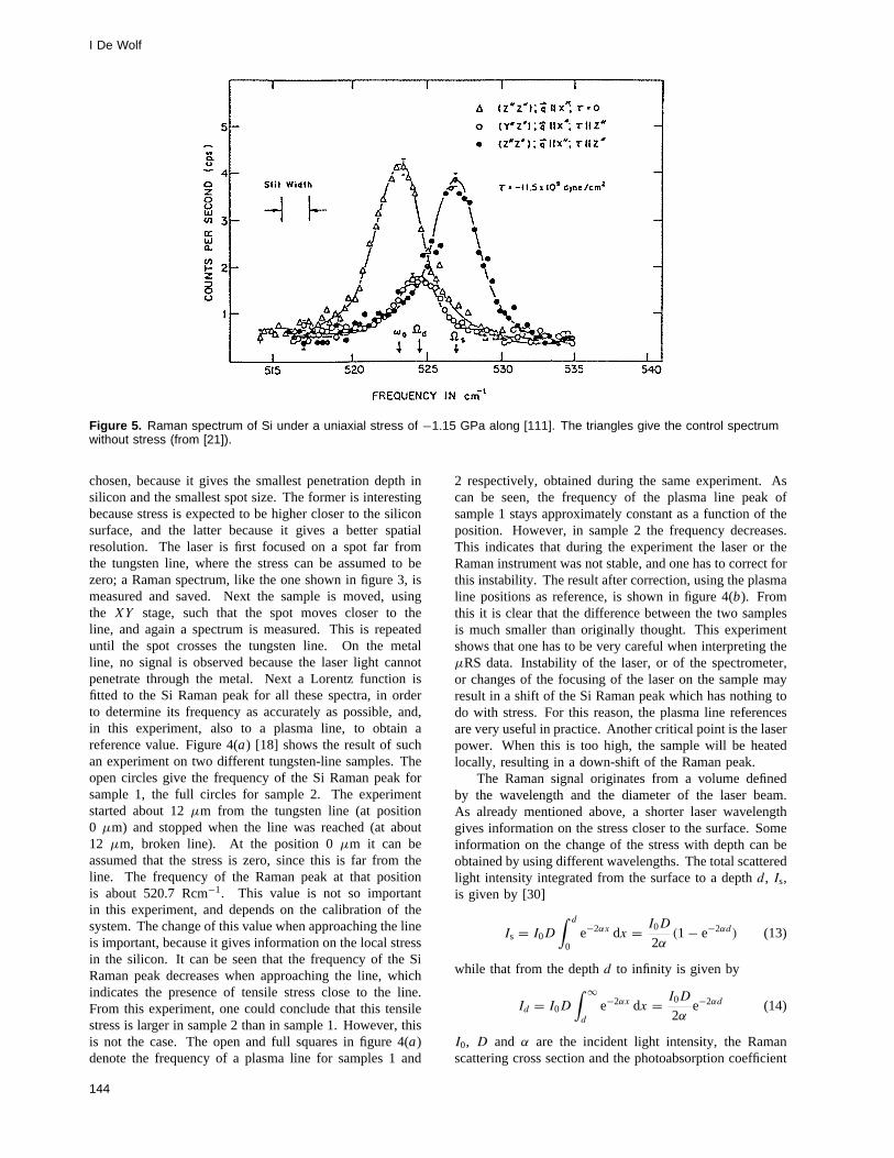
Figure 5. Raman spectrum of Si under a uniaxial stress of −1.15 GPa along [111]. The triangles give the control spectrumwithout stress (from [21]).
chosen, because it gives the smallest penetration depth insilicon and the smallest spot size. The former is interestingbecause stress is expected to be higher closer to the siliconsurface, and the latter because it gives a better spatialresolution. The laser is first focused on a spot far fromthe tungsten line, where the stress can be assumed to bezero; a Raman spectrum, like the one shown in figure 3, ismeasured and saved. Next the sample is moved, usingthe XY stage, such that the spot moves closer to theline, and again a spectrum is measured. This is repeateduntil the spot crosses the tungsten line. On the metalline, no signal is observed because the laser light cannotpenetrate through the metal. Next a Lorentz function isfitted to the Si Raman peak for all these spectra, in orderto determine its frequency as accurately as possible, and,in this experiment, also to a plasma line, to obtain areference value. Figure 4(a) [18] shows the result of suchan experiment on two different tungsten-line samples. Theopen circles give the frequency of the Si Raman peak forsample 1, the full circles for sample 2. The experimentstarted about 12µm from the tungsten line (at position0 µm) and stopped when the line was reached (at about12 µm, broken line). At the position 0µm it can beassumed that the stress is zero, since this is far from theline. The frequency of the Raman peak at that positionis about 520.7 Rcm−1. This value is not so importantin this experiment, and depends on the calibration of thesystem. The change of this value when approaching the lineis important, because it gives information on the local stressin the silicon. It can be seen that the frequency of the SiRaman peak decreases when approaching the line, whichindicates the presence of tensile stress close to the line.From this experiment, one could conclude that this tensilestress is larger in sample 2 than in sample 1. However, thisis not the case. The open and full squares in figure 4(a)denote the frequency of a plasma line for samples 1 and
2 respectively, obtained during the same experiment. Ascan be seen, the frequency of the plasma line peak ofsample 1 stays approximately constant as a function of theposition. However, in sample 2 the frequency decreases.This indicates that during the experiment the laser or theRaman instrument was not stable, and one has to correct forthis instability. The result after correction, using the plasmaline positions as reference, is shown in figure 4(b). Fromthis it is clear that the difference between the two samplesis much smaller than originally thought. This experimentshows that one has to be very careful when interpreting theµRS data. Instability of the laser, or of the spectrometer,or changes of the focusing of the laser on the sample mayresult in a shift of the Si Raman peak which has nothing todo with stress. For this reason, the plasma line referencesare very useful in practice. Another critical point is the laserpower. When this is too high, the sample will be heatedlocally, resulting in a down-shift of the Raman peak.
The Raman signal originates from a volume definedby the wavelength and the diameter of the laser beam.As already mentioned above, a shorter laser wavelengthgives information on the stress closer to the surface. Someinformation on the change of the stress with depth can beobtained by using different wavelengths. The total scatteredlight intensity integrated from the surface to a depthd, Is,is given by [30]
Is = I0D
∫ d
0e−2αx dx = I0D
2α(1 − e−2αd) (13)
while that from the depthd to infinity is given by
Id = I0D
∫ ∞
d
e−2αx dx = I0D
2αe−2αd (14)
I0, D and α are the incident light intensity, the Ramanscattering cross section and the photoabsorption coefficient
144

Local mechanical stress in silicon ICs
Table 2. Absorption coefficient (α) and penetration depth(dp) in crystalline silicon for different wavelengths (λ) of theargon laser.
λ (nm) λ (eV) 10−3α (cm−1) dp (nm)
514.5 2.410 14.96 770488.0 2.541 20.18 570457.9 2.708 36.43 320
of silicon respectively. If one assumes that the penetrationdepth,dp, is given by the depth that satisfies the relationshipId/(Is + Id) = 0.1, then this depth is given by
dp = − ln 0.1
2α= 2.3
2α. (15)
The absorption coefficient of silicon for the 514.5 nm(2.41 eV), 488 nm (2.54 eV) and 457.9 nm (2.71 eV)wavelength of the argon laser is obtained, using a third-degree interpolation, from [31] and, using equation (15),the penetration depth in crystalline silicon is found to be770 nm, 570 nm and 320 nm respectively. These resultsare summarized in table 2.
The relation between the measured Raman shift, asfor example shown in figure 4 for the tungsten line,and the mechanical stress present in the sample is notstraightforward. If one can assume that the stress in thesample is uniaxial or biaxial, the relation between Ramanshift and stress is simply linear (equations (10)–(12)).Although this assumption is usually wrong, it is often usedfor a first rough estimation of the magnitude of the stress inthe sample. If more detailed information on the magnitudeof the different stress components is required, it is necessaryto adapt a model describing the stress distribution in thesample, and to fit this model, using equation (8), to theRaman data. This was done for example in [18, 32–34].
3. Effect of externally applied forces on theRaman modes
Raman scattering measurements in the presence ofexternally applied stress have been performed by a largenumber of investigators on different kinds of samples. Themain underlying objectives of these studies were to obtaininsight in various aspects of lattice vibrational modes. Thefirst experimental investigation of the effect of externalstress on the Si Raman modes was done by Anastassakiset al [21]. The experiments were carried out in backscattering, with a 25 mW He–Ne laser (632.8 nm) asexcitation source, on rectangular Si samples(2 cm×1 mm×1 mm). Negative uniaxial stress was applied along thelong axis of the sample for two orientations of this axis,either [001] or [111]. For a uniaxial stress,σ , appliedalong either the [001] or the [111] direction, it can becalculated from equation (8) that the threefold degeneracyof the optical phonons of silicon is split into a singlet(ω3 = �s) with eigenvector parallel to the stress and adoublet (ω1 = ω2 = �d) with eigenvectors perpendicularto the stress. For observation of the splitting of the opticalphonons, the polarization selection rules were used [28,
Figure 6. Frequency shift of the singlet and doublet Ramancomponents measured as a function of the uniaxial stressalong [111]. The broken line shows the calculated shiftcorresponding to the hydrostatic component (from [35]).
equation (6)]. The polarization of the incident light wasswitched back and forth such that either the singlet or thedoublet could be observed. Typical spectra for the case ofuniaxial stress along [111] are shown in figure 5. In theabsence of stress, a single Raman peak is observed at afrequencyω0 of about 523 cm−1 (triangles). An externallyapplied compressive stress of−11.5×10⁹ dyn cm−2 resultsin a splitting into the singlet (full circles) and the doublet(open circles), and both are shifted towards higher Ramanfrequencies. From the slope of the shift of the frequencyof these peaks as a function of the applied stress, as shownin figure 6, values forp, q, r and for the mode Gruneisenparameterγ (= −∂ ln ω0/∂ ln V , where V is the volumeof the crystal) can be calculated. Figure 6 was takenfrom a later work of Anastassakiset al [35], where similarexperiments as in [21] were repeated, but this time usinga laser frequency in the region of transparency of silicon(Nd-YAG laser, 1.165 eV). This was necessary becauseseveral previous studies, for example on GaAs and InP (seereferences in [35]), showed that there is some relaxationof the stress near the surface, so that the phonon shiftsmeasured in the bulk may differ by 10 to 30% from thoseobserved near the surface. These experiments resultedin values for the phonon deformation potentialsp/ω2
0 =−1.85±0.06, q/ω2
0 = −2.31±0.06, r/ω20 = −0.71±0.02
and the Gruneisen parameterγ = 1.08± 0.06, which aresomewhat larger than the ones obtained in [21],p/ω2
0 =−1.25, q/ω2
0 = −1.87, r/ω20 = −0.66 andγ = 0.92, but
which are in closer agreement with theory [35].In later papers from the same group, calculations of the
effects of external stresses and strains (uniaxial, biaxial,as well as bisotropic [36]) on the Raman spectrum ofoptical phonons of different materials (Si, Ge, GaAs,GaSb, InAs, ZnSe, diamond, heterostructures) as wellas experimental results were presented and extensivelydiscussed [21, 22, 35–44].
4. Stress in silicon integrated circuits
4.1. Stress in SOI films
One of the first fields where Raman spectroscopy proved itsusefulness as a stress measuring technique was in the SOS
145

I De Wolf
Figure 7. Raman spectrum of bulk silicon and silicon onsapphire (from [44]).
(silicon-on-sapphire) field. It is known that a large built-instress, of the order of 108–109 Pa exists in the silicon filmin SOS devices. Englertet al [45] compared the Ramanpeak, measured in back scattering from the (001) surfaceof the film, with the Raman signal from a stress-free bulkreference wafer. The result is shown in figure 7. Thepeak obtained on SOS is up-shifted by1ω = 2.8 cm−1.The relation between Raman shift and stress was calculatedassuming biaxial compressive stress in the filmσxx = σyy =σ , (x = [100], y = [010]) and is given by equation (12).It was concluded that the stress in the SOS film was700 MPa. A shift of 2.8 cm−1 is very large, and can easilybe observed with all Raman spectroscopy instruments. Ingeneral, stress in Si semiconductor devices is smaller, andvery dedicated Raman instruments are necessary to observeit. The first paper on Raman spectroscopy on SOS filmswas followed by a large number of publications discussingthe annealing process of SOS films [46–50]. Later, micro-Raman spectroscopy results were also published, showingthe local variation of the stress in SOS device structures[51].
Silicon-on-insulator (SOI) films have been studiedextensively by Raman spectroscopy, not only to study thestress in these films but also the crystallinity and the effectof annealing [52–60]. The stress was measured near theseed/SOI boundary in a laser-recrystallized, seeded SOIfilm [52] and it was found that this stress increases overa distance of about 20µm from the seed/SOI boundary.Campbellet al [53] studied changes in crystallinity, stressand homogeneity on thin films of SOI irradiated by a singlelaser pulse. Raman spectroscopy was also often used tostudy the effect of implantation temperature [54] and lampor furnace annealing [54–56] on SIMOX (separation byimplantation of oxygen). Further, there were reports onthe dependence of the stress in laser-recrystallized SOIon the substrate, and on the insulator material used [57];on the stress in the top silicon film of an SOI structurerecrystallized by a graphite strip heater or an argon laser[58]; on the variation of this stress in depth [59] and onthe influence of a local buried insulating layer on the stressin the top silicon layer at the boundary region between thelocal SOI and the unimplanted region [60].
A difficulty that arises in some of these studies isthat the crystallinity may also affect the position of theRaman peak. It is therefore not always straightforwardin this kind of experiment to distinguish between botheffects. However, Raman spectroscopy proved to be a veryuseful technique to study these films. It provides not onlyinformation on the stress, but also on crystal quality of theSOI film.
4.2. Isolation
4.2.1. Local oxidation: LOCOS, PBLOCOS. The localoxidation of silicon (LOCOS) technique [61] is widely usedas an effective and relatively simple isolation techniquefor silicon integrated circuits. In this technique, Si3N4 isused as a mask against oxidation of the areas where theactive device will be formed. The different steps involvedin LOCOS isolation are as follows. In the first step, athin layer of SiO2, the pad oxide (PO), is grown on thesubstrate. On top of this a Si3N4 film is deposited andpatterned. This defines the oxidation mask. Next thewafer is subjected to a thermal oxidation process, givingrise to the field oxide (FO). However, since oxidation ofsilicon also takes place laterally, through the pad oxide,the growing oxide penetrates under the edges of the nitridemask, lifting them up. This gives rise to the formationof a specific geometrical feature, the so-called bird’s beak(BB). An undesired result of this is that the active areaof the device becomes smaller than the size of the initialnitride mask. At the end of the process the nitride film isremoved and the wafer is planarized.
There are some technological problems which ariseduring the application of LOCOS technology, and it wasvery soon understood that mechanical stress plays animportant role in them. For this reason, large efforts havebeen made to obtain information on this stress, and itsdependence on processing parameters.
Micro-Raman spectroscopy has proved to be a veryinteresting technique for the study of local mechanicalstress in LOCOS structures, and the effect of processingparameters on this stress. Kobayashiet al [62, 63] studiedthe stress in the active area of LOCOS samples afterthe nitride film and the pad oxide were removed. Theyperformed µRS experiments on samples with differentwidths,w, of the active area (from 9.2 to 1.2µm). Figure 8shows the shift of the Raman frequency from the zero-stress value as a function of the position on the sample.It was found that there is tensile stress (negative shift) inthe isolation area with a maximum at the field edges, andcompressive stress (positive shift) within the active areawith a maximum at the active area edges. Furthermore,they showed that this compressive stress in the active areaincreases with decreasing width. They compared theirexperiments with theoretical simulations, using a thermalstress model and assuming a linear relation between Ramanshift and stress. A similar study was reported by Brunneret al [64]; however, they focused on stress in the siliconsubstrate under the field oxide. Planar as well as cross-sectional data were reported.
From the point of view of dislocation formation, thestress before and after field oxidation, with the nitride
146

Local mechanical stress in silicon ICs
Figure 8. Raman frequency shift from stress-free value forLOCOS structures (after removal of the nitride film) withvarious active area widths (w ). Excitation source: 488 nmline of argon laser (from [62]).
mask still present, is of more importance. In particularthe stress at the tip of the BB is an important sourceof dislocation generation [1]. The variation of the stressin LOCOS and alternative LOCOS structures during thedifferent processing steps was studied byµRS in [32, 65–67]. Alternative isolation schemes, such as PBLOCOS(poly-buffered LOCOS), were introduced to reduce the fieldoxide encroachment under the nitride mask. PBLOCOSutilizes an Si3N4/poly-Si/SiO2 sandwich to block the fieldoxidation in the active regions. The formation of theBB is limited by the poly-Si film, and its presence alsoabsorbs stress from the nitride, allowing the pad oxide tobe thinned and the nitride to be thickened, to minimizethe BB. Figures 9–11 show the evolution of the localstress in PBLOCOS during three subsequent processingsteps: before field oxidation, after field oxidation, and afterremoval of the nitride mask. Figure 9 shows the resultof a µRS scan across a 10µm wide line of a PBLOCOSsample that was taken out of the processing before fieldoxidation. The 457.9 nm line of the argon laser was usedfor excitation of the spectra. The difference,1ω, betweenthe measured frequency of the silicon Raman peak and thestress-free value is plotted as a function of the positionacross the sample (open circles). The schematic drawingon top of the figure can be used to make a direct correlationbetween the measured Raman frequency and the positionon the structure where the signal is obtained. It can be seenin the figure that, upon approaching the line,1ω becomesnegative. This indicates tensile stress in the silicon justoutside the mask. Under the Si3N4 mask, 1ω becomespositive, indicating compressive stress. This experimentwas repeated for different thicknesses of the nitride film and
Figure 9. Raman frequency shift from stress-free value fora long 240 nm Si3N4/50 nm poly-Si/10 nm PO line, width9.4 µm, as shown at the top of the figure. Opencircles, experiment; full line, fit of the edge-force model tothe experiment. Exciting wavelength 457.9 nm (from [32]).
the pad oxide, and for different widths of the line [66, 67].In order to relate the measured Raman shift with mechanicalstress present in the sample, the secular equation has to besolved. This was done for this experiment [32], assumingthat the stress in the substrate, due to the line, could bedescribed by the simple analytical edge-force model of Hu[15]. In this model, it is assumed that this stress can bedescribed by edge forces,f , as indicated in figure 9. Thestrain tensor components were calculated, using this model,at different positions and at different depths in the substrate.Next the secular equation (equation (8)) was solved for allthese positions, and the Raman shift was calculated, takinginto account the penetration depth of the laser light and thedimensions of the beam spot. The result of the fit of thismodel to the data is given by the full curve in figure 9.Although the fit was found not to be so good for smallerlines (2.5µm), it could be concluded that this simple modelis already adequate to describe the stress in the silicon forthese structures.
After field oxidation, the stress picture changesdrastically. This is shown in figure 10, where the Ramanshift 1ω, measured before and after field oxidation, isplotted as a function of the position on the sample [66].A schematic drawing of the sample is shown on top ofthe figure. After field oxidation,1ω becomes negativeat the tip of the bird’s beak, indicating that tensile stressis present in the underlying substrate at that point. Insamples with thinner field oxides, this downward shift isobserved to be much larger [65, 67]. Further,1ω underthe nitride line is larger after FO than before FO. Thisis due to compressive stress exerted by the FO on theactive area. Because of the volume expansion duringoxidation of silicon and because of the difference in thermalexpansion coefficients of SiO2 and Si, the silicon regionslying between the FO regions will be compressed by the
147

I De Wolf
Figure 10. Raman frequency shift from the stress-freevalue for a PBLOCOS sample with 10 nm PO, 50 nmpoly-Si and 150 nm Si3N4, before field oxidation (opencircles) and after field oxidation at 950 ◦C (full circles). Thevertical lines denote the borders of the 5 µm wide nitridefilm. The sample after FO is shown schematically at thetop. Exciting wavelength 457.9 nm (from [65]).
latter. This compressive stress acts also at the bird’s beaktip. So, at that position there is a combination of tensilestress, mainly in the vertical direction, and compressivestress, mainly acting horizontally. Also the bent nitridefilm edge will introduce compressive stress in the silicon.The frequency of the silicon Raman peak is influenced byall the stress components.
The main effect of removal of the nitride mask and theunderlying poly-Si film is a relaxation of the tensile stressregion at the bird’s beak. As can be seen in figure 11,the negative shift of1ω at the bird’s beak tip completelydisappears, and the only forces which are still present arethe compressive forces from the FO.
Similar studies were performed on samples withdifferent thicknesses of the pad oxide, the field oxide andthe Si3N4. Also stress surrounding LOCOS structures onSIMOX wafers was studied, and it was found that the stressin the Si film is highly influenced by the field oxidation time[68]. It was also shown that the tensile stress at the bird’sbeak tip is much larger in PBLOCOS structures than inLOCOS structures, and that, in general, a reduction of thebird’s beak length gives rise to an increase in stress. As aresult, the risk for defect generation will also increase.
Although extraction of stress values from the Ramanexperiments was done in these studies only for the simpleline structures (figure 9), the experiments did provideinformation on the origin of the stress, the sign of the stress,and the influence of processing steps on the magnitudeand on the stress distribution. Joneset al [33] wentone step further, they used finite element modelling tocalculate the field oxidation induced stress in the substrateof PBLOCOS structures, and using these results, theycalculated the corresponding Raman shift. They obtaineda good agreement between the model and the experimental
Figure 11. Raman frequency shift from the stress-freevalue for a sample with 14 nm PO, 50 nm poly-Si, 150 nmSi3N4 and 900 nm FO grown at 950 ◦C before (full symbols)and after (open symbols) removal of the Si3N4 and poly-Sifilm by dry etching. The vertical lines indicate the bordersof the 5 µm wide nitride film. The sample after the strip isshown at the top. Exciting wavelength 457.9 nm (from [65]).
results. A very interesting experiment on PBLOCOSstructures, after field oxidation, is shown in figure 12 [69].In this experiment aµRS scan was performed across arraysof PBLOCOS stripe structures (six stripes per array) withwidths varying from 4µm down to 0.35µm. ‘O’ denotesthe position of the FO, ‘N’ denotes the position of thenitride line. The finite resolution of the Raman probe causesincreased blurring of the stress variations below the 1µmgeometry, but it can clearly be seen that the average stressbecomes increasingly tensile for smaller lines, until a stressrelaxation occurs at the 0.5µm PBLOCOS stripes andbelow. The cause of this relaxation was revealed by XTEMpictures: the nitride mask was found to be completelylifted for the lines with width≤ 0.5 µm, because forthese dimensions the 0.25µm long bird’s beaks completelyencroach the active area. These results indicated that afurther down scaling of the devices will be difficult usingPBLOCOS isolation.
4.2.2. Trenches. The drive for increased density inintegrated circuits has led to ‘trench technology’, whichinvolves anisotropic etching of patterns into the substrateto form trenches, and subsequently filling them withSiO2 or poly-Si. These trenches are used as storagecapacitors in dynamic memory (DRAM) technologies (deepstorage trenches), or as isolation structures in CMOS,bipolar and BiCMOS technologies. As discussed above,LOCOS cannot be scaled down much further, and shallowtrenches offer an attractive solution. Although trenchesare advantageous from a density point of view, trenchstructures have been shown to be a major contributing factorin substrate defect generation during the processing [70–76]. The defect generation is directly related to mechanical
148

Local mechanical stress in silicon ICs
Figure 12. Raman scan across an array of PBLOCOS structures with geometry varying from 4 µm down to 0.35 µmprocessed with 10 nm PO, 50 nm poly-Si, 150 nm nitride and 600 nm FO grown at 975 ◦C. Exciting wavelength 457.9 nm(from [68]).
stress surrounding the trench, and for this reason a growingbody of literature is devoted to the study of this stress,mostly by theoretical calculations (analytical models andfinite element calculations), and to the effect of processingconditions (oxidation, deposition, annealing) and of trenchgeometry on the stress magnitude [20, 72–81].
One of the first attempts to analyse the stress arounddeep trenches, filled with poly-Si or SiO2, experimentally,was done by Nadaharaet al [81]. The Raman shift wasmeasured at different depths in between two trenches, ona cleaved sample. Although the Raman shift was onlystudied at three points, and although it was assumed thatthe stress could be calculated from the Raman shift usingequation (11), which is only valid for uniaxial stress,the results were very promising. There was a goodcorrelation between the results and the predictions fromFE simulations. Furthermore, the authors showed thatinformation about the variation of the stress with depth canbe obtained by measuring on a cleaved sample.
Nowadays,µRS is often used to control mechanicalstress around trench isolation in order to optimize theisolation structure with regard to stress [74–76, 82, 83].An interesting paper comparing stress surrounding acombination of shallow and deep trench structures for threedifferent processes was published by Itohet al [76]. Thethree processes are described in figure 13(a). The stressmeasured by Raman spectroscopy for the three processesis shown in figure 13(b). Here also the stress values werecalculated from the Raman shift assuming uniaxial stress(equation (11)). The stress in processes A and C wasfound to be high, while in process B it was low. Thiswas explained by temperature differences between the threeprocesses: in B, the filling occurred at a low temperature.
Deep trenches in combination with LOCOS isolationare commonly used in bipolar transistors. These devicesoften show high leakage current and low yield, which isattributed to stress-induced defects. That the combination
of deep trenches and LOCOS gives rise to large stressvariations is shown in figure 14 [83], where the result ofa µRS scan across the first bipolar device of an array isshown. The experiment was performed on devices from abulk 1.25µm BiCMOS process, which were taken out ofthe processing just after LOCOS oxidation. The trenches(1.5 µm wide, 8µm deep) had an SiO2 sidewall liner andwere filled with LPCVD poly-Si. At both collector window(CW) and base-emitter window (BEW) a distorted imageof the stress in an isolated LOCOS (see figure 8) is found.At the trench edges, a large upward shift of the Si Ramanpeak is observed. Assuming uniaxial stress, this shift wouldindicate a compressive stress of about−370 MPa. Thestress outside the array (at−5 µm) becomes zero, while inbetween two devices (at 25µm) it remains compressive.µRS experiments were also performed at different depthson a cleaved sample. The stress was found to be tensileat the trench border deeper in the substrate and in thepoly-Si, and compressive closer to the surface and at theBEW and CW. TheµRS data of planar and cross-sectionalexperiments were found to correlate very well, and theobserved variations in stress correspond with variationspredicted by simulations [80].
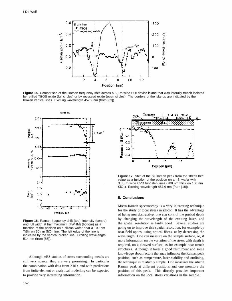
µRS was also used to study and compare process-induced mechanical stresses in recessed oxide-isolated andTEOS refilled trench-isolated SOI device islands [84].Figure 15 shows the result of a scan across a 5µmwide island. The right-hand axis gives the stress valuescalculated from the Raman shift, assuming uniaxial stress.The edges of the islands are indicated by the verticalbroken lines. The experiments show that the SOI islandsisolated by recessed oxide are under high compressivestress. Tensile stress is observed at the edges. On theother hand, the islands isolated by TEOS oxide refilledtrenches show practically no stress, except for the edgeswhere tensile stress is also observed.
149

I De Wolf
Figure 13. (a) Trench isolation structure and fabrication flow for three processes (from [75]). (b) Mechanical stressdistribution maps for the three isolation structures as measured by Raman spectroscopy. Exciting wavelength 457.9 nm(from [75]).
4.3. Metal structures
One of the important issues of concern for submicrometreintegrated circuit technology is the large mechanical stressin metal interconnect lines. These stresses are one of theimportant driving forces for electromigration-induced voidformation and growth. They can even be large enough tocause immediate failure of the lines. Stresses in metalsare in general measured by XRD. The disadvantage of thistechnique is the large probed area and the large penetrationdepth of the x-rays. As a result, only information about themean value of the stress components in the metal structurescan be obtained.µRS has a better spatial resolution anda smaller penetration depth than XRD, but no Ramansignal can be obtained from the metal. However,µRScan be used to provide information on the stress in the Sisubstrate adjacent to the metal structures. This information
is important as such, but it can also be used to give feedbackto theoretical models and for comparison with the XRDresults.
Sakataet al [85] usedµRS to study stress in siliconnear tungsten lines. A Raman spectrum was measuredat three points near the lines, separated by 0.1µm.The measurements were performed using two polarizationdirections: the incident light was polarized either alongthe width or along the length of the lines. They used the514 nm argon laser line. The laser spot size was about1 µm, but when the spot partly probes the metal, the areaactually probed is smaller. The authors did correct for thiseffect by taking the differential spectrum from two spectraobtained at adjacent points, including the effect of laserpower. They found that the Si Raman peak shifted towardshigher frequencies near the line, indicating compressive
150

Local mechanical stress in silicon ICs
Figure 14. Raman frequency shift across the first device ofan array of bipolar structures, taken out of the processingafter field oxidation. T1 and T2 denote the trenches, BEWis the base-emitter window and CW is the collector window.The 8 µm deep trenches are filled with poly-Si. Excitingwavelength 457.9 nm (experiment from [82]).
stress. In order to calculate the stress, uniaxial stress wasassumed.
It can be noted that the penetration depth of the 514 nmline, used in these experiments, is rather large (see table 2).The stress is expected to be larger closer to the surface,and for this reason it is more interesting to use the shorter457.9 nm laser line of the argon laser for this kind ofexperiment, if available. Two additional advantages ofusing this line are that the spot size is somewhat smallerthan the spot size of the 514 nm line, and that the plasmalines can be used as reference. Indeed, for the 514 nm linethere is a plasma line located exactly at the position of theSi Raman peak, at 520 Rcm−1; it is therefore necessaryto use filters or a monochromator to get rid of this line.The plasma lines for the 457.9 nm line, however, do notinterfere with the Si Raman line.
Close to the edge of a metal line, the assumption of‘uniaxial stress’ is certainly not valid, and more modellingis required to obtain quantitative information on the stresscomponents from the measured Raman shift. A first stepin that direction was made by Graf [86], who studiedstress in the silicon substrate near TiSi2 films of differentthicknesses. A typical result of these experiments is shownin figure 16, for a 100 nm thick TiSi2 film on 500 nm SiO2
on silicon. The Raman frequency (top), intensity (centre)and full width at half maximum (bottom) are shown as afunction of the position on the sample. The left edge of theline is indicated by the vertical broken line. Also for theseexperiments, the 514 nm line of the laser was used. Thespot size was estimated, from the change of the intensityof the Si signal when crossing the silicide film, to be about1 µm. A negative shift of the Raman frequency was foundnear the film edge, indicating tensile stress. This shift wasshown to increase with increasing thickness of the film,from 0.03 cm−1 for the 30 nm film to 0.18 cm−1 for the100 nm film. Graf compared the results with a concentrated
edge force model, similar to the one of Hu [15], and usedthis model to calculate, using equation (8), the expectedRaman shift for different depths in the substrate, for thethree Raman modes. A special program was written forthese calculations. The model predicts a negative shift ofthe frequency of the Raman line close to the metal line,as was observed in the experiments. However, a fit of themodel to the experiments was not done.
More accurate information on stress in and near metallines, obtained by combining theoretical models withRaman data, was obtained by Maet al [34] and De Wolfet al [18]. Ma et al used µRS to study stress nearpassivated aluminium lines, and compared the results withfinite element calculations. They assumed a very smallabsorption depth of the probing laser line (514 nm) of200 nm, and therefore only the stresses calculated withfinite elements at the top row of points in the meshwere taken into account for the Raman shift calculation.They corrected for the probe size of the laser by takinga convolution of the calculated stress variation and theGaussian intensity profile of the laser beam. The beam spotdiameter was experimentally determined to be about 1µm,but a size of 1.5µm was used to fit the calculations to theRaman data. It was concluded from these experiments thatthe Raman shift in the silicon near the Al lines is principallydependent on the hydrostatic stress in the interconnect.This stress therefore probably provides the driving forcefor voiding. They also studied the stress variations inthe silicon substrate along two Al lines, a control lineand a electromigration-tested line. Uniform stresses werefound along the line for the as-fabricated sample, whilestress variations were found for the electromigration-testedsample.
The penetration depth of 200 nm for the 514 nm laserline, as used in this study, is probably an underestimation(see table 2). As a result, the stress values used to fit themodel to the data were too high. This may explain thediscrepancy between the measured spot diameter and thefitted spot diameter. Indeed, using a larger spot size willresult in a reduction of the measured variations in stress.
µRS, XRD and analytical modelling were used in [18]to study stresses in and surrounding highly tensile tungstenlines of two different widths and spacing. The stress inthe lines and in the adjacent substrate was calculated usingtwo analytical models: a concentrated and a distributededge force model, and using finite element calculations.The values obtained for the stress in the lines and inthe substrate, using the results from these models, werecompared with the experimental results from XRD andµRS, and a very good agreement was found. Figure 17shows the result of a scan across the first and the secondtungsten line of the wide-line array. The Raman shiftobtained far from the lines was taken as the stress-freereference value (0 Rcm−1 in the figure). Upon approachingthe first line, the Raman frequency shifts downwards,indicating tensile stress. Under the line, no Raman signalcan be obtained because the laser light cannot penetrate themetal. In between the lines, a downward shift is measured,with maximum near the edges of the lines, and minimumat the centre (c) in between the lines.
151
I De Wolf
Figure 15. Comparison of the Raman frequency shift across a 5 µm wide SOI device island that was laterally trench isolatedby refilled TEOS oxide (full circles) or by recessed oxide (open circles). The borders of the islands are indicated by thebroken vertical lines. Exciting wavelength 457.9 nm (from [83]).
Figure 16. Raman frequency shift (top), intensity (centre)and full width at half maximum (FWHM) (bottom) as afunction of the position on a silicon wafer near a 100 nmTiSi2 on 60 nm SiO2 line. The left edge of the line isindicated by the vertical broken line. Exciting wavelength514 nm (from [85]).
Although µRS studies of stress surrounding metals arestill very scarce, they are very promising. In particularthe combination with data from XRD, and with predictionsfrom finite element or analytical modelling can be expectedto provide very interesting information.
Figure 17. Shift of the Si Raman peak from the stress-freevalue as a function of the position on an Si wafer with3.8 µm wide CVD tungsten lines (700 nm thick on 100 nmSiO2). Exciting wavelength 457.9 nm (from [18]).
5. Conclusions
Micro-Raman spectroscopy is a very interesting techniquefor the study of local stress in silicon. It has the advantageof being non-destructive, one can control the probed depthby changing the wavelength of the exciting laser, andthe spatial resolution is fairly good. Several studies aregoing on to improve this spatial resolution, for example bynear-field optics, using optical fibres, or by decreasing thewavelength. One can measure on the sample surface, or, ifmore information on the variation of the stress with depth isrequired, on a cleaved surface, as for example near trenchstructures. Although it takes a good instrument and someknowledge about factors that may influence the Raman peakposition, such as temperature, laser stability and outlining,the technique is relatively simple. One measures the siliconRaman peak at different positions and one monitors theposition of this peak. This directly provides importantinformation on the local stress variations in the sample.
152

Local mechanical stress in silicon ICs
When one wants to compare stress due to differentmaterials or in samples with different geometry, it is notreally necessary to use extensive calculations to correlatethe Raman shift with the stress. Although the assumption‘uniaxial stress’ is not always correct, it can be usedto provide a first indication on the sign and magnitudeof the stress, and on differences in local stress betweendifferent investigated structures. For example, in the above-discussed study on stress near tungsten lines [18], it couldbe concluded immediately from the Raman experiments thatthe stress surrounding the narrow tungsten lines is smallerthan the stress surrounding the wide tungsten lines, andfrom this it could be predicted that the stress in the narrowlines must be smaller than the stress in the wide lines, whichcorresponds with XRD observations.
It is in general not so easy to obtain information onthe different stress tensor components from the Ramanspectroscopy measurements. New techniques, such aspolarized off-axis Raman spectroscopy [87], are underdevelopment and promise to give more information on thestress tensor. Also, comparison of the Raman shift withpredictions by models describing the stress is possible. Inthat case, the measured Raman shift should be comparedwith the Raman shift predicted by these models, includingeffects of penetration depth, probing spot diameter andeffects of scanning across edges of films (i.e. metals) onthis spot size. This is elaborate work, involving a lot ofcomputer calculations, but, as some of the above-discussedreports show, it is certainly worth the effort.
Acknowledgments
I would like to thank E Anastassakis, whose extensivework on the effects of mechanical stress on Ramanfrequency modes introduced me to the subject, and wasindispensable for my work. Further, I would like tothank all my colleagues at IMEC and at other places whoprovided me with a lot of interesting samples and withwhom I have enjoyed many fruitful stimulating discussions:Hans Norstrom, Jan Vanhellemont, Albert Romano, RitaRooyackers, Ludo Deferm, Guido Groeseneken, HerbertMunder, Pepe Menendez, Kevin Yallup, Helmut Baumgart,Ann Witvrouw, Karen Maex, Steven Jones, Edouard DaSilva and Michel Ignat. In particular I would like to thankHerman E Maes who suggested this subject to me as aninteresting research topic and who supported it. This workwas partly supported by a NATO Collaborative ResearchGrant, CRG 940198.
References
[1] Hu S M 1991J. Appl. Phys.70 R53–R79[2] Itoh M, Inoue N, Hirashita N and Yoshimaru M 1992
Extended Abstracts of the 1992 Int. Conf. on Solid StateDevices and Materials (SSDM) (Tsukuba, Japan)pp 428–30
[3] Park H, Jones K S, Slinkman J A and Law M E 1993Proc.1993 Int. Electron Devices Meeting (IEDM)pp 303–6
[4] Hamada A, Furasawa T, Saito N and Takeda E 1992Semicond. Sci. Technol.7 B593–6
[5] Degraeve R, De Wolf I, Groeseneken G and Maes H E1994Proc. 1994 IEEE Int. Reliability Physics Symp.(IRPS)(New York: IEEE) pp 29–33
[6] Flinn P A and Waychunas G A 1988J. Vac. Sci. Technol.B6 1749–55
[7] Greenebaum B, Sauter A I, Flinn P A and Nix W D 1991Appl. Phys. Lett.58 1845–7
[8] Dehaven P and Goldsmith C 1993Mater. Res. Soc. Symp.Proc. 308 343–8
[9] Yamamoto N and Sakata S 1989Extended Abstracts of the1989 Int. Conf. on Solid State Devices and Materials(SSDM) (Tokyo, Japan)pp 221–4, C-2-2
[10] Armigliato A, Balboni R, De Wolf I, Frabboni S, JanssensK G F and Vanhellemont J 1993Inst. Phys. Conf. Ser.134 pp 229–34
[11] Kimoto K, Usami K, Sakata H and Tanaka M 1993Japan.J. Appl. Phys.32 L211–L213
[12] Gardner D S and Flinn P A 1990J. Appl. Phys.67 1831–44[13] Flinn P A 1989Mater. Res. Soc. Symp. Proc.130 41–51[14] Moske M, Ho P, Hu C K and Small M 1992Stress-Induced
Phenomena in Metallizationed C Li, P Totta and P Ho(New York: American Institute of Physics) p 195
[15] Hu S M 1979J. Appl. Phys.50 4661–6[16] Zeyfang R 1971Solid-State Electron.14 1035[17] Mezin A, Chambard J-P, Lepage J and Nivoit M 1990Thin
Solid Films185 57–69[18] De Wolf I, Maes H E, Moffet J, Ignat M 1995Mater. Res.
Soc. Symp. Proc.at press[19] Atkinson A, Johnson T, Harker A H and Jain S C 1995
Thin Solid Filmsat press[20] Hu S M 1990J. Appl. Phys.67 1092–101[21] Anastassakis E, Pinczuk A, Burstein E, Pollak F H and
Cardona M 1970Solid State Commun.8 133–8[22] Anastassakis E 1980Dynamical Properties of Solids
ed G K Horton and A A Maradudin, ch 3[23] Cardona M 1987Proc. SPIE822 2–15[24] Mooradian A 1969Festkorper Probleme IX, Advances in
Solid State Physicsed O Madelung (Marburg:Pergamon) pp 74–98
[25] Pollak F H 1985Test and Measurement WorldMay[26] Bruesch P 1981Phonons: Theory and Experiments.
Lattice Dynamics and Models of Interatomic Forces(Springer Series in Solid-State Sciences 34)(Berlin:Springer)
[27] Cardona M 1982Light Scattering in Solids II (Topics inApplied Physics 50)ed M Cardona and G Guntherodt(Berlin: Springer)
[28] Loudon R 1964Adv. Phys.13 423–80[29] Ganesan S, Maradudin A A and Oitmaa J 1970Ann. Phys.
56 556–94[30] Takahashi J-I and Makino T 1988J. Appl. Phys.63 87–91[31] Aspnes D E and Studna A A 1983Phys. Rev.B 27
985–1008[32] De Wolf I, Maes H E and Jones S K 1995J. Appl. Phys.at
press[33] Jones S K, Poncet A, De Wolf I, Ahmed M and Rothwell
W J 1994Proc. 1994 Int. Electron Devices Meeting(IEDM) pp 35.5.1–4
[34] Ma Q, Chiras S, Clarke D R and Suo Z 1995J. Appl. Phys.78 1614–22
[35] Anastassakis E, Cantarero A and Cardona M 1990Phys.Rev.B 41 7529–35
[36] Anastassakis E 1990J. Appl. Phys.68 4561–8[37] Anastassakis E 1985Physical Problems in Microelectronics
ed J Kassabov, p 128[38] Anastassakis E 1992Solid State Commun.84 47–50[39] Anastassakis E 1981J. Raman Spectrosc.10 64–76[40] Anastassakis E 1992Phys. Rev.B 46 4744–7[41] Anastassakis E and Burstein E 1971J. Phys. Chem. Solids
32 313–26[42] Anastassakis E and Burstein E 1971J. Phys. Chem. Solids
32 563–70
153

I De Wolf
[43] Buchenauer C J, Cerdeira F and Cardona M 1971Proc.2nd Int. Conf. on Light Scattering in SolidsedM Balkanski (Flammarion) pp 280–3
[44] Cerdeira F, Buchenauer C J, Pollak F H and Cardona M1972Phys. Rev.B 5 580–93
[45] Englert Th, Abstreiter G and Pontcharra J 1980Solid-StateElectron.23 31–3
[46] Sai-Halasz G A, Fang F F, Sedgwick T O and Segmuller A1980Appl. Phys. Lett.36 419–22
[47] Yamazaki K-I, Yamada M, Yamamoto K and Abe K 1981Japan. J. Appl. Phys.20 L299–L302
[48] Ohmura Y, Inoue T and Yoshii T 1981Solid StateCommun.37 583–5
[49] Yamazaki K-I, Yamada M, Yamamoto K and Abe K 1984Japan. J. Appl. Phys.23 681–6
[50] Nakamura M, Kobayashi Y and Usami K 1984Japan. J.Appl. Phys.23 687–94
[51] Brueck S R J, Tsaur B-Y, Fan J C C,Murphy D V,Deutsch T F and Silversmith D J 1982Appl. Phys. Lett.40 895–8
[52] Zorabedian P and Adar F 1983Appl. Phys. Lett.43 177–9[53] Campbell L H and Fauchet P M 1985Mater. Res. Soc.
Symp. Proc.53 311–16[54] Olego D J, Baumgart H and Celler G K 1988Appl. Phys.
Lett. 52 483–5[55] De Wolf I, Vanhellemont J and Maes H E 1990Mater. Res.
Symp. Proc.188 53–8[56] Perez A, Portillo J, Cornet A, Jimenez J, Morante J R,
Hemment P L F andHomewood K P 1991Nucl.Instrum. Methods Phys. Res.B 55 714–17
[57] Ogura A, Egami K and Kimura M 1985Japan. J. Appl.Phys.24 L669–L671
[58] Liu L, Chen P, Tsien P and Li Z 1988Electron. Lett.241420–2
[59] Kanamori M and Tsuya H 1988J. Electron. Mater.17 33–7[60] Kato K, Takai M, Namba S, Schork R and Ryssel H 1991
Nucl. Instrum. Methods Phys. Res.B 55 710–13[61] Appels J A, Kooi E, Paffen M M, Schatorge J J H and
Verkuylen W H C G 1970Philips Res. Rep.25 118[62] Kobayashi K, Inoue Y, Nishimura T, Nishioka T, Arima H,
Hirayama M and Matsukawa T 1987Extended Abstractsof the 19th Int. Conf. on Solid State Devices andMaterials (SSDM) (Tokyo, Japan)pp 323–6
[63] Kobayashi K, Inoue Y, Nishimura T, Hirayama M,Akasaka Y and Kato T 1990J. Electrochem. Soc.1371987–9
[64] K Brunner, Abstreiter G, Kolbesen B O and Meul H W1989Proc. Conf. on Insulating Films on Semiconductors(INFOS)ed F Koch and A Spitzen, p 116
[65] De Wolf I, Vanhellemont J, Romano-Rodrıguez A,Norstrom H and Maes H E 1992J. Appl. Phys.71898–906
[66] De Wolf I, Maes H E and Norstrom 1993Mater. Res. Soc.Symp. Proc.308 356–60
[67] De Wolf I, Norstrom H and Maes H E 1993J. Appl. Phys.74 4490–500
[68] De Wolf I, Vanhellemont J and Maes H E 1992Silicon-on-Insulator Technology and Devicesed W EBailey (Pennington, NJ: The Electrochemical Society)p 307
[69] Jones S K, Ahmed A, Rothwell W J, De Wolf I andDeferm L 1994Proc. 24th European Solid State DeviceResearch Conf. (ESSDERC)ed C Hill and P Ashburn(Paris: Editions Frontieres) pp 255–8
[70] Takano Y and Kozuka H 1983Proc. 14th Int. Conf. onSolid State Devices and Materials (SSDM) (Tokyo,Japan)(Japan. J. Appl. Phys.22 553–6)
[71] Takami Y, Isomae S, Sagara K and Kure T 1988J. Electrochem. Soc.135 726–30
[72] Stiffler S R, Lasky J B, Koburger C W and Berry W S1990 IEEE Trans. Electron Devices37 1253–8
[73] Isomae S and Aoki S 1986Extended Abstracts of the 18thInt. Conf. on Solid State Devices and Materials (SSDM)(Tokyo, Japan)pp 517–20
[74] Matsuda S, Yoshino C, Nakajima H, Inou K, Yoshitomi S,Katsumata Y and Iwai H 1994Proc. 1994 Int. ElectronDevices Meeting (IEDM)pp 885–8
[75] Katsumata Y, Katakabe I, Itoh N, Tsukioka E, Yoshino Cand Iwai H 1991IEEE 1991 Bipolar Circuits andTechnology Meeting 113pp 271–4
[76] Itoh N, Yoshino V C, Matsuda S, Tsuboi Y, Inou K,Katsumata K and Iwai H 1992IEEE 1992 BipolarCircuits and Technology Meeting 4.7pp 104–7
[77] Stiffler S R and Cifuentes A O 1993IEEE Trans. ElectronDevices40 557–63
[78] Vasquez B and Theodore N D 1992Mater. Res. Soc. Symp.Proc. 262 725–30
[79] Stiffler S R 1990J. Appl. Phys.68 351–5[80] Chidambarrao D, Peng J P and Srinivasan G R 1991
J. Appl. Phys.70 4816–22[81] Nadahara S, Kambayashi S, Watanabe M and Nakakubo T
1987Extended Abstracts 19th Int. Conf. on Solid StateDevices and Materials (SSDM) (Tokyo, Japan)pp 327–30
[82] Rothwell W J, Hill C and Pearson P J 1992Proc. 13th Int.Conf. on Raman Spectroscopy (ICORS 1992)edW Kiefer et al (New York: Wiley) pp 1064–5
[83] De Wolf I, Maes H E and Yallup K 1993Proc. 23rdEuropean Solid State Device Research Conf. (ESSDERC)ed J Borelet al (Paris: Editions Frontieres) pp 565–8
[84] Baumgart H, Letavic I I, De Wolf I, Maes H E and EgloffR 1995Proc. Electrochem. Soc. 3rd Int. Symp. on WaferBonding Science, Technology and Applications (SpringMeeting, May 1995)at press
[85] Sakata H, Hatsuda T and Kawai S 1990Proc. 4th Int.Conf. on Exp. Mech.3 1307–12
[86] Graf P 1990Diplomarbeit in PhysikMathematisch-Naturwissenschaftlichen Fakultat derRheinisch-Westfalischen Technushen Hochschule,Aachen (in German)
[87] Loechelt G H, Cave N G and Menendez J 1995Appl. Phys.Lett. 66 3639–41
154