
TMS320x280x, 2801x, 2804x System Control and … · TMS320x280x, 2801x, 2804x DSP System Control...
151
TMS320x280x, 2801x, 2804x DSP System Control and Interrupts Reference Guide Literature Number: SPRU712H November 2004 – Revised October 2012
Transcript of TMS320x280x, 2801x, 2804x System Control and … · TMS320x280x, 2801x, 2804x DSP System Control...

TMS320x280x, 2801x, 2804x DSPSystem Control and Interrupts
Reference Guide
Literature Number: SPRU712H
November 2004–Revised October 2012

Contents
Preface ....................................................................................................................................... 9
1 Memory ............................................................................................................................ 121.1 Flash and OTP Memory .................................................................................................. 13
1.1.1 Flash Memory ..................................................................................................... 131.1.2 OTP Memory ...................................................................................................... 13
1.2 Flash and OTP Power Modes ........................................................................................... 131.2.1 Flash and OTP Performance ................................................................................... 151.2.2 28x Flash Pipeline Mode ........................................................................................ 161.2.3 Reserved Locations Within Flash and OTP ................................................................... 171.2.4 Procedure to Change the Flash Configuration Registers ................................................... 17
1.3 Flash and OTP Registers ................................................................................................ 19
2 Code Security Module (CSM) .............................................................................................. 252.1 Functional Description .................................................................................................... 262.2 CSM Impact on Other On-Chip Resources ............................................................................ 282.3 Incorporating Code Security in User Applications ..................................................................... 28
2.3.1 Environments That Require Security Unlocking .............................................................. 292.3.2 Password Match Flow ........................................................................................... 312.3.3 Unsecuring Considerations for Devices With/Without Code Security ..................................... 32
2.4 Do's and Don'ts to Protect Security Logic .............................................................................. 342.4.1 Do's ................................................................................................................. 342.4.2 Don'ts .............................................................................................................. 34
2.5 CSM Features - Summary ............................................................................................... 34
3 Clocking ........................................................................................................................... 353.1 Clocking and System Control ............................................................................................ 363.2 OSC and PLL Block ....................................................................................................... 43
3.2.1 PLL-Based Clock Module ....................................................................................... 433.2.2 Main Oscillator Fail Detection ................................................................................... 443.2.3 XCLKOUT Generation ........................................................................................... 463.2.4 PLL Control (PLLCR) Register .................................................................................. 473.2.5 PLL Control, Status and XCLKOUT Register Descriptions ................................................. 483.2.6 External Reference Oscillator Clock Option .................................................................. 50
3.3 Low-Power Modes Block ................................................................................................. 503.4 Watchdog Block ........................................................................................................... 53
3.4.1 Servicing The Watchdog Timer ................................................................................. 543.4.2 Watchdog Reset or Watchdog Interrupt Mode ............................................................... 543.4.3 Watchdog Operation in Low Power Modes ................................................................... 553.4.4 Emulation Considerations ....................................................................................... 553.4.5 Watchdog Registers .............................................................................................. 56
3.5 32-Bit CPU Timers 0/1/2 .................................................................................................. 58
4 General-Purpose Input/Output (GPIO) .................................................................................. 634.1 GPIO Module Overview ................................................................................................... 644.2 Configuration Overview ................................................................................................... 654.3 Digital General Purpose I/O Control .................................................................................... 664.4 Input Qualification ......................................................................................................... 68
2 Contents SPRU712H–November 2004–Revised October 2012Submit Documentation Feedback
Copyright © 2004–2012, Texas Instruments Incorporated
www.ti.com
4.4.1 No synchronization (asynchronous input): .................................................................... 684.4.2 Synchronization to SYSCLKOUT only: ........................................................................ 684.4.3 Qualification using a sampling window: ....................................................................... 68
4.5 GPIO and Peripheral MUXing ........................................................................................... 724.6 Register Bit Definitions .................................................................................................... 83
5 Peripheral Frames ............................................................................................................ 1025.1 Peripheral Frame Registers ............................................................................................ 1035.2 EALLOW-Protected Registers .......................................................................................... 1045.3 Device Emulation Registers ............................................................................................ 1095.4 Write-Followed-by-Read Protection ................................................................................... 110
6 Peripheral Interrupt Expansion (PIE) .................................................................................. 1126.1 Overview of the PIE Controller ......................................................................................... 113
6.1.1 Interrupt Operation Sequence ................................................................................. 1136.2 Vector Table Mapping ................................................................................................... 1166.3 Interrupt Sources ......................................................................................................... 117
6.3.1 Procedure for Handling Multiplexed Interrupts .............................................................. 1196.3.2 Procedures for Enabling And Disabling Multiplexed Peripheral Interrupts .............................. 1206.3.3 Flow of a Multiplexed Interrupt Request From a Peripheral to the CPU ................................. 1216.3.4 The PIE Vector Table .......................................................................................... 122
6.4 PIE Configuration Registers ............................................................................................ 1336.5 PIE Interrupt Registers .................................................................................................. 135
6.5.1 PIE Interrupt Flag Registers ................................................................................... 1356.5.2 PIE Interrupt Enable Registers ................................................................................ 1366.5.3 CPU Interrupt Flag Register (IFR) ............................................................................ 1376.5.4 Interrupt Enable Register (IER) and Debug Interrupt Enable Register (DBGIER) ..................... 139
6.6 External Interrupt Control Registers ................................................................................... 142
A Submitting ROM Codes to TI ............................................................................................. 145A.1 Scope ...................................................................................................................... 146A.2 Procedure ................................................................................................................. 146
A.2.1 Customer Required Information ............................................................................... 147A.2.2 TI Performs ROM Receipt ..................................................................................... 148A.2.3 Customer Approves ROM Receipt ............................................................................ 148A.2.4 TI Orders Masks, Manufactures, and Ships Prototypes ................................................... 148A.2.5 Customer Approves Prototype ................................................................................ 148A.2.6 Customer Release to Production ............................................................................. 148
A.3 Code Submittal ........................................................................................................... 148A.4 Ordering ................................................................................................................... 148
B Revision History .............................................................................................................. 150
3SPRU712H–November 2004–Revised October 2012 ContentsSubmit Documentation Feedback
Copyright © 2004–2012, Texas Instruments Incorporated

www.ti.com
List of Figures
1-1. Flash Power Mode State Diagram ...................................................................................... 14
1-2. Flash Pipeline .............................................................................................................. 16
1-3. Flash Configuration Access Flow Diagram ............................................................................ 18
1-4. Flash Options Register (FOPT).......................................................................................... 20
1-5. Flash Power Register (FPWR)........................................................................................... 20
1-6. Flash Status Register (FSTATUS) ...................................................................................... 21
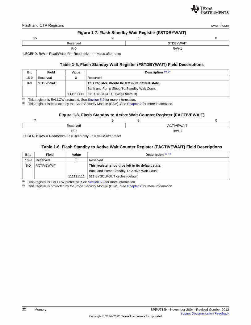
1-7. Flash Standby Wait Register (FSTDBYWAIT) ........................................................................ 22
1-8. Flash Standby to Active Wait Counter Register (FACTIVEWAIT) ................................................. 22
1-9. Flash Wait-State Register (FBANKWAIT) ............................................................................. 23
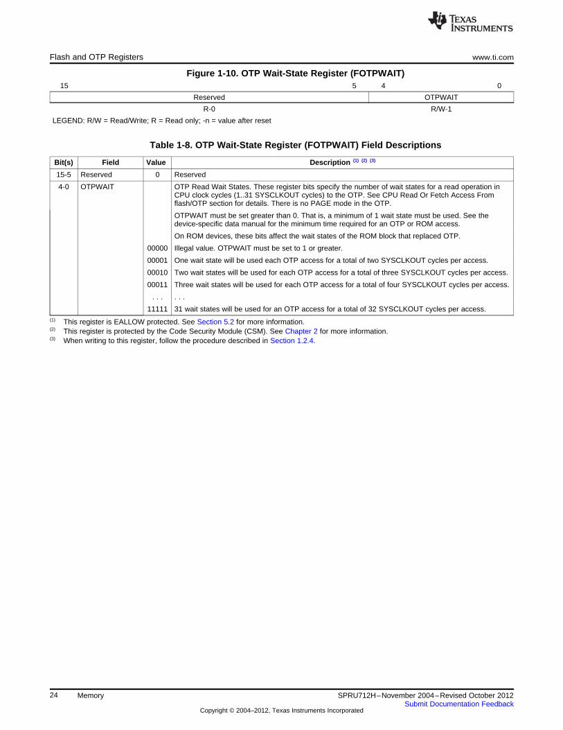
1-10. OTP Wait-State Register (FOTPWAIT) ................................................................................ 24
2-1. CSM Status and Control Register (CSMSCR)......................................................................... 29
2-2. Password Match Flow (PMF) ........................................................................................... 31
3-1. Clock and Reset Domains (280x/2801x) ............................................................................... 36
3-2. Clock and Reset Domains (28044) ..................................................................................... 37
3-3. Peripheral Clock Control 0 Register (PCLKCR0) ..................................................................... 38
3-4. Peripheral Clock Control 1 Register (PCLKCR1) ..................................................................... 40
3-5. Peripheral Clock Control 2 Register (PCLKCR2) (28044) ........................................................... 41
3-6. High-Speed Peripheral Clock Prescaler (HISPCP) Register ........................................................ 42
3-7. Low-Speed Peripheral Clock Prescaler Register (LOSPCP) ........................................................ 42
3-8. OSC and PLL Block....................................................................................................... 43
3-9. Oscillator Fail-Detection Logic Diagram ................................................................................ 44
3-10. XCLKOUT Generation .................................................................................................... 46
3-11. PLLCR Change Procedure Flow Chart ................................................................................. 47
3-12. PLLCR Register Layout .................................................................................................. 48
3-13. PLL Status Register (PLLSTS) .......................................................................................... 48
3-14. XCLKOUT Register (XCLK).............................................................................................. 50
3-15. Low Power Mode Control 0 Register (LPMCR0)...................................................................... 52
3-16. Watchdog Module ......................................................................................................... 53
3-17. System Control and Status Register (SCSR) ......................................................................... 56
3-18. Watchdog Counter Register (WDCNTR) ............................................................................... 57
3-19. Watchdog Reset Key Register (WDKEY) .............................................................................. 57
3-20. Watchdog Control Register (WDCR) ................................................................................... 57
3-21. CPU-Timers ................................................................................................................ 58
3-22. CPU-Timer Interrupt Signals and Output Signal ...................................................................... 59
3-23. TIMERxTIM Register (x = 0, 1, 2) ....................................................................................... 60
3-24. TIMERxTIMH Register (x = 0, 1, 2) ..................................................................................... 60
3-25. TIMERxPRD Register (x = 0, 1, 2) ...................................................................................... 60
3-26. TIMERxPRDH Register (x = 0, 1, 2) .................................................................................... 60
3-27. TIMERxTCR Register (x = 0, 1, 2) ...................................................................................... 61
3-28. TIMERxTPR Register (x = 0, 1, 2) ...................................................................................... 62
3-29. TIMERxTPRH Register (x = 0, 1, 2) ................................................................................... 62
4-1. Modes of Operation ....................................................................................................... 64
4-2. Input Qualification Using a Sampling Window ......................................................................... 68
4-3. Input Qualifier Clock Cycles.............................................................................................. 71
4-4. GPIO Port A MUX 1 (GPAMUX1) Register ............................................................................ 83
4-5. GPIO Port A MUX 2 (GPAMUX2) Register ............................................................................ 86
4-6. GPIO Port B MUX 1 (GPBMUX1) Register ............................................................................ 89
4 List of Figures SPRU712H–November 2004–Revised October 2012Submit Documentation Feedback
Copyright © 2004–2012, Texas Instruments Incorporated

www.ti.com
4-7. GPIO Port B MUX 2 (GPBMUX2) Register ............................................................................ 91
4-8. GPIO Port A Qualification Control (GPACTRL) Register ............................................................ 91
4-9. GPIO Port B Qualification Control (GPBCTRL) Register ............................................................ 92
4-10. GPIO Port A Qualification Select 1 (GPAQSEL1) Register.......................................................... 92
4-11. GPIO Port A Qualification Select 2 (GPAQSEL2) Register.......................................................... 93
4-12. GPIO Port B Qualification Select 1 (GPBQSEL1) Register.......................................................... 93
4-13. GPIO Port A Direction (GPADIR) Register ............................................................................ 94
4-14. GPIO Port B Direction (GPBDIR) Register ............................................................................ 94
4-15. GPIO Port A Pullup Disable (GPAPUD) Registers ................................................................... 95
4-16. GPIO Port B Pullup Disable (GPBPUD) Register .................................................................... 95
4-17. GPIO Port A Data (GPADAT) Register ................................................................................ 96
4-18. GPIO Port B Data (GPBDAT) Register ................................................................................ 97
4-19. GPIO Port A Set, Clear and Toggle (GPASET, GPACLEAR, GPATOGGLE) Registers ....................... 98
4-20. GPIO Port B Set, Clear and Toggle (GPBSET, GPBCLEAR, GPBTOGGLE) Register ......................... 99
4-21. GPIO XINT1, XINT2, XNMI Interrupt Select (GPIOXINT1SEL, GPIOXINT2SEL, GPIOXNMISEL)Registers ................................................................................................................. 100
4-22. GPIO Low Power Mode Wakeup Select (GPIOLPMSEL) Register ............................................... 101
4-23. GPIOA Miscellaneous Configuration Register (GPAMCFG) (28044 only) ....................................... 101
5-1. Device Configuration (DEVICECNF) Register ....................................................................... 109
5-2. Part ID Register .......................................................................................................... 110
5-3. REVID Register .......................................................................................................... 110
6-1. Overview: Multiplexing of Interrupts Using the PIE Block .......................................................... 113
6-2. Typical PIE/CPU Interrupt Response - INTx.y ....................................................................... 115
6-3. Reset Flow Diagram ..................................................................................................... 117
6-4. External and PIE Interrupt Sources.................................................................................... 118
6-5. Multiplexed Interrupt Request Flow Diagram......................................................................... 121
6-6. PIECTRL Register (Address CE0)..................................................................................... 135
6-7. PIE Interrupt Acknowledge Register (PIEACK) Register (Address CE1)......................................... 135
6-8. PIEIFRx Register (x = 1 to 12) ......................................................................................... 136
6-9. PIEIERx Register (x = 1 to 12) ......................................................................................... 136
6-10. Interrupt Flag Register (IFR) — CPU Register ...................................................................... 137
6-11. Interrupt Enable Register (IER) — CPU Register ................................................................... 139
6-12. Debug Interrupt Enable Register (DBGIER) — CPU Register .................................................... 141
6-13. External Interrupt 1 Control Register (XINT1CR) (Address 7070h) ............................................... 142
6-14. External Interrupt 2 Control Register (XINT2CR) (Address 7071h) ............................................... 142
6-15. External NMI Interrupt Control Register (XNMICR) — Address 7077h........................................... 143
6-16. External Interrupt 1 Counter (XINT1CTR) (Address 7078h) ....................................................... 144
6-17. External Interrupt 2 Counter (XINT2CTR) — Address 7079h...................................................... 144
6-18. External NMI Interrupt Counter (XNMICTR) (Address 707Fh)..................................................... 144
A-1. TMS320 ROM Code Prototype and Production Flowchart ......................................................... 147
5SPRU712H–November 2004–Revised October 2012 List of FiguresSubmit Documentation Feedback
Copyright © 2004–2012, Texas Instruments Incorporated

www.ti.com
List of Tables
1-1. Flash/OTP Configuration Registers ..................................................................................... 19
1-2. Flash Options Register (FOPT) Field Descriptions ................................................................... 20
1-3. Flash Power Register (FPWR) Field Descriptions .................................................................... 20
1-4. Flash Status Register (FSTATUS) Field Descriptions ................................................................ 21
1-5. Flash Standby Wait Register (FSTDBYWAIT) Field Descriptions .................................................. 22
1-6. Flash Standby to Active Wait Counter Register (FACTIVEWAIT) Field Descriptions ............................ 22
1-7. Flash Wait-State Register (FBANKWAIT) Field Descriptions ....................................................... 23
1-8. OTP Wait-State Register (FOTPWAIT) Field Descriptions .......................................................... 24
2-1. Security Levels............................................................................................................. 26
2-2. 280x Resources Affected by the CSM.................................................................................. 28
2-3. 280x Resources Not Affected by the CSM............................................................................. 28
2-4. Code Security Module (CSM) Registers ............................................................................... 29
2-5. CSM Status and Control Register (CSMSCR) Field Descriptions .................................................. 29
3-1. PLL, Clocking, Watchdog, and Low-Power Mode Registers ........................................................ 38
3-2. Peripheral Clock Control 0 Register (PCLKCR0) Field Descriptions ............................................... 39
3-3. Peripheral Clock Control 1 Register (PCLKCR1) Field Descriptions .............................................. 40
3-4. Peripheral Clock Control 2 Register (PCLKCR2) Field Descriptions (28044 only) ............................... 41
3-5. High-Speed Peripheral Clock Prescaler (HISPCP) Field Descriptions ............................................. 42
3-6. Low-Speed Peripheral Clock Prescaler Register (LOSPCP) Field Descriptions.................................. 42
3-7. Possible PLL Configuration Modes ..................................................................................... 43
3-8. PLLCR Bit Descriptions................................................................................................... 48
3-9. PLL Status Register (PLLSTS) Field Descriptions .................................................................... 49
3-10. XCLKOUT Register (XCLK) Field Descriptions ....................................................................... 50
3-11. 280x Low-Power Modes .................................................................................................. 50
3-12. Low Power Modes......................................................................................................... 51
3-13. Low Power Mode Control 0 Register (LPMCR0) Field Descriptions ............................................... 52
3-14. Example Watchdog Key Sequences.................................................................................... 54
3-15. System Control and Status Register (SCSR) Field Descriptions ................................................... 56
3-16. Watchdog Counter Register (WDCNTR) Field Descriptions......................................................... 57
3-17. Watchdog Reset Key Register (WDKEY) Field Descriptions ........................................................ 57
3-18. Watchdog Control Register (WDCR) Field Descriptions ............................................................. 57
3-19. CPU-Timers 0, 1, 2 Configuration and Control Registers ............................................................ 59
3-20. TIMERxTIM Register Field Descriptions ............................................................................... 60
3-21. TIMERxTIMH Register Field Descriptions ............................................................................. 60
3-22. TIMERxPRD Register Field Descriptions .............................................................................. 60
3-23. TIMERxPRDH Register Field Descriptions ............................................................................ 60
3-24. TIMERxTCR Register Field Descriptions............................................................................... 61
3-25. TIMERxTPR Register Field Descriptions............................................................................... 62
3-26. TIMERxTPRH Register Field Descriptions............................................................................. 62
4-1. GPIO Control Registers................................................................................................... 65
4-2. GPIO Interrupt and Low Power Mode Select Registers.............................................................. 65
4-3. GPIO Data Registers ..................................................................................................... 66
4-4. Sampling Period ........................................................................................................... 69
4-5. Sampling Frequency ...................................................................................................... 69
4-6. Case 1: Three-Sample Sampling Window Width...................................................................... 70
4-7. Case 2: Six-Sample Sampling Window Width ......................................................................... 70
4-8. Default State of Peripheral Input ........................................................................................ 73
6 List of Tables SPRU712H–November 2004–Revised October 2012Submit Documentation Feedback
Copyright © 2004–2012, Texas Instruments Incorporated
www.ti.com
4-9. 2809 and 2808 GPIO MUX .............................................................................................. 74
4-10. 2806 GPIO MUX........................................................................................................... 75
4-11. 2801 and 2802 GPIO MUX .............................................................................................. 76
4-12. TMS320F28016/TMS320F28015 GPIO MUX ........................................................................ 77
4-13. F28044 GPIO MUX ....................................................................................................... 78
4-14. Peripheral to GPIO Cross Reference ................................................................................... 80
4-15. GPIO Port A MUX 1 (GPAMUX1) Register Field Descriptions...................................................... 83
4-16. GPIO Port A MUX 2 (GPAMUX2) Register Field Descriptions...................................................... 87
4-17. GPIO Port B MUX 1 (GPBMUX1) Register Field Descriptions...................................................... 89
4-18. GPIO Port B MUX 2 (GPBMUX2) Register Field Descriptions...................................................... 91
4-19. GPIO Port A Qualification Control (GPACTRL) Register Field Descriptions ...................................... 91
4-20. GPIO Port B Input Qualification Control (GPBCTRL) Register Field Descriptions ............................... 92
4-21. GPIO Port A Qualification Select 1 (GPAQSEL1) Register Field Descriptions ................................... 92
4-22. GPIO Port A Qualification Select 2 (GPAQSEL2) Register Field Descriptions ................................... 93
4-23. GPIO Port B Qualification Select 1 (GPBQSEL1) Register Field Descriptions ................................... 93
4-24. GPIO Port B Qualification Select 2 (GPBQSEL2) Register Field Descriptions ................................... 93
4-25. GPIO Port A Direction (GPADIR) Register Field Descriptions ...................................................... 94
4-26. GPIO Port B Direction (GPBDIR) Register Field Descriptions ...................................................... 94
4-27. GPIO Port A Internal Pullup Disable (GPAPUD) Register Field Descriptions..................................... 95
4-28. GPIO Port B Internal Pullup Disable (GPBPUD) Register Field Descriptions..................................... 95
4-29. GPIO Port A Data (GPADAT) Register Field Descriptions .......................................................... 96
4-30. GPIO Port B Data (GPBDAT) Register Field Descriptions .......................................................... 97
4-31. GPIO Port A Set (GPASET) Register Field Descriptions ............................................................ 98
4-32. GPIO Port A Clear (GPACLEAR) Register Field Descriptions ...................................................... 98
4-33. GPIO Port A Toggle (GPATOGGLE) Register Field Descriptions .................................................. 98
4-34. GPIO Port B Set (GPBSET) Register Field Descriptions ............................................................ 99
4-35. GPIO Port B Clear (GPBCLEAR) Register Field Descriptions ...................................................... 99
4-36. GPIO Port B Toggle (GPBTOGGLE) Register Field Descriptions .................................................. 99
4-37. GPIO XINT1 Interrupt Select (GPIOXINT1SEL) Register Field Descriptions .................................... 100
4-38. GPIO XINT2 Interrupt Select (GPIOXINT2SEL) Register Field Descriptions .................................... 100
4-39. GPIO XNMI Interrupt Select (GPIOXNMISEL) Register Field Descriptions...................................... 100
4-40. GPIO Low Power Mode Wakeup Select (GPIOLPMSEL) Register Field Descriptions......................... 101
4-41. GPIOA Miscellaneous Configuration Register (GPAMCFG) Field Descriptions (28044 only) ................. 101
5-1. Peripheral Frame 0 Registers .......................................................................................... 103
5-2. Peripheral Frame 1 Registers .......................................................................................... 103
5-3. Peripheral Frame 2 Registers .......................................................................................... 104
5-4. Access to EALLOW-Protected Registers ............................................................................. 104
5-5. EALLOW-Protected Device Emulation Registers.................................................................... 105
5-6. EALLOW-Protected Flash/OTP Configuration Registers ........................................................... 105
5-7. EALLOW-Protected Code Security Module (CSM) Registers ..................................................... 105
5-8. EALLOW-Protected PIE Vector Table ................................................................................ 105
5-9. EALLOW-Protected PLL, Clocking, Watchdog, and Low-Power Mode Registers .............................. 106
5-10. EALLOW-Protected GPIO MUX Registers .......................................................................... 106
5-11. EALLOW-Protected eCAN-A Registers ............................................................................... 107
5-12. EALLOW-Protected ePWM1 - ePWM16 Registers.................................................................. 107
5-13. Device Emulation Registers ............................................................................................ 109
5-14. DEVICECNF Register Field Descriptions............................................................................. 109
5-15. PARTID Register Field Descriptions .................................................................................. 110
5-16. REVID Register Field Descriptions .................................................................................... 110
7SPRU712H–November 2004–Revised October 2012 List of TablesSubmit Documentation Feedback
Copyright © 2004–2012, Texas Instruments Incorporated

www.ti.com
5-17. PROTSTART and PROTRANGE Registers.......................................................................... 111
5-18. PROTSTART Valid Values ............................................................................................ 111
5-19. PROTRANGE Valid Values ............................................................................................ 111
6-1. Enabling Interrupt ........................................................................................................ 115
6-2. Interrupt Vector Table Mapping ....................................................................................... 116
6-3. Vector Table Mapping After Reset Operation ....................................................................... 116
6-4. 280x, 2801x PIE MUXed Peripheral Interrupt Vector Table........................................................ 123
6-5. 28044 PIE MUXed Peripheral Interrupt Vector Table ............................................................... 124
6-6. 280x/2801x PIE Vector Table .......................................................................................... 125
6-7. 28044 PIE Vector Table................................................................................................. 129
6-8. PIE Configuration and Control Registers ............................................................................. 134
6-9. PIECTRL Register Address Field Descriptions ...................................................................... 135
6-10. PIE Interrupt Acknowledge Register (PIEACK) Field Descriptions................................................ 135
6-11. PIEIFRx Register Field Descriptions .................................................................................. 136
6-12. PIEIERx Register (x = 1 to 12) Field Descriptions................................................................... 136
6-13. Interrupt Flag Register (IFR) — CPU Register Field Descriptions ................................................ 137
6-14. Interrupt Enable Register (IER) — CPU Register Field Descriptions ............................................. 139
6-15. Debug Interrupt Enable Register (DBGIER) — CPU Register Field Descriptions .............................. 141
6-16. External Interrupt 1 Control Register (XINT1CR) Field Descriptions.............................................. 142
6-17. External Interrupt 2 Control Register (XINT2CR) Field Descriptions.............................................. 143
6-18. External NMI Interrupt Control Register (XNMICR) Field Descriptions ........................................... 143
6-19. XNMICR Register Settings and Interrupt Sources................................................................... 143
6-20. External Interrupt 1 Counter (XINT1CTR) Field Descriptions ...................................................... 144
6-21. External Interrupt 2 Counter (XINT2CTR) Field Descriptions ...................................................... 144
6-22. External NMI Interrupt Counter (XNMICTR) Field Descriptions ................................................... 144
B-1. Technical Changes ...................................................................................................... 150
8 List of Tables SPRU712H–November 2004–Revised October 2012Submit Documentation Feedback
Copyright © 2004–2012, Texas Instruments Incorporated

PrefaceSPRU712H–November 2004–Revised October 2012
Read This First
About This Manual
This reference guide is applicable for the systems control and interrupts found on theTMS320x280x/TMS320x2801x/TMS320x2804x digital signal processors. This includes all Flash-based,ROM-based, and RAM-based devices within the 280x family.
This guide describes how various 280x digital signal processor (DSP) system controls and interrupts workwith peripherals. It includes information on the:
• Flash and one-time programmable (OTP) memories
• Code security module (CSM), which is a security feature incorporated in TMS320C28x™ devices.
• Clocking mechanisms including the oscillator, PLL, XCLKOUT, watchdog module, and the low-powermodes. In addition, the 32-bit CPU-Timers are also described.
• GPIO MUX registers used to select the operation of shared pins on the 280x devices.
• Accessing the peripheral frames to write to and read from various peripheral registers on the device.
• Interrupt sources both external and the peripheral interrupt expansion (PIE) block that multiplexesnumerous interrupt sources into a smaller set of interrupt inputs.
Notational Conventions
This document uses the following conventions.
• Hexadecimal numbers are shown with the suffix h or with a leading 0x. For example, the followingnumber is 40 hexadecimal (decimal 64): 40h or 0x40.
• Registers in this document are shown in figures and described in tables.
– Each register figure shows a rectangle divided into fields that represent the fields of the register.Each field is labeled with its bit name, its beginning and ending bit numbers above, and itsread/write properties below. A legend explains the notation used for the properties.
– Reserved bits in a register figure designate a bit that is used for future device expansion.
Related Documentation From Texas Instruments
The following books describe the TMS320x280x and related support tools that are available on the TIwebsite:
Data Manuals—SPRS230 — TMS320F2809, F2808, F2806, F2802, F2801, C2802, C2801, and F2801x DSPs Data
Manual contains the pinout, signal descriptions, as well as electrical and timing specifications forthe F280x devices.
SPRZ171 — TMS320F280x, TMS320C280x, and TMS320F2801x DSP Silicon Erratadescribes the advisories and usage notes for different versions of silicon.
SPRS357 — TMS320F28044 Digital Signal Processor Data Manual contains the pinout, signaldescriptions, as well as electrical and timing specifications for the F28044 device.
SPRZ255 — TMS320F28044 DSP Silicon Erratadescribes the advisories and usage notes for different versions of silicon.
CPU User's Guides—
9SPRU712H–November 2004–Revised October 2012 Read This FirstSubmit Documentation Feedback
Copyright © 2004–2012, Texas Instruments Incorporated

Related Documentation From Texas Instruments www.ti.com
SPRU430 — TMS320C28x CPU and Instruction Set Reference Guide describes the central processingunit (CPU) and the assembly language instructions of the TMS320C28x fixed-point digital signalprocessors (DSPs). It also describes emulation features available on these DSPs.
SPRU712 — TMS320x280x, 2801x, 2804x System Control and Interrupts Reference Guide describesthe various interrupts and system control features of the 280x digital signal processors (DSPs).
Peripheral Guides —SPRU566 — TMS320x28xx, 28xxx DSP Peripheral Reference Guide describes the peripheral
reference guides of the 28x digital signal processors (DSPs).
SPRU716 — TMS320x280x, 2801x, 2804x Analog-to-Digital Converter (ADC) Reference Guidedescribes how to configure and use the on-chip ADC module, which is a 12-bit pipelined ADC.
SPRU791 — TMS320x280x, 2801x, 2804x Enhanced Pulse Width Modulator (ePWM) ModuleReference Guide describes the main areas of the enhanced pulse width modulator that includedigital motor control, switch mode power supply control, UPS (uninterruptible power supplies), andother forms of power conversion
SPRU790 — TMS320x280x, 2801x, 2804x Enhanced Quadrature Encoder Pulse (eQEP) ReferenceGuide describes the eQEP module, which is used for interfacing with a linear or rotary incrementalencoder to get position, direction, and speed information from a rotating machine in highperformance motion and position control systems. It includes the module description and registers
SPRU807 — TMS320x280x, 2801x, 2804x Enhanced Capture (eCAP) Module Reference Guidedescribes the enhanced capture module. It includes the module description and registers.
SPRU924 — TMS320x280x, 2801x, 2804x High-Resolution Pulse Width Modulator (HRPWM)describes the operation of the high-resolution extension to the pulse width modulator (HRPWM)
SPRU074 — TMS320x280x, 2801x, 2804x Enhanced Controller Area Network (eCAN) ReferenceGuide describes the eCAN that uses established protocol to communicate serially with othercontrollers in electrically noisy environments.
SPRU051 — TMS320x280x, 2801x, 2804x Serial Communication Interface (SCI) Reference Guidedescribes the SCI, which is a two-wire asynchronous serial port, commonly known as a UART. TheSCI modules support digital communications between the CPU and other asynchronous peripheralsthat use the standard non-return-to-zero (NRZ) format.
SPRU059 — TMS320x280x, 2801x, 2804x Serial Peripheral Interface (SPI) Reference Guidedescribes the SPI - a high-speed synchronous serial input/output (I/O) port - that allows a serial bitstream of programmed length (one to sixteen bits) to be shifted into and out of the device at aprogrammed bit-transfer rate.
SPRU721 — TMS320x280x, 2801x, 2804x Inter-Integrated Circuit (I2C) Reference Guide describesthe features and operation of the inter-integrated circuit (I2C) module.
SPRU722 — TMS320x280x, 2801x, 2804x Boot ROM Reference Guide describes the purpose andfeatures of the bootloader (factory-programmed boot-loading software). It also describes othercontents of the device on-chip boot ROM and identifies where all of the information is located withinthat memory.
Tools Guides—SPRU513 — TMS320C28x Assembly Language Tools v5.0.0 User's Guide describes the assembly
language tools (assembler and other tools used to develop assembly language code), assemblerdirectives, macros, common object file format, and symbolic debugging directives for theTMS320C28x device.
SPRU514 — TMS320C28x Optimizing C/C++ Compiler v5.0.0 User's Guide describes theTMS320C28x™ C/C++ compiler. This compiler accepts ANSI standard C/C++ source code andproduces TMS320 DSP assembly language source code for the TMS320C28x device.
10 Read This First SPRU712H–November 2004–Revised October 2012Submit Documentation Feedback
Copyright © 2004–2012, Texas Instruments Incorporated

www.ti.com Related Documentation From Texas Instruments
SPRU608 — TMS320C28x Instruction Set Simulator Technical Overview describes the simulator,available within the Code Composer Studio for TMS320C2000 IDE, that simulates the instructionset of the C28x™ core.
SPRU625 — TMS320C28x DSP/BIOS 5.32 Application Programming Interface (API) ReferenceGuide describes development using DSP/BIOS.
Application Reports—
SPRAAM0 — Getting Started With TMS320C28x Digital Signal Controllers is organized bydevelopment flow and functional areas to make your design effort as seamless as possible. Tips ongetting started with C28x™ DSP software and hardware development are provided to aid in yourinitial design and debug efforts. Each section includes pointers to valuable information includingtechnical documentation, software, and tools for use in each phase of design.
SPRAAD5 — Power Line Communication for Lighting Applications Using Binary Phase ShiftKeying (BPSK) with a Single DSP Controller presents a complete implementation of a power linemodem following CEA-709 protocol using a single DSP.
SPRAA85 — Programming TMS320x28xx and 28xxx Peripherals in C/C++ explores a hardwareabstraction layer implementation to make C/C++ coding easier on 28x DSPs. This method iscompared to traditional #define macros and topics of code efficiency and special case registers arealso addressed.
SPRA958 — Running an Application from Internal Flash Memory on the TMS320F28xxx DSP coversthe requirements needed to properly configure application software for execution from on-chip flashmemory. Requirements for both DSP/BIOS™ and non-DSP/BIOS projects are presented. Examplecode projects are included.
SPRAA91 — TMS320F280x Digital Signal Controller USB Connectivity Using TUSB3410 USB-to-UART Bridge Chip presents hardware connections as well as software preparation and operationof the development system using a simple communication echo program.
SPRAAD8 — TMS320x280x and TMS320F2801x ADC Calibration describes a method for improvingthe absolute accuracy of the 12-bit ADC found on the TMS320x280x and TMS320F2801x devices.Inherent gain and offset errors affect the absolute accuracy of the ADC. The methods described inthis report can improve the absolute accuracy of the ADC to levels better than 0.5%. Thisapplication report has an option to download an example program that executes from RAM on theF2808 EzDSP.
SPRAAI1 — Using the ePWM Module for 0% – 100% Duty Cycle Control provides a guide for the useof the ePWM module to provide 0% to 100% duty cycle control and is applicable to theTMS320x280x family of processors.
SPRAA88 — Using PWM Output as a Digital-to-Analog Converter on a TMS320F280x Digital SignalController presents a method for utilizing the on-chip pulse width modulated (PWM) signalgenerators on the TMS320F280x family of digital signal controllers as a digital-to-analog converter(DAC).
SPRAAH1 — Using the Enhanced Quadrature Encoder Pulse (eQEP) Module in TMS320x280x,28xxx as a Dedicated Capture provides a guide for the use of the eQEP module as a dedicatedcapture unit and is applicable to the TMS320x280x, 28xxx family of processors.
SPRA820 — Online Stack Overflow Detection on the TMS320C28x DSP presents the methodology foronline stack overflow detection on the TMS320C28x™ DSP. C-source code is provided thatcontains functions for implementing the overflow detection on both DSP/BIOS™ and non-DSP/BIOS applications.
SPRA806 — An Easy Way of Creating a C-callable Assembly Function for the TMS320C28x DSPprovides instructions and suggestions to configure the C compiler to assist with understanding ofparameter-passing conventions and environments expected by the C compiler.
TMS320C28x, C28x, Code Composer Studio are trademarks of Texas Instruments.All other trademarks are the property of their respective owners.
11SPRU712H–November 2004–Revised October 2012 Read This FirstSubmit Documentation Feedback
Copyright © 2004–2012, Texas Instruments Incorporated

Chapter 1SPRU712H–November 2004–Revised October 2012
Memory
This chapter describes the proper sequence to configure the wait states and operating mode of flash andone-time programmable (OTP) memories on a 28x digital signal processor (DSP) device. It also includesinformation on flash and OTP power modes and how to improve flash performance by enabling the flashpipeline mode.
On ROM-only devices, this information applies to the ROM that replaces the flash and the OTP.
Topic ........................................................................................................................... Page
1.1 Flash and OTP Memory ...................................................................................... 131.2 Flash and OTP Power Modes .............................................................................. 131.3 Flash and OTP Registers .................................................................................... 19
12 Memory SPRU712H–November 2004–Revised October 2012Submit Documentation Feedback
Copyright © 2004–2012, Texas Instruments Incorporated

www.ti.com Flash and OTP Memory
1.1 Flash and OTP Memory
This section describes how to configure two kinds of memory - flash and one-time programmable (OTP).On ROM only devices, this information applies to the ROM that replaces the flash and the OTP.
1.1.1 Flash Memory
The on-chip flash is uniformly mapped in both program and data memory space. This flash memory isalways enabled on 28x devices and features:
• Multiple sectorsThe minimum amount of flash memory that can be erased is a sector. Having multiple sectors providesthe option of leaving some sectors programmed and only erasing specific sectors.
• Code securityThe flash is protected by the Code Security Module (CSM). By programming a password into the flash,the user can prevent access to the flash by unauthorized persons. See Chapter 2 for information inusing the Code Security Module.
• Low power modesTo save power when the flash is not in use, two levels of low power modes are available. SeeSection 1.2 for more information on the available flash power modes.
• Configurable wait statesConfigurable wait states can be adjusted based on CPU frequency to give the best performance for agiven execution speed.
• Enhanced performanceA flash pipeline mode is provided to improve performance of linear code execution.
1.1.2 OTP Memory
The 1K x 16 block of one-time programmable (OTP) memory is uniformly mapped in both program anddata memory space. Thus, the OTP can be used to program data or code. This block, unlike flash, can beprogrammed only one time and cannot be erased.
1.2 Flash and OTP Power Modes
The following operating states apply to the flash and OTP memory:
• Reset or Sleep StateThis is the state after a device reset. In this state, the bank and pump are in a sleep state (lowestpower). When the flash is in the sleep state, a CPU data read or opcode fetch to the flash or OTPmemory map area will automatically initiate a change in power modes to the standby state and then tothe active state. During this transition time to the active state, the CPU will automatically be stalled.Once the transition to the active state is completed, the CPU access will complete as normal.
• Standby StateIn this state, the bank and pump are in standby power mode state. This state uses more power thenthe sleep state, but takes a shorter time to transition to the active or read state. When the flash is inthe standby state, a CPU data read or opcode fetch to the flash or OTP memory map area willautomatically initiate a change in power modes to the active state. During this transition time to theactive state, the CPU will automatically be stalled. Once the flash/OTP has reached the active state,the CPU access will complete as normal.
• Active or Read StateIn this state, the bank and pump are in active power mode state (highest power). The CPU read orfetch access wait states to the flash/OTP memory map area is controlled by the FBANKWAIT andFOTPWAIT registers. A prefetch mechanism called flash pipeline can also be enabled to improve fetchperformance for linear code execution.
13SPRU712H–November 2004–Revised October 2012 MemorySubmit Documentation Feedback
Copyright © 2004–2012, Texas Instruments Incorporated
Activestate
stateStandby
stateSleep
DelayFACTIVEWAIT
cycles
DelayFSTDBYWAIT
cyclesFSTDBYWAIT
cycles
FACTIVEWAIT
Delay
cycles
Delay
Highestpower
Lowest powerLongest
Wake up time
PWR=0,1
PWR=0,0
PWR=0,0
PWR=1,1or access tothe Flash/OTP
PWR=0,1
PWR=1,1or access to
the Flash/OTP
Reset
Flash and OTP Power Modes www.ti.com
NOTE: During the boot process, the 280x Boot ROM performs a dummy read of the Code SecurityModule (CSM) password locations located in the flash. This read is performed to unlock anew or erased device that has no password stored in it so that flash programming or loadingof code into CSM protected SARAM can be performed. On devices with a password stored,this read has no affect and the CSM remains locked (see Chapter 2 for information on theCSM). One effect of this read is that the flash will transition from the sleep (reset) state to theactive state.
The flash/OTP bank and pump are always in the same power mode. See Figure 1-1 for a graphicdepiction of the available power states. You can change the current flash/OTP memory power state asfollows:
• To move to a lower power stateChange the PWR mode bits from a higher power mode to a lower power mode. This changeinstantaneously moves the flash/OTP bank to the lower power state. This register should be accessedonly by code running outside the flash/OTP memory.
• To move to a higher power stateTo move from a lower power state to a higher power state, there are two options.
1. Change the FPWR register from a lower state to a higher state. This access brings the flash/OTPmemory to the higher state.
2. Access the flash or OTP memory by a read access or program opcode fetch access. This accessautomatically brings the flash/OTP memory to the active state.
There is a delay when moving from a lower power state to a higher one. See Figure 1-1. This delay isrequired to allow the flash to stabilize at the higher power mode. If any access to the flash/OTP memoryoccurs during this delay the CPU automatically stalls until the delay is complete.
Figure 1-1. Flash Power Mode State Diagram
14 Memory SPRU712H–November 2004–Revised October 2012Submit Documentation Feedback
Copyright © 2004–2012, Texas Instruments Incorporated
www.ti.com Flash and OTP Power Modes
The duration of the delay is determined by the FSTDBYWAIT and FACTIVEWAIT registers. Moving fromthe sleep state to a standby state is delayed by a count determined by the FSTDBYWAIT register. Movingfrom the standby state to the active state is delayed by a count determined by the FACTIVEWAIT register.Moving from the sleep mode (lowest power) to the active mode (highest power) is delayed byFSTDBYWAIT + FACTIVEWAIT. These registers should be left in their default state.
1.2.1 Flash and OTP Performance
CPU read or data fetch operations to the flash/OTP can take one of the following forms:
• 32-bit instruction fetch
• 16-bit or 32-bit data space read
• 16-bit program space read
Once flash is in the active power state, then a read or fetch access to the bank memory map area can beclassified as a flash access or an OTP access.
The main flash array is organized into rows and columns. The rows contain 2048 bits of information.Accesses to flash and OTP are one of three types:
1. Flash Memory Random AccessThe first access to a 2048 bit row is considered a random access.
2. Flash Memory Paged AccessWhile the first access to a row is considered a random access, subsequent accesses within the samerow are termed paged accesses.
The number of wait states for both a random and a paged access can be configured by programmingthe FBANKWAIT register. The number of wait states used by a random access is controlled by theRANDWAIT bits and the number of wait states used by a paged access is controlled by thePAGEWAIT bits. The FBANKWAIT register defaults to a worst-case wait state count and, thus, needsto be initialized for the appropriate number of wait states to improve performance based on the CPUclock rate and the access time of the flash. The flash supports 0-wait accesses when the PAGEWAITbits are set to zero. This assumes that the CPU speed is low enough to accommodate the accesstime. To determine the random and paged access time requirements, refer to the Data Manual for yourparticular device.
On ROM devices, the same wait-state configuration is preserved to allow timing compatibility with theflash devices.
3. OTP AccessRead or fetch accesses to the OTP are controlled by the OTPWAIT bits in the FOTPWAIT register.Accesses to the OTP take longer than the flash and there is no paged mode. As with flash, the OTPreplaced with ROM on ROM only devices allow the same wait-state configuration for OTP. Todetermine OTP access time requirements, see the data manual for your particular device.
Some other points to keep in mind when working with flash:
• CPU writes to the flash or OTP memory map area are ignored. They complete in a single cycle.
• When the Code Security Module (CSM) is secured, reads to the flash/OTP memory map area fromoutside the secure zone take the same number of cycles as a normal access. However, the readoperation returns a zero.
• Reads of the CSM password locations are hardwired for 16 wait-states. The PAGEWAIT andRANDOMWAIT bits have no effect on these locations. See Chapter 2 for more information on theCSM.
15SPRU712H–November 2004–Revised October 2012 MemorySubmit Documentation Feedback
Copyright © 2004–2012, Texas Instruments Incorporated

Flash Pipeline
CPU 32 bitsMUX
Data read from either program or data memory
Instruction Fetch (64 bits)
Flash or OTPRead
16 bits
Flash and OTP
Instruction buffer
64-bitBuffer
64-bitBuffer
Flash and OTP Power Modes www.ti.com
1.2.2 28x Flash Pipeline Mode
Flash memory is typically used to store application code. During code execution, instructions are fetchedfrom sequential memory addresses, except when a discontinuity occurs. Usually the portion of the codethat resides in sequential addresses makes up the majority of the application code and is referred to aslinear code. To improve the performance of linear code execution, a flash pipeline mode has beenimplemented. The flash pipeline feature is disabled by default. Setting the ENPIPE bit in the FOPT registerenables this mode. The flash pipeline mode is independent of the CPU pipeline. To allow you to maintaincode timing compatibility between flash and ROM devices, the flash pipeline mode has also beenimplemented on ROM devices.
An instruction fetch from the flash or OTP reads out 64 bits per access. The starting address of the accessfrom flash is automatically aligned to a 64-bit boundary such that the instruction location is within the 64bits to be fetched. With flash pipeline mode enabled (see Figure 1-2), the 64 bits read from the instructionfetch are stored in a 64-bit wide by 2-level deep instruction pre-fetch buffer. The contents of this pre-fetchbuffer are then sent to the CPU for processing as required.
Up to two 32-bit instructions or up to four 16-bit instructions can reside within a single 64-bit access. Themajority of C28x instructions are 16 bits, so for every 64-bit instruction fetch from the flash bank it is likelythat there are up to four instructions in the pre-fetch buffer ready to process through the CPU. During thetime it takes to process these instructions, the flash pipeline automatically initiates another access to theflash bank to pre-fetch the next 64 bits. In this manner, the flash pipeline mode works in the background tokeep the instruction pre-fetch buffers as full as possible. Using this technique, the overall efficiency ofsequential code execution from flash or OTP is improved significantly.
Figure 1-2. Flash Pipeline
The flash pipeline pre-fetch is aborted only on a PC discontinuity caused by executing an instruction suchas a branch, BANZ, call, or loop. When this occurs, the pre-fetch is aborted and the contents of the pre-fetch buffer are flushed. There are two possible scenarios when this occurs:
1. If the destination address is within the flash or OTP, the pre-fetch aborts and then resumes at thedestination address.
2. If the destination address is outside of the flash and OTP, the pre-fetch is aborted and begins againonly when a branch is made back into the flash or OTP. The flash pipeline pre-fetch mechanism onlyapplies to instruction fetches from program space. Data reads from data memory and from programmemory do not utilize the pre-fetch buffer capability and thus bypass the pre-fetch buffer. For example,instructions such as MAC, DMAC, and PREAD read a data value from program memory. When thisread happens, the pre-fetch buffer is bypassed but the buffer is not flushed. If an instruction pre-fetchis already in progress when a data read operation is initiated, then the data read will be stalled until thepre-fetch completes.
16 Memory SPRU712H–November 2004–Revised October 2012Submit Documentation Feedback
Copyright © 2004–2012, Texas Instruments Incorporated

www.ti.com Flash and OTP Power Modes
1.2.3 Reserved Locations Within Flash and OTP
When allocating code and data to flash and OTP memory, keep the following in mind:
1. Address locations 0x3F7FF6 and 0x3F7FF7 are reserved for an "entry into flash" branch instruction.When the "boot to flash" boot option is used, the boot ROM will jump to address 0x3F7FF6. A branchinstruction programmed here by the user will then re-direct code execution to the entry point of theapplication.
2. For code security operation, all addresses between 0x3F7F80 and 0x3F7FF5 cannot be used asprogram code or data, but must be programmed to 0x0000 when the Code Security Password isprogrammed. If security is not a concern, addresses 0x3F7F80 through 0x3F7FEF may be used forcode or data. See Chapter 2 for information in using the Code Security Module.
3. Addresses from 0x3F7FF0 to 0x3F7FF5 are reserved for data variables and should not containprogram code.
4. If the application will be migrated to ROM at a later time, certain locations in the flash and OTP will beused by TI to store a checksum and device number identifier. These locations are documented in thechapter on submitting ROM codes to TI in the TMS320C28x DSP CPU and Instruction Set ReferenceGuide (SPRU430).
1.2.4 Procedure to Change the Flash Configuration Registers
During flash configuration, no accesses to the flash or OTP can be in progress. This includes instructionsstill in the CPU pipeline, data reads, and instruction pre-fetch operations. To be sure that no access takesplace during the configuration change, you should follow the procedure shown in Figure 1-3 for any codethat modifies the FOPT, FPWR, FBANKWAIT, or FOTPWAIT registers.
This procedure also applies to the ROM on devices where the flash and OTP have been replaced withROM.
17SPRU712H–November 2004–Revised October 2012 MemorySubmit Documentation Feedback
Copyright © 2004–2012, Texas Instruments Incorporated

Wait eight cycles to let the write instructionspropagate through the CPU pipeline. Thismust be done before the return-from-functioncall is made.
Write instructions to FOPT, FBANKWAIT,etc.
The function that changes the configurationcannot execute from the Flash or OTP.
Branch or call is required to properly flush theCPU pipeline before the configurationchange.
Wait 8 cycles (8 NOPs)
Return to calling function
Continue executionSARAM, Flash,OTP, or ROM
Flash configurationchange
Do not execute fromFlash/OTP
SARAM
Begin Flash configurationchange
SARAM, Flash,OTP, ROM
Branch or call toconfiguration code
Flash and OTP Power Modes www.ti.com
Figure 1-3. Flash Configuration Access Flow Diagram
18 Memory SPRU712H–November 2004–Revised October 2012Submit Documentation Feedback
Copyright © 2004–2012, Texas Instruments Incorporated

www.ti.com Flash and OTP Registers
1.3 Flash and OTP Registers
The flash and OTP memory can be configured by the registers shown in Table 1-1. The configurationregisters are all EALLOW protected. The bit descriptions are in Figure 1-4 through Figure 1-10.
Table 1-1. Flash/OTP Configuration Registers
Name (1) (2) Address Size (x16) Description Bit Description
FOPT 0x0A80 1 Flash Option Register Figure 1-4
Reserved 0x0A81 1 Reserved
FPWR 0x0A82 1 Flash Power Modes Register Figure 1-5
FSTATUS 0x0A83 1 Status Register Figure 1-6
FSTDBYWAIT (3) 0x0A84 1 Flash Sleep To Standby Wait Register Figure 1-7
FACTIVEWAIT (3) 0x0A85 1 Flash Standby To Active Wait Register Figure 1-8
FBANKWAIT 0x0A86 1 Flash Read Access Wait State Register Figure 1-9
FOTPWAIT 0x0A87 1 OTP Read Access Wait State Register Figure 1-10(1) These registers are EALLOW protected. See Section 5.2 for information.(2) These registers are protected by the Code Security Module (CSM). See Chapter 2 for more information.(3) These registers should be left in their default state.
NOTE: The flash configuration registers should not be written to by code that is running from OTP orflash memory or while an access to flash or OTP may be in progress. All register accessesto the flash registers should be made from code executing outside of flash/OTP memory andan access should not be attempted until all activity on the flash/OTP has completed. Nohardware is included to protect against this.
To summarize, you can read the flash registers from code executing in flash/OTP; however,do not write to the registers.
CPU write access to the flash configuration registers can be enabled only by executing the EALLOWinstruction. Write access is disabled when the EDIS instruction is executed. This protects the registersfrom spurious accesses. Read access is always available. The registers can be accessed through theJTAG port without the need to execute EALLOW. See Section 5.2 for information on EALLOW protection.These registers support both 16-bit and 32-bit accesses.
19SPRU712H–November 2004–Revised October 2012 MemorySubmit Documentation Feedback
Copyright © 2004–2012, Texas Instruments Incorporated

Flash and OTP Registers www.ti.com
Figure 1-4. Flash Options Register (FOPT)15 1 0
Reserved ENPIPE
R-0 R/W-0
LEGEND: R/W = Read/Write; R = Read only; -n = value after reset
Table 1-2. Flash Options Register (FOPT) Field Descriptions
Bit Field Value Description (1) (2) (3)
15-1 Reserved
0 ENPIPE Enable Flash Pipeline Mode Bit. Flash pipeline mode is active when this bit is set. The pipelinemode improves performance of instruction fetches by pre-fetching instructions. See Section 1.2.2for more information.
When pipeline mode is enabled, the flash wait states (paged and random) must be greater thanzero.
On flash devices, ENPIPE affects fetches from flash and OTP. On ROM devices, ENPIPE affectsfetches from the ROM blocks that replaced the flash and OTP.
0 Flash Pipeline mode is not active. (default)
1 Flash Pipeline mode is active.(1) This register is EALLOW protected. See Section 5.2 for more information.(2) This register is protected by the Code Security Module (CSM). See Chapter 2 for more information.(3) When writing to this register, follow the procedure described in Section 1.2.4.
Figure 1-5. Flash Power Register (FPWR)15 2 1 0
Reserved PWR
R-0 R/W-0
LEGEND: R/W = Read/Write; R = Read only; -n = value after reset
Table 1-3. Flash Power Register (FPWR) Field Descriptions
Bit Field Value Description (1) (2)
15-2 Reserved
1-0 PWR Flash Power Mode Bits. Writing to these bits changes the current power mode of the flash bankand pump. See section Section 1.2 for more information on changing the flash bank power mode.On ROM devices, changing PWR has no effect on the power consumption of the ROM. Moving tostandby or sleep mode causes the next access from the ROM to be delayed just as on flashdevices.
00 Pump and bank sleep (lowest power)
01 Pump and bank standby
10 Reserved (no effect)
11 Pump and bank active (highest power)(1) This register is EALLOW protected. See Section 5.2 for more information.(2) This register is protected by the Code Security Module (CSM). See Chapter 2 for more information.
20 Memory SPRU712H–November 2004–Revised October 2012Submit Documentation Feedback
Copyright © 2004–2012, Texas Instruments Incorporated

www.ti.com Flash and OTP Registers
Figure 1-6. Flash Status Register (FSTATUS)15 9 8
Reserved 3VSTAT
R-0 R/W1C-0
7 4 3 2 1 0
Reserved ACTIVEWAITS STDBYWAITS PWRS
R-0 R-0 R-0 R-0
LEGEND: R/W = Read/Write; R = Read only; W1C = Write 1 to clear; -n = value after reset
Table 1-4. Flash Status Register (FSTATUS) Field Descriptions
Bit Field Value Description (1) (2)
15-9 Reserved Reserved
8 3VSTAT Flash Voltage (VDD3VFL) Status Latch Bit. When set, this bit indicates that the 3VSTAT signal fromthe pump module went to a high level. This signal indicates that the flash 3.3-V supply went out ofthe allowable range.
0 Writes of 0 are ignored.
1 When this bit reads 1, it indicates that the flash 3.3-V supply went out of the allowable range.
Clear this bit by writing a 1.
7-4 Reserved Reserved
3 ACTIVEWAITS Bank and Pump Standby To Active Wait Counter Status Bit. This bit indicates whether therespective wait counter is timing out an access.
0 The counter is not counting.
1 The counter is counting.
2 STDBYWAITS Bank and Pump Sleep To Standby Wait Counter Status Bit. This bit indicates whether therespective wait counter is timing out an access.
0 The counter is not counting.
1 The counter is counting.
1-0 PWRS Power Modes Status Bits. These bits indicate which power mode the flash/OTP is currently in.
The PWRS bits are set to the new power mode only after the appropriate timing delays haveexpired.
00 Pump and bank in sleep mode (lowest power)
01 Pump and bank in standby mode
10 Reserved
11 Pump and bank active and in read mode (highest power)(1) This register is EALLOW protected. See Section 5.2 for more information.(2) This register is protected by the Code Security Module (CSM). See Chapter 2 for more information.
21SPRU712H–November 2004–Revised October 2012 MemorySubmit Documentation Feedback
Copyright © 2004–2012, Texas Instruments Incorporated
Flash and OTP Registers www.ti.com
Figure 1-7. Flash Standby Wait Register (FSTDBYWAIT)15 9 8 0
Reserved STDBYWAIT
R-0 R/W-1
LEGEND: R/W = Read/Write; R = Read only; -n = value after reset
Table 1-5. Flash Standby Wait Register (FSTDBYWAIT) Field Descriptions
Bit Field Value Description (1) (2)
15-9 Reserved 0 Reserved
8-0 STDBYWAIT This register should be left in its default state.
Bank and Pump Sleep To Standby Wait Count.
111111111 511 SYSCLKOUT cycles (default)(1) This register is EALLOW protected. See Section 5.2 for more information.(2) This register is protected by the Code Security Module (CSM). See Chapter 2 for more information.
Figure 1-8. Flash Standby to Active Wait Counter Register (FACTIVEWAIT)7 9 8 0
Reserved ACTIVEWAIT
R-0 R/W-1
LEGEND: R/W = Read/Write; R = Read only; -n = value after reset
Table 1-6. Flash Standby to Active Wait Counter Register (FACTIVEWAIT) Field Descriptions
Bits Field Value Description (1) (2)
15-9 Reserved 0 Reserved
8-0 ACTIVEWAIT This register should be left in its default state.
Bank and Pump Standby To Active Wait Count:
111111111 511 SYSCLKOUT cycles (default)(1) This register is EALLOW protected. See Section 5.2 for more information.(2) This register is protected by the Code Security Module (CSM). See Chapter 2 for more information.
22 Memory SPRU712H–November 2004–Revised October 2012Submit Documentation Feedback
Copyright © 2004–2012, Texas Instruments Incorporated

www.ti.com Flash and OTP Registers
Figure 1-9. Flash Wait-State Register (FBANKWAIT)15 12 11 8 7 4 3 0
Reserved PAGEWAIT Reserved RANDWAIT
R-0 R/W-1 R-0 R/W-1
LEGEND: R/W = Read/Write; R = Read only; -n = value after reset
Table 1-7. Flash Wait-State Register (FBANKWAIT) Field Descriptions
Bits Field Value Description (1) (2) (3)
15-12 Reserved Reserved
11-8 PAGEWAIT Flash Paged Read Wait States. These register bits specify the number of wait states for a pagedread operation in CPU clock cycles (0..15 SYSCLKOUT cycles) to the flash bank. See Section 1.2.1for more information.
See the device-specific data manual for the minimum time required for a PAGED flash or ROMaccess.
You must set RANDWAIT to a value greater than or equal to the PAGEWAIT setting. No hardware isprovided to detect a PAGEWAIT value that is greater then RANDWAIT.
On ROM devices, these bits affect the wait states of the ROM block that replaced flash.
0000 Zero wait states per paged access for a total of one SYSCLKOUT cycle per access. If pipeline modeis enabled, then PAGEWAIT must be greater then 0.
0001 One wait state per paged flash access or a total of two SYSCLKOUT cycles per access.
0010 Two wait states per paged flash access or a total of three SYSCLKOUT cycles per access.
0011 Three wait states per paged flash access or a total of four SYSCLKOUT cycles per access.
. . . . . .
1111 15 wait states per paged flash access or a total of 16 SYSCLKOUT cycles per access. (default)
7-4 Reserved Reserved
3-0 RANDWAIT Flash Random Read Wait States. These register bits specify the number of wait states for a randomread operation in CPU clock cycles (1..15 SYSCLKOUT cycles) to the flash bank. See Section 1.2.1for more information.
See the device-specific data manual for the minimum time required for a RANDOM flash or ROMaccess.
RANDWAIT must be set greater than 0. That is, at least 1 random wait state must be used. Inaddition, you must set RANDWAIT to a value greater than or equal to the PAGEWAIT setting. Thedevice will not detect and correct a PAGEWAIT value that is greater then RANDWAIT.
On ROM devices, these bits affect the wait states of the ROM block that replaced flash.
0000 Illegal value. RANDWAIT must be set greater then 0.
0001 One wait state per random flash access or a total of two SYSCLKOUT cycles per access.
0010 Two wait states per random flash access or a total of three SYSCLKOUT cycles per access.
0011 Three wait states per random flash access or a total of four SYSCLKOUT cycles per access.
. . . . . .
1111 15 wait states per random flash access or a total of 16 SYSCLKOUT cycles per access. (default)(1) This register is EALLOW protected. See Section 5.2 for more information.(2) This register is protected by the Code Security Module (CSM). See Chapter 2 for more information.(3) When writing to this register, follow the procedure described in Section 1.2.4.
23SPRU712H–November 2004–Revised October 2012 MemorySubmit Documentation Feedback
Copyright © 2004–2012, Texas Instruments Incorporated
Flash and OTP Registers www.ti.com
Figure 1-10. OTP Wait-State Register (FOTPWAIT)15 5 4 0
Reserved OTPWAIT
R-0 R/W-1
LEGEND: R/W = Read/Write; R = Read only; -n = value after reset
Table 1-8. OTP Wait-State Register (FOTPWAIT) Field Descriptions
Bit(s) Field Value Description (1) (2) (3)
15-5 Reserved 0 Reserved
4-0 OTPWAIT OTP Read Wait States. These register bits specify the number of wait states for a read operation inCPU clock cycles (1..31 SYSCLKOUT cycles) to the OTP. See CPU Read Or Fetch Access Fromflash/OTP section for details. There is no PAGE mode in the OTP.
OTPWAIT must be set greater than 0. That is, a minimum of 1 wait state must be used. See thedevice-specific data manual for the minimum time required for an OTP or ROM access.
On ROM devices, these bits affect the wait states of the ROM block that replaced OTP.
00000 Illegal value. OTPWAIT must be set to 1 or greater.
00001 One wait state will be used each OTP access for a total of two SYSCLKOUT cycles per access.
00010 Two wait states will be used for each OTP access for a total of three SYSCLKOUT cycles per access.
00011 Three wait states will be used for each OTP access for a total of four SYSCLKOUT cycles per access.
. . . . . .
11111 31 wait states will be used for an OTP access for a total of 32 SYSCLKOUT cycles per access.(1) This register is EALLOW protected. See Section 5.2 for more information.(2) This register is protected by the Code Security Module (CSM). See Chapter 2 for more information.(3) When writing to this register, follow the procedure described in Section 1.2.4.
24 Memory SPRU712H–November 2004–Revised October 2012Submit Documentation Feedback
Copyright © 2004–2012, Texas Instruments Incorporated
Chapter 2SPRU712H–November 2004–Revised October 2012
Code Security Module (CSM)
The code security module (CSM) is a security feature incorporated in 28x devices. It preventsaccess/visibility to on-chip memory to unauthorized persons—i.e., it prevents duplication/reverseengineering of proprietary code.
The word secure means access to on-chip memory is protected. The word unsecure means access to on-chip secure memory is not protected — i.e., the contents of the memory could be read by any means(through a debugging tool such as Code Composer Studio™, for example).
Topic ........................................................................................................................... Page
2.1 Functional Description ....................................................................................... 262.2 CSM Impact on Other On-Chip Resources ............................................................ 282.3 Incorporating Code Security in User Applications ................................................. 282.4 Do's and Don'ts to Protect Security Logic ............................................................ 342.5 CSM Features - Summary ................................................................................... 34
25SPRU712H–November 2004–Revised October 2012 Code Security Module (CSM)Submit Documentation Feedback
Copyright © 2004–2012, Texas Instruments Incorporated

Functional Description www.ti.com
2.1 Functional Description
The security module restricts the CPU access to certain on-chip memory without interrupting or stallingCPU execution. When a read occurs to a protected memory location, the read returns a zero value andCPU execution continues with the next instruction. This, in effect, blocks read and write access to variousmemories through the JTAG port or external peripherals. Security is defined with respect to the access ofon-chip memory and prevents unauthorized copying of proprietary code or data.
The device is secure when CPU access to the on-chip secure memory locations is restricted. Whensecure, two levels of protection are possible, depending on where the program counter is currentlypointing. If code is currently running from inside secure memory, only an access through JTAG is blocked(i.e., through the emulator). This allows secure code to access secure data. Conversely, if code is runningfrom nonsecure memory, all accesses to secure memories are blocked. User code can dynamically jumpin and out of secure memory, thereby allowing secure function calls from nonsecure memory. Similarly,interrupt service routines can be placed in secure memory, even if the main program loop is run fromnonsecure memory.
Security is protected by a password of 128-bits of data (eight 16-bit words) that is used to secure orunsecure the device. This password is stored at the end of flash or ROM in 8 words referred to as thepassword locations.
The device is unsecured by executing the password match flow (PMF), described Section 2.3.2. Table 2-1shows the levels of security.
Table 2-1. Security Levels
PMF Executed Operating Mode Program Fetch Security DescriptionWith Correct LocationPassword?
No Secure Outside secure memory Only instruction fetches by the CPU are allowed to securememory. In other words, code can still be executed, but notread.
No Secure Inside secure memory CPU has full access.JTAG port cannot read the secured memory contents.
Yes Not Secure Anywhere Full access for CPU and JTAG port to secure memory
The password is stored in code security password locations (PWL) in flash/ROM memory (0x003F 7FF8-0x003F 7FFF). These locations store the password predetermined by the system designer.
If the password locations have all 128 bits as ones, the device is labeled unsecure. Since new flashdevices have erased flash (all ones), only a read of the password locations is required to bring the deviceinto unsecure mode. If the password locations have all 128 bits as zeros, the device is secure, regardlessof the contents of the KEY registers. Do not use all zeros as a password or reset the device during anerase of the flash. Resetting the device during an erase routine can result in either an all zero or unknownpassword. If a device is reset when the password locations are all zeros, the device cannot be unlockedby the password match flow described in Section 2.3.2. Using a password of all zeros will seriously limityour ability to debug secure code or reprogram the flash.
NOTE: If a device is reset while the password locations are all zero or an unknown value, the devicewill be permanently locked unless a method to run the flash erase routine from secureSARAM is embedded into the flash or OTP. Care must be taken when implementing thisprocedure to avoid introducing a security hole.
User accessible registers (eight 16-bit words) that are used to unsecure the device are referred to as keyregisters. These registers are mapped in the memory space at addresses 0x0000 0AE0 - 0x0000 0AE7and are EALLOW protected.
26 Code Security Module (CSM) SPRU712H–November 2004–Revised October 2012Submit Documentation Feedback
Copyright © 2004–2012, Texas Instruments Incorporated

www.ti.com Functional Description
NOTE: Reserved Flash Locations When Using Code Security
For code security operation, all addresses between 0x3F7F80 and 0x3F7FF5 cannot beused as program code or data, but must be programmed to 0x0000 when the CodeSecurity Password is programmed. If security is not a concern, addresses 0x3F7F80 through0x3F7FEF may be used for code or data. The 128-bit password (at 0x3F 7FF8 - 0x3F 7FFF)must not be programmed to zeros. Doing so would permanently lock the device.
Addresses 0x3F7FF0 through 0x3F7FF5 are reserved for data variables and should notcontain program code.
disclaimer: Code Security Module Disclaimer
The Code Security Module ("CSM") included on this device was designed to passwordprotect the data stored in the associated memory (either ROM or flash) and is warranted byTexas Instruments (TI), in accordance with its standard terms and conditions, to conform toTI's published specifications for the warranty period applicable for this device.
TI DOES NOT, HOWEVER, WARRANT OR REPRESENT THAT THE CSM CANNOT BECOMPROMISED OR BREACHED OR THAT THE DATA STORED IN THE ASSOCIATEDMEMORY CANNOT BE ACCESSED THROUGH OTHER MEANS. MOREOVER, EXCEPTAS SET FORTH ABOVE, TI MAKES NO WARRANTIES OR REPRESENTATIONSCONCERNING THE CSM OR OPERATION OF THIS DEVICE, INCLUDING ANY IMPLIEDWARRANTIES OF MERCHANTABILITY OR FITNESS FOR A PARTICULAR PURPOSE.
IN NO EVENT SHALL TI BE LIABLE FOR ANY CONSEQUENTIAL, SPECIAL, INDIRECT,INCIDENTAL, OR PUNITIVE DAMAGES, HOWEVER CAUSED, ARISING IN ANY WAYOUT OF YOUR USE OF THE CSM OR THIS DEVICE, WHETHER OR NOT TI HAS BEENADVISED OF THE POSSIBILITY OF SUCH DAMAGES. EXCLUDED DAMAGES INCLUDE,BUT ARE NOT LIMITED TO LOSS OF DATA, LOSS OF GOODWILL, LOSS OF USE ORINTERRUPTION OF BUSINESS OR OTHER ECONOMIC LOSS.
27SPRU712H–November 2004–Revised October 2012 Code Security Module (CSM)Submit Documentation Feedback
Copyright © 2004–2012, Texas Instruments Incorporated

CSM Impact on Other On-Chip Resources www.ti.com
2.2 CSM Impact on Other On-Chip Resources
The CSM affects access to the on-chip resources listed in Table 2-2:
Table 2-2. 280x Resources Affected by the CSM
Address Block
0x0000 0A80-0x0000 0A87 Flash Configuration Registers
0x0000 8000-0x0000 8FFF L0 SARAM (4K X 16)
0x0000 9000-0x0000 9FFF L1 SARAM (4K X 16)
0x003D 7800-0x003D 7BFF One-time programmable (OTP) or ROM (1K X 16)
0x003E 8000-0x003F 7FFF Flash or ROM (64K X 16, 32 X 16, or 16 X 16)
0x003F 8000-0x003F 8FFF L0 SARAM (4K X 16), mirror
0x003F 9000-0x003F 9FFF L1 SARAM (4K X 16), mirror
The Code Security Module has no impact whatsoever on the following on-chip resources:
• Single-access RAM (SARAM) blocks not designated as secure - These memory blocks can be freelyaccessed and code run from them, whether the device is in secure or unsecure mode.
• Boot ROM contents - Visibility to the boot ROM contents is not impacted by the CSM.
• On-chip peripheral registers - The peripheral registers can be initialized by code running from on-chipor off-chip memory, whether the device is in secure or unsecure mode.
• PIE Vector Table - Vector tables can be read and written regardless of whether the device is in secureor unsecure mode. Table 2-2 and Table 2-3 show which on-chip resources are affected (or are notaffected) by the CSM on 280x devices. For other devices, see the device-specific data sheet.
Table 2-3. 280x Resources Not Affected by the CSM
Address Block
0x0000 0000-0x0000 03FF M0 SARAM (1K X 16)
0x0000 0400-0x0000 07FF M1 SARAM (1K X16)
0x0000 0800-0x0000 0CFF Peripheral Frame 0 (2K X 16)
0x0000 0D00-0x0000 0FFF PIE Vector RAM (256 X 16)
0x0000 6000-0x0000 6FFF Peripheral Frame 1 (4K X 16)
0x0000 A000-0x0000 BFFF H0 SARAM (8K X 16)
0x0000 7000-0x0000 7FFF Peripheral Frame 2 (4K X 16)
0x003F A000-0x003F BFFF H0 SARAM (8K X 16) mirror
0x003F F000-0x003F FFFF Boot ROM (4K X 16)
To summarize, it is possible to load code onto the unprotected on-chip program SARAM shown inTable 2-3 via the JTAG connector without any impact from the Code Security Module. The code can bedebugged and the peripheral registers initialized, independent of whether the device is in secure orunsecure mode.
2.3 Incorporating Code Security in User Applications
Code security is typically not required in the development phase of a project; however, security is neededonce a robust code is developed. Before such a code is programmed in the flash memory (or committedto ROM), a password should be chosen to secure the device. Once a password is in place, the device issecured (i.e., programming a password at the appropriate locations and either performing a device resetor setting the FORCESEC bit (CSMSCR.15) is the action that secures the device). From that time on,access to debug the contents of secure memory by any means (via JTAG, code running off external/on-chip memory etc.) requires the supply of a valid password. A password is not needed to run the code outof secure memory (such as in a typical end-customer usage); however, access to secure memorycontents for debug purpose requires a password.
28 Code Security Module (CSM) SPRU712H–November 2004–Revised October 2012Submit Documentation Feedback
Copyright © 2004–2012, Texas Instruments Incorporated

www.ti.com Incorporating Code Security in User Applications
Table 2-4. Code Security Module (CSM) Registers
MemoryAddress Register Name Reset Values Register Description
KEY Registers
0x0000-0AE0 KEY0 (1) 0xFFFF Low word of the 128-bit KEY register
0x0000-0AE1 KEY1 (1) 0xFFFF Second word of the 128-bit KEY register
0x0000-0AE2 KEY2 (1) 0xFFFF Third word of the 128-bit KEY register
0x0000-0AE3 KEY3 (1) 0xFFFF Fourth word of the 128-bit key
0x0000-0AE4 KEY4 (1) 0xFFFF Fifth word of the 128-bit key
0x0000-0AE5 KEY5 (1) 0xFFFF Sixth word of the 128-bit key
0x0000-0AE6 KEY6 (1) 0xFFFF Seventh word of the 128-bit key
0x0000-0AE7 KEY7 (1) 0xFFFF High word of the 128-bit KEY register
0x0000-0AEF CSMSCR (1) 0x005F CSM status and control register
Password Locations (PWL) in Flash Memory - Reserved for the CSM password only
0x003F-7FF8 PWL0 User defined Low word of the 128-bit password
0x003F-7FF9 PWL1 User defined Second word of the 128-bit password
0x003F-7FFA PWL2 User defined Third word of the 128-bit password
0x003F-7FFB PWL3 User defined Fourth word of the 128-bit password
0x003F-7FFC PWL4 User defined Fifth word of the 128-bit password
0x003F-7FFD PWL5 User defined Sixth word of the 128-bit password
0x003F-7FFE PWL6 User defined Seventh word of the 128-bit password
0x003F-7FFF PWL7 User defined High word of the 128-bit password(1) These registers are EALLOW protected. Refer to Section 5.2 for more information.
Figure 2-1. CSM Status and Control Register (CSMSCR)15 14 7 6 1 0
FORCESEC Reserved Reserved SECURE
R/W-1 R-0 R-10111 R-1
LEGEND: R/W = Read/Write; R = Read only; -n = value after reset
Table 2-5. CSM Status and Control Register (CSMSCR) Field Descriptions
Bits Field Value Description (1)
15 FORCESEC Writing a 1 clears the KEY registers and secures the device.
0 A read always returns a zero.
1 Clears the KEY registers and secures the device. The password match flow described inSection 2.3.2 must be followed to unsecure the device again.
14-1 Reserved Reserved
0 SECURE Read-only bit that reflects the security state of the device.
0 Device is unsecure (CSM unlocked).
1 Device is secure (CSM locked).(1) This register is EALLOW protected. Refer to Section 5.2 for more information.
2.3.1 Environments That Require Security Unlocking
Following are the typical situations under which unsecuring can be required:
• Code development using debuggers (such as Code Composer Studio™).
This is the most common environment during the design phase of a product.
• Flash programming using TI's flash utilities such as Code Composer Studio™ F28xx On-Chip FlashProgrammer plug-in.
Flash programming is common during code development and testing. Once the user supplies the
29SPRU712H–November 2004–Revised October 2012 Code Security Module (CSM)Submit Documentation Feedback
Copyright © 2004–2012, Texas Instruments Incorporated

Incorporating Code Security in User Applications www.ti.com
necessary password, the flash utilities disable the security logic before attempting to program the flash.The flash utilities can disable the code security logic in new devices without any authorization, sincenew devices come with an erased flash. However, reprogramming devices (that already contain acustom password) require the password to be supplied to the flash utilities in order to unlock the deviceto enable programming. In custom programming solutions that use the flash API supplied by TIunlocking the CSM can be avoided by executing the flash programming algorithms from securememory.
• Custom environment defined by the application
In addition to the above, access to secure memory contents can be required in situations such as:
• Using the on-chip bootloader to load code or data into secure SARAM or to erase/program the flash.
• Executing code from on-chip unsecure memory and requiring access to secure memory for lookuptable. This is not a suggested operating condition as supplying the password from external code couldcompromise code security.
The unsecuring sequence is identical in all the above situations. This sequence is referred to as thepassword match flow (PMF) for simplicity. Figure 2-2 explains the sequence of operation that is requiredevery time the user attempts to unsecure a device. A code example is listed for clarity.
30 Code Security Module (CSM) SPRU712H–November 2004–Revised October 2012Submit Documentation Feedback
Copyright © 2004–2012, Texas Instruments Incorporated

Start
Yes
No
Yes
No
Device unsecure
User can accesson-chip securememory
Device permanently secured
CPU access is limited. Devicecannot be debugged orreprogrammed.
Do dummy read of PWL
0x003F 7FF8 − 0x003F 7FFF
KEY registers = all ones
Correctpassword?
Are PWL =all Fs?
Are PWL =all zeros?
Flash/ROM devicesecure after reset
or runtime
No
Yes
Write the password to KEYregisters
0x0000 0AE0 − 0x0000 0AE7(See Note A)
www.ti.com Incorporating Code Security in User Applications
2.3.2 Password Match Flow
Password match flow (PMF) is essentially a sequence of eight dummy reads from password locations(PWL) followed by eight writes to KEY registers.
Figure 2-2 shows how the PMF helps to initialize the security logic registers and disable security logic.
Figure 2-2. Password Match Flow (PMF)
A The KEY registers are EALLOW protected.
31SPRU712H–November 2004–Revised October 2012 Code Security Module (CSM)Submit Documentation Feedback
Copyright © 2004–2012, Texas Instruments Incorporated

Incorporating Code Security in User Applications www.ti.com
2.3.3 Unsecuring Considerations for Devices With/Without Code Security
Case 1 and Case 2 provide unsecuring considerations for devices with and without code security.
Case 1: Device With CodeSecurity
A device with code security should have a predetermined password stored in the password locations(0x3F7FF8 - 0x3F7FFF in memory). In addition, locations 0x3F7F80 - 0x3F7FF5 should be programmedwith all 0x0000 and not used for program and/or data storage. The following are steps to unsecure thisdevice:
1. Perform a dummy read of the password locations.
2. Write the password into the KEY registers (locations 0x0000 0AE0 - 0x0000 0AE7 in memory).
3. If the password is correct, the device becomes unsecure; otherwise, it stays secure.
Case 2: Device Without Code Security
A device without code security should have 0x FFFF FFFF FFFF FFFF FFFF FFFF FFFF FFFF (128 bitsof all ones) stored in the password locations. The following are steps to use this device:
1. At reset, the CSM will lock memory regions protected by the CSM.
2. Perform a dummy read of the password locations.
3. Since the password is all ones, this alone will unlock all memory regions. Secure memory is fullyaccessible immediately after this operation is completed.
NOTE: Even if a device is not protected with a password (all password locations all ones), the CSMwill lock at reset. Thus, a dummy read operation must still be performed on these devicesprior to reading, writing, or programming secure memory if the code performing the access isexecuting from outside of the CSM protected memory region. The Boot ROM code does thisdummy read for convenience.
32 Code Security Module (CSM) SPRU712H–November 2004–Revised October 2012Submit Documentation Feedback
Copyright © 2004–2012, Texas Instruments Incorporated

www.ti.com Incorporating Code Security in User Applications
2.3.3.1 C Code Example to Unsecurevolatile int *CSM = (volatile int *)0x000AE0; //CSM register file volatile int *PWL = (volatileint *)0x3F7FF8; //Password location volatile int tmp;
int I;
// Read the 128-bits of the password locations (PWL) // in flash/ROM at address 0x3F7FF8-0x3F7FFF // If the device is secure, then the values read will // not actually be loaded into thetemp variable, so // this is called a dummy read.
for (I=0; i<8; I++) tmp = *PWL++;
// If the password locations (PWL) are all = ones (0xFFFF), // then the device will now beunsecure. If the password // is not all ones (0xFFFF), then the code below is required // tounsecure the CSM. // Write the 128-bit password to the KEY registers // If this password matches that stored in the // PWL then theCSM will become unsecure. If it does not // match, then the device will remain secure. // Anexample password of: // 0x11112222333344445555666677778888 is used.
asm(" EALLOW"); // Key registers are EALLOW protected *CSM++ = 0x1111; // Register KEY0 at 0xAE0*CSM++ = 0x2222; // Register KEY1 at 0xAE1 *CSM++ = 0x3333; // Register KEY2 at 0xAE2 *CSM++ =0x4444; // Register KEY3 at 0xAE3 *CSM++ = 0x5555; // Register KEY4 at 0xAE4 *CSM++ = 0x6666; //Register KEY5 at 0xAE5 *CSM++ = 0x7777; // Register KEY6 at 0xAE6 *CSM++ = 0x8888; // RegisterKEY7 at 0xAE7 asm(" EDIS");
2.3.3.2 C Code Example to Resecurevolatile int *CSMSCR = 0x0000AEF; //CSMSCR register
//Set FORCESEC bit
asm(" EALLOW"); //CSMSCR register is EALLOW protected.
*CSMSCR = 0x8000;
asm("EDIS");
33SPRU712H–November 2004–Revised October 2012 Code Security Module (CSM)Submit Documentation Feedback
Copyright © 2004–2012, Texas Instruments Incorporated

Do's and Don'ts to Protect Security Logic www.ti.com
2.4 Do's and Don'ts to Protect Security Logic
2.4.1 Do's• To keep the debug and code development phase simple, use the device in the unsecure mode; i.e.,
use all 128 bits as ones in the password locations (or use a password that is easy to remember). Usea password after the development phase when the code is frozen.
• Recheck the password stored in the password locations before programming the COFF file using flashutilities.
• The flow of code execution can freely toggle back and forth between secure memory and unsecurememory without compromising security. To access data variables located in secure memory when thedevice is secured, code execution must currently be running from secure memory.
• Program locations 0x3F7F80 - 0x3F7FF5 with 0x0000 when using the CSM.
2.4.2 Don'ts• If code security is desired, do not embed the password in your application anywhere other than in the
password locations or security can be compromised.
• Do not use 128 bits of all zeros as the password. This automatically secures the device, regardless ofthe contents of the KEY register. The device is not debuggable nor reprogrammable.
• Do not pull a reset during an erase operation on the flash array. This can leave either zeros or anunknown value in the password locations. If the password locations are all zero during a reset, thedevice will always be secure, regardless of the contents of the KEY register.
• Do not use locations 0x3F7F80 - 0x3F7FF5 to store program and/or data. These locations should beprogrammed to 0x0000 when using the CSM.
2.5 CSM Features - Summary1. The flash is secured after a reset until the password match flow described in Section 2.3.2 is executed.
2. The standard way of running code out of the flash or ROM is to program the flash with the code (forROM devices the program is hardcoded at device fabrication) and power up the DSP. Since instructionfetches are always allowed from secure memory, regardless of the state of the CSM, the codefunctions correctly even without executing the password match flow.
3. Secure memory cannot be modified by code executing from unsecure memory while the device issecured.
4. Secure memory cannot be read from any code running from unsecure memory while the device issecured.
5. Secure memory cannot be read or written to by the debugger (i.e., Code Composer Studio™) at anytime that the device is secured.
6. Complete access to secure memory from both the CPU code and the debugger is granted while thedevice is unsecured.
34 Code Security Module (CSM) SPRU712H–November 2004–Revised October 2012Submit Documentation Feedback
Copyright © 2004–2012, Texas Instruments Incorporated

Chapter 3SPRU712H–November 2004–Revised October 2012
Clocking
This section describes the oscillator, PLL and clocking mechanisms, the watchdog function, and the low-power modes.
Topic ........................................................................................................................... Page
3.1 Clocking and System Control ............................................................................. 363.2 OSC and PLL Block ........................................................................................... 433.3 Low-Power Modes Block .................................................................................... 503.4 Watchdog Block ................................................................................................ 533.5 32-Bit CPU Timers 0/1/2 ..................................................................................... 58
35SPRU712H–November 2004–Revised October 2012 ClockingSubmit Documentation Feedback
Copyright © 2004–2012, Texas Instruments Incorporated

PLL
X1
X2
PowerModesControl
WatchdogBlock
28xCPU
Per
iphe
ral B
us
Low-Speed PeripheralsSCI-A/B, SPI-A/B/C/D
PeripheralRegisters
High-Speed Prescaler
Low-Speed Prescaler
Clock Enables
GPIOMUX
SystemControl
Registers
XCLKIN
ADCRegisters
12-Bit ADC16 ADC inputs
LSPCLK
I/O
Peripheral Reset
SYSCLKOUT(A)XRS
Reset
GPIOs
PeripheralRegisters I/O
OSC
CLKIN (A)
HSPCLK
eCAN-A/BI2C-A
PeripheralRegisters I/O
ePWM 1/2/3/4/5/6eCAP 1/2/3/4 eQEP 1/2
PeripheralRegisters
CPUTimers
Clocking and System Control www.ti.com
3.1 Clocking and System Control
Figure 3-1 shows the various clock and reset domains in the 280x devices.
The PLL, clocking, watchdog and low-power modes, are controlled by the registers listed in Table 3-1.
Figure 3-1. Clock and Reset Domains (280x/2801x)
A CLKIN is the clock into the CPU. It is passed out of the CPU as SYSCLKOUT (that is, CLKIN is the same frequencyas SYSCLKOUT).
36 Clocking SPRU712H–November 2004–Revised October 2012Submit Documentation Feedback
Copyright © 2004–2012, Texas Instruments Incorporated

PLL
X1
X2
PowerModesControl
WatchdogBlock
28xCPU
Per
iphe
ral B
us
Low-Speed PeripheralsSCI-A, SPI-A
PeripheralRegisters
High-Speed Prescaler
Low-Speed Prescaler
Clock Enables
GPIOMUX
SystemControl
Registers
XCLKIN
ADCRegisters
12-Bit ADC16 ADC inputs
LSPCLK
I/O
Peripheral Reset
SYSCLKOUT(A)XRS
Reset
GPIOs
PeripheralRegisters I/O
OSC
CLKIN (A)
HSPCLK
I2C-A
PeripheralRegisters I/OePWM 1−16
PeripheralRegisters
CPUTimers
www.ti.com Clocking and System Control
Figure 3-2. Clock and Reset Domains (28044)
37SPRU712H–November 2004–Revised October 2012 ClockingSubmit Documentation Feedback
Copyright © 2004–2012, Texas Instruments Incorporated

Clocking and System Control www.ti.com
Table 3-1. PLL, Clocking, Watchdog, and Low-Power Mode Registers
Name Address Size Description (1) Bit Description(x16)
XCLK 0x7010 1 XCLKOUT, X1, and XCLKIN Register. Figure 3-14
PLLSTS (2) 0x7011 1 PLL Status Register. Figure 3-13
0x7012Reserved 70x7018
PCLKCR2 (3) 0x7019 1 Peripheral Clock Control Register 2. Figure 3-5
HISPCP 0x701A 1 High-Speed Peripheral Clock (HSPCLK) Prescaler Register. Figure 3-6
LOSPCP 0x701B 1 Low-Speed Peripheral Clock (LSPCLK) Prescaler Register. Figure 3-7
PCLKCR0 0x701C 1 Peripheral Clock Control Register 0. Figure 3-3
PCLKCR1 0x701D 1 Peripheral Clock Control Register 1. Figure 3-4
LPMCR0 0x701E 1 Low Power Mode Control Register 0. Figure 3-7
Reserved 0x701F 1
Reserved 0x7020 1
PLLCR (2) 0x7021 1 PLL Control Register. Figure 3-12
SCSR 0x7022 1 System Control & Status Register. Figure 3-17
WDCNTR 0x7023 1 Watchdog Counter Register. Figure 3-18
Reserved 0x7024 1
WDKEY 0x7025 1 Watchdog Reset Key Register. Figure 3-19
0x7026Reserved 30x7028
WDCR 0x7029 1 Watchdog Control Register. Figure 3-20(1) All of the registers in this table are EALLOW protected. See Section 5.2 for more information.(2) The PLL control register (PLLCR) and PLL Status Register (PLLSTS) are reset to a known state by the XRS signal or a
watchdog reset only. A reset issued by the debugger or the missing clock detect logic have no effect.(3) Applicable for 28044 device only.
The PCLKCR0/1/2 registers enable/disable clocks to the various peripheral modules. There is a 2-SYSCLKOUT cycle delay from when a write to the PCLKCR0/1/2 registers occurs to when the action isvalid. This delay must be taken into account before attempting to access the peripheral configurationregisters. Due to the peripheral-GPIO MUXing, all peripherals cannot be used at the same time. While it ispossible to turn on the clocks to all the peripherals at the same time, such a configuration is not useful. Ifthis is done, the current drawn will be more than required. To avoid this, only enable the clocks requiredby the application.
Figure 3-3. Peripheral Clock Control 0 Register (PCLKCR0)15 14 13 12 11 10 9 8
ECANBENCLK ECANAENCLK Reserved SCIBENCLK SCIAENCLK SPIBENCLK SPIAENCLK
R/W-0 R/W-0 R-0 R/W-0 R/W-0 R/W-0 R/W-0
7 6 5 4 3 2 1 0
SPIDENCLK SPICENCLK Reserved I2CAENCLK ADCENCLK TBCLKSYNC Reserved
R/W-0 R/W-0 R-0 R/W-0 R/W-0 R/W-0 R-0
LEGEND: R/W = Read/Write; R = Read only; -n = value after reset
38 Clocking SPRU712H–November 2004–Revised October 2012Submit Documentation Feedback
Copyright © 2004–2012, Texas Instruments Incorporated
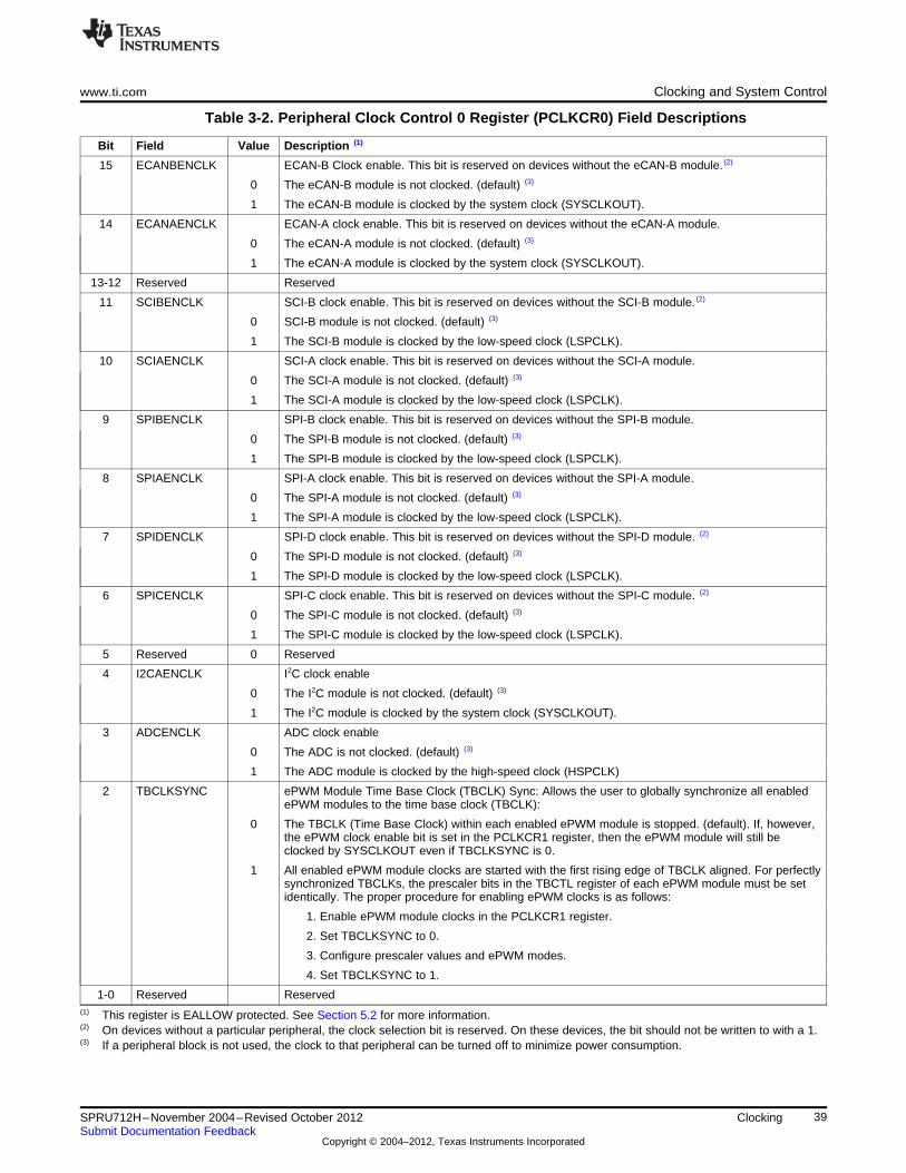
www.ti.com Clocking and System Control
Table 3-2. Peripheral Clock Control 0 Register (PCLKCR0) Field Descriptions
Bit Field Value Description (1)
15 ECANBENCLK ECAN-B Clock enable. This bit is reserved on devices without the eCAN-B module. (2)
0 The eCAN-B module is not clocked. (default) (3)
1 The eCAN-B module is clocked by the system clock (SYSCLKOUT).
14 ECANAENCLK ECAN-A clock enable. This bit is reserved on devices without the eCAN-A module.
0 The eCAN-A module is not clocked. (default) (3)
1 The eCAN-A module is clocked by the system clock (SYSCLKOUT).
13-12 Reserved Reserved
11 SCIBENCLK SCI-B clock enable. This bit is reserved on devices without the SCI-B module. (2)
0 SCI-B module is not clocked. (default) (3)
1 The SCI-B module is clocked by the low-speed clock (LSPCLK).
10 SCIAENCLK SCI-A clock enable. This bit is reserved on devices without the SCI-A module.
0 The SCI-A module is not clocked. (default) (3)
1 The SCI-A module is clocked by the low-speed clock (LSPCLK).
9 SPIBENCLK SPI-B clock enable. This bit is reserved on devices without the SPI-B module.
0 The SPI-B module is not clocked. (default) (3)
1 The SPI-B module is clocked by the low-speed clock (LSPCLK).
8 SPIAENCLK SPI-A clock enable. This bit is reserved on devices without the SPI-A module.
0 The SPI-A module is not clocked. (default) (3)
1 The SPI-A module is clocked by the low-speed clock (LSPCLK).
7 SPIDENCLK SPI-D clock enable. This bit is reserved on devices without the SPI-D module. (2)
0 The SPI-D module is not clocked. (default) (3)
1 The SPI-D module is clocked by the low-speed clock (LSPCLK).
6 SPICENCLK SPI-C clock enable. This bit is reserved on devices without the SPI-C module. (2)
0 The SPI-C module is not clocked. (default) (3)
1 The SPI-C module is clocked by the low-speed clock (LSPCLK).
5 Reserved 0 Reserved
4 I2CAENCLK I2C clock enable
0 The I2C module is not clocked. (default) (3)
1 The I2C module is clocked by the system clock (SYSCLKOUT).
3 ADCENCLK ADC clock enable
0 The ADC is not clocked. (default) (3)
1 The ADC module is clocked by the high-speed clock (HSPCLK)
2 TBCLKSYNC ePWM Module Time Base Clock (TBCLK) Sync: Allows the user to globally synchronize all enabledePWM modules to the time base clock (TBCLK):
0 The TBCLK (Time Base Clock) within each enabled ePWM module is stopped. (default). If, however,the ePWM clock enable bit is set in the PCLKCR1 register, then the ePWM module will still beclocked by SYSCLKOUT even if TBCLKSYNC is 0.
1 All enabled ePWM module clocks are started with the first rising edge of TBCLK aligned. For perfectlysynchronized TBCLKs, the prescaler bits in the TBCTL register of each ePWM module must be setidentically. The proper procedure for enabling ePWM clocks is as follows:
1. Enable ePWM module clocks in the PCLKCR1 register.
2. Set TBCLKSYNC to 0.
3. Configure prescaler values and ePWM modes.
4. Set TBCLKSYNC to 1.
1-0 Reserved Reserved(1) This register is EALLOW protected. See Section 5.2 for more information.(2) On devices without a particular peripheral, the clock selection bit is reserved. On these devices, the bit should not be written to with a 1.(3) If a peripheral block is not used, the clock to that peripheral can be turned off to minimize power consumption.
39SPRU712H–November 2004–Revised October 2012 ClockingSubmit Documentation Feedback
Copyright © 2004–2012, Texas Instruments Incorporated

Clocking and System Control www.ti.com
Figure 3-4. Peripheral Clock Control 1 Register (PCLKCR1)15 14 13 12 11 10 9 8
EQEP2ENCLK EQEP1ENCLK Reserved ECAP4ENCLK ECAP3ENCLK ECAP2ENCLK ECAP1ENCLK
R/W-0 R/W-0 R-0 R/W-0 R/W-0 R/W-0 R/W-0
7 6 5 4 3 2 1 0
EPWM8ENCLK (1) EPWM7ENCLK (1) EPWM6ENCLK EPWM5ENCLK EPWM4ENCLK EPWM3ENCLK EPWM2ENCLK EPWM1ENCLK
R/W-0 R/W-0 R/W-0 R/W-0 R/W-0 R/W-0 R/W-0 R/W-0
LEGEND: R/W = Read/Write; R = Read only; -n = value after reset
(1) Applicable for 28044 device only
Table 3-3. Peripheral Clock Control 1 Register (PCLKCR1) Field Descriptions
Bits Field Value Description (1)
15 EQEP2ENCLK eQEP2 clock enable. This bit is reserved on devices without the eQEP2 module. (2)
0 The eQEP2 module is not clocked. (default) (3)
1 The eQEP2 module is clocked by the system clock (SYSCLKOUT).
14 EQEP1ENCLK eQEP1 clock enable. This bit is reserved on devices without the eQEP1 module.
0 The eQEP1 module is not clocked. (default) (3)
1 The eQEP1 module is clocked by the system clock (SYSCLKOUT).
13-12 Reserved Reserved
11 ECAP4ENCLK eCAP4 clock enable. This bit is reserved devices without the eCAP4 module. (2)
0 The eCAP4 module is not clocked. (default) (3)
1 The eCAP4 module is clocked by the system clock (SYSCLKOUT).
10 ECAP3ENCLK eCAP3 clock enable. This bit is reserved on devices without the eCAP3 module. (2)
0 The eCAP3 module is not clocked. (default) (3)
1 The eCAP3 module is clocked by the system clock (SYSCLKOUT).
9 ECAP2ENCLK eCAP2 clock enable. This bit is reserved on devices without the eCAP2 module.
0 The eCAP2 module is not clocked. (default) (3)
1 The eCAP2 module is clocked by the system clock (SYSCLKOUT).
8 ECAP1ENCLK eCAP1 clock enable. This bit is reserved on devices without the eCAP1 module.
0 The eCAP1 module is not clocked. (default) (3)
1 The eCAP1 module is clocked by the system clock (SYSCLKOUT).
7 EPWM8ENCLK ePWM8 clock enable. (4) This bit is reserved on devices without the ePWM8 module. (2)
0 The ePWM8 module is not clocked. (default) (3)
1 The ePWM8 module is clocked by the system clock (SYSCLKOUT).
6 EPWM7ENCLK ePWM7 clock enable. (4) This bit is reserved on devices without the ePWM7 module. (2)
0 The ePWM7 module is not clocked. (default) (3)
1 The ePWM7 module is clocked by the system clock (SYSCLKOUT).
5 EPWM6ENCLK ePWM6 clock enable. (4) This bit is reserved on devices without the ePWM6 module. (2)
0 The ePWM6 module is not clocked. (default) (3)
1 The ePWM6 module is clocked by the system clock (SYSCLKOUT).
4 EPWM5ENCLK ePWM5 clock enable. (4) This bit is reserved on devices without the ePWM5 module. (2)
0 The ePWM5 module is not clocked. (default) (3)
1 The ePWM5 module is clocked by the system clock (SYSCLKOUT).
3 EPWM4ENCLK ePWM4 clock enable. (4) This bit is reserved on devices without the ePWM4 module. (2)
0 The ePWM4 module is not clocked. (default) (3)
1 The ePWM4 module is clocked by the system clock (SYSCLKOUT).
(1) This register is EALLOW protected. See Section 5.2 for more information.(2) On devices without a particular peripheral, the clock selection bit is reserved. On these devices, the bit should not be written with a value
of 1.(3) If a peripheral block is not used, the clock to that peripheral can be turned off to minimize power consumption.(4) To start the ePWM Time-base clock (TBCLK) within the ePWM modules, the TBCLKSYNC bit in PCLKCR0 must also be set.
40 Clocking SPRU712H–November 2004–Revised October 2012Submit Documentation Feedback
Copyright © 2004–2012, Texas Instruments Incorporated

www.ti.com Clocking and System Control
Table 3-3. Peripheral Clock Control 1 Register (PCLKCR1) Field Descriptions (continued)
Bits Field Value Description (1)
2 EPWM3ENCLK ePWM3 clock enable. (4)
0 The ePWM3 module is not clocked. (default) (3)
1 The ePWM3 module is clocked by the system clock (SYSCLKOUT).
1 EPWM2ENCLK ePWM2 clock enable. (4)
0 The ePWM2 module is not clocked. (default) (3)
1 The ePWM2 module is clocked by the system clock (SYSCLKOUT).
0 EPWM1ENCLK ePWM1 clock enable. (4)
0 The ePWM1 module is not clocked. (default) (3)
1 The ePWM1 module is clocked by the system clock (SYSCLKOUT).
Figure 3-5. Peripheral Clock Control 2 Register (PCLKCR2) (28044)15 8
Reserved
R-0
7 6 5 4 3 2 1 0
EPWM16ENCLK EPWM15ENCLK EPWM14ENCLK EPWM13ENCLK EPWM12ENCLK EPWM11ENCLK EPWM10ENCLK EPWM9ENCLK
R/W-0 R/W-0 R/W-0 R/W-0 R/W-0 R/W-0 R/W-0 R/W-0
LEGEND: R/W = Read/Write; R = Read only; -n = value after reset
Table 3-4. Peripheral Clock Control 2 Register (PCLKCR2) Field Descriptions (28044 only)
Bit Field Value Description
15:8 Reserved Reserved
7 EPWM16ENCLK ePWM module system clock enable
0 Bit cleared by user or reset for low-power operation
1 Enables system clock within the EPWM16 module
6 EPWM15ENCLK ePWM module system clock enable
0 Bit cleared by user or reset for low-power operation
1 Enables system clock within the EPWM15 module
5 EPWM14ENCLK ePWM module system clock enable
0 Bit cleared by user or reset for low-power operation
1 Enables system clock within the EPWM14 module
4 EPWM13ENCLK ePWM module system clock enable
0 Bit cleared by user or reset for low-power operation
1 Enables system clock within the EPWM13 module
3 EPWM12ENCLK ePWM module system clock enable
0 Bit cleared by user or reset for low-power operation
1 Enables system clock within the EPWM12 module
2 EPWM11ENCLK ePWM module system clock enable
0 Bit cleared by user or reset for low-power operation
1 Enables system clock within the EPWM11 module
1 EPWM10ENCLK ePWM module system clock enable
0 Bit cleared by user or reset for low-power operation
1 Enables system clock within the EPWM10 module
0 EPWM9ENCLK ePWM module system clock enable
0 Bit cleared by user or reset for low-power operation
1 Enables system clock within the EPWM9 module
41SPRU712H–November 2004–Revised October 2012 ClockingSubmit Documentation Feedback
Copyright © 2004–2012, Texas Instruments Incorporated
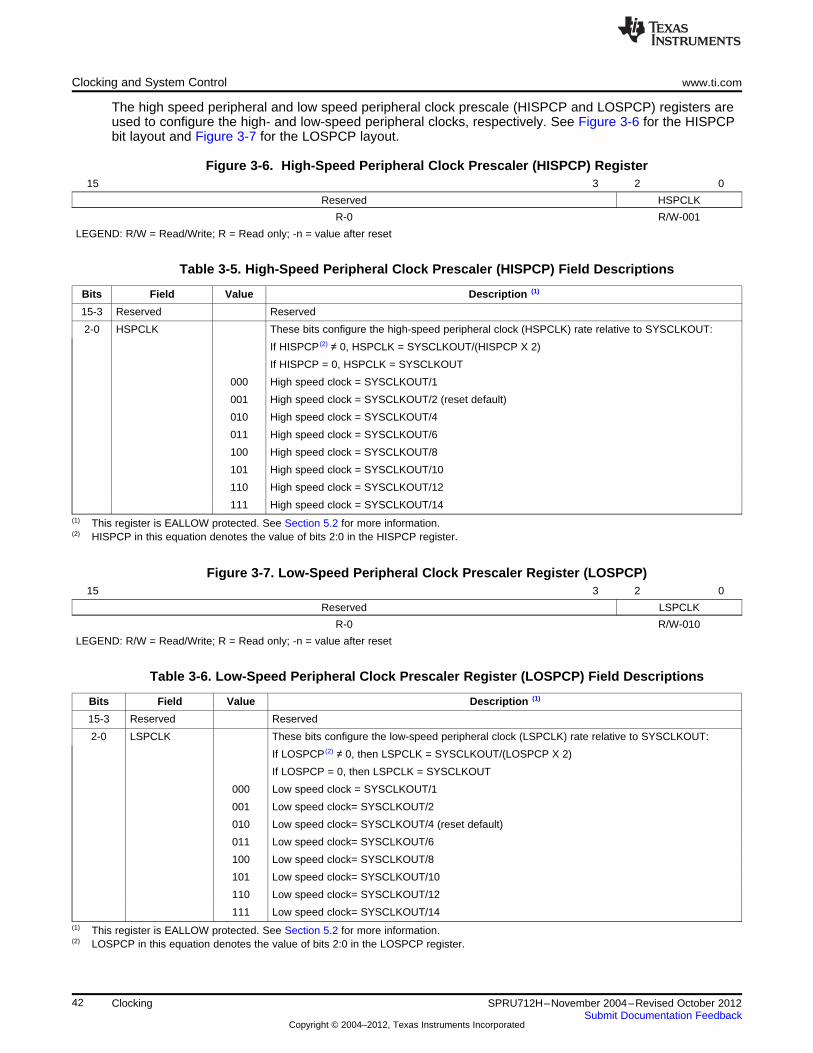
Clocking and System Control www.ti.com
The high speed peripheral and low speed peripheral clock prescale (HISPCP and LOSPCP) registers areused to configure the high- and low-speed peripheral clocks, respectively. See Figure 3-6 for the HISPCPbit layout and Figure 3-7 for the LOSPCP layout.
Figure 3-6. High-Speed Peripheral Clock Prescaler (HISPCP) Register15 3 2 0
Reserved HSPCLK
R-0 R/W-001
LEGEND: R/W = Read/Write; R = Read only; -n = value after reset
Table 3-5. High-Speed Peripheral Clock Prescaler (HISPCP) Field Descriptions
Bits Field Value Description (1)
15-3 Reserved Reserved
2-0 HSPCLK These bits configure the high-speed peripheral clock (HSPCLK) rate relative to SYSCLKOUT:
If HISPCP (2) ≠ 0, HSPCLK = SYSCLKOUT/(HISPCP X 2)
If HISPCP = 0, HSPCLK = SYSCLKOUT
000 High speed clock = SYSCLKOUT/1
001 High speed clock = SYSCLKOUT/2 (reset default)
010 High speed clock = SYSCLKOUT/4
011 High speed clock = SYSCLKOUT/6
100 High speed clock = SYSCLKOUT/8
101 High speed clock = SYSCLKOUT/10
110 High speed clock = SYSCLKOUT/12
111 High speed clock = SYSCLKOUT/14(1) This register is EALLOW protected. See Section 5.2 for more information.(2) HISPCP in this equation denotes the value of bits 2:0 in the HISPCP register.
Figure 3-7. Low-Speed Peripheral Clock Prescaler Register (LOSPCP)15 3 2 0
Reserved LSPCLK
R-0 R/W-010
LEGEND: R/W = Read/Write; R = Read only; -n = value after reset
Table 3-6. Low-Speed Peripheral Clock Prescaler Register (LOSPCP) Field Descriptions
Bits Field Value Description (1)
15-3 Reserved Reserved
2-0 LSPCLK These bits configure the low-speed peripheral clock (LSPCLK) rate relative to SYSCLKOUT:
If LOSPCP (2) ≠ 0, then LSPCLK = SYSCLKOUT/(LOSPCP X 2)
If LOSPCP = 0, then LSPCLK = SYSCLKOUT
000 Low speed clock = SYSCLKOUT/1
001 Low speed clock= SYSCLKOUT/2
010 Low speed clock= SYSCLKOUT/4 (reset default)
011 Low speed clock= SYSCLKOUT/6
100 Low speed clock= SYSCLKOUT/8
101 Low speed clock= SYSCLKOUT/10
110 Low speed clock= SYSCLKOUT/12
111 Low speed clock= SYSCLKOUT/14(1) This register is EALLOW protected. See Section 5.2 for more information.(2) LOSPCP in this equation denotes the value of bits 2:0 in the LOSPCP register.
42 Clocking SPRU712H–November 2004–Revised October 2012Submit Documentation Feedback
Copyright © 2004–2012, Texas Instruments Incorporated

X1
XCLKIN (3.3-V clock input)
On chiposcillator
X2
xor
PLLSTS[OSCOFF]
OSCCLK
PLLVCOCLK
4-bit PLL Select (PLLCR)
OSCCLK or VCOCLK CLKIN
OSCCLK0
PLLSTS[PLLOFF]
n n ≠ 0 /2
PLLSTS[CLKINDIV]
www.ti.com OSC and PLL Block
3.2 OSC and PLL Block
The on-chip oscillator and phase-locked loop (PLL) block provides the clocking signals for the device, aswell as control for low-power mode (LPM) entry.
3.2.1 PLL-Based Clock Module
The 280x devices have an on-chip, PLL-based clock module. The PLL has a 4-bit ratio control to selectdifferent CPU clock rates. Figure 3-8 shows the OSC and PLL block on the 280x.
Figure 3-8. OSC and PLL Block
The PLL-based clock module provides two modes of operation:
• Crystal/Resonator Operation:The on-chip oscillator enables the use of an external crystal/resonator to be attached to the 280xdevices to provide the time base to the device. The crystal/resonator is connected to the X1/X2 pinsand XCLKIN is tied low.
• External clock source operation:If the on-chip oscillator is not used, this mode allows the internal oscillator to be bypassed. The deviceclocks are generated from an external clock source input on either the X1 or the XCLKIN pin.
Option 1: External clock on the XCLKIN pin:When using XCLKIN as the external clock source, you must tie X1 low and leave X2 disconnected. Inthis case, an external oscillator clock is connected to the XCLKIN pin, which allows for a 3.3-V clocksource to be used.
Option 2: External clock on the X1 pin:When using X1 as the clock source, you must tie XCLKIN low and leave X2 disconnected. In this case,an external oscillator clock is connected to the X1 pin, which allows for a 1.8-V clock source to beused.
The OSC circuit enables a crystal to be attached to the 280x devices using the X1 and X2 pins. If a crystalis not used, then an external oscillator can be directly connected to the XCLKIN pin, the X2 pin is leftunconnected, and the X1 pin is tied low. See the TMS320F2809, F2808, F2806, F2802, F2801, C2802,C2801, and F2801x DSPs Data Manual (literature number SPRS230).
Table 3-7. Possible PLL Configuration Modes
PLL Mode Remarks PLLSTS[CLKINDIV] (1) SYSCLKOUT
PLL Off Invoked by the user setting the PLLOFF bit in the PLLSTS register. The 0 OSCCLK/2PLL block is disabled in this mode. This can be useful to reduce system 1 OSCCLKnoise and for low power operation. The PLLCR register must first be setto 0x0000 (PLL Bypass) before entering this mode. The CPU clock(CLKIN) is derived directly from the input clock on either X1/X2, X1 orXCLKIN.
(1) PLLSTS[CLKINDIV] must be 0 before writing to the PLLCR and must only be set to 1 after PLLSTS[PLLLOCKS] = 1. Refer toFigure 3-11.
43SPRU712H–November 2004–Revised October 2012 ClockingSubmit Documentation Feedback
Copyright © 2004–2012, Texas Instruments Incorporated

VCOCLKcounter(13 bits)
Clear ResClear
OSCCLK
Clear
(7 bits)counter
Res Clear
OvfClk
XRS
PLL
Clk Ovf
Off
Clear
OSCCLK
Clockswitchlogic
VCOCLK
C28xCPU
Missingclockreset
PLLCLK/2
PLLSTSreg
PLLCRreg
C28CPU
CLKIN
OSC and PLL Block www.ti.com
Table 3-7. Possible PLL Configuration Modes (continued)
PLL Mode Remarks PLLSTS[CLKINDIV] (1) SYSCLKOUT
PLL Bypass PLL Bypass is the default PLL configuration upon power-up or after an 0 OSCCLK/2external reset (XRS). This mode is selected when the PLLCR register is 1 OSCCLKset to 0x0000 or while the PLL locks to a new frequency after thePLLCR register has been modified. In this mode, the PLL itself isbypassed but the PLL is not turned off.
PLL Enabled Achieved by writing a non-zero value n into the PLLCR register. Upon 0 OSCCLK*n/2writing to the PLLCR, the device will switch to PLL Bypass mode until 1 OSCCLK*nthe PLL locks.
3.2.2 Main Oscillator Fail Detection
Due to vibrations, it is possible for the external clock source to the DSP to become detached and fail toclock the device. When the PLL is not disabled, the main oscillator fail logic allows the device to detectthis condition and default to a known state as described in this section.
Two counters are used to monitor the presence of the OSCCLK signal as shown in Figure 3-9. The firstcounter is incremented by the OSCCLK signal itself either from the X1/X2 or XCLKIN input. When the PLLis not turned off, the second counter is incremented by the VCOCLK coming out of the PLL block. Thesecounters are configured such that when the 7-bit OSCCLK counter overflows, it clears the 13-bit VCOCLKcounter. In normal operating mode, as long as OSCCLK is present, the VCOCLK counter will neveroverflow.
Figure 3-9. Oscillator Fail-Detection Logic Diagram
If the OSCCLK input signal is missing, then the PLL will output a default "limp mode" frequency and theVCOCLK counter will continue to increment. Since the OSCCLK signal is missing, the OSCCLK counterwill not increment and, therefore, the VCOCLK counter is not periodically cleared. Eventually, theVCOCLK counter overflows and, if required, the device switches the CLKIN input to the CPU to the limpmode output frequency of the PLL.
When the VCOCLK counter overflows, the missing clock detection logic resets the CPU, peripherals, andother device logic. The reset generated is known as a missing clock detect logic reset (MCLKRES). TheMCLKRES is an internal reset only. The external XRS pin of the device is not pulled low by MCLKRESand the PLLCR and PLLSTS registers are not reset.
44 Clocking SPRU712H–November 2004–Revised October 2012Submit Documentation Feedback
Copyright © 2004–2012, Texas Instruments Incorporated
www.ti.com OSC and PLL Block
In addition to resetting the device, the missing oscillator logic sets the PLLSTS[MCLKSTS] register bit.When the MCLKCSTS bit is 1, this indicates that the missing oscillator detect logic reset the part and thatthe CPU is now running either at or one-half of the limp mode frequency.
Software should check the PLLSTS[MCLKSTS] bit after a reset to determine if the device was reset byMCLKRES due to a missing clock condition. If MCLKSTS is set, then the firmware should take the actionappropriate for the system such as a system shutdown. The missing clock status can be cleared by writinga 1 to the PLLSTS[MCLKCLR] bit. This will reset the missing clock detection circuits and counters. IfOSCCLK is still missing after writing to the MCLKCLR bit, then the VCOCLK counter again overflows andthe process will repeat.
NOTE: Applications in which the correct CPU operating frequency is absolutely critical shouldimplement a mechanism by which the DSP will be held in reset should the input clocks everfail. For example, an R-C circuit may be used to trigger the XRS pin of the DSP should thecapacitor ever get fully charged. An I/O pin may be used to discharge the capacitor on aperiodic basis to prevent it from getting fully charged. Such a circuit would also help indetecting failure of the flash memory and the VDD3VFL rail.
The following precautions and limitations should be kept in mind:
• Use the proper procedure when changing the PLL Control Register.Always follow the procedure outlined in Figure 3-11 when modifying the PLLCR register.
• Do not write to the PLLCR register when the device is operating in limp mode.When writing to the PLLCR register, the device switches to the CPU's CLKIN input to OSCCLK/2.When operating after limp mode has been detected, OSCCLK may not be present and the clocks tothe system will stop. Always check that the PLLSTS[MCLKSTS] bit = 0 before writing to the PLLCRregister as described in Figure 3-11.
• The watchdog is not functional without an external clock.The watchdog is not functional and cannot generate a reset when OSCCLK is not present. No specialhardware has been added to switch the watchdog to the limp mode clock should OSCCLK becomemissing.
• Limp mode may not work from power up.The PLL may not generate a limp mode clock if OSCCLK is missing from power-up. Only if OSCCLK isinitially present will a limp mode clock be generated by the PLL.
• Do not enter HALT low power mode when the device is operating in limp mode.If you try to enter HALT mode when the device is already operating in limp mode then the device maynot properly enter HALT. The device may instead enter STANDBY mode or may hang and you maynot be able to exit HALT mode. For this reason, always check that the PLLSTS[MCLKSTS] bit = 0before entering HALT mode.
45SPRU712H–November 2004–Revised October 2012 ClockingSubmit Documentation Feedback
Copyright © 2004–2012, Texas Instruments Incorporated

CLKIN
28x CPU
SYSCLKOUT
0,0
0,1
1,0
XCLKOUT Pin
XCLK[XCLKOUTDIV]
1/4
1/2
PLL
PLL BypassOSCCLKX1, X1/X2
orXCLKIN
Default at reset
PLLCR
0
n
n ≠ 0
0
1
1/2
PLLSTS[CLKINDIV]
OSC and PLL Block www.ti.com
The following section describes the behavior of the missing clock detect logic in various operating modes:
• PLL by-pass modeWhen the PLL control register is set to 0x0000, the PLL is by-passed. Depending on the state of thePLLSTS[CLKINDIV] bit either OSCCLK or OSCCLK/2 is connected directly to the CPU's input clock,CLKIN. If the OSCCLK is detected as missing, the device will automatically switch to the PLL, set themissing clock detect status bit, and generate a missing clock reset. The device will now run at the PLLlimp mode frequency or one-half of the PLL limp mode frequency.
• PLL enabled modeWhen the PLL control register is non-zero (PLLCR = n, where n ≠ 0x0000), the PLL is enabled. In thismode, OSCCLK*n/2 or OSCCLK*n is connected to CLKIN of the CPU. If OSCCLK is detected asmissing, the missing clock detect status bit will be set and the device will generate a missing clockreset. The device will now run at one-half of the PLL limp mode frequency.
• STANDBY low power modeIn this mode, the CLKIN to the CPU is stopped. If a missing input clock is detected, the missing clockstatus bit will be set and the device will generate a missing clock reset. If the PLL is in by-pass modewhen this occurs, then one-half of the PLL limp frequency will automatically be routed to the CPU. Thedevice will now run at the PLL limp mode frequency or at one-half of the PLL limp mode frequencydepending on the state of the PLLSTS[CLKINDIV] bit.
• HALT low power modeIn HALT low power mode, all of the clocks to the device are turned off. When the device comes out ofHALT mode, the oscillator and PLL will power up. The counters that are used to detect a missing inputclock (VCOCLK and OSCCLK) will be enabled only after this power-up has completed. If VCOCLKcounter overflows, the missing clock detect status bit will be set and the device will generate a missingclock reset. If the PLL is in by-pass mode when the overflow occurs, then one-half of the PLL limpfrequency will automatically be routed to the CPU. The device will now run at the PLL limp modefrequency or at one-half of the PLL limp mode frequency depending on the state of thePLLSTS[CLKINDIV] bit.
3.2.3 XCLKOUT Generation
The XCLKOUT signal is directly derived from the system clock SYSCLKOUT as shown in Figure 3-10.XCLKOUT can be either equal to, one-half or one-fourth of SYSCLKOUT as determined by theXCLKOUTDIV bits in the XCLK register. By default, at power-up, XCLKOUT = SYSCLKOUT/4 orXCLKOUT = OSCCLK/8.
Figure 3-10. XCLKOUT Generation
The XCLKOUT signal is active when reset is active. Since XCLKOUT should reflect SYSCLKOUT/4 whenreset is low, you can monitor this signal to detect if the device is being properly clocked during debug.There is no internal pullup or pulldown on the XCLKOUT pin.
If XCLKOUT is not being used, it can be turned off by setting the XCLKOUTDIV bits to 1,1 in the XCLKregister.
46 Clocking SPRU712H–November 2004–Revised October 2012Submit Documentation Feedback
Copyright © 2004–2012, Texas Instruments Incorporated

Start
PLLSTS[MCLKSTS]= 1?
Yes
No
Device is operating in limpmode. Take appropriateaction for your system.Do not write to PLLCR.
Set PLL[MCLKOFF] = 0to enable failed oscillator
detect logic.
If required,PLLSTS [CLKINDIV]
can now be changed to 1.
Set new PLLCR value
IsPLLSTS[PLLLOCKS]
= 1?
Continue to wait for PLLto lock. This is importantfor time-critical software.
Set PLLSTS[MCLKOFF] = 1to disable failed oscillator
detect logic
No
Yes
PLLSTS[CLKINDIV]= 1?
No
Set PLLSTS[CLKINDIV] = 0Yes
www.ti.com OSC and PLL Block
3.2.4 PLL Control (PLLCR) Register
The PLLCR register is used to change the PLL multiplier of the device using the procedure shown inFigure 3-11.
Figure 3-11. PLLCR Change Procedure Flow Chart
Before writing to the PLLCR register, the following two requirements must be met:
1. The PLLSTS[CLKINDIV] bit must be 0 (CLKIN divide by 2 enabled). Only change PLLSTS[CLKINDIV]to 1 after the PLL has completed locking, i.e., after PLLSTS[PLLLOCKS] = 1.
2. The device must not be operating in "limp mode". That is, the PLLSTS[MCLKSTS] bit must be 0.
47SPRU712H–November 2004–Revised October 2012 ClockingSubmit Documentation Feedback
Copyright © 2004–2012, Texas Instruments Incorporated

OSC and PLL Block www.ti.com
When the CPU writes to the PLLCR[DIV] bits, the PLL logic switches the CPU clock (CLKIN) toOSCCLK/2. Once the PLL is stable and has locked at the new specified frequency, the PLL switchesCLKIN to the new value as shown in Table 3-8. When this happens, the PLLLOCKS bit in the PLLSTSregister is set, indicating that the PLL has finished locking and the device is now running at the newfrequency. User software can monitor the PLLLOCKS bit to determine when the PLL has completedlocking. Once PLLSTS[PLLLOCKS] = 1, CLKINDIV can be changed to 1 to disable the CLKIN divide by 2if desired.
Follow the procedure in Figure 3-11 any time you are writing to the PLLCR register.
3.2.5 PLL Control, Status and XCLKOUT Register Descriptions
The DIV field in the PLLCR register controls whether the PLL is bypassed or not and sets the PLLclocking ratio when it is not bypassed. PLL bypass is the default mode after reset. Do not write to the DIVfield if the PLLSTS[CLKINDIV] bit is set, or if the PLL is operating in limp mode as indicated by thePLLSTS[MCLKSTS] bit being set. See the procedure for changing the PLLCR described in Figure 3-11.
Figure 3-12. PLLCR Register Layout15 4 3 0
Reserved DIV
R-0 R/W-0
LEGEND: R/W = Read/Write; R = Read only; -n = value after reset
Table 3-8. PLLCR Bit Descriptions
SYSCLKOUT (CLKIN) (1)
PLLCR[DIV] Value (2) PLLSTS[CLKINDIV] = 0 (3) PLLSTS[CLKINDIV] = 1 (3)
0000 (PLL bypass) OSCCLK/2 (Default) (4) OSCCLK
0001 (OSCCLK*1)/2 OSCCLK*1
0010 (OSCCLK*2)/2 OSCCLK*2
0011 (OSCCLK*3)/2 OSCCLK*3
0100 (OSCCLK*4)/2 OSCCLK*4
0101 (OSCCLK*5)/2 OSCCLK*5
0110 (OSCCLK*6)/2 OSCCLK*6
0111 (OSCCLK*7)/2 OSCCLK*7
1000 (OSCCLK*8)/2 OSCCLK*8
1001 (OSCCLK*9)/2 OSCCLK*9
1010 (OSCCLK*10)/2 OSCCLK*10
1011 - 1111 reserved reserved(1) This register is EALLOW protected. See Section 5.2 for more information.(2) CLKIN is the input clock to the CPU. SYSCLKOUT is the output clock from the CPU. The frequency of SYSCLKOUT is the same
as CLKIN.(3) PLLSTS[CLKINDIV] must be 0 before writing to the PLLCR and must only be set to 1 after PLLSTS[PLLLOCKS] = 1. Refer to
Figure 3-11.(4) The PLL control register (PLLCR) and PLL Status Register (PLLSTS) are reset to their default state by the XRS signal or a
watchdog reset only. A reset issued by the debugger or the missing clock detect logic have no effect.
Figure 3-13. PLL Status Register (PLLSTS)15 8
Reserved
R-0
7 6 5 4 3 2 1 0
Reserved MCLKOFF OSCOFF MCLKCLR MCLKSTS PLLOFF CLKINDIV PLLLOCKS
R-0 R/W-0 R/W-0 R=0/W-0 R-0 R/W-0 R/W-0 R-1
LEGEND: R/W = Read/Write; R = Read only; -n = value after reset
48 Clocking SPRU712H–November 2004–Revised October 2012Submit Documentation Feedback
Copyright © 2004–2012, Texas Instruments Incorporated

www.ti.com OSC and PLL Block
Table 3-9. PLL Status Register (PLLSTS) Field Descriptions
Bits Field Value Description (1) (2)
15-7 Reserved Reserved
6 MCLKOFF Missing clock-detect off bit
0 Main oscillator fail-detect logic is enabled. (default)
1 Main oscillator fail-detect logic is disabled and the PLL will not issue a limp-mode clock. Usethis mode when code must not be affected by the detection circuit. For example, if externalclocks are turned off.
5 OSCOFF Oscillator Clock Off Bit
0 The OSCCLK signal from X1, X1/X2 or XCLKIN is fed to the PLL block. (default)
1 The OSCCLK signal from X1, X1/X2 or XCLKIN is not fed to the PLL block. This does not shutdown the internal oscillator. The OSCOFF bit is used for testing the missing clock detectionlogic.
When the OSCOFF bit is set, do not enter HALT or STANDBY modes or write to PLLCR asthese operations can result in unpredictable behavior.
When the OSCOFF bit is set, the behavior of the watchdog is different depending on whichinput clock source (X1, X1/X2 or XCLKIN) is being used:
• X1 or X1/X2: The watchdog is not functional.• XCLKIN: The watchdog is functional and should be disabled before setting OSCOFF.
4 MCLKCLR Missing Clock Clear Bit.
0 Writing a 0 has no effect. This bit always reads 0.
1 Forces the missing clock detection circuits to be cleared and reset. If OSCCLK is still missing,the detection circuit will again generate a reset to the system, set the missing clock status bit(MCLKSTS), and the CPU will be powered by the PLL operating at a "limp mode" frequency.
3 MCLKSTS Missing Clock Status Bit. Check the status of this bit after a reset to determine whether amissing oscillator condition was detected. Under normal conditions, this bit should be 0. Writesto this bit are ignored. This bit will be cleared by writing to the MCLKCLR bit or by forcing anexternal reset.
0 Indicates normal operation. A missing clock condition has not been detected.
1 Indicates that OSCCLK was detected as missing. The main oscillator fail detect logic has resetthe device and the CPU is now clocked by the PLL operating at the limp mode frequency.
2 PLLOFF PLL Off Bit. This bit turns off the PLL. This is useful for system noise testing. This mode mustonly be used when the PLLCR register is set to 0x0000.
0 PLL On (default)
1 PLL Off. While the PLLOFF bit is set the PLL module will be kept powered down.
The device must be in PLL bypass mode (PLLCR = 0x0000) before writing a 1 to PLLOFF.While the PLL is turned off (PLLOFF = 1), do not write a non-zero value to the PLLCR.
The STANDBY and HALT low power modes will work as expected when PLLOFF = 1. Afterwaking up from HALT or STANDBY the PLL module will remain powered down.
1 CLKINDIV Clock Divide By 2 Enable or Disable: The divide-by-2 for the CLKIN signal into the CPU can beenabled or disabled by this bit. CLKINDIV must be 0 before writing to PLLCR and must only beset after PLLLOCKS = 1. Refer to Figure 3-11.
0 CLKIN divide by 2 is enabled (default). CLKINDIV must be set to 0 before writing to PLLCR.
1 CLKIN divide by 2 is disabled. Only change CLKINDIV to 1 after PLLLOCKS = 1.
0 PLLLOCKS PLL Lock Status Bit
0 Indicates that the PLLCR register has been written to and the PLL is currently locking. The CPUis clocked by OSCCLK/2 until the PLL locks.
1 Indicates that the PLL has finished locking and is now stable.(1) This register is reset to its default state only by the XRS signal or a watchdog reset. It is not reset by a missing clock or debugger reset.(2) This register is EALLOW protected. See Section 5.2 for more information.
49SPRU712H–November 2004–Revised October 2012 ClockingSubmit Documentation Feedback
Copyright © 2004–2012, Texas Instruments Incorporated

Low-Power Modes Block www.ti.com
Figure 3-14. XCLKOUT Register (XCLK)15 12 11 8
XCLKINCNT X1CNT
R/W-0 R/W-0
7 5 4 3 2 1 0
Reserved XCLKINDAT X1DAT XCLKOUTDAT XCLKOUTDIV
R-0 W-0 R-0 R-0 R/W-0
LEGEND: R/W = Read/Write; R = Read only; -n = value after reset
Table 3-10. XCLKOUT Register (XCLK) Field Descriptions
Bit Field Value Description (1)
15-12 XCLKINCNT This bit is reserved for Texas Instruments use only.
11-8 X1CNT This bit is reserved for Texas Instruments use only.
7-5 Reserved
4 XCLKINDAT This bit is reserved for Texas Instruments use only.
3 X1DAT This bit is reserved for Texas Instruments use only.
2 XCLKOUTDAT This bit is reserved for Texas Instruments use only.
1 XCLKOUTDIV XCLKOUT Divide Ratio. These two bits select the XCLKOUT frequency ratio relative toSYSCLKOUT. The ratios are:
00 XCLKOUT = SYSCLKOUT/4 (default)
01 XCLKOUT = SYSCLKOUT/2
10 XCLKOUT = SYSCLKOUT
11 XCLKOUT = Off (pin in high-impedance mode)(1) This register is EALLOW protected. See Section 5.2 for more information.
3.2.6 External Reference Oscillator Clock Option
TI recommends that customers have the resonator/crystal vendor characterize the operation of theirdevice with the DSP chip. The resonator/crystal vendor has the equipment and expertise to tune the tankcircuit. The vendor can also advise the customer regarding the proper tank component values to provideproper start-up and stability over the entire operating range.
3.3 Low-Power Modes Block
The low-power modes on the 280x devices are similar to the 240x devices. Table 3-11 summarizes thevarious modes.
The various low-power modes operate as shown in Table 3-12.
See the TMS320F2809, F2808, F2806, F2802, F2801, C2802, C2801, and F2801x DSPs Data Manual(literature number SPRS230) for exact timing for entering and exiting the low power modes.
Table 3-11. 280x Low-Power Modes
Mode LPMCR0[1:0] OSCCLK CLKIN SYSCLKOUT Exit (1)
IDLE 00 On On On (2) XRS,Watchdog interrupt,Any enabled interrupt,XNMI
(1) The Exit column lists which signals or under what conditions the low power mode is exited. This signal must be kept low long enough foran interrupt to be recognized by the device. Otherwise the IDLE mode is not exited and the device goes back into the indicated lowpower mode.
(2) The IDLE mode on the 28x behaves differently than on the 24x/240x. On the 28x, the clock output from the CPU (SYSCLKOUT) is stillfunctional while on the 24x/240x the clock is turned off.
50 Clocking SPRU712H–November 2004–Revised October 2012Submit Documentation Feedback
Copyright © 2004–2012, Texas Instruments Incorporated

www.ti.com Low-Power Modes Block
Table 3-11. 280x Low-Power Modes (continued)
Mode LPMCR0[1:0] OSCCLK CLKIN SYSCLKOUT Exit (1)
STANDBY 01 On Off Off XRS,(watchdog still running) Watchdog interrupt,
GPIO Port A signal,Debugger (3)
HALT 1X Off Off Off XRS,(oscillator and PLL turned off, GPIO Port A Signal,
watchdog not functional) Debugger (3)
(3) On the 28x, the JTAG port can still function even if the clock to the CPU (CLKIN) is turned off.
Table 3-12. Low Power Modes
Mode Description
IDLE This mode is exited by any enabled interrupt or an NMI. The LPM block itself performs no tasks during this mode.Mode:
STANDBY If the LPM bits in the LPMCR0 register are set to 01, the device enters STANDBY mode when the IDLE instruction isMode: executed. In STANDBY mode the clock input to the CPU (CLKIN) is disabled, which disables all clocks derived from
SYSCLKOUT. The oscillator and PLL and watchdog will still function. Before entering the STANDBY mode, you shouldperform the following tasks:
• Enable the WAKEINT interrupt in the PIE module. This interrupt is connected to both the watchdog and the lowpower mode module interrupt.
• If desired, specify one of the GPIO port A signals to wake the device in the GPIOLPMSEL register. TheGPIOLPMSEL register is part of the GPIO module. In addition to the selected GPIO signal, the XRS input and thewatchdog interrupt, if enabled in the LPMCRO register, can wake the device from the STANDBY mode.
• Select the input qualification in the LPMCR0 register for the signal that will wake the device.
When the selected external signal goes low, it must remain low a number of OSCCLK cycles as specified by thequalification period in the LPMCR0 register. If the signal should be sampled high during this time, the qualification willrestart. At the end of the qualification period, the PLL enables the CLKIN to the CPU and the WAKEINT interrupt islatched in the PIE block. The CPU then responds to the WAKEINT interrupt if it is enabled.
HALT If the LPM bits in the LPMCR0 register are set to 1x, the device enters the HALT mode when the IDLE instruction isMode: executed. In HALT mode all of the device clocks, including the PLL and oscillator, are shut down. Before entering the
HALT mode, you should perform the following tasks:• Enable the WAKEINT interrupt in the PIE module (PIEIER1.8 = 1). This interrupt is connected to both the
watchdog and the Low-Power-Mode module interrupt.• Specify one of the GPIO port A signals to wake the device in the GPIOLPMSEL register. The GPIOLPMSEL
register is part of the GPIO module. In addition to the selected GPIO signal, the XRS input can also wake thedevice from the HALT mode.
• Disable all interrupts with the possible exception of the HALT mode wakeup interrupt. The interrupts can be re-enabled after the device is brought out of HALT mode.
1. For device to exit HALT mode properly, the following conditions must be met:
Bit 7 (INT1.8) of PIEIER1 register should be 1.
Bit 0 (INT1) of IER register must be 1.2. If the above conditions are met,
(a) WAKE_INT ISR will be executed first, followed by the instruction(s) after IDLE, if INTM =0.
(b) WAKE_INT ISR will not be executed and instruction(s) after IDLE will be executed, ifINTM = 1.
Do not enter HALT low power mode when the device is operating in limp mode (PLLSTS[MCLKSTS] = 1).If you try to enter HALT mode when the device is already operating in limp mode then the device may not properly enterHALT. The device may instead enter STANDBY mode or may hang and you may not be able to exit HALT mode. Forthis reason, always check that the PLLSTS[MCLKSTS] bit = 0 before entering HALT mode.
When the selected external signal goes low, it is fed asynchronously to the LPM block. The oscillator is turned on andbegins to power up. You must hold the signal low long enough for the oscillator to complete power up. Once theoscillator has stabilized, the PLL lock sequence is initiated. Once the PLL has locked, it feeds the CLKIN to the CPU atwhich time the CPU responds to the WAKEINT interrupt if enabled.
51SPRU712H–November 2004–Revised October 2012 ClockingSubmit Documentation Feedback
Copyright © 2004–2012, Texas Instruments Incorporated

Low-Power Modes Block www.ti.com
The low-power modes are controlled by the LPMCR0 register (Figure 3-15).
NOTE: The GPIO35 signal is internally available, but not pinned out. The internal pullup for thissignal is disabled upon reset. To minimize the leakage currents in order to ensure that thelow-power mode IDDIO current stays within the datasheet limits, this pullup has to beenabled in the GPBPUD register.
Figure 3-15. Low Power Mode Control 0 Register (LPMCR0)15 14 8 7 2 1 0
WDINTE Reserved QUALSTDBY LPM
R/W-0 R-0 R/W-1 R/W-0
LEGEND: R/W = Read/Write; R = Read only; -n = value after reset
Table 3-13. Low Power Mode Control 0 Register (LPMCR0) Field Descriptions
Bits Field Value Description (1)
15 WDINTE Watchdog interrupt enable
0 The watchdog interrupt is not allowed to wake the device from STANDBY. (default)
The watchdog is allowed to wake the device from STANDBY. The watchdog interrupt must also1 be enabled in the SCSR Register.
14-8 Reserved Reserved
7-2 QUALSTDBY Select number of OSCCLK clock cycles to qualify the selected GPIO inputs that wake the devicefrom STANDBY mode. This qualification is only used when in STANDBY mode. The GPIOsignals that can wake the device from STANDBY are specified in the GPIOLPMSEL register.
000000 2 OSCCLKs (default)
000001 3 OSCCLKs
. . . . . .
111111 65 OSCCLKs
1-0 LPM (2) These bits set the low power mode for the device.
00 Set the low power mode to IDLE (default)
01 Set the low power mode to STANDBY
10 Set the low power mode to HALT (3)
11 Set the low power mode to HALT (3)
(1) This register is EALLOW protected. See Section 5.2 for more information.(2) The low power mode bits (LPM) only take effect when the IDLE instruction is executed. Therefore, you must set the LPM bits to the
appropriate mode before executing the IDLE instruction.(3) If you try to enter HALT mode when the device is already operating in limp mode then the device may not properly enter HALT. The
device may instead enter STANDBY mode or may hang and you may not be able to exit HALT mode. For this reason, always check thatthe PLLSTS[MCLKSTS] bit = 0 before entering HALT mode.
52 Clocking SPRU712H–November 2004–Revised October 2012Submit Documentation Feedback
Copyright © 2004–2012, Texas Instruments Incorporated
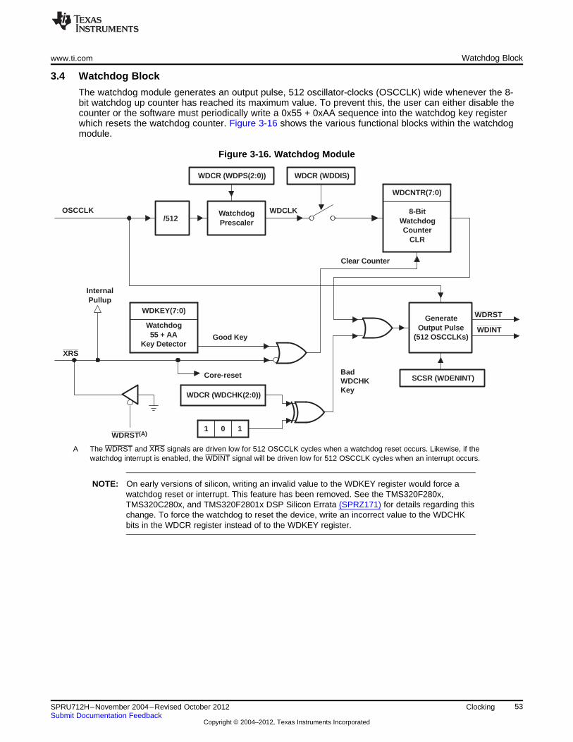
/512OSCCLK
WDCR (WDPS(2:0))
WDCLK
WDCNTR(7:0)
WDKEY(7:0)
Good Key
1 0 1
WDCR (WDCHK(2:0))
BadWDCHKKey
WDCR (WDDIS)
Clear Counter
SCSR (WDENINT)
WatchdogPrescaler
GenerateOutput Pulse
(512 OSCCLKs)
8-BitWatchdogCounter
CLR
WDRST
WDINTWatchdog55 + AA
Key DetectorXRS
Core-reset
WDRST(A)
InternalPullup
www.ti.com Watchdog Block
3.4 Watchdog Block
The watchdog module generates an output pulse, 512 oscillator-clocks (OSCCLK) wide whenever the 8-bit watchdog up counter has reached its maximum value. To prevent this, the user can either disable thecounter or the software must periodically write a 0x55 + 0xAA sequence into the watchdog key registerwhich resets the watchdog counter. Figure 3-16 shows the various functional blocks within the watchdogmodule.
Figure 3-16. Watchdog Module
A The WDRST and XRS signals are driven low for 512 OSCCLK cycles when a watchdog reset occurs. Likewise, if thewatchdog interrupt is enabled, the WDINT signal will be driven low for 512 OSCCLK cycles when an interrupt occurs.
NOTE: On early versions of silicon, writing an invalid value to the WDKEY register would force awatchdog reset or interrupt. This feature has been removed. See the TMS320F280x,TMS320C280x, and TMS320F2801x DSP Silicon Errata (SPRZ171) for details regarding thischange. To force the watchdog to reset the device, write an incorrect value to the WDCHKbits in the WDCR register instead of to the WDKEY register.
53SPRU712H–November 2004–Revised October 2012 ClockingSubmit Documentation Feedback
Copyright © 2004–2012, Texas Instruments Incorporated

Watchdog Block www.ti.com
3.4.1 Servicing The Watchdog Timer
The WDCNTR is reset when the proper sequence is written to the WDKEY register before the 8-bitwatchdog counter (WDCNTR) overflows. The WDCNTR is reset-enabled when a value of 0x55 is writtento the WDKEY. When the next value written to the WDKEY register is 0xAA, the WDCNTR is reset. Only awrite of 0x55 followed by a write of 0xAA to the WDKEY resets the WDCNTR. Any other sequence orvalues are not effective.
Table 3-14. Example Watchdog Key Sequences
Step Value Written to WDKEY Result
1 0xAA No action
2 0xAA No action
3 0x55 WDCNTR is enabled to be reset if next value is 0xAA.
4 0x55 WDCNTR is enabled to be reset if next value is 0xAA.
5 0x55 WDCNTR is enabled to be reset if next value is 0xAA.
6 0xAA WDCNTR is reset.
7 0xAA No action
8 0x55 WDCNTR is enabled to be reset if next value is 0xAA.
9 0xAA WDCNTR is reset.
10 0x55 WDCNTR is enabled to be reset if next value is 0xAA.
11 0x32 Improper value written to WDKEY.No action, WDCNTR no longer enabled to be reset by next0xAA.
12 0xAA No action due to previous invalid value.
13 0x55 WDCNTR is enabled to be reset if next value is 0xAA.
14 0xAA WDCNTR is reset.
Step 3 in Table 3-14 is the first action that enables the WDCNTR to be reset. The WDCNTR is notactually reset until step 6. Step 8 again re-enables the WDCNTR to be reset and step 9 resets theWDCNTR. Step 10 again re-enables the WDCNTR ro be reset. Writing the wrong key value to theWDKEY in step 11 causes no action, however the WDCNTR is no longer enabled to be reset and the0xAA in step 12 now has no effect.
If the watchdog is configured to reset the device, then a WDCR overflow or writing the incorrect value tothe WDCR[WDCHK] bits resets the device and sets the watchdog flag (WDFLAG) in the WDCR register.After a reset, the program can read the state of this flag to determine the source of the reset. After reset,the WDFLAG should be cleared by software to allow the source of subsequent resets to be determined.Watchdog resets are not prevented when the flag is set.
3.4.2 Watchdog Reset or Watchdog Interrupt Mode
The watchdog can be configured in the SCSR register to either reset the device (WDRST) or assert aninterrupt (WDINT) if the watchdog counter reaches its maximum value. The behavior of each condition isdescribed below:
• Reset mode:If the watchdog is configured to reset the device, then the WDRST signal pulls the device reset (XRS)pin low for 512 OSCCLK cycles when the watchdog counter reaches its maximum value.
• Interrupt mode:If the watchdog is configured to assert an interrupt, the WDINT signal is driven low for 512 OSCCLKcycles, causing the WAKEINT interrupt in the PIE to be taken if it is enabled in the PIE module. Thewatchdog interrupt is edge triggered on the falling edge of WDINT. Thus, if the WAKEINT interrupt isre-enabled before WDINT goes inactive, you will not immediately get another interrupt. The nextWAKEINT interrupt will occur at the next watchdog timeout.
If the watchdog is re-configured from interrupt mode to reset mode while WDINT is still active low, thedevice resets immediately. The WDINTS bit in the SCSR register can be read to determine the currentstate of the WDINT signal before reconfiguring the watchdog to reset mode.
54 Clocking SPRU712H–November 2004–Revised October 2012Submit Documentation Feedback
Copyright © 2004–2012, Texas Instruments Incorporated

www.ti.com Watchdog Block
3.4.3 Watchdog Operation in Low Power Modes
In STANDBY mode, all of the clocks to the peripherals are turned off on the device. The only peripheralthat remains functional is the watchdog since the watchdog module runs off the oscillator clock(OSCCLK). The WDINT signal is fed to the Low Power Modes (LPM) block so that it can be used to wakethe device from STANDBY low power mode (if enabled). See the Low Power Modes Block section of thedevice data manual for details.
In IDLE mode, the watchdog interrupt (WDINT) signal can generate an interrupt to the CPU to take theCPU out of IDLE mode. The watchdog is connected to the WAKEINT interrupt in the PIE.
NOTE: If the watchdog interrupt is used to wake-up from an IDLE or STANDBY low power modecondition, then the WDINT signal must go high again before attempting to go back into theIDLE or STANDBY mode. The WDINT signal is held low for 512 OSCCLK cycles when thewatchdog interrupt is generated. You can determine the current state of WDINT by readingthe watchdog interrupt status bit (WDINTS) bit in the SCSR register. WDINTS follows thestate of WDINT by two SYSCLKOUT cycles.
In HALT mode, this feature cannot be used because the oscillator (and PLL) are turned off and, therefore,so is the watchdog.
3.4.4 Emulation Considerations
The watchdog module behaves as follows under various debug conditions:
CPU Suspended: When the CPU is suspended, the watchdog clock (WDCLK) is suspendedRun-Free Mode: When the CPU is placed in run-free mode, then the watchdog module
resumes operation as normal.Real-Time Single-Step When the CPU is in real-time single-step mode, the watchdog clockMode: (WDCLK) is suspended. The watchdog remains suspended even within real-
time interrupts.Real-Time Run-Free When the CPU is in real-time run-free mode, the watchdog operates asMode: normal.
55SPRU712H–November 2004–Revised October 2012 ClockingSubmit Documentation Feedback
Copyright © 2004–2012, Texas Instruments Incorporated
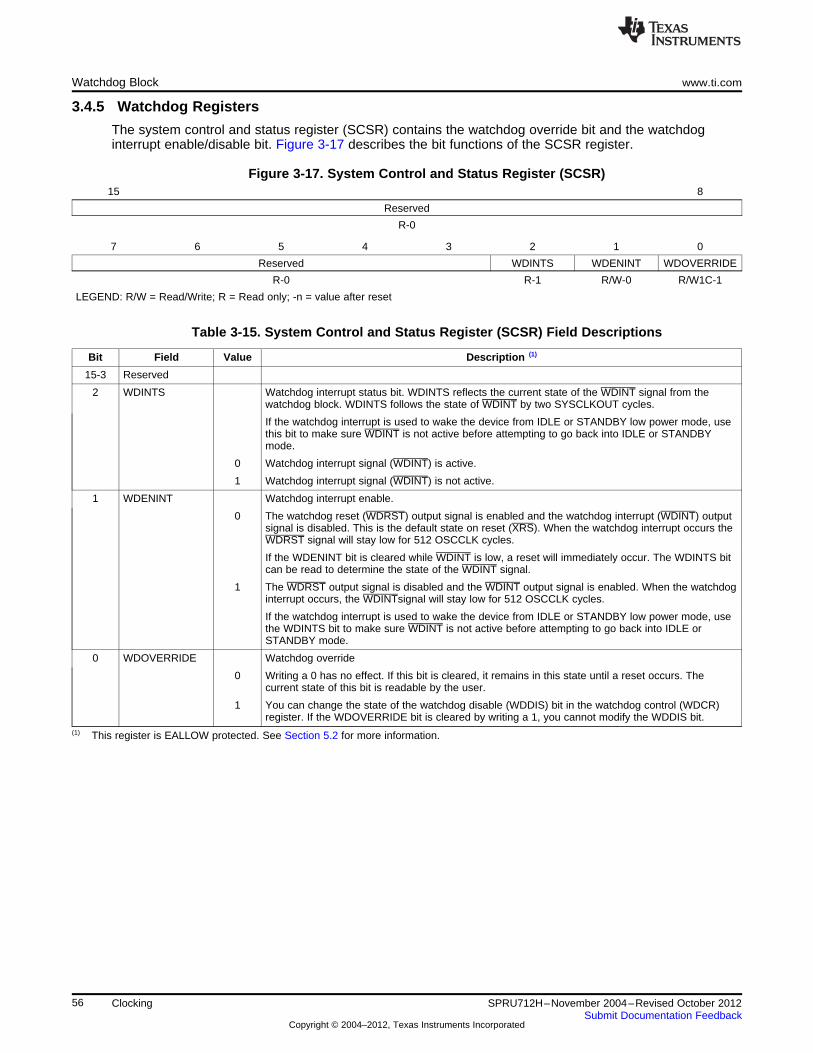
Watchdog Block www.ti.com
3.4.5 Watchdog Registers
The system control and status register (SCSR) contains the watchdog override bit and the watchdoginterrupt enable/disable bit. Figure 3-17 describes the bit functions of the SCSR register.
Figure 3-17. System Control and Status Register (SCSR)15 8
Reserved
R-0
7 6 5 4 3 2 1 0
Reserved WDINTS WDENINT WDOVERRIDE
R-0 R-1 R/W-0 R/W1C-1
LEGEND: R/W = Read/Write; R = Read only; -n = value after reset
Table 3-15. System Control and Status Register (SCSR) Field Descriptions
Bit Field Value Description (1)
15-3 Reserved
2 WDINTS Watchdog interrupt status bit. WDINTS reflects the current state of the WDINT signal from thewatchdog block. WDINTS follows the state of WDINT by two SYSCLKOUT cycles.
If the watchdog interrupt is used to wake the device from IDLE or STANDBY low power mode, usethis bit to make sure WDINT is not active before attempting to go back into IDLE or STANDBYmode.
0 Watchdog interrupt signal (WDINT) is active.
1 Watchdog interrupt signal (WDINT) is not active.
1 WDENINT Watchdog interrupt enable.
0 The watchdog reset (WDRST) output signal is enabled and the watchdog interrupt (WDINT) outputsignal is disabled. This is the default state on reset (XRS). When the watchdog interrupt occurs theWDRST signal will stay low for 512 OSCCLK cycles.
If the WDENINT bit is cleared while WDINT is low, a reset will immediately occur. The WDINTS bitcan be read to determine the state of the WDINT signal.
1 The WDRST output signal is disabled and the WDINT output signal is enabled. When the watchdoginterrupt occurs, the WDINTsignal will stay low for 512 OSCCLK cycles.
If the watchdog interrupt is used to wake the device from IDLE or STANDBY low power mode, usethe WDINTS bit to make sure WDINT is not active before attempting to go back into IDLE orSTANDBY mode.
0 WDOVERRIDE Watchdog override
0 Writing a 0 has no effect. If this bit is cleared, it remains in this state until a reset occurs. Thecurrent state of this bit is readable by the user.
1 You can change the state of the watchdog disable (WDDIS) bit in the watchdog control (WDCR)register. If the WDOVERRIDE bit is cleared by writing a 1, you cannot modify the WDDIS bit.
(1) This register is EALLOW protected. See Section 5.2 for more information.
56 Clocking SPRU712H–November 2004–Revised October 2012Submit Documentation Feedback
Copyright © 2004–2012, Texas Instruments Incorporated

www.ti.com Watchdog Block
Figure 3-18. Watchdog Counter Register (WDCNTR)15 8 7 0
Reserved WDCNTR
R-0 R-0
LEGEND: R/W = Read/Write; R = Read only; -n = value after reset
Table 3-16. Watchdog Counter Register (WDCNTR) Field Descriptions
Bits Field Description
15-8 Reserved Reserved
7-0 WDCNTR These bits contain the current value of the WD counter. The 8-bit counter continually increments at thewatchdog clock (WDCLK), rate. If the counter overflows, then the watchdog initiates a reset. If the WDKEYregister is written with a valid combination, then the counter is reset to zero. The watchdog clock rate isconfigured in the WDCR register.
Figure 3-19. Watchdog Reset Key Register (WDKEY)15 8 7 0
Reserved WDKEY
R-0 R/W-0
LEGEND: R/W = Read/Write; R = Read only; -n = value after reset
Table 3-17. Watchdog Reset Key Register (WDKEY) Field Descriptions
Bits Field Value Description (1)
15-8 Reserved Reserved
7-0 WDKEY Refer to Table 3-14 for examples of different WDKEY write sequences.
0x55 + Writing 0x55 followed by 0xAA to WDKEY causes the WDCNTR bits to be cleared.0xAA
Other Writing any value other than 0x55 or 0xAA causes no action to be generated. If any value other thanvalue 0xAA is written after 0x55, then the sequence must restart with 0x55.
Reads from WDKEY return the value of the WDCR register.(1) This register is EALLOW protected. See Section 5.2 for more information.
Figure 3-20. Watchdog Control Register (WDCR)15 8
Reserved
7 6 5 3 2 0
WDFLAG WDDIS WDCHK WDPS
R/W1C-0 R/W-0 R/W-0 R/W-0
LEGEND: R/W = Read/Write; R = Read only; -n = value after reset
Table 3-18. Watchdog Control Register (WDCR) Field Descriptions
Bits Field Value Description (1)
15-8 Reserved Reserved
7 WDFLAG Watchdog reset status flag bit
0 The reset was caused either by the XRS pin or because of power-up. The bit remains latcheduntil you write a 1 to clear the condition. Writes of 0 are ignored.
1 Indicates a watchdog reset (WDRST) generated the reset condition. .
6 WDDIS Watchdog disable. On reset, the watchdog module is enabled.
0 Enables the watchdog module. WDDIS can be modified only if the WDOVERRIDE bit in theSCSR register is set to 1. (default)
1 Disables the watchdog module.
(1) This register is EALLOW protected. See Section 5.2 for more information.
57SPRU712H–November 2004–Revised October 2012 ClockingSubmit Documentation Feedback
Copyright © 2004–2012, Texas Instruments Incorporated

Borrow
Reset
Timer reload
SYSCLKOUTTCR.4
(Timer start status)
TINT
16-bit timer divide-down TDDRH:TDDR
32-bit timer periodPRDH:PRD
32-bit counterTIMH:TIM
16-bit prescale counterPSCH:PSC
Borrow
32-Bit CPU Timers 0/1/2 www.ti.com
Table 3-18. Watchdog Control Register (WDCR) Field Descriptions (continued)
Bits Field Value Description (1)
5-3 WDCHK Watchdog check.
0,0,0 You must ALWAYS write 1,0,1 to these bits whenever a write to this register is performedunless the intent is to reset the device via software.
other If the watchdog is enabled, then writing any other value causes an immediate device reset orwatchdog interrupt to be taken. These three bits always read back as zero (0, 0, 0). Thisfeature can be used to generate a software reset of the DSP.
2-0 WDPS Watchdog pre-scale. These bits configure the watchdog counter clock (WDCLK) rate relativeto OSCCLK/512:
000 WDCLK = OSCCLK/512/1 (default)
001 WDCLK = OSCCLK/512/1
010 WDCLK = OSCCLK/512/2
011 WDCLK = OSCCLK/512/4
100 WDCLK = OSCCLK/512/8
101 WDCLK = OSCCLK/512/16
110 WDCLK = OSCCLK/512/32
111 WDCLK = OSCCLK/512/64
When the XRS line is low, the WDFLAG bit is forced low. The WDFLAG bit is only set if a rising edge onWDRST signal is detected (after synch and an 8192 SYSCLKOUT cycle delay) and the XRS signal ishigh. If the XRS signal is low when WDRST goes high, then the WDFLAG bit remains at 0. In a typicalapplication, the WDRST signal connects to the XRS input. Hence to distinguish between a watchdog resetand an external device reset, an external reset must be longer in duration then the watchdog pulse.
3.5 32-Bit CPU Timers 0/1/2
This section describes the three 32-bit CPU-timers (Figure 3-21) (TIMER0/1/2).
CPU-Timers 0 and 1 can be used in user applications. CPU-Timer 2 is reserved for DSP-BIOS. If theapplication is not using DSP-BIOS, then CPU-Timer 2 can be used in the application.
In the 280x devices, the CPU-timer interrupt signals (TINT0, TINT1, TINT2) are connected as shown inFigure 3-22.
Figure 3-21. CPU-Timers
58 Clocking SPRU712H–November 2004–Revised October 2012Submit Documentation Feedback
Copyright © 2004–2012, Texas Instruments Incorporated

INT1to
INT12
INT14
28xCPU
TINT2
TINT0PIE CPU TIMER 0
CPU TIMER 2(Reserved for DSP/BIOS)
INT13TINT1
CPU TIMER 1
XINT13
www.ti.com 32-Bit CPU Timers 0/1/2
Figure 3-22. CPU-Timer Interrupt Signals and Output Signal
A The timer registers are connected to the Memory Bus of the 28x processor.
B The timing of the timers is synchronized to SYSCLKOUT of the processor clock.
The general operation of the CPU-timer is as follows: The 32-bit counter register TIMH:TIM is loaded withthe value in the period register PRDH:PRD. The counter decrements once every (TPR[TDDRH:TDDR]+1)SYSCLKOUT cycles, where TDDRH:TDDR is the timer divider. When the counter reaches 0, a timerinterrupt output signal generates an interrupt pulse. The registers listed in Table 3-19 are used toconfigure the timers.
Table 3-19. CPU-Timers 0, 1, 2 Configuration and Control Registers
Name Address Size (x16) Description Bit Description
TIMER0TIM 0x0C00 1 CPU-Timer 0, Counter Register. Figure 3-23
TIMER0TIMH 0x0C01 1 CPU-Timer 0, Counter Register High. Figure 3-24
TIMER0PRD 0x0C02 1 CPU-Timer 0, Period Register. Figure 3-25
TIMER0PRDH 0x0C03 1 CPU-Timer 0, Period Register High Figure 3-26
TIMER0TCR 0x0C04 1 CPU-Timer 0, Control Register Figure 3-27
Reserved 0x0C05 1
TIMER0TPR 0x0C06 1 CPU-Timer 0, Prescale Register Figure 3-28
TIMER0TPRH 0x0C07 1 CPU-Timer 0, Prescale Register High Figure 3-29
TIMER1TIM 0x0C08 1 CPU-Timer 1, Counter Register. Figure 3-23
TIMER1TIMH 0x0C09 1 CPU-Timer 1, Counter Register High. Figure 3-24
TIMER1PRD 0x0C0A 1 CPU-Timer 1, Period Register. Figure 3-25
TIMER1PRDH 0x0C0B 1 CPU-Timer 1, Period Register High Figure 3-26
TIMER1TCR 0x0C0C 1 CPU-Timer 1, Control Register Figure 3-27
Reserved 0x0C0D 1
TIMER1TPR 0x0C0E 1 CPU-Timer 1, Prescale Register Figure 3-28
TIMER1TPRH 0x0C0F 1 CPU-Timer 1, Prescale Register High Figure 3-29
TIMER2TIM 0x0C10 1 CPU-Timer 2, Counter Register. Figure 3-23
TIMER2TIMH 0x0C11 1 CPU-Timer 2, Counter Register High. Figure 3-24
TIMER2PRD 0x0C12 1 CPU-Timer 2, Period Register. Figure 3-25
TIMER2PRDH 0x0C13 1 CPU-Timer 2, Period Register High Figure 3-26
TIMER2TCR 0x0C14 1 CPU-Timer 2, Control Register Figure 3-27
Reserved 0x0C15 1
TIMER2TPR 0x0C16 1 CPU-Timer 2, Prescale Register Figure 3-28
TIMER2TPRH 0x0C17 1 CPU-Timer 2, Prescale Register High Figure 3-29
59SPRU712H–November 2004–Revised October 2012 ClockingSubmit Documentation Feedback
Copyright © 2004–2012, Texas Instruments Incorporated

32-Bit CPU Timers 0/1/2 www.ti.com
Figure 3-23. TIMERxTIM Register (x = 0, 1, 2)15 0
TIM
R/W-0
LEGEND: R/W = Read/Write; R = Read only; -n = value after reset
Table 3-20. TIMERxTIM Register Field Descriptions
Bits Field Description
15-0 TIM CPU-Timer Counter Registers (TIMH:TIM): The TIM register holds the low 16 bits of the current 32-bit countof the timer. The TIMH register holds the high 16 bits of the current 32-bit count of the timer. The TIMH:TIMdecrements by one every (TDDRH:TDDR+1) clock cycles, where TDDRH:TDDR is the timer prescale divide-down value. When the TIMH:TIM decrements to zero, the TIMH:TIM register is reloaded with the periodvalue contained in the PRDH:PRD registers. The timer interrupt (TINT) signal is generated.
Figure 3-24. TIMERxTIMH Register (x = 0, 1, 2)15 0
TIMH
R/W-0
LEGEND: R/W = Read/Write; R = Read only; -n = value after reset
Table 3-21. TIMERxTIMH Register Field Descriptions
Bits Field Description
15-0 TIMH See description for TIMERxTIM.
Figure 3-25. TIMERxPRD Register (x = 0, 1, 2)15 0
PRD
R/W-0xFFFF
LEGEND: R/W = Read/Write; R = Read only; -n = value after reset
Table 3-22. TIMERxPRD Register Field Descriptions
Bits Field Description
15-0 PRD CPU-Timer Period Registers (PRDH:PRD): The PRD register holds the low 16 bits of the 32-bit period. ThePRDH register holds the high 16 bits of the 32-bit period. When the TIMH:TIM decrements to zero, theTIMH:TIM register is reloaded with the period value contained in the PRDH:PRD registers, at the start ofthe next timer input clock cycle (the output of the prescaler). The PRDH:PRD contents are also loaded intothe TIMH:TIM when you set the timer reload bit (TRB) in the Timer Control Register (TCR).
Figure 3-26. TIMERxPRDH Register (x = 0, 1, 2)15 0
PRDH
R/W-0
LEGEND: R/W = Read/Write; R = Read only; -n = value after reset
Table 3-23. TIMERxPRDH Register Field Descriptions
Bits Field Description
15-0 PRDH See description for TIMERxPRD
60 Clocking SPRU712H–November 2004–Revised October 2012Submit Documentation Feedback
Copyright © 2004–2012, Texas Instruments Incorporated

www.ti.com 32-Bit CPU Timers 0/1/2
Figure 3-27. TIMERxTCR Register (x = 0, 1, 2)15 14 13 12 11 10 9 8
TIF TIE Reserved FREE SOFT Reserved
R/W-0 R/W-0 R-0 R/W-0 R/W-0 R-0
7 6 5 4 3 0
Reserved TRB TSS Reserved
R-0 R/W-0 R/W-0 R-0
LEGEND: R/W = Read/Write; R = Read only; -n = value after reset
Table 3-24. TIMERxTCR Register Field Descriptions
Bits Field Value Description
15 TIF CPU-Timer Interrupt Flag.
0 The CPU-Timer has not decremented to zero.
Writes of 0 are ignored.
1 This flag gets set when the CPU-timer decrements to zero.
Writing a 1 to this bit clears the flag.
14 TIE CPU-Timer Interrupt Enable.
0 The CPU-Timer interrupt is disabled.
1 The CPU-Timer interrupt is enabled. If the timer decrements to zero, and TIE is set, thetimer asserts its interrupt request.
13-12 Reserved Reserved
11-10 FREE CPU-Timer Emulation Modes: These bits are special emulation bits that determine theSOFT state of the timer when a breakpoint is encountered in the high-level language
debugger. If the FREE bit is set to 1, then, upon a software breakpoint, the timercontinues to run (that is, free runs). In this case, SOFT is a don't care. But if FREE is 0,then SOFT takes effect. In this case, if SOFT = 0, the timer halts the next time theTIMH:TIM decrements. If the SOFT bit is 1, then the timer halts when the TIMH:TIMhas decremented to zero.
FREE SOFT CPU-Timer Emulation Mode
0 0 Stop after the next decrement of the TIMH:TIM (hard stop)
0 1 Stop after the TIMH:TIM decrements to 0 (soft stop)
1 0 Free run
1 1 Free run
In the SOFT STOP mode, the timer generates an interrupt before shutting down (sincereaching 0 is the interrupt causing condition).
9-6 Reserved Reserved
5 TRB CPU-Timer Reload bit.
0 The TRB bit is always read as zero. Writes of 0 are ignored.
1 When you write a 1 to TRB, the TIMH:TIM is loaded with the value in the PRDH:PRD,and the prescaler counter (PSCH:PSC) is loaded with the value in the timer divide-down register (TDDRH:TDDR).
4 TSS CPU-Timer stop status bit. TSS is a 1-bit flag that stops or starts the CPU-timer.
0 Reads of 0 indicate the CPU-timer is running.
To start or restart the CPU-timer, set TSS to 0. At reset, TSS is cleared to 0 and theCPU-timer immediately starts.
1 Reads of 1 indicate that the CPU-timer is stopped.
To stop the CPU-timer, set TSS to 1.
3-0 Reserved Reserved
61SPRU712H–November 2004–Revised October 2012 ClockingSubmit Documentation Feedback
Copyright © 2004–2012, Texas Instruments Incorporated
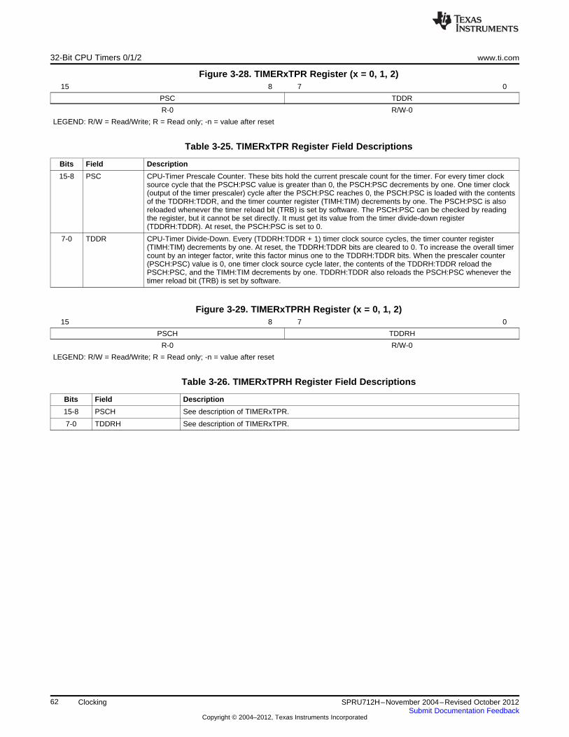
32-Bit CPU Timers 0/1/2 www.ti.com
Figure 3-28. TIMERxTPR Register (x = 0, 1, 2)15 8 7 0
PSC TDDR
R-0 R/W-0
LEGEND: R/W = Read/Write; R = Read only; -n = value after reset
Table 3-25. TIMERxTPR Register Field Descriptions
Bits Field Description
15-8 PSC CPU-Timer Prescale Counter. These bits hold the current prescale count for the timer. For every timer clocksource cycle that the PSCH:PSC value is greater than 0, the PSCH:PSC decrements by one. One timer clock(output of the timer prescaler) cycle after the PSCH:PSC reaches 0, the PSCH:PSC is loaded with the contentsof the TDDRH:TDDR, and the timer counter register (TIMH:TIM) decrements by one. The PSCH:PSC is alsoreloaded whenever the timer reload bit (TRB) is set by software. The PSCH:PSC can be checked by readingthe register, but it cannot be set directly. It must get its value from the timer divide-down register(TDDRH:TDDR). At reset, the PSCH:PSC is set to 0.
7-0 TDDR CPU-Timer Divide-Down. Every (TDDRH:TDDR + 1) timer clock source cycles, the timer counter register(TIMH:TIM) decrements by one. At reset, the TDDRH:TDDR bits are cleared to 0. To increase the overall timercount by an integer factor, write this factor minus one to the TDDRH:TDDR bits. When the prescaler counter(PSCH:PSC) value is 0, one timer clock source cycle later, the contents of the TDDRH:TDDR reload thePSCH:PSC, and the TIMH:TIM decrements by one. TDDRH:TDDR also reloads the PSCH:PSC whenever thetimer reload bit (TRB) is set by software.
Figure 3-29. TIMERxTPRH Register (x = 0, 1, 2)15 8 7 0
PSCH TDDRH
R-0 R/W-0
LEGEND: R/W = Read/Write; R = Read only; -n = value after reset
Table 3-26. TIMERxTPRH Register Field Descriptions
Bits Field Description
15-8 PSCH See description of TIMERxTPR.
7-0 TDDRH See description of TIMERxTPR.
62 Clocking SPRU712H–November 2004–Revised October 2012Submit Documentation Feedback
Copyright © 2004–2012, Texas Instruments Incorporated

Chapter 4SPRU712H–November 2004–Revised October 2012
General-Purpose Input/Output (GPIO)
The GPIO MUX registers are used to select the operation of shared pins on the 280x devices. The pinsare named by their general purpose I/O name i.e. GPIO0 - GPIO34. These pins can be individuallyselected to operate as digital I/O, referred to as GPIO, or connected to one of up to one of threeperipheral I/O signals (via the GPAMUX1, GPAMUX2 and GPBMUX1 registers). If selected for digital I/Omode, registers are provided to configure the pin direction (via the GPADIR and GPBDIR registers). Youcan also qualify the input signals to remove unwanted noise (via the GPAQSEL1, GPAQSEL2,GPBQSEL1 and GPACTRL and GPBCTRL registers).
Topic ........................................................................................................................... Page
4.1 GPIO Module Overview ...................................................................................... 644.2 Configuration Overview ..................................................................................... 654.3 Digital General Purpose I/O Control ..................................................................... 664.4 Input Qualification ............................................................................................. 684.5 GPIO and Peripheral MUXing .............................................................................. 724.6 Register Bit Definitions ...................................................................................... 83
63SPRU712H–November 2004–Revised October 2012 General-Purpose Input/Output (GPIO)Submit Documentation Feedback
Copyright © 2004–2012, Texas Instruments Incorporated

GPxDAT (read)
InputQualification
GPxMUX1/2
High Impedance
Output Control
GPIOx pin
XRS
0 = Input, 1 = Output
Low PowerModes Block
GPxDIR (latch)
Peripheral 2 Input
Peripheral 3 Input
Peripheral 1 Output
Peripheral 2 Output
Peripheral 3 Output
Peripheral 1 Output Enable
Peripheral 2 Output Enable
Peripheral 3 Output Enable
00
01
10
11
00
01
10
11
00
01
10
11
GPxCTRL
Peripheral 1 Input
N/CGPxPUD
LPMCR0
InternalPullup
GPIOLMPSEL
GPxQSEL1/2
GPxSET
GPxDAT (latch)
GPxCLEAR
GPxTOGGLE
GPIOXINT1SEL
GPIOXINT2SEL
GPIOXNMISEL
= Default at Reset
PIEExternal InterruptMUX
GPIO Module Overview www.ti.com
4.1 GPIO Module Overview
On the 280x devices up to three independent peripheral signals are multiplexed on a single GPIO-enabledpin in addition to individual pin bit IO capability. There are two 32-bit IO ports on the 280x devices. Port Aconsists of GPIO0-GPIO31 and port B consists of GPIO32-GPIO34. The remaining IOs on port B arecurrently reserved for future expansion. Figure 4-1 shows the basic modes of operation for the GPIOmodule.
Figure 4-1. Modes of Operation
A x stands for the port, either A or B. For example, GPxDIR refers to either the GPADIR and GPBDIR registerdepending on the particular GPIO pin selected.
B GPxDAT latch/read are accessed at the same memory location.
64 General-Purpose Input/Output (GPIO) SPRU712H–November 2004–Revised October 2012Submit Documentation Feedback
Copyright © 2004–2012, Texas Instruments Incorporated

www.ti.com Configuration Overview
4.2 Configuration Overview
The pin function assignments, input qualification, and the external interrupt (XINT1, XINT2, XNMI) sourcesare all controlled by the GPIO configuration control registers. In addition, you can assign pins to wake thedevice from the HALT and STANDBY low power modes and enable/disable internal pullup resistors.Table 4-1 and Table 4-2 list the registers that are used to configure the GPIO pins to match the systemrequirements.
Table 4-1. GPIO Control Registers
Name (1) Address Size (x16) Register Description Bit Description
GPACTRL 0x6F80 2 GPIO A Control Register (GPIO0-GPIO31) Figure 4-8
GPAQSEL1 0x6F82 2 GPIO A Qualifier Select 1 Register (GPIO0-GPIO15) Figure 4-10
GPAQSEL2 0x6F84 2 GPIO A Qualifier Select 2 Register (GPIO16-GPIO31) Figure 4-11
GPAMUX1 0x6F86 2 GPIO A MUX 1 Register (GPIO0-GPIO15) Figure 4-4
GPAMUX2 0x6F88 2 GPIO A MUX 2 Register (GPIO16-GPIO31) Figure 4-5
GPADIR 0x6F8A 2 GPIO A Direction Register (GPIO0-GPIO31) Figure 4-13
GPAPUD 0x6F8C 2 GPIO A Pull Up Disable Register (GPIO0-GPIO31) Figure 4-15
GPAMCFG 0x6F8E 2 GPIOA Miscellaneous Configuration Register (GPAMCFG) (2) Figure 4-23
GPBCTRL 0x6F90 2 GPIO B Control Register (GPIO32-GPIO34) Figure 4-9
GPBQSEL1 0x6F92 2 GPIO B Qualifier Select 1 Register (GPIO32-GPIO34) Figure 4-12
GPBQSEL2 0x6F94 2 Reserved
GPBMUX1 0x6F96 2 GPIO B MUX 1 Register (GPIO32-GPIO34) Figure 4-6
GPBMUX2 0x6F98 2 Reserved
GPBDIR 0x6F9A 2 GPIO B Direction Register (GPIO32-GPIO34) Figure 4-14
GPBPUD 0x6F9C 2 GPIO B Pull Up Disable Register (GPIO32-GPIO34) Figure 4-16
Reserved 0x6F9E -0x6FB0 34(1) The registers in this table are EALLOW protected. See Section 5.2(2) Applicable on 28044 only
Table 4-2. GPIO Interrupt and Low Power Mode Select Registers
SizeName (1) Address Register Description Bit Description(x16)
GPIOXINT1SEL 0x6FE0 1 XINT1 Source Select Register (GPIO0-GPIO31) Figure 4-21
GPIOXINT2SEL 0x6FE1 1 XINT2 Source Select Register (GPIO0-GPIO31) Figure 4-21
GPIOXNMISEL 0x6FE2 1 XNMI Source Select Register (GPIO0-GPIO31) Figure 4-21
0x6FE3 -Reserved 50x6FE7
GPIOLPMSEL 0x6FE8 1 LPM wakeup Source Select Register (GPIO0-GPIO31) Figure 4-22(1) The registers in this table are EALLOW protected. See Section 5.2 for more information.
65SPRU712H–November 2004–Revised October 2012 General-Purpose Input/Output (GPIO)Submit Documentation Feedback
Copyright © 2004–2012, Texas Instruments Incorporated

Digital General Purpose I/O Control www.ti.com
To plan how to configure the GPIO module, consider the following steps:
1. Plan the device pin-out:Through a pin MUXing scheme, the 280x devices provide flexibility for assigning functionality to the 35GPIO-capable (GPIO0-GPIO34) pins. Before getting started, look at the peripheral options available foreach pin, and plan pin-out for your specific system. Will the pin be used as a general purpose input oroutput (GPIO) or as one of up to three available peripheral functions? Knowing this information willhelp determine how to further configure the pin.
2. Enable or disable internal pullup resistors:To enable or disable the internal pullup resistors, write to the respective bits in the GPIO pullup disable(GPAPUD, GPBPUD) registers. For pins that can function as ePWM output pins (GPIO0-GPIO11), theinternal pullup resistors are disabled by default. All other GPIO-capable pins have the pullup enabledby default.
3. Select input qualification:If the pin will be used as an input, specify the required input qualification, if any. The input qualificationis specified in the GPACTRL, GPBCTRL, GPAQSEL1, GPAQSEL2, and GPBQSEL1 registers. Bydefault, all of the input signals are synchronized to SYSCLKOUT only.
4. Select the pin function:Configure the GPAMUX1, GPAMUX2 and GPBMUX1 registers such that the pin is a GPIO or one ofthree available peripheral functions. By default, all GPIO-capable pins are configured at reset asgeneral purpose input pins.
5. For digital general purpose I/O, select the direction of the pin:If the pin is configured as an GPIO, specify the direction of the pin as either input or output in theGPADIR and GPBDIR registers. By default, all GPIO pins are inputs. To change the pin from input tooutput, first load the output latch with the value to be driven by writing the appropriate value to theGPACLEAR, GPBCLEAR, GPASET, GPBSET, GPATOGGLE or GPBTOGGLE registers. Once theoutput latch is loaded, change the pin direction from input to output via the GPADIR and GPBDIRregisters. The output latch for all pins is cleared at reset.
6. Select low power mode wake-up sources:Specify which pins, if any, will be able to wake the device from HALT and STANDBY low powermodes. The pins are specified in the GPIOLPMSEL register.
7. Select external interrupt sources:Specify the source for the XINT1, XINT2, and XNMI interrupts. For each interrupt you can specify oneof the port A signals as the source. This is done by specifying the source in the GPIOXINT1SEL,GPIOXINT2SEL, and GPIOXNMISEL registers. The polarity of the interrupts can be configured in theXINT1CR, XINT2CR and the XNMICR registers as described in Section 6.6.
4.3 Digital General Purpose I/O Control
For pins that are configured as GPIO you can change the values on the pins by using the followingregisters:
Table 4-3. GPIO Data Registers
Name Address Size (x16) Register Description Bit Description
GPADAT 0x6FC0 2 GPIO A Data Register (GPIO0-GPIO31) Figure 4-17
GPASET 0x6FC2 2 GPIO A Set Register (GPIO0-GPIO31) Figure 4-19
GPACLEAR 0x6FC4 2 GPIO A Clear Register (GPIO0-GPIO31) Figure 4-19
GPATOGGLE 0x6FC6 2 GPIO A Toggle Register (GPIO0-GPIO31) Figure 4-19
GPBDAT 0x6FC8 2 GPIO B Data Register (GPIO32-GPIO34) Figure 4-18
GPBSET 0x6FCA 2 GPIO B Set Register (GPIO32-GPIO34) Figure 4-20
GPBCLEAR 0x6FCC 2 GPIO B Clear Register (GPIO32-GPIO34) Figure 4-20
GPBTOGGLE 0x6FCE 2 GPIO B Toggle Register (GPIO32-GPIO34) Figure 4-20
0x70FC -Reserved 40x70FF
66 General-Purpose Input/Output (GPIO) SPRU712H–November 2004–Revised October 2012Submit Documentation Feedback
Copyright © 2004–2012, Texas Instruments Incorporated

www.ti.com Digital General Purpose I/O Control
• GPADAT, GPBDAT RegistersEach I/O port has one data register. Each bit in the data register corresponds to one GPIO pin. Nomatter how the pin is configured (GPIO or peripheral function), the corresponding bit in the dataregister reflects the current state of the pin after qualification. Writing to the GPADAT or GPBDATregister clears or sets the corresponding output latch and if the pin is enabled as a general purposeoutput (GPIO output) the pin will also be driven either low or high. If the pin is not configured as aGPIO output then the value will be latched, but the pin will not be driven. Only if the pin is laterconfigured as a GPIO output, will the latched value be driven onto the pin.
When using the GPxDAT register to change the level of an output pin, you should be cautious not toaccidentally change the level of another pin. For example, if you mean to change the output latch levelof GPIOA0 by writing to the GPADAT register bit 0, using a read-modify-write instruction. The problemcan occur if another I/O port A signal changes level between the read and the write stage of theinstruction. You can also change the state of that output latch. You can avoid this scenario by usingthe GPxSET, GPxCLEAR, and GPxTOGGLE registers to load the output latch instead.
• GPASET, GPBSET RegistersThe set registers are used to drive specified GPIO pins high without disturbing other pins. Each I/Oport has one set register and each bit corresponds to one GPIO pin. The set registers always readback 0. If the corresponding pin is configured as an output, then writing a 1 to that bit in the set registerwill set the output latch high and the corresponding pin will be driven high. If the pin is not configuredas a GPIO output, then the value will be latched but the pin will not be driven. Only if the pin is laterconfigured as a GPIO output will the latched value will be driven onto the pin. Writing a 0 to any bit inthe set registers has no effect.
• GPACLEAR, GPBCLEAR RegistersThe clear registers are used to drive specified GPIO pins low without disturbing other pins. Each I/Oport has one clear register. The clear registers always read back 0. If the corresponding pin isconfigured as a general purpose output, then writing a 1 to the corresponding bit in the clear registerwill clear the output latch and the pin will be driven low. If the pin is not configured as a GPIO output,then the value will be latched but the pin will not be driven. Only if the pin is later configured as a GPIOoutput will the latched value will be driven onto the pin. Writing a 0 to any bit in the clear registers hasno effect.
• GPATOGGLE, GPBTOGGLE RegistersThe toggle registers are used to drive specified GPIO pins to the opposite level without disturbing otherpins. Each I/O port has one toggle register. The toggle registers always read back 0. If thecorresponding pin is configured as an output, then writing a 1 to that bit in the toggle register flips theoutput latch and pulls the corresponding pin in the opposite direction. That is, if the output pin is drivenlow, then writing a 1 to the corresponding bit in the toggle register will pull the pin high. Likewise, if theoutput pin is high, then writing a 1 to the corresponding bit in the toggle register will pull the pin low. Ifthe pin is not configured as a GPIO output, then the value will be latched but the pin will not be driven.Only if the pin is later configured as a GPIO output will the latched value will be driven onto the pin.Writing a 0 to any bit in the toggle registers has no effect.
67SPRU712H–November 2004–Revised October 2012 General-Purpose Input/Output (GPIO)Submit Documentation Feedback
Copyright © 2004–2012, Texas Instruments Incorporated

GPxCTRL Reg
SYNC
SYSCLKOUT
Qualification Input Signal Qualified By 3 or 6 Samples
GPIOx
Time between samples
GPxQSEL1/2
Number of Samples
Input Qualification www.ti.com
4.4 Input Qualification
Input qualification is very flexible on the 280x devices. You can select the type of input qualification foreach GPIO pin by configuring the GPAQSEL1, GPAQSEL2 and GPBQSEL1 registers. In the case of aGPIO input pin, the qualification can be specified as only synchronize to SYSCLKOUT or qualification by asampling window. For pins that are configured as peripheral inputs, the input can also be asynchronous inaddition to synchronized to SYSCLKOUT or qualified by a sampling window. The remainder of this sectiondescribes the options available.
4.4.1 No synchronization (asynchronous input):
This mode is used for peripherals where input synchronization is not required or the peripheral itselfperforms the synchronization. Examples include communication ports SCI, SPI, eCAN, and I2C. Inaddition, it may be desirable to have the ePWM trip zone (TZ1-TZ6) signals function independent of thepresence of SYSCLKOUT.
The asynchronous option is not valid if the pin is used as a general purpose digital input pin (GPIO). If thepin is configured as a GPIO input and the asynchronous option is selected then the qualification defaultsto synchronization to SYSCLKOUT as described in Section 4.4.2.
4.4.2 Synchronization to SYSCLKOUT only:
This is the default qualification mode of all the pins at reset. In this mode, the input signal is onlysynchronized to the system clock (SYSCLKOUT). Because the incoming signal is asynchronous, it cantake up to a SYSCLKOUT period of delay in order for the input to the DSP to be changed. No furtherqualification is performed on the signal.
4.4.3 Qualification using a sampling window:
In this mode, the signal is first synchronized to the system clock (SYSCLKOUT) and then qualified by aspecified number of cycles before the input is allowed to change. Figure 4-2 and Figure 4-3 show how theinput qualification is performed to eliminate unwanted noise. Two parameters are specified by the user forthis type of qualification: 1) the sampling period, or how often the signal is sampled, and 2) the number ofsamples to be taken.
Figure 4-2. Input Qualification Using a Sampling Window
68 General-Purpose Input/Output (GPIO) SPRU712H–November 2004–Revised October 2012Submit Documentation Feedback
Copyright © 2004–2012, Texas Instruments Incorporated

www.ti.com Input Qualification
Time between samples (sampling period):
To qualify the signal, the input signal is sampled at a regular period. The sampling period is specified bythe user and determines the time duration between samples, or how often the signal will be sampled,relative to the CPU clock (SYSCLKOUT).
The sampling period is specified by the qualification period (QUALPRDn) bits in the GPACTRL orGPBCTRL register. The sampling period is configurable in groups of 8 input signals. For example, GPIO0to GPIO7 use GPACTRL[QUALPRD0] setting and GPIO8 to GPIO15 use GPACTRL[QUALPRD1].Table 4-4 and Table 4-5 show the relationship between the sampling period or sampling frequency andthe GPxCTRL[QUALPRDn] setting.
Table 4-4. Sampling Period
Sampling Period
If GPxCTRL[QUALPRDn] = 0 1 × TSYSCLKOUT
If GPxCTRL[QUALPRDn] ≠ 0 2 × GPxCTRL[QUALPRDn] × TSYSCLKOUT
Where TSYSCLKOUT is the period in time of SYSCLKOUT
Table 4-5. Sampling Frequency
Sampling Frequency
If GPxCTRL[QUALPRDn] = 0 fSYSCLKOUT
If GPxCTRL[QUALPRDn] ≠ 0 fSYSCLKOUT × 1 ÷ (2 × GPxCTRL[QUALPRDn])
Where fSYSCLKOUT is the frequency of SYSCLKOUT
From these equations, the minimum and maximum time between samples can be calculated for a givenSYSCLKOUT frequency:
Example: Maximum Sampling Frequency:
If GPxCTRL[QUALPRDn] = 0
then the sampling frequency is fSYSCLKOUT
If, for example, fSYSCLKOUT = 100MHz
then the signal will be sampled at 100MHz or one sample every 10ns.
Example: Minimum Sampling Frequency:
If GPxCTRL[QUALPRDn] = 0xFF (i.e. 255)
then the sampling frequency is fSYSCLKOUT × 1 ÷ (2 × GPxCTRL[QUALPRDn])
If, for example, fSYSCLKOUT = 100MHz
then the signal will be sampled at 100MHz × 1 ÷ (2 × 255) or one sample every 5.1uS.
69SPRU712H–November 2004–Revised October 2012 General-Purpose Input/Output (GPIO)Submit Documentation Feedback
Copyright © 2004–2012, Texas Instruments Incorporated

Input Qualification www.ti.com
Number of samples:
The number of times the signal is sampled is either 3 samples or 6 samples as specified in thequalification selection (GPAQSEL1, GPAQSEL2 and GPBQSEL1) registers. When 3 or 6 consecutivecycles are the same, then the input change will be passed through to the DSP.
Total Sampling Window Width:
The sampling window is the time during which the input signal will be sampled as shown in Figure 4-3. Byusing the equation for the sampling period along with the number of samples to be taken, the total width ofthe window can be determined.
For the input qualifier to detect a change in the input, the level of the signal must be stable for the durationof the sampling window width or longer.
The number of sampling periods within the window is always one less then the number of samples taken.For a thee-sample window, the sampling window width is 2 sampling periods wide where the samplingperiod is defined in Table 4-4. Likewise, for a six-sample window, the sampling window width is 5sampling periods wide. Table 4-6 and Table 4-7 show the calculations that can be used to determine thetotal sampling window width based on GPxCTRL[QUALPRDn] and the number of samples taken.
Table 4-6. Case 1: Three-Sample Sampling Window Width
Total Sampling Window Width
If GPxCTRL[QUALPRDn] = 0 2 × TSYSCLKOUT
If GPxCTRL[QUALPRDn] ≠ 0 2 × 2 × GPxCTRL[QUALPRDn] × TSYSCLKOUT
Where TSYSCLKOUT is the period in time of SYSCLKOUT
Table 4-7. Case 2: Six-Sample Sampling Window Width
Total Sampling Window Width
If GPxCTRL[QUALPRDn] = 0 5 × TSYSCLKOUT
If GPxCTRL[QUALPRDn] ≠ 0 5 × 2 × GPxCTRL[QUALPRDn] × TSYSCLKOUT
Where TSYSCLKOUT is the period in time of SYSCLKOUT
NOTE: The external signal change is asynchronous with respect to both the sampling period andSYSCLKOUT. Due to the asynchronous nature of the external signal, the input should beheld stable for a time greater than the sampling window width to make sure the logic detectsa change in the signal. The extra time required can be up to an additional sampling period +TSYSCLKOUT.
The required duration for an input signal to be stable for the qualification logic to detect achange is described in the device specific data manual.
70 General-Purpose Input/Output (GPIO) SPRU712H–November 2004–Revised October 2012Submit Documentation Feedback
Copyright © 2004–2012, Texas Instruments Incorporated
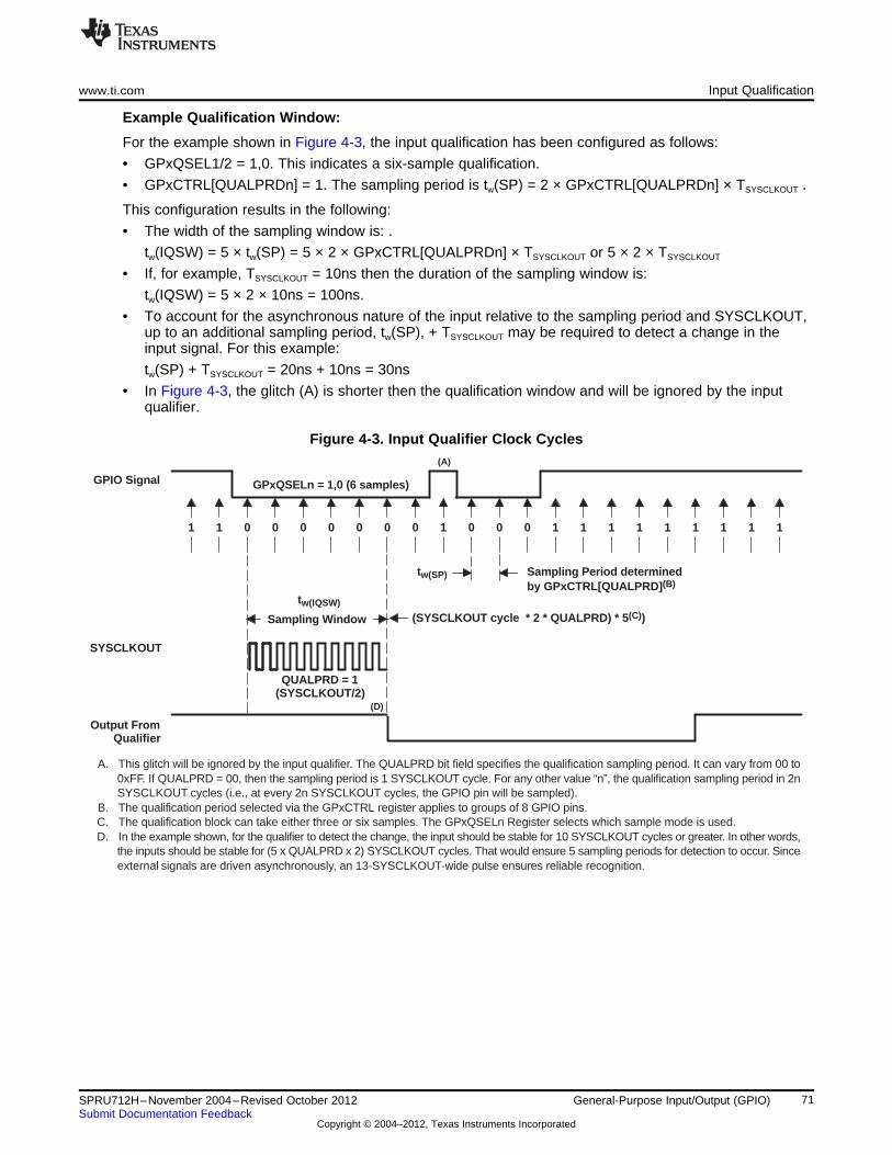
GPIO Signal
1
Sampling Window
Output FromQualifier
1 1 1 1 1 1 1 1 1 1 10 0 0 0 0 0 0 0 0 0
SYSCLKOUT
QUALPRD = 1(SYSCLKOUT/2)
(SYSCLKOUT cycle * 2 * QUALPRD) * 5(C))
(A)
GPxQSELn = 1,0 (6 samples)
Sampling Period determined by GPxCTRL[QUALPRD](B)
A. This glitch will be ignored by the input qualifier. The QUALPRD bit field specifies the qualification sampling period. It can vary from 00 to0xFF. If QUALPRD = 00, then the sampling period is 1 SYSCLKOUT cycle. For any other value “n”, the qualification sampling period in 2nSYSCLKOUT cycles (i.e., at every 2n SYSCLKOUT cycles, the GPIO pin will be sampled).
B. The qualification period selected via the GPxCTRL register applies to groups of 8 GPIO pins.C. The qualification block can take either three or six samples. The GPxQSELn Register selects which sample mode is used.D. In the example shown, for the qualifier to detect the change, the input should be stable for 10 SYSCLKOUT cycles or greater. In other words,
the inputs should be stable for (5 x QUALPRD x 2) SYSCLKOUT cycles. That would ensure 5 sampling periods for detection to occur. Sinceexternal signals are driven asynchronously, an 13-SYSCLKOUT-wide pulse ensures reliable recognition.
(D)
tw(SP)
tw(IQSW)
www.ti.com Input Qualification
Example Qualification Window:
For the example shown in Figure 4-3, the input qualification has been configured as follows:
• GPxQSEL1/2 = 1,0. This indicates a six-sample qualification.
• GPxCTRL[QUALPRDn] = 1. The sampling period is tw(SP) = 2 × GPxCTRL[QUALPRDn] × TSYSCLKOUT .
This configuration results in the following:
• The width of the sampling window is: .
tw(IQSW) = 5 × tw(SP) = 5 × 2 × GPxCTRL[QUALPRDn] × TSYSCLKOUT or 5 × 2 × TSYSCLKOUT
• If, for example, TSYSCLKOUT = 10ns then the duration of the sampling window is:
tw(IQSW) = 5 × 2 × 10ns = 100ns.
• To account for the asynchronous nature of the input relative to the sampling period and SYSCLKOUT,up to an additional sampling period, tw(SP), + TSYSCLKOUT may be required to detect a change in theinput signal. For this example:
tw(SP) + TSYSCLKOUT = 20ns + 10ns = 30ns
• In Figure 4-3, the glitch (A) is shorter then the qualification window and will be ignored by the inputqualifier.
Figure 4-3. Input Qualifier Clock Cycles
71SPRU712H–November 2004–Revised October 2012 General-Purpose Input/Output (GPIO)Submit Documentation Feedback
Copyright © 2004–2012, Texas Instruments Incorporated

GPIO and Peripheral MUXing www.ti.com
4.5 GPIO and Peripheral MUXing
The 280x devices MUX up to three different peripheral functions along with a general input/output (GPIO)port per pin. This allows you to pick and choose a peripheral mix that will work best for the particularapplication.
Table 4-9, Table 4-10, and Table 4-10 show an overview of the possible MUX combinations sorted byGPIO pin. The second column indicates the I/O name of the pin on the device. Since the I/O name isunique, it is the best way to identify a particular pin. Therefore, the register descriptions in this section onlyrefer to the GPIO name of a particular pin. The MUX register and particular bits that control the selectionfor each pin are indicated in the first column.
For example, the MUX for the GPIO7 pin is controlled by writing to GPAMUX[15:14]. By writing to thesebits, the pin is configured as either GPIO7, or one of up to three peripheral functions. The GPIO7 pin on a2808 can be configured as follows:
GPAMUX1[15:14] Bit Setting Pin Functionality Selected
If GPAMUX1[15:14] = 0,0 Pin configured as GPIO7
If GPAMUX1[15:14] = 0,1 Pin configured as EPWM4B (O)
If GPAMUX1[15:14] = 1,0 Pin configured as SPISTED (I/O)
If GPAMUX1[15:14] = 1,1 Pin configured as ECAP2 (I/O)
All the devices in the 280x family have the same MUXing scheme. The only difference is that if aperipheral is not available on a particular device, that MUX selection is reserved on that device and shouldnot be used.
NOTE: If you should select a reserved GPIO MUX configuration that is not mapped to a peripheral,the state of the pin will be undefined and the pin may be driven. Reserved configurations arefor future expansion and should not be selected. In the device MUX tables (Table 4-9,Table 4-10, and Table 4-11) these options are indicated as "Reserved".
Some peripherals can be assigned to more than one pin via the MUX registers. For example, the CAP1function can be assigned to either the GPIO5 or GPIO24 pin, depending on individual systemrequirements as shown below:
Pin Assigned to CAP1 MUX Configuration
Choice 1 GPIO5 GPAMUX1[11:10] = 1,1
or Choice 2 GPIO24 GPAMUX2[17:16] = 0,1
If no pin is configured as an input to a peripheral, or if more then one pin is configured as an input for thesame peripheral, then the input to the peripheral will either default to a 0 or a 1 as shown in Table 4-8. Forexample, if ECAP1 were assigned to both GPIO5 and GPIO24, the input to the eCAP1 peripheral woulddefault to a high state as shown in Table 4-8 and the input would not be connected to GPIO5 or GPIO24.
The 28044 device has an additional level of muxing for the PWM pins. The specific PWM signal that isoutput on the PWM pins is dependent on the GPAMCFG[EPWMMODE] bits.
72 General-Purpose Input/Output (GPIO) SPRU712H–November 2004–Revised October 2012Submit Documentation Feedback
Copyright © 2004–2012, Texas Instruments Incorporated
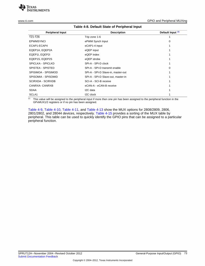
www.ti.com GPIO and Peripheral MUXing
Table 4-8. Default State of Peripheral Input
Peripheral Input Description Default Input (1)
TZ1-TZ6 Trip zone 1-6 1
EPWMSYNCI ePWM Synch Input 0
ECAP1-ECAP4 eCAP1-4 input 1
EQEP1A, EQEP2A eQEP input 1
EQEP1I, EQEP2I eQEP index 1
EQEP1S, EQEP2S eQEP strobe 1
SPICLKA - SPICLKD SPI-A - SPI-D clock 1
SPISTEA - SPISTED SPI-A - SPI-D transmit enable 0
SPISIMOA - SPISIMOD SPI-A - SPI-D Slave-in, master-out 1
SPISOMIA - SPISOMID SPI-A - SPI-D Slave-out, master-in 1
SCIRXDA - SCIRXDB SCI-A - SCI-B receive 1
CANRXA- CANRXB eCAN-A - eCAN-B receive 1
SDAA I2C data 1
SCLA1 I2C clock 1(1) This value will be assigned to the peripheral input if more then one pin has been assigned to the peripheral function in the
GPxMUX1/2 registers or if no pin has been assigned.
Table 4-9, Table 4-10, Table 4-11, and Table 4-13 show the MUX options for 2808/2809, 2806,2801/2802, and 28044 devices, respectively. Table 4-15 provides a sorting of the MUX table byperipheral. This table can be used to quickly identify the GPIO pins that can be assigned to a particularperipheral function.
73SPRU712H–November 2004–Revised October 2012 General-Purpose Input/Output (GPIO)Submit Documentation Feedback
Copyright © 2004–2012, Texas Instruments Incorporated

GPIO and Peripheral MUXing www.ti.com
Table 4-9. 2809 and 2808 GPIO MUX
Default at ResetGPAMUX1/2 (1) Primary I/O Function Peripheral Selection 1 Peripheral Selection 2 Peripheral Selection 3Register Bits (GPxMUX1/2 bits=0,0) (GPxMUX1/2 bits=0,1) (2) (GPxMUX1/2 bits=1,0) (2) (GPxMUX1/2 bits=1,1) (2)
GPAMUX1
1-0 GPIO0 EPWM1A (O) Reserved Reserved
3-2 GPIO1 EPWM1B (O) SPISIMOD (I/O) Reserved
5-4 GPIO2 EPWM2A (O) Reserved Reserved
7-6 GPIO3 EPWM2B (O) SPISOMID (I/O) Reserved
9-8 GPIO4 EPWM3A (O) Reserved Reserved
11-10 GPIO5 EPWM3B (O) SPICLKD (I/O) ECAP1 (I/O)
13-12 GPIO6 EPWM4A (O) EPWMSYNCI (I) EPWMSYNCO (O)
15-14 GPIO7 EPWM4B (O) SPISTED (I/O) ECAP2 (I/O)
17-16 GPIO8 EPWM5A (O) CANTXB (O) ADCSOCAO (O)
19-18 GPIO9 EPWM5B (O) SCITXDB (O) ECAP3 (I/O)
21-20 GPIO10 EPWM6A (O) CANRXB (I) ADCSOCBO (O)
23-22 GPIO11 EPWM6B (O) SCIRXDB (I) ECAP4 (I/O)
25-24 GPIO12 TZ1 (I) CANTXB (O) SPISIMOB (I/O)
27-26 GPIO13 TZ2 (I) CANRXB (I) SPISOMIB (I/O)
29-28 GPIO14 TZ3 (I) SCITXDB (O) SPICLKB (I/O)
31-30 GPIO15 TZ4 (I) SCIRXDB (I) SPISTEB (I/O)
GPAMUX2
1-0 GPIO16 SPISIMOA (I/O) CANTXB (O) TZ5 (I)
3-2 GPIO17 SPISOMIA (I/O) CANRXB (I) TZ6 (I)
5-4 GPIO18 SPICLKA (I/O) SCITXDB (O) Reserved
7-6 GPIO19 SPISTEA (I/O) SCIRXDB (I) Reserved
9-8 GPIO20 EQEP1A (I) SPISIMOC (I/O) CANTXB (O)
11-10 GPIO21 EQEP1B (I) SPISOMIC (I/O) CANRXB (I)
13-12 GPIO22 EQEP1S (I/O) SPICLKC (I/O) SCITXDB (O)
15-14 GPIO23 EQEP1I (I/O) SPISTEC (I/O) SCIRXDB (I)
17-16 GPIO24 ECAP1 (I/O) EQEP2A (I) SPISIMOB (I/O)
19-18 GPIO25 ECAP2 (I/O) EQEP2B (I) SPISOMIB (I/O)
21-20 GPIO26 ECAP3 (I/O) EQEP2I (I/O) SPICLKB (I/O)
23-22 GPIO27 ECAP4 (I/O) EQEP2S (I/O) SPISTEB (I/O)
25-24 GPIO28 SCIRXDA (I) Reserved TZ5 (I)
27-26 GPIO29 SCITXDA (O) Reserved TZ6 (I)
29-28 GPIO30 CANRXA (I) Reserved Reserved
31-30 GPIO31 CANTXA (O) Reserved Reserved
GPBMUX1
1-0 GPIO32 SDAA (I/OC) EPWMSYNCI (I) ADCSOCAO (O)
3-2 GPIO33 SCLA (I/OC) EPWMSYNCO (O) ADCSOCBO (O)
5-4 GPIO34 Reserved Reserved Reserved(1) GPxMUX1/2 refers to the appropriate MUX register for the pin; GPAMUX1, GPAMUX2 or GPBMUX1.(2) "Reserved" means that there is no peripheral assigned to this GPxMUX1/2 register setting. Should it be selected, the state of the
pin will be undefined and the pin may be driven. This selection is a reserved configuration for future expansion.
74 General-Purpose Input/Output (GPIO) SPRU712H–November 2004–Revised October 2012Submit Documentation Feedback
Copyright © 2004–2012, Texas Instruments Incorporated

www.ti.com GPIO and Peripheral MUXing
Table 4-10. 2806 GPIO MUX
Default at ResetGPxMUX1/2 (1) Primary I/O Function Peripheral Selection 1 Peripheral Selection 2 Peripheral Selection 3Register Bits (GPxMUX1/2 bits=0,0) (GPxMUX1/2 bits=0,1) (2) (GPxMUX1/2 bits=1,0) (2) (GPxMUX1/2 bits=1,1) (2)
GPAMUX1
1-0 GPIO0 EPWM1A (O) Reserved Reserved
3-2 GPIO1 EPWM1B (O) SPISIMOD (I/O) Reserved
5-4 GPIO2 EPWM2A (O) Reserved Reserved
7-6 GPIO3 EPWM2B (O) SPISOMID (I/O) Reserved
9-8 GPIO4 EPWM3A (O) Reserved Reserved
11-10 GPIO5 EPWM3B (O) SPICLKD (I/O) ECAP1 (I/O)
13-12 GPIO6 EPWM4A (O) EPWMSYNCI (I) EPWMSYNCO (O)
15-14 GPIO7 EPWM4B (O) SPISTED (I/O) ECAP2 (I/O)
17-16 GPIO8 EPWM5A (O) Reserved ADCSOCAO (O)
19-18 GPIO9 EPWM5B (O) SCITXDB (O) ECAP3 (I/O)
21-20 GPIO10 EPWM6A (O) Reserved ADCSOCBO (O)
23-22 GPIO11 EPWM6B (O) SCIRXDB (I) ECAP4 (I/O)
25-24 GPIO12 TZ1 (I) Reserved SPISIMOB (I/O)
27-26 GPIO13 TZ2 (I) Reserved SPISOMIB (I/O)
29-28 GPIO14 TZ3 (I) SCITXDB (O) SPICLKB (I/O)
31-30 GPIO15 TZ4 (I) SCIRXDB (I) SPISTEB (I/O)
GPAMUX2
1-0 GPIO16 SPISIMOA (I/O) Reserved TZ5 (I)
3-2 GPIO17 SPISOMIA (I/O) Reserved TZ6 (I)
5-4 GPIO18 SPICLKA (I/O) SCITXDB (O) Reserved
7-6 GPIO19 SPISTEA (I/O) SCIRXDB (I) Reserved
9-8 GPIO20 EQEP1A (I) SPISIMOC (I/O) Reserved
11-10 GPIO21 EQEP1B (I) SPISOMIC (I/O) Reserved
13-12 GPIO22 EQEP1S (I/O) SPICLKC (I/O) SCITXDB (O)
15-14 GPIO23 EQEP1I (I/O) SPISTEC (I/O) SCIRXDB (I)
17-16 GPIO24 ECAP1 (I/O) EQEP2A (I) SPISIMOB (I/O)
19-18 GPIO25 ECAP2 (I/O) EQEP2B (I) SPISOMIB (I/O)
21-20 GPIO26 ECAP3 (I/O) EQEP2I (I/O) SPICLKB (I/O)
23-22 GPIO27 ECAP4 (I/O) EQEP2S (I/O) SPISTEB (I/O)
25-24 GPIO28 SCIRXDA (I) Reserved TZ5 (I)
27-26 GPIO29 SCITXDA (O) Reserved TZ6 (I)
29-28 GPIO30 CANRXA (I) Reserved Reserved
31-30 GPIO31 CANTXA (O) Reserved Reserved
GPBMUX1
1-0 GPIO32 SDAA (I/OC) EPWMSYNCI (I) ADCSOCAO (O)
3-2 GPIO33 SCLA (I/OC) EPWMSYNCO (O) ADCSOCBO (O)
5-4 GPIO34 Reserved Reserved Reserved(1) GPxMUX1/2 refers to the appropriate MUX register for the pin; GPAMUX1, GPAMUX2 or GPBMUX1.(2) "Reserved" means that there is no peripheral assigned to this GPxMUX1/2 register setting. Should it be selected, the state of the
pin will be undefined and the pin may be driven. This selection is a reserved configuration for future expansion.
75SPRU712H–November 2004–Revised October 2012 General-Purpose Input/Output (GPIO)Submit Documentation Feedback
Copyright © 2004–2012, Texas Instruments Incorporated
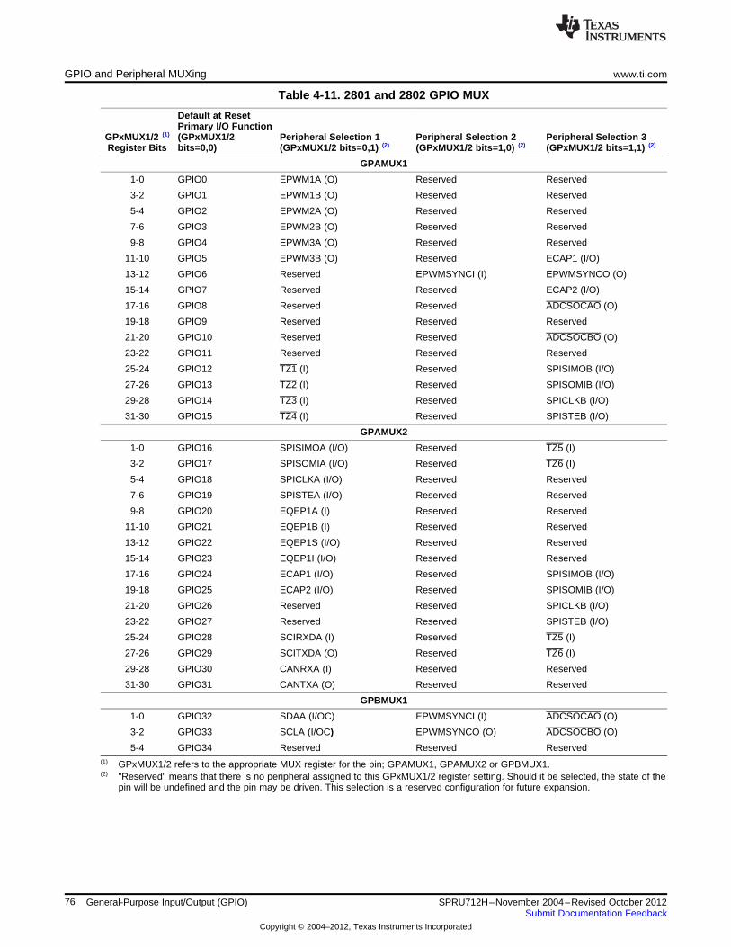
GPIO and Peripheral MUXing www.ti.com
Table 4-11. 2801 and 2802 GPIO MUX
Default at ResetPrimary I/O Function
GPxMUX1/2 (1) (GPxMUX1/2 Peripheral Selection 1 Peripheral Selection 2 Peripheral Selection 3Register Bits bits=0,0) (GPxMUX1/2 bits=0,1) (2) (GPxMUX1/2 bits=1,0) (2) (GPxMUX1/2 bits=1,1) (2)
GPAMUX1
1-0 GPIO0 EPWM1A (O) Reserved Reserved
3-2 GPIO1 EPWM1B (O) Reserved Reserved
5-4 GPIO2 EPWM2A (O) Reserved Reserved
7-6 GPIO3 EPWM2B (O) Reserved Reserved
9-8 GPIO4 EPWM3A (O) Reserved Reserved
11-10 GPIO5 EPWM3B (O) Reserved ECAP1 (I/O)
13-12 GPIO6 Reserved EPWMSYNCI (I) EPWMSYNCO (O)
15-14 GPIO7 Reserved Reserved ECAP2 (I/O)
17-16 GPIO8 Reserved Reserved ADCSOCAO (O)
19-18 GPIO9 Reserved Reserved Reserved
21-20 GPIO10 Reserved Reserved ADCSOCBO (O)
23-22 GPIO11 Reserved Reserved Reserved
25-24 GPIO12 TZ1 (I) Reserved SPISIMOB (I/O)
27-26 GPIO13 TZ2 (I) Reserved SPISOMIB (I/O)
29-28 GPIO14 TZ3 (I) Reserved SPICLKB (I/O)
31-30 GPIO15 TZ4 (I) Reserved SPISTEB (I/O)
GPAMUX2
1-0 GPIO16 SPISIMOA (I/O) Reserved TZ5 (I)
3-2 GPIO17 SPISOMIA (I/O) Reserved TZ6 (I)
5-4 GPIO18 SPICLKA (I/O) Reserved Reserved
7-6 GPIO19 SPISTEA (I/O) Reserved Reserved
9-8 GPIO20 EQEP1A (I) Reserved Reserved
11-10 GPIO21 EQEP1B (I) Reserved Reserved
13-12 GPIO22 EQEP1S (I/O) Reserved Reserved
15-14 GPIO23 EQEP1I (I/O) Reserved Reserved
17-16 GPIO24 ECAP1 (I/O) Reserved SPISIMOB (I/O)
19-18 GPIO25 ECAP2 (I/O) Reserved SPISOMIB (I/O)
21-20 GPIO26 Reserved Reserved SPICLKB (I/O)
23-22 GPIO27 Reserved Reserved SPISTEB (I/O)
25-24 GPIO28 SCIRXDA (I) Reserved TZ5 (I)
27-26 GPIO29 SCITXDA (O) Reserved TZ6 (I)
29-28 GPIO30 CANRXA (I) Reserved Reserved
31-30 GPIO31 CANTXA (O) Reserved Reserved
GPBMUX1
1-0 GPIO32 SDAA (I/OC) EPWMSYNCI (I) ADCSOCAO (O)
3-2 GPIO33 SCLA (I/OC) EPWMSYNCO (O) ADCSOCBO (O)
5-4 GPIO34 Reserved Reserved Reserved(1) GPxMUX1/2 refers to the appropriate MUX register for the pin; GPAMUX1, GPAMUX2 or GPBMUX1.(2) "Reserved" means that there is no peripheral assigned to this GPxMUX1/2 register setting. Should it be selected, the state of the
pin will be undefined and the pin may be driven. This selection is a reserved configuration for future expansion.
76 General-Purpose Input/Output (GPIO) SPRU712H–November 2004–Revised October 2012Submit Documentation Feedback
Copyright © 2004–2012, Texas Instruments Incorporated

www.ti.com GPIO and Peripheral MUXing
Table 4-12. TMS320F28016/TMS320F28015 GPIO MUX
Default at ResetPrimary I/O Function
GPxMUX1/2 (1) (GPxMUX1/2 Peripheral Selection 1 Peripheral Selection 2 Peripheral Selection 3Register Bits bits=0,0) (GPxMUX1/2 bits=0,1) (2) (GPxMUX1/2 bits=1,0) (2) (GPxMUX1/2 bits=1,1) (2)
GPAMUX1
1-0 GPIO0 EPWM1A (O) Reserved Reserved
3-2 GPIO1 EPWM1B (O) Reserved Reserved
5-4 GPIO2 EPWM2A (O) Reserved Reserved
7-6 GPIO3 EPWM2B (O) Reserved Reserved
9-8 GPIO4 EPWM3A (O) Reserved Reserved
11-10 GPIO5 EPWM3B (O) Reserved ECAP1 (I/O)
13-12 GPIO6 EPWM4A (O) EPWMSYNCI (I) EPWMSYNCO (O)
15-14 GPIO7 EPWM4B (O) Reserved ECAP2 (I/O)
17-16 GPIO8 Reserved Reserved ADCSOCAO (O)
19-18 GPIO9 Reserved Reserved Reserved
21-20 GPIO10 Reserved Reserved ADCSOCBO (O)
23-22 GPIO11 Reserved Reserved Reserved
25-24 GPIO12 TZ1 (I) Reserved SPISIMOB (I/O)
27-26 GPIO13 TZ2 (I) Reserved SPISOMIB (I/O)
29-28 GPIO14 TZ3 (I) Reserved SPICLKB (I/O)
31-30 GPIO15 TZ4 (I) Reserved SPISTEB (I/O)
GPAMUX2
1-0 GPIO16 SPISIMOA (I/O) Reserved TZ5 (I)
3-2 GPIO17 SPISOMIA (I/O) Reserved TZ6 (I)
5-4 GPIO18 SPICLKA (I/O) Reserved Reserved
7-6 GPIO19 SPISTEA (I/O) Reserved Reserved
9-8 GPIO20 Reserved Reserved Reserved
11-10 GPIO21 Reserved Reserved Reserved
13-12 GPIO22 Reserved Reserved Reserved
15-14 GPIO23 Reserved Reserved Reserved
17-16 GPIO24 ECAP1 (I/O) Reserved Reserved
19-18 GPIO25 ECAP2 (I/O) Reserved Reserved
21-20 GPIO26 Reserved Reserved Reserved
23-22 GPIO27 Reserved Reserved Reserved
25-24 GPIO28 SCIRXDA (I) Reserved TZ5 (I)
27-26 GPIO29 SCITXDA (O) Reserved TZ6 (I)
29-28 GPIO30 CANRXA (I) (3) Reserved Reserved
31-30 GPIO31 CANTXA (O) (3) Reserved Reserved
GPBMUX1
1-0 GPIO32 SDAA (I/OC) EPWMSYNCI (I) ADCSOCAO (O)
3-2 GPIO33 SCLA (I/OC) EPWMSYNCO (O) ADCSOCBO (O)
5-4 GPIO34 Reserved Reserved Reserved(1) GPxMUX1/2 refers to the appropriate MUX register for the pin; GPAMUX1, GPAMUX2 or GPBMUX1.(2) "Reserved" means that there is no peripheral assigned to this GPxMUX1/2 register setting. Should it be selected, the state of the
pin will be undefined and the pin may be driven. This selection is a reserved configuration for future expansion.(3) This function is not available in the F28015 device.
77SPRU712H–November 2004–Revised October 2012 General-Purpose Input/Output (GPIO)Submit Documentation Feedback
Copyright © 2004–2012, Texas Instruments Incorporated
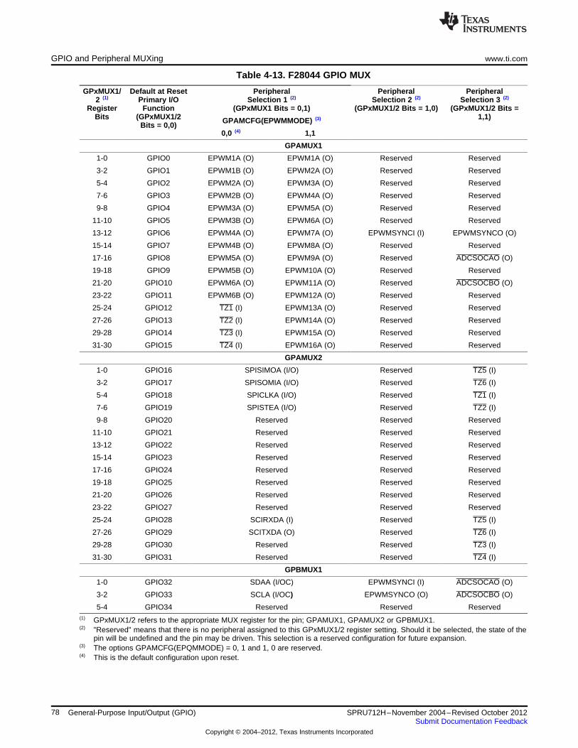
GPIO and Peripheral MUXing www.ti.com
Table 4-13. F28044 GPIO MUX
GPxMUX1/ Default at Reset Peripheral Peripheral Peripheral2 (1) Primary I/O Selection 1 (2) Selection 2 (2) Selection 3 (2)
Register Function (GPxMUX1 Bits = 0,1) (GPxMUX1/2 Bits = 1,0) (GPxMUX1/2 Bits =Bits (GPxMUX1/2 1,1)GPAMCFG(EPWMMODE) (3)
Bits = 0,0)0,0 (4) 1,1
GPAMUX1
1-0 GPIO0 EPWM1A (O) EPWM1A (O) Reserved Reserved
3-2 GPIO1 EPWM1B (O) EPWM2A (O) Reserved Reserved
5-4 GPIO2 EPWM2A (O) EPWM3A (O) Reserved Reserved
7-6 GPIO3 EPWM2B (O) EPWM4A (O) Reserved Reserved
9-8 GPIO4 EPWM3A (O) EPWM5A (O) Reserved Reserved
11-10 GPIO5 EPWM3B (O) EPWM6A (O) Reserved Reserved
13-12 GPIO6 EPWM4A (O) EPWM7A (O) EPWMSYNCI (I) EPWMSYNCO (O)
15-14 GPIO7 EPWM4B (O) EPWM8A (O) Reserved Reserved
17-16 GPIO8 EPWM5A (O) EPWM9A (O) Reserved ADCSOCAO (O)
19-18 GPIO9 EPWM5B (O) EPWM10A (O) Reserved Reserved
21-20 GPIO10 EPWM6A (O) EPWM11A (O) Reserved ADCSOCBO (O)
23-22 GPIO11 EPWM6B (O) EPWM12A (O) Reserved Reserved
25-24 GPIO12 TZ1 (I) EPWM13A (O) Reserved Reserved
27-26 GPIO13 TZ2 (I) EPWM14A (O) Reserved Reserved
29-28 GPIO14 TZ3 (I) EPWM15A (O) Reserved Reserved
31-30 GPIO15 TZ4 (I) EPWM16A (O) Reserved Reserved
GPAMUX2
1-0 GPIO16 SPISIMOA (I/O) Reserved TZ5 (I)
3-2 GPIO17 SPISOMIA (I/O) Reserved TZ6 (I)
5-4 GPIO18 SPICLKA (I/O) Reserved TZ1 (I)
7-6 GPIO19 SPISTEA (I/O) Reserved TZ2 (I)
9-8 GPIO20 Reserved Reserved Reserved
11-10 GPIO21 Reserved Reserved Reserved
13-12 GPIO22 Reserved Reserved Reserved
15-14 GPIO23 Reserved Reserved Reserved
17-16 GPIO24 Reserved Reserved Reserved
19-18 GPIO25 Reserved Reserved Reserved
21-20 GPIO26 Reserved Reserved Reserved
23-22 GPIO27 Reserved Reserved Reserved
25-24 GPIO28 SCIRXDA (I) Reserved TZ5 (I)
27-26 GPIO29 SCITXDA (O) Reserved TZ6 (I)
29-28 GPIO30 Reserved Reserved TZ3 (I)
31-30 GPIO31 Reserved Reserved TZ4 (I)
GPBMUX1
1-0 GPIO32 SDAA (I/OC) EPWMSYNCI (I) ADCSOCAO (O)
3-2 GPIO33 SCLA (I/OC) EPWMSYNCO (O) ADCSOCBO (O)
5-4 GPIO34 Reserved Reserved Reserved(1) GPxMUX1/2 refers to the appropriate MUX register for the pin; GPAMUX1, GPAMUX2 or GPBMUX1.(2) "Reserved" means that there is no peripheral assigned to this GPxMUX1/2 register setting. Should it be selected, the state of the
pin will be undefined and the pin may be driven. This selection is a reserved configuration for future expansion.(3) The options GPAMCFG(EPQMMODE) = 0, 1 and 1, 0 are reserved.(4) This is the default configuration upon reset.
78 General-Purpose Input/Output (GPIO) SPRU712H–November 2004–Revised October 2012Submit Documentation Feedback
Copyright © 2004–2012, Texas Instruments Incorporated
www.ti.com GPIO and Peripheral MUXing
79SPRU712H–November 2004–Revised October 2012 General-Purpose Input/Output (GPIO)Submit Documentation Feedback
Copyright © 2004–2012, Texas Instruments Incorporated

GPIO and Peripheral MUXing www.ti.com
Table 4-14 is a GPxMUX1/2 register table sorted by peripheral function instead of GPIO function. Thistable shows the super set of peripherals that are available on the 2808 device. Some peripherals shownwill not be available on other devices and should be considered reserved. The behavior of reservedlocations on each device are described in Table 4-9, Table 4-10, and Table 4-11. This table can be usedto help identify the GPIO pins that can be assigned to a particular peripheral function. It is suggested thatthe final selection be cross checked with your specific device's data manual.
Table 4-14. Peripheral to GPIO Cross Reference
Primary I/O Function Peripheral Selection 1 Peripheral Selection 2 Peripheral Selection 3(GPxMUX1/2 bits=0,0) (GPxMUX1/2 bits=0,1) (GPxMUX1/2 bits=1,0) (GPxMUX1/2 bits=1,1)
ADC External Start of Conversion A
GPIO8 EPWM5A CANTXB ADCSOCAO
GPIO32 SDAA EPWMSYNCI ADCSOCAO
ADC External Start of Conversion B
GPIO10 EPWM6A CANRXB ADCSOCBO
GPIO10 EPWM6A CANRXB ADCSOCBO
GPIO33 SCLA EPWMSYNCO ADCSOCBO
eCAN-A
GPIO30 CANRXA Reserved Reserved
GPIO31 CANTXA Reserved Reserved
eCAN-B
GPIO8 EPWM5A CANTXB ADCSOCAO
GPIO10 EPWM6A CANRXB ADCSOCBO
GPIO12 TZ1 CANTXB SPISIMOB
GPIO13 TZ2 CANRXB SPISOMIB
GPIO16 SPISIMOA CANTXB TZ5
GPIO17 SPISOMIA CANRXB TZ6
GPIO20 EQEP1A SPISIMOC CANTXB
GPIO21 EQEP1B SPISOMIC CANRXB
eCAP1
GPIO5 EPWM3B SPICLKD ECAP1
GPIO24 ECAP1 EQEP2A SPISIMOB
eCAP2
GPIO7 EPWM4B SPISTED ECAP2
GPIO25 ECAP2 EQEP2B SPISOMIB
eCAP3
GPIO9 EPWM5B SCITXDB ECAP3
GPIO26 ECAP3 EQEP2I SPICLKB
eCAP4
GPIO11 EPWM6B SCIRXDB ECAP4
GPIO27 ECAP4 EQEP2S SPISTEB
80 General-Purpose Input/Output (GPIO) SPRU712H–November 2004–Revised October 2012Submit Documentation Feedback
Copyright © 2004–2012, Texas Instruments Incorporated
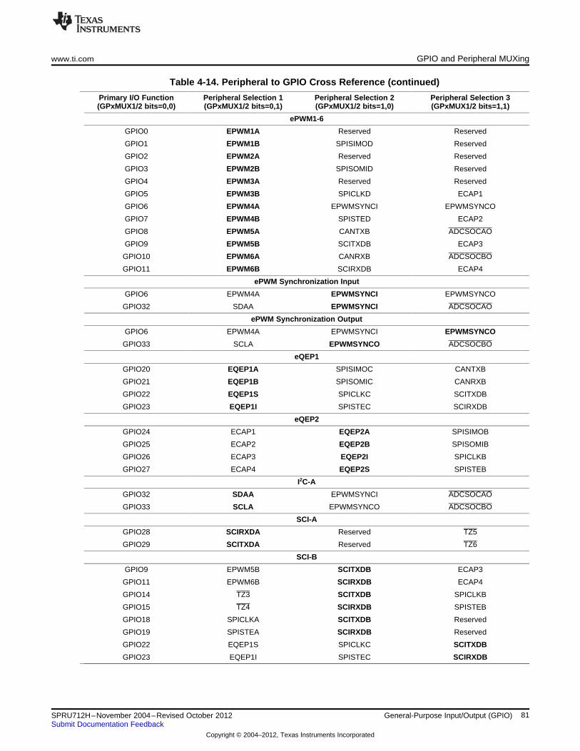
www.ti.com GPIO and Peripheral MUXing
Table 4-14. Peripheral to GPIO Cross Reference (continued)
Primary I/O Function Peripheral Selection 1 Peripheral Selection 2 Peripheral Selection 3(GPxMUX1/2 bits=0,0) (GPxMUX1/2 bits=0,1) (GPxMUX1/2 bits=1,0) (GPxMUX1/2 bits=1,1)
ePWM1-6
GPIO0 EPWM1A Reserved Reserved
GPIO1 EPWM1B SPISIMOD Reserved
GPIO2 EPWM2A Reserved Reserved
GPIO3 EPWM2B SPISOMID Reserved
GPIO4 EPWM3A Reserved Reserved
GPIO5 EPWM3B SPICLKD ECAP1
GPIO6 EPWM4A EPWMSYNCI EPWMSYNCO
GPIO7 EPWM4B SPISTED ECAP2
GPIO8 EPWM5A CANTXB ADCSOCAO
GPIO9 EPWM5B SCITXDB ECAP3
GPIO10 EPWM6A CANRXB ADCSOCBO
GPIO11 EPWM6B SCIRXDB ECAP4
ePWM Synchronization Input
GPIO6 EPWM4A EPWMSYNCI EPWMSYNCO
GPIO32 SDAA EPWMSYNCI ADCSOCAO
ePWM Synchronization Output
GPIO6 EPWM4A EPWMSYNCI EPWMSYNCO
GPIO33 SCLA EPWMSYNCO ADCSOCBO
eQEP1
GPIO20 EQEP1A SPISIMOC CANTXB
GPIO21 EQEP1B SPISOMIC CANRXB
GPIO22 EQEP1S SPICLKC SCITXDB
GPIO23 EQEP1I SPISTEC SCIRXDB
eQEP2
GPIO24 ECAP1 EQEP2A SPISIMOB
GPIO25 ECAP2 EQEP2B SPISOMIB
GPIO26 ECAP3 EQEP2I SPICLKB
GPIO27 ECAP4 EQEP2S SPISTEB
I2C-A
GPIO32 SDAA EPWMSYNCI ADCSOCAO
GPIO33 SCLA EPWMSYNCO ADCSOCBO
SCI-A
GPIO28 SCIRXDA Reserved TZ5
GPIO29 SCITXDA Reserved TZ6
SCI-B
GPIO9 EPWM5B SCITXDB ECAP3
GPIO11 EPWM6B SCIRXDB ECAP4
GPIO14 TZ3 SCITXDB SPICLKB
GPIO15 TZ4 SCIRXDB SPISTEB
GPIO18 SPICLKA SCITXDB Reserved
GPIO19 SPISTEA SCIRXDB Reserved
GPIO22 EQEP1S SPICLKC SCITXDB
GPIO23 EQEP1I SPISTEC SCIRXDB
81SPRU712H–November 2004–Revised October 2012 General-Purpose Input/Output (GPIO)Submit Documentation Feedback
Copyright © 2004–2012, Texas Instruments Incorporated

GPIO and Peripheral MUXing www.ti.com
Table 4-14. Peripheral to GPIO Cross Reference (continued)
Primary I/O Function Peripheral Selection 1 Peripheral Selection 2 Peripheral Selection 3(GPxMUX1/2 bits=0,0) (GPxMUX1/2 bits=0,1) (GPxMUX1/2 bits=1,0) (GPxMUX1/2 bits=1,1)
SPI-A
GPIO16 SPISIMOA CANTXB TZ5
GPIO17 SPISOMIA CANRXB TZ6
GPIO18 SPICLKA SCITXDB Reserved
GPIO19 SPISTEA SCIRXDB Reserved
SPI-B
GPIO12 TZ1 CANTXB SPISIMOB
GPIO13 TZ2 CANRXB SPISOMIB
GPIO14 TZ3 SCITXDB SPICLKB
GPIO15 TZ4 SCIRXDB SPISTEB
GPIO24 ECAP1 EQEP2A SPISIMOB
GPIO25 ECAP2 EQEP2B SPISOMIB
GPIO26 ECAP3 EQEP2I SPICLKB
GPIO27 ECAP4 EQEP2S SPISTEB
SPI-C
GPIO20 EQEP1A SPISIMOC CANTXB
GPIO21 EQEP1B SPISOMIC CANRXB
GPIO22 EQEP1S SPICLKC SCITXDB
GPIO23 EQEP1I SPISTEC SCIRXDB
SPI-D
GPIO1 EPWM1B SPISIMOD Reserved
GPIO3 EPWM2B SPISOMID Reserved
GPIO5 EPWM3B SPICLKD ECAP1
GPIO7 EPWM4B SPISTED ECAP2
Trip Zones 1-6
GPIO12 TZ1 CANTXB SPISIMOB
GPIO13 TZ2 CANRXB SPISOMIB
GPIO14 TZ3 SCITXDB SPICLKB
GPIO15 TZ4 SCIRXDB SPISTEB
GPIO16 SPISIMOA CANTXB TZ5
GPIO17 SPISOMIA CANRXB TZ6
GPIO28 SCIRXDA Reserved TZ5
GPIO29 SCITXDA Reserved TZ6
82 General-Purpose Input/Output (GPIO) SPRU712H–November 2004–Revised October 2012Submit Documentation Feedback
Copyright © 2004–2012, Texas Instruments Incorporated

www.ti.com Register Bit Definitions
4.6 Register Bit Definitions
Figure 4-4. GPIO Port A MUX 1 (GPAMUX1) Register31 30 29 28 27 26 25 24 23 22 21 20 19 18 17 16
GPIO15 GPIO14 GPIO13 GPIO12 GPIO11 GPIO10 GPIO9 GPIO8
R/W-0 R/W-0 R/W-0 R/W-0 R/W-0 R/W-0 R/W-0 R/W-0
15 14 13 12 11 10 9 8 7 6 5 4 3 2 1 0
GPIO7 GPIO6 GPIO5 GPIO4 GPIO3 GPIO2 GPIO1 GPIO0
R/W-0 R/W-0 R/W-0 R/W-0 R/W-0 R/W-0 R/W-0 R/W-0
LEGEND- R/W = Read/Write; R = Read only; -n = value after reset
Table 4-15. GPIO Port A MUX 1 (GPAMUX1) Register Field Descriptions
Bits Field Value Description (1)
31-30 GPIO15 Configure the GPIO15 pin as:
00 GPIO15 (I/O), General purpose I/O 15 (default)
01 • For 28044 device:
– If GPAMCFG[EPWMMODE] = 0,0 then TZ4 (I), Trip zone 4
– If GPAMCFG[EPWMMODE] = 1,1 then EPWM16A (O), ePWM16 output A.• All other devices: TZ4 (I), Trip zone 4
10 SCIRXDB (I), SCI-B receive.This option is reserved on devices that do not have an SCI-B port. (2)
11 SPISTEB (I/O), SPI-B transmit enable.This option is reserved on devices that do not have an SPI-B port. (2)
29-28 GPIO14 Configure the GPIO14 pin as:
00 GPIO14 (I/O), General purpose I/O 14 (default)
01 • For 28044 device:
– If GPAMCFG[EPWMMODE] = 0,0 then TZ3 (I), Trip zone 3
– If GPAMCFG[EPWMMODE] = 1,1 then EPWM15A (O), ePWM15 output A.• All other devices: TZ3 (I), Trip zone 3
10 SCITXDB (O), SCI-B transmit.This option is reserved on devices that do not have a SCI-B port. (2)
11 SPICLKB (I/O), SPI-B clock inThis option is reserved on devices that do not have a SPI-B port. (2)
27-26 GPIO13 Configure the GPIO13 pin as:
00 GPIO13 (I/O), General purpose I/O 13 (default)
01 • For 28044 device:
– If GPAMCFG[EPWMMODE] = 0,0 then TZ2 (I), Trip zone 2
– If GPAMCFG[EPWMMODE] = 1,1 then EPWM14A (O), ePWM14 output A.• All other devices: TZ2 (I), Trip zone 2
10 CANRXB (I), eCAN-B receive.This option is reserved on devices that do not have an eCAN-B port. (2)
11 SPISOMIB (I/O) SPI-B slave-out, master-inThis option is reserved on devices that do not have a SPI-B port. (2)
(1) This register is EALLOW protected. See Section 5.2 for more information.(2) If reserved configurations are selected, then the state of the pin will be undefined and the pin may be driven. These selections
are reserved for future expansion and should not be used.
83SPRU712H–November 2004–Revised October 2012 General-Purpose Input/Output (GPIO)Submit Documentation Feedback
Copyright © 2004–2012, Texas Instruments Incorporated

Register Bit Definitions www.ti.com
Table 4-15. GPIO Port A MUX 1 (GPAMUX1) Register Field Descriptions (continued)
Bits Field Value Description (1)
25-24 GPIO12 Configure the GPIO12 pin as:
00 GPIO12 (I/O), General purpose I/O 12 (default)
01 • For 28044 device:
– If GPAMCFG[EPWMMODE] = 0,0 then TZ1 (I), Trip zone 1
– If GPAMCFG[EPWMMODE] = 1,1 then EPWM12A (O), ePWM12 output A.• All other devices: TZ1 (I), Trip zone 1
10 CANTXB (O), eCAN-B transmit.This option is reserved on devices that do not have an eCAN-B port. (2)
11 SPISIMOB (I/O), SPI-B slave-in, master-outThis option is reserved on devices that do not have a SPI-B port. (2)
23-22 GPIO11 Configure the GPIO11 pin as:
00 GPIO11 (I/O), General purpose I/O 11 (default)
01 • For 28044 device:
– If GPAMCFG[EPWMMODE] = 0,0 then EPWM6B (O), ePWM 6 output B.
– If GPAMCFG[EPWMMODE] = 1,1 then EPWM12A (O), ePWM12 output A.• All other devices: EPWM6B (O), ePWM 6 output B.
This option is reserved on devices that do not have ePWM-6. (2)
10 SCIRXDB (I), SCI-B receive.This option is reserved on devices that do not have a SCI-B port. (2)
11 ECAP4 (I/O), eCAP4.This option is reserved on devices that do not have an eCAP4. (2)
21-20 GPIO10 Configure the GPIO10 pin as:
00 GPIO10 (I/O), General purpose I/O 10 (default)
01 • For 28044 device:
– If GPAMCFG[EPWMMODE] = 0,0 then EPWM6A (O), ePWM6 output A.
– If GPAMCFG[EPWMMODE] = 1,1 then EPWM11A (O), ePWM11 output A.• All other devices: EPWM6A (O), ePWM6 output A.
This option is reserved on devices that do not have ePWM-6. (2)
10 CANRXB (I), eCAN-B receive.This option is reserved on devices that do not have an eCAN-B port. (2)
11 ADCSOCBO (O), ADC Start of conversion B
19-18 GPIO9 Configure the GPIO9 pin as: (3)
00 GPIO9 (I/O) , General purpose I/O 9 (default)
01 • For 28044 device:
– If GPAMCFG[EPWMMODE] = 0,0 then EPWM5B (O), ePWM5 output B.
– If GPAMCFG[EPWMMODE] = 1,1 then EPWM10A (O), ePWM10 output A.• All other devices: EPWM5B (O), ePWM5 output B.
This option is reserved on devices that do not have ePWM-5. (4)
10 SCITXDB (O), SCI-B transmit.This option is reserved on devices that do not have a SCI-B port. (4)
11 ECAP3 (I/O), eCAP3
(3) This register is EALLOW protected. See Section 5.2 for more information.(4) If reserved configurations are selected, then the state of the pin will be undefined and the pin may be driven. These selections
are reserved for future expansion and should not be used.
84 General-Purpose Input/Output (GPIO) SPRU712H–November 2004–Revised October 2012Submit Documentation Feedback
Copyright © 2004–2012, Texas Instruments Incorporated

www.ti.com Register Bit Definitions
Table 4-15. GPIO Port A MUX 1 (GPAMUX1) Register Field Descriptions (continued)
Bits Field Value Description (1)
17-16 GPIO8 Configure the GPIO8 pin as:
00 GPIO8 (I/O), General purpose I/O 8 (default)
01 • For 28044 device:
– If GPAMCFG[EPWMMODE] = 0,0 then EPWM5A (O), ePWM5 output A.
– If GPAMCFG[EPWMMODE] = 1,1 then EPWM9A (O), ePWM9 output A.• All other devices: EPWM5A (O), ePWM5 output A.
This option is reserved on devices that do not have ePWM-5. (4)
10 CANTXB (O), eCAN-B transmit.This option is reserved on devices that do not have an eCAN-B port. (4)
11 ADCSOCAO (O), ADC Start of conversion A
15-14 GPIO7 Configure the GPIO7 pin as:
00 GPIO7 (I/O), General purpose I/O 7 (default)
01 • For 28044 device:
– If GPAMCFG[EPWMMODE] = 0,0 then EPWM4B (O), ePWM4 output B.
– If GPAMCFG[EPWMMODE] = 1,1 then EPWM8A (O), ePWM8 output A• All other devices: EPWM4B (O), ePWM4 output B.
This option is reserved on devices that do not have ePWM-4. (4)
10 SPISTED (I/O), SPI-D transmit enable.This option is reserved on devices that do not have a SPI-D port. (4)
11 ECAP2 (I/O), eCAP2This option is reserved on devices that do not have an eCAP2. (4)
13-12 GPIO6 Configure the GPIO6 pin as:
00 GPIO6 (I/O), General purpose I/O 6 (default)
01 • For 28044 device:
– If GPAMCFG[EPWMMODE] = 0,0 then EPWM4A (O), ePWM4 output A.
– If GPAMCFG[EPWMMODE] = 1,1 then EPWM7A (O), ePWM7 output A• All other devices: EPWM4A (O), ePWM4 output A.
This option is reserved on devices that do not have ePWM-4. (4)
10 EPWMSYNCI (I), ePWM Synch-in
11 EPWMSYNCO (O), ePWM Synch-out
11-10 GPIO5 Configure the GPIO5 pin as:
00 GPIO5 (I/O), General purpose I/O 5 (default)
01 • For 28044 device:
– If GPAMCFG[EPWMMODE] = 0,0 then EPWM3B (O), ePWM3 output B
– If GPAMCFG[EPWMMODE] = 1,1 then EPWM6A (O), ePWM6 output A• All other devices: EPWM3B (O), ePWM3 output B
10 SPICLKD (I/O), SPI-D clock.This option is reserved on devices that do not have SPI-D. (4)
11 ECAP1 (I/O), eCAP1This option is reserved on devices that do not have an eCAP1. (4)
9-8 GPIO4 Configure the GPIO4 pin as:
00 GPIO4 (I/O), General purpose I/O 4 (default)
01 • For 28044 device:
– If GPAMCFG[EPWMMODE] = 0,0 then EPWM3A (O), ePWM3 output A
– If GPAMCFG[EPWMMODE] = 1,1 then EPWM5A (O), ePWM5 output A• All other devices: EPWM3A (O), ePWM3 output A
10 Reserved (5)
11 Reserved (5)
(5) If reserved configurations are selected, then the state of the pin will be undefined and the pin may be driven. These selectionsare reserved for future expansion and should not be used.
85SPRU712H–November 2004–Revised October 2012 General-Purpose Input/Output (GPIO)Submit Documentation Feedback
Copyright © 2004–2012, Texas Instruments Incorporated

Register Bit Definitions www.ti.com
Table 4-15. GPIO Port A MUX 1 (GPAMUX1) Register Field Descriptions (continued)
Bits Field Value Description (1)
7-6 GPIO3 Configure the GPIO3 pin as:
00 GPIO3 (I/O), General purpose I/O 3 (default)
01 • For 28044 device:
– If GPAMCFG[EPWMMODE] = 0,0 then EPWM2B (O), ePWM2 output B
– If GPAMCFG[EPWMMODE] = 1,1 then EPWM4A (O), ePWM4 output A• All other devices: EPWM2B (O), ePWM2 output B
10 SPISOMID (I/O), SPI-D slave-out, master-in.This option is reserved on devices that do not have a SPI-D. (5)
11 Reserved (5)
5-4 GPIO2 Configure the GPIO2 pin as:
00 GPIO2 (I/O) General purpose I/O 2 (default)
01 • For 28044 device:
– If GPAMCFG[EPWMMODE] = 0,0 then EPWM2A (O), ePWM2 output A
– If GPAMCFG[EPWMMODE] = 1,1 then EPWM3A (O), ePWM3 output A• All other devices: EPWM2A (O), ePWM2 output A
10 Reserved (5)
11 Reserved (5)
3-2 GPIO1 Configure the GPIO1 pin as:
00 GPIO1 (I/O) General purpose I/O 1 (default)
01 • For 28044 device:
– If GPAMCFG[EPWMMODE] = 0,0 then EPWM1B (O), ePWM1 output B
– If GPAMCFG[EPWMMODE] = 1,1 then EPWM2A (O), ePWM2 output A• All other devices: EPWM1B (O), ePWM1 output B
10 SPISIMOD (I/O) SPI-D slave-in, master-out.This option is reserved on devices that do not have a SPI-D. (6)
11 Reserved (6)
1-0 GPIO0 Configure the GPIO0 pin as:
00 GPIO0 (I/O), General purpose I/O 0 (default)
01 • For 28044 device:
– If GPAMCFG[EPWMMODE] = 0,0 then EPWM1A (O), ePWM1 output A
– If GPAMCFG[EPWMMODE] = 1,1 then EPWM1A (O), ePWM1 output A• All other devices: EPWM1A (O), ePWM1 output A
10 Reserved (6)
11 Reserved (6)
(6) If reserved configurations are selected, then the state of the pin will be undefined and the pin may be driven. These selectionsare reserved for future expansion and should not be used.
Figure 4-5. GPIO Port A MUX 2 (GPAMUX2) Register31 30 29 28 27 26 25 24 23 22 21 20 19 18 17 16
GPIO31 GPIO30 GPIO29 GPIO128 GPIO27 GPIO26 GPIO25 GPIO24
R/W-0 R/W-0 R/W-0 R/W-0 R/W-0 R/W-0 R/W-0 R/W-0
15 14 13 12 11 10 9 8 7 6 5 4 3 2 1 0
GPIO23 GPIO22 GPIO21 GPIO20 GPIO19 GPIO18 GPIO17 GPIO16
R/W-0 R/W-0 R/W-0 R/W-0 R/W-0 R/W-0 R/W-0 R/W-0
LEGEND: R/W = Read/Write; R = Read only; -n = value after reset
86 General-Purpose Input/Output (GPIO) SPRU712H–November 2004–Revised October 2012Submit Documentation Feedback
Copyright © 2004–2012, Texas Instruments Incorporated

www.ti.com Register Bit Definitions
Table 4-16. GPIO Port A MUX 2 (GPAMUX2) Register Field Descriptions
Bits Field Value Description (1)
31-30 GPIO31 Configure the GPIO31 pin as:
00 GPIO31 (I/O) General purpose I/O 31 (default)
01 CANTXA (O), eCAN-A transmitThis option is reserved on devices that do not have an eCAN-A port. (2)
10 Reserved (2)
11 On 28044 device: TZ4 (I), Trip zone 4On all other devices: Reserved (2)
29-28 GPIO30 Configure the GPIO30 pin as:
00 GPIO30 (I/O) General purpose I/O 30 (default)
01 CANRXA (I), eCAN-A receiveThis option is reserved on devices that do not have an eCAN-A port. (2)
10 Reserved (2)
11 On 28044 device: TZ3 (I), Trip zone 3On all other devices: Reserved (2)
27-26 GPIO29 Configure the GPIO29 pin as:
00 GPIO29 (I/O) General purpose I/O 29 (default)
01 SCITXDA (O), SCI-A transmit.
10 Reserved (2)
11 TZ6 (I), trip zone 6
25-24 GPIO28 Configure the GPIO28 pin as:
00 GPIO28 (I/O) General purpose I/O 28 (default)
01 SCIRXDA (I), SCI-A receive
10 Reserved (2)
11 TZ5 (I), trip zone 5
23-22 GPIO27 Configure the GPIO27 pin as:
00 GPIO27 (I/O), General purpose I/O 27 (default)
01 ECAP4 (I/O), eCAP4.This option is reserved on devices that do not have an eCAP4. (2)
10 EQEP2S (I/O), eQEP2 strobe.This option is reserved on devices that do not have an eQEP2. (2)
11 SPISTEB (I/O), SPI-B transmit enableThis option is reserved on devices that do not have a SPI-B port. (2)
21-20 GPIO26 Configure the GPIO26 pin as:
00 GPIO26 (I/O), General purpose I/O 26 (default)
01 ECAP3 (I/O), eCAP3.This option is reserved on devices that do not have an eCAP3. (2)
10 EQEP2I (I/O), eQEP2 index.This option is reserved on devices that do not have an eQEP2. (2)
11 SPICLKB (I/O), SPI-B clockThis option is reserved on devices that do not have an SPI-B port. (2)
19-18 GPIO25 Configure the GPIO25 pin as:
00 GPIO25 (I/O), General purpose I/O 25 (default)
01 ECAP2 (I/O), eCAP2.This option is reserved on devices that do not have an eCAP2. (2)
10 EQEP2B (I), eQEP2 input B.This option is reserved on devices that do not have an eQEP2. (2)
11 SPISOMIB (I/O), SPI-B slave-out, master-inThis option is reserved on devices that do not have a SPI-B port. (2)
(1) This register is EALLOW protected. See Section 5.2 for more information.(2) If reserved configurations are selected, then the state of the pin will be undefined and the pin may be driven. These selections
are reserved for future expansion and should not be used.
87SPRU712H–November 2004–Revised October 2012 General-Purpose Input/Output (GPIO)Submit Documentation Feedback
Copyright © 2004–2012, Texas Instruments Incorporated
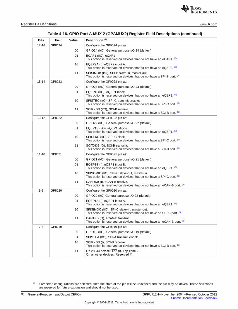
Register Bit Definitions www.ti.com
Table 4-16. GPIO Port A MUX 2 (GPAMUX2) Register Field Descriptions (continued)
Bits Field Value Description (1)
17-16 GPIO24 Configure the GPIO24 pin as:
00 GPIO24 (I/O), General purpose I/O 24 (default)
01 ECAP1 (I/O), eCAP1This option is reserved on devices that do not have an eCAP1. (2)
10 EQEP2A (I), eQEP2 input A.This option is reserved on devices that do not have an eQEP2. (2)
11 SPISIMOB (I/O), SPI-B slave-in, master-out.This option is reserved on devices that do not have a SPI-B port. (2)
15-14 GPIO23 Configure the GPIO23 pin as:
00 GPIO23 (I/O), General purpose I/O 23 (default)
01 EQEP1I (I/O), eQEP1 index.This option is reserved on devices that do not have an eQEP1. (2)
10 SPISTEC (I/O), SPI-C transmit enable.This option is reserved on devices that do not have a SPI-C port. (2)
11 SCIRXDB (I/O), SCI-B receive.This option is reserved on devices that do not have a SCI-B port. (2)
13-12 GPIO22 Configure the GPIO22 pin as:
00 GPIO22 (I/O), General purpose I/O 22 (default)
01 EQEP1S (I/O), eQEP1 strobe.This option is reserved on devices that do not have an eQEP1. (2)
10 SPICLKC (I/O), SPI-C clock.This option is reserved on devices that do not have a SPI-C port. (2)
11 SCITXDB (O), SCI-B transmit.This option is reserved on devices that do not have a SCI-B port. (2)
11-10 GPIO21 Configure the GPIO21 pin as:
00 GPIO21 (I/O), General purpose I/O 21 (default)
01 EQEP1B (I), eQEP1 input B.This option is reserved on devices that do not have an eQEP1. (3)
10 SPISOMIC (I/O), SPI-C slave-out, master-in.This option is reserved on devices that do not have a SPI-C port. (3)
11 CANRXB (I), eCAN-B receive.This option is reserved on devices that do not have an eCAN-B port. (3)
9-8 GPIO20 Configure the GPIO20 pin as:
00 GPIO20 (I/O) General purpose I/O 22 (default)
01 EQEP1A (I), eQEP1 input A.This option is reserved on devices that do not have an eQEP1. (3)
10 SPISIMOC (I/O), SPI-C slave-in, master-out.This option is reserved on devices that do not have an SPI-C port. (3)
11 CANTXB (O), eCAN-B transmit.This option is reserved on devices that do not have an eCAN-B port. (3)
7-6 GPIO19 Configure the GPIO19 pin as:
00 GPIO19 (I/O), General purpose I/O 19 (default)
01 SPISTEA (I/O), SPI-A transmit enable.
10 SCIRXDB (I), SCI-B receive.This option is reserved on devices that do not have a SCI-B port. (3)
11 On 28044 device: TZ2 (I), Trip zone 2On all other devices: Reserved (3)
(3) If reserved configurations are selected, then the state of the pin will be undefined and the pin may be driven. These selectionsare reserved for future expansion and should not be used.
88 General-Purpose Input/Output (GPIO) SPRU712H–November 2004–Revised October 2012Submit Documentation Feedback
Copyright © 2004–2012, Texas Instruments Incorporated

www.ti.com Register Bit Definitions
Table 4-16. GPIO Port A MUX 2 (GPAMUX2) Register Field Descriptions (continued)
Bits Field Value Description (1)
5-4 GPIO18 Configure the GPIO18 pin as:
00 GPIO18 (I/O), General purpose I/O 18 (default)
01 SPICLKA (I/O), SPI-A clock
10 SCITXDB (O), SCI-B transmit.This option is reserved on devices that do not have an SCI-B port. (3)
11 On 28044 device: TZ1 (I), Trip zone 1On all other devices: Reserved (3)
3-2 GPIO17 Configure the GPIO17 pin as:
00 GPIO17 (I/O), General purpose I/O 17 (default)
01 SPISOMIA (I/O), SPI-A slave-out, master-in
10 CANRXB (I), eCAN-B receive.This option is reserved on devices that do not have an eCAN-B port. (3)
11 TZ6 (I), Trip zone 6
1-0 GPIO16 Configure the GPIO16 pin as:
00 GPIO16 (I/O), General purpose I/O 16 (default)
01 SPISIMOA (I/O), SPI-A slave-in, master-out
10 CANTXB (O), eCAN-B transmit.This option is reserved on devices that do not have an eCAN-B port. (3)
11 TZ5 (I), Trip zone 5
Figure 4-6. GPIO Port B MUX 1 (GPBMUX1) Register31 6 5 4 3 2 1 0
Reserved GPIO34 GPIO33 GPIO32
R-0 R/W-0 R/W-0 R/W-0
LEGEND: R/W = Read/Write; R = Read only; -n = value after reset
Table 4-17. GPIO Port B MUX 1 (GPBMUX1) Register Field Descriptions
Bits Field Value Description (1)
31-6 Reserved Reserved
5-4 GPIO34 Configure the GPIO34 pin as:
00 GPIO34 (I/O), General purpose I/O 34 (default)
01 Reserved (2)
10 Reserved (2)
11 Reserved (2)
3-2 GPIO33 Configure the GPIO33 pin as:
00 GPIO33 (I/O), General purpose I/O 33 (default)
01 SCLA (I/O), I2C clock
10 EPWMSYNCO (O), ePWM synchronization output
11 ADCSOCBO (O)
1-0 GPIO32 Configure the GPIO32 pin as:
00 GPIO32 (I/O), General purpose I/O 32 (default)
01 SDAA(I/O), I2C data
10 EWPMSYNCI (I), ePWM ePWM synchronization input
11 ADCSOCAO (O), ADC start of conversion A(1) This register is EALLOW protected. See Section 5.2 for more information.(2) If reserved configurations are selected, then the state of the pin will be undefined and the pin may be driven. These selections
are reserved for future expansion and should not be used.
89SPRU712H–November 2004–Revised October 2012 General-Purpose Input/Output (GPIO)Submit Documentation Feedback
Copyright © 2004–2012, Texas Instruments Incorporated

Register Bit Definitions www.ti.com
90 General-Purpose Input/Output (GPIO) SPRU712H–November 2004–Revised October 2012Submit Documentation Feedback
Copyright © 2004–2012, Texas Instruments Incorporated
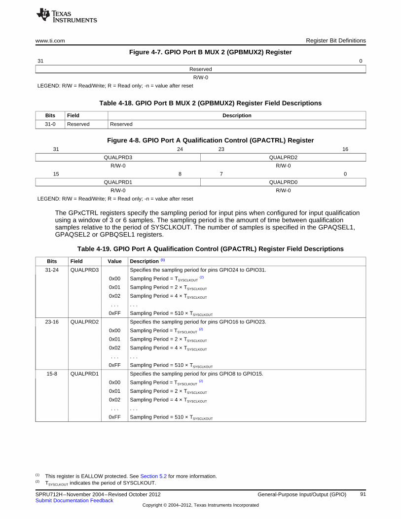
www.ti.com Register Bit Definitions
Figure 4-7. GPIO Port B MUX 2 (GPBMUX2) Register31 0
Reserved
R/W-0
LEGEND: R/W = Read/Write; R = Read only; -n = value after reset
Table 4-18. GPIO Port B MUX 2 (GPBMUX2) Register Field Descriptions
Bits Field Description
31-0 Reserved Reserved
Figure 4-8. GPIO Port A Qualification Control (GPACTRL) Register31 24 23 16
QUALPRD3 QUALPRD2
R/W-0 R/W-0
15 8 7 0
QUALPRD1 QUALPRD0
R/W-0 R/W-0
LEGEND: R/W = Read/Write; R = Read only; -n = value after reset
The GPxCTRL registers specify the sampling period for input pins when configured for input qualificationusing a window of 3 or 6 samples. The sampling period is the amount of time between qualificationsamples relative to the period of SYSCLKOUT. The number of samples is specified in the GPAQSEL1,GPAQSEL2 or GPBQSEL1 registers.
Table 4-19. GPIO Port A Qualification Control (GPACTRL) Register Field Descriptions
Bits Field Value Description (1)
31-24 QUALPRD3 Specifies the sampling period for pins GPIO24 to GPIO31.
0x00 Sampling Period = TSYSCLKOUT(2)
0x01 Sampling Period = 2 × TSYSCLKOUT
0x02 Sampling Period = 4 × TSYSCLKOUT
. . . . . .
0xFF Sampling Period = 510 × TSYSCLKOUT
23-16 QUALPRD2 Specifies the sampling period for pins GPIO16 to GPIO23.
0x00 Sampling Period = TSYSCLKOUT(2)
0x01 Sampling Period = 2 × TSYSCLKOUT
0x02 Sampling Period = 4 × TSYSCLKOUT
. . . . . .
0xFF Sampling Period = 510 × TSYSCLKOUT
15-8 QUALPRD1 Specifies the sampling period for pins GPIO8 to GPIO15.
0x00 Sampling Period = TSYSCLKOUT(2)
0x01 Sampling Period = 2 × TSYSCLKOUT
0x02 Sampling Period = 4 × TSYSCLKOUT
. . . . . .
0xFF Sampling Period = 510 × TSYSCLKOUT
(1) This register is EALLOW protected. See Section 5.2 for more information.(2) TSYSCLKOUT indicates the period of SYSCLKOUT.
91SPRU712H–November 2004–Revised October 2012 General-Purpose Input/Output (GPIO)Submit Documentation Feedback
Copyright © 2004–2012, Texas Instruments Incorporated

Register Bit Definitions www.ti.com
Table 4-19. GPIO Port A Qualification Control (GPACTRL) Register Field Descriptions (continued)
Bits Field Value Description (1)
7-0 QUALPRD0 Specifies the sampling period for pins GPIO0 to GPIO7.
0x00 Sampling Period = TSYSCLKOUT(2)
0x01 Sampling Period = 2 × TSYSCLKOUT
0x02 Sampling Period = 4 × TSYSCLKOUT
. . . . . .
0xFF Sampling Period = 510 × TSYSCLKOUT
Figure 4-9. GPIO Port B Qualification Control (GPBCTRL) Register31 8 7 0
Reserved QUALPRD0
R-0 R/W-0
LEGEND: R/W = Read/Write; R = Read only; -n = value after reset
Table 4-20. GPIO Port B Input Qualification Control (GPBCTRL) Register Field Descriptions
Bits Field Value Description (1)
31-8 Reserved Reserved
7-0 QUALPRD0 Specifies the qualification sampling period for pins GPIO32 to GPIO34.
0x00 Sampling Period = TSYSCLKOUT(2)
0x01 Sampling Period = 2 × TSYSCLKOUT
0x02 Sampling Period = 4 × TSYSCLKOUT
. . . . . .
0xFF Sampling Period = 510 × TSYSCLKOUT
(1) This register is EALLOW protected. See Section 5.2 for more information.(2) TSYSCLKOUT indicates the period of SYSCLKOUT.
Figure 4-10. GPIO Port A Qualification Select 1 (GPAQSEL1) Register31 30 29 28 27 26 25 24 23 22 21 20 19 18 17 16
GPIO15 GPIO14 GPIO13 GPIO12 GPIO11 GPIO10 GPIO9 GPIO8
R/W-0 R/W-0 R/W-0 R/W-0 R/W-0 R/W-0 R/W-0 R/W-0
15 14 13 12 11 10 9 8 7 6 5 4 3 2 1 0
GPIO7 GPIO6 GPIO5 GPIO4 GPIO3 GPIO2 GPIO1 GPIO0
R/W-0 R/W-0 R/W-0 R/W-0 R/W-0 R/W-0 R/W-0 R/W-0
LEGEND: R/W = Read/Write; R = Read only; -n = value after reset
Table 4-21. GPIO Port A Qualification Select 1 (GPAQSEL1) Register Field Descriptions
Bits Field Value Description (1)
31-0 GPIO15-GPIO0 Select input qualification type for GPIO0 to GPIO15. The input qualification of each GPIOinput is controlled by two bits as shown in Figure 4-10.
00 Synchronize to SYSCLKOUT only. Valid for both peripheral and GPIO pins.
01 Qualification using 3 samples. Valid for pins configured as GPIO or a peripheral function.The time between samples is specified in the GPACTRL register.
10 Qualification using 6 samples. Valid for pins configured as GPIO or a peripheral function.The time between samples is specified in the GPACTRL register.
11 Asynchronous. (no synchronization or qualification). This option applies to pins configuredas peripherals only. If the pin is configured as a GPIO input, then this option is the same as0,0 or synchronize to SYSCLKOUT.
(1) This register is EALLOW protected. See Section 5.2 for more information.
92 General-Purpose Input/Output (GPIO) SPRU712H–November 2004–Revised October 2012Submit Documentation Feedback
Copyright © 2004–2012, Texas Instruments Incorporated

www.ti.com Register Bit Definitions
Figure 4-11. GPIO Port A Qualification Select 2 (GPAQSEL2) Register31 30 29 28 27 26 25 24 23 22 21 20 19 18 17 16
GPIO31 GPIO30 GPIO29 GPIO28 GPIO27 GPIO26 GPIO25 GPIO24
R/W-0 R/W-0 R/W-0 R/W-0 R/W-0 R/W-0 R/W-0 R/W-0
15 14 13 12 11 10 9 8 7 6 5 4 3 2 1 0
GPIO23 GPIO22 GPIO21 GPIO20 GPIO19 GPIO18 GPIO17 GPIO16
R/W-0 R/W-0 R/W-0 R/W-0 R/W-0 R/W-0 R/W-0 R/W-0
LEGEND: R/W = Read/Write; R = Read only; -n = value after reset
Table 4-22. GPIO Port A Qualification Select 2 (GPAQSEL2) Register Field Descriptions
Bits Field Value Description (1)
31-0 GPIO31-GPIO16 Select input qualification type for GPIO16 to GPIO31. The input qualification of each GPIOinput is controlled by two bits as shown in Figure 4-11.
00 Synchronize to SYSCLKOUT only. Valid for both peripheral and GPIO pins.
01 Qualification using 3 samples. Valid for pins configured as GPIO or a peripheral function. Thetime between samples is specified in the GPACTRL register.
10 Qualification using 6 samples. Valid for pins configured as GPIO or a peripheral function. Thetime between samples is specified in the GPACTRL register.
11 Asynchronous. (no synchronization or qualification). This option applies to pins configured asperipherals only. If the pin is configured as a GPIO input, then this option is the same as 0,0or synchronize to SYSCLKOUT.
(1) This register is EALLOW protected. See Section 5.2 for more information.
Figure 4-12. GPIO Port B Qualification Select 1 (GPBQSEL1) Register31 6 5 4 3 2 1 0
Reserved GPIO34 GPIO33 GPIO32
R-0 R/W-0 R/W-0 R/W-0
LEGEND: R/W = Read/Write; R = Read only; -n = value after reset
Table 4-23. GPIO Port B Qualification Select 1 (GPBQSEL1) Register Field Descriptions
Bits Field Value Description (1)
31-6 Reserved
5-0 GPIO34-GPIO32 Select input qualification type for GPIO32 to GPIO34. The input qualification of each GPIOinput is controlled by two bits as shown in Figure 4-12.
00 Synchronize to SYSCLKOUT only. Valid for both peripheral and GPIO pins.
01 Qualification using 3 samples. Valid for pins configured as GPIO or a peripheral function.The time between samples is specified in the GPBCTRL register.
10 Qualification using 6 samples. Valid for pins configured as GPIO or a peripheral function.The time between samples is specified in the GPBCTRL register.
11 Asynchronous. (no synchronization or qualification). This option applies to pins configuredas peripherals only. If the pin is configured as a GPIO input, then this option is the sameas 0,0 or sync to SYSCLKOUT.
(1) This register is EALLOW protected. See Section 5.2 for more information.
Table 4-24. GPIO Port B Qualification Select 2 (GPBQSEL2) Register Field Descriptions
Bits Field Description
31-0 Reserved Reserved for future expansion
The GPADIR and GPBDIR registers control the direction of the pins when they are configured as a GPIOin the appropriate MUX register. The direction register has no effect on pins configured as peripheralfunctions.
93SPRU712H–November 2004–Revised October 2012 General-Purpose Input/Output (GPIO)Submit Documentation Feedback
Copyright © 2004–2012, Texas Instruments Incorporated

Register Bit Definitions www.ti.com
Figure 4-13. GPIO Port A Direction (GPADIR) Register31 30 29 28 27 26 25 24
GPIO31 GPIO30 GPIO29 GPIO28 GPIO27 GPIO26 GPIO25 GPIO24
R/W-0 R/W-0 R/W-0 R/W-0 R/W-0 R/W-0 R/W-0 R/W-0
23 22 21 20 19 18 17 16
GPIO23 GPIO22 GPIO21 GPIO20 GPIO19 GPIO18 GPIO17 GPIO16
R/W-0 R/W-0 R/W-0 R/W-0 R/W-0 R/W-0 R/W-0 R/W-0
15 14 13 12 11 10 9 8
GPIO15 GPIO14 GPIO13 GPIO12 GPIO11 GPIO10 GPIO9 GPIO8
R/W-0 R/W-0 R/W-0 R/W-0 R/W-0 R/W-0 R/W-0 R/W-0
7 6 5 4 3 2 1 0
GPIO7 GPIO6 GPIO5 GPIO4 GPIO3 GPIO2 GPIO1 GPIO0
R/W-0 R/W-0 R/W-0 R/W-0 R/W-0 R/W-0 R/W-0 R/W-0
LEGEND: R/W = Read/Write; R = Read only; -n = value after reset
Table 4-25. GPIO Port A Direction (GPADIR) Register Field Descriptions
Bits Field Value Description (1)
31-0 GPIO31-GPIO0 Controls direction of GPIO Port A pins when the specified pin is configured as a GPIO in theappropriate GPAMUX1 or GPAMUX2 register.
0 Configures the GPIO pin as an input. (default)
1 Configures the GPIO pin as an output
The value currently in the GPADAT output latch is driven on the pin. To initialize the GPADATlatch prior to changing the pin from an input to an output, use the GPASET, GPACLEAR, andGPATOGGLE registers.
(1) This register is EALLOW protected. See Section 5.2 for more information.
Figure 4-14. GPIO Port B Direction (GPBDIR) Register31 3 2 1 0
Reserved GPIO34 GPIO33 GPIO32
R-0 R/W-0 R/W-0 R/W-0
LEGEND: R/W = Read/Write; R = Read only; -n = value after reset
Table 4-26. GPIO Port B Direction (GPBDIR) Register Field Descriptions
Bits Field Value Description (1)
31-3 Reserved
2-0 GPIO34-GPIO32 Controls the direction of GPIO Port B pins (input or output) when the specified pin isconfigured as a GPIO in the appropriate GPBMUX1 or GPBMUX2 register.
0 Configures the GPIO pin as an input. (default)
1 Configures the GPIO pin as an output
The value currently in the GPBDAT output latch is driven on the pin. To initialize the GPBDATlatch prior to changing the pin from an input to an output, use the GPBSET, GPBCLEAR, andGPBTOGGLE registers.
(1) This register is EALLOW protected. See Section 5.2 for more information.
94 General-Purpose Input/Output (GPIO) SPRU712H–November 2004–Revised October 2012Submit Documentation Feedback
Copyright © 2004–2012, Texas Instruments Incorporated

www.ti.com Register Bit Definitions
The pullup disable (GPxPUD) registers allow you to specify which pins should have an internal pullupresister enabled. The internal pullups on the pins that can be configured as ePWM outputs(GPIO0-GPIO11) are all disabled asynchronously when the external reset signal (XRS) is low. The internal pullupson all other pins are enabled on reset. When coming out of reset, the pullups remain in their default stateuntil you enable or disable them selectively in software by writing to this register. The pullup configurationapplies both to pins configured as I/O and those configured as peripheral functions.
Figure 4-15. GPIO Port A Pullup Disable (GPAPUD) Registers31 30 29 28 27 26 25 24
GPIO31 GPIO30 GPIO29 GPIO28 GPIO27 GPIO26 GPIO25 GPIO24
R/W-0 R/W-0 R/W-0 R/W-0 R/W-0 R/W-0 R/W-0 R/W-0
23 22 21 20 19 18 17 16
GPIO23 GPIO22 GPIO21 GPIO20 GPIO19 GPIO18 GPIO17 GPIO16
R/W-0 R/W-0 R/W-0 R/W-0 R/W-0 R/W-0 R/W-0 R/W-0
15 14 13 12 11 10 9 8
GPIO15(1) GPIO14(1) GPIO13(1) GPIO12(1) GPIO11 GPIO10 GPIO9 GPIO8
R/W-0 R/W-0 R/W-0 R/W-0 R/W-1 R/W-1 R/W-1 R/W-1
7 6 5 4 3 2 1 0
GPIO7 GPIO6 GPIO5 GPIO4 GPIO3 GPIO2 GPIO1 GPIO0
R/W-1 R/W-1 R/W-1 R/W-1 R/W-1 R/W-1 R/W-1 R/W-1
LEGEND: R/W = Read/Write; R = Read only; -n = value after reset
(1) On the F28044 device, GPIO12 - GPIO15 pull-ups are also disabled at reset.
Table 4-27. GPIO Port A Internal Pullup Disable (GPAPUD) Register Field Descriptions
Bits Field Value Description (1)
31-0 GPIO31-GPIO0 Configure the internal pullup resister on the selected GPIO Port A pin. Each GPIO pincorresponds to one bit in this register as shown in Figure 4-15.
0 Enable the internal pullup on the specified pin. (default for GPIO12-GPIO31)
1 Disable the internal pullup on the specified pin. (default for GPIO0-GPIO11)(1) This register is EALLOW protected. See Section 5.2 for more information.
Figure 4-16. GPIO Port B Pullup Disable (GPBPUD) Register31 6 5 4 3 2 1 0
Reserved Reserved Reserved GPIO35 GPIO34 GPIO33 GPIO32
R-0 R/W-0 R/W-1 R/W-1 R/W-0 R/W-0 R/W-0
LEGEND: R/W = Read/Write; R = Read only; -n = value after reset
Table 4-28. GPIO Port B Internal Pullup Disable (GPBPUD) Register Field Descriptions
Bits Field Value Description (1)
31-3 Reserved Reserved
2-0 GPIO35 (2)- Configure the internal pullup resister on the selected GPIO Port B pin. Each GPIO pinGPIO32 corresponds to one bit in this register as shown in Figure 4-16.
0 Enable the internal pullup on the specified pin. (default)
1 Disable the internal pullup on the specified pin.(1) This register is EALLOW protected. See Section 5.2 for more information.(2) GPIO35 signal is internally available, but not pinned out. The internal pullup for this signal is disabled upon reset. To minimize the
leakage currents in order to ensure that the low-power mode IDDIO current stays within the datasheet limits, this pullup has to beenabled by the user. i.e. bit 3 should be 0. Any write to GPBPUD should ensure bit 5 remains 0.
95SPRU712H–November 2004–Revised October 2012 General-Purpose Input/Output (GPIO)Submit Documentation Feedback
Copyright © 2004–2012, Texas Instruments Incorporated

Register Bit Definitions www.ti.com
The GPIO data registers indicate the current status of the GPIO pin, irrespective of which mode the pin isin. Writing to this register will set the respective GPIO pin high or low if the pin is enabled as a GPIOoutput, otherwise the value written is latched but ignored. The state of the output register latch will remainin its current state until the next write operation. A reset will clear all bits and latched values to zero. Thevalue read from the GPADAT and GPBDAT registers reflect the state of the pin (after qualification), notthe state of the output latch of the GPADAT or GPBDAT register.
Typically the DAT registers are used for reading the current state of the pins. To easily modify the outputlevel of the pin refer to the SET, CLEAR and TOGGLE registers.
Figure 4-17. GPIO Port A Data (GPADAT) Register31 30 29 28 27 26 25 24
GPIO31 GPIO30 GPIO29 GPIO28 GPIO27 GPIO26 GPIO25 GPIO24
R/W-x R/W-x R/W-x R/W-x R/W-x R/W-x R/W-x R/W-x
23 22 21 20 19 18 17 16
GPIO23 GPIO22 GPIO21 GPIO20 GPIO19 GPIO18 GPIO17 GPIO16
R/W-x R/W-x R/W-x R/W-x R/W-x R/W-x R/W-x R/W-x
15 14 13 12 11 10 9 8
GPIO15 GPIO14 GPIO13 GPIO12 GPIO11 GPIO10 GPIO9 GPIO8
R/W-x R/W-x R/W-x R/W-x R/W-x R/W-x R/W-x R/W-x
7 6 5 4 3 2 1 0
GPIO7 GPIO6 GPIO5 GPIO4 GPIO3 GPIO2 GPIO1 GPIO0
R/W-x R/W-x R/W-x R/W-x R/W-x R/W-x R/W-x R/W-x
LEGEND: R/W = Read/Write; R = Read only; -n = value after reset (1)
(1) x = The state of the GPADAT register is unknown after reset. It depends on the level of the pin after reset.
Table 4-29. GPIO Port A Data (GPADAT) Register Field Descriptions
Bits Field Value Description
31-0 GPIO31-GPIO0 Each bit corresponds to one GPIO port A pin (GPIO0-GPIO31) as shown in Figure 4-17.
0 Reading a 0 indicates that the state of the pin is currently low, irrespective of the mode the pin isconfigured for.
Writing a 0 will force an output of 0 if the pin is configured as a GPIO output in the appropriateGPAMUX1/2 and GPADIR registers; otherwise, the value is latched but not used to drive thepin.
1 Reading a 1 indicates that the state of the pin is currently high irrespective of the mode the pinis configured for.
Writing a 1will force an output of 1if the pin is configured as a GPIO output in the appropriateGPAMUX1/2 and GPADIR registers; otherwise, the value is latched but not used to drive thepin.
96 General-Purpose Input/Output (GPIO) SPRU712H–November 2004–Revised October 2012Submit Documentation Feedback
Copyright © 2004–2012, Texas Instruments Incorporated

www.ti.com Register Bit Definitions
Figure 4-18. GPIO Port B Data (GPBDAT) Register31 3 2 1 0
Reserved GPIO35 GPIO34 GPIO33 GPIO32
R-0 R/W-x R/W-x R/W-x R/W-x
LEGEND: R/W = Read/Write; R = Read only; -n = value after reset (1)
(1) x = The state of the GPBDAT register is unknown after reset. It depends on the level of the pin after reset.
Table 4-30. GPIO Port B Data (GPBDAT) Register Field Descriptions
Bit Field Value Description
31-3 Reserved Reserved
2-0 GPIO35 (1)-GPIO32 Each bit corresponds to one GPIO port B pin (GPIO32-GPIO35) as shown in Figure 4-18
0 Reading a 0 indicates that the state of the pin is currently low, irrespective of the mode the pin isconfigured for.
Writing a 0 will force an output of 0 if the pin is configured as a GPIO output in the appropriateGPBMUX1 and GPBDIR registers; otherwise, the value is latched but not used to drive the pin.
1 Reading a 1 indicates that the state of the pin is currently high irrespective of the mode the pin isconfigured for.
Writing a 1 will force an output of 1 if the pin is configured as a GPIO output in the GPBMUX1and GPBDIR registers; otherwise, the value is latched but not used to drive the pin.
(1) GPIO35 signal is internally available, but not pinned out.
97SPRU712H–November 2004–Revised October 2012 General-Purpose Input/Output (GPIO)Submit Documentation Feedback
Copyright © 2004–2012, Texas Instruments Incorporated

Register Bit Definitions www.ti.com
Figure 4-19. GPIO Port A Set, Clear and Toggle (GPASET, GPACLEAR, GPATOGGLE) Registers31 30 29 28 27 26 25 24
GPIO31 GPIO30 GPIO29 GPIO28 GPIO27 GPIO26 GPIO25 GPIO24
R/W-0 R/W-0 R/W-0 R/W-0 R/W-0 R/W-0 R/W-0 R/W-0
23 22 21 20 19 18 17 16
GPIO23 GPIO22 GPIO21 GPIO20 GPIO19 GPIO18 GPIO17 GPIO16
R/W-0 R/W-0 R/W-0 R/W-0 R/W-0 R/W-0 R/W-0 R/W-0
15 14 13 12 11 10 9 8
GPIO15 GPIO14 GPIO13 GPIO12 GPIO11 GPIO10 GPIO9 GPIO8
R/W-0 R/W-0 R/W-0 R/W-0 R/W-0 R/W-0 R/W-0 R/W-0
7 6 5 4 3 2 1 0
GPIO7 GPIO6 GPIO5 GPIO4 GPIO3 GPIO2 GPIO1 GPIO0
R/W-0 R/W-0 R/W-0 R/W-0 R/W-0 R/W-0 R/W-0 R/W-0
LEGEND: R/W = Read/Write; R = Read only; -n = value after reset
Table 4-31. GPIO Port A Set (GPASET) Register Field Descriptions
Bits Field Value Description
31-0 GPIO31-GPIO0 Each GPIO port A pin (GPIO0-GPIO31) corresponds to one bit in this register as shown inFigure 4-19.
0 Writes of 0 are ignored. This register always reads back a 0.
1 Writing a 1 forces the respective output data latch to high. If the pin is configured as a GPIOoutput then it will be driven high. If the pin is not configured as a GPIO output then the latch is sethigh but the pin is not driven.
Table 4-32. GPIO Port A Clear (GPACLEAR) Register Field Descriptions
Bits Field Value Description
31-0 GPIO31 - GPIO0 Each GPIO port A pin (GPIO0-GPIO31) corresponds to one bit in this register as shown inFigure 4-19.
0 Writes of 0 are ignored. This register always reads back a 0.
1 Writing a 1 forces the respective output data latch to low. If the pin is configured as a GPIO outputthen it will be driven low. If the pin is not configured as a GPIO output then the latch is cleared butthe pin is not driven.
Table 4-33. GPIO Port A Toggle (GPATOGGLE) Register Field Descriptions
Bits Field Value Description
31-0 GPIO31-GPIO0 Each GPIO port A pin (GPIO0-GPIO31) corresponds to one bit in this register as shown in Figure 4-19.
0 Writes of 0 are ignored. This register always reads back a 0.
1 Writing a 1 forces the respective output data latch to toggle from its current state. If the pin isconfigured as a GPIO output then it will be driven in the opposite direction of its current state. If thepin is not configured as a GPIO output then the latch is toggled but the pin is not driven.
98 General-Purpose Input/Output (GPIO) SPRU712H–November 2004–Revised October 2012Submit Documentation Feedback
Copyright © 2004–2012, Texas Instruments Incorporated
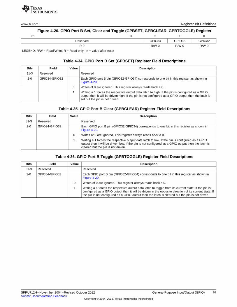
www.ti.com Register Bit Definitions
Figure 4-20. GPIO Port B Set, Clear and Toggle (GPBSET, GPBCLEAR, GPBTOGGLE) Register31 3 2 1 0
Reserved GPIO34 GPIO33 GPIO32
R-0 R/W-0 R/W-0 R/W-0
LEGEND: R/W = Read/Write; R = Read only; -n = value after reset
Table 4-34. GPIO Port B Set (GPBSET) Register Field Descriptions
Bits Field Value Description
31-3 Reserved Reserved
2-0 GPIO34-GPIO32 Each GPIO port B pin (GPIO32-GPIO34) corresponds to one bit in this register as shown inFigure 4-20.
0 Writes of 0 are ignored. This register always reads back a 0.
1 Writing a 1 forces the respective output data latch to high. If the pin is configured as a GPIOoutput then it will be driven high. If the pin is not configured as a GPIO output then the latch isset but the pin is not driven.
Table 4-35. GPIO Port B Clear (GPBCLEAR) Register Field Descriptions
Bits Field Value Description
31-3 Reserved Reserved
2-0 GPIO34-GPIO32 Each GPIO port B pin (GPIO32-GPIO34) corresponds to one bit in this register as shown inFigure 4-20.
0 Writes of 0 are ignored. This register always reads back a 0.
1 Writing a 1 forces the respective output data latch to low. If the pin is configured as a GPIOoutput then it will be driven low. If the pin is not configured as a GPIO output then the latch iscleared but the pin is not driven.
Table 4-36. GPIO Port B Toggle (GPBTOGGLE) Register Field Descriptions
Bits Field Value Description
31-3 Reserved Reserved
2-0 GPIO34-GPIO32 Each GPIO port B pin (GPIO32-GPIO34) corresponds to one bit in this register as shown inFigure 4-20.
0 Writes of 0 are ignored. This register always reads back a 0.
1 Writing a 1 forces the respective output data latch to toggle from its current state. If the pin isconfigured as a GPIO output then it will be driven in the opposite direction of its current state. Ifthe pin is not configured as a GPIO output then the latch is cleared but the pin is not driven.
99SPRU712H–November 2004–Revised October 2012 General-Purpose Input/Output (GPIO)Submit Documentation Feedback
Copyright © 2004–2012, Texas Instruments Incorporated

Register Bit Definitions www.ti.com
Figure 4-21. GPIO XINT1, XINT2, XNMI Interrupt Select (GPIOXINT1SEL, GPIOXINT2SEL,GPIOXNMISEL) Registers
15 5 4 0
Reserved GPIOSEL
R-0 R/W-0
LEGEND: R/W = Read/Write; R = Read only; -n = value after reset
Table 4-37. GPIO XINT1 Interrupt Select (GPIOXINT1SEL) Register Field Descriptions
Bits Field Value Description (1)
15-5 Reserved Reserved
4-0 GPIOSEL Select which port A GPIO signal (GPIO0 - GPIO31) will be used as the XINT1 interruptsource. In addition you can configure the interrupt in the XINT1CR register described inSection 6.6.
00000 Select the GPIO0 pin as the XINT1 interrupt source (default)
00001 Select the GPIO1 pin as the XINT1 interrupt source
. . . . . .
11110 Select the GPIO30 pin as the XINT1 interrupt source
11111 Select the GPIO31 pin as the XINT1 interrupt source(1) This register is EALLOW protected. See Section 5.2 for more information.
Table 4-38. GPIO XINT2 Interrupt Select (GPIOXINT2SEL) Register Field Descriptions
Bits Field Value Description (1)
15-5 Reserved Reserved
4-0 GPIOSEL Select which port A GPIO signal (GPIO0 - GPIO31) will be used as the XINT2 interrupt source.In addition you can configure the interrupt in the XINT2CR register described in Section 6.6.
To use the signal as ADC start of conversion, enable it in the ADCTRL2 register. The ADCSOCis always rising edge sensitive.
00000 Select the GPIO0 pin as the XINT2 interrupt source (default)
00001 Select the GPIO1 pin as the XINT2 interrupt source
. . . . . .
11110 Select the GPIO30 pin as the XINT2 interrupt source
11111 Select the GPIO31 pin as the XINT2 interrupt source(1) This register is EALLOW protected. See Section 5.2 for more information.
Table 4-39. GPIO XNMI Interrupt Select (GPIOXNMISEL) Register Field Descriptions
Bits Field Value Description (1)
15-5 Reserved Reserved
4-0 GPIOSEL Select which port A GPIO signal (GPIO0 - GPIO31) will be used as the XNMI interrupt source. Inaddition you can configure the interrupt in the XNMICR register described in Section 6.6.
00000 Select the GPIO0 pin as the XNMI interrupt source (default)
00001 Select the GPIO1 pin as the XNMI interrupt source
. . . . . .
11110 Select the GPIO30 pin as the XNMI interrupt source
11111 Select the GPIO31 pin as the XNMI interrupt source(1) This register is EALLOW protected. See Section 5.2 for more information.
100 General-Purpose Input/Output (GPIO) SPRU712H–November 2004–Revised October 2012Submit Documentation Feedback
Copyright © 2004–2012, Texas Instruments Incorporated

www.ti.com Register Bit Definitions
Figure 4-22. GPIO Low Power Mode Wakeup Select (GPIOLPMSEL) Register31 30 29 28 27 26 25 24
GPIO31 GPIO30 GPIO29 GPIO28 GPIO27 GPIO26 GPIO25 GPIO24
R/W-0 R/W-0 R/W-0 R/W-0 R/W-0 R/W-0 R/W-0 R/W-0
23 22 21 20 19 18 17 16
GPIO23 GPIO22 GPIO21 GPIO20 GPIO19 GPIO18 GPIO17 GPIO16
R/W-0 R/W-0 R/W-0 R/W-0 R/W-0 R/W-0 R/W-0 R/W-0
15 14 13 12 11 10 9 8
GPIO15 GPIO14 GPIO13 GPIO12 GPIO11 GPIO10 GPIO9 GPIO8
R/W-0 R/W-0 R/W-0 R/W-0 R/W-0 R/W-0 R/W-0 R/W-0
7 6 5 4 3 2 1 0
GPIO7 GPIO6 GPIO5 GPIO4 GPIO3 GPIO2 GPIO1 GPIO0
R/W-0 R/W-0 R/W-0 R/W-0 R/W-0 R/W-0 R/W-0 R/W-0
LEGEND: R/W = Read/Write; R = Read only; -n = value after reset
Table 4-40. GPIO Low Power Mode Wakeup Select (GPIOLPMSEL) Register Field Descriptions
Bits Field Value Description (1)
31-0 GPIO31 - GPIO0 Low Power Mode Wakeup Selection. Each bit in this register corresponds to one GPIO portA pin (GPIO0 - GPIO31) as shown in Figure 4-22.
0 If the bit is cleared, the signal on the corresponding pin will have no effect on the HALT andSTANDBY low power modes.
1 If the respective bit is set to 1, the signal on the corresponding pin is able to wake thedevice from both HALT and STANDBY low power modes.
(1) This register is EALLOW protected. See Section 5.2 for more information.
Figure 4-23. GPIOA Miscellaneous Configuration Register (GPAMCFG) (28044 only)31 2 1 0
Spares EPWMMODE
R-0 R/W-00
LEGEND: R/W = Read/Write; R = Read only; -n = value after reset
Table 4-41. GPIOA Miscellaneous Configuration Register (GPAMCFG) Field Descriptions (28044only)
Bit Field Value Description (1)
31:2 Spare 00 Reserved
1:0 EPWMMODE The ePWM Mode (28044 device only)Configure the pinout of the ePWM output and TZn input signals for GPIO0-GPIO15. This selectionis only used when the corresponding GPAMUX1 bits are set to peripheral selection 1 (that is, 0,1).See Table 4-13.
00 TMS320x280x compatible mode (default on reset)EPWM1 to EPWM6 (channels A and B) are brought out on GPIO0 to GPIO11 and TZ1, TZ2, TZ3,and TZ4 are brought out on GPIO12 to GPIO15.
01 Reserved, do not use
10 Reserved, do not use
11 EPWMxA channel only mode:EPWM1A to EPWM16A are brought out sequentially on GPIO0 to GPIO15. EPWMxB outputsignals are not available in this mode.
(1) This register is EALLOW protected.
101SPRU712H–November 2004–Revised October 2012 General-Purpose Input/Output (GPIO)Submit Documentation Feedback
Copyright © 2004–2012, Texas Instruments Incorporated

Chapter 5SPRU712H–November 2004–Revised October 2012
Peripheral Frames
This chapter describes the peripheral frames. It also describes the device emulation registers.
Topic ........................................................................................................................... Page
5.1 Peripheral Frame Registers ............................................................................... 1035.2 EALLOW-Protected Registers ........................................................................... 1045.3 Device Emulation Registers .............................................................................. 1095.4 Write-Followed-by-Read Protection .................................................................... 110
102 Peripheral Frames SPRU712H–November 2004–Revised October 2012Submit Documentation Feedback
Copyright © 2004–2012, Texas Instruments Incorporated

www.ti.com Peripheral Frame Registers
5.1 Peripheral Frame Registers
The 280x devices contain three peripheral register spaces. The spaces are categorized as follows:
• Peripheral Frame 0: These are peripherals that are mapped directly to the CPU memory bus. SeeTable 5-1.
• Peripheral Frame 1: These are peripherals that are mapped to the 32-bit peripheral bus. See Table 5-2.
• Peripheral Frame 2: These are peripherals that are mapped to the 16-bit peripheral bus. See Table 5-3.
Table 5-1. Peripheral Frame 0 Registers
Name Address Range Size (x16) Access Type (1)
Device Emulation Registers 0x0880 - 0x09FF 384 EALLOW-protected
FLASH Registers (2) 0x0A80 - 0x0ADF 96 EALLOW-protected. CSM Protected
Code Security Module Registers 0x0AE0 - 0x0AEF 16 EALLOW-protected
CPU-TIMER0/1/2 Registers 0x0C00 - 0x0C3F 64 Not EALLOW-protected
PIE Registers 0x0CE0 - 0x0CFF 32 Not EALLOW-protected
PIE Vector Table 0x0D00 - 0x0DFF 256 EALLOW-protected(1) If registers are EALLOW-protected, you cannot perform writes until you execute the EALLOW instruction. The EDIS instruction
disables writes to prevent stray code or pointers from corrupting register contents.(2) The flash registers are also protected by the Code Security Module (CSM).
Table 5-2. Peripheral Frame 1 Registers
Name Address Range Size (x16) Access Type (1)
eCANA Registers 0x6000 - 0x60FF 256 Some eCAN control registers (and selected bits inother eCAN control registers) are EALLOW-protected.
eCANA Mailbox RAM 0x6100 - 0x61FF 256 Not EALLOW-protected
eCANB Registers 0x6200 - 0x62FF 256 Some eCAN control registers (and selected bits inother eCAN control registers) are EALLOW-protected.
eCANB Mailbox RAM 0x6300 - 0x63FF 256 Not EALLOW-protected
ePWM1 Registers 0x6800 - 0x683F 64) Some ePWM registers are EALLOW-protected. SeeSection 5.2.ePWM2 Registers 0x6840 - 0x687F 64
ePWM3 Registers 0x6880 - 0x68BF 64
ePWM4 Registers 0x68C0 - 0x68FF 64
ePWM5 Registers 0x6900 - 0x693F 64
ePWM6 Registers 0x6940 - 0x697F 64
ePWM7 Registers 0x6980 - 0x69BF 64 Some ePWM registers are EALLOW-protected. SeeSection 5.2. The ePWM7 through ePWM16ePWM8 Registers 0x69C0 - 0x69FF 64registers are applicable to 28044 device only.
ePWM9 Registers 0x6600 - 0x663F 64
ePWM10 Registers 0x6640 - 0x667F 64
ePWM11 Registers 0x6680 - 0x66BF 64
ePWM12 Registers 0x66C0 - 0x66FF 64
ePWM13 Registers 0x6700 - 0x673F 64
ePWM14 Registers 0x6740 - 0x677F 64
ePWM15 Registers 0x6780 - 0x67BF 64
ePWM16 Registers 0x6980 - 0x69FF 64
eCAP1 Registers 0x6A00 - 0x6A1F 32 Not EALLOW-protected
eCAP2 Registers 0x6A20 - 0x6A3F 32 Not EALLOW-protected
eCAP3 Registers 0x6A40 - 0x6A5F 32 Not EALLOW-protected
(1) Peripheral Frame 1 allows 16-bit and 32-bit accesses. All 32-bit accesses are aligned to even address boundaries.
103SPRU712H–November 2004–Revised October 2012 Peripheral FramesSubmit Documentation Feedback
Copyright © 2004–2012, Texas Instruments Incorporated

EALLOW-Protected Registers www.ti.com
Table 5-2. Peripheral Frame 1 Registers (continued)
Name Address Range Size (x16) Access Type (1)
eCAP4 Registers 0x6A60 - 0x6A7F 32 Not EALLOW-protected
Reserved 0x6A80 - 0x6AFF 32 Not EALLOW-protected
eQEP1 Registers 0x6B00 - 0x6B3F 64 Not EALLOW-protected
eQEP2 Registers 0x6B40 - 0x6B7F 64 Not EALLOW-protected
GPIO Control Registers 0x6F80 - 0x6FBF 128 EALLOW-protected
GPIO Data Registers 0x6FC0 - 0x6FDF 32 Not EALLOW-protected
GPIO Interrupt and LPM Select 0x6FE0 - 0x6FFF 32 EALLOW-protectedRegisters
Table 5-3. Peripheral Frame 2 Registers
Name Address Range Size (x16) Access Type (1)
System Control Registers 0x7010 - 0x702F 32 EALLOW-protected
SPI-A Registers 0x7040 - 0x704F 16 Not EALLOW-protected
SCI-A Registers 0x7050 - 0x705F 16 Not EALLOW-protected
ADC Registers 0x7100 - 0x711F 32 Not EALLOW-protected
SPI-B Registers 0x7740 - 0x774F 16 Not EALLOW-protected
SCI-B Registers 0x7750 - 0x775F 16 Not EALLOW-protected
SPI-C Registers 0x7760 - 0x776F 16 Not EALLOW-protected
SPI-D Registers 0x7780 - 0x778F 16 Not EALLOW-protected
I2C Registers 0x7900 - 0x793F 64 Not EALLOW-protected(1) Peripheral Frame 2 only allows 16-bit accesses. All 32-bit accesses are ignored (invalid data can be returned or written).
5.2 EALLOW-Protected Registers
Several control registers on the 280x devices are protected from spurious CPU writes by the EALLOWprotection mechanism. The EALLOW bit in status register 1 (ST1) indicates if the state of protection asshown in Table 5-4.
Table 5-4. Access to EALLOW-Protected Registers
EALLOW Bit CPU Writes CPU Reads JTAG Writes JTAG Reads
0 Ignored Allowed Allowed (1) Allowed
1 Allowed Allowed Allowed Allowed(1) The EALLOW bit is overridden via the JTAG port, allowing full access of protected registers during debug from the Code
Composer Studio interface.
At reset the EALLOW bit is cleared enabling EALLOW protection. While protected, all writes to protectedregisters by the CPU are ignored and only CPU reads, JTAG reads, and JTAG writes are allowed. If thisbit is set, by executing the EALLOW instruction, then the CPU is allowed to write freely to protectedregisters. After modifying registers, they can once again be protected by executing the EDI instruction toclear the EALLOW bit.
The following registers are EALLOW-protected:
• Device Emulation Registers
• Flash Registers
• CSM Registers
• PIE Vector Table
• System Control Registers
• GPIO MUX Registers
• Certain eCAN Registers
104 Peripheral Frames SPRU712H–November 2004–Revised October 2012Submit Documentation Feedback
Copyright © 2004–2012, Texas Instruments Incorporated

www.ti.com EALLOW-Protected Registers
Table 5-5. EALLOW-Protected Device Emulation Registers
Name Address Size Description(x16)
DEVICECNF 0x0880 2 Device Configuration Register0x0881
PROTSTART 0x0884 1 Block Protection Start Address Register
PROTRANGE 0x0885 1 Block Protection Range Address Register
Table 5-6. EALLOW-Protected Flash/OTP Configuration Registers
SizeName Address (x16) Description
FOPT 0x0A80 1 Flash Option Register
FPWR 0x0A82 1 Flash Power Modes Register
FSTATUS 0x0A83 1 Status Register
FSTDBYWAIT 0x0A84 1 Flash Sleep To Standby Wait State Register
FACTIVEWAIT 0x0A85 1 Flash Standby To Active Wait State Register
FBANKWAIT 0x0A86 1 Flash Read Access Wait State Register
FOTPWAIT 0x0A87 1 OTP Read Access Wait State Register
Table 5-7. EALLOW-Protected Code Security Module (CSM) Registers
SizeRegister Name Address Register Description(x16)
KEY0 0x0AE0 1 Low word of the 128-bit KEY register
KEY1 0x0AE1 1 Second word of the 128-bit KEY register
KEY2 0x0AE2 1 Third word of the 128-bit KEY register
KEY3 0x0AE3 1 Fourth word of the 128-bit KEY register
KEY4 0x0AE4 1 Fifth word of the 128-bit KEY register
KEY5 0x0AE5 1 Sixth word of the 128-bit KEY register
KEY6 0x0AE6 1 Seventh word of the 128-bit KEY register
KEY7 0x0AE7 1 High word of the 128-bit KEY register
CSMSCR 0x0AEF 1 CSM status and control register
Table 5-8. EALLOW-Protected PIE Vector Table
SizeName Address (x16) Description
Not used 0x0D00 2 Reserved
0x0D02
0x0D04
0x0D06
0x0D08
0x0D0A
0x0D0C
0x0D0E
0x0D10
0x0D12
0x0D14
0x0D16
0x0D18
105SPRU712H–November 2004–Revised October 2012 Peripheral FramesSubmit Documentation Feedback
Copyright © 2004–2012, Texas Instruments Incorporated
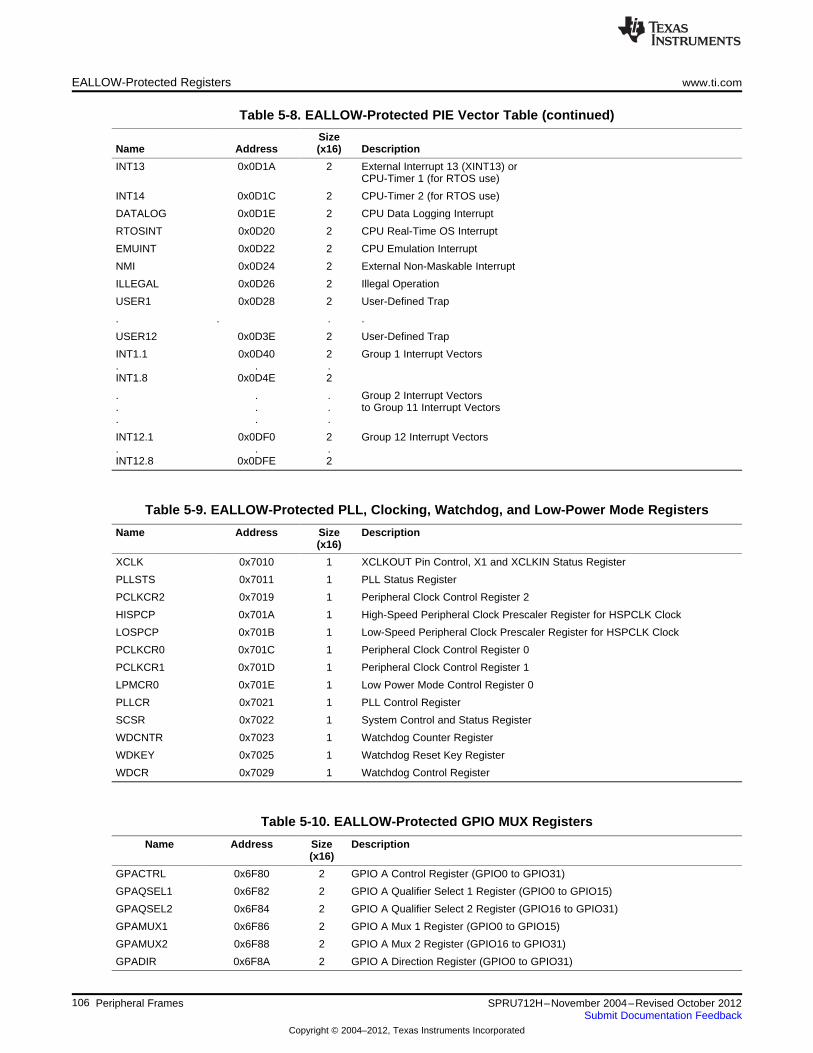
EALLOW-Protected Registers www.ti.com
Table 5-8. EALLOW-Protected PIE Vector Table (continued)
SizeName Address (x16) Description
INT13 0x0D1A 2 External Interrupt 13 (XINT13) orCPU-Timer 1 (for RTOS use)
INT14 0x0D1C 2 CPU-Timer 2 (for RTOS use)
DATALOG 0x0D1E 2 CPU Data Logging Interrupt
RTOSINT 0x0D20 2 CPU Real-Time OS Interrupt
EMUINT 0x0D22 2 CPU Emulation Interrupt
NMI 0x0D24 2 External Non-Maskable Interrupt
ILLEGAL 0x0D26 2 Illegal Operation
USER1 0x0D28 2 User-Defined Trap
. . . .
USER12 0x0D3E 2 User-Defined Trap
INT1.1 0x0D40 2 Group 1 Interrupt Vectors. . .INT1.8 0x0D4E 2
. . . Group 2 Interrupt Vectors
. . . to Group 11 Interrupt Vectors
. . .
INT12.1 0x0DF0 2 Group 12 Interrupt Vectors. . .INT12.8 0x0DFE 2
Table 5-9. EALLOW-Protected PLL, Clocking, Watchdog, and Low-Power Mode Registers
Name Address Size Description(x16)
XCLK 0x7010 1 XCLKOUT Pin Control, X1 and XCLKIN Status Register
PLLSTS 0x7011 1 PLL Status Register
PCLKCR2 0x7019 1 Peripheral Clock Control Register 2
HISPCP 0x701A 1 High-Speed Peripheral Clock Prescaler Register for HSPCLK Clock
LOSPCP 0x701B 1 Low-Speed Peripheral Clock Prescaler Register for HSPCLK Clock
PCLKCR0 0x701C 1 Peripheral Clock Control Register 0
PCLKCR1 0x701D 1 Peripheral Clock Control Register 1
LPMCR0 0x701E 1 Low Power Mode Control Register 0
PLLCR 0x7021 1 PLL Control Register
SCSR 0x7022 1 System Control and Status Register
WDCNTR 0x7023 1 Watchdog Counter Register
WDKEY 0x7025 1 Watchdog Reset Key Register
WDCR 0x7029 1 Watchdog Control Register
Table 5-10. EALLOW-Protected GPIO MUX Registers
Name Address Size Description(x16)
GPACTRL 0x6F80 2 GPIO A Control Register (GPIO0 to GPIO31)
GPAQSEL1 0x6F82 2 GPIO A Qualifier Select 1 Register (GPIO0 to GPIO15)
GPAQSEL2 0x6F84 2 GPIO A Qualifier Select 2 Register (GPIO16 to GPIO31)
GPAMUX1 0x6F86 2 GPIO A Mux 1 Register (GPIO0 to GPIO15)
GPAMUX2 0x6F88 2 GPIO A Mux 2 Register (GPIO16 to GPIO31)
GPADIR 0x6F8A 2 GPIO A Direction Register (GPIO0 to GPIO31)
106 Peripheral Frames SPRU712H–November 2004–Revised October 2012Submit Documentation Feedback
Copyright © 2004–2012, Texas Instruments Incorporated

www.ti.com EALLOW-Protected Registers
Table 5-10. EALLOW-Protected GPIO MUX Registers (continued)
Name Address Size Description(x16)
GPAPUD 0x6F8C 2 GPIO A Pull Up Disable Register (GPIO0 to GPIO31)
GPAMCFG 0x6F8E 2 GPIO A Miscellaneous Configuration Register (GPIO0 to 31)
GPBCTRL 0x6F90 2 GPIO B Control Register (GPIO32 to GPIO35)
GPBQSEL1 0x6F92 2 GPIO B Qualifier Select 1 Register (GPIO32 to GPIO35)
GPBQSEL2 0x6F94 2 Reserved
GPBMUX1 0x6F96 2 GPIO B Mux 1 Register (GPIO32 to GPIO35)
GPBMUX2 0x6F98 2 reserved
GPBDIR 0x6F9A 2 GPIO B Direction Register (GPIO32 to GPIO35)
GPBPUD 0x6F9C 2 GPIO B Pull Up Disable Register (GPIO32 to GPIO35)
GPIOXINT1SEL 0x6FE0 1 XINT1 GPIO Input Select Register (GPIO0 to GPIO31)
GPIOXINT2SEL 0x6FE1 1 XINT2 GPIO Input Select Register (GPIO0 to GPIO31)
GPIOXNMISEL 0x6FE2 1 XNMI GPIO Input Select Register (GPIO0 to GPIO31)
GPIOLPMSEL 0x6FE8 2 LPM GPIO Select Register (GPIO0 to GPIO31)
Table 5-11. EALLOW-Protected eCAN-A Registers
Name eCAN-A eCAN-B Size (x16) DescriptionAddress Address
CANMC 0x6014 0x6214 2 Master Control Register (1)
CANBTC 0x6016 0x6216 2 Bit Timing Configuration Register (2)
CANGIM 0x6020 0x6220 2 Global Interrupt Mask Register (3)
CANMIM 0x6024 0x6224 2 Mailbox Interrupt Mask Register
CANTSC 0x602E 0x622E 2 Time Stamp Counter
CANTIOC 0x602A 0x622A 1 I/O Control Register for CANTXA Pin (4)
CANRIOC 0x602C 0x622C 1 I/O Control Register for CANRXA Pin (5)
(1) Only bits CANMC[15-9] and [7-6] are protected(2) Only bits BCR[23-16] and [10-0] are protected(3) Only bits CANGIM[17-16] , [14-8], and [2-0] are protected(4) Only IOCONT1[3] is protected(5) Only IOCONT2[3] is protected
Table 5-12 shows addresses for the following ePWM EALLOW-protected registers:
• Trip Zone Select Register (TZSEL)
• Trip Zone Control Register (TZCTL)
• Trip Zone Enable Interrupt Register (TZEINT)
• Trip Zone Clear Register (TZCLR)
• Trip Zone Force Register (TZFRC)
• HRPWM Configuration Register (HRCNFG)
Table 5-12. EALLOW-Protected ePWM1 - ePWM16 Registers
TZSEL TZCTL TZEINT TZCLR TZFRC HRCNFG Size x16
ePWM1 0x6812 0x6814 0x6815 0x6817 0x6818 0x6820 1
ePWM2 0x6852 0x6854 0x6855 0x6857 0x6858 0x6860 1
ePWM3 0x6892 0x6894 0x6895 0x6897 0x6898 0x68A0 1
ePWM4 0x68D2 0x68D4 0x68D5 0x68D7 0x68D8 0x68E0 1
ePWM5 0x6912 0x6914 0x6915 0x6917 0x6918 0x6920 1
ePWM6 0x6952 0x6954 0x6955 0x6957 0x6958 0x6960 1
107SPRU712H–November 2004–Revised October 2012 Peripheral FramesSubmit Documentation Feedback
Copyright © 2004–2012, Texas Instruments Incorporated

EALLOW-Protected Registers www.ti.com
Table 5-12. EALLOW-Protected ePWM1 - ePWM16 Registers (continued)
TZSEL TZCTL TZEINT TZCLR TZFRC HRCNFG Size x16
ePWM7 0x6992 0x6994 0x6995 0x6997 0x6998 0x69A0 1
ePWM8 0x69D2 0x69D4 0x69D5 0x69D7 0x69D8 0x69E0 1
ePWM9 0x6612 0x6614 0x6615 0x6617 0x6618 0x6620 1
ePWM10 0x6652 0x6654 0x6655 0x6657 0x6658 0x6660 1
ePWM11 0x6692 0x6694 0x6695 0x6697 0x6698 0x66A0 1
ePWM12 0x66D2 0x66D4 0x66D5 0x66D7 0x66D8 0x66E0 1
ePWM13 0x6712 0x6714 0x6715 0x6717 0x6718 0x6720 1
ePWM14 0x6752 0x6754 0x6755 0x6757 0x6758 0x6760 1
ePWM15 0x6792 0x6794 0x6795 0x6797 0x6798 0x67A0 1
ePWM16 0x67D2 0x67D4 0x67D5 0x67D7 0x67D8 0x67E0 1
108 Peripheral Frames SPRU712H–November 2004–Revised October 2012Submit Documentation Feedback
Copyright © 2004–2012, Texas Instruments Incorporated
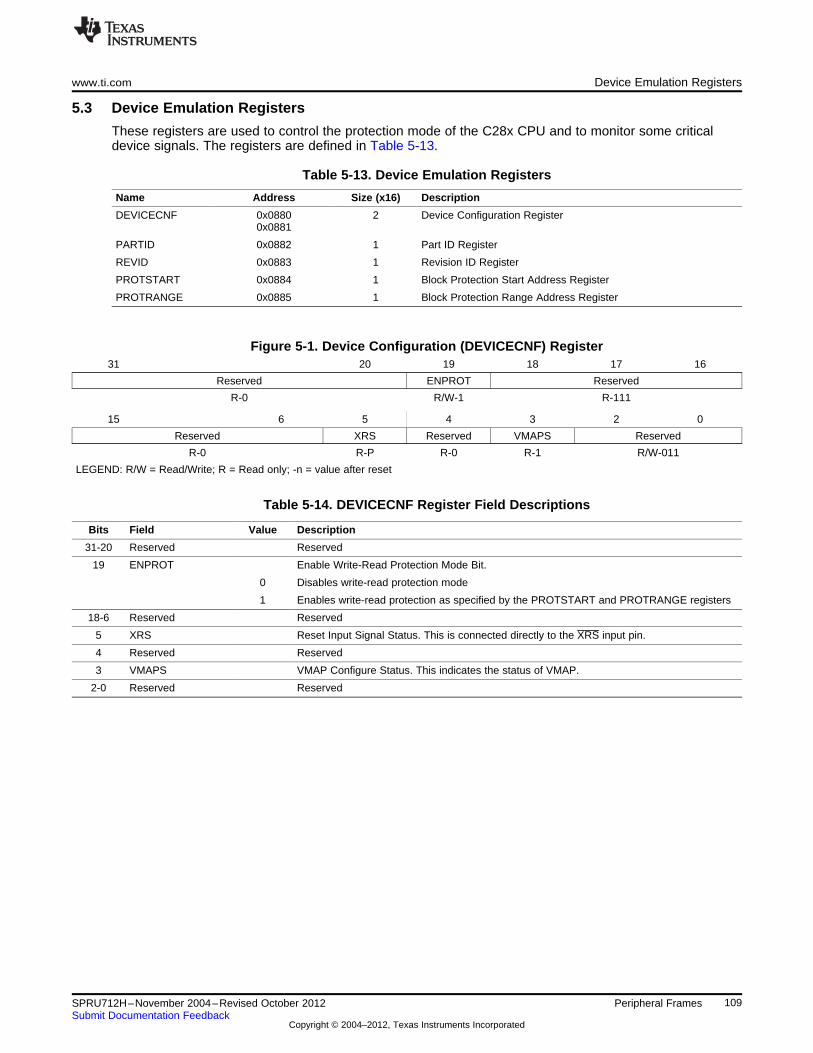
www.ti.com Device Emulation Registers
5.3 Device Emulation Registers
These registers are used to control the protection mode of the C28x CPU and to monitor some criticaldevice signals. The registers are defined in Table 5-13.
Table 5-13. Device Emulation Registers
Name Address Size (x16) Description
DEVICECNF 0x0880 2 Device Configuration Register0x0881
PARTID 0x0882 1 Part ID Register
REVID 0x0883 1 Revision ID Register
PROTSTART 0x0884 1 Block Protection Start Address Register
PROTRANGE 0x0885 1 Block Protection Range Address Register
Figure 5-1. Device Configuration (DEVICECNF) Register31 20 19 18 17 16
Reserved ENPROT Reserved
R-0 R/W-1 R-111
15 6 5 4 3 2 0
Reserved XRS Reserved VMAPS Reserved
R-0 R-P R-0 R-1 R/W-011
LEGEND: R/W = Read/Write; R = Read only; -n = value after reset
Table 5-14. DEVICECNF Register Field Descriptions
Bits Field Value Description
31-20 Reserved Reserved
19 ENPROT Enable Write-Read Protection Mode Bit.
0 Disables write-read protection mode
1 Enables write-read protection as specified by the PROTSTART and PROTRANGE registers
18-6 Reserved Reserved
5 XRS Reset Input Signal Status. This is connected directly to the XRS input pin.
4 Reserved Reserved
3 VMAPS VMAP Configure Status. This indicates the status of VMAP.
2-0 Reserved Reserved
109SPRU712H–November 2004–Revised October 2012 Peripheral FramesSubmit Documentation Feedback
Copyright © 2004–2012, Texas Instruments Incorporated

Write-Followed-by-Read Protection www.ti.com
Figure 5-2. Part ID Register15 8 7 0
PARTTYPE PARTNO
R R
LEGEND: R/W = Read/Write; R = Read only; -n = value after reset
Table 5-15. PARTID Register Field Descriptions
Bits Field Type Reset Value Description
7-0 PARTNO R (1) These 8 bits specify the feature set of the device as follows:
0xFE 2809
0x2C 2801/9501
0x34 2806
0x3C 2808
0x14 F28016
0x1C F28015
0x2C C2801
0x24 C2802
All other values are reserved or used by other devices.
15-8 PARTTYPE R (1) These 8 bits specify the type of device such as flash-based or ROM-based.
0x00 Flash-based device
0xFF ROM-based device
All other values are reserved.(1) The reset value depends on the device as indicated in the register description.
Figure 5-3. REVID Register15 0
REVID
R
LEGEND: R/W = Read/Write; R = Read only; -n = value after reset
Table 5-16. REVID Register Field Descriptions
Bits Field Reset Description
15-0 REVID (1)These 16 bits specify the silicon revision number for the particular part. This numberalways starts with 0x0000 on the first revision of the silicon and is incremented on anysubsequent revisions.
0x0000 Revision 0 (for first silicon)
0x0001 Revision A
0x0002 Revision B and so forth(1) The reset value depends on the silicon revision as described in the register field description.
5.4 Write-Followed-by-Read Protection
The PROTSTART and PROTRANGE registers set the memory address range for which CPU "write"followed by "read" operations are protected (operations occur in sequence rather then in their naturalpipeline order). This is necessary protection for certain peripheral operations.
Example: The following lines of code perform a write to register 1 (REG1) location and then the nextinstruction performs a read from Register 2 (REG2) location. On the processor memory bus, with blockprotection disabled, the read operation is issued before the write as shown.MOV @REG1,AL ---------+ TBIT @REG2,#BIT_X ---------|-------> Read +-------> Write
110 Peripheral Frames SPRU712H–November 2004–Revised October 2012Submit Documentation Feedback
Copyright © 2004–2012, Texas Instruments Incorporated

www.ti.com Write-Followed-by-Read Protection
If block protection is enabled, then the read is stalled until the write occurs as shown:MOV @REG1,AL ---------+ TBIT @REG2,#BIT_X ---------|-----+ +-----|---> Write +---> Read
Table 5-17. PROTSTART and PROTRANGE Registers
Name Address Size Type Reset Description
PROTSTART 0x0884 16 R/W 0x0100 (1) The PROTSTART register sets the starting addressrelative to the 16 most significant bits of theprocessors lower 22-bit address reach. Hence, thesmallest resolution is 64 words.
PROTRANGE 0x0885 16 R/W 0x00FF (1) The PROTRANGE register sets the block size (fromthe starting address), starting with 64 words andincrementing by binary multiples (64, 128, 256, 512,1K, 2K, 4K, 8K, 16K, ...., 2M).
(1) The default values of these registers on reset are selected to cover the Peripheral Frame 1, Peripheral Frame 2, and XINTFZone 1 areas of the memory map (address range 0x4000 to 0x8000).
Table 5-18. PROTSTART Valid Values
Register Bits (1)
Start Address Register Value 15 14 13 12 11 10 9 8 7 6 5 4 3 2 1 0
0x0000 0000 0x0000 0 0 0 0 0 0 0 0 0 0 0 0 0 0 0 0
0x0000 0040 0x0001 0 0 0 0 0 0 0 0 0 0 0 0 0 0 0 1
0x0000 0080 0x0002 0 0 0 0 0 0 0 0 0 0 0 0 0 0 1 0
0x0000 00C0 0x0003 0 0 0 0 0 0 0 0 0 0 0 0 0 0 1 1
. . . . . . . . . . . . . . . . . .
. . . . . . . . . . . . . . . . . .
0x003F FF00 0xFFFC 1 1 1 1 1 1 1 1 1 1 1 1 1 1 0 0
0x003F FF40 0xFFFD 1 1 1 1 1 1 1 1 1 1 1 1 1 1 0 1
0x003F FF80 0xFFFE 1 1 1 1 1 1 1 1 1 1 1 1 1 1 1 0
0x003F FFC0 0xFFFF 1 1 1 1 1 1 1 1 1 1 1 1 1 1 1 1(1) The quickest way to calculate register value is to divide the desired block starting address by 64.
Table 5-19. PROTRANGE Valid Values
Register Bits (1)
Block Size Register Value 15 14 13 12 11 10 9 8 7 6 5 4 3 2 1 0
64 0x0000 0 0 0 0 0 0 0 0 0 0 0 0 0 0 0 0
128 0x0001 0 0 0 0 0 0 0 0 0 0 0 0 0 0 0 1
256 0x0003 0 0 0 0 0 0 0 0 0 0 0 0 0 0 1 1
512 0x0007 0 0 0 0 0 0 0 0 0 0 0 0 0 1 1 1
1K 0x000F 0 0 0 0 0 0 0 0 0 0 0 0 1 1 1 1
. . . . . . . . . . . . . . . . . .
. . . . . . . . . . . . . . . . . .
256K 0x0FFF 0 0 0 0 1 1 1 1 1 1 1 1 1 1 1 1
512K 0x1FFF 0 0 0 1 1 1 1 1 1 1 1 1 1 1 1 1
1M 0x3FFF 0 0 1 1 1 1 1 1 1 1 1 1 1 1 1 1
2M 0x7FFF 0 1 1 1 1 1 1 1 1 1 1 1 1 1 1 1
4M 0xFFFF 1 1 1 1 1 1 1 1 1 1 1 1 1 1 1 1(1) Not all register values are valid. The PROTSTART address value must be a multiple of the range value. For example: if the
block size is set to 4K, then the start address can only be at any 4K boundary.
111SPRU712H–November 2004–Revised October 2012 Peripheral FramesSubmit Documentation Feedback
Copyright © 2004–2012, Texas Instruments Incorporated

Chapter 6SPRU712H–November 2004–Revised October 2012
Peripheral Interrupt Expansion (PIE)
The peripheral interrupt expansion (PIE) block multiplexes numerous interrupt sources into a smaller set ofinterrupt inputs. The PIE block can support 96 individual interrupts that are grouped into blocks of eight.Each group is fed into one of 12 core interrupt lines (INT1 to INT12). Each of the 96 interrupts issupported by its own vector stored in a dedicated RAM block that you can modify. The CPU, uponservicing the interrupt, automatically fetches the appropriate interrupt vector. It takes nine CPU clockcycles to fetch the vector and save critical CPU registers. Therefore, the CPU can respond quickly tointerrupt events. Prioritization of interrupts is controlled in hardware and software. Each individual interruptcan be enabled/disabled within the PIE block.
Topic ........................................................................................................................... Page
6.1 Overview of the PIE Controller .......................................................................... 1136.2 Vector Table Mapping ...................................................................................... 1166.3 Interrupt Sources ............................................................................................. 1176.4 PIE Configuration Registers .............................................................................. 1336.5 PIE Interrupt Registers ..................................................................................... 1356.6 External Interrupt Control Registers ................................................................... 142
112 Peripheral Interrupt Expansion (PIE) SPRU712H–November 2004–Revised October 2012Submit Documentation Feedback
Copyright © 2004–2012, Texas Instruments Incorporated

INT12
MUX
INT11
INT2INT1
CPU
(Enable)(Flag)
INTx
INTx.8
PIEIERx(8:1) PIEIFRx(8:1)
MUX
INTx.7INTx.6
INTx.5INTx.4INTx.3INTx.2INTx.1
Fromperipherals or
externalinterrupts
(Enable) (Flag)
IER(12:1)IFR(12:1)
Globalenable
INTM
1
0
PIEACKx
(Enable/flag)
www.ti.com Overview of the PIE Controller
6.1 Overview of the PIE Controller
The 28x CPU supports one nonmaskable interrupt (NMI) and 16 maskable prioritized interrupt requests(INT1-INT14, RTOSINT, and DLOGINT) at the CPU level. The 28x devices have many peripherals andeach peripheral is capable of generating one or more interrupts in response to many events at theperipheral level. Because the CPU does not have sufficient capacity to handle all peripheral interruptrequests at the CPU level, a centralized peripheral interrupt expansion (PIE) controller is required toarbitrate the interrupt requests from various sources such as peripherals and other external pins.
The PIE vector table is used to store the address (vector) of each interrupt service routine (ISR) within thesystem. There is one vector per interrupt source including all MUXed and nonMUXed interrupts. Youpopulate the vector table during device initialization and you can update it during operation.
6.1.1 Interrupt Operation Sequence
Figure 6-1 shows an overview of the interrupt operation sequence for all multiplexed PIE interrupts.Interrupt sources that are not multiplexed are fed directly to the CPU.
Figure 6-1. Overview: Multiplexing of Interrupts Using the PIE Block
• Peripheral LevelAn interrupt-generating event occurs in a peripheral. The interrupt flag (IF) bit corresponding to thatevent is set in a register for that particular peripheral.
If the corresponding interrupt enable (IE) bit is set, the peripheral generates an interrupt request to thePIE controller. If the interrupt is not enabled at the peripheral level, then the IF remains set untilcleared by software. If the interrupt is enabled at a later time, and the interrupt flag is still set, theinterrupt request is asserted to the PIE.
Interrupt flags within the peripheral registers must be manually cleared. See the peripheral referenceguide for a specific peripheral for more information.
• PIE LevelThe PIE block multiplexes eight peripheral and external pin interrupts into one CPU interrupt. Theseinterrupts are divided into 12 groups: PIE group 1 - PIE group 12. The interrupts within a group aremultiplexed into one CPU interrupt. For example, PIE group 1 is multiplexed into CPU interrupt 1(INT1) while PIE group 12 is multiplexed into CPU interrupt 12 (INT12). Interrupt sources connected tothe remaining CPU interrupts are not multiplexed. For the nonmultiplexed interrupts, the PIE passesthe request directly to the CPU.
For multiplexed interrupt sources, each interrupt group in the PIE block has an associated flag register
113SPRU712H–November 2004–Revised October 2012 Peripheral Interrupt Expansion (PIE)Submit Documentation Feedback
Copyright © 2004–2012, Texas Instruments Incorporated

Overview of the PIE Controller www.ti.com
(PIEIFRx) and enable (PIEIERx) register (x = PIE group 1 - PIE group 12). Each bit, referred to as y,corresponds to one of the 8 MUXed interrupts within the group. Thus PIEIFRx.y and PIEIERx.ycorrespond to interrupt y (y = 1-8) in PIE group x (x = 1-12). In addition, there is one acknowledge bit(PIEACK) for every PIE interrupt group referred to as PIEACKx (x = 1-12). Figure 6-2 illustrates thebehavior of the PIE hardware under various PIEIFR and PIEIER register conditions.
Once the request is made to the PIE controller, the corresponding PIE interrupt flag (PIEIFRx.y) bit isset. If the PIE interrupt enable (PIEIERx.y) bit is also set for the given interrupt then the PIE checks thecorresponding PIEACKx bit to determine if the CPU is ready for an interrupt from that group. If thePIEACKx bit is clear for that group, then the PIE sends the interrupt request to the CPU. If PIEACKx isset, then the PIE waits until it is cleared to send the request for INTx. See Section 6.3 for details.
• CPU LevelOnce the request is sent to the CPU, the CPU level interrupt flag (IFR) bit corresponding to INTx is set.After a flag has been latched in the IFR, the corresponding interrupt is not serviced until it isappropriately enabled in the CPU interrupt enable (IER) register or the debug interrupt enable register(DBGIER) and the global interrupt mask (INTM) bit.
114 Peripheral Interrupt Expansion (PIE) SPRU712H–November 2004–Revised October 2012Submit Documentation Feedback
Copyright © 2004–2012, Texas Instruments Incorporated

Start
Stage APIEIFRx.y=1
?
Wait for anyPIEIFRx.y=1
No
Wait forPIEIERx.y=1
Stage BPIEIERx.y=1
?
No
PIEACKx=0Stage C
?
NoWait forS/W to clear
PIEACKx bit=0
Yes
Yes
Yes
Hardware setsPIEACKx=1
Stage DInterrupt requestsent to 28x CPU
on INTx
Interruptsto CPU
Stage EIFRx bit set 1
Yes
Stage GINTM bit=0
?
No
Yes
IERx bit=1Stage F
?
No
Stage HCPU responds
IFRx=0, IERx=0INTM=1, EALLOW=0
Context Save performed
Stage IVector fetched from the PIE(A)
PIEIFRx.y is clearedCPU branches to ISR
Stage JInterrupt service routine responds
Write 1 to PIEACKx bit to clearto enable other interrupts in
PIEIFRx groupRe-enable interrupts, INTM=0
Return
End
CPU interrupt controlPIE interrupt control
www.ti.com Overview of the PIE Controller
Figure 6-2. Typical PIE/CPU Interrupt Response - INTx.y
A Note: For multiplexed interrupts, the PIE responds with the highest priority interrupt that is both flagged and enabled.If there is no interrupt both flagged and enabled, then the highest priority interrupt within the group (INTx.1 where x isthe PIE group) is used. See Section Section 6.3.3 for details.
As shown in Table 6-1, the requirements for enabling the maskable interrupt at the CPU level depends onthe interrupt handling process being used. In the standard process, which happens most of the time, theDBGIER register is not used. When the 28x is in real-time emulation mode and the CPU is halted, adifferent process is used. In this special case, the DBGIER is used and the INTM bit is ignored. If the DSPis in real-time mode and the CPU is running, the standard interrupt-handling process applies.
Table 6-1. Enabling Interrupt
Interrupt Handling Process Interrupt Enabled If…
Standard INTM = 0 and bit in IER is 1
DSP in real-time mode and halted Bit in IER is 1 and DBGIER is 1
115SPRU712H–November 2004–Revised October 2012 Peripheral Interrupt Expansion (PIE)Submit Documentation Feedback
Copyright © 2004–2012, Texas Instruments Incorporated

Vector Table Mapping www.ti.com
The CPU then prepares to service the interrupt. This preparation process is described in detail inTMS320C28x DSP CPU and Instruction Set Reference Guide (literature number SPRU430). Inpreparation, the corresponding CPU IFR and IER bits are cleared, EALLOW and LOOP are cleared, INTMand DBGM are set, the pipeline is flushed and the return address is stored, and the automatic contextsave is performed. The vector of the ISR is then fetched from the PIE module. If the interrupt requestcomes from a multiplexed interrupt, the PIE module uses the group PIEIERx and PIEIFRx registers todecode which interrupt needs to be serviced. This decode process is described in detail in SectionSection 6.3.3.
The address for the interrupt service routine that is executed is fetched directly from the PIE interruptvector table. There is one 32-bit vector for each of the possible 96 interrupts within the PIE. Interrupt flagswithin the PIE module (PIEIFRx.y) are automatically cleared when the interrupt vector is fetched. The PIEacknowledge bit for a given interrupt group, however, must be cleared manually when ready to receivemore interrupts from the PIE group.
6.2 Vector Table Mapping
On 28xx devices, the interrupt vector table can be mapped to five distinct locations in memory. In practiceonly the PIE vector table mapping is used for 280x devices.
This vector mapping is controlled by the following mode bits/signals:
VMAP: VMAP is found in Status Register 1 ST1 (bit 3). A device reset sets this bit to 1. The state of this bit canbe modified by writing to ST1 or by SETC/CLRC VMAP instructions. For normal operation leave this bitset.
M0M1MAP: M0M1MAP is found in Status Register 1 ST1 (bit 11). A device reset sets this bit to 1. The state of this bitcan be modified by writing to ST1 or by SETC/CLRC M0M1MAP instructions. For normal 28xx deviceoperation, this bit should remain set. M0M1MAP = 0 is reserved for TI testing only.
ENPIE: ENPIE is found in PIECTRL Register (bit 0). The default value of this bit, on reset, is set to 0 (PIEdisabled). The state of this bit can be modified after reset by writing to the PIECTRL register (address0x0000 0CE0).
Using these bits and signals the possible vector table mappings are shown in Table 6-2.
Table 6-2. Interrupt Vector Table Mapping
Vector MAPS Vectors Fetched From Address Range VMAP M0M1MAP ENPIE
M1 Vector (1) M1 SARAM Block 0x000000-0x00003F 0 0 X
M0 Vector (1) M0 SARAM Block 0x000000-0x00003F 0 1 X
BROM Vector Boot ROM Block 0x3FFFC0-0x3FFFFF 1 X 0
PIE Vector PIE Block 0x000D00-0x000DFF 1 X 1(1) Vector map MO and M1 Vector is a reserved mode only. On the 28x devices these are used as SARAM.
The M1 and M0 vector table mapping are reserved for TI testing only. When using other vector mappings,the M0 and M1 memory blocks are treated as SARAM blocks and can be used freely without anyrestrictions.
After a device reset operation, the vector table is mapped as shown in Table 6-3.
Table 6-3. Vector Table Mapping After Reset Operation
ENPIEVector MAPS Reset Fetched From Address Range VMAP (1) M0M1MAP (1) (1)
BROM Vector (2) Boot ROM Block 0x3FFFC0-0x3FFFFF 1 1 0(1) On the 28x devices, the VMAP and M0M1MAP modes are set to 1 on reset. The ENPIE mode is forced to 0 on reset.(2) The reset vector is always fetched from the boot ROM.
116 Peripheral Interrupt Expansion (PIE) SPRU712H–November 2004–Revised October 2012Submit Documentation Feedback
Copyright © 2004–2012, Texas Instruments Incorporated
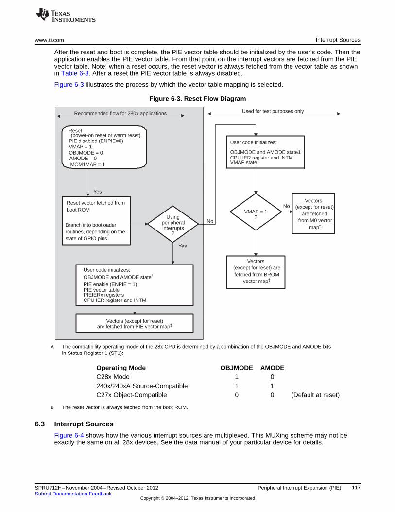
Reset(power-on reset or warm reset)
Reset vector fetched fromboot ROM
Branch into bootloaderroutines, depending on thestate of GPIO pins
Yes
Usingperipheralinterrupts
?
PIE disabled (ENPIE=0)
OBJMODE = 0AMODE = 0
Yes
User code initializes:OBJMODE and AMODE state†
PIE enable (ENPIE = 1)
CPU IER register and INTM
Vectors (except for reset)are fetched from PIE vector map‡
Recommended flow for 280x applications
No
User code initializes:
OBJMODE and AMODE state1CPU IER register and INTMVMAP state
VMAP = 1?
Vectors(except for reset)
are fetched from M0 vector
map‡
Vectors
Used for test purposes only
No
PIE vector tablePIEIERx registers
VMAP = 1
MOM1MAP = 1
(except for reset) arefetched from BROM
vector map‡
www.ti.com Interrupt Sources
After the reset and boot is complete, the PIE vector table should be initialized by the user's code. Then theapplication enables the PIE vector table. From that point on the interrupt vectors are fetched from the PIEvector table. Note: when a reset occurs, the reset vector is always fetched from the vector table as shownin Table 6-3. After a reset the PIE vector table is always disabled.
Figure 6-3 illustrates the process by which the vector table mapping is selected.
Figure 6-3. Reset Flow Diagram
A The compatibility operating mode of the 28x CPU is determined by a combination of the OBJMODE and AMODE bitsin Status Register 1 (ST1):
Operating Mode OBJMODE AMODEC28x Mode 1 0240x/240xA Source-Compatible 1 1C27x Object-Compatible 0 0 (Default at reset)
B The reset vector is always fetched from the boot ROM.
6.3 Interrupt Sources
Figure 6-4 shows how the various interrupt sources are multiplexed. This MUXing scheme may not beexactly the same on all 28x devices. See the data manual of your particular device for details.
117SPRU712H–November 2004–Revised October 2012 Peripheral Interrupt Expansion (PIE)Submit Documentation Feedback
Copyright © 2004–2012, Texas Instruments Incorporated

XINT2
C28
CPU
CPU TIMER 2 (for TI/RTOS)
CPU TIMER 0
Watchdog
Peripherals
(SPI, SCI, I2C, eCAN, ePWM, eCAP, eQEP, ADC)
TINT0
Interrupt Control
XNMICR(15:0)
XINT1Interrupt Control
XINT1
XINT1CR(15:0)
Interrupt ControlXINT2
XINT2CR(15:0)
GPIO
MUX
WDINT
INT1 to
INT12
INT13
INT14
NMI
XINT1CTR(15:0)
XINT2CTR(15:0)
XNMICTR(15:0)
CPU TIMER 1
TINT2
Low Power ModesLPMINT
WAKEINT
TINT1
int13_select
XNMI_XINT13
GPIO0.int
GPIO31.int
ADCXINT2SOC
GPIOXINT1SEL(4:0)
GPIOXINT2SEL(4:0)
GPIOXNMISEL(4:0)
nmi_select
1
MU
XM
UX
PIE
96 Inte
rrupts
MU
XM
UX MU
X
Interrupt Sources www.ti.com
Figure 6-4. External and PIE Interrupt Sources
A In the GPIO MUX, the XINT1, XINT2, and XNMI signals are synchronized and optionally qualified by a user-programmable number of clock cycles. This filters out glitches from the input source. See the GPIO MUX informationin Section 4.5 for details.
118 Peripheral Interrupt Expansion (PIE) SPRU712H–November 2004–Revised October 2012Submit Documentation Feedback
Copyright © 2004–2012, Texas Instruments Incorporated
www.ti.com Interrupt Sources
6.3.1 Procedure for Handling Multiplexed Interrupts
The PIE module multiplexes eight peripheral and external pin interrupts into one CPU interrupt. Theseinterrupts are divided into 12 groups: PIE group 1 - PIE group 12. Each group has an associated enablePIEIER and flag PIEIFR register. These registers are used to control the flow of interrupts to the CPU. ThePIE module also uses the PIEIER and PIEIFR registers to decode to which interrupt service routine theCPU should branch.
There are three main rules that should be followed when clearing bits within the PIEIFR and the PIEIERregisters:
Rule 1: Never clear a PIEIFR bit by software
An incoming interrupt may be lost while a write or a read-modify-write operation to the PIEIFR registertakes place. To clear a PIEIFR bit, the pending interrupt must be serviced. If you want to clear the PIEIFRbit without executing the normal service routine, then use the following procedure:
1. Set the EALLOW bit to allow modification to the PIE vector table.
2. Modify the PIE vector table so that the vector for the peripheral's service routine points to a temporaryISR. This temporary ISR will only perform a return from interrupt (IRET) operation.
3. Enable the interrupt so that the interrupt will be serviced by the temporary ISR.
4. After the temporary interrupt routine is serviced, the PIEIFR bit will be clear
5. Modify the PIE vector table to re-map the peripheral's service routine to the proper service routine.
6. Clear the EALLOW bit.
Rule 2: Procedure for software-prioritizing interrupts
Use the method found in C280x C/C++ Header Files and Peripheral Examples in C (literature numberSPRC191).
(a) Use the CPU IER register as a global priority and the individual PIEIER registers for group priorities. Inthis case the PIEIER register is only modified within an interrupt. In addition, only the PIEIER for thesame group as the interrupt being serviced is modified. This modification is done while the PIEACK bitholds additional interrupts back from the CPU.
(b) Never disable a PIEIER bit for a group when servicing an interrupt from an unrelated group.
Rule 3: Disabling interrupts using PIEIER
If the PIEIER registers are used to enable and then later disable an interrupt then the procedure describedin Section 6.3.2 must be followed.
119SPRU712H–November 2004–Revised October 2012 Peripheral Interrupt Expansion (PIE)Submit Documentation Feedback
Copyright © 2004–2012, Texas Instruments Incorporated

Interrupt Sources www.ti.com
6.3.2 Procedures for Enabling And Disabling Multiplexed Peripheral Interrupts
The proper procedure for enabling or disabling an interrupt is by using the peripheral interruptenable/disable flags. The primary purpose of the PIEIER and CPU IER registers is for softwareprioritization of interrupts within the same PIE interrupt group. The software package C280x C/C++Header Files and Peripheral Examples in C (literature number SPRC191) includes an example thatillustrates this method of software prioritizing interrupts.
Should bits within the PIEIER registers need to be cleared outside of this context, one of the following twoprocedures should be followed. The first method preserves the associated PIE flag register so thatinterrupts are not lost. The second method clears the associated PIE flag register.
Method 1: Use the PIEIERx register to disable the interrupt and preserve the associated PIEIFRxflags.
To clear bits within a PIEIERx register while preserving the associated flags in the PIEIFRx register, thefollowing procedure should be followed:
Step a. Disable global interrupts (INTM = 1).
Step b. Clear the PIEIERx.y bit to disable the interrupt for a given peripheral. This can be done forone or more peripherals within the same group.
Step c. Wait 5 cycles. This delay is required to be sure that any interrupt that was incoming to theCPU has been flagged within the CPU IFR register.
Step d. Clear the CPU IFRx bit for the peripheral group. This is a safe operation on the CPU IFRregister.
Step e. Clear the PIEACKx bit for the peripheral group.
Step f. Enable global interrupts (INTM = 0).
Method 2: Use the PIEIERx register to disable the interrupt and clear the associated PIEIFRx flags.
To perform a software reset of a peripheral interrupt and clear the associated flag in the PIEIFRx registerand CPU IFR register, the following procedure should be followed:
Step 1. Disable global interrupts (INTM = 1).
Step 2. Set the EALLOW bit.
Step 3. Modify the PIE vector table to temporarily map the vector of the specific peripheral interrupt toa empty interrupt service routine (ISR). This empty ISR will only perform a return frominterrupt (IRET) instruction. This is the safe way to clear a single PIEIFRx.y bit without losingany interrupts from other peripherals within the group.
Step 4. Disable the peripheral interrupt at the peripheral register.
Step 5. Enable global interrupts (INTM = 0).
Step 6. Wait for any pending interrupt from the peripheral to be serviced by the empty ISR routine.
Step 7. Disable global interrupts (INTM = 1).
Step 8. Modify the PIE vector table to map the peripheral vector back to its original ISR.
Step 9. Clear the EALLOW bit.
Step 10. Disable the PIEIER bit for given peripheral.
Step 11. Clear the IFR bit for given peripheral group (this is safe operation on CPU IFR register).
Step 12. Clear the PIEACK bit for the PIE group.
Step 13. Enable global interrupts.
120 Peripheral Interrupt Expansion (PIE) SPRU712H–November 2004–Revised October 2012Submit Documentation Feedback
Copyright © 2004–2012, Texas Instruments Incorporated

PeripheralIE/IF
PIEIFRx.1latch
PIEinterrupt
flag
PIEIERx.1
Highest
Vector
01
01
PIEIFRx.8
Vector
latch
PeripheralIE/IF
10
10
Lowest
PIEIERx.8
8 interruptsper group
Search orderhighest to
lowest
Pulsegen
PIEACKx
01
1
2
3a
interruptenable
PIE
3b
4
Vector is fetchedonly after CPUinterrupt logic
has recognizedthe interrupt
9
IFRxlatch
1=valid Int
IERx
10
5
6
10
INTM
7
CPUinterrupt
logic
8
CPU
PIE groupacknowledge
www.ti.com Interrupt Sources
6.3.3 Flow of a Multiplexed Interrupt Request From a Peripheral to the CPU
Figure 6-5 shows the flow with the steps shown in circled numbers. Following the diagram, the steps aredescribed.
Figure 6-5. Multiplexed Interrupt Request Flow Diagram
Step 1. Any peripheral or external interrupt within the PIE group generates an interrupt. If interruptsare enabled within the peripheral module then the interrupt request is sent to the PIE module.
Step 2. The PIE module recognizes that interrupt y within PIE group x (INTx.y) has asserted aninterrupt and the appropriate PIE interrupt flag bit is latched: PIEIFRx.y = 1.
Step 3. For the interrupt request to be sent from the PIE to the CPU, both of the following conditionsmust be true:
(a) The proper enable bit must be set (PIEIERx.y = 1) and
(b) The PIEACKx bit for the group must be clear.
Step 4. If both conditions in 3a and 3b are true, then an interrupt request is sent to the CPU and theacknowledge bit is again set (PIEACKx = 1). The PIEACKx bit will remain set until you clear itto indicate that additional interrupts from the group can be sent from the PIE to the CPU.
Step 5. The CPU interrupt flag bit is set (CPU IFRx = 1) to indicate a pending interrupt x at the CPUlevel.
Step 6. If the CPU interrupt is enabled (CPU IER bit x = 1, or DBGIER bit x = 1) AND the globalinterrupt mask is clear (INTM = 0) then the CPU will service the INTx.
Step 7. The CPU recognizes the interrupt and performs the automatic context save, clears the IERbit, sets INTM, and clears EALLOW. All of the steps that the CPU takes in order to prepare toservice the interrupt are documented in the TMS320C28x DSP CPU and Instruction SetReference Guide (literature number SPRU430).
Step 8. The CPU will then request the appropriate vector from the PIE.
Step 9. For multiplexed interrupts, the PIE module uses the current value in the PIEIERx andPIEIFRx registers to decode which vector address should be used. There are two possiblecases:
(a) The vector for the highest priority interrupt within the group that is both enabled in the
121SPRU712H–November 2004–Revised October 2012 Peripheral Interrupt Expansion (PIE)Submit Documentation Feedback
Copyright © 2004–2012, Texas Instruments Incorporated

Interrupt Sources www.ti.com
PIEIERx register, and flagged as pending in the PIEIFRx is fetched and used as thebranch address. In this manner if an even higher priority enabled interrupt was flaggedafter Step 7, it will be serviced first.
(b) If no flagged interrupts within the group are enabled, then the PIE will respond with thevector for the highest priority interrupt within that group. That is the branch address usedfor INTx.1. This behavior corresponds to the 28x TRAP or INT instructions.
NOTE: Because the PIEIERx register is used to determine which vector will be used for the branch,you must take care when clearing bits within the PIEIERx register. The proper procedure forclearing bits within a PIEIERx register is described in Section 6.3.2. Failure to follow thesesteps can result in changes occurring to the PIEIERx register after an interrupt has beenpassed to the CPU at Step 5 in Figure 6-5. In this case, the PIE will respond as if a TRAP orINT instruction was executed unless there are other interrupts both pending and enabled.
At this point, the PIEIFRx.y bit is cleared and the CPU branches to the vector of the interrupt fetchedfrom the PIE.
6.3.4 The PIE Vector Table
The PIE vector table (see Table 6-6) consists of a 256 x 16 SARAM block that can also be used as RAM(in data space only) if the PIE block is not in use. The PIE vector table contents are undefined on reset.The CPU fixes interrupt priority for INT1 to INT12. The PIE controls priority for each group of eightinterrupts. For example, if INT1.1 should occur simultaneously with INT8.1, both interrupts are presentedto the CPU simultaneously by the PIE block, and the CPU services INT1.1 first. If INT1.1 should occursimultaneously with INT1.8, then INT1.1 is sent to the CPU first and then INT1.8 follows. Interruptprioritization is performed during the vector fetch portion of the interrupt processing.
When the PIE is enabled, a TRAP #1 through TRAP #12 or an INTR INT1 to INTR INT12 instructiontransfers program control to the interrupt service routine corresponding to the first vector within the PIEgroup. For example: TRAP #1 fetches the vector from INT1.1, TRAP #2 fetches the vector from INT2.1and so forth. Similarly an OR IFR, #16-bit operation causes the vector to be fetched from INTR1.1 toINTR12.1 locations, if the respective interrupt flag is set. All other TRAP, INTR, OR IFR,#16-bit operationsfetch the vector from the respective table location. The vector table is EALLOW protected.
The TRAP #0 operation attempts to transfer program control to the address where the reset vector points.The PIE vector table does not, however, include a reset vector and in this case, TRAP #0 returns a valueof 0x000000. Therefore, TRAP #0 should not be used when the PIE is enabled. Doing so will result inundefined behavior.
Out of the 96 possible MUXed interrupts in Table 6-4, 43 interrupts are currently used. The remaininginterrupts are reserved for future devices. These reserved interrupts can be used as software interrupts ifthey are enabled at the PIEIFRx level, provided none of the interrupts within the group is being used by aperipheral. Otherwise, interrupts coming from peripherals may be lost by accidentally clearing their flagswhen modifying the PIEIFR.
To summarize, there are two safe cases when the reserved interrupts can be used as software interrupts:
1. No peripheral within the group is asserting interrupts.
2. No peripheral interrupts are assigned to the group. For example, PIE group 11 and 12 do not have anyperipherals attached to them.
The interrupt grouping for peripherals and external interrupts connected to the PIE module is shown inTable 6-4. Each row in the table shows the 8 interrupts multiplexed into a particular CPU interrupt. Theentire PIE vector table, including both MUXed and non-MUXed interrupts, is shown in Table 6-6.
122 Peripheral Interrupt Expansion (PIE) SPRU712H–November 2004–Revised October 2012Submit Documentation Feedback
Copyright © 2004–2012, Texas Instruments Incorporated

www.ti.com Interrupt Sources
Table 6-4. 280x, 2801x PIE MUXed Peripheral Interrupt Vector Table
INTx.8 INTx.7 INTx.6 INTx.5 INTx.4 INTx.3 INTx.2 INTx.1
INT1.y WAKEINT TINT0 ADCINT XINT2 XINT1 Reserved SEQ2INT SEQ1INT
(LPM/WD) (TIMER 0) (ADC) - (ADC) (ADC)
0xD4E 0xD4C 0xD4A 0xD48 0xD46 0xD44 0xD42 0xD40
INT2.y Reserved Reserved EPWM6_ TZINT EPWM5_TZINT EPWM4_TZINT EPWM3_TZINT EPWM2_TZINT EPWM1_TZINT
- - (ePWM6) (ePWM5) (ePWM4) (ePWM3) (ePWM2) (ePWM1)
0xD5E 0xD5C 0xD5A 0xD58 0xD56 0xD54 0xD52 0xD50
INT3.y Reserved Reserved EPWM6_ INT EPWM5_INT EPWM4_INT EPWM3_INT EPWM2_INT EPWM1_INT
- - (ePWM6) (ePWM5) (ePWM4) (ePWM3) (ePWM2) (ePWM1)
0xD6E 0xD6C 0xD6A 0xD68 0xD66 0xD64 0xD62 0xD60
INT4.y Reserved Reserved Reserved Reserved ECAP4_INT ECAP3_INT ECAP2_INT ECAP1_INT
- - - - (eCAP4) (eCAP3) (eCAP2) (eCAP1)
0xD7E 0xD7C 0xD7A 0xD78 0xD76 0xD74 0xD72 0xD70
INT5.y Reserved Reserved Reserved Reserved Reserved Reserved EQEP2_INT EQEP1_INT
- - - - - - (eQEP2) (eQEP1)
0xD8E 0xD8C 0xD8A 0xD88 0xD86 0xD84 0xD82 0xD80
INT6.y SPITXINTD SPIRXINTD SPITXINTC SPIRXINTC SPITXINTB SPIRXINTB SPITXINTA SPIRXINTA
(SPI-D) (SPI-D) (SPI-C) (SPI-C) (SPI-B) (SPI-B) (SPI-A) (SPI-A)
0xD9E 0xD9C 0xD9A 0xD98 0xD96 0xD94 0xD92 0xD90
INT7.y Reserved Reserved Reserved Reserved Reserved Reserved Reserved Reserved
0xDAE 0xDAC 0xDAA 0xDA8 0xDA6 0xDA4 0xDA2 0xDA0
INT8.y Reserved Reserved Reserved Reserved Reserved Reserved I2CINT2A I2CINT1A
- - - - - - (I2C-A) (I2C-A)
0xDBE 0xDBC 0xDBA 0xDB8 0xDB6 0xDB4 0xDB2 0xDB0
INT9.y ECAN1INTB ECAN0INTB ECAN1INTA ECAN0INTA SCITXINTB SCIRXINTB SCITXINTA SCIRXINTA
(CAN-B) (CAN-B) (CAN-A) (CAN-A) (SCI-B) (SCI-B) (SCI-A) (SCI-A)
0xDCE 0xDCC 0xDCA 0xDC8 0xDC6 0xDC4 0xDC2 0xDC0
INT10.y Reserved Reserved Reserved Reserved Reserved Reserved Reserved Reserved
0xDDE 0xDDC 0xDDA 0xDD8 0xDD6 0xDD4 0xDD2 0xDD0
INT11.y Reserved Reserved Reserved Reserved Reserved Reserved Reserved Reserved
0xDEE 0xDEC 0xDEA 0xDE8 0xDE6 0xDE4 0xDE2 0xDE0
INT12.y Reserved Reserved Reserved Reserved Reserved Reserved Reserved Reserved
0xDFE 0xDFC 0xDFA 0xDF8 0xDF6 0xDF4 0xDF2 0xDF0
123SPRU712H–November 2004–Revised October 2012 Peripheral Interrupt Expansion (PIE)Submit Documentation Feedback
Copyright © 2004–2012, Texas Instruments Incorporated

Interrupt Sources www.ti.com
Table 6-5. 28044 PIE MUXed Peripheral Interrupt Vector Table
INTx.8 INTx.7 INTx.6 INTx.5 INTx.4 INTx.3 INTx.2 INTx.1
INT1.y WAKEINT TINT0 ADCINT XINT2 XINT1 Reserved SEQ2INT SEQ1INT
(LPM/WD) (TIMER 0) (ADC) - - - (ADC) (ADC)
0xD4E 0xD4C 0xD4A 0xD48 0xD46 0xD44 0xD42 0xD40
INT2.y EPWM8_TZINT EPWM7_TZINT EPWM6_ TZINT EPWM5_TZINT EPWM4_TZINT EPWM3_TZINT EPWM2_TZINT EPWM1_TZINT
(ePWM8) (ePWM7) (ePWM6) (ePWM5) (ePWM4) (ePWM3) (ePWM2) (ePWM1)
0xD5E 0xD5C 0xD5A 0xD58 0xD56 0xD54 0xD52 0xD50
INT3.y EPWM8_INT EPWM7_INT EPWM6_ INT EPWM5_INT EPWM4_INT EPWM3_INT EPWM2_INT EPWM1_INT
(ePWM8) (ePWM7) (ePWM6) (ePWM5) (ePWM4) (ePWM3) (ePWM2) (ePWM1)
0xD6E 0xD6C 0xD6A 0xD68 0xD66 0xD64 0xD62 0xD60
INT4.y Reserved Reserved Reserved Reserved Reserved Reserved Reserved Reserved
INT5.y Reserved Reserved Reserved Reserved Reserved Reserved Reserved Reserved
INT6.y Reserved Reserved Reserved Reserved Reserved Reserved SPITXINTA SPIRXINTA
- - - - - - (SPI-A) (SPI-A)
0xD9E 0xD9C 0xD9A 0xD98 0xD96 0xD94 0xD92 0xD90
INT7.y Reserved Reserved Reserved Reserved Reserved Reserved Reserved Reserved
INT8.y Reserved Reserved Reserved Reserved Reserved Reserved I2CINT2A I2CINT1A
- - - - - - (I2C-A) (I2C-A)
0xDBE 0xDBC 0xDBA 0xDB8 0xDB6 0xDB4 0xDB2 0xDB0
INT9.y Reserved Reserved Reserved Reserved Reserved Reserved SCITXINTA SCIRXINTA
(CAN-B) (CAN-B) (CAN-A) (CAN-A) (SCI-B) (SCI-B) (SCI-A) (SCI-A)
0xDCE 0xDCC 0xDCA 0xDC8 0xDC6 0xDC4 0xDC2 0xDC0
INT10.y EPWM16_TZINT EPWM15_TZINT EPWM14_TZINT EPWM13_TZINT EPWM12_TZINT EPWM11_TZINT EPWM10_TZINT EPWM9_TZINT
(ePWM16) (ePWM15) 0xDDA 0xDD8 0xDD6 0xDD4 0xDD2 0xDD0
INT11.y EPWM16_INT EPWM15_INT EPWM14_INT EPWM13_INT EPWM12_INT EPWM11_INT EPWM10_INT EPWM9_INT
(ePWM16) (ePWM15) 0xDEA 0xDE8 0xDE6 0xDE4 0xDE2 0xDE0
INT12.y Reserved Reserved Reserved Reserved Reserved Reserved Reserved Reserved
0xDFE 0xDFC 0xDFA 0xDF8 0xDF6 0xDF4 0xDF2 0xDF0
124 Peripheral Interrupt Expansion (PIE) SPRU712H–November 2004–Revised October 2012Submit Documentation Feedback
Copyright © 2004–2012, Texas Instruments Incorporated
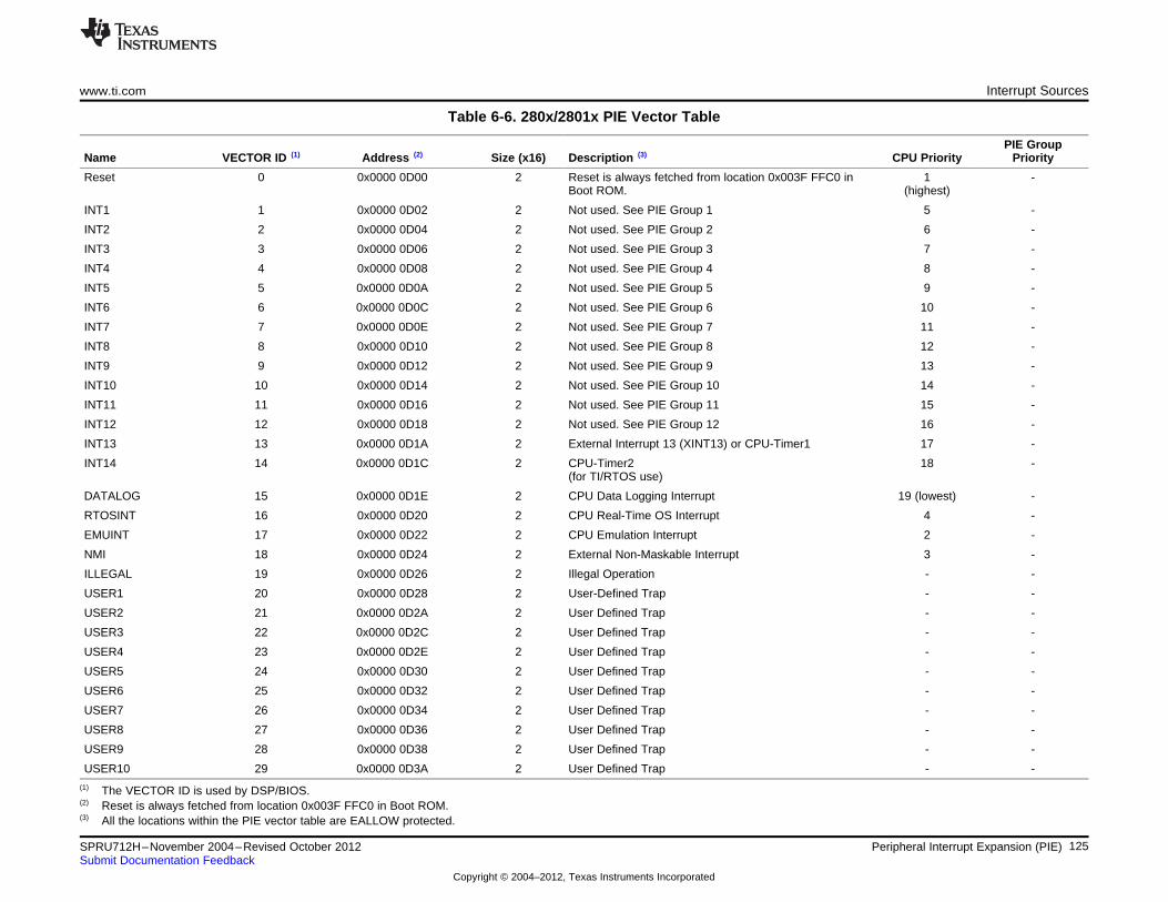
www.ti.com Interrupt Sources
Table 6-6. 280x/2801x PIE Vector Table
PIE GroupName VECTOR ID (1) Address (2) Size (x16) Description (3) CPU Priority Priority
Reset 0 0x0000 0D00 2 Reset is always fetched from location 0x003F FFC0 in 1 -Boot ROM. (highest)
INT1 1 0x0000 0D02 2 Not used. See PIE Group 1 5 -
INT2 2 0x0000 0D04 2 Not used. See PIE Group 2 6 -
INT3 3 0x0000 0D06 2 Not used. See PIE Group 3 7 -
INT4 4 0x0000 0D08 2 Not used. See PIE Group 4 8 -
INT5 5 0x0000 0D0A 2 Not used. See PIE Group 5 9 -
INT6 6 0x0000 0D0C 2 Not used. See PIE Group 6 10 -
INT7 7 0x0000 0D0E 2 Not used. See PIE Group 7 11 -
INT8 8 0x0000 0D10 2 Not used. See PIE Group 8 12 -
INT9 9 0x0000 0D12 2 Not used. See PIE Group 9 13 -
INT10 10 0x0000 0D14 2 Not used. See PIE Group 10 14 -
INT11 11 0x0000 0D16 2 Not used. See PIE Group 11 15 -
INT12 12 0x0000 0D18 2 Not used. See PIE Group 12 16 -
INT13 13 0x0000 0D1A 2 External Interrupt 13 (XINT13) or CPU-Timer1 17 -
INT14 14 0x0000 0D1C 2 CPU-Timer2 18 -(for TI/RTOS use)
DATALOG 15 0x0000 0D1E 2 CPU Data Logging Interrupt 19 (lowest) -
RTOSINT 16 0x0000 0D20 2 CPU Real-Time OS Interrupt 4 -
EMUINT 17 0x0000 0D22 2 CPU Emulation Interrupt 2 -
NMI 18 0x0000 0D24 2 External Non-Maskable Interrupt 3 -
ILLEGAL 19 0x0000 0D26 2 Illegal Operation - -
USER1 20 0x0000 0D28 2 User-Defined Trap - -
USER2 21 0x0000 0D2A 2 User Defined Trap - -
USER3 22 0x0000 0D2C 2 User Defined Trap - -
USER4 23 0x0000 0D2E 2 User Defined Trap - -
USER5 24 0x0000 0D30 2 User Defined Trap - -
USER6 25 0x0000 0D32 2 User Defined Trap - -
USER7 26 0x0000 0D34 2 User Defined Trap - -
USER8 27 0x0000 0D36 2 User Defined Trap - -
USER9 28 0x0000 0D38 2 User Defined Trap - -
USER10 29 0x0000 0D3A 2 User Defined Trap - -
(1) The VECTOR ID is used by DSP/BIOS.(2) Reset is always fetched from location 0x003F FFC0 in Boot ROM.(3) All the locations within the PIE vector table are EALLOW protected.
125SPRU712H–November 2004–Revised October 2012 Peripheral Interrupt Expansion (PIE)Submit Documentation Feedback
Copyright © 2004–2012, Texas Instruments Incorporated

Interrupt Sources www.ti.com
Table 6-6. 280x/2801x PIE Vector Table (continued)
PIE GroupName VECTOR ID (1) Address (2) Size (x16) Description (3) CPU Priority Priority
USER11 30 0x0000 0D3C 2 User Defined Trap - -
USER12 31 0x0000 0D3E 2 User Defined Trap - -
PIE Group 1 Vectors - MUXed into CPU INT1
INT1.1 32 0x0000 0D40 2 SEQ1INT (ADC) 5 1 (highest)
INT1.2 33 0x0000 0D42 2 SEQ2INT (ADC) 5 2
INT1.3 34 0x0000 0D44 2 reserved 5 3
INT1.4 35 0x0000 0D46 2 XINT1 5 4
INT1.5 36 0x0000 0D48 2 XINT2 5 5
INT1.6 37 0x0000 0D4A 2 ADCINT (ADC) 5 6
INT1.7 38 0x0000 0D4C 2 TINT0 (CPU- 5 7Timer0)
INT1.8 39 0x0000 0D4E 2 WAKEINT (LPM/WD) 5 8 (lowest)
PIE Group 2 Vectors - MUXed into CPU INT2
INT2.1 40 0x0000 0D50 2 EPWM1_TZINT (EPWM1) 6 1 (highest)
INT2.2 41 0x0000 0D52 2 EPWM2_TZINT (EPWM2) 6 2
INT2.3 42 0x0000 0D54 2 EPWM3_TZINT (EPWM3) 6 3
INT2.4 43 0x0000 0D56 2 EPWM4_TZINT (EPWM4) 6 4
INT2.5 44 0x0000 0D58 2 EPWM5_TZINT (EPWM5) 6 5
INT2.6 45 0x0000 0D5A 2 EPWM6_TZINT (EPWM6) 6 6
INT2.7 46 0x0000 0D5C 2 Reserved 6 7
INT2.8 47 0x0000 0D5E 2 Reserved 6 8 (lowest)
PIE Group 3 Vectors - MUXed into CPU INT3
INT3.1 48 0x0000 0D60 2 EPWM1_INT (EPWM1) 7 1 (highest)
INT3.2 49 0x0000 0D62 2 EPWM2_INT (EPWM2) 7 2
INT3.3 50 0x0000 0D64 2 EPWM3_INT (EPWM3) 7 3
INT3.4 51 0x0000 0D66 2 EPWM4_INT (EPWM4) 7 4
INT3.5 52 0x0000 0D68 2 EPWM5_INT (EPWM5) 7 5
INT3.6 53 0x0000 0D6A 2 EPWM6_INT (EPWM6) 7 6
INT3.7 54 0x0000 0D6C 2 reserved 7 7
INT3.8 55 0x0000 0D6E 2 reserved 7 8 (lowest)
PIE Group 4 Vectors - MUXed into CPU INT4
INT4.1 56 0x0000 0D70 2 ECAP1_INT (ECAP1) 8 1 (highest)
INT4.2 57 0x0000 0D72 2 ECAP2_INT (ECAP2) 8 2
126 Peripheral Interrupt Expansion (PIE) SPRU712H–November 2004–Revised October 2012Submit Documentation Feedback
Copyright © 2004–2012, Texas Instruments Incorporated

www.ti.com Interrupt Sources
Table 6-6. 280x/2801x PIE Vector Table (continued)
PIE GroupName VECTOR ID (1) Address (2) Size (x16) Description (3) CPU Priority Priority
INT4.3 58 0x0000 0D74 2 ECAP3_INT (ECAP3) 8 3
INT4.4 59 0x0000 0D76 2 ECAP4_INT (ECAP4) 8 4
INT4.5 60 0x0000 0D78 2 Reserved 8 5
INT4.6 61 0x0000 0D7A 2 Reserved 8 6
INT4.7 62 0x0000 0D7C 2 Reserved 8 7
INT4.8 63 0x0000 0D7E 2 Reserved 8 8 (lowest)
PIE Group 5 Vectors - MUXed into CPU INT5
INT5.1 64 0x0000 0D80 2 EQEP1_INT (EQEP1) 9 1 (highest)
INT5.2 65 0x0000 0D82 2 EQEP2_INT (EQEP2) 9 2
INT5.3 66 0x0000 0D84 2 Reserved 9 3
INT5.4 67 0x0000 0D86 2 Reserved 9 4
INT5.5 68 0x0000 0D88 2 Reserved 9 5
INT5.6 69 0x0000 0D8A 2 Reserved 9 6
INT5.7 70 0x0000 0D8C 2 Reserved 9 7
INT5.8 71 0x0000 0D8E 2 Reserved 9 8 (lowest)
PIE Group 6 Vectors - MUXed into CPU INT6
INT6.1 72 0x0000 0D90 2 SPIRXINTA (SPI-A) 10 1 (highest)
INT6.2 73 0x0000 0D92 2 SPITXINTA (SPI-A) 10 2
INT6.3 74 0x0000 0D94 2 SPIRXINTB (SPI-B) 10 3
INT6.4 75 0x0000 0D96 2 SPITXINTB (SPI-B) 10 4
INT6.5 76 0x0000 0D98 2 SPIRXINTC (SPI-C) 10 5
INT6.6 77 0x0000 0D9A 2 SPITXINTC (SPI-C) 10 6
INT6.7 78 0x0000 0D9C 2 SPIRXINTD (SPI-D) 10 7
INT6.8 79 0x0000 0D9E 2 SPITXINTD (SPI-D) 10 8 (lowest)
PIE Group 7 Vectors - MUXed into CPU INT7
INT7.1 80 0x0000 0DA0 2 Reserved 11 1 (highest)
INT7.2 81 0x0000 0DA2 2 Reserved 11 2
INT7.3 82 0x0000 0DA4 2 Reserved 11 3
INT7.4 83 0x0000 0DA6 2 Reserved 11 4
INT7.5 84 0x0000 0DA8 2 Reserved 11 5
INT7.6 85 0x0000 0DAA 2 Reserved 11 6
INT7.7 86 0x0000 0DAC 2 Reserved 11 7
INT7.8 87 0x0000 0DAE 2 Reserved 11 8 (lowest)
127SPRU712H–November 2004–Revised October 2012 Peripheral Interrupt Expansion (PIE)Submit Documentation Feedback
Copyright © 2004–2012, Texas Instruments Incorporated

Interrupt Sources www.ti.com
Table 6-6. 280x/2801x PIE Vector Table (continued)
PIE GroupName VECTOR ID (1) Address (2) Size (x16) Description (3) CPU Priority Priority
PIE Group 8 Vectors - MUXed into CPU INT8
INT8.1 88 0x0000 0DB0 2 I2CINT1A I2C-A 12 1 (highest)
INT8.2 89 0x0000 0DB2 2 I2CINT2A I2C-A 12 2
INT8.3 90 0x0000 0DB4 2 Reserved 12 3
INT8.4 91 0x0000 0DB6 2 Reserved 12 4
INT8.5 92 0x0000 0DB8 2 Reserved 12 5
INT8.6 93 0x0000 0DBA 2 Reserved 12 6
INT8.7 94 0x0000 0DBC 2 Reserved 12 7
INT8.8 95 0x0000 0DBE 2 Reserved 12 8 (lowest)
PIE Group 9 Vectors - MUXed into CPU INT9
INT9.1 96 0x0000 0DC0 2 SCIRXINTA (SCI-A) 13 1 (highest)
INT9.2 97 0x0000 0DC2 2 SCITXINTA (SCI-A) 13 2
INT9.3 98 0x0000 0DC4 2 SCIRXINTB (SCI-B) 13 3
INT9.4 99 0x0000 0DC6 2 SCITXINTB (SCI-B) 13 4
INT9.5 100 0x0000 0DC8 2 ECAN0INTA (eCAN-A) 13 5
INT9.6 101 0x0000 0DCA 2 ECAN1INTA (eCAN-A) 13 6
INT9.7 102 0x0000 0DCC 2 ECAN0INTB (eCAN-B) 13 7
INT9.8 103 0x0000 0DCE 2 ECAN1INTB (eCAN-B) 13 8 (lowest)
PIE Group 10 Vectors - MUXed into CPU INT10
INT10.1 104 0x0000 0DD0 2 Reserved 14 1 (highest)
INT10.2 105 0x0000 0DD2 2 Reserved 14 2
INT10.3 106 0x0000 0DD4 2 Reserved 14 3
INT10.4 107 0x0000 0DD6 2 Reserved 14 4
INT10.5 108 0x0000 0DD8 2 Reserved 14 5
INT10.6 109 0x0000 0DDA 2 Reserved 14 6
INT10.7 110 0x0000 0DDC 2 Reserved 14 7
INT10.8 111 0x0000 0DDE 2 Reserved 14 8 (lowest)
PIE Group 11 Vectors - MUXed into CPU INT11
INT11.1 112 0x0000 0DE0 2 Reserved 15 1 (highest)
INT11.2 113 0x0000 0DE2 2 Reserved 15 2
INT11.3 114 0x0000 0DE4 2 Reserved 15 3
INT11.4 115 0x0000 0DE6 2 Reserved 15 4
INT11.5 116 0x0000 0DE8 2 Reserved 15 5
128 Peripheral Interrupt Expansion (PIE) SPRU712H–November 2004–Revised October 2012Submit Documentation Feedback
Copyright © 2004–2012, Texas Instruments Incorporated

www.ti.com Interrupt Sources
Table 6-6. 280x/2801x PIE Vector Table (continued)
PIE GroupName VECTOR ID (1) Address (2) Size (x16) Description (3) CPU Priority Priority
INT11.6 117 0x0000 0DEA 2 Reserved 15 6
INT11.7 118 0x0000 0DEC 2 Reserved 15 7
INT11.8 119 0x0000 0DEE 2 Reserved 15 8 (lowest)
PIE Group 12 Vectors - Muxed into CPU INT12
INT12.1 120 0x0000 0DF0 2 Reserved 16 1 (highest)
INT12.2 121 0x0000 0DF2 2 Reserved 16 2
INT12.3 122 0x0000 0DF4 2 Reserved 16 3
INT12.4 123 0x0000 0DF6 2 Reserved 16 4
INT12.5 124 0x0000 0DF8 2 Reserved 16 5
INT12.6 125 0x0000 0DFA 2 Reserved 16 6
INT12.7 126 0x0000 0DFC 2 Reserved 16 7
INT12.8 127 0x0000 0DFE 2 Reserved 16 8 (lowest)
Table 6-7. 28044 PIE Vector Table
PIE GroupName VECTOR ID (1) Address (2) Size (x16) Description (3) CPU Priority Priority
Reset 0 0x0000 0D00 2 Reset is always fetched from location 0x003F FFC0 in 1 -Boot ROM. (highest)
INT1 1 0x0000 0D02 2 Not used. See PIE Group 1 5 -
INT2 2 0x0000 0D04 2 Not used. See PIE Group 2 6 -
INT3 3 0x0000 0D06 2 Not used. See PIE Group 3 7 -
INT4 4 0x0000 0D08 2 Not used. See PIE Group 4 8 -
INT5 5 0x0000 0D0A 2 Not used. See PIE Group 5 9 -
INT6 6 0x0000 0D0C 2 Not used. See PIE Group 6 10 -
INT7 7 0x0000 0D0E 2 Not used. See PIE Group 7 11 -
INT8 8 0x0000 0D10 2 Not used. See PIE Group 8 12 -
INT9 9 0x0000 0D12 2 Not used. See PIE Group 9 13 -
INT10 10 0x0000 0D14 2 Not used. See PIE Group 10 14 -
INT11 11 0x0000 0D16 2 Not used. See PIE Group 11 15 -
INT12 12 0x0000 0D18 2 Not used. See PIE Group 12 16 -
INT13 13 0x0000 0D1A 2 External Interrupt 13 (XINT13) or CPU-Timer1 17 -
(1) The VECTOR ID is used by DSP/BIOS.(2) Reset is always fetched from location 0x003F FFC0 in Boot ROM.(3) All the locations within the PIE vector table are EALLOW protected.
129SPRU712H–November 2004–Revised October 2012 Peripheral Interrupt Expansion (PIE)Submit Documentation Feedback
Copyright © 2004–2012, Texas Instruments Incorporated

Interrupt Sources www.ti.com
Table 6-7. 28044 PIE Vector Table (continued)
PIE GroupName VECTOR ID (1) Address (2) Size (x16) Description (3) CPU Priority Priority
INT14 14 0x0000 0D1C 2 CPU-Timer2 18 -(for TI/RTOS use)
DATALOG 15 0x0000 0D1E 2 CPU Data Logging Interrupt 19 (lowest) -
RTOSINT 16 0x0000 0D20 2 CPU Real-Time OS Interrupt 4 -
EMUINT 17 0x0000 0D22 2 CPU Emulation Interrupt 2 -
NMI 18 0x0000 0D24 2 External Non-Maskable Interrupt 3 -
ILLEGAL 19 0x0000 0D26 2 Illegal Operation - -
USER1 20 0x0000 0D28 2 User-Defined Trap - -
USER2 21 0x0000 0D2A 2 User Defined Trap - -
USER3 22 0x0000 0D2C 2 User Defined Trap - -
USER4 23 0x0000 0D2E 2 User Defined Trap - -
USER5 24 0x0000 0D30 2 User Defined Trap - -
USER6 25 0x0000 0D32 2 User Defined Trap - -
USER7 26 0x0000 0D34 2 User Defined Trap - -
USER8 27 0x0000 0D36 2 User Defined Trap - -
USER9 28 0x0000 0D38 2 User Defined Trap - -
USER10 29 0x0000 0D3A 2 User Defined Trap - -
USER11 30 0x0000 0D3C 2 User Defined Trap - -
USER12 31 0x0000 0D3E 2 User Defined Trap - -
PIE Group 1 Vectors - MUXed into CPU INT1
INT1.1 32 0x0000 0D40 2 SEQ1INT (ADC) 5 1 (highest)
INT1.2 33 0x0000 0D42 2 SEQ2INT (ADC) 5 2
INT1.3 34 0x0000 0D44 2 reserved 5 3
INT1.4 35 0x0000 0D46 2 XINT1 5 4
INT1.5 36 0x0000 0D48 2 XINT2 5 5
INT1.6 37 0x0000 0D4A 2 ADCINT (ADC) 5 6
INT1.7 38 0x0000 0D4C 2 TINT0 (CPU- 5 7Timer0)
INT1.8 39 0x0000 0D4E 2 WAKEINT (LPM/WD) 5 8 (lowest)
PIE Group 2 Vectors - MUXed into CPU INT2
INT2.1 40 0x0000 0D50 2 EPWM1_TZINT (EPWM1) 6 1 (highest)
INT2.2 41 0x0000 0D52 2 EPWM2_TZINT (EPWM2) 6 2
INT2.3 42 0x0000 0D54 2 EPWM3_TZINT (EPWM3) 6 3
INT2.4 43 0x0000 0D56 2 EPWM4_TZINT (EPWM4) 6 4
130 Peripheral Interrupt Expansion (PIE) SPRU712H–November 2004–Revised October 2012Submit Documentation Feedback
Copyright © 2004–2012, Texas Instruments Incorporated
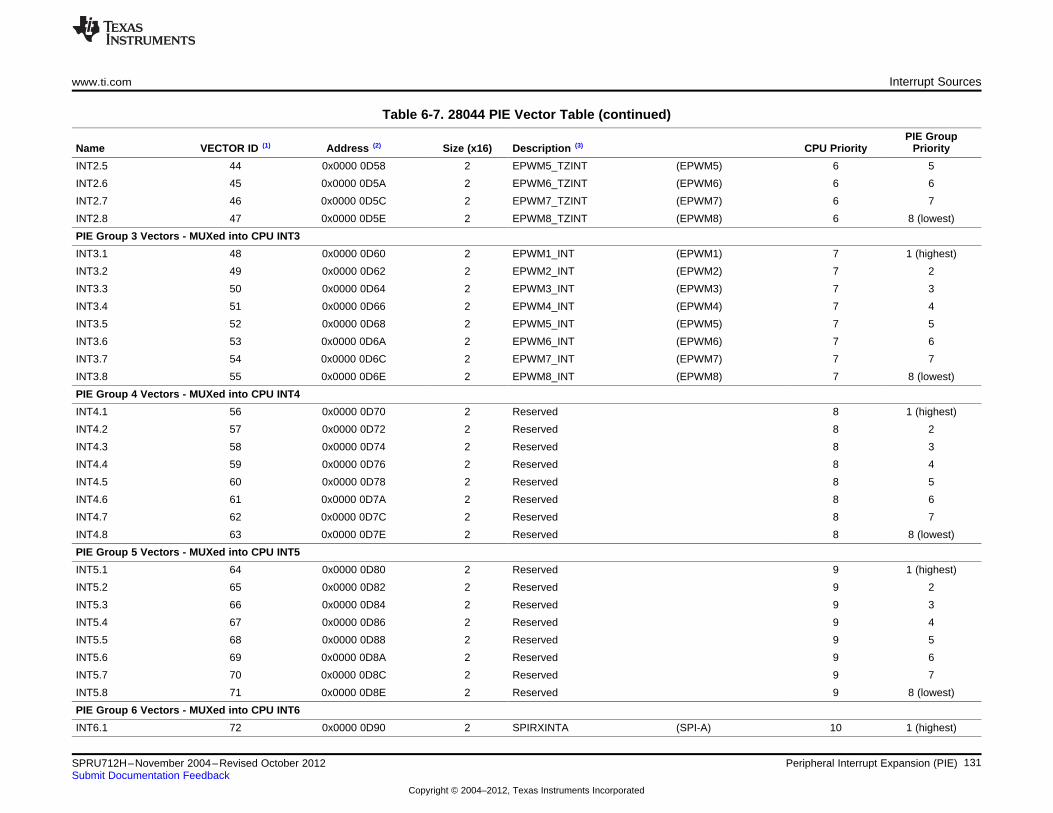
www.ti.com Interrupt Sources
Table 6-7. 28044 PIE Vector Table (continued)
PIE GroupName VECTOR ID (1) Address (2) Size (x16) Description (3) CPU Priority Priority
INT2.5 44 0x0000 0D58 2 EPWM5_TZINT (EPWM5) 6 5
INT2.6 45 0x0000 0D5A 2 EPWM6_TZINT (EPWM6) 6 6
INT2.7 46 0x0000 0D5C 2 EPWM7_TZINT (EPWM7) 6 7
INT2.8 47 0x0000 0D5E 2 EPWM8_TZINT (EPWM8) 6 8 (lowest)
PIE Group 3 Vectors - MUXed into CPU INT3
INT3.1 48 0x0000 0D60 2 EPWM1_INT (EPWM1) 7 1 (highest)
INT3.2 49 0x0000 0D62 2 EPWM2_INT (EPWM2) 7 2
INT3.3 50 0x0000 0D64 2 EPWM3_INT (EPWM3) 7 3
INT3.4 51 0x0000 0D66 2 EPWM4_INT (EPWM4) 7 4
INT3.5 52 0x0000 0D68 2 EPWM5_INT (EPWM5) 7 5
INT3.6 53 0x0000 0D6A 2 EPWM6_INT (EPWM6) 7 6
INT3.7 54 0x0000 0D6C 2 EPWM7_INT (EPWM7) 7 7
INT3.8 55 0x0000 0D6E 2 EPWM8_INT (EPWM8) 7 8 (lowest)
PIE Group 4 Vectors - MUXed into CPU INT4
INT4.1 56 0x0000 0D70 2 Reserved 8 1 (highest)
INT4.2 57 0x0000 0D72 2 Reserved 8 2
INT4.3 58 0x0000 0D74 2 Reserved 8 3
INT4.4 59 0x0000 0D76 2 Reserved 8 4
INT4.5 60 0x0000 0D78 2 Reserved 8 5
INT4.6 61 0x0000 0D7A 2 Reserved 8 6
INT4.7 62 0x0000 0D7C 2 Reserved 8 7
INT4.8 63 0x0000 0D7E 2 Reserved 8 8 (lowest)
PIE Group 5 Vectors - MUXed into CPU INT5
INT5.1 64 0x0000 0D80 2 Reserved 9 1 (highest)
INT5.2 65 0x0000 0D82 2 Reserved 9 2
INT5.3 66 0x0000 0D84 2 Reserved 9 3
INT5.4 67 0x0000 0D86 2 Reserved 9 4
INT5.5 68 0x0000 0D88 2 Reserved 9 5
INT5.6 69 0x0000 0D8A 2 Reserved 9 6
INT5.7 70 0x0000 0D8C 2 Reserved 9 7
INT5.8 71 0x0000 0D8E 2 Reserved 9 8 (lowest)
PIE Group 6 Vectors - MUXed into CPU INT6
INT6.1 72 0x0000 0D90 2 SPIRXINTA (SPI-A) 10 1 (highest)
131SPRU712H–November 2004–Revised October 2012 Peripheral Interrupt Expansion (PIE)Submit Documentation Feedback
Copyright © 2004–2012, Texas Instruments Incorporated
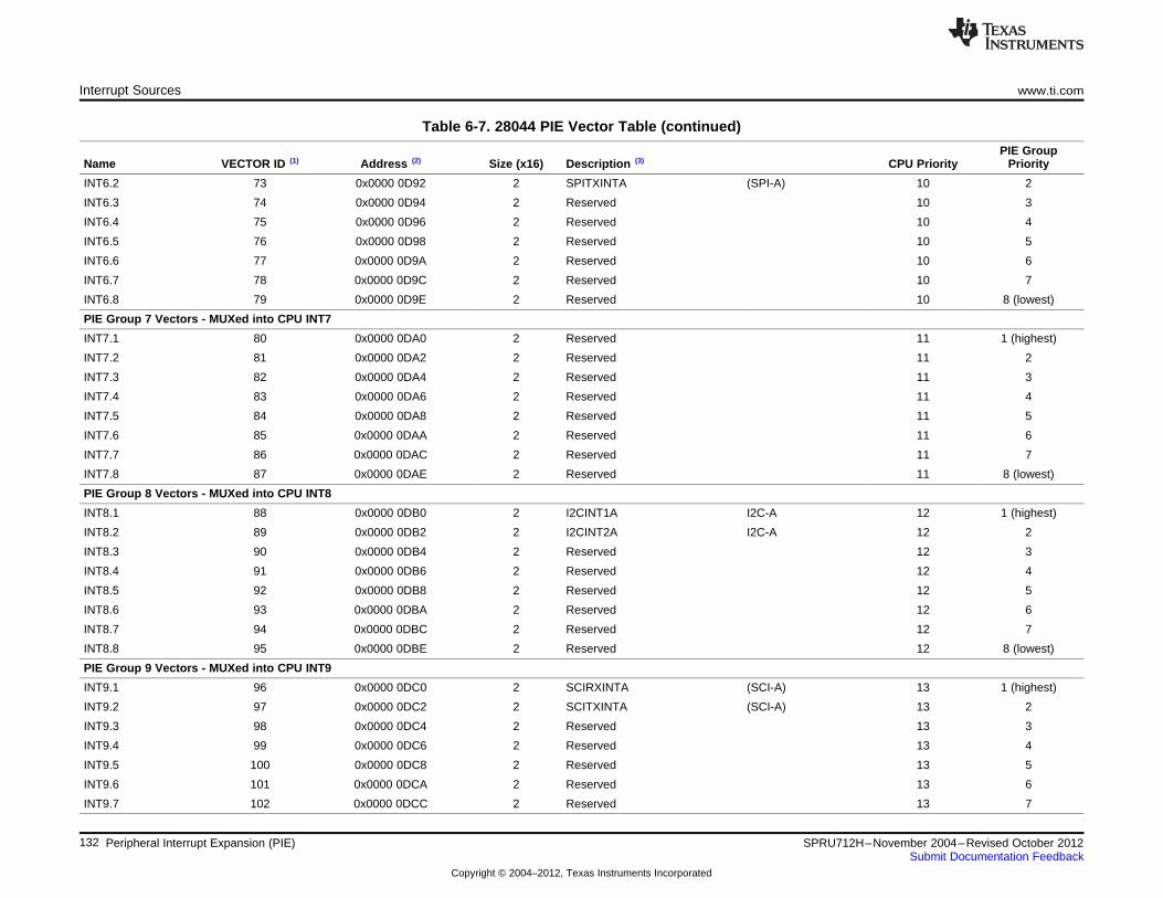
Interrupt Sources www.ti.com
Table 6-7. 28044 PIE Vector Table (continued)
PIE GroupName VECTOR ID (1) Address (2) Size (x16) Description (3) CPU Priority Priority
INT6.2 73 0x0000 0D92 2 SPITXINTA (SPI-A) 10 2
INT6.3 74 0x0000 0D94 2 Reserved 10 3
INT6.4 75 0x0000 0D96 2 Reserved 10 4
INT6.5 76 0x0000 0D98 2 Reserved 10 5
INT6.6 77 0x0000 0D9A 2 Reserved 10 6
INT6.7 78 0x0000 0D9C 2 Reserved 10 7
INT6.8 79 0x0000 0D9E 2 Reserved 10 8 (lowest)
PIE Group 7 Vectors - MUXed into CPU INT7
INT7.1 80 0x0000 0DA0 2 Reserved 11 1 (highest)
INT7.2 81 0x0000 0DA2 2 Reserved 11 2
INT7.3 82 0x0000 0DA4 2 Reserved 11 3
INT7.4 83 0x0000 0DA6 2 Reserved 11 4
INT7.5 84 0x0000 0DA8 2 Reserved 11 5
INT7.6 85 0x0000 0DAA 2 Reserved 11 6
INT7.7 86 0x0000 0DAC 2 Reserved 11 7
INT7.8 87 0x0000 0DAE 2 Reserved 11 8 (lowest)
PIE Group 8 Vectors - MUXed into CPU INT8
INT8.1 88 0x0000 0DB0 2 I2CINT1A I2C-A 12 1 (highest)
INT8.2 89 0x0000 0DB2 2 I2CINT2A I2C-A 12 2
INT8.3 90 0x0000 0DB4 2 Reserved 12 3
INT8.4 91 0x0000 0DB6 2 Reserved 12 4
INT8.5 92 0x0000 0DB8 2 Reserved 12 5
INT8.6 93 0x0000 0DBA 2 Reserved 12 6
INT8.7 94 0x0000 0DBC 2 Reserved 12 7
INT8.8 95 0x0000 0DBE 2 Reserved 12 8 (lowest)
PIE Group 9 Vectors - MUXed into CPU INT9
INT9.1 96 0x0000 0DC0 2 SCIRXINTA (SCI-A) 13 1 (highest)
INT9.2 97 0x0000 0DC2 2 SCITXINTA (SCI-A) 13 2
INT9.3 98 0x0000 0DC4 2 Reserved 13 3
INT9.4 99 0x0000 0DC6 2 Reserved 13 4
INT9.5 100 0x0000 0DC8 2 Reserved 13 5
INT9.6 101 0x0000 0DCA 2 Reserved 13 6
INT9.7 102 0x0000 0DCC 2 Reserved 13 7
132 Peripheral Interrupt Expansion (PIE) SPRU712H–November 2004–Revised October 2012Submit Documentation Feedback
Copyright © 2004–2012, Texas Instruments Incorporated

www.ti.com PIE Configuration Registers
Table 6-7. 28044 PIE Vector Table (continued)
PIE GroupName VECTOR ID (1) Address (2) Size (x16) Description (3) CPU Priority Priority
INT9.8 103 0x0000 0DCE 2 Reserved 13 8 (lowest)
PIE Group 10 Vectors - MUXed into CPU INT10
INT10.1 104 0x0000 0DD0 2 EPWM9_TZINT (ePWM9) 14 1 (highest)
INT10.2 105 0x0000 0DD2 2 EPWM10_TZINT (ePWM10) 14 2
INT10.3 106 0x0000 0DD4 2 EPWM11_TZINT (ePWM11) 14 3
INT10.4 107 0x0000 0DD6 2 EPWM12_TZINT (ePWM12) 14 4
INT10.5 108 0x0000 0DD8 2 EPWM13_TZINT (ePWM13) 14 5
INT10.6 109 0x0000 0DDA 2 EPWM14_TZINT (ePWM14) 14 6
INT10.7 110 0x0000 0DDC 2 EPWM15_TZINT (ePWM15) 14 7
INT10.8 111 0x0000 0DDE 2 EPWM16_TZINT (ePWM16) 14 8 (lowest)
PIE Group 11 Vectors - MUXed into CPU INT11
INT11.1 112 0x0000 0DE0 2 EPWM9_INT (ePWM9) 15 1 (highest)
INT11.2 113 0x0000 0DE2 2 EPWM10_INT (ePWM10) 15 2
INT11.3 114 0x0000 0DE4 2 EPWM11_INT (ePWM11) 15 3
INT11.4 115 0x0000 0DE6 2 EPWM12_INT (ePWM12) 15 4
INT11.5 116 0x0000 0DE8 2 EPWM13_INT (ePWM13) 15 5
INT11.6 117 0x0000 0DEA 2 EPWM14_INT (ePWM14) 15 6
INT11.7 118 0x0000 0DEC 2 EPWM15_INT (ePWM15) 15 7
INT11.8 119 0x0000 0DEE 2 EPWM16_INT (ePWM16) 15 8 (lowest)
PIE Group 12 Vectors - Muxed into CPU INT12
INT12.1 120 0x0000 0DF0 2 Reserved 16 1 (highest)
INT12.2 121 0x0000 0DF2 2 Reserved 16 2
INT12.3 122 0x0000 0DF4 2 Reserved 16 3
INT12.4 123 0x0000 0DF6 2 Reserved 16 4
INT12.5 124 0x0000 0DF8 2 Reserved 16 5
INT12.6 125 0x0000 0DFA 2 Reserved 16 6
INT12.7 126 0x0000 0DFC 2 Reserved 16 7
INT12.8 127 0x0000 0DFE 2 Reserved 16 8 (lowest)
6.4 PIE Configuration Registers
The registers controlling the functionality of the PIE block are shown in Table 6-8.
133SPRU712H–November 2004–Revised October 2012 Peripheral Interrupt Expansion (PIE)Submit Documentation Feedback
Copyright © 2004–2012, Texas Instruments Incorporated

PIE Configuration Registers www.ti.com
Table 6-8. PIE Configuration and Control Registers
Name Address Size (x16) Description
PIECTRL 0x0000-0CE0 1 PIE, Control Register
PIEACK 0x0000-0CE1 1 PIE, Acknowledge Register
PIEIER1 0x0000-0CE2 1 PIE, INT1 Group Enable Register
PIEIFR1 0x0000-0CE3 1 PIE, INT1 Group Flag Register
PIEIER2 0x0000-0CE4 1 PIE, INT2 Group Enable Register
PIEIFR2 0x0000-0CE5 1 PIE, INT2 Group Flag Register
PIEIER3 0x0000-0CE6 1 PIE, INT3 Group Enable Register
PIEIFR3 0x0000-0CE7 1 PIE, INT3 Group Flag Register
PIEIER4 0x0000-0CE8 1 PIE, INT4 Group Enable Register
PIEIFR4 0x0000-0CE9 1 PIE, INT4 Group Flag Register
PIEIER5 0x0000-0CEA 1 PIE, INT5 Group Enable Register
PIEIFR5 0x0000-0CEB 1 PIE, INT5 Group Flag Register
PIEIER6 0x0000-0CEC 1 PIE, INT6 Group Enable Register
PIEIFR6 0x0000-0CED 1 PIE, INT6 Group Flag Register
PIEIER7 0x0000-0CEE 1 PIE, INT7 Group Enable Register
PIEIFR7 0x0000-0CEF 1 PIE, INT7 Group Flag Register
PIEIER8 0x0000-0CF0 1 PIE, INT8 Group Enable Register
PIEIFR8 0x0000-0CF1 1 PIE, INT8 Group Flag Register
PIEIER9 0x0000-0CF2 1 PIE, INT9 Group Enable Register
PIEIFR9 0x0000-0CF3 1 PIE, INT9 Group Flag Register
PIEIER10 0x0000-0CF4 1 PIE, INT10 Group Enable Register
PIEIFR10 0x0000-0CF5 1 PIE, INT10 Group Flag Register
PIEIER11 0x0000-0CF6 1 PIE, INT11 Group Enable Register
PIEIFR11 0x0000-0CF7 1 PIE, INT11 Group Flag Register
PIEIER12 0x0000-0CF8 1 PIE, INT12 Group Enable Register
PIEIFR12 0x0000-0CF9 1 PIE, INT12 Group Flag Register
134 Peripheral Interrupt Expansion (PIE) SPRU712H–November 2004–Revised October 2012Submit Documentation Feedback
Copyright © 2004–2012, Texas Instruments Incorporated

www.ti.com PIE Interrupt Registers
6.5 PIE Interrupt Registers
Figure 6-6. PIECTRL Register (Address CE0)15 1 0
PIEVECT ENPIE
R-0 R/W-0
LEGEND: R/W = Read/Write; R = Read only; -n = value after reset
Table 6-9. PIECTRL Register Address Field Descriptions
Bits Field Value Description
15-1 PIEVECT These bits indicate the address within the PIE vector table from which the vector was fetched. Theleast significant bit of the address is ignored and only bits 1 to 15 of the address is shown. You canread the vector value to determine which interrupt generated the vector fetch.
For Example: If PIECTRL = 0x0D27 then the vector from address 0x0D26 (illegal operation) wasfetched.
0 ENPIE Enable vector fetching from PIE vector table.
Note: The reset vector is never fetched from the PIE, even when it is enabled. This vector is alwaysfetched from boot ROM.
0 If this bit is set to 0, the PIE block is disabled and vectors are fetched from the CPU vector table inboot ROM. All PIE block registers (PIEACK, PIEIFR, PIEIER) can be accessed even when the PIEblock is disabled.
1 When ENPIE is set to 1, all vectors, except for reset, are fetched from the PIE vector table. The resetvector is always fetched from the boot ROM.
Figure 6-7. PIE Interrupt Acknowledge Register (PIEACK) Register (Address CE1)15 12 11 0
Reserved PIEACK
R-0 R/W1C-1
LEGEND: R/W1C = Read/Write 1 to clear; R = Read only; -n = value after reset
Table 6-10. PIE Interrupt Acknowledge Register (PIEACK) Field Descriptions
Bits Field Value Description
15-12 Reserved Reserved
11-0 PIEACK Each bit in PIEACK refers to a specific PIE group. Bit 0 refers to interrupts in PIE group 1 that areMUXed into INT1 up to Bit 11, which refers to PIE group 12 that is MUXed into CPU INT12.
bit x = 0 (1) If a bit reads as a 0, it indicates that the PIE can send an interrupt from the respective group to theCPU.
Writes of 0 are ignored.
bit x = 1 Reading a 1 indicates if an interrupt from the respective group has been sent to the CPU and allother interrupts from the group are currently blocked.
Writing a 1 to the respective interrupt bit clears the bit and enables the PIE block to drive a pulse intothe CPU interrupt input if an interrupt is pending for that group.
(1) bit x = PIEACK bit 0 - PIEACK bit 11. Bit 0 refers to CPU INT1 up to Bit 11, which refers to CPU INT12
6.5.1 PIE Interrupt Flag Registers
There are twelve PIEIFR registers, one for each CPU interrupt used by the PIE module (INT1-INT12).
135SPRU712H–November 2004–Revised October 2012 Peripheral Interrupt Expansion (PIE)Submit Documentation Feedback
Copyright © 2004–2012, Texas Instruments Incorporated
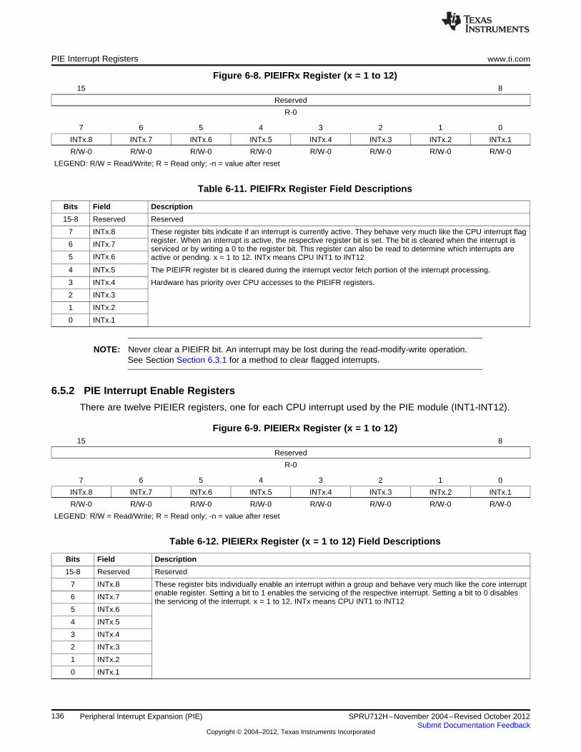
PIE Interrupt Registers www.ti.com
Figure 6-8. PIEIFRx Register (x = 1 to 12)15 8
Reserved
R-0
7 6 5 4 3 2 1 0
INTx.8 INTx.7 INTx.6 INTx.5 INTx.4 INTx.3 INTx.2 INTx.1
R/W-0 R/W-0 R/W-0 R/W-0 R/W-0 R/W-0 R/W-0 R/W-0
LEGEND: R/W = Read/Write; R = Read only; -n = value after reset
Table 6-11. PIEIFRx Register Field Descriptions
Bits Field Description
15-8 Reserved Reserved
7 INTx.8 These register bits indicate if an interrupt is currently active. They behave very much like the CPU interrupt flagregister. When an interrupt is active, the respective register bit is set. The bit is cleared when the interrupt is6 INTx.7serviced or by writing a 0 to the register bit. This register can also be read to determine which interrupts are
5 INTx.6 active or pending. x = 1 to 12. INTx means CPU INT1 to INT12
4 INTx.5 The PIEIFR register bit is cleared during the interrupt vector fetch portion of the interrupt processing.
3 INTx.4 Hardware has priority over CPU accesses to the PIEIFR registers.
2 INTx.3
1 INTx.2
0 INTx.1
NOTE: Never clear a PIEIFR bit. An interrupt may be lost during the read-modify-write operation.See Section Section 6.3.1 for a method to clear flagged interrupts.
6.5.2 PIE Interrupt Enable Registers
There are twelve PIEIER registers, one for each CPU interrupt used by the PIE module (INT1-INT12).
Figure 6-9. PIEIERx Register (x = 1 to 12)15 8
Reserved
R-0
7 6 5 4 3 2 1 0
INTx.8 INTx.7 INTx.6 INTx.5 INTx.4 INTx.3 INTx.2 INTx.1
R/W-0 R/W-0 R/W-0 R/W-0 R/W-0 R/W-0 R/W-0 R/W-0
LEGEND: R/W = Read/Write; R = Read only; -n = value after reset
Table 6-12. PIEIERx Register (x = 1 to 12) Field Descriptions
Bits Field Description
15-8 Reserved Reserved
7 INTx.8 These register bits individually enable an interrupt within a group and behave very much like the core interruptenable register. Setting a bit to 1 enables the servicing of the respective interrupt. Setting a bit to 0 disables6 INTx.7the servicing of the interrupt. x = 1 to 12. INTx means CPU INT1 to INT12
5 INTx.6
4 INTx.5
3 INTx.4
2 INTx.3
1 INTx.2
0 INTx.1
136 Peripheral Interrupt Expansion (PIE) SPRU712H–November 2004–Revised October 2012Submit Documentation Feedback
Copyright © 2004–2012, Texas Instruments Incorporated

www.ti.com PIE Interrupt Registers
NOTE: Care must be taken when clearing PIEIER bits during normal operation. See SectionSection 6.3.2 for the proper procedure for handling these bits.
6.5.3 CPU Interrupt Flag Register (IFR)
The CPU interrupt flag register (IFR), is a 16-bit, CPU register and is used to identify and clear pendinginterrupts. The IFR contains flag bits for all the maskable interrupts at the CPU level (INT1-INT14,DLOGINT and RTOSINT). When the PIE is enabled, the PIE module multiplexes interrupt sources forINT1-INT12.
When a maskable interrupt is requested, the flag bit in the corresponding peripheral control register is setto 1. If the corresponding mask bit is also 1, the interrupt request is sent to the CPU, setting thecorresponding flag in the IFR. This indicates that the interrupt is pending or waiting for acknowledgment.
To identify pending interrupts, use the PUSH IFR instruction and then test the value on the stack. Use theOR IFR instruction to set IFR bits and use the AND IFR instruction to manually clear pending interrupts.All pending interrupts are cleared with the AND IFR #0 instruction or by a hardware reset.
The following events also clear an IFR flag:
• The CPU acknowledges the interrupt.
• The 28x device is reset.
NOTE:1. To clear a CPU IFR bit, you must write a zero to it, not a one.2. When a maskable interrupt is acknowledged, only the IFR bit is cleared automatically.
The flag bit in the corresponding peripheral control register is not cleared. If anapplication requires that the control register flag be cleared, the bit must be cleared bysoftware.
3. When an interrupt is requested by an INTR instruction and the corresponding IFR bit isset, the CPU does not clear the bit automatically. If an application requires that the IFRbit be cleared, the bit must be cleared by software.
4. IMR and IFR registers pertain to core-level interrupts. All peripherals have their owninterrupt mask and flag bits in their respective control/configuration registers. Note thatseveral peripheral interrupts are grouped under one core-level interrupt.
Figure 6-10. Interrupt Flag Register (IFR) — CPU Register15 14 13 12 11 10 9 8
RTOSINT DLOGINT INT14 INT13 INT12 INT11 INT10 INT9
R/W-0 R/W-0 R/W-0 R/W-0 R/W-0 R/W-0 R/W-0 R/W-0
7 6 5 4 3 2 1 0
INT8 INT7 INT6 INT5 INT4 INT3 INT2 INT1
R/W-0 R/W-0 R/W-0 R/W-0 R/W-0 R/W-0 R/W-0 R/W-0
LEGEND: R/W = Read/Write; R = Read only; -n = value after reset
Table 6-13. Interrupt Flag Register (IFR) — CPU Register Field Descriptions
Bits Field Value Description
15 RTOSINT Real-time operating system flag. RTOSINT is the flag for RTOS interrupts.
0 No RTOS interrupt is pending
1 At least one RTOS interrupt is pending. Write a 0 to this bit to clear it to 0 and clear the interruptrequest
137SPRU712H–November 2004–Revised October 2012 Peripheral Interrupt Expansion (PIE)Submit Documentation Feedback
Copyright © 2004–2012, Texas Instruments Incorporated

PIE Interrupt Registers www.ti.com
Table 6-13. Interrupt Flag Register (IFR) — CPU Register Field Descriptions (continued)
Bits Field Value Description
14 DLOGINT Data logging interrupt fag. DLOGINT is the flag for data logging interrupts.
0 No DLOGINT is pending
1 At least one DLOGINT interrupt is pending. Write a 0 to this bit to clear it to 0 and clear the interruptrequest
13 INT14 Interrupt 14 flag. INT14 is the flag for interrupts connected to CPU interrupt level INT14.
0 No INT14 interrupt is pending
1 At least one INT14 interrupt is pending. Write a 0 to this bit to clear it to 0 and clear the interruptrequest
12 INT13 Interrupt 13 flag. INT13 is the flag for interrupts connected to CPU interrupt level INT13I.
0 No INT13 interrupt is pending
1 At least one INT13 interrupt is pending. Write a 0 to this bit to clear it to 0 and clear the interruptrequest
11 INT12 Interrupt 12 flag. INT12 is the flag for interrupts connected to CPU interrupt level INT12.
0 No INT12 interrupt is pending
1 At least one INT12 interrupt is pending. Write a 0 to this bit to clear it to 0 and clear the interruptrequest
10 INT11 Interrupt 11 flag. INT11 is the flag for interrupts connected to CPU interrupt level INT11.
0 No INT11 interrupt is pending
1 At least one INT11 interrupt is pending. Write a 0 to this bit to clear it to 0 and clear the interruptrequest
9 INT10 Interrupt 10 flag. INT10 is the flag for interrupts connected to CPU interrupt level INT10.
0 No INT10 interrupt is pending
1 At least one INT6 interrupt is pending. Write a 0 to this bit to clear it to 0 and clear the interruptrequest
8 INT9 Interrupt 9 flag. INT9 is the flag for interrupts connected to CPU interrupt level INT6.
0 No INT9 interrupt is pending
1 At least one INT9 interrupt is pending. Write a 0 to this bit to clear it to 0 and clear the interruptrequest
7 INT8 Interrupt 8 flag. INT8 is the flag for interrupts connected to CPU interrupt level INT6.
0 No INT8 interrupt is pending
1 At least one INT8 interrupt is pending. Write a 0 to this bit to clear it to 0 and clear the interruptrequest
6 INT7 Interrupt 7 flag. INT7 is the flag for interrupts connected to CPU interrupt level INT7.
0 No INT7 interrupt is pending
1 At least one INT7 interrupt is pending. Write a 0 to this bit to clear it to 0 and clear the interruptrequest
5 INT6 Interrupt 6 flag. INT6 is the flag for interrupts connected to CPU interrupt level INT6.
0 No INT6 interrupt is pending
1 At least one INT6 interrupt is pending. Write a 0 to this bit to clear it to 0 and clear the interruptrequest
4 INT5 Interrupt 5 flag. INT5 is the flag for interrupts connected to CPU interrupt level INT5.
0 No INT5 interrupt is pending
1 At least one INT5 interrupt is pending. Write a 0 to this bit to clear it to 0 and clear the interruptrequest
3 INT4 Interrupt 4 flag. INT4 is the flag for interrupts connected to CPU interrupt level INT4.
0 No INT4 interrupt is pending
1 At least one INT4 interrupt is pending. Write a 0 to this bit to clear it to 0 and clear the interruptrequest
2 INT3 Interrupt 3 flag. INT3 is the flag for interrupts connected to CPU interrupt level INT3.
0 No INT3 interrupt is pending
138 Peripheral Interrupt Expansion (PIE) SPRU712H–November 2004–Revised October 2012Submit Documentation Feedback
Copyright © 2004–2012, Texas Instruments Incorporated
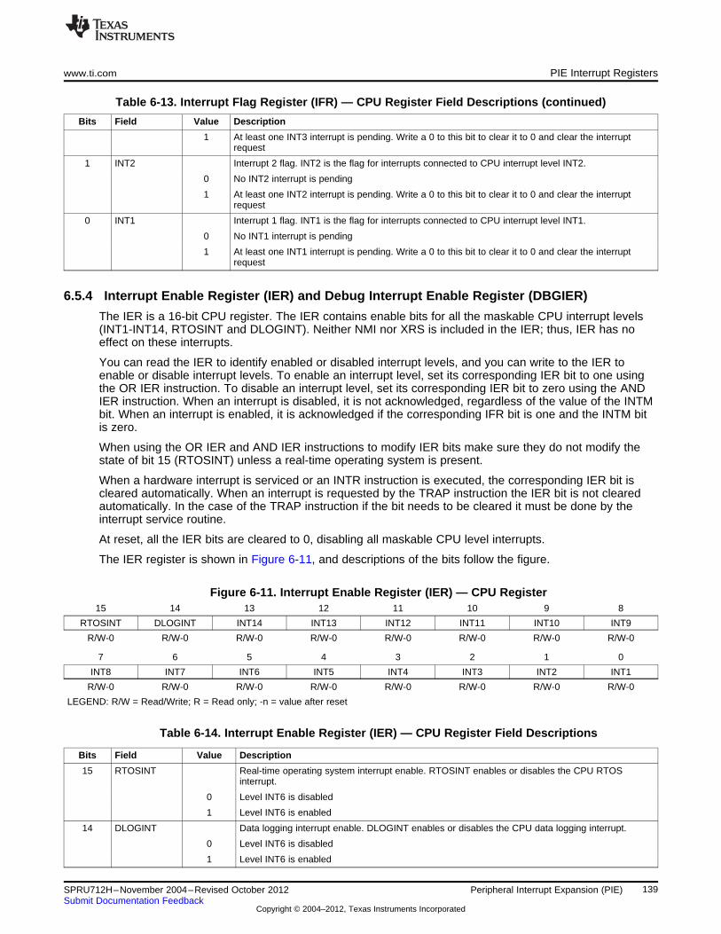
www.ti.com PIE Interrupt Registers
Table 6-13. Interrupt Flag Register (IFR) — CPU Register Field Descriptions (continued)
Bits Field Value Description
1 At least one INT3 interrupt is pending. Write a 0 to this bit to clear it to 0 and clear the interruptrequest
1 INT2 Interrupt 2 flag. INT2 is the flag for interrupts connected to CPU interrupt level INT2.
0 No INT2 interrupt is pending
1 At least one INT2 interrupt is pending. Write a 0 to this bit to clear it to 0 and clear the interruptrequest
0 INT1 Interrupt 1 flag. INT1 is the flag for interrupts connected to CPU interrupt level INT1.
0 No INT1 interrupt is pending
1 At least one INT1 interrupt is pending. Write a 0 to this bit to clear it to 0 and clear the interruptrequest
6.5.4 Interrupt Enable Register (IER) and Debug Interrupt Enable Register (DBGIER)
The IER is a 16-bit CPU register. The IER contains enable bits for all the maskable CPU interrupt levels(INT1-INT14, RTOSINT and DLOGINT). Neither NMI nor XRS is included in the IER; thus, IER has noeffect on these interrupts.
You can read the IER to identify enabled or disabled interrupt levels, and you can write to the IER toenable or disable interrupt levels. To enable an interrupt level, set its corresponding IER bit to one usingthe OR IER instruction. To disable an interrupt level, set its corresponding IER bit to zero using the ANDIER instruction. When an interrupt is disabled, it is not acknowledged, regardless of the value of the INTMbit. When an interrupt is enabled, it is acknowledged if the corresponding IFR bit is one and the INTM bitis zero.
When using the OR IER and AND IER instructions to modify IER bits make sure they do not modify thestate of bit 15 (RTOSINT) unless a real-time operating system is present.
When a hardware interrupt is serviced or an INTR instruction is executed, the corresponding IER bit iscleared automatically. When an interrupt is requested by the TRAP instruction the IER bit is not clearedautomatically. In the case of the TRAP instruction if the bit needs to be cleared it must be done by theinterrupt service routine.
At reset, all the IER bits are cleared to 0, disabling all maskable CPU level interrupts.
The IER register is shown in Figure 6-11, and descriptions of the bits follow the figure.
Figure 6-11. Interrupt Enable Register (IER) — CPU Register15 14 13 12 11 10 9 8
RTOSINT DLOGINT INT14 INT13 INT12 INT11 INT10 INT9
R/W-0 R/W-0 R/W-0 R/W-0 R/W-0 R/W-0 R/W-0 R/W-0
7 6 5 4 3 2 1 0
INT8 INT7 INT6 INT5 INT4 INT3 INT2 INT1
R/W-0 R/W-0 R/W-0 R/W-0 R/W-0 R/W-0 R/W-0 R/W-0
LEGEND: R/W = Read/Write; R = Read only; -n = value after reset
Table 6-14. Interrupt Enable Register (IER) — CPU Register Field Descriptions
Bits Field Value Description
15 RTOSINT Real-time operating system interrupt enable. RTOSINT enables or disables the CPU RTOSinterrupt.
0 Level INT6 is disabled
1 Level INT6 is enabled
14 DLOGINT Data logging interrupt enable. DLOGINT enables or disables the CPU data logging interrupt.
0 Level INT6 is disabled
1 Level INT6 is enabled
139SPRU712H–November 2004–Revised October 2012 Peripheral Interrupt Expansion (PIE)Submit Documentation Feedback
Copyright © 2004–2012, Texas Instruments Incorporated

PIE Interrupt Registers www.ti.com
Table 6-14. Interrupt Enable Register (IER) — CPU Register Field Descriptions (continued)
Bits Field Value Description
13 INT14 Interrupt 14 enable. INT14 enables or disables CPU interrupt level INT14.
0 Level INT14 is disabled
1 Level INT14 is enabled
12 INT13 Interrupt 13 enable. INT13 enables or disables CPU interrupt level INT13.
0 Level INT13 is disabled
1 Level INT13 is enabled
11 INT12 Interrupt 12 enable. INT12 enables or disables CPU interrupt level INT12.
0 Level INT12 is disabled
1 Level INT12 is enabled
10 INT11 Interrupt 11 enable. INT11 enables or disables CPU interrupt level INT11.
0 Level INT11 is disabled
1 Level INT11 is enabled
9 INT10 Interrupt 10 enable. INT10 enables or disables CPU interrupt level INT10.
0 Level INT10 is disabled
1 Level INT10 is enabled
8 INT9 Interrupt 9 enable. INT9 enables or disables CPU interrupt level INT9.
0 Level INT9 is disabled
1 Level INT9 is enabled
7 INT8 Interrupt 8 enable. INT8 enables or disables CPU interrupt level INT8.
0 Level INT8 is disabled
1 Level INT8 is enabled
6 INT7 Interrupt 7 enable. INT7 enables or disables CPU interrupt level INT7.
0 Level INT7 is disabled
1 Level INT7 is enabled
5 INT6 Interrupt 6 enable. INT6 enables or disables CPU interrupt level INT6.
0 Level INT6 is disabled
1 Level INT6 is enabled
4 INT5 Interrupt 5 enable.INT5 enables or disables CPU interrupt level INT5.
0 Level INT5 is disabled
1 Level INT5 is enabled
3 INT4 Interrupt 4 enable.INT4 enables or disables CPU interrupt level INT4.
0 Level INT4 is disabled
1 Level INT4 is enabled
2 INT3 Interrupt 3 enable.INT3 enables or disables CPU interrupt level INT3.
0 Level INT3 is disabled
1 Level INT3 is enabled
1 INT2 Interrupt 2 enable.INT2 enables or disables CPU interrupt level INT2.
0 Level INT2 is disabled
1 Level INT2 is enabled
0 INT1 Interrupt 1 enable.INT1 enables or disables CPU interrupt level INT1.
0 Level INT1 is disabled
1 Level INT1 is enabled
The Debug Interrupt Enable Register (DBGIER) is used only when the CPU is halted in real-timeemulation mode. An interrupt enabled in the DBGIER is defined as a time-critical interrupt. When the CPUis halted in real-time mode, the only interrupts that are serviced are time-critical interrupts that are alsoenabled in the IER. If the CPU is running in real-time emulation mode, the standard interrupt-handlingprocess is used and the DBGIER is ignored.
140 Peripheral Interrupt Expansion (PIE) SPRU712H–November 2004–Revised October 2012Submit Documentation Feedback
Copyright © 2004–2012, Texas Instruments Incorporated
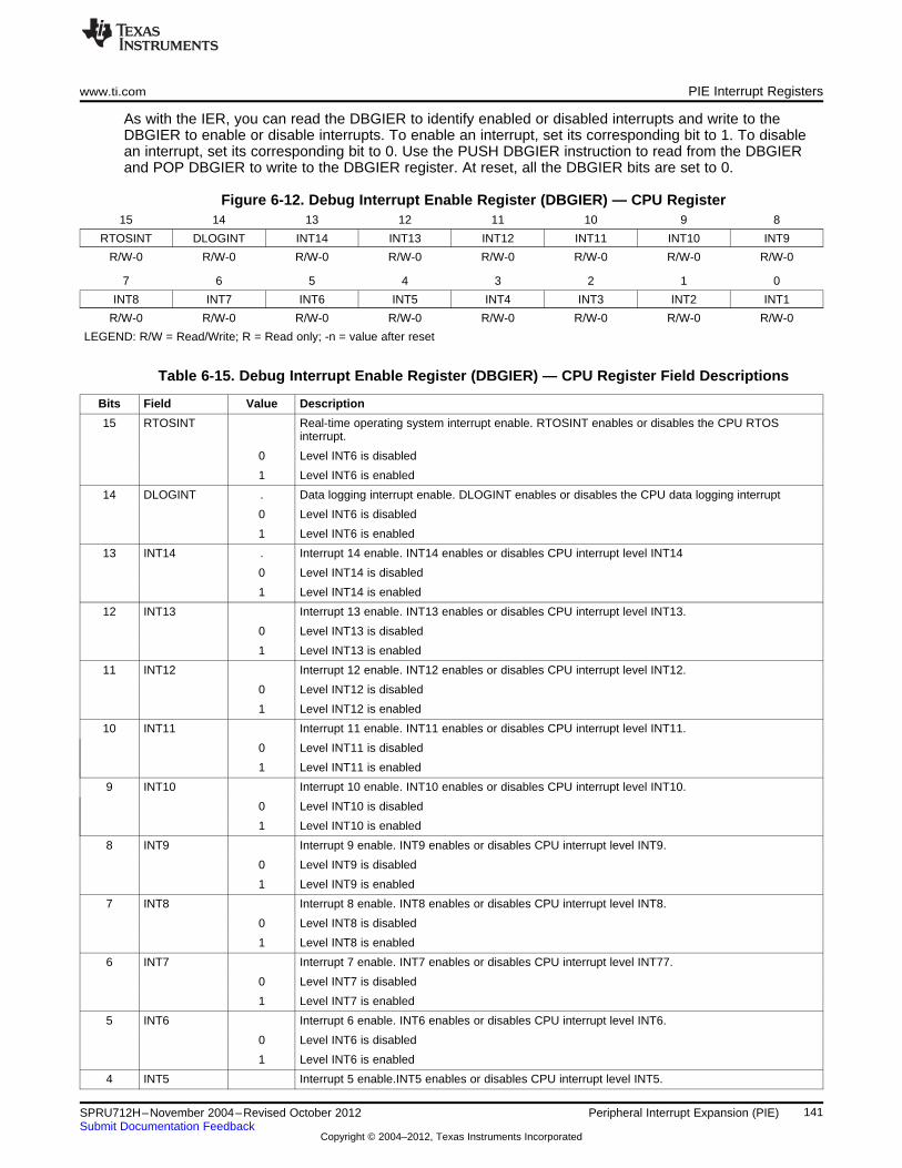
www.ti.com PIE Interrupt Registers
As with the IER, you can read the DBGIER to identify enabled or disabled interrupts and write to theDBGIER to enable or disable interrupts. To enable an interrupt, set its corresponding bit to 1. To disablean interrupt, set its corresponding bit to 0. Use the PUSH DBGIER instruction to read from the DBGIERand POP DBGIER to write to the DBGIER register. At reset, all the DBGIER bits are set to 0.
Figure 6-12. Debug Interrupt Enable Register (DBGIER) — CPU Register15 14 13 12 11 10 9 8
RTOSINT DLOGINT INT14 INT13 INT12 INT11 INT10 INT9
R/W-0 R/W-0 R/W-0 R/W-0 R/W-0 R/W-0 R/W-0 R/W-0
7 6 5 4 3 2 1 0
INT8 INT7 INT6 INT5 INT4 INT3 INT2 INT1
R/W-0 R/W-0 R/W-0 R/W-0 R/W-0 R/W-0 R/W-0 R/W-0
LEGEND: R/W = Read/Write; R = Read only; -n = value after reset
Table 6-15. Debug Interrupt Enable Register (DBGIER) — CPU Register Field Descriptions
Bits Field Value Description
15 RTOSINT Real-time operating system interrupt enable. RTOSINT enables or disables the CPU RTOSinterrupt.
0 Level INT6 is disabled
1 Level INT6 is enabled
14 DLOGINT . Data logging interrupt enable. DLOGINT enables or disables the CPU data logging interrupt
0 Level INT6 is disabled
1 Level INT6 is enabled
13 INT14 . Interrupt 14 enable. INT14 enables or disables CPU interrupt level INT14
0 Level INT14 is disabled
1 Level INT14 is enabled
12 INT13 Interrupt 13 enable. INT13 enables or disables CPU interrupt level INT13.
0 Level INT13 is disabled
1 Level INT13 is enabled
11 INT12 Interrupt 12 enable. INT12 enables or disables CPU interrupt level INT12.
0 Level INT12 is disabled
1 Level INT12 is enabled
10 INT11 Interrupt 11 enable. INT11 enables or disables CPU interrupt level INT11.
0 Level INT11 is disabled
1 Level INT11 is enabled
9 INT10 Interrupt 10 enable. INT10 enables or disables CPU interrupt level INT10.
0 Level INT10 is disabled
1 Level INT10 is enabled
8 INT9 Interrupt 9 enable. INT9 enables or disables CPU interrupt level INT9.
0 Level INT9 is disabled
1 Level INT9 is enabled
7 INT8 Interrupt 8 enable. INT8 enables or disables CPU interrupt level INT8.
0 Level INT8 is disabled
1 Level INT8 is enabled
6 INT7 Interrupt 7 enable. INT7 enables or disables CPU interrupt level INT77.
0 Level INT7 is disabled
1 Level INT7 is enabled
5 INT6 Interrupt 6 enable. INT6 enables or disables CPU interrupt level INT6.
0 Level INT6 is disabled
1 Level INT6 is enabled
4 INT5 Interrupt 5 enable.INT5 enables or disables CPU interrupt level INT5.
141SPRU712H–November 2004–Revised October 2012 Peripheral Interrupt Expansion (PIE)Submit Documentation Feedback
Copyright © 2004–2012, Texas Instruments Incorporated

External Interrupt Control Registers www.ti.com
Table 6-15. Debug Interrupt Enable Register (DBGIER) — CPU Register Field Descriptions (continued)
Bits Field Value Description
0 Level INT5 is disabled
1 Level INT5 is enabled
3 INT4 Interrupt 4 enable.INT4 enables or disables CPU interrupt level INT4.
0 Level INT4 is disabled
1 Level INT4 is enabled
2 INT3 Interrupt 3 enable.INT3 enables or disables CPU interrupt level INT3.
0 Level INT3 is disabled
1 Level INT3 is enabled
1 INT2 Interrupt 2 enable.INT2 enables or disables CPU interrupt level INT2.
0 Level INT2 is disabled
1 Level INT2 is enabled
0 INT1 Interrupt 1 enable.INT1 enables or disables CPU interrupt level INT1.
0 Level INT1 is disabled
1 Level INT1 is enabled
6.6 External Interrupt Control Registers
Some devices support three masked external interrupts XINT1, XINT2, XINT13. XINT13 is multiplexedwith one non-maskable interrupt XNMI. Each of these external interrupts can be selected for negative orpositive edge triggered and can also be enabled or disabled (including XNMI). The masked interrupts alsocontain a 16-bit free running up counter that is reset to zero when a valid interrupt edge is detected. Thiscounter can be used to accurately time stamp the interrupt.
Figure 6-13. External Interrupt 1 Control Register (XINT1CR) (Address 7070h)15 4 3 2 1 0
Reserved Polarity Reserved Enable
R-0 R/W-0 R-0 R/W-0
LEGEND: R/W = Read/Write; R = Read only; -n = value after reset
Table 6-16. External Interrupt 1 Control Register (XINT1CR) Field Descriptions
Bits Field Value Description
15-4 Reserved Reads return zero; writes have no effect.
3-2 Polarity This read/write bit determines whether interrupts are generated on the rising edge or the falling edgeof a signal on the pin.
00 Interrupt generated on a falling edge (high-to-low transition)
01 Interrupt generated on a rising edge (low-to-high transition)
10 Interrupt generated on a falling edge (high-to-low transition)
11 Interrupt generated on both a falling edge and a rising edge (high-to-low transition and low-to-hightransition)
1 Reserved Reads return zero; writes have no effect
0 Enable This read/write bit enables or disables external interrupt XINT1.
0 Disable interrupt
1 Enable interrupt
Figure 6-14. External Interrupt 2 Control Register (XINT2CR) (Address 7071h)15 4 3 2 1 0
Reserved Polarity Reserved Enable
R-0 R/W-0 R-0 R/W-0
LEGEND: R/W = Read/Write; R = Read only; -n = value after reset
142 Peripheral Interrupt Expansion (PIE) SPRU712H–November 2004–Revised October 2012Submit Documentation Feedback
Copyright © 2004–2012, Texas Instruments Incorporated

www.ti.com External Interrupt Control Registers
Table 6-17. External Interrupt 2 Control Register (XINT2CR) Field Descriptions
Bits Field Value Description
15-4 Reserved Reads return zero; writes have no effect.
3-2 Polarity This read/write bit determines whether interrupts are generated on the rising edge or thefalling edge of a signal on the pin.
00 Interrupt generated on a falling edge (high-to-low transition)
01 Interrupt generated on a rising edge (low-to-high transition)
10 Interrupt is generated on a falling edge (high-to-low transition)
11 Interrupt generated on both a falling edge and a rising edge (high-to-low and low-to-hightransition)
1 Reserved Reads return zero; writes have no effect
0 Enable This read/write bit enables or disables external interrupt XINT2.
0 Disable interrupt
1 Enable interrupt
Figure 6-15. External NMI Interrupt Control Register (XNMICR) — Address 7077h15 4 3 2 1 0
Reserved Polarity Select Enable
R-0 R/W-0 R-0 R/W-0
LEGEND: R/W = Read/Write; R = Read only; -n = value after reset
Table 6-18. External NMI Interrupt Control Register (XNMICR) Field Descriptions
Bits Field Value Description
15-4 Reserved Reads return zero; writes have no effect.
3-2 Polarity This read/write bit determines whether interrupts are generated on the rising edge or thefalling edge of the signal on the pin.
00 Interrupt generated on a falling edge (high-to-low transition)
01 Interrupt generated on a rising edge low-to-high transition)
10 Interrupt is generated on a falling edge (high to low transition)
11 Interrupt generated on both a falling edge and a rising edge (high to low and low to hightransition)
1 Select Select the source for INT13
0 Timer 1 connected To INT13
1 XNMI_XINT13 connected To INT13
0 Enable This read/write bit enables or disables external interrupt NMI
0 Disable XNMI interrupt
1 Enable XNMI interrupt
The XNMI Control Register (XNMICR) can be used to enable or disable the NMI interrupt to the CPU. Inaddition, you can select the source for the INT13 CPU interrupt. As shown in Figure 6-4, the source of theINT13 interrupt can be either the internal CPU Timer1 or the external GPIO signal assigned to XNMI.
Table 6-19. XNMICR Register Settings and Interrupt Sources
XNMICR Register Bits 28x CPU Interrupt Timestamp
ENABLE SELECT NMI Source INT13 Source (XNMICTR)
0 0 Disabled CPU Timer 1 None
0 1 Disabled XNMI None
1 0 XNMI CPU Timer 1 XNMI
1 1 Disabled XNMI XNMI
143SPRU712H–November 2004–Revised October 2012 Peripheral Interrupt Expansion (PIE)Submit Documentation Feedback
Copyright © 2004–2012, Texas Instruments Incorporated
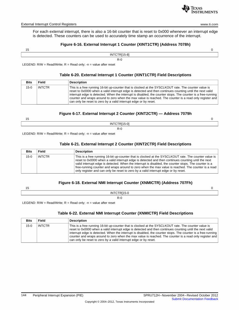
External Interrupt Control Registers www.ti.com
For each external interrupt, there is also a 16-bit counter that is reset to 0x000 whenever an interrupt edgeis detected. These counters can be used to accurately time stamp an occurrence of the interrupt.
Figure 6-16. External Interrupt 1 Counter (XINT1CTR) (Address 7078h)15 0
INTCTR[15-8]
R-0
LEGEND: R/W = Read/Write; R = Read only; -n = value after reset
Table 6-20. External Interrupt 1 Counter (XINT1CTR) Field Descriptions
Bits Field Description
15-0 INTCTR This is a free running 16-bit up-counter that is clocked at the SYSCLKOUT rate. The counter value isreset to 0x0000 when a valid interrupt edge is detected and then continues counting until the next validinterrupt edge is detected. When the interrupt is disabled, the counter stops. The counter is a free-runningcounter and wraps around to zero when the max value is reached. The counter is a read only register andcan only be reset to zero by a valid interrupt edge or by reset.
Figure 6-17. External Interrupt 2 Counter (XINT2CTR) — Address 7079h15 0
INTCTR[15-0]
R-0
LEGEND: R/W = Read/Write; R = Read only; -n = value after reset
Table 6-21. External Interrupt 2 Counter (XINT2CTR) Field Descriptions
Bits Field Description
15-0 INTCTR This is a free running 16-bit up-counter that is clocked at the SYSCLKOUT rate. The counter value isreset to 0x0000 when a valid interrupt edge is detected and then continues counting until the nextvalid interrupt edge is detected. When the interrupt is disabled, the counter stops. The counter is afree-running counter and wraps around to zero when the max value is reached. The counter is a readonly register and can only be reset to zero by a valid interrupt edge or by reset.
Figure 6-18. External NMI Interrupt Counter (XNMICTR) (Address 707Fh)15 0
INTCTR[15-0
R-0
LEGEND: R/W = Read/Write; R = Read only; -n = value after reset
Table 6-22. External NMI Interrupt Counter (XNMICTR) Field Descriptions
Bits Field Description
15-0 INTCTR This is a free running 16-bit up-counter that is clocked at the SYSCLKOUT rate. The counter value isreset to 0x0000 when a valid interrupt edge is detected and then continues counting until the next validinterrupt edge is detected. When the interrupt is disabled, the counter stops. The counter is a free-runningcounter and wraps around to zero when the max value is reached. The counter is a read only register andcan only be reset to zero by a valid interrupt edge or by reset.
144 Peripheral Interrupt Expansion (PIE) SPRU712H–November 2004–Revised October 2012Submit Documentation Feedback
Copyright © 2004–2012, Texas Instruments Incorporated

Appendix ASPRU712H–November 2004–Revised October 2012
Submitting ROM Codes to TI
This appendix defines the scope of code-customized DSPs and describes the procedures for developingprototype and production units. Information on submitting object code and on ordering customer ROM-coded devices is also included.
Topic ........................................................................................................................... Page
A.1 Scope ............................................................................................................. 146A.2 Procedure ....................................................................................................... 146A.3 Code Submittal ................................................................................................ 148A.4 Ordering ......................................................................................................... 148
145SPRU712H–November 2004–Revised October 2012 Submitting ROM Codes to TISubmit Documentation Feedback
Copyright © 2004–2012, Texas Instruments Incorporated

Scope www.ti.com
A.1 Scope
Code-customized DSP processors with on-chip ROM offer the advantage of lower system cost for volume-driven applications.
A repetitive routine (for example, boot code) or an entire system algorithm can be embedded(programmed) into the on-chip ROM of a TMS320 DSP.
The embedded device, due to its customer-specific code, can only be offered for sale as such to thatcustomer or the customer’s formally designated representative. The customer’s intellectual property withinthe device is protected by a unique part number, as well as the on-chip code security module.
Standard TMS320 development tools are used to develop, test, refine, and finalize the application code.Code development can be done using the on-chip flash memory and/or external RAM (if applicable).When the code has been finalized, you may submit to Texas Instruments for masking into the on-chipprogram ROM.
A.2 Procedure
Figure A-1 illustrates the procedural flow for TMS320 masked parts. When ordering, there is a one-timenonrefundable (NRE) charge for mask tooling and related one-time engineering costs. This charge alsocovers the costs for a finite number of supplied prototype units. A minimum production order per year isrequired for any masked-ROM device, and assurance of that order is expected at the time of NRE orderacceptance.
146 Submitting ROM Codes to TI SPRU712H–November 2004–Revised October 2012Submit Documentation Feedback
Copyright © 2004–2012, Texas Instruments Incorporated

Customer submitscustom code
Customer submitsdevice requirements
Customer submits newcode release form
TI performsROM receipt
CustomerApproves
ROM receipt
No
TI orders masks,manufactures, andships prototypes
Yes
Customerapprovesprototype
No
Yes
Customer releasesto production
TI shipsproduction devices
www.ti.com Procedure
Figure A-1. TMS320 ROM Code Prototype and Production Flowchart
A.2.1 Customer Required Information
For TI to accept the receipt of a customer ROM algorithm, each of the following three items must bereceived by the TI factory.
1. The customer completes and submits a New Code Release Form (NCRF— available from TI FieldSales Office) describing the custom features of the device (for example, customer information,prototype and production quantities and dates, any exceptions to standard electrical specifications,customer part numbers, and symbolization, package type, etc.).
2. If nonstandard specifications are requested on the NCRF, the customer submits a copy of thespecification for the DSP in the customer’s system, including functional description and electricalspecification (including absolute maximum ratings, recommended operating conditions, and timingvalues).
3. When the customer has completed code development and has verified this code with the developmentsystem, the standard TMS320 COFF file is submitted to the TI factory via email.
The completed NCRF, customer specification (if required), and ROM code should be given to the TI FieldSales Office.
147SPRU712H–November 2004–Revised October 2012 Submitting ROM Codes to TISubmit Documentation Feedback
Copyright © 2004–2012, Texas Instruments Incorporated

Code Submittal www.ti.com
A.2.2 TI Performs ROM Receipt
Code review and ROM receipt is performed on the customer’s code and a unique manufacturing ROMcode number (such as Dxxxxx) is assigned to the customer’s algorithm. All future correspondence shouldindicate this number. The ROM receipt procedure reads the ROM code information, processes it, andreturns the processed and the original code to the customer for verification of correct ROM receipt.
A.2.3 Customer Approves ROM Receipt
The customer then verifies that the ROM code received and processed by TI is correct and that noinformation was misinterpreted in the transfer. The customer must then return written confirmation ofcorrect ROM receipt verification or resubmit the code for processing. This written confirmation ofverification constitutes the contractual agreement for creation of the custom mask and manufacture ofROM verification prototype units.
A.2.4 TI Orders Masks, Manufactures, and Ships Prototypes
TI generates the prototype photomasks, processes, manufactures, and tests device prototypes containingthe customer’s ROM pattern for shipment to the customer for ROM code verification. These devices havebeen made using the custom mask but are for the purposes of ROM verification only. For expediency, theprototype devices are tested only at room temperatures (25°C). Texas Instruments recommends thatprototype devices not be used in production systems.
A.2.5 Customer Approves Prototype
The customer verifies the operation of these prototypes in the system and responds with written customerprototype approval or disapproval. This written customer prototype approval constitutes the contractualagreement to initiate volume production using the verified prototype ROM code.
A.2.6 Customer Release to Production
With customer approval, the ROM code is released to production and TI begins shipment of productiondevices according to the customer’s final specifications and order requirements.
Two lead times are quoted in reference to the preceding flow:
• Prototype lead time is the elapsed time from the receipt of written ROM receipt verification to thedelivery of the prototype devices.
• Production lead time is the elapsed time from the receipt of written customer prototype approval tothe delivery of production devices. For the latest TMS320 family lead times, contact the nearest TIField Sales Office.
A.3 Code Submittal
The customer’s object code (in COFF format) can be submitted via electronic transmittal.
When a code is submitted to Texas Instruments for masking, the code is reformatted by TI toaccommodate the TI mask-making and test program generation systems. Application-level verification bythe customer is, therefore, necessary. Although the code has been reformatted, it is important that thechanges remain transparent to the user and do not affect the execution of the algorithm submitted. Thoseformatting changes consist essentially of adding ease-of-manufacturing code in reserved and not used(customer) locations only. Resulting code has the code address beginning at the base address of theROM in the TMS320 device and progressing without gaps to the last address of the ROM on the TMS320device. Note that because these changes have been made, a checksum comparison is not a valid meansof verification. Upon satisfactory verification of the TI returned code, the customer advises TI in writing thatit is verified, and this enables release to manufacturing and acceptance of initial orders.
A.4 Ordering
Customer embedded-code devices are user-specified, and thus, each is an unreleased new product untilprototype approval and formal release to production. With each initial order of a ROM-coded device, thecustomer must include written recognition that he understands the following:
148 Submitting ROM Codes to TI SPRU712H–November 2004–Revised October 2012Submit Documentation Feedback
Copyright © 2004–2012, Texas Instruments Incorporated

www.ti.com Ordering
The units to be shipped against this order were assembled, for expediency purposes, on aprototype (that is, nonproduction qualified) manufacturing line, the reliability of which is not fullycharacterized. Therefore, the anticipated reliability of these prototype units cannot be defined.
Sometimes to shorten time to market and upon mutual agreement, the customer may order (and TI willaccept) a Risk Production order prior to prototype approval. Under this noncancellable order arrangement,the customer agrees to accept delivery of product containing his code as initially verified and TI agrees toship to that requirement. The customer is, in effect, agreeing to not change the originally submitted codefor the Risk Production order units. He must use the term “Risk Production” in a letter or in a note on theorder as a matter of record.
TI does reserve the right to sell excess customer ROM-coded devices as standards to reduce the financialliability incurred through premature ordered quantity reductions or overbuilds. Units thus marketed by TIhave all original customer custom symbols or other means of external identification, removed and replacedby a standard product symbol to mask the custom die presence. It is standard practice to require a one-time statement from the customer stating that the customer knows and concurs.
Your local TI Field Sales Office and/or TI Authorized Distributor can be of further assistance on embeddedROM procedure questions and in actually processing your code.
149SPRU712H–November 2004–Revised October 2012 Submitting ROM Codes to TISubmit Documentation Feedback
Copyright © 2004–2012, Texas Instruments Incorporated
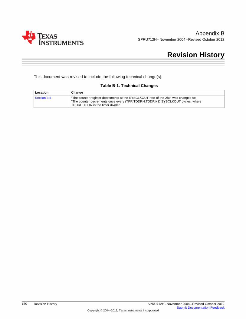
Appendix BSPRU712H–November 2004–Revised October 2012
Revision History
This document was revised to include the following technical change(s).
Table B-1. Technical Changes
Location Change
Section 3.5 “The counter register decrements at the SYSCLKOUT rate of the 28x” was changed to:"The counter decrements once every (TPR[TDDRH:TDDR]+1) SYSCLKOUT cycles, whereTDDRH:TDDR is the timer divider.
150 Revision History SPRU712H–November 2004–Revised October 2012Submit Documentation Feedback
Copyright © 2004–2012, Texas Instruments Incorporated

IMPORTANT NOTICE
Texas Instruments Incorporated and its subsidiaries (TI) reserve the right to make corrections, enhancements, improvements and otherchanges to its semiconductor products and services per JESD46, latest issue, and to discontinue any product or service per JESD48, latestissue. Buyers should obtain the latest relevant information before placing orders and should verify that such information is current andcomplete. All semiconductor products (also referred to herein as “components”) are sold subject to TI’s terms and conditions of salesupplied at the time of order acknowledgment.
TI warrants performance of its components to the specifications applicable at the time of sale, in accordance with the warranty in TI’s termsand conditions of sale of semiconductor products. Testing and other quality control techniques are used to the extent TI deems necessaryto support this warranty. Except where mandated by applicable law, testing of all parameters of each component is not necessarilyperformed.
TI assumes no liability for applications assistance or the design of Buyers’ products. Buyers are responsible for their products andapplications using TI components. To minimize the risks associated with Buyers’ products and applications, Buyers should provideadequate design and operating safeguards.
TI does not warrant or represent that any license, either express or implied, is granted under any patent right, copyright, mask work right, orother intellectual property right relating to any combination, machine, or process in which TI components or services are used. Informationpublished by TI regarding third-party products or services does not constitute a license to use such products or services or a warranty orendorsement thereof. Use of such information may require a license from a third party under the patents or other intellectual property of thethird party, or a license from TI under the patents or other intellectual property of TI.
Reproduction of significant portions of TI information in TI data books or data sheets is permissible only if reproduction is without alterationand is accompanied by all associated warranties, conditions, limitations, and notices. TI is not responsible or liable for such altereddocumentation. Information of third parties may be subject to additional restrictions.
Resale of TI components or services with statements different from or beyond the parameters stated by TI for that component or servicevoids all express and any implied warranties for the associated TI component or service and is an unfair and deceptive business practice.TI is not responsible or liable for any such statements.
Buyer acknowledges and agrees that it is solely responsible for compliance with all legal, regulatory and safety-related requirementsconcerning its products, and any use of TI components in its applications, notwithstanding any applications-related information or supportthat may be provided by TI. Buyer represents and agrees that it has all the necessary expertise to create and implement safeguards whichanticipate dangerous consequences of failures, monitor failures and their consequences, lessen the likelihood of failures that might causeharm and take appropriate remedial actions. Buyer will fully indemnify TI and its representatives against any damages arising out of the useof any TI components in safety-critical applications.
In some cases, TI components may be promoted specifically to facilitate safety-related applications. With such components, TI’s goal is tohelp enable customers to design and create their own end-product solutions that meet applicable functional safety standards andrequirements. Nonetheless, such components are subject to these terms.
No TI components are authorized for use in FDA Class III (or similar life-critical medical equipment) unless authorized officers of the partieshave executed a special agreement specifically governing such use.
Only those TI components which TI has specifically designated as military grade or “enhanced plastic” are designed and intended for use inmilitary/aerospace applications or environments. Buyer acknowledges and agrees that any military or aerospace use of TI componentswhich have not been so designated is solely at the Buyer's risk, and that Buyer is solely responsible for compliance with all legal andregulatory requirements in connection with such use.
TI has specifically designated certain components which meet ISO/TS16949 requirements, mainly for automotive use. Components whichhave not been so designated are neither designed nor intended for automotive use; and TI will not be responsible for any failure of suchcomponents to meet such requirements.
Products Applications
Audio www.ti.com/audio Automotive and Transportation www.ti.com/automotive
Amplifiers amplifier.ti.com Communications and Telecom www.ti.com/communications
Data Converters dataconverter.ti.com Computers and Peripherals www.ti.com/computers
DLP® Products www.dlp.com Consumer Electronics www.ti.com/consumer-apps
DSP dsp.ti.com Energy and Lighting www.ti.com/energy
Clocks and Timers www.ti.com/clocks Industrial www.ti.com/industrial
Interface interface.ti.com Medical www.ti.com/medical
Logic logic.ti.com Security www.ti.com/security
Power Mgmt power.ti.com Space, Avionics and Defense www.ti.com/space-avionics-defense
Microcontrollers microcontroller.ti.com Video and Imaging www.ti.com/video
RFID www.ti-rfid.com
OMAP Applications Processors www.ti.com/omap TI E2E Community e2e.ti.com
Wireless Connectivity www.ti.com/wirelessconnectivity
Mailing Address: Texas Instruments, Post Office Box 655303, Dallas, Texas 75265Copyright © 2012, Texas Instruments Incorporated