TMS320x280x, 2801x, 2804x DSP Analog-to-DigitalConverter · PDF fileTMS320x280x, 2801x, 2804x...
46
TMS320x280x, 2801x, 2804x DSP Analog-to-Digital Converter (ADC) Reference Guide Literature Number: SPRU716D November 2004– Revised April 2010
Transcript of TMS320x280x, 2801x, 2804x DSP Analog-to-DigitalConverter · PDF fileTMS320x280x, 2801x, 2804x...

TMS320x280x, 2801x, 2804x DSPAnalog-to-Digital Converter (ADC)
Reference Guide
Literature Number: SPRU716D
November 2004–Revised April 2010

2 SPRU716D–November 2004–Revised April 2010
Copyright © 2004–2010, Texas Instruments Incorporated

Contents
Preface ....................................................................................................................................... 7
1 Analog-to-Digital Converter (ADC) ....................................................................................... 111.1 Features .................................................................................................................... 121.2 Autoconversion Sequencer Principle of Operation .................................................................... 14
1.2.1 Sequential Sampling Mode ...................................................................................... 151.2.2 Simultaneous Sampling Mode .................................................................................. 15
1.3 Uninterrupted Autosequenced Mode ................................................................................... 211.3.1 Sequencer Start/Stop Mode (Sequencer Start/Stop Operation With Multiple Time-Sequenced
Triggers) ........................................................................................................... 231.3.2 Simultaneous Sampling Mode .................................................................................. 251.3.3 Input Trigger Description ........................................................................................ 251.3.4 Interrupt Operation During Sequenced Conversions ........................................................ 26
1.4 ADC Clock Prescaler ...................................................................................................... 281.4.1 ADC-module Clock and Sample Rate ......................................................................... 28
1.5 Low-power Modes ......................................................................................................... 281.6 Power-up Sequence ...................................................................................................... 281.7 Sequencer Override Feature ............................................................................................. 291.8 Internal/External Reference Voltage Selection ........................................................................ 301.9 Offset Error Correction .................................................................................................... 31
2 ADC Registers .................................................................................................................. 332.1 ADC Control Registers .................................................................................................... 342.2 Maximum Conversion Channels Register (ADCMAXCONV) ........................................................ 382.3 Autosequence Status Register (ADCASEQSR) ....................................................................... 402.4 ADC Status and Flag Register (ADCST) ............................................................................... 412.5 ADC Reference Select Register (ADCREFSEL) ...................................................................... 422.6 ADC Offset Trim Register (ADCOFFTRIM) ............................................................................ 422.7 ADC Input Channel Select Sequencing Control Registers ........................................................... 432.8 ADC Conversion Result Buffer Registers (ADCRESULTn) .......................................................... 44
A Revision History ................................................................................................................ 45
3SPRU716D–November 2004–Revised April 2010 Contents
Copyright © 2004–2010, Texas Instruments Incorporated

www.ti.com
List of Figures
1-1. Block Diagram of the ADC Module...................................................................................... 13
1-2. Sequential Sampling Mode (SMODE = 0) ............................................................................. 15
1-3. Simultaneous Sampling Mode (SMODE=1) ........................................................................... 16
1-4. Block Diagram of Autosequenced ADC in Cascaded Mode ........................................................ 17
1-5. Block Diagram of Autosequenced ADC With Dual Sequencers .................................................... 18
1-6. Flow Chart for Uninterrupted Autosequenced Mode.................................................................. 23
1-7. Example of ePWM Triggers to Start the Sequencer ................................................................. 24
1-8. Interrupt Operation During Sequenced Conversions ................................................................ 27
1-9. ADC Core Clock and Sample-and-Hold (S/H) Clock ................................................................. 28
1-10. Clock Chain to the ADC .................................................................................................. 28
1-11. External Bias for 2.048-V External Reference ......................................................................... 30
1-12. Flow Chart of Offset Error Correction Process ........................................................................ 31
1-13. Ideal Code Distribution of Sampled 0-V Reference................................................................... 32
2-1. ADC Control Register 1 (ADCTRL1) (Address Offset 00h) .......................................................... 34
2-2. ADC Control Register 2 (ADCTRL2) (Address Offset 01h) .......................................................... 35
2-3. ADC Control Register 3 (ADCTRL3) (Address Offset 18h) .......................................................... 37
2-4. Maximum Conversion Channels Register (ADCMAXCONV) (Offset Address 02h) ............................. 38
2-5. Autosequence Status Register (ADCASEQSR) (Address Offset 07h) ............................................. 40
2-6. ADC Status and Flag Register (ADCST) (Address Offset 19h) ..................................................... 41
2-7. ADC Reference Select Register (ADCREFSEL) (Address Offset 1Ch)............................................ 42
2-8. ADC Offset Trim Register (ADCOFFTRIM) (Address Offset 1Dh).................................................. 42
2-9. ADC Input Channel Select Sequencing Control Registers (ADCCHSELSEQ1) (Address Offset 03h) ........ 43
2-10. ADC Input Channel Select Sequencing Control Registers (ADCCHSELSEQ2) (Address Offset 04h) ........ 43
2-11. ADC Input Channel Select Sequencing Control Registers (ADCCHSELSEQ3) (Address Offset 05h) ........ 43
2-12. ADC Input Channel Select Sequencing Control Registers (ADCCHSELSEQ4) (Address Offset 06h) ........ 43
2-13. ADC Conversion Result Buffer Registers (ADCRESULTn) - (Addresses 0x7108-0x7117) ..................... 44
2-14. ADC Conversion Result Buffer Registers (ADCRESULTn) - (Addresses 0x0B00-0x0B0F) .................... 44
4 List of Figures SPRU716D–November 2004–Revised April 2010
Copyright © 2004–2010, Texas Instruments Incorporated

www.ti.com
List of Tables
1-1. ADC Registers ............................................................................................................. 13
1-2. Comparison of Single and Cascaded Operating Modes ............................................................ 19
1-3. Values for ADCCHSELSEQn Registers (MAX_CONV1 Set to 6) .................................................. 22
1-4. Values for ADCCHSELSEQn (MAX_CONV1 set to 2) ............................................................... 24
1-5. Values After Second Autoconversion Session ........................................................................ 25
1-6. Input Triggers .............................................................................................................. 25
1-7. Power Options ............................................................................................................. 28
2-1. ADC Control Register 1 (ADCTRL1) Field Descriptions ............................................................. 34
2-2. ADC Control Register 2 (ADCTRL2) Field Descriptions ............................................................. 35
2-3. ADC Control Register 3 (ADCTRL3) Field Descriptions ............................................................. 37
2-4. Maximum Conversion Channels Register (ADCMAXCONV) Field Descriptions.................................. 38
2-5. Bit Selections for MAX_CONV1 for Various Number of Conversions ............................................. 38
2-6. Autosequence Status Register (ADCASEQSR) Field Descriptions................................................. 40
2-7. State of Active Sequencer ............................................................................................... 40
2-8. ADC Status and Flag Register (ADCST) Field Descriptions......................................................... 41
2-9. ADC Reference Select Register (ADCREFSEL) Field Descriptions................................................ 42
2-10. ADC Offset Trim Register (ADCOFFTRIM) Field Descriptions...................................................... 42
2-11. CONVnn Bit Values and the ADC Input Channels Selected ........................................................ 43
A-1. Changes in this Revision ................................................................................................. 45
5SPRU716D–November 2004–Revised April 2010 List of Tables
Copyright © 2004–2010, Texas Instruments Incorporated

6 List of Tables SPRU716D–November 2004–Revised April 2010
Copyright © 2004–2010, Texas Instruments Incorporated

PrefaceSPRU716D–November 2004–Revised April 2010
Read This First
About This Manual
This document describes the features and operation of the analog-to-digital converter (ADC) that isavailable on the TMS320x280x, 2801x, and 2804x digital signal processors (DSPs).
Notational Conventions
This document uses the following conventions.
• The device number TMS320x280x is often abbreviated as 280x.• Hexadecimal numbers are shown with the suffix h. For example, the following number is 40
hexadecimal (decimal 64): 40h. Similarly, binary numbers often are shown with the suffix b. Forexample, the following number is the decimal 4 shown in binary form: 0100b
• Registers in this document are shown in figures and described in tables.
– Each register figure shows a rectangle divided into fields that represent the fields of the register.Each field is labeled with its bit name, its beginning and ending bit numbers above, and itsread/write properties below. A legend explains the notation used for the properties.
– Reserved bits in a register figure designate a bit that cannot be used for applications.• If a signal is active low, it has an overbar. For example, the XRS signal is active low.
Related Documentation From Texas Instruments
The following documents describe the 280x devices and related support tools. Copies of these documentsare available on the Internet at www.ti.com. Tip: Enter the literature number in the search box provided atwww.ti.com.
Data Manuals—SPRS230 — TMS320F2809, F2808, F2806, F2802, F2801, C2802, C2801, and F2801x DSPs Data
Manual contains the pinout, signal descriptions, as well as electrical and timing specifications forthe F280x devices.
SPRZ171 — TMS320F280x, TMS320C280x, and TMS320F2801x DSC Silicon Erratadescribes the advisories and usage notes for different versions of silicon.
SPRS357 — TMS320F28044 Digital Signal Processor Data Manual contains the pinout, signaldescriptions, as well as electrical and timing specifications for the F28044 device.
SPRZ255 — TMS320F28044 DSP Silicon Erratadescribes the advisories and usage notes for different versions of silicon.
CPU User's Guides—SPRU051— TMS320x28xx, 28xxx Serial Communication Interface (SCI) Reference Guide describes the
SCI, which is a two-wire asynchronous serial port, commonly known as a UART. The SCI modulessupport digital communications between the CPU and other asynchronous peripherals that use thestandard non-return-to-zero (NRZ) format.
SPRU059— TMS320x28xx, 28xxx Serial Peripheral Interface (SPI) Reference Guide describes the SPI -a high-speed synchronous serial input/output (I/O) port - that allows a serial bit stream ofprogrammed length (one to sixteen bits) to be shifted into and out of the device at a programmedbit-transfer rate.
7SPRU716D–November 2004–Revised April 2010 Read This First
Copyright © 2004–2010, Texas Instruments Incorporated

Related Documentation From Texas Instruments www.ti.com
SPRU074— TMS320x28xx, 28xxx Enhanced Controller Area Network (eCAN) Reference Guidedescribes the eCAN that uses established protocol to communicate serially with other controllers inelectrically noisy environments.
SPRU430— TMS320C28x DSP CPU and Instruction Set Reference Guide describes the centralprocessing unit (CPU) and the assembly language instructions of the TMS320C28x fixed-pointdigital signal processors (DSPs). It also describes emulation features available on these DSPs.
SPRU513— TMS320C28x Assembly Language Tools User's Guide describes the assembly languagetools (assembler and other tools used to develop assembly language code), assembler directives,macros, common object file format, and symbolic debugging directives for the TMS320C28x device.
SPRU514— TMS320C28x Optimizing C Compiler User's Guide describes the TMS320C28x™ C/C++compiler. This compiler accepts ANSI standard C/C++ source code and produces TMS320 DSPassembly language source code for the TMS320C28x device.
SPRU566— TMS320x28xx, 28xxx Peripheral Reference Guide describes the peripheral reference guidesof the 28x digital signal processors (DSPs).
SPRU608— The TMS320C28x Instruction Set Simulator Technical Overview describes the simulator,available within the Code Composer Studio for TMS320C2000 IDE, that simulates the instructionset of the C28x™ core.
SPRU625— TMS320C28x DSP/BIOS Application Programming Interface (API) Reference Guidedescribes development using DSP/BIOS.
SPRU712— TMS320x28xx, 28xxx System Control and Interrupts Reference Guide describes the variousinterrupts and system control features of the 280x digital signal processors (DSPs).
SPRU721 — TMS320x28xx, 28xxx Inter-Integrated Circuit (I2C) Module Reference Guide describesthe features and operation of the inter-integrated circuit (I2C) module.
SPRU722 — TMS320x280x, 2801x, 2804x Boot ROM Reference Guide describes the purpose andfeatures of the bootloader (factory-programmed boot-loading software). It also describes othercontents of the device on-chip boot ROM and identifies where all of the information is located withinthat memory.
SPRU790 — TMS320x280x, 2801x, 2804x Enhanced Quadrature Encoder Pulse (eQEP) ModuleReference Guide describes the eQEP module, which is used for interfacing with a linear or rotaryincremental encoder to get position, direction, and speed information from a rotating machine inhigh performance motion and position control systems. It includes the module description andregisters
SPRU791— TMS320x28xx, 28xxx Enhanced Pulse Width Modulator (ePWM) Module Reference Guidedescribes the main areas of the enhanced pulse width modulator that include digital motor control,switch mode power supply control, UPS (uninterruptible power supplies), and other forms of powerconversion
SPRU807 — TMS320x280x, 2801x, 2804x Enhanced Capture (eCAP) Module Reference Guidedescribes the enhanced capture module. It includes the module description and registers.
SPRU924 — TMS320x280x, 2801x, 2804x High-Resolution Pulse Width Modulator Reference Guidedescribes the operation of the high-resolution extension to the pulse width modulator (HRPWM).
Application Reports—SPRAA58— TMS320x281x to TMS320x280x Migration Overview describes differences between the
Texas Instruments TMS320x281x and TMS320x280x DSPs to assist in application migration fromthe 281x to the 280x. While the main focus of this document is migration from 281x to 280x, usersconsidering migrating in the reverse direction (280x to 281x) will also find this document useful.
8 Read This First SPRU716D–November 2004–Revised April 2010
Copyright © 2004–2010, Texas Instruments Incorporated

www.ti.com Related Documentation From Texas Instruments
SPRA550— 3.3 V DSP for Digital Motor Control describes a scenario of a 3.3-V-only motor controllerindicating that for most applications, no significant issue of interfacing between 3.3 V and 5 Vexists. On-chip 3.3-V analog-to-digital converter (ADC) versus 5-V ADC is also discussed.Guidelines for component layout and printed circuit board (PCB) design that can reduce systemnoise and EMI effects are summarized.
SPRA820— Online Stack Overflow Detection on the TMS320C28x DSP presents the methodology foronline stack overflow detection on the TMS320C28x™ DSP. C-source code is provided thatcontains functions for implementing the overflow detection on both DSP/BIOS™ andnon-DSP/BIOS applications.
SPRA861— RAMDISK: A Sample User-Defined C I/O Driver provides an easy way to use thesophisticated buffering of the high-level CIO functions on an arbitrary device. This application reportpresents a sample implementation of a user-defined device driver.
SPRA873— Thermo-Electric Cooler Control Using a TMS320F2812 DSP & DRV592 Power Amplifierpresents a thermoelectric cooler system consisting of a Texas Instruments TMS320F2812 digitalsignal processor (DSP) and DRV592 power amplifier. The DSP implements a digitalproportional-integral-derivative feedback controller using an integrated 12-bit analog-to-digitalconverter to read the thermistor, and direct output of pulse-width-modulated waveforms to theH-bridge DRV592 power amplifier. A complete description of the experimental system, along withsoftware and software operating instructions, is provided.
SPRA876— Programming Examples for the TMS320F281x eCAN contains several programmingexamples to illustrate how the eCAN module is set up for different modes of operation to help youcome up to speed quickly in programming the eCAN. All projects and CANalyzer configuration filesare included in the attached SPRA876.zip file.
SPRA953— IC Package Thermal Metrics describes the traditional and new thermal metrics and will puttheir application in perspective with respect to system level junction temperature estimation.
SPRA958— Running an Application from Internal Flash Memory on the TMS320F281x DSP (Rev. B)covers the requirements needed to properly configure application software for execution fromon-chip flash memory. Requirements for both DSP/BIOS™ and non-DSP/BIOS projects arepresented. Example code projects are included.
SPRA963— Reliability Data for TMS320LF24x and TMS320F281x Devices describes reliability data forTMS320LF24x and TMS320F281x devices.
SPRA989— F2810, F2811, and F2812 ADC Calibration describes a method for improving the absoluteaccuracy of the 12-bit analog-to-digital converter (ADC) found on the F2810/F2811/F2812 devices.This application note is accompanied by an example program (ADCcalibration.zip) that executesfrom RAM on the F2812 eZdsp.
SPRA991— Simulation Fulfills its Promise for Enhancing Debug and Analysis - A White Paper describessimulation enhancements that enable developers to speed up the development cycle by allowingthem to evaluate system alternatives more effectively.
TMS320C28x, C28x are trademarks of Texas Instruments.
9SPRU716D–November 2004–Revised April 2010 Read This First
Copyright © 2004–2010, Texas Instruments Incorporated

10 Read This First SPRU716D–November 2004–Revised April 2010
Copyright © 2004–2010, Texas Instruments Incorporated

Chapter 1SPRU716D–November 2004–Revised April 2010
Analog-to-Digital Converter (ADC)
The TMS320x280x ADC module is a 12-bit pipelined analog-to-digital converter (ADC). The analogcircuits of this converter, referred to as the core in this document, include the front-end analog multiplexers(MUXs), sample-and-hold (S/H) circuits, the conversion core, voltage regulators, and other analogsupporting circuits. Digital circuits, referred to as the wrapper in this document, include programmableconversion sequencer, result registers, interface to analog circuits, interface to device peripheral bus, andinterface to other on-chip modules.
This reference guide is applicable for the ADC found on the TMS320x280x family of processors. Thisincludes all Flash-based, ROM-based and RAM-based devices within the 280x family.
Topic ........................................................................................................................... Page
1.1 Features ........................................................................................................... 121.2 Autoconversion Sequencer Principle of Operation ................................................ 141.3 Uninterrupted Autosequenced Mode ................................................................... 211.4 ADC Clock Prescaler ......................................................................................... 281.5 Low-power Modes ............................................................................................. 281.6 Power-up Sequence ........................................................................................... 281.7 Sequencer Override Feature ............................................................................... 291.8 Internal/External Reference Voltage Selection ....................................................... 301.9 Offset Error Correction ...................................................................................... 31
11SPRU716D–November 2004–Revised April 2010 Analog-to-Digital Converter (ADC)
Copyright © 2004–2010, Texas Instruments Incorporated

Digital Value � 0,
Digital Value � 4096 �Input Analog Voltage � ADCLO
3
when input ≤ 0 V
when 0 V < input < 3 V
when input ≥ 3 VDigital Value � 4095,
Features www.ti.com
1.1 Features
The ADC module has 16 channels, configurable as two independent 8-channel modules to service theePWM modules. The two independent 8-channel modules can be cascaded to form a 16-channel module.Although there are multiple input channels and two sequencers, there is only one converter in the ADCmodule. Figure 1-1 shows the block diagram of the ADC module.
The two 8-channel modules can autosequence a series of conversions; each module has the choice ofselecting any one of the respective eight channels available through an analog MUX. In the cascadedmode, the autosequencer functions as a single 16-channel sequencer. On each sequencer, once theconversion is completed, the selected channel value is stored in its respective ADCRESULT register.Autosequencing allows the system to convert the same channel multiple times, allowing the user toperform oversampling algorithms. This oversampling gives increased resolution over traditionalsingle-sampled conversion results.
Functions of the ADC module include:
• 12-bit ADC core with built-in dual sample-and-hold (S/H)• Simultaneous sampling or sequential sampling modes• Analog input: 0 V to 3 V• Fast conversion time runs at 12.5 MHz, ADC clock, or 6.25 MSPS• 16-channel, multiplexed inputs• Autosequencing capability provides up to 16 "autoconversions" in a single session. Each conversion
can be programmed to select any 1 of 16 input channels.• Sequencer can be operated as two independent 8-state sequencers or as one large 16-state
sequencer (i.e., two cascaded 8-state sequencers).• Sixteen result registers (individually addressable) to store conversion values
– The digital value of the input analog voltage is derived by:
A All fractional values are truncated.
• Multiple triggers as sources for the start-of-conversion (SOC) sequence
– S/W - software immediate start– ePWM 1-6– GPIO XINT2
• Flexible interrupt control allows interrupt request on every end-of-sequence (EOS) or every other EOS• Sequencer can operate in "start/stop" mode, allowing multiple "time-sequenced triggers" to
synchronize conversions.• ePWM triggers can operate independently in dual-sequencer mode.• Sample-and-hold (S/H) acquisition time window has separate prescale control.
12 Analog-to-Digital Converter (ADC) SPRU716D–November 2004–Revised April 2010
Copyright © 2004–2010, Texas Instruments Incorporated
Result Registers
ePWMx SOCB
S/W
GPIO/XINT2_
ADCSOC
ePWMx SOCA
S/W
Sequencer 2Sequencer 1 SOCSOC
ADC Control Registers
70B7h
70B0h
70AFh
70A8h
Result Reg 15
Result Reg 8
Result Reg 7
Result Reg 1
Result Reg 0
moduleADC12-Bit
AnalogMUX
ADCINA0
ADCINA7
ADCINB0
ADCINB7
Systemcontrol block
High-speedprescaler
HSPCLK
C28xSYSCLKOUT
S/H-A
S/H-B
ADCENCLK HALT
www.ti.com Features
Figure 1-1. Block Diagram of the ADC Module
Table 1-1. ADC Registers
Name Address (1) Address (2) Size (x16) Description
ADCTRL1 0x7100 1 ADC Control Register 1
ADCTRL2 0x7101 1 ADC Control Register 2
ADCMAXCONV 0x7102 1 ADC Maximum Conversion Channels Register
ADCCHSELSEQ1 0x7103 1 ADC Channel Select Sequencing Control Register 1
ADCCHSELSEQ2 0x7104 1 ADC Channel Select Sequencing Control Register 2
ADCCHSELSEQ3 0x7105 1 ADC Channel Select Sequencing Control Register 3
ADCCHSELSEQ4 0x7106 1 ADC Channel Select Sequencing Control Register 4
ADCASEQSR 0x7107 1 ADC Auto-Sequence Status Register
ADCRESULT0 0x7108 0x0B00 1 ADC Conversion Result Buffer Register 0
ADCRESULT1 0x7109 0x0B01 1 ADC Conversion Result Buffer Register 1
ADCRESULT2 0x710A 0x0B02 1 ADC Conversion Result Buffer Register 2
ADCRESULT3 0x710B 0x0B03 1 ADC Conversion Result Buffer Register 3
ADCRESULT4 0x710C 0x0B04 1 ADC Conversion Result Buffer Register 4
ADCRESULT5 0x710D 0x0B05 1 ADC Conversion Result Buffer Register 5
ADCRESULT6 0x710E 0x0B06 1 ADC Conversion Result Buffer Register 6
ADCRESULT7 0x710F 0x0B07 1 ADC Conversion Result Buffer Register 7
ADCRESULT8 0x7110 0x0B00 1 ADC Conversion Result Buffer Register 8
ADCRESULT9 0x7111 0x0B09 1 ADC Conversion Result Buffer Register 9
(1) The registers in this column are Peripheral Frame 2 registers.(2) The ADC result registers are dual mapped in the device. Locations in Peripheral Frame 2 (0x7108-0x7117) are 2 wait states and
left justified. Locations in Peripheral Frame 0 space (0x0B00-0x0B0F) are 0 wait states and right justified. During highspeed/continuous conversion use of the ADC, use the 0 wait state locations to avoid missing ADC conversions.
13SPRU716D–November 2004–Revised April 2010 Analog-to-Digital Converter (ADC)
Copyright © 2004–2010, Texas Instruments Incorporated

Autoconversion Sequencer Principle of Operation www.ti.com
Table 1-1. ADC Registers (continued)
Name Address (1) Address (2) Size (x16) Description
ADCRESULT10 0x7112 0x0B0A 1 ADC Conversion Result Buffer Register 10
ADCRESULT11 0x7113 0x0B0B 1 ADC Conversion Result Buffer Register 11
ADCRESULT12 0x7114 0x0B0C 1 ADC Conversion Result Buffer Register 12
ADCRESULT13 0x7115 0x0B0D 1 ADC Conversion Result Buffer Register 13
ADCRESULT14 0x7116 0x0B0E 1 ADC Conversion Result Buffer Register 14
ADCRESULT15 0x7117 0x0B0F 1 ADC Conversion Result Buffer Register 15
ADCTRL3 0x7118 1 ADC Control Register 3
ADCST 0x7119 1 ADC Status Register
0x711AReserved 20x711B
ADCREFSEL 0x711C 1 ADC Reference Select Register
ADCOFFTRIM 0x711D 1 ADC Offset Trim Register
0x711EReserved 2 ADC Status Register0x711F
To obtain the specified accuracy of the ADC, proper board layout is very critical. To the best extentpossible, traces leading to the ADCINxx pins should not run in close proximity to the digital signal paths.This is to minimize switching noise on the digital lines from getting coupled to the ADC inputs.Furthermore, proper isolation techniques must be used to isolate the ADC module power pins from thedigital supply.
1.2 Autoconversion Sequencer Principle of Operation
The ADC sequencer consists of two independent 8-state sequencers (SEQ1 and SEQ2) that can also becascaded together to form one 16-state sequencer (SEQ). The word "state" represents the number ofautoconversions that can be performed with the sequencer. Block diagrams of the single (16-state,cascaded) and dual (two 8-state, separated) sequencer modes are shown in Figure 1-4 and Figure 1-5,respectively.
In both cases, the ADC has the ability to autosequence a series of conversions. This means that eachtime the ADC receives a start-of-conversion request, it can perform multiple conversions automatically.For every conversion, any one of the available 16 input channels can be selected through the analogMUX. After conversion, the digital value of the selected channel is stored in the appropriate result register(ADCRESULTn). (The first result is stored in ADCRESULT0, the second result in ADCRESULT1, and soon). It is also possible to sample the same channel multiple times, allowing the user to perform"over-sampling", which gives increased resolution over traditional single-sampled conversion results.
NOTE: In the sequential sampling dual-sequencer mode, a pending SOC request from eithersequencer is taken up as soon as the sequence initiated by the currently active sequencer isfinished. For example, assume that the A/D converter is busy catering to SEQ2 when anSOC request from SEQ1 occurs. The A/D converter will start SEQ1 immediately aftercompleting the request in progress on SEQ2. If SOC requests are pending from both SEQ1and SEQ2, the SOC for SEQ1 has priority. For example, assume that the A/D converter isbusy catering to SEQ1. During that process, SOC requests from both SEQ1 and SEQ2 aremade. When SEQ1 completes its active sequence, the SOC request for SEQ1 will be takenup immediately. The SOC request for SEQ2 will remain pending.
The ADC can also operate in simultaneous sampling mode or sequential sampling mode. For eachconversion (or pair of conversions in simultaneous sampling mode), the current CONVxx bit field definesthe pin (or pair of pins) to be sampled and converted. In sequential sampling mode, all four bits ofCONVxx define the input pin. The MSB defines which sample-and-hold buffer the input pin is associatedwith, and the three LSBs define the offset. For example, if CONVxx contains the value 0101b, ADCINA5 isthe selected input pin. If it contains the value 1011b, ADCINB3 is the selected input pin. In simultaneoussampling mode, the MSB of the CONVxx register is discarded. Each sample and hold buffer samples theassociated pin given by the offset provided in the three LSBs of the CONVxx register. For instance, if the
14 Analog-to-Digital Converter (ADC) SPRU716D–November 2004–Revised April 2010
Copyright © 2004–2010, Texas Instruments Incorporated

Variable-widthacquisition window
ADCClock
[C0NV00]† [C0NV00]†
S C1
ADC SOC trigger
C1
Legend: C1 − Duration of time for result register update
S − Acquisition window
S
ChannelSelect
SH Clock
[C0NV01](A)
www.ti.com Autoconversion Sequencer Principle of Operation
CONVxx register contains the value 0110b, ADCINA6 is sampled by S/H-A and ADCINB6 is sampled byS/H-B. If the value is 1001b, ADCINA1 is sampled by S/H-A and ADCINB1 is sampled by S/H-B. Thevoltage in S/H-A is converted first, followed by the S/H-B voltage. The result of the S/H-A conversion isplaced in the current ADCRESULTn register (ADCRESULT0 for SEQ1, assuming the sequencer has beenreset). The result of the S/H-B conversion is placed in the next ADCRESULTn register (ADCRESULT1 forSEQ1, assuming the sequencer has been reset). The result register pointer is then increased by two (topoint to ADCRESULT2 for SEQ1, assuming the sequencer had originally been reset).
1.2.1 Sequential Sampling Mode
Figure 1-2 shows the timing of sequential sampling mode. In this example, the ACQ_PS bits are set to0001b.
Figure 1-2. Sequential Sampling Mode (SMODE = 0)
A ADC channel address contained in [CONV00] 4-bit register; CONV00 for SEQ1 and CONV08 for SEQ2.
1.2.2 Simultaneous Sampling Mode
Figure 1-3 describes the timing of simultaneous sampling mode. In this example, the ACQ_PS bits are setto 0001b.
15SPRU716D–November 2004–Revised April 2010 Analog-to-Digital Converter (ADC)
Copyright © 2004–2010, Texas Instruments Incorporated

S C1
Variable-width acquisition window
Clock
[CONV00]†
SOC
Legend: C1 − Duration of time for Ax channel result in result register
C2 − Duration of time for Bx channel result in result register
S − Acquisition window
[CONV00](A)
C2
ADC Clock
ChannelSelect
SH Clock
ADC SOCTrigger
S
C2
C1
[CONV01](A)
Autoconversion Sequencer Principle of Operation www.ti.com
Figure 1-3. Simultaneous Sampling Mode (SMODE=1)
A ADC channel address contained in [CONV00] 4-bit register; [CONV00] means A0/B0 channels; [CONV01] meansA1/B1 channels.
16 Analog-to-Digital Converter (ADC) SPRU716D–November 2004–Revised April 2010
Copyright © 2004–2010, Texas Instruments Incorporated

ADCINA0ADCINA1
ADCINA7
MAX_CONV1
Ch Sel (CONV00)
Ch Sel (CONV01)
Ch Sel (CONV03)
Ch Sel (CONV02)
Ch Sel (CONV15)
Statepointer
12-bitanalog-to-digital
converter (ADC)
4
SOC EOC
4
12
Analog MUX Result MUX
Resultselect
12
ADCRESULT0
Autosequencerstate machine
Start-of-sequence trigger
Software
ePWMx SOCA
ePWMx SOCB
External pin(GPIO/XINT2_ADCSOC)
MUXselect
Note: Possible values are:Channel select = 0 to 15ADCMAXCONV = 0 to 15
ADCRESULT1
ADCRESULT2
ADCRESULT15
MUXselect
ADCINB1
ADCINB7
MUXselect
ADCINB0
S/H-A
S/H-B
www.ti.com Autoconversion Sequencer Principle of Operation
Figure 1-4. Block Diagram of Autosequenced ADC in Cascaded Mode
17SPRU716D–November 2004–Revised April 2010 Analog-to-Digital Converter (ADC)
Copyright © 2004–2010, Texas Instruments Incorporated

MAX_CONV1
Ch Sel (CONV00)
Ch Sel (CONV01)
Ch Sel (CONV03)
Ch Sel (CONV02)
Ch Sel (CONV07)
Statepointer
12-bit A/D converter
EOC
12
Result MUX
Resultselect
12
��� ����
��� ����
��� ����
SEQ1
Software
ePWMx SOCA
External pin (XINT2_ADCSOC)
Note: Possible values:Channel select = 0 − 15MAX CONV1 = 0 − 7
SOC1 EOC1
MUX
Ch Sel (CONV15)
Ch Sel (CONV08)
Ch Sel (CONV09)
Ch Sel (CONV11)
Ch Sel (CONV10)
ePWMx SOCB
MAX_CONV2
SOC2 EOC2
4
Software
SEQ2
Start-of-sequencetrigger
Resultselect
��� �����
12
Result MUX
��� ����
��� ����
12
12
MAX CONV2 = 0 − 7
Statepointer
Start-of-sequencetrigger
4
4 4
SOC
Sequencer arbiter
ADCINA0ADCINA1
ADCINA7
Analog MUX
MUXselect
ADCINB1
ADCINB7
MUXselect
ADCINB0
S/H-A
S/H-B
ADC start of conversion (SOC) trigger sources
Autoconversion Sequencer Principle of Operation www.ti.com
Figure 1-5. Block Diagram of Autosequenced ADC With Dual Sequencers
NOTE: There is only one ADC in the DSP. This converter is shared by the two sequencers indual-sequencer mode.
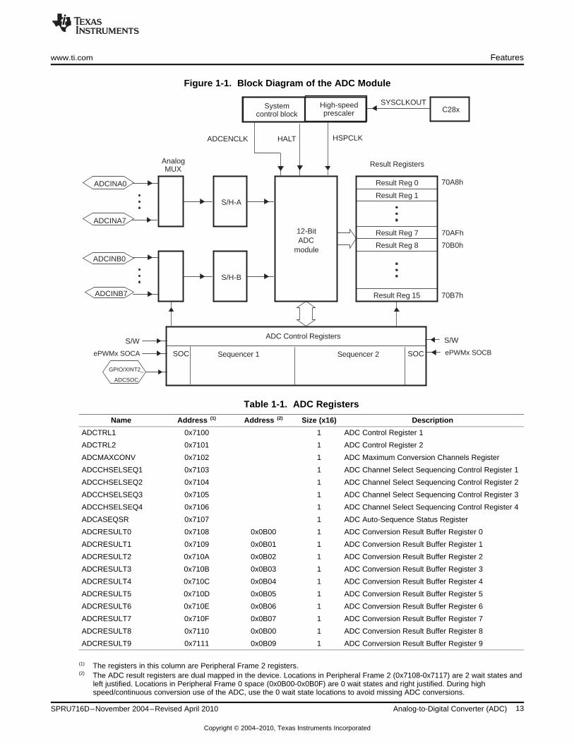
The sequencer operation for both 8-state and 16-state modes is almost identical; the few differences arehighlighted in Table 1-2.
18 Analog-to-Digital Converter (ADC) SPRU716D–November 2004–Revised April 2010
Copyright © 2004–2010, Texas Instruments Incorporated
www.ti.com Autoconversion Sequencer Principle of Operation
Table 1-2. Comparison of Single and Cascaded Operating Modes
Single 8-state sequencer #1 Single 8-state Cascaded 16-stateFeature (SEQ1) sequencer #2 (SEQ2) sequencer (SEQ)
Start-of-conversion (SOC) ePWMx SOCA, software, ePWMx SOCB, software ePWMx SOCA, ePWMxtriggers external pin SOCB, software,
external pin
Maximum number of 8 8 16autoconversions(i.e., sequence length)
Autostop at end-of- Yes Yes Yessequence (EOS)
Arbitration priority High Low Not applicable
ADC conversion result register 0 to 7 8 to 15 0 to 15locations
ADCCHSELSEQn bit field CONV00 to CONV07 CONV08 to CONV15 CONV00 to CONV15assignment
For convenience, the sequencer states will be subsequently referred to as:
• For SEQ1: CONV00 to CONV07• For SEQ2: CONV08 to CONV15• For Cascaded SEQ: CONV00 to CONV15
The analog input channel selected for each sequenced conversion is defined by CONVxx bit fields in theADC input channel select sequencing control registers (ADCCHSELSEQn). CONVxx is a 4-bit field thatspecifies any one of the 16 channels for conversion. Since a maximum of 16 conversions in a sequence ispossible when using the sequencers in cascaded mode, 16 such 4-bit fields (CONV00 - CONV15) areavailable and are spread across four 16-bit registers (ADCCHSELSEQ1 - ADCCHSELSEQ4). TheCONVxx bits can have any value from 0 to 15. The analog channels can be chosen in any desired orderand the same channel may be selected multiple times.
19SPRU716D–November 2004–Revised April 2010 Analog-to-Digital Converter (ADC)
Copyright © 2004–2010, Texas Instruments Incorporated
Autoconversion Sequencer Principle of Operation www.ti.com
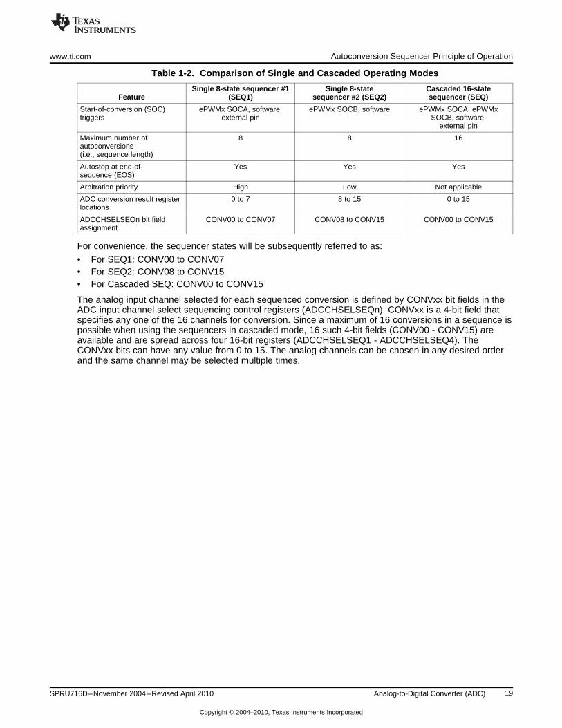
Example 1-1. Simultaneous Sampling Dual Sequencer Mode Example
Example initialization:AdcRegs.ADCTRL3.bit.SMODE_SEL = 0x1; // Setup simultaneous sampling mode
AdcRegs.ADCMAXCONV.all = 0x0033; // 4 double conv's each sequencer (8 total)
AdcRegs.ADCCHSELSEQ1.bit.CONV00 = 0x0; // Setup conv from ADCINA0 & ADCINB0
AdcRegs.ADCCHSELSEQ1.bit.CONV01 = 0x1; // Setup conv from ADCINA1 & ADCINB1
AdcRegs.ADCCHSELSEQ1.bit.CONV02 = 0x2; // Setup conv from ADCINA2 & ADCINB2
AdcRegs.ADCCHSELSEQ1.bit.CONV03 = 0x3; // Setup conv from ADCINA3 & ADCINB3
AdcRegs.ADCCHSELSEQ3.bit.CONV08 = 0x4; // Setup conv from ADCINA4 & ADCINB4
AdcRegs.ADCCHSELSEQ3.bit.CONV09 = 0x5; // Setup conv from ADCINA5 & ADCINB5
AdcRegs.ADCCHSELSEQ3.bit.CONV10 = 0x6; // Setup conv from ADCINA6 & ADCINB6
AdcRegs.ADCCHSELSEQ3.bit.CONV11 = 0x7; // Setup conv from ADCINA7 & ADCINB7
If SEQ1 and SEQ2 were both executed, the results would go to the following RESULT registers:ADCINA0 -> ADCRESULT0
ADCINB0 -> ADCRESULT1
ADCINA1 -> ADCRESULT2
ADCINB1 -> ADCRESULT3
ADCINA2 -> ADCRESULT4
ADCINB2 -> ADCRESULT5
ADCINA3 -> ADCRESULT6
ADCINB3 -> ADCRESULT7
ADCINA4 -> ADCRESULT8
ADCINB4 -> ADCRESULT9
ADCINA5 -> ADCRESULT10
ADCINB5 -> ADCRESULT11
ADCINA6 -> ADCRESULT12
ADCINB6 -> ADCRESULT13
ADCINA7 -> ADCRESULT14
ADCINB7 -> ADCRESULT15
20 Analog-to-Digital Converter (ADC) SPRU716D–November 2004–Revised April 2010
Copyright © 2004–2010, Texas Instruments Incorporated

www.ti.com Uninterrupted Autosequenced Mode
Example 1-2. Simultaneous Sampling Cascaded Sequencer Mode Example
AdcRegs.ADCTRL3.bit.SMODE_SEL = 0x1; // Setup simultaneous sampling mode
AdcRegs.ADCTRL1.bit.SEQ_CASC = 0x1; // Setup cascaded sequencer mode
AdcRegs.ADCMAXCONV.all = 0x0007; // 8 double conv's (16 total)
AdcRegs.ADCCHSELSEQ1.bit.CONV00 = 0x0; // Setup conv from ADCINA0 & ADCINB0
AdcRegs.ADCCHSELSEQ1.bit.CONV01 = 0x1; // Setup conv from ADCINA1 & ADCINB1
AdcRegs.ADCCHSELSEQ1.bit.CONV02 = 0x2; // Setup conv from ADCINA2 & ADCINB2
AdcRegs.ADCCHSELSEQ1.bit.CONV03 = 0x3; // Setup conv from ADCINA3 & ADCINB3
AdcRegs.ADCCHSELSEQ2.bit.CONV04 = 0x4; // Setup conv from ADCINA4 & ADCINB4
AdcRegs.ADCCHSELSEQ2.bit.CONV05 = 0x5; // Setup conv from ADCINA5 & ADCINB5
AdcRegs.ADCCHSELSEQ2.bit.CONV06 = 0x6; // Setup conv from ADCINA6 & ADCINB6
AdcRegs.ADCCHSELSEQ2.bit.CONV07 = 0x7; // Setup conv from ADCINA7 & ADCINB7
If the cascaded SEQ was executed, the results would go to the following ADCRESULT registers:ADCINA0 -> ADCRESULT0
ADCINB0 -> ADCRESULT1
ADCINA1 -> ADCRESULT2
ADCINB1 -> ADCRESULT3
ADCINA2 -> ADCRESULT4
ADCINB2 -> ADCRESULT5
ADCINA3 -> ADCRESULT6
ADCINB3 -> ADCRESULT7
ADCINA4 -> ADCRESULT8
ADCINB4 -> ADCRESULT9
ADCINA5 -> ADCRESULT10
ADCINB5 -> ADCRESULT11
ADCINA6 -> ADCRESULT12
ADCINB6 -> ADCRESULT13
ADCINA7 -> ADCRESULT14
ADCINB7 -> ADCRESULT15
1.3 Uninterrupted Autosequenced Mode
The following description applies to the 8-state sequencers (SEQ1 or SEQ2). In this mode, SEQ1/SEQ2can autosequence up to eight conversions of any channel in a single sequencing session (16 whensequencers are cascaded together). Figure 1-6 shows the flow diagram. The result of each conversion isstored in one of the eight result registers (ADCRESULT0 - ADCRESULT7 for SEQ1 and ADCRESULT8 -ADCRESULT15 for SEQ2). These registers are filled from the lowest address to the highest address.
The number of conversions in a sequence is controlled by MAX_CONVn (a 3-bit or 4-bit field in theADCMAXCONV register), which is automatically loaded into the sequencing counter status bits(SEQ_CNTR[3:0]) in the autosequence status register (ADCASEQSR) at the start of an autosequencedconversion session. The MAX_CONVn field can have a value ranging from zero to seven (zero to fifteenwhen sequencers are cascaded together). SEQ_CNTR bits count down from their loaded value as thesequencer starts from state CONV00 and continues sequentially (CONV01, CONV02, and so on) untilSEQ_CNTR has reached zero. The number of conversions completed during an autosequencing sessionis equal to (MAX_CONVn + 1).
Example 1-3. Conversion in Dual-Sequencer Mode Using SEQ1
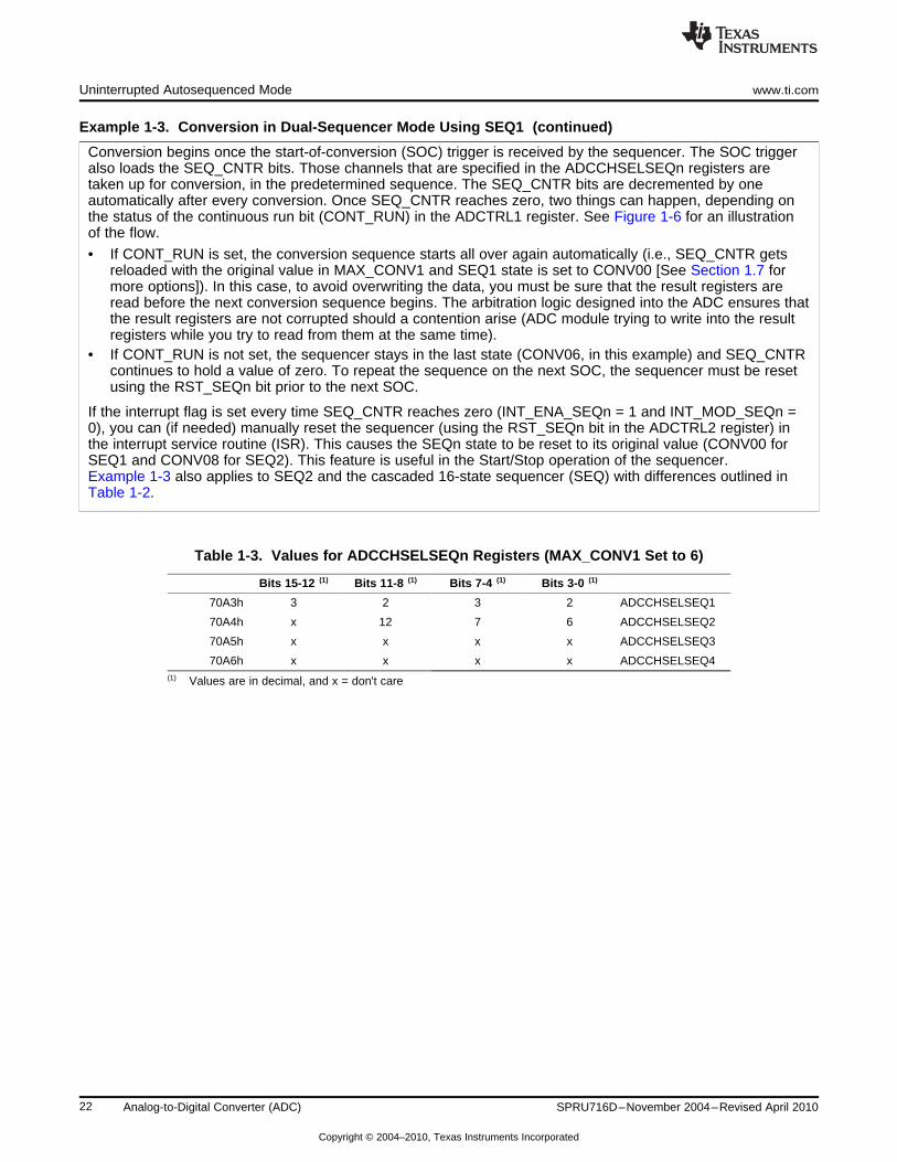
Suppose seven conversions are desired from SEQ1 (i.e., inputs ADCINA2 and ADCINA3 twice, thenADCINA6, ADCINA7, and ADCINB4 must be converted as part of the autosequenced session), thenMAX_CONV1 should be set to 6 and the ADCCHSELSEQn registers should be set to the values shown inTable 1-3.
21SPRU716D–November 2004–Revised April 2010 Analog-to-Digital Converter (ADC)
Copyright © 2004–2010, Texas Instruments Incorporated
Uninterrupted Autosequenced Mode www.ti.com
Example 1-3. Conversion in Dual-Sequencer Mode Using SEQ1 (continued)
Conversion begins once the start-of-conversion (SOC) trigger is received by the sequencer. The SOC triggeralso loads the SEQ_CNTR bits. Those channels that are specified in the ADCCHSELSEQn registers aretaken up for conversion, in the predetermined sequence. The SEQ_CNTR bits are decremented by oneautomatically after every conversion. Once SEQ_CNTR reaches zero, two things can happen, depending onthe status of the continuous run bit (CONT_RUN) in the ADCTRL1 register. See Figure 1-6 for an illustrationof the flow.
• If CONT_RUN is set, the conversion sequence starts all over again automatically (i.e., SEQ_CNTR getsreloaded with the original value in MAX_CONV1 and SEQ1 state is set to CONV00 [See Section 1.7 formore options]). In this case, to avoid overwriting the data, you must be sure that the result registers areread before the next conversion sequence begins. The arbitration logic designed into the ADC ensures thatthe result registers are not corrupted should a contention arise (ADC module trying to write into the resultregisters while you try to read from them at the same time).
• If CONT_RUN is not set, the sequencer stays in the last state (CONV06, in this example) and SEQ_CNTRcontinues to hold a value of zero. To repeat the sequence on the next SOC, the sequencer must be resetusing the RST_SEQn bit prior to the next SOC.
If the interrupt flag is set every time SEQ_CNTR reaches zero (INT_ENA_SEQn = 1 and INT_MOD_SEQn =0), you can (if needed) manually reset the sequencer (using the RST_SEQn bit in the ADCTRL2 register) inthe interrupt service routine (ISR). This causes the SEQn state to be reset to its original value (CONV00 forSEQ1 and CONV08 for SEQ2). This feature is useful in the Start/Stop operation of the sequencer.Example 1-3 also applies to SEQ2 and the cascaded 16-state sequencer (SEQ) with differences outlined inTable 1-2.
Table 1-3. Values for ADCCHSELSEQn Registers (MAX_CONV1 Set to 6)
Bits 15-12 (1) Bits 11-8 (1) Bits 7-4 (1) Bits 3-0 (1)
70A3h 3 2 3 2 ADCCHSELSEQ1
70A4h x 12 7 6 ADCCHSELSEQ2
70A5h x x x x ADCCHSELSEQ3
70A6h x x x x ADCCHSELSEQ4(1) Values are in decimal, and x = don't care
22 Analog-to-Digital Converter (ADC) SPRU716D–November 2004–Revised April 2010
Copyright © 2004–2010, Texas Instruments Incorporated

Current conversion complete.Digital result is written into
corresponding ADCRESULTn register
Conversion begins. SEQ_CNTR bits are decremented by
one for every conversion
MAX_CONVn value gets loaded into SEQ_CNTR bits in ADCASEQSR register
SOC trigger arrives
Initialize the ADC registers
Allconversions complete?
(SEQ_CNTR = 0?)
Set INT_SEQn
Stop
No
Yes
www.ti.com Uninterrupted Autosequenced Mode
Figure 1-6. Flow Chart for Uninterrupted Autosequenced Mode
A The flow chart corresponds to CONT_RUN bit = 0 and INT_MOD_SEQn bit = 0.
1.3.1 Sequencer Start/Stop Mode (Sequencer Start/Stop Operation With MultipleTime-Sequenced Triggers)
In addition to the uninterrupted autosequenced mode, any sequencer (SEQ1, SEQ2, or SEQ) can beoperated in a Stop/Start mode which is synchronized to multiple start-of-conversion (SOC) triggers,separated in time. This mode is similar to Example 1-3, but the sequencer is allowed to be retriggeredwithout being reset to the initial state CONV00, once it has completed its first sequence (i.e., thesequencer is not reset in the interrupt service routine). Therefore, when one conversion sequence ends,the sequencer stays in the current conversion state. The continuous run bit (CONT_RUN) in theADCTRL1 register must be set to zero (i.e., disabled) for this mode.
23SPRU716D–November 2004–Revised April 2010 Analog-to-Digital Converter (ADC)
Copyright © 2004–2010, Texas Instruments Incorporated

25 µs
50 µs
ePWMcounter
PWM A/Boutput
I1, I2, I3 V1, V2,V3 I1, I2, I3 V1, V2, V3
Uninterrupted Autosequenced Mode www.ti.com
Example 1-4. Sequencer Start/Stop Operation
Requirement: To start three autoconversions (e.g., I1,I2,I3) off trigger 1 (underflow) and threeautoconversions (e.g., V1,V2,V3) off trigger 2 (period). Triggers 1 and 2 are separated in time by 25 µs andare provided by an ePWM. See Figure 1-7. Only SEQ1 is used in this case.
NOTE: Triggers 1 and 2 may be an SOC signal from ePWM, external pin, or software. The sametrigger source may occur twice to satisfy the dual-trigger requirement of this example. Caremust be taken such that multiple ePWM triggers are not lost due sequences already inprogress. See Section 1.3.3.
Here MAX_CONV1 is set to 2 and the ADC Input Channel Select Sequencing Control Registers(ADCCHSELSEQn) are set as shown in Table 1-4.
Once reset and initialized, SEQ1 waits for a trigger. With the first trigger, three conversions withchannel-select values of: CONV00 (I1), CONV01 (I2), and CONV02 (I3) are performed. SEQ1 then waits atcurrent state for another trigger. Twenty-five microseconds later when the second trigger arrives, anotherthree conversions occur, with channel-select values of CONV03 (V1), CONV04 (V2), and CONV05 (V3).
The value of MAX_CONV1 is automatically loaded into SEQ_CNTR for both trigger cases. If a differentnumber of conversions are required at the second trigger point, you must (at some appropriate time beforethe second trigger) change the value of MAX_CONV1 through software, otherwise, the current (originallyloaded) value will be reused. This can be done by an ISR that changes the value of MAX_CONV1 at theappropriate time. The interrupt operation modes are described in Section 1.3.4.
At the end of the second autoconversion session, the ADC result registers will have the values shown inTable 1-5.
At this point, SEQ1 keeps "waiting" at the current state for another trigger. Now, the user can reset SEQ1(by software) to state CONV00 and repeat the same trigger1, 2 sessions.
Figure 1-7. Example of ePWM Triggers to Start the Sequencer
Table 1-4. Values for ADCCHSELSEQn (MAX_CONV1 set to 2)
Bits 15-12 Bits 11-8 Bits 7-4 Bits 3-0
70A3h V1 I3 I2 I1 ADCCHSELSEQ1
70A4h x x V3 V2 ADCCHSELSEQ2
70A5h x x x x ADCCHSELSEQ3
70A6h x x x x ADCCHSELSEQ4
24 Analog-to-Digital Converter (ADC) SPRU716D–November 2004–Revised April 2010
Copyright © 2004–2010, Texas Instruments Incorporated

www.ti.com Uninterrupted Autosequenced Mode
Table 1-5. Values After Second AutoconversionSession
Buffer Register ADC Conversion Result Buffer
ADCRESULT0 I1
ADCRESULT1 I2
ADCRESULT2 I3
ADCRESULT3 V1
ADCRESULT4 V2
ADCRESULT5 V3
ADCRESULT6 x
ADCRESULT7 x
ADCRESULT8 x
ADCRESULT9 x
ADCRESULT10 x
ADCRESULT11 x
ADCRESULT12 x
ADCRESULT13 x
ADCRESULT14 x
ADCRESULT15 x
1.3.2 Simultaneous Sampling Mode
The ADC has the ability to sample two ADCINxx inputs simultaneously, provided that one input is from therange ADCINA0 - ADCINA7 and the other input is from the range ADCINB0 - ADCINB7. Furthermore, thetwo inputs must have the same sample-and-hold offset (i.e., ADCINA4 and ADCINB4, but not ADCINA7and ADCINB6). To put the ADC into simultaneous sampling mode, the SMODE_SEL bit in the ADCTRL3register must be set. See Section 1.2 for details.
1.3.3 Input Trigger Description
Each sequencer has a set of trigger inputs that can be enabled/disabled. See Table 1-6 for the valid inputtriggers for SEQ1, SEQ2, and cascaded SEQ.
Table 1-6. Input Triggers
SEQ1 (sequencer 1) SEQ2 (sequencer 2) Cascaded SEQ
Software trigger (software SOC) Software trigger (software SOC) Software trigger (software SOC)
ePWMx SOCA ePWMx SOCB ePWMx SOCA
XINT2_ADCSOC ePWMx SOCB
XINT2_ADCSOC
25SPRU716D–November 2004–Revised April 2010 Analog-to-Digital Converter (ADC)
Copyright © 2004–2010, Texas Instruments Incorporated

Uninterrupted Autosequenced Mode www.ti.com
NOTE:• An SOC trigger can initiate an autoconversion sequence whenever a sequencer is in an
idle state. An idle state is either CONV00 prior to receiving a trigger, or any state whichthe sequencer lands on at the completion of a conversion sequence, i.e., whenSEQ_CNTR has reached a count of zero.
• If an SOC trigger occurs while a current conversion sequence is underway, it sets theSOC_SEQn bit (which would have been cleared on the commencement of a previousconversion sequence) in the ADCTRL2 register. If yet another SOC trigger occurs, it islost (i.e., when the SOC_SEQn bit is already set (SOC pending), subsequent triggerswill be ignored).
• Once triggered, the sequencer cannot be stopped/halted in mid sequence. The programmust either wait until an end-of-sequence (EOS) or initiate a sequencer reset, whichbrings the sequencer immediately back to the idle start state (CONV00 for SEQ1 andcascaded cases; CONV08 for SEQ2).
• When SEQ1/2 are used in cascaded mode, triggers going to SEQ2 are ignored, whileSEQ1 triggers are active. Cascaded mode can be viewed as SEQ1 with 16 statesinstead of eight.
1.3.4 Interrupt Operation During Sequenced Conversions
The sequencer can generate interrupts under two operating modes. These modes are determined by theInterrupt-Mode-Enable control bits in ADCTRL2.
A variation of Example 1-4 can be used to show how interrupt mode 1 and mode 2 are useful underdifferent operating conditions.
Case 1: Number of samples in the first and second sequences are not equal
• Mode 1 Interrupt operation (i.e., Interrupt request occurs at every EOS)
1. Sequencer is initialized with MAX_CONVn = 1 for converting I1 and I22. At ISR "a", MAX_CONVn is changed to 2 (by software) for converting V1, V2, and V3
3. At ISR "b", the following events take place :
(a) MAX_CONVn is changed to 1 again for converting I1 and I2.(b) Values I1, I2, V1, V2, and V3 are read from ADC result registers.(c) The sequencer is reset.
4. Steps 2 and 3 are repeated. Note that the interrupt flag is set every time SEQ_CNTR reaches zeroand both interrupts are recognized.
Case 2: Number of samples in the first and second sequences are equal
• Mode 2 Interrupt operation (i.e., Interrupt request occurs at every other EOS)
1. Sequencer is initialized with MAX_CONVn = 2 for converting I1, I2, and I3 (or V1, V2, and V3).2. At ISR "b" and "d", the following events take place :
(a) Values I1, I2, I3,V1, V2, and V3 are read from ADC result registers.(b) The sequencer is reset.
3. Step 2 is repeated.
Case 3: Number of samples in the first and second sequences are equal (with dummy read)
• Mode 2 Interrupt operation (i.e., Interrupt request occurs at every other EOS)
1. Sequencer is initialized with MAX_CONVn = 2 for I1, I2, and x(dummy sample).2. At ISR "b" and "d", the following events take place :
(a) Values I1, I2, x,V1, V2, and V3 are read from ADC result registers.(b) The sequencer is reset.
3. Step 2 is repeated. Note that the third I-sample (x) is a dummy sample, and is not really required.However, to minimize ISR overhead and CPU intervention, advantage is taken of the "every other"Interrupt request feature of Mode 2.
26 Analog-to-Digital Converter (ADC) SPRU716D–November 2004–Revised April 2010
Copyright © 2004–2010, Texas Instruments Incorporated

25 µs
50 µs
ePWMcounter
PWM A/Boutput
“a” “b” “c” “d”
Samplingrequest
SEQinterrupt
Case 1
I1,I2,I3
“b”
I1,I2,I3 V1,V2,V3
“d”
V1,V2,V3Case 2
“b” “d”
Case 3
I1,I2I1,I2 V1,V2,V3 V1,V2,V3
I1,I2,xI1,I2,x V1,V2,V3 V1,V2,V3
Samplingrequest
SEQinterrupt
Samplingrequest
SEQinterrupt
www.ti.com Uninterrupted Autosequenced Mode
Figure 1-8. Interrupt Operation During Sequenced Conversions
27SPRU716D–November 2004–Revised April 2010 Analog-to-Digital Converter (ADC)
Copyright © 2004–2010, Texas Instruments Incorporated
4-bit clockdivider
(x1, 1/2, ... 1/30)HSPCLK
ADCTRL3[4-1](ADCLKPS[3-0])
x1/2
x1
ADCTRL1[7]=1(CPS=1)
ADCTRL1[7]=0(CPS=0)
SOC pulsegenerator
S/H clock pulse
ADCCLK
ADCTRL1[11-8](ACQ_PS[3-0])
PLLXCLKIN
SH clock/pulse
No PLLHISPCP
������
ADCLKPS CPS ADCCLK
ACQ_PSADCENCLKPCLKCR[3]
��
ADC Clock Prescaler www.ti.com
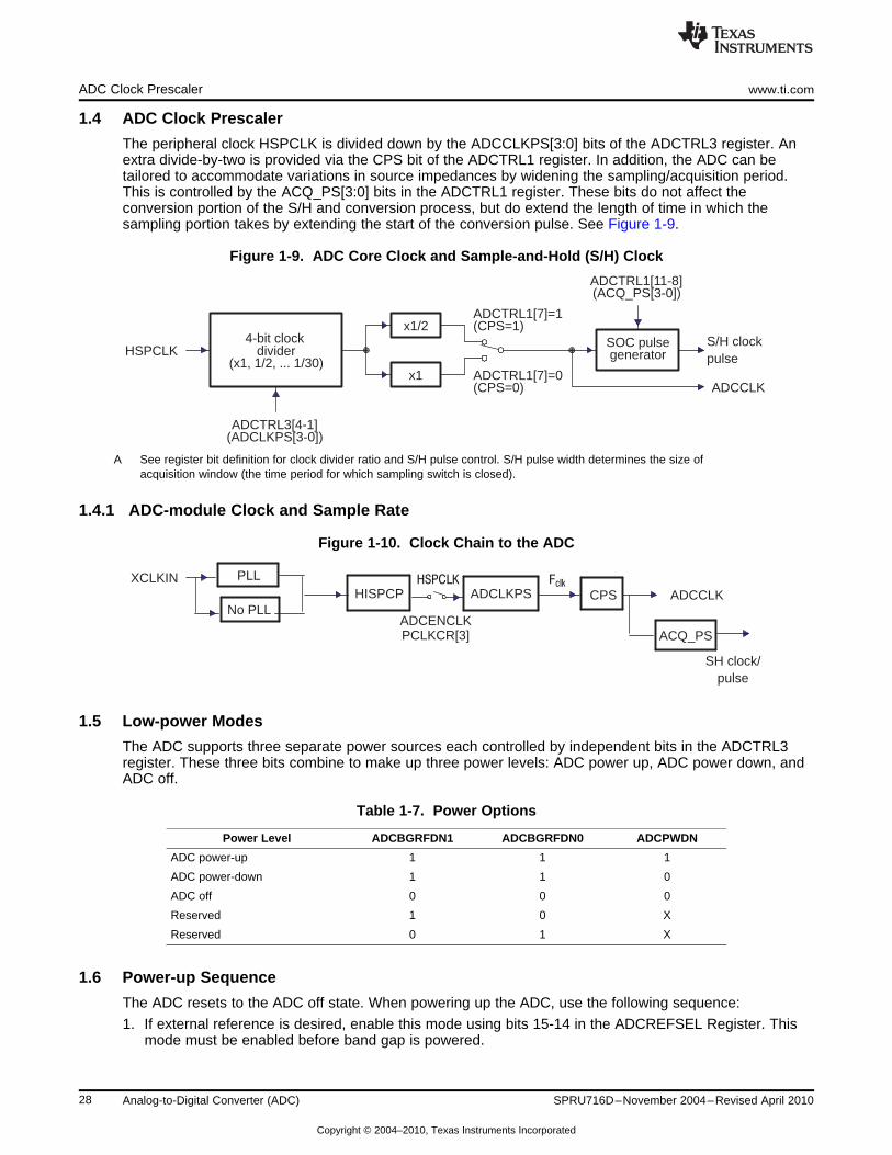
1.4 ADC Clock Prescaler
The peripheral clock HSPCLK is divided down by the ADCCLKPS[3:0] bits of the ADCTRL3 register. Anextra divide-by-two is provided via the CPS bit of the ADCTRL1 register. In addition, the ADC can betailored to accommodate variations in source impedances by widening the sampling/acquisition period.This is controlled by the ACQ_PS[3:0] bits in the ADCTRL1 register. These bits do not affect theconversion portion of the S/H and conversion process, but do extend the length of time in which thesampling portion takes by extending the start of the conversion pulse. See Figure 1-9.
Figure 1-9. ADC Core Clock and Sample-and-Hold (S/H) Clock
A See register bit definition for clock divider ratio and S/H pulse control. S/H pulse width determines the size ofacquisition window (the time period for which sampling switch is closed).
1.4.1 ADC-module Clock and Sample Rate
Figure 1-10. Clock Chain to the ADC
1.5 Low-power Modes
The ADC supports three separate power sources each controlled by independent bits in the ADCTRL3register. These three bits combine to make up three power levels: ADC power up, ADC power down, andADC off.
Table 1-7. Power Options
Power Level ADCBGRFDN1 ADCBGRFDN0 ADCPWDN
ADC power-up 1 1 1
ADC power-down 1 1 0
ADC off 0 0 0
Reserved 1 0 X
Reserved 0 1 X
1.6 Power-up Sequence
The ADC resets to the ADC off state. When powering up the ADC, use the following sequence:
1. If external reference is desired, enable this mode using bits 15-14 in the ADCREFSEL Register. Thismode must be enabled before band gap is powered.
28 Analog-to-Digital Converter (ADC) SPRU716D–November 2004–Revised April 2010
Copyright © 2004–2010, Texas Instruments Incorporated

www.ti.com Sequencer Override Feature
2. Power up the reference, bandgap, and analog circuits together by setting bits 7-5 (ADCBGRFDN[1:0],ADCPWDN) in the ADCTRL3 register.
3. Before performing the first conversion, a delay of 5 ms is required.
When powering down the ADC, all three bits can be cleared simultaneously. The ADC power level mustbe controlled via software and they are independent of the state of the device power modes.
Sometimes it is desirable to power down the ADC while leaving the band-gap and reference powered byclearing the ADCPWDN bit only. When the ADC is re-powered, a delay of 20 ms is required after this bit isset before performing any conversions.
NOTE: The 280x ADC requires a 5-ms delay after all of the circuits are powered up. This differsfrom the 281x ADC.
1.7 Sequencer Override Feature
In normal operation, sequencers SEQ1, SEQ2 or cascaded SEQ1 help to convert selected ADC channelsand store them in the respective ADCRESULTn registers, sequentially. The sequence naturally wrapsaround at the end of the MAX_CONVn setting. With the sequencer override feature, the naturalwraparound of the sequencers can be controlled in software. The sequencer override feature is controlledby bit 5 of the ADC Control Register 1 (ADCCTRL1).
For example, assume the SEQ_OVRD bit is 0 and the ADC is in cascaded-sequencer,continuous-conversion mode with MAX_CONV1 set to 7. Normally, the sequencer would incrementsequentially and update up to ADCRESULT7 register with ADC conversions and wraps around to 0. At theend of the ADCRESULT7 register update, the relevant interrupt flag would be set.
With the SEQ_OVRD bit set to 1, the sequencer updates seven result registers and does not wrap aroundto 0. Instead, the sequencer will increment sequentially and update the ADCRESULT8 register onwardsuntil the ADCRESULT15 register is reached. After updating ADCRESULT15 register, the natural wraparound to 0 will occur. This feature treats the result registers (0-15) like a FIFO for sequential data capturefrom the ADC. This feature is very helpful to capture ADC data when ADC conversions are done at themaximum data rate.
29SPRU716D–November 2004–Revised April 2010 Analog-to-Digital Converter (ADC)
Copyright © 2004–2010, Texas Instruments Incorporated

Bandgapreference
ADC REFSELADC reference
ADCREFIN
F280x DSP
ADCRESEXT(A)
ADCREFP(A)
ADCREFM(A)
ADC LO
2.048-V reference
Analog ground
Internal/External Reference Voltage Selection www.ti.com
Recommendations and caution on sequencer override feature:• After reset, SEQ_OVRD bit will be 0; therefore the sequencer override feature remains disabled.• When SEQ _OVRD bit is set for all nonzero values of MAX_CONVn, the related interrupt flag bit will
be set for every MAX_CONVn count of result register update.• For example, if ADCMAXCONV is set to 3, then the interrupt flag for the selected sequencer will be set
every four result register updates. The wraparound always occurs at the end of the sequencer (i.e.,after ADCRESULT15 register update in cascaded sequencer mode).
• This will be functional in conversions using SEQ1, SEQ2, and cascaded sequencers using SEQ1.• It is recommended that this feature not be enabled/controlled dynamically within the program. Always
enable this feature during the ADC module initialization.• In continuous-conversion mode with sequencer changes, the ADC channel address uses the preset
values in CONVxx registers. If continuous conversions of the same channel are needed then all theCONVxx registers should have the same channel address.
• In continuous-conversion mode, if a sequencer reset is needed: set CONT_RUN bit to 0, wait 2 cyclesin the ADC Clock domain, then reset the sequencer. CONT_RUN can then be set back to 1.
• For example, to get 16 contiguous samples for the ADCINA0 channel using the sequencer overridefeature, all 16 CONVxx registers should be set to 0x0000.
1.8 Internal/External Reference Voltage Selection
By default, an internally generated bandgap voltage reference is selected to supply the ADC logic.
Based on customer application requirements, the ADC logic may be supplied by an external voltagereference. The ADC will accept 2.048 V, 1.5 V, or 1.024 V on the ADCREFIN pin. The value of theADCREFSEL register determines the reference source selected.
If the internal reference option is chosen, the ADCREFIN pin can be left connected to the selected source,left floating, or grounded. Regardless of which option is chosen, the external circuit for the ADCRESEXT,ADCREFP, and ADCREFM pins is the same.
The external reference voltage of 2.048 V was chosen to match industry standard reference components.These components are available in various temperature ratings. A recommended Texas Instruments partis REF3020AIDBZ.
Figure 1-11. External Bias for 2.048-V External Reference
30 Analog-to-Digital Converter (ADC) SPRU716D–November 2004–Revised April 2010
Copyright © 2004–2010, Texas Instruments Incorporated

Convert ADCLO reference
~20 conversions
Areany codes
0?
Yes
No
Calculate the average output code of the
conversions
Subtract the average from the value in the OFFTRIM
register and write result backto the OFFTRIM register
Add 40 (decimal) to the OFFTRIM
register
www.ti.com Offset Error Correction
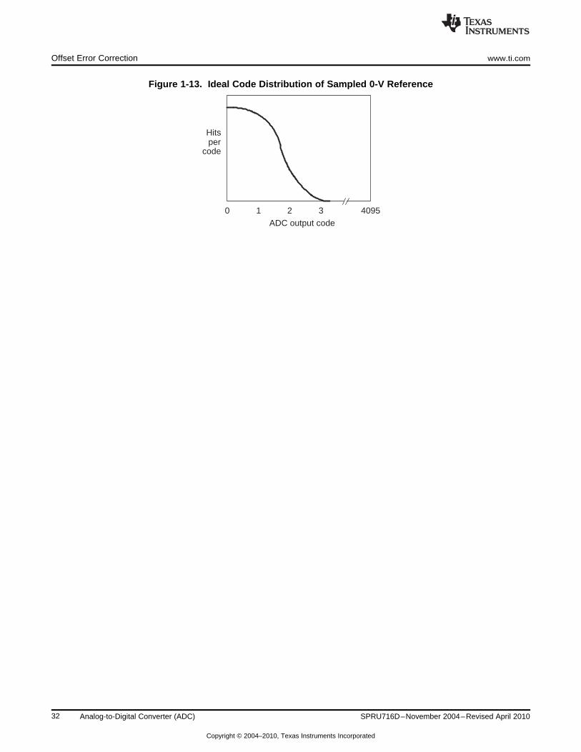
1.9 Offset Error Correction
The 280x ADC supports offset correction via a 9-bit field in the ADC Offset Trim Register(ADCOFFTRIM).The value contained in this register will be added/subtracted before the results are available in the ADCresult registers. This operation is contained in the ADC module, so timing for results will not be affected.Furthermore, since the operation is handled inside the ADC, the full dynamic range of the ADC will bemaintained for any trim value.
Figure 1-12. Flow Chart of Offset Error Correction Process
Example 1-5. Negative Offset
At startup, most of the reference conversions yield a zero result. After writing the value 0x28 (40 decimal)into the OFFTRIM register, all of the reference conversions give a positive result and average out to 0x19(25 decimal). The final value written to the OFFTRIM register should be 0x0F (15 decimal).
Example 1-6. Positive Offset
At startup, all of the reference conversions yield a positive result with an average of 0x14 (20 decimal).The final value written to the OFFTRIM register should be 0x1EC (-20 decimal).
After the offset error correction process is completed, a half bell curved distribution similar to Figure 1-13should be seen when multiple ADCLO samples are converted. The other half of the bell curve is hiddendue to the fact that the converter bottoms out at a code of zero.
31SPRU716D–November 2004–Revised April 2010 Analog-to-Digital Converter (ADC)
Copyright © 2004–2010, Texas Instruments Incorporated
Hitsper
code
0 1 2 3 4095ADC output code
Offset Error Correction www.ti.com
Figure 1-13. Ideal Code Distribution of Sampled 0-V Reference
32 Analog-to-Digital Converter (ADC) SPRU716D–November 2004–Revised April 2010
Copyright © 2004–2010, Texas Instruments Incorporated

Chapter 2SPRU716D–November 2004–Revised April 2010
ADC Registers
This chapter contains the ADC registers and bit definitions, with the registers grouped by function.
Topic ........................................................................................................................... Page
2.1 ADC Control Registers ....................................................................................... 342.2 Maximum Conversion Channels Register (ADCMAXCONV) .................................... 382.3 Autosequence Status Register (ADCASEQSR) ...................................................... 402.4 ADC Status and Flag Register (ADCST) ............................................................... 412.5 ADC Reference Select Register (ADCREFSEL) ...................................................... 422.6 ADC Offset Trim Register (ADCOFFTRIM) ............................................................ 422.7 ADC Input Channel Select Sequencing Control Registers ...................................... 432.8 ADC Conversion Result Buffer Registers (ADCRESULTn) ...................................... 44
33SPRU716D–November 2004–Revised April 2010 ADC Registers
Copyright © 2004–2010, Texas Instruments Incorporated

ADC Control Registers www.ti.com
2.1 ADC Control Registers
Figure 2-1. ADC Control Register 1 (ADCTRL1) (Address Offset 00h)15 14 13 12 11 8
Reserved RESET SUSMOD ACQ_PS
R-0 R/W-0 R/W-0 R/W-0
7 6 5 4 3 0
CPS CONT_RUN SEQ_OVRD SEQ_CASC Reserved
R/W-0 R/W-0 R/W-0 R/W-0 R-0
LEGEND: R/W = Read/Write; R = Read only; -n = value after reset
Table 2-1. ADC Control Register 1 (ADCTRL1) Field Descriptions
Bit(s) Name Value Description
15 Reserved Reads return a zero. Writes have no effect.
14 RESET ADC module software reset. This bit causes a master reset on the entire ADC module.All register bits and sequencer state machines are reset to the initial state as occurswhen the device reset pin is pulled low (or after a power-on reset). This is aone-time-effect bit, meaning this bit is self-cleared immediately after it is set to 1. Readof this bit always returns a 0. Also, the reset of ADC has a latency of two clock cycles(that is, other ADC control register bits should not be modified until two ADC clockcycles after the instruction that resets the ADC.
0 No effect
1 Resets entire ADC module (bit is then set back to 0 by ADC logic)
13-12 SUSMOD[1:0] Emulation-suspend mode. These bits determine what occurs when anemulation-suspend occurs (due to the debugger hitting a breakpoint, for example).
00 Mode 0. Emulation suspend is ignored.
01 Mode 1. Sequencer and other wrapper logic stops after current sequence is complete,final result is latched, and state machine is updated.
10 Mode 2. Sequencer and other wrapper logic stops after current conversion is complete,result is latched, and state machine is updated.
11 Mode 3. Sequencer and other wrapper logic stops immediately on emulation suspend.
11-8 ACQ_PS[3:0] Acquisition window size. This bit field controls the width of SOC pulse, which, in turn,determines for what time duration the sampling switch is closed. The width of SOC pulseis ADCTRL1[11:8] + 1 times the ADCLK period.
7 CPS Core clock prescaler. The prescaler is applied to divided device peripheral clock,HSPCLK.
0 ADCCLK = Fclk/1
1 ADCCLK = Fclk/2
Note: Fclk = Prescaled HSPCLK (ADCCLKPS[3:0])
6 CONT_RUN Continuous run. This bit determines whether the sequencer operates in continuousconversion mode or start-stop mode. This bit can be written while a current conversionsequence is active. This bit will take effect at the end of the current conversionsequence; i.e., software can set/clear this bit until EOS has occurred, for valid action tobe taken. In the continuous conversion mode, there is no need to reset the sequencer;however, the sequencer must be reset in the start-stop mode to put the converter instate CONV00.
0 Start-stop mode. Sequencer stops after reaching EOS. On the next SOC, the sequencerstarts from the state where it ended unless a sequencer reset is performed.
1 Continuous conversion mode. After reaching EOS, the behavior of the sequencerdepends on the state of the SEQ_OVRD bit. If this bit is cleared, the sequencer startsover again from its reset state (CONV00 for SEQ1 and cascaded, CONV08 for SEQ2). IfSEQ_OVRD is set, the sequencer starts again from its current position, withoutresetting.
5 SEQ_OVRD Sequencer override. Provides additional sequencer flexibility in continuous run mode byoverriding the wrapping around at the end of conversions set by MAX_CONVn.
0 Disabled - Allows the sequencer to wrap around at the end of conversions set byMAX_CONVn.
34 ADC Registers SPRU716D–November 2004–Revised April 2010
Copyright © 2004–2010, Texas Instruments Incorporated

www.ti.com ADC Control Registers
Table 2-1. ADC Control Register 1 (ADCTRL1) Field Descriptions (continued)
Bit(s) Name Value Description
1 Enabled - Overrides the sequencer from wrapping around at the end of conversions setby MAX_CONVn. Wraparound occurs only at the end of the sequencer.
4 SEQ_CASC Cascaded sequencer operation. This bit determines whether SEQ1 and SEQ2 operateas two 8-state sequencers or as a single 16-state sequencer (SEQ).
0 Dual-sequencer mode. SEQ1 and SEQ2 operate as two 8-state sequencers.
1 Cascaded mode. SEQ1 and SEQ2 operate as a single 16-state sequencer (SEQ).
3-0 Reserved Reads return zero. Writes have no effect.
Figure 2-2. ADC Control Register 2 (ADCTRL2) (Address Offset 01h)15 14 13 12 11 10 9 8
ePWM_SOCB_SEQ RST_SEQ1 SOC_SEQ1 Reserved INT_ENA_SEQ1 INT_MOD_SEQ1 Reserved ePWM_SOCA_SEQ1
R/W-0 R/W-0 R/W-0 R-0 R/W-0 R/W-0 R-0 R/W-0
7 6 5 4 3 2 1 0
EXT_SOC_SEQ1 RST_SEQ2 SOC_SEQ2 Reserved INT_ENA_SEQ2 INT_MOD_SEQ2 Reserved ePWM_SOCB_SEQ2
R/W-0 R/W-0 R/W-0 R-0 R/W-0 R/W-0 R-0 R/W-0
LEGEND: R/W = Read/Write; R = Read only; W = Write access, S = Set only, C = Clear -n = value after reset
Table 2-2. ADC Control Register 2 (ADCTRL2) Field Descriptions
Bit(s) Name Value Description
15 ePWM_SOCB_SEQ ePWM SOCB enable for cascaded sequencer (Note: This bit is active only in cascadedmode.)
0 No action
1 Setting this bit allows the cascaded sequencer to be started by an ePWM SOCB signal.The ePWM modules can be programmed to start a conversion on various events. See theTMS320x28xx , 28xxx Enhanced Pulse Width Modulation Module Reference Guide(literature number SPRU791) for more information on the ePWM modules.
14 RST_SEQ1 Reset sequencer1 Writing a 1 to this bit resets SEQ1 or the cascaded sequencerimmediately to an initial "pretriggered" state, i.e., waiting for a trigger at CONV00. Acurrently active conversion sequence will be aborted.
0 No action
1 Immediately reset sequencer to state CONV00
13 SOC_SEQ1 Start-of-conversion (SOC) trigger for Sequencer 1 (SEQ1) or the cascaded sequencer.This bit can be set by the following triggers:
• S/W - Software writing a 1 to this bit• ePWM SOCA• ePWM SOCB (only in cascaded mode)• EXT - External pin (i.e., GPIO Port A pin (GPIO31-0) configured as XINT2 in the
GPIOxINT2SEL register.See the for details on how to configure a GPIO pin as XINT2. When a trigger occurs,there are three possibilities:Case 1: SEQ1 idle and SOC bit clear SEQ1 starts immediately (under arbiter control).This bit is set and cleared, allowing for any "pending" trigger requests.Case 2: SEQ1 busy and SOC bit clear Bit is set signifying a trigger request is pending.When SEQ1 finally starts after completing current conversion, this bit is cleared.Case 3: SEQ1 busy and SOC bit set Any trigger occurring in this case is ignored (lost).
0 Clears a pending SOC trigger.Note: If the sequencer has already started, this bit is automatically cleared, and hence,writing a zero has no effect; i.e., an already started sequencer cannot be stopped byclearing this bit.
1 Software trigger - Start SEQ1 from currently stopped position (i.e., Idle mode)
35SPRU716D–November 2004–Revised April 2010 ADC Registers
Copyright © 2004–2010, Texas Instruments Incorporated
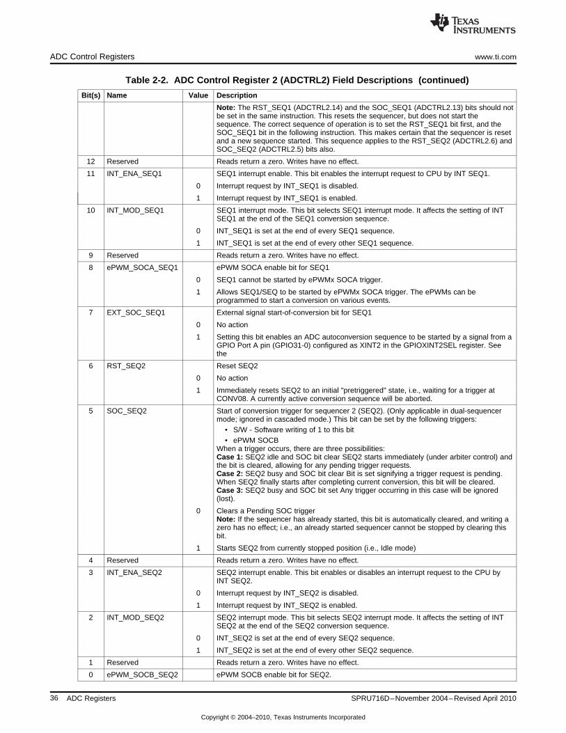
ADC Control Registers www.ti.com
Table 2-2. ADC Control Register 2 (ADCTRL2) Field Descriptions (continued)
Bit(s) Name Value Description
Note: The RST_SEQ1 (ADCTRL2.14) and the SOC_SEQ1 (ADCTRL2.13) bits should notbe set in the same instruction. This resets the sequencer, but does not start thesequence. The correct sequence of operation is to set the RST_SEQ1 bit first, and theSOC_SEQ1 bit in the following instruction. This makes certain that the sequencer is resetand a new sequence started. This sequence applies to the RST_SEQ2 (ADCTRL2.6) andSOC_SEQ2 (ADCTRL2.5) bits also.
12 Reserved Reads return a zero. Writes have no effect.
11 INT_ENA_SEQ1 SEQ1 interrupt enable. This bit enables the interrupt request to CPU by INT SEQ1.
0 Interrupt request by INT_SEQ1 is disabled.
1 Interrupt request by INT_SEQ1 is enabled.
10 INT_MOD_SEQ1 SEQ1 interrupt mode. This bit selects SEQ1 interrupt mode. It affects the setting of INTSEQ1 at the end of the SEQ1 conversion sequence.
0 INT_SEQ1 is set at the end of every SEQ1 sequence.
1 INT_SEQ1 is set at the end of every other SEQ1 sequence.
9 Reserved Reads return a zero. Writes have no effect.
8 ePWM_SOCA_SEQ1 ePWM SOCA enable bit for SEQ1
0 SEQ1 cannot be started by ePWMx SOCA trigger.
1 Allows SEQ1/SEQ to be started by ePWMx SOCA trigger. The ePWMs can beprogrammed to start a conversion on various events.
7 EXT_SOC_SEQ1 External signal start-of-conversion bit for SEQ1
0 No action
1 Setting this bit enables an ADC autoconversion sequence to be started by a signal from aGPIO Port A pin (GPIO31-0) configured as XINT2 in the GPIOXINT2SEL register. Seethe
6 RST_SEQ2 Reset SEQ2
0 No action
1 Immediately resets SEQ2 to an initial "pretriggered" state, i.e., waiting for a trigger atCONV08. A currently active conversion sequence will be aborted.
5 SOC_SEQ2 Start of conversion trigger for sequencer 2 (SEQ2). (Only applicable in dual-sequencermode; ignored in cascaded mode.) This bit can be set by the following triggers:
• S/W - Software writing of 1 to this bit• ePWM SOCB
When a trigger occurs, there are three possibilities:Case 1: SEQ2 idle and SOC bit clear SEQ2 starts immediately (under arbiter control) andthe bit is cleared, allowing for any pending trigger requests.Case 2: SEQ2 busy and SOC bit clear Bit is set signifying a trigger request is pending.When SEQ2 finally starts after completing current conversion, this bit will be cleared.Case 3: SEQ2 busy and SOC bit set Any trigger occurring in this case will be ignored(lost).
0 Clears a Pending SOC triggerNote: If the sequencer has already started, this bit is automatically cleared, and writing azero has no effect; i.e., an already started sequencer cannot be stopped by clearing thisbit.
1 Starts SEQ2 from currently stopped position (i.e., Idle mode)
4 Reserved Reads return a zero. Writes have no effect.
3 INT_ENA_SEQ2 SEQ2 interrupt enable. This bit enables or disables an interrupt request to the CPU byINT SEQ2.
0 Interrupt request by INT_SEQ2 is disabled.
1 Interrupt request by INT_SEQ2 is enabled.
2 INT_MOD_SEQ2 SEQ2 interrupt mode. This bit selects SEQ2 interrupt mode. It affects the setting of INTSEQ2 at the end of the SEQ2 conversion sequence.
0 INT_SEQ2 is set at the end of every SEQ2 sequence.
1 INT_SEQ2 is set at the end of every other SEQ2 sequence.
1 Reserved Reads return a zero. Writes have no effect.
0 ePWM_SOCB_SEQ2 ePWM SOCB enable bit for SEQ2.
36 ADC Registers SPRU716D–November 2004–Revised April 2010
Copyright © 2004–2010, Texas Instruments Incorporated

www.ti.com ADC Control Registers
Table 2-2. ADC Control Register 2 (ADCTRL2) Field Descriptions (continued)
Bit(s) Name Value Description
0 SEQ2 cannot be started by ePWMx SOCB trigger.
1 Allows SEQ2 to be started by ePWMx SOCB trigger. The ePWMs can be programmed tostart a conversion on various events.
Figure 2-3. ADC Control Register 3 (ADCTRL3) (Address Offset 18h)15 8
Reserved
R-0
7 6 5 4 1 0
ADCBGRFDN ADCPWDN ADCCLKPS SMODE_SEL
R/W-0 R/W-0 R/W-0 R/W-0
LEGEND: R/W = Read/Write; R = Read only; -n = value after reset
Table 2-3. ADC Control Register 3 (ADCTRL3) Field Descriptions
Bit(s) Name Value Description
15-8 Reserved Reads return a zero. Writes have no effect.
7-6 ADCBGRFDN[1:0] ADC bandgap and reference power down. These bits control the power up and powerdown of the bandgap and reference circuitry inside the analog core. See Section 1.6 forpower-up sequence requirements.
00 The bandgap and reference circuitry is powered down.
11 The bandgap and reference circuitry is powered up.
5 ADCPWDN ADC power down. This bit controls the power up and power down of all the analogcircuitry inside the analog core except the bandgap and reference circuitry. SeeSection 1.6 for power-up sequence requirements.
0 All analog circuitry inside the core except the bandgap and reference circuitry is powereddown.
1 The analog circuitry inside the core is powered up.
4-1 ADCCLKPS [3:0] Core clock divider. 28x peripheral clock, HSPCLK, is divided by 2*ADCCLKPS[3-0],except when ADCCLKPS[3-0] is 0000, in which case HSPCLK is directly passed on. Thedivided clock is further divided by ADCTRL1[7]+1 to generate the core clock, ADCLK.
ADCCLKPS [3:0] Core Clock Divider ADCLK
0000 HSPCLK/(ADCTRL1[7] + 1)
0001 HSPCLK/[2*(ADCTRL1[7] + 1)]
0010 HSPCLK/[4*(ADCTRL1[7] + 1)]
0011 HSPCLK/[6*(ADCTRL1[7] + 1)]
0100 HSPCLK/[8*(ADCTRL1[7] + 1)]
0101 HSPCLK/[10*(ADCTRL1[7] + 1)]
0110 HSPCLK/[12*(ADCTRL1[7] + 1)]
0111 HSPCLK/[14*(ADCTRL1[7] + 1)]
1000 HSPCLK/[16*(ADCTRL1[7] + 1)]
1001 HSPCLK/[18*(ADCTRL1[7] + 1)]
1010 HSPCLK/[20*(ADCTRL1[7] + 1)]
1011 HSPCLK/[22*(ADCTRL1[7] + 1)]
1100 HSPCLK/[24*(ADCTRL1[7] + 1)]
1101 HSPCLK/[26*(ADCTRL1[7] + 1)]
1110 HSPCLK/[28*(ADCTRL1[7] + 1)]
1111 HSPCLK/[30*(ADCTRL1[7] + 1)]
0 SMODE_SEL Sampling mode select. This bit selects either sequential or simultaneous sampling mode.
0 Sequential sampling mode is selected.
37SPRU716D–November 2004–Revised April 2010 ADC Registers
Copyright © 2004–2010, Texas Instruments Incorporated

Maximum Conversion Channels Register (ADCMAXCONV) www.ti.com
Table 2-3. ADC Control Register 3 (ADCTRL3) Field Descriptions (continued)
Bit(s) Name Value Description
1 Simultaneous sampling mode is selected.
2.2 Maximum Conversion Channels Register (ADCMAXCONV)
Figure 2-4. Maximum Conversion Channels Register (ADCMAXCONV) (Offset Address 02h)15 8
Reserved
R-0
7 6 4 3 0
Reserved MAX_CONV2 MAX_CONV1
R-0 R/W-0 R/W-0
LEGEND: R/W = Read/Write; R = Read only; x = undefined, -n = value after reset
Table 2-4. Maximum Conversion Channels Register (ADCMAXCONV) Field Descriptions
Bit(s) Name Description
15-7 Reserved Reads return a zero. Writes have no effect.
6-0 MAX_CONVn MAX_CONVn bit field defines the maximum number of conversions executed in an autoconversionsession. The bit fields and their operation vary according to the sequencer modes (dual/cascaded).For SEQ1 operation, bits MAX_CONV1[2:0] are used.For SEQ2 operation, bits MAX_CONV2[2:0] are used.For SEQ operation, bits MAX_CONV1[3:0] are used. An autoconversion session always starts withthe initial state and continues sequentially until the end state if allowed. The result buffer is filled in asequential order. Any number of conversions between 1 and (MAX_CONVn +1) can be programmedfor a session.
Example 2-1. ADCMAXCONV Register Bit Programming
If only five conversions are required, then MAX_CONVn is set to four.
Case 1: Dual mode SEQ1 and cascaded mode Sequencer goes from CONV00 to CONV04, and the fiveconversion results are stored in the registers Result 00 to Result 04 of the Conversion Result Buffer.
Case 2: Dual mode SEQ2 Sequencer goes from CONV08 to CONV12, and the five conversion results arestored in the registers Result 08 to Result 12 of the Conversion Result Buffer.
MAX_CONV1 Value >7 for Dual-Sequencer Mode
If a value for MAX_CONV1, which is greater than 7, is chosen for the dual-sequencer mode (i.e., twoseparate 8-state sequencers), then SEQ_CNTR will continue counting past seven, causing the sequencerto wrap around to CONV00 and continue counting.
Table 2-5. Bit Selections for MAX_CONV1 for VariousNumber of Conversions
ADCMAXCONV[3-0] Number of Conversions
0000 1
0001 2
0010 3
0011 4
0100 5
0101 6
0110 7
0111 8
38 ADC Registers SPRU716D–November 2004–Revised April 2010
Copyright © 2004–2010, Texas Instruments Incorporated

www.ti.com ADCMAXCONV Register Bit Programming
Table 2-5. Bit Selections for MAX_CONV1 for VariousNumber of Conversions (continued)
ADCMAXCONV[3-0] Number of Conversions
1000 9
1001 10
1010 11
1011 12
1100 13
1101 14
1110 15
1111 16
39SPRU716D–November 2004–Revised April 2010 ADC Registers
Copyright © 2004–2010, Texas Instruments Incorporated
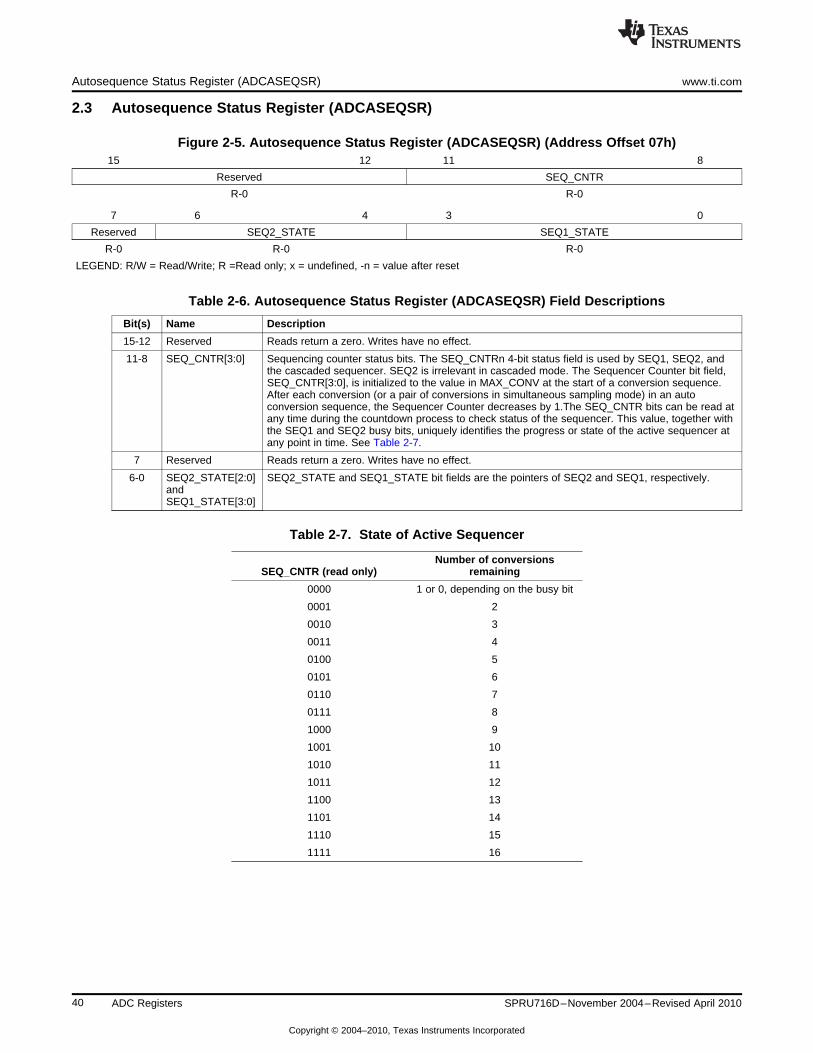
Autosequence Status Register (ADCASEQSR) www.ti.com
2.3 Autosequence Status Register (ADCASEQSR)
Figure 2-5. Autosequence Status Register (ADCASEQSR) (Address Offset 07h)15 12 11 8
Reserved SEQ_CNTR
R-0 R-0
7 6 4 3 0
Reserved SEQ2_STATE SEQ1_STATE
R-0 R-0 R-0
LEGEND: R/W = Read/Write; R =Read only; x = undefined, -n = value after reset
Table 2-6. Autosequence Status Register (ADCASEQSR) Field Descriptions
Bit(s) Name Description
15-12 Reserved Reads return a zero. Writes have no effect.
11-8 SEQ_CNTR[3:0] Sequencing counter status bits. The SEQ_CNTRn 4-bit status field is used by SEQ1, SEQ2, andthe cascaded sequencer. SEQ2 is irrelevant in cascaded mode. The Sequencer Counter bit field,SEQ_CNTR[3:0], is initialized to the value in MAX_CONV at the start of a conversion sequence.After each conversion (or a pair of conversions in simultaneous sampling mode) in an autoconversion sequence, the Sequencer Counter decreases by 1.The SEQ_CNTR bits can be read atany time during the countdown process to check status of the sequencer. This value, together withthe SEQ1 and SEQ2 busy bits, uniquely identifies the progress or state of the active sequencer atany point in time. See Table 2-7.
7 Reserved Reads return a zero. Writes have no effect.
6-0 SEQ2_STATE[2:0] SEQ2_STATE and SEQ1_STATE bit fields are the pointers of SEQ2 and SEQ1, respectively.andSEQ1_STATE[3:0]
Table 2-7. State of Active Sequencer
Number of conversionsSEQ_CNTR (read only) remaining
0000 1 or 0, depending on the busy bit
0001 2
0010 3
0011 4
0100 5
0101 6
0110 7
0111 8
1000 9
1001 10
1010 11
1011 12
1100 13
1101 14
1110 15
1111 16
40 ADC Registers SPRU716D–November 2004–Revised April 2010
Copyright © 2004–2010, Texas Instruments Incorporated
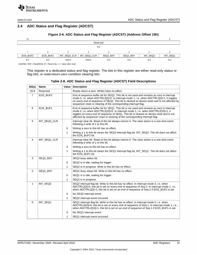
www.ti.com ADC Status and Flag Register (ADCST)
2.4 ADC Status and Flag Register (ADCST)
Figure 2-6. ADC Status and Flag Register (ADCST) (Address Offset 19h)15 8
Reserved
R-0
7 6 5 4 3 2 1 0
EOS_BUF2 EOS_BUF1 INT_SEQ2_CLR INT_SEQ1_CLR SEQ2_BSY SEQ1_BSY INT_SEQ2 INT_SEQ1
R-0 R-0 R/W-0 R/W-0 R-0 R-0 R-0 R-0
LEGEND: R/W = Read/Write; R = Read only; -n = value after reset
This register is a dedicated status and flag register. The bits in this register are either read-only status orflag bits, or read-return-zero condition clearing bits.
Table 2-8. ADC Status and Flag Register (ADCST) Field Descriptions
Bit(s) Name Value Description
15-8 Reserved Reads return a zero. Writes have no effect.
7 EOS_BUF2 End of sequence buffer bit for SEQ2. This bit is not used and remains as zero in interruptmode 0, i.e. when ADCTRL2[2]=0. In interrupt mode 1, i.e. when ADCTRL2[2]=1, it toggleson every end of sequence of SEQ2. This bit is cleared on device reset and is not affected bysequencer reset or clearing of the corresponding interrupt flag.
6 EOS_BUF1 End of sequence buffer bit for SEQ1. This bit is not used and remains as zero in interruptmode 0, i.e. when ADCTRL2[10]=0. In interrupt mode 1, i.e. when ADCTRL2[10]=1, ittoggles on every end of sequence of SEQ1. This bit is cleared on device reset and is notaffected by sequencer reset or clearing of the corresponding interrupt flag.
5 INT_SEQ2_CLR Interrupt clear bit. Read of this bit always returns 0. The clear action is a one-shot eventfollowing a write of 1 to this bit.
0 Writing a zero to this bit has no effect.
1 Writing a 1 to this bit clears the SEQ2 interrupt flag bit, INT_SEQ2. This bit does not affectthe EOS_BUF2 bit.
4 INT_SEQ1_CLR Interrupt clear bit. Read of this bit always returns 0. The clear action is a one-shot eventfollowing a write of 1 to this bit.
0 Writing a zero to this bit has no effect.
1 Writing a 1 to this bit clears the SEQ1 interrupt flag bit, INT_SEQ1. This bit does not affectthe EOS_BUF1 bit.
3 SEQ2_BSY SEQ2 busy status bit.
0 SEQ2 is in idle, waiting for trigger.
1 SEQ2 is in progress. Write to this bit has no effect.
2 SEQ1_BSY SEQ1 busy status bit. Write to this bit has no effect.
0 SEQ1 is in idle, waiting for trigger.
1 SEQ1 is in progress.
1 INT_SEQ2 SEQ2 interrupt flag bit. Write to this bit has no effect. In interrupt mode 0, i.e. whenADCTRL2[2]=0, this bit is set on every end of sequence of Seq 2. In interrupt mode 1, i.e.,when ADCTRL2[2]=1, this bit is set on an end of sequence of Seq 2 if EOS_BUF2 is set.
0 No SEQ2 interrupt event.
1 SEQ2 interrupt event occurred.
0 INT_SEQ1 SEQ1 interrupt flag bit. Write to this bit has no effect. In interrupt mode 0, i.e. whenADCTRL2[10]=0, this bit is set on every end of sequence of Seq 1. In interrupt mode 1, i.e.,when ADCTRL2[10]=1, this bit is set on an end of sequence of Seq 1 if EOS_BUF1 is set.
0 No SEQ1 interrupt event.
1 SEQ1 interrupt event occurred.
41SPRU716D–November 2004–Revised April 2010 ADC Registers
Copyright © 2004–2010, Texas Instruments Incorporated
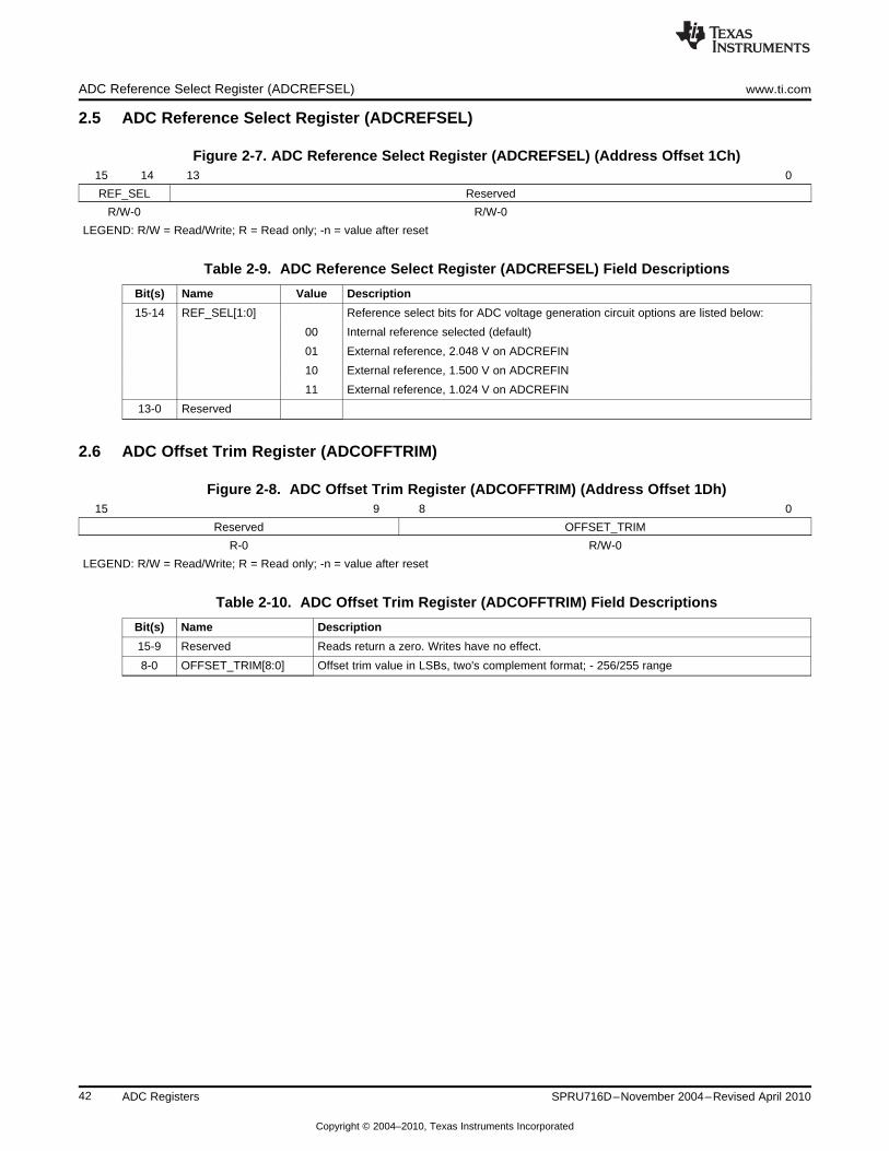
ADC Reference Select Register (ADCREFSEL) www.ti.com
2.5 ADC Reference Select Register (ADCREFSEL)
Figure 2-7. ADC Reference Select Register (ADCREFSEL) (Address Offset 1Ch)15 14 13 0
REF_SEL Reserved
R/W-0 R/W-0
LEGEND: R/W = Read/Write; R = Read only; -n = value after reset
Table 2-9. ADC Reference Select Register (ADCREFSEL) Field Descriptions
Bit(s) Name Value Description
15-14 REF_SEL[1:0] Reference select bits for ADC voltage generation circuit options are listed below:
00 Internal reference selected (default)
01 External reference, 2.048 V on ADCREFIN
10 External reference, 1.500 V on ADCREFIN
11 External reference, 1.024 V on ADCREFIN
13-0 Reserved
2.6 ADC Offset Trim Register (ADCOFFTRIM)
Figure 2-8. ADC Offset Trim Register (ADCOFFTRIM) (Address Offset 1Dh)15 9 8 0
Reserved OFFSET_TRIM
R-0 R/W-0
LEGEND: R/W = Read/Write; R = Read only; -n = value after reset
Table 2-10. ADC Offset Trim Register (ADCOFFTRIM) Field Descriptions
Bit(s) Name Description
15-9 Reserved Reads return a zero. Writes have no effect.
8-0 OFFSET_TRIM[8:0] Offset trim value in LSBs, two's complement format; - 256/255 range
42 ADC Registers SPRU716D–November 2004–Revised April 2010
Copyright © 2004–2010, Texas Instruments Incorporated
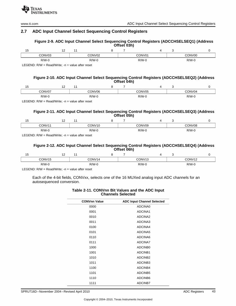
www.ti.com ADC Input Channel Select Sequencing Control Registers
2.7 ADC Input Channel Select Sequencing Control Registers
Figure 2-9. ADC Input Channel Select Sequencing Control Registers (ADCCHSELSEQ1) (AddressOffset 03h)
15 12 11 8 7 4 3 0
CONV03 CONV02 CONV01 CONV00
R/W-0 R/W-0 R/W-0 R/W-0
LEGEND: R/W = Read/Write; -n = value after reset
Figure 2-10. ADC Input Channel Select Sequencing Control Registers (ADCCHSELSEQ2) (AddressOffset 04h)
15 12 11 8 7 4 3 0
CONV07 CONV06 CONV05 CONV04
R/W-0 R/W-0 R/W-0 R/W-0
LEGEND: R/W = Read/Write; -n = value after reset
Figure 2-11. ADC Input Channel Select Sequencing Control Registers (ADCCHSELSEQ3) (AddressOffset 05h)
15 12 11 8 7 4 3 0
CONV11 CONV10 CONV09 CONV08
R/W-0 R/W-0 R/W-0 R/W-0
LEGEND: R/W = Read/Write; -n = value after reset
Figure 2-12. ADC Input Channel Select Sequencing Control Registers (ADCCHSELSEQ4) (AddressOffset 06h)
15 12 11 8 7 4 3 0
CONV15 CONV14 CONV13 CONV12
R/W-0 R/W-0 R/W-0 R/W-0
LEGEND: R/W = Read/Write; -n = value after reset
Each of the 4-bit fields, CONVxx, selects one of the 16 MUXed analog input ADC channels for anautosequenced conversion.
Table 2-11. CONVnn Bit Values and the ADC InputChannels Selected
CONVnn Value ADC Input Channel Selected
0000 ADCINA0
0001 ADCINA1
0010 ADCINA2
0011 ADCINA3
0100 ADCINA4
0101 ADCINA5
0110 ADCINA6
0111 ADCINA7
1000 ADCINB0
1001 ADCINB1
1010 ADCINB2
1011 ADCINB3
1100 ADCINB4
1101 ADCINB5
1110 ADCINB6
1111 ADCINB7
43SPRU716D–November 2004–Revised April 2010 ADC Registers
Copyright © 2004–2010, Texas Instruments Incorporated

ADC Conversion Result Buffer Registers (ADCRESULTn) www.ti.com
2.8 ADC Conversion Result Buffer Registers (ADCRESULTn)
In the cascaded sequencer mode, registers ADCRESULT8 through ADCRESULT15 holds the results ofthe ninth through sixteenth conversions. The ADCRESULTn registers are left justified when read fromPeripheral Frame 2 (0x7108-0x7117) with two wait states and right justified when read from PeripheralFrame 0 (0x0B00-0x0B0F) with zero wait states.
Figure 2-13. ADC Conversion Result Buffer Registers (ADCRESULTn) - (Addresses 0x7108-0x7117)15 14 13 12 11 10 9 8
D11 D10 D9 D8 D7 D6 D5 D4
R-0 R-0 R-0 R-0 R-0 R-0 R-0 R-0
7 6 5 4 3 0
D3 D2 D1 D0 Reserved
R-0 R-0 R-0 R-0 R-0
LEGEND: R/W = Read/Write; R = Read only; -n = value after reset
Figure 2-14. ADC Conversion Result Buffer Registers (ADCRESULTn) - (Addresses0x0B00-0x0B0F)
15 12 11 10 9 8
Reserved D11 D10 D9 D8
R-0 R-0 R-0 R-0 R-0
7 6 5 4 3 2 1 0
D7 D6 D5 D4 D3 D2 D1 D0
R-0 R-0 R-0 R-0 R-0 R-0 R-0 R-0
LEGEND: R/W = Read/Write; R = Read only; -n = value after reset
44 ADC Registers SPRU716D–November 2004–Revised April 2010
Copyright © 2004–2010, Texas Instruments Incorporated

Appendix ASPRU716D–November 2004–Revised April 2010
Revision History
This document was revised to include the following technical change(s). This appendix lists only revisionsmade in the most recent version.
Table A-1. Changes in this Revision
Location Additions/Modifications/Deletions
Delete Section 1.8(ADC Calibration) and 1.11(ADC to DMA Interface)
45SPRU716D–November 2004–Revised April 2010 Revision History
Copyright © 2004–2010, Texas Instruments Incorporated

IMPORTANT NOTICE
Texas Instruments Incorporated and its subsidiaries (TI) reserve the right to make corrections, modifications, enhancements, improvements,and other changes to its products and services at any time and to discontinue any product or service without notice. Customers shouldobtain the latest relevant information before placing orders and should verify that such information is current and complete. All products aresold subject to TI’s terms and conditions of sale supplied at the time of order acknowledgment.
TI warrants performance of its hardware products to the specifications applicable at the time of sale in accordance with TI’s standardwarranty. Testing and other quality control techniques are used to the extent TI deems necessary to support this warranty. Except wheremandated by government requirements, testing of all parameters of each product is not necessarily performed.
TI assumes no liability for applications assistance or customer product design. Customers are responsible for their products andapplications using TI components. To minimize the risks associated with customer products and applications, customers should provideadequate design and operating safeguards.
TI does not warrant or represent that any license, either express or implied, is granted under any TI patent right, copyright, mask work right,or other TI intellectual property right relating to any combination, machine, or process in which TI products or services are used. Informationpublished by TI regarding third-party products or services does not constitute a license from TI to use such products or services or awarranty or endorsement thereof. Use of such information may require a license from a third party under the patents or other intellectualproperty of the third party, or a license from TI under the patents or other intellectual property of TI.
Reproduction of TI information in TI data books or data sheets is permissible only if reproduction is without alteration and is accompaniedby all associated warranties, conditions, limitations, and notices. Reproduction of this information with alteration is an unfair and deceptivebusiness practice. TI is not responsible or liable for such altered documentation. Information of third parties may be subject to additionalrestrictions.
Resale of TI products or services with statements different from or beyond the parameters stated by TI for that product or service voids allexpress and any implied warranties for the associated TI product or service and is an unfair and deceptive business practice. TI is notresponsible or liable for any such statements.
TI products are not authorized for use in safety-critical applications (such as life support) where a failure of the TI product would reasonablybe expected to cause severe personal injury or death, unless officers of the parties have executed an agreement specifically governingsuch use. Buyers represent that they have all necessary expertise in the safety and regulatory ramifications of their applications, andacknowledge and agree that they are solely responsible for all legal, regulatory and safety-related requirements concerning their productsand any use of TI products in such safety-critical applications, notwithstanding any applications-related information or support that may beprovided by TI. Further, Buyers must fully indemnify TI and its representatives against any damages arising out of the use of TI products insuch safety-critical applications.
TI products are neither designed nor intended for use in military/aerospace applications or environments unless the TI products arespecifically designated by TI as military-grade or "enhanced plastic." Only products designated by TI as military-grade meet militaryspecifications. Buyers acknowledge and agree that any such use of TI products which TI has not designated as military-grade is solely atthe Buyer's risk, and that they are solely responsible for compliance with all legal and regulatory requirements in connection with such use.
TI products are neither designed nor intended for use in automotive applications or environments unless the specific TI products aredesignated by TI as compliant with ISO/TS 16949 requirements. Buyers acknowledge and agree that, if they use any non-designatedproducts in automotive applications, TI will not be responsible for any failure to meet such requirements.
Following are URLs where you can obtain information on other Texas Instruments products and application solutions:
Products Applications
Amplifiers amplifier.ti.com Audio www.ti.com/audio
Data Converters dataconverter.ti.com Automotive www.ti.com/automotive
DLP® Products www.dlp.com Communications and www.ti.com/communicationsTelecom
DSP dsp.ti.com Computers and www.ti.com/computersPeripherals
Clocks and Timers www.ti.com/clocks Consumer Electronics www.ti.com/consumer-apps
Interface interface.ti.com Energy www.ti.com/energy
Logic logic.ti.com Industrial www.ti.com/industrial
Power Mgmt power.ti.com Medical www.ti.com/medical
Microcontrollers microcontroller.ti.com Security www.ti.com/security
RFID www.ti-rfid.com Space, Avionics & www.ti.com/space-avionics-defenseDefense
RF/IF and ZigBee® Solutions www.ti.com/lprf Video and Imaging www.ti.com/video
Wireless www.ti.com/wireless-apps
Mailing Address: Texas Instruments, Post Office Box 655303, Dallas, Texas 75265Copyright © 2010, Texas Instruments Incorporated