TMS320DM368 Digital Media System-on-Chip - Texas Instruments
208
TMS320DM368 www.ti.com SPRS668C – APRIL 2010 – REVISED JUNE 2011 TMS320DM368 Digital Media System-on-Chip (DMSoC) Check for Samples: TMS320DM368 1 TMS320DM368 Digital Media System-on-Chip (DMSoC) 1.1 Features 12 device • Highlights • ARM926EJ-S™ Core – High-Performance Digital Media System-on-Chip (DMSoC) – Support for 32-Bit and 16-Bit (Thumb® Mode) Instruction Sets – 432-MHz ARM926EJ-S Clock Rate – DSP Instruction Extensions and Single Cycle – Two Video Image Co-processors MAC (HDVICP, MJCP) Engines – ARM® Jazelle® Technology – Supports a Range of Encode, Decode, and Video Quality Operations – Embedded ICE-RT Logic for Real-Time Debug – Video Processing Subsystem • ARM9 Memory Architecture • HW Face Detect Engine – 16K-Byte Instruction Cache • Resize Engine from 1/16x to 8x – 8K-Byte Data Cache • 16-Bit Parallel AFE (Analog Front-End) Interface Up to 120 MHz – 32K-Byte RAM • 4:2:2 (8-/16-bit) Interface – 16K-Byte ROM • 8-/16-bit YCC and Up to 24-Bit RGB888 – Little Endian Digital Output • Two Video Image Co-processors • 3 DACs for HD Analog Video Output (HDVICP, MJCP) Engines • Hardware On-Screen Display (OSD) – Support a Range of Encode and Decode Operations – Capable of 1080p 30fps H.264 video processing – H.264, MPEG4, MPEG2, MJPEG, JPEG, WMV9/VC1 – Peripherals include EMAC, USB 2.0 OTG, DDR2/NAND, 5 SPIs, 2 UARTs, 2 • Video Processing Subsystem MMC/SD/SDIO, Key Scan – Front End Provides: – 8 Different Boot Modes and Configurable • HW Face Detect Engine Power-Saving Modes • Hardware IPIPE for Real-Time Image – Pin-to-pin and software compatible with Processing DM365 – Resize Engine – Extended temperature (-40ºC – 85ºC) – Resize Images From 1/16x to 8x available – Separate Horizontal/Vertical – 3.3-V and 1.8-V I/O, 1.35-V Core Control – 338-Pin Ball Grid Array at 65nm Process – Two Simultaneous Output Paths Technology • IPIPE Interface (IPIPEIF) • High-Performance Digital Media • Image Sensor Interface (ISIF) and CMOS System-on-Chip (DMSoC) Imager Interface – 432-MHz ARM926EJ-S Clock Rate • 16-Bit Parallel AFE (Analog Front End) – 4:2:2 (8-/16-Bit) Interface Interface Up to 120 MHz – Capable of 1080p 30fps H.264 video • Glueless Interface to Common Video processing Decoders – Pin compatible with DM365 processors • BT.601/BT.656/BT.1120 Digital YCbCr – Fully Software-Compatible With ARM9™ 4:2:2 (8-/16-Bit) Interface – Extended temperature available for 432-MHz • Histogram Module 1 Please be aware that an important notice concerning availability, standard warranty, and use in critical applications of Texas Instruments semiconductor products and disclaimers thereto appears at the end of this data sheet. 2All trademarks are the property of their respective owners. PRODUCTION DATA information is current as of publication date. Copyright © 2010–2011, Texas Instruments Incorporated Products conform to specifications per the terms of the Texas Instruments standard warranty. Production processing does not necessarily include testing of all parameters.
Transcript of TMS320DM368 Digital Media System-on-Chip - Texas Instruments

TMS320DM368
www.ti.com SPRS668C–APRIL 2010–REVISED JUNE 2011
TMS320DM368Digital Media System-on-Chip (DMSoC)
Check for Samples: TMS320DM368
1 TMS320DM368 Digital Media System-on-Chip (DMSoC)
1.1 Features12
device• Highlights• ARM926EJ-S™ Core– High-Performance Digital Media
System-on-Chip (DMSoC) – Support for 32-Bit and 16-Bit(Thumb® Mode) Instruction Sets– 432-MHz ARM926EJ-S Clock Rate
– DSP Instruction Extensions and Single Cycle– Two Video Image Co-processorsMAC(HDVICP, MJCP) Engines
– ARM® Jazelle® Technology– Supports a Range of Encode, Decode, andVideo Quality Operations – Embedded ICE-RT Logic for Real-Time
Debug– Video Processing Subsystem• ARM9 Memory Architecture• HW Face Detect Engine
– 16K-Byte Instruction Cache• Resize Engine from 1/16x to 8x– 8K-Byte Data Cache• 16-Bit Parallel AFE (Analog Front-End)
Interface Up to 120 MHz – 32K-Byte RAM• 4:2:2 (8-/16-bit) Interface – 16K-Byte ROM• 8-/16-bit YCC and Up to 24-Bit RGB888 – Little Endian
Digital Output • Two Video Image Co-processors• 3 DACs for HD Analog Video Output (HDVICP, MJCP) Engines• Hardware On-Screen Display (OSD) – Support a Range of Encode and Decode
Operations– Capable of 1080p 30fps H.264 videoprocessing – H.264, MPEG4, MPEG2, MJPEG, JPEG,
WMV9/VC1– Peripherals include EMAC, USB 2.0 OTG,DDR2/NAND, 5 SPIs, 2 UARTs, 2 • Video Processing SubsystemMMC/SD/SDIO, Key Scan – Front End Provides:
– 8 Different Boot Modes and Configurable • HW Face Detect EnginePower-Saving Modes • Hardware IPIPE for Real-Time Image
– Pin-to-pin and software compatible with ProcessingDM365 – Resize Engine
– Extended temperature (-40ºC – 85ºC) – Resize Images From 1/16x to 8xavailable – Separate Horizontal/Vertical
– 3.3-V and 1.8-V I/O, 1.35-V Core Control– 338-Pin Ball Grid Array at 65nm Process – Two Simultaneous Output Paths
Technology • IPIPE Interface (IPIPEIF)• High-Performance Digital Media • Image Sensor Interface (ISIF) and CMOSSystem-on-Chip (DMSoC) Imager Interface
– 432-MHz ARM926EJ-S Clock Rate • 16-Bit Parallel AFE (Analog Front End)– 4:2:2 (8-/16-Bit) Interface Interface Up to 120 MHz– Capable of 1080p 30fps H.264 video • Glueless Interface to Common Video
processing Decoders– Pin compatible with DM365 processors • BT.601/BT.656/BT.1120 Digital YCbCr– Fully Software-Compatible With ARM9™ 4:2:2 (8-/16-Bit) Interface– Extended temperature available for 432-MHz • Histogram Module
1
Please be aware that an important notice concerning availability, standard warranty, and use in critical applications of TexasInstruments semiconductor products and disclaimers thereto appears at the end of this data sheet.
2All trademarks are the property of their respective owners.
PRODUCTION DATA information is current as of publication date. Copyright © 2010–2011, Texas Instruments IncorporatedProducts conform to specifications per the terms of the TexasInstruments standard warranty. Production processing does notnecessarily include testing of all parameters.

TMS320DM368
SPRS668C–APRIL 2010–REVISED JUNE 2011 www.ti.com
• Lens distortion correction module (LDC) configurable as two 32-bit timers)– Back End Provides: • One 64-Bit Watch Dog Timer
• Hardware On-Screen Display (OSD) • Two UARTs (One fast UART with RTS and CTSFlow Control)• Composite NTSC/PAL video encoder
output • Five Serial Port Interfaces (SPI) each with twoChip-Selects• 8-/16-bit YCC and Up to 24-Bit RGB888
Digital Output • One Master/Slave Inter-Integrated Circuit(I2C) Bus™• 3 DACs for HD Analog Video Output
• One Multi-Channel Buffered Serial Port• LCD Controller(McBSP)• BT.601/BT.656 Digital YCbCr 4:2:2– I2S(8-/16-Bit) Interface– AC97 Audio Codec Interface• Analog-to-Digital Convertor (ADC)– S/PDIF via Software• Power Management and Real Time Clock
Subsystem (PRTCSS) – Standard Voice Codec Interface (AIC12)– Real Time Clock – SPI Protocol (Master Mode Only)
• 16-Bit Host-Port Interface (HPI) – Direct Interface to T1/E1 Framers• 10/100 Mb/s Ethernet Media Access Controller – Time Division Multiplexed Mode (TDM)
(EMAC) - Digital Media – 128 Channel Mode– IEEE 802.3 Compliant • Four Pulse Width Modulator (PWM) Outputs– Supports Media Independent Interface (MII) • Four RTO (Real Time Out) Outputs– Management Data I/O (MDIO) Module • Up to 104 General-Purpose I/O (GPIO) Pins
• Key Scan (Multiplexed with Other Device Functions)• Voice Codec • Boot Modes• External Memory Interfaces (EMIFs) – On-Chip ARM ROM Bootloader (RBL) to Boot
From NAND Flash, MMC/SD, UART, USB,– DDR2 and mDDR SDRAM 16-bit wide EMIFSPI, EMAC, or HPIWith 256 MByte Address Space (1.8-V I/O)
– AEMIF (NOR and OneNAND)– Asynchronous16-/8-bit Wide EMIF (AEMIF)• Configurable Power-Saving Modes• Flash Memory Interfaces• Crystal or External Clock Input (typically– NAND (8-/16-bit Wide Data)
19.2 MHz, 24 MHz, 27 MHz or 36 MHz)– 16 MB NOR Flash, SRAM• Flexible PLL Clock Generators– OneNAND(16-bit Wide Data)• Debug Interface Support• Flash Card Interfaces
– IEEE-1149.1 (JTAG™)– Two Multimedia Card (MMC) / Secure DigitalBoundary-Scan-Compatible(SD/SDIO)
– ETB (Embedded Trace Buffer) with 4K-Bytes– SmartMedia/xDTrace Buffer memory• Enhanced Direct-Memory-Access (EDMA)
– Device Revision ID Readable by ARMController (64 Independent Channels)• 338-Pin Ball Grid Array (BGA) Package• USB Port with Integrated 2.0 High-Speed PHY
(ZCE Suffix), 0.65-mm Ball Pitchthat Supports• 65nm Process Technology– USB 2.0 High-Speed Device• 3.3-V and 1.8-V I/O, 1.35-V Internal– USB 2.0 High-Speed Host (mini-host,• Community Resourcessupporting one external device)
– TI E2E Community– USB On The Go (HS-USB OTG)– TI Embedded Processors Wiki• Four 64-Bit General-Purpose Timers (each
2 TMS320DM368 Digital Media System-on-Chip (DMSoC) Copyright © 2010–2011, Texas Instruments Incorporated
Submit Documentation FeedbackProduct Folder Link(s): TMS320DM368

TMS320DM368
www.ti.com SPRS668C–APRIL 2010–REVISED JUNE 2011
1.2 Description
Developers can now deliver crystal clear multi-format video at up to 1080p H.264 at 30fps (encode andclosed-looped decode) in their digital video designs without concerns of video format support, constrainednetwork bandwidth, limited system storage capacity or cost with the new TMS320DM368 DaVinci™ videoprocessors from Texas Instruments Incorporated (TI).
The DM368 is capable of achieving HD video processing at 1080p 30fps H.264 and is completelypin-to-pin compatible with the DM365 processors, using the same ARM926EJ-S core running at 432 MHz.This ARM9-based DM368 device supports production-qualified H.264BP/MP/HP, MPEG-4, MPEG-2,MJPEG and VC1/WMV9 codecs providing customers with the flexibility to select the right video codec fortheir application. These codecs run on independent coprocessors (HDVICP and MJCP) offloading allcompression needs from the main ARM core. This allows developers to obtain optimal performance fromthe ARM for their applications, including their multi-channel, multi-stream and multi-format needs.
Video surveillance designers achieve greater compression efficiency to provide more storage withoutstraining the network bandwidth. Developers of media playback and camera-driven applications, such asvideo doorbells, digital signage, digital video recorders, portable media players and more can takeadvantage of the low power consumption and can ensure interoperability, as well as product scalability bytaking advantage of the full suite of codecs supported on the DM368.
Along with multi-format HD video, the DM368 also features a suite of peripherals saving developers onsystem cost and complexity to enable a seamless interface to most additional external devices requiredfor video applications. The image sensor interface is flexible enough to support CCD, CMOS, and variousother interfaces such as BT.656, BT1120. The DM368 also offers a high level of integration with HDdisplay support, including three built-in 10-bit HD analog video digital-to-analog converters (DACs),DDR2/mDDR, Ethernet MAC, USB 2.0, integrated audio, host port interface (HPI), analog-to digitalconverter and many more features saving developers on overall system costs, as well as real estate ontheir circuit boards allowing for a slimmer, sleeker design.
Copyright © 2010–2011, Texas Instruments Incorporated TMS320DM368 Digital Media System-on-Chip (DMSoC) 3Submit Documentation Feedback
Product Folder Link(s): TMS320DM368

Lens DistFace Det
IPIPEResizer
ISIF
Video FE
3ChDAC Video
EncoderOSD
Video BE
Bu
ffer
SDTV/HDTVAnalog Video
DigitalRGB/YUV
CameraAFE
VPSS
DDR2Controller
EDMA
NAND/SMMemory
I/F
HPI
16-BitDDR2/mDDR
NAND/OneNAND/NOR Flash,
SmartMedia/xD
Host CPU
16 Bit
8/16 Bit
16 Bit
USB2.0 HS w/OTG
MMC/SD (x2)
SPI (x5)
UART (x2)
I2C
Timer (x4-64b)
WDT (x1-64b)
GIO
PWM (x4)
RTO
McBSP
EMAC
ADC
Key Scan
Voice Codec
SystemI/O
Interface
I-Cache16 KB
D-Cache8 KB
RAM32 KB
ROM16 KB
ARM926EJ-S
ARM INTC
PRTCSSCLOCK CtrlPLL
JTAGI/F
HDVICP MJCP
DMA/Data and Configuration Bus
19.2 MHz, 24 MHz27 MHz or 36 MHz
32.768kHz
PMIC/SW
TMS320DM368
SPRS668C–APRIL 2010–REVISED JUNE 2011 www.ti.com
1.3 Functional Block Diagram
Figure 1-1 shows the functional block diagram of the TMS320DM368 device.
Figure 1-1. Functional Block Diagram
4 TMS320DM368 Digital Media System-on-Chip (DMSoC) Copyright © 2010–2011, Texas Instruments Incorporated
Submit Documentation FeedbackProduct Folder Link(s): TMS320DM368
TMS320DM368
www.ti.com SPRS668C–APRIL 2010–REVISED JUNE 2011
1 TMS320DM368 Digital Media System-on-Chip 6 Peripheral Information and Electrical(DMSoC) ................................................... 1 Specifications .......................................... 76
6.1 Parameter Information Device-Specific Information1.1 Features .............................................. 1...................................................... 76
1.2 Description ........................................... 3 6.2 Recommended Clock and Control Signal Transition1.3 Functional Block Diagram ............................ 4 Behavior ............................................ 77
Revision History (Revision C) ............................. 6 6.3 Power Supplies ..................................... 772 Device Overview ........................................ 7 6.4 Power-Supply Sequencing ......................... 78
6.5 Reset ............................................... 802.1 Device Characteristics ............................... 7
6.6 Oscillators and Clocks .............................. 812.2 Device Compatibility ................................. 86.7 Power Management and Real Time Clock2.3 ARM Subsystem Overview .......................... 8
Subsystem (PRTCSS) .............................. 852.4 System Control Module ............................. 12 6.8 General-Purpose Input/Output (GPIO) ............. 872.5 Power Management ................................ 13 6.9 EDMA Controller .................................... 89
2.6 Memory Map Summary ............................. 14 6.10 External Memory Interface (EMIF) ................. 99
2.7 Pin Assignments .................................... 16 6.11 MMC/SD ........................................... 1206.12 Video Processing Subsystem (VPSS) Overview2.8 Terminal Functions ................................. 21
..................................................... 1232.9 Device Support ..................................... 46
6.13 USB 2.0 ........................................... 1473 Device Configurations ................................ 506.14 Universal Asynchronous Receiver/Transmitter
3.1 System Module Registers .......................... 50 (UART) ............................................ 1553.2 Boot Modes ......................................... 51 6.15 Serial Port Interface (SPI) ......................... 1573.3 Device Clocking .................................... 54 6.16 Inter-Integrated Circuit (I2C) ...................... 167
3.4 Power and Sleep Controller (PSC) ................. 61 6.17 Multi-Channel Buffered Serial Port (McBSP) ..... 170
6.18 Timer .............................................. 1793.5 Pin Multiplexing ..................................... 636.19 Pulse Width Modulator (PWM) .................... 1813.6 Device Reset ....................................... 646.20 Real Time Out (RTO) ............................. 1833.7 Default Device Configurations ...................... 646.21 Ethernet Media Access Controller (EMAC) ....... 1853.8 Debugging Considerations ......................... 696.22 Management Data Input/Output (MDIO) .......... 191
4 System Interconnect .................................. 706.23 Host-Port Interface (HPI) Peripheral .............. 193
5 Device Operating Conditions ....................... 716.24 Key Scan .......................................... 197
5.1 Absolute Maximum Ratings Over Operating Case6.25 Analog-to-Digital Converter (ADC) ................ 199Temperature Range6.26 Voice Codec ....................................... 199(Unless Otherwise Noted) ................................. 716.27 IEEE 1149.1 JTAG ................................ 2015.2 Recommended Operating Conditions .............. 72
7 Mechanical Data ...................................... 2045.3 Electrical Characteristics Over RecommendedRanges of Supply Voltage 7.1 Thermal Data for ZCE ............................. 204and Operating Case Temperature (Unless
7.2 Packaging Information ............................ 204Otherwise Noted) ................................... 74
Copyright © 2010–2011, Texas Instruments Incorporated Contents 5Submit Documentation Feedback
Product Folder Link(s): TMS320DM368

TMS320DM368
SPRS668C–APRIL 2010–REVISED JUNE 2011 www.ti.com
Revision HistoryNOTE: Page numbers for previous revisions may differ from page numbers in the current version.
highlights the technical changes made to the SPRS668B device-specific data sheet to make it aSPRS668C revision.
Revision C UpdatesSee Additions/Changes/Deletions
Global Removed sentence stating "micro-vias are not required."
Figure 2-2 Corrected J5 pin name.
Table 2-5 Changed TYPE of VREF pin from A I/O to A I.
Table 2-5 Changed TYPE of VCOM pin from AI to AO.
Section 3.2.1 Added 24 MHz reference clock to ARM ROM Boot - UART mode.
Table 6-21 Updated first table note.
Table 6-22 Updated second table note.
Table 6-26 Updated table and added table note.
6 Contents Copyright © 2010–2011, Texas Instruments Incorporated
Submit Documentation FeedbackProduct Folder Link(s): TMS320DM368

TMS320DM368
www.ti.com SPRS668C–APRIL 2010–REVISED JUNE 2011
2 Device Overview
2.1 Device Characteristics
Table 2-1 provides an overview of the DMSoC. The table shows significant features of the device,including the peripherals, capacity of on-chip RAM, ARM operating frequency, the package type with pincount, etc.
Table 2-1. Characteristics of the Processor
HARDWARE FEATURES DEVICE
DDR2 / mDDR Memory Controller DDR2 / mDDR (16-bit bus width)
Asynchronous (8/16-bit bus width) RAM,Asynchronous EMIF (AEMIF) Flash (NOR, NAND, OneNAND)
Two MMC/SDFlash Card Interfaces One SmartMedia/xD
64 independent DMA channelsEDMA Eight QDMA channels
Four 64-Bit General Purpose (eachTimers configurable as two separate 32-bit timers)
One 64-Bit Watch Dog
UART Two (one with RTS and CTS flow control)
SPI Five (each supports two slave devices)Peripherals
I2C One (Master/Slave)Not all peripherals pins are 10/100 Ethernet MAC with Management Data I/O Oneavailable at the same time (For
Multi-Channel Buffered Serial Port [McBSP] One McBSPmore detail, see the DeviceConfiguration section). Power Management and Real Time Clock Subsystem RTC (32.768kHz), GPIO(PRTCSS)
Key Scan 4 x 4 Matrix, 5 x 3 Matrix
Voice Codec One
Analog-to-Digital Converter (ADC) 6-channel, 10-bit Interface
General-Purpose Input/Output Port Up to 104
Pulse width modulator (PWM) Four outputs
One Input (VPFE)Configurable Video Ports One Output (VPBE)
High Speed DeviceUSB 2.0 High Speed Host
On The Go (HS-USB-OTG)
Wireless Interfaces Through SDIO
RTO Four Channels
ARMOn-Chip CPU Memory Organization 16-KB I-cache, 8-KB D-cache, 32-KB RAM,
16-KB ROM
See Section 6.27.1, JTAG RegisterJTAG BSDL_ID JTAGID register (address location: 0x01C4 0028) Description(s)
CPU Frequency (Maximum) MHz ARM: 432-MHz
Core (V) 1.35 VVoltage
I/O (V) 3.3 V, 1.8 V
Reference frequency options 19.2 MHz, 24 MHz, 27 MHz, 36 MHzPLL Options Configurable PLL controller PLL bypass, programmable PLL
BGA Package 13 x 13 mm 338-Pin BGA (ZCE)
Process Technology 65 nm
Copyright © 2010–2011, Texas Instruments Incorporated Device Overview 7Submit Documentation Feedback
Product Folder Link(s): TMS320DM368

TMS320DM368
SPRS668C–APRIL 2010–REVISED JUNE 2011 www.ti.com
Table 2-1. Characteristics of the Processor (continued)
HARDWARE FEATURES DEVICE
Product Preview (PP),Product Status (1) Advance Information (AI), PD
or Production Data (PD)
(1) PRODUCTION DATA information is current as of publication date. Products conform to specifications per the terms of TexasInstruments standard warranty. Production processing does not necessarily include testing of all parameters.
2.2 Device Compatibility
The ARM926EJ-S RISC CPU is compatible with other ARM9 CPUs from ARM Holdings plc.
2.3 ARM Subsystem Overview
The ARM Subsystem contains components required to provide the ARM926EJ-S (ARM) master control ofthe overall device system, including the components of the ARM Subsystem, the peripherals, and theexternal memories.
The ARM is responsible for handling system functions such as system-level initialization, configuration,user interface, user command execution, connectivity functions, interface and control of the subsystem,etc. The ARM is master and performs these functions because it has a large program memory space andfast context switching capability, and is thus suitable for complex, multi-tasking, and general-purposecontrol tasks.
2.3.1 Components of the ARM Subsystem
The ARM Subsystem consists of the following components:• ARM926EJ-S RISC processor, including:
– coprocessor 15 (CP15)– MMU– 16KB Instruction cache– 8KB Data cache– Write Buffer– Java accelerator
• ARM Internal Memories– 32KB Internal RAM (32-bit wide access)– 16KB Internal ROM (ARM bootloader for non-AEMIF boot modes)
• Embedded Trace Module and Embedded Trace Buffer (ETM/ETB)• System Control Peripherals
– ARM Interrupt Controller– PLL Controller– Power and Sleep Controller– System Control Module
The ARM also manages/controls all the device peripherals.
Figure 2-1 shows the functional block diagram of the ARM Subsystem.
8 Device Overview Copyright © 2010–2011, Texas Instruments Incorporated
Submit Documentation FeedbackProduct Folder Link(s): TMS320DM368

ARM926EJ-S
16K I$
8K D$ MMU
CP15
Arbiter Arbiter
I-AHB
D-AHB
Master
IFD
MA
Bu
s
I-TCM
D-TCM
16K
RAM0RAM1
16K
ROM
16K
ArbiterSlave
IF
Master IF
CF
G B
us
ARM
Interrupt
Controller
(AINTC)
Control
System
PLLC2
PLLC1
(PSC)
Controller
Sleep
Power
Peripherals...
TMS320DM368
www.ti.com SPRS668C–APRIL 2010–REVISED JUNE 2011
Figure 2-1. ARM Subsystem Block Diagram
2.3.2 ARM926EJ-S RISC CPU
The ARM Subsystem integrates the ARM926EJ-S processor. The ARM926EJ-S processor is a member ofARM9 family of general-purpose microprocessors. This processor is targeted at multi-tasking applicationswhere full memory management, high performance, low die size, and low power are all important. TheARM926EJ-S processor supports the 32-bit ARM and 16 bit THUMB instruction sets, enabling the user totrade off between high performance and high code density. Specifically, the ARM926EJ-S processorsupports the ARMv5TEJ instruction set, which includes features for efficient execution of Java byte codes,providing Java performance similar to Just in Time (JIT) Java interpreter, but without associated codeoverhead.
The ARM926EJ-S processor supports the ARM debug architecture and includes logic to assist in bothhardware and software debug. The ARM926EJ-S processor has a Harvard architecture and provides acomplete high performance subsystem, including:• ARM926EJ -S integer core• CP15 system control coprocessor• Memory Management Unit (MMU)• Separate instruction and data Caches• Write buffer• Separate instruction and data Tightly-Coupled Memories (TCMs) [internal RAM] interfaces• Separate instruction and data AHB bus interfaces• Embedded Trace Module and Embedded Trace Buffer (ETM/ETB)
For more complete details on the ARM9, refer to the ARM926EJ-S Technical Reference Manual, availableat http://www.arm.com
Copyright © 2010–2011, Texas Instruments Incorporated Device Overview 9Submit Documentation Feedback
Product Folder Link(s): TMS320DM368

TMS320DM368
SPRS668C–APRIL 2010–REVISED JUNE 2011 www.ti.com
2.3.3 CP15
The ARM926EJ-S system control coprocessor (CP15) is used to configure and control instruction anddata caches, Tightly-Coupled Memories (TCMs), Memory Management Unit (MMU), and other ARMsubsystem functions. The CP15 registers are programmed using the MRC and MCR ARM instructions,when the ARM in a privileged mode such as supervisor or system mode.
2.3.4 MMU
The ARM926EJ-S MMU provides virtual memory features required by operating systems such as Linux,WindowCE, ultron, ThreadX, etc. A single set of two level page tables stored in main memory is used tocontrol the address translation, permission checks and memory region attributes for both data andinstruction accesses. The MMU uses a single unified Translation Lookaside Buffer (TLB) to cache theinformation held in the page tables. The MMU features are:• Standard ARM architecture v4 and v5 MMU mapping sizes, domains and access protection scheme.• Mapping sizes are:
– 1MB (sections)– 64KB (large pages)– 4KB (small pages)– 1KB (tiny pages)
• Access permissions for large pages and small pages can be specified separately for each quarter ofthe page (subpage permissions)
• Hardware page table walks• Invalidate entire TLB, using CP15 register 8• Invalidate TLB entry, selected by MVA, using CP15 register 8• Lockdown of TLB entries, using CP15 register 10
2.3.5 Caches and Write Buffer
The size of the Instruction Cache is 16KB, Data cache is 8KB. Additionally, the Caches have the followingfeatures:• Virtual index, virtual tag, and addressed using the Modified Virtual Address (MVA)• Four-way set associative, with a cache line length of eight words per line (32-bytes per line) and with
two dirty bits in the Dcache• Dcache supports write-through and write-back (or copy back) cache operation, selected by memory
region using the C and B bits in the MMU translation tables.• Critical-word first cache refilling• Cache lockdown registers enable control over which cache ways are used for allocation on a line fill,
providing a mechanism for both lockdown, and controlling cache corruption• Dcache stores the Physical Address TAG (PA TAG) corresponding to each Dcache entry in the TAG
RAM for use during the cache line write-backs, in addition to the Virtual Address TAG stored in theTAG RAM. This means that the MMU is not involved in Dcache write-back operations, removing thepossibility of TLB misses related to the write-back address.
• Cache maintenance operations provide efficient invalidation of, the entire Dcache or Icache, regions ofthe Dcache or Icache, and regions of virtual memory.
The write buffer is used for all writes to a noncachable bufferable region, write-through region and writemisses to a write-back region. A separate buffer is incorporated in the Dcache for holding write-back forcache line evictions or cleaning of dirty cache lines. The main write buffer has 16-word data buffer and afour-address buffer. The Dcache write-back has eight data word entries and a single address entry.
2.3.6 Tightly Coupled Memory (TCM)
ARM internal RAM is provided for storing real-time and performance-critical code/data and the Interrupt
10 Device Overview Copyright © 2010–2011, Texas Instruments Incorporated
Submit Documentation FeedbackProduct Folder Link(s): TMS320DM368

TMS320DM368
www.ti.com SPRS668C–APRIL 2010–REVISED JUNE 2011
Vector table. ARM internal ROM boot modes include NAND, MMC/SD, UART, USB, SPI, EMAC, and HPI.The RAM and ROM memories interfaced to the ARM926EJ-S via the tightly coupled memory interfacethat provides for separate instruction and data bus connections. Since the ARM TCM does not allowinstructions on the D-TCM bus or data on the I-TCM bus, an arbiter is included so that both data andinstructions can be stored in the internal RAM/ROM. The arbiter also allows accesses to the RAM/ROMfrom extra-ARM sources (e.g., EDMA or other masters). The ARM926EJ-S has built-in DMA support fordirect accesses to the ARM internal memory from a non-ARM master. Because of the time-critical natureof the TCM link to the ARM internal memory, all accesses from non-ARM devices are treated as DMAtransfers.
Instruction and Data accesses are differentiated via accessing different memory map regions, with theinstruction region from 0x0000 through 0x7FFF and data from 0x10000 through 0x17FFF. Placing theinstruction region at 0x0000 is necessary to allow the ARM Interrupt Vector table to be placed at 0x0000,as required by the ARM architecture. The internal 32-KB RAM is split into two physical banks of 16KBeach, which allows simultaneous instruction and data accesses to be accomplished if the code and dataare in separate banks.
2.3.7 Advanced High-performance Bus (AHB)
The ARM Subsystem uses the AHB port of the ARM926EJ-S to connect the ARM to the configuration busand the external memories. Arbiters are employed to arbitrate access to the separate D-AHB and I-AHBby the configuration bus and the external memories bus.
2.3.8 Embedded Trace Macrocell (ETM) and Embedded Trace Buffer (ETB)
To support real-time trace, the ARM926EJ-S processor provides an interface to enable connection of anEmbedded Trace Macrocell (ETM). The ARM926ES-J Subsystem also includes the Embedded TraceBuffer (ETB). The ETM consists of two parts:• Trace Port provides real-time trace capability for the ARM9.• Triggering facilities provide trigger resources, which include address and data comparators, counter,
and sequencers.
The device trace port is not pinned out and is instead only connected to the Embedded Trace Buffer. TheETB has a 4KB buffer memory. ETB enabled debug tools are required to read/interpret the captured tracedata.
2.3.9 ARM Memory Mapping
The ARM memory map is shown in Table 2-3 and Table 2-4. This section describes the memories andinterfaces within the ARM's memory map.
2.3.9.1 ARM Internal Memories
The ARM has access to the following ARM internal memories:• 32KB ARM Internal RAM on TCM interface, logically separated into two 16KB pages to allow
simultaneous access on any given cycle if there are separate accesses for code (I-TCM bus) and data(D-TCM) to the different memory regions.
• 16KB ARM Internal ROM
2.3.9.2 External Memories
The ARM has access to the following External memories:• DDR2 / mDDR Synchronous DRAM• Asynchronous EMIF / OneNAND / NOR• NAND Flash
Copyright © 2010–2011, Texas Instruments Incorporated Device Overview 11Submit Documentation Feedback
Product Folder Link(s): TMS320DM368
TMS320DM368
SPRS668C–APRIL 2010–REVISED JUNE 2011 www.ti.com
• Flash card devices:– MMC/SD– xD– SmartMedia
2.3.10 Peripherals
The ARM has access to all of the peripherals on the device.
2.3.11 ARM Interrupt Controller (AINTC)
The device ARM Interrupt Controller (AINTC) has the following features:• Supports up to 64 interrupt channels (16 external channels)• Interrupt mask for each channel• Each interrupt channel can be mapped to a Fast Interrupt Request (FIQ) or to an Interrupt Request
(IRQ) type of interrupt.• Hardware prioritization of simultaneous interrupts• Configurable interrupt priority (2 levels of FIQ and 6 levels of IRQ)• Configurable interrupt entry table (FIQ and IRQ priority table entry) to reduce interrupt processing time
The ARM core supports two interrupt types: FIQ and IRQ. See the ARM926EJ-S Technical ReferenceManual for detailed information about the ARM’s FIQ and IRQ interrupts. Each interrupt channel ismappable to an FIQ or to an IRQ type of interrupt, and each channel can be enabled or disabled. TheINTC supports user-configurable interrupt-priority and interrupt entry addresses. Entry addresses minimizethe time spent jumping to interrupt service routines (ISRs). When an interrupt occurs, the correspondinghighest priority ISR’s address is stored in the INTC’s ENTRY register. The IRQ or FIQ interrupt routine canread the ENTRY register and jump to the corresponding ISR directly. Thus, the ARM does not require asoftware dispatcher to determine the asserted interrupt.
2.4 System Control Module
The system control module is a system-level module containing status and top-level control logic requiredby the device. The system control module consists of a miscellaneous set of status and control registers,accessible by the ARM and supporting all of the following system features and operations:• Device identification• Device configuration
– Pin multiplexing control– Device boot configuration status
• ARM interrupt and EDMA event multiplexing control• Special peripheral status and control
– Timer64– USB PHY control– VPSS clock and video DAC control and status– DDR VTP control– Clockout circuitry– GIO de-bounce control
• Power management– Deep sleep
• Bandwidth Management– Bus master DMA priority controlFor more information on the System Control Module refer to Section 3, Device Configurations and theTMS320DM36x DMSoC ARM Subsystem Reference Guide (literature number SPRUFG5).
12 Device Overview Copyright © 2010–2011, Texas Instruments Incorporated
Submit Documentation FeedbackProduct Folder Link(s): TMS320DM368

TMS320DM368
www.ti.com SPRS668C–APRIL 2010–REVISED JUNE 2011
2.5 Power Management
The device is designed for minimal power consumption. There are two components to powerconsumption: active power and leakage power. Active power is the power consumed to perform work andscales with clock frequency and the amount of computations being performed. Active power can bereduced by controlling the clocks in such a way as to either operate at a clock setting just high enough tocomplete the required operation in the required time-line or to run at a clock setting until the work iscomplete and then drastically cut the clocks (e.g. to PLL Bypass mode) until additional work must beperformed. Leakage power is due to static current leakage and occurs regardless of the clock rate.Leakage, or standby power, is unavoidable while power is applied and scales roughly with the operatingjunction temperatures. Leakage power can only be avoided by removing power completely from a deviceor subsystem. The device includes several power management modes which are briefly described inTable 2-2. See the TMS320DM36x DMSoC ARM Subsystem Reference Guide (literature numberSPRUFG5) for more information on power management.
Table 2-2. Power Management Conditions
GIO, SPI,POWER MGMT. OTHER DDRCORE OSC. PLL ARM926 UART, PWM,APPLICATION PRTCSS PERIPH. CLOCK/ DESCRIPTIONPOWER POWER CNTRLR. CLOCK I2C TIMERSCENARIO CLOCKS MODECLOCKS CLOCKS
This conditionconsumes the lowestPRTCSS Active Off Off Off Off Off Off Off Off possible power, exceptfor the PRTCSS.
This mode consumesthe second lowestBypass Suspend / possible power, exceptModeDeep Sleep Mode (1) Active On Off Off Off Off Off "Self- for PRTCSS and core(not Refresh" power, where only theActive) deep sleep circuit is onin this mode.
This condition keepsthe minimum possiblemodules powered-on
Suspend / in order to wake up theBypassStandby Active On On Off On Off Off "Self- device. Clocks areMode Refresh" suspended except forGIO (interrupts),UART, and I2C (inslave mode).
Most clocks aresuspended, except forARM, GIO, UART,SPI, I2C, PWM, andSuspend /Low-power Bypass timers. Since ARM willActive On On On On / Off On / Off On / Off "Self-(PLL Bypass Mode) Mode not have access toRefresh" DDR, its internalCache will be eitherfrozen or notaccessed.
The device, includingNominal system PLLs, are on.System Running Active On On PLL Mode On On / Off On / Off On / Off Clock / This condition(PLL Mode) Operation conserves the least
amount of power.
(1) For more details, see TMS320DM36x DMSoC ARM Subsystem Reference Guide (literature number SPRUFG5)
Copyright © 2010–2011, Texas Instruments Incorporated Device Overview 13Submit Documentation Feedback
Product Folder Link(s): TMS320DM368

TMS320DM368
SPRS668C–APRIL 2010–REVISED JUNE 2011 www.ti.com
2.6 Memory Map Summary
Table 2-3 shows the memory map address ranges of the device. Table 2-4 depicts the expanded map ofthe Configuration Space (0x01C0 0000 through 0x01FF FFFF). The device has multiple on-chip memoriesassociated with its processor and various subsystems. To help simplify software development a unifiedmemory map is used where possible to maintain a consistent view of device resources across all busmasters. The bus masters are the ARM, EDMA, EMAC, USB, HPI, MJCP, HDVICP and VPSS. TheMaster Peripherals are EMAC, USB, and HPI. Please refer to Section 4 for more details.
Table 2-3. Memory Map
Start Address End Address Size (Bytes) ARM EDMA Master Periph VPSSMem Map Mem Map Mem Map Mem Map
0x0000 0000 0x0000 3FFF 16K ARM RAM0(Instruction)
0x0000 4000 0x0000 7FFF 16K ARM RAM1 Reserved Reserved(Instruction)
0x0000 8000 0x0000 BFFF 16K ARM ROM(Instruction)
0x0000 C000 0x0000 FFFF 16K Reserved
0x0001 0000 0x0001 3FFF 16K ARM RAM0 (Data) ARM RAM0 ARM RAM0
0x0001 4000 0x0001 7FFF 16K ARM RAM1 (Data) ARM RAM1 ARM RAM1
0x0001 8000 0x0001 BFFF 16K ARM ROM ARM ROM ARM ROM
0x0001 C000 0x000F FFFF 912K Reserved
0x0010 0000 0x01BB FFFF 26M
0x01BC 0000 0x01BC 0FFF 4K ARM ETB Mem
0x01BC 1000 0x01BC 17FF 2K ARM ETB Reg Reserved
0x01BC 1800 0x01BC 18FF 256 ARM IceCrusher Reserved
0x01BC 1900 0x01BC FFFF 59136 Reserved
0x01BD 0000 0x01BF FFFF 192K
0x01C0 0000 0x01FF FFFF 4M CFG Bus CFG Bus CFG BusPeripherals Peripherals Peripherals
0x0200 0000 0x09FF FFFF 128M ASYNC EMIF (Data) ASYNC EMIF (Data)
0x0A00 0000 0x11EF FFFF 127M - 16K Reserved Reserved
0x11F0 0000 0x11F1 FFFF 128K MJCP DMA Port MJCP DMA Port
0x11F2 0000 0x11FF FFFF 896K Reserved Reserved
0x1200 0000 0x1207 FFFF 512K HDVICP DMA Port1 HDVICP DMA Port1 HDVICPDMA Port1
0x1208 0000 0x120F FFFF 512K Reserved HDVICP DMA Port2 Reserved
0x1210 0000 0x1217 FFFF 512K HDVICP DMA Port3
0x1218 0000 0x1FFF FFFF 222.5M Reserved
0x2000 0000 0x2000 7FFF 32K DDR EMIF Control DDR EMIF ControlRegs Regs
0x2000 8000 0x41FF FFFF 544M-32K
0x4200 0000 0x49FF FFFF 128M Reserved Reserved
0x4A00 0000 0x7FFF FFFF 864M
0x8000 0000 0x8FFF FFFF 256M DDR EMIF DDR EMIF DDR EMIF DDR EMIF
0x9000 0000 0xFFFF FFFF 1792M Reserved Reserved Reserved Reserved
14 Device Overview Copyright © 2010–2011, Texas Instruments Incorporated
Submit Documentation FeedbackProduct Folder Link(s): TMS320DM368
TMS320DM368
www.ti.com SPRS668C–APRIL 2010–REVISED JUNE 2011
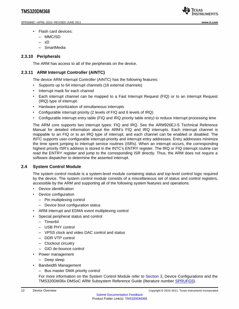
Table 2-4. ARM Configuration Bus Access to Peripherals
Address
Region Start End Size
EDMA CC 0x01C0 0000 0x01C0 FFFF 64K
EDMA TC0 0x01C1 0000 0x01C1 03FF 1K
EDMA TC1 0x01C1 0400 0x01C1 07FF 1K
EDMA TC2 0x01C1 0800 0x01C1 0BFF 1K
EDMA TC3 0x01C1 0C00 0x01C1 0FFF 1K
Reserved 0x01C1 1000 0x01C1 FFFF 60 K
UART0 0x01C2 0000 0x01C2 03FF 1K
Reserved 0x01C2 0400 0x01 20 7FFF 1K
Timer 3 0x01C2 0800 0x01C2 0BFF 1K
Real-time out 0x01C2 0C00 0x01C2 0FFF 1K
I2C 0x01C2 1000 0x01C2 13FF 1K
Timer 0 0x01C2 1400 0x01C2 17FF 1K
Timer 1 0x01C2 1800 0x01C2 1BFF 1K
Timer 2 0x01C2 1C00 0x01C2 1FFF 1K
PWM0 0x01C2 2000 0x01C2 23FF 1K
PWM1 0x01C2 2400 0x01C2 27FF 1K
PWM2 0x01C2 2800 0x01C2 2BFF 1K
PWM3 0x01C2 2C00 0x01C2 2FFF 1K
SPI4 0x01C2 3000 0x01C2 37FF 2K
Timer 4 0x01C2 3800 0x01C2 3BFF 1K
ADCIF 0x01C2 3C00 0x01C2 3FFF 1K
Reserved 0x01C2 4000 0x01C3 4FFF 112K
System Module 0x01C4 0000 0x01C4 07FF 2K
PLL Controller 1 0x01C4 0800 0x01C4 0BFF 1K
PLL Controller 2 0x01C4 0C00 0x01C4 0FFF 1K
Power/Sleep Controller 0x01C4 1000 0x01C4 1FFF 4K
Reserved 0x01C4 2000 0x01C4 7FFF 24K
ARM Interrupt Controller 0x01C4 8000 0x01C4 83FF 1K
Reserved 0x01 C4 8400 0x01C63FFF 111K
USB OTG 2.0 Regs / RAM 0x01C6 4000 0x01C6 5FFF 8K
SPI0 0x01C6 6000 0x01C6 67FF 2K
SPI1 0x01C6 6800 0x01C6 6FFF 2K
GPIO 0x01C6 7000 0x01C6 77FF 2K
SPI2 0x01C6 7800 0x01C6 FFFF 2K
SPI3 0x01C6 8000 0x01C6 87FF 2K
Reserved 0x01C6 8800 0x01C6 87FF 2K
PRTCSS Interface Registers 0x01C6 9000 0x01C6 93FF 1K
KEYSCAN 0x01C6 9400 0x01C6 97FF 1K
HPI 0x01C6 9800 0x01C6 9FFF 2K
Reserved 0x01C6 A000 0x01C6 FFFF 24K
VPSS Subsystem
ISP System Configuration Registers 0x01C7 0000 0x01C7 00FF 256
VPBE Clock Control Register 0x01C7 0200 0x01C7 02FF 256
Resizer Registers 0x01C7 0400 0x01C7 07FF 1K
IPIPE Registers 0x01C7 0800 0x01C7 0FFF 2K
ISIF Registers 0x01C7 1000 0x01C7 11FF 512
Copyright © 2010–2011, Texas Instruments Incorporated Device Overview 15Submit Documentation Feedback
Product Folder Link(s): TMS320DM368

TMS320DM368
SPRS668C–APRIL 2010–REVISED JUNE 2011 www.ti.com
Table 2-4. ARM Configuration Bus Access to Peripherals (continued)
Address
IPIPEIF Registers 0x01C7 1200 0x01C7 12FF 768
Reserved 0x01C7 1400 0x01C7 17FF 768
FDIF Registers 0x01C7 1800 0x01C7 1BFF 1K
OSD Registers 0x01C7 1C00 0x01C7 1CFF 256
Reserved 0x01C7 1D00 0x01C7 1DFF 256
VENC Registers 0x01C7 1E00 0x01C7 1FFF 512
Reserved 0x01C7 2000 0x01CF FFFF 568K
Multimedia / SD 1 0x01D0 0000 0x01D0 1FFF 8K
McBSP 0x01D0 2000 0x01D0 3FFF 8K
Reserved 0x01D0 4000 0x01D0 5FFF 8K
UART1 0x01D0 6000 0x01D0 63FF 1K
Reserved 0x01D0 6400 0x01D0 7FFF 3K
EMAC Control Registers 0x01D0 7000 0x01D0 9FFF 0x01D0 7FFF4K
EMAC Control Module RAM 0x01D0 8000 8K
EMAC Control Module Registers 0x01D0 A000 0x01D0 AFFF 4K
EMAC MDIO Control Registers 0x01D0 B000 0x01D0 B7FF 2K
Voice Codec 0x01D0 C000 0x01D0 C3FF 1K
Reserved 0x01D0 C400 0x01D0 FFFF 17K
ASYNC EMIF Control 0x01D1 0000 0x01D1 0FFF 4K
Multimedia / SD 0 0x01D1 1000 0x01D1 FFFF 60K
Reserved 0x01D2 0000 0x01D3 FFFF 128K
Reserved 0x01D4 0000 0x01DF FFFF 768K
Reserved 0x01E0 0000 0x01FF FFFF 2M
ASYNC EMIF Data (CE0) 0x0200 0000 0x03FF FFFF 32M
ASYNC EMIF Data (CE1) 0x0400 0000 0x05FF FFFF 32M
Reserved 0x0600 0000 0x09FF FFFF 64M
Reserved 0x0A00 0000 0x0FFF FFFF 96M
2.7 Pin Assignments
Extensive use of pin multiplexing is used to accommodate the largest number of peripheral functions inthe smallest possible package. Pin multiplexing is controlled using a combination of hardwareconfiguration at device reset and software programmable register settings.
2.7.1 Pin Map (Bottom View)
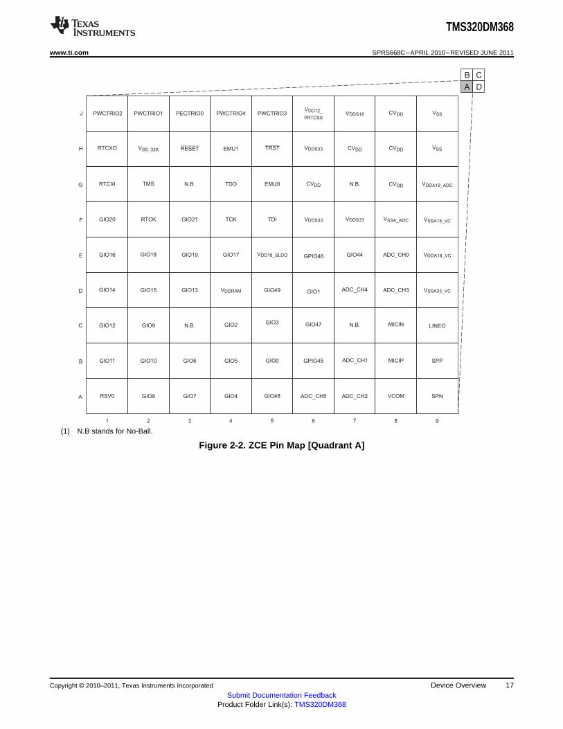
Figure 2-2 through Figure 2-5 show the pin assignments in four quadrants (A, B, C, and D).
16 Device Overview Copyright © 2010–2011, Texas Instruments Incorporated
Submit Documentation FeedbackProduct Folder Link(s): TMS320DM368
9
J
8765431
H
G
VDD12_
PRTCSS
F
E
D
PWCTRIO3
C
B
A
VDDS18PWCTRIO4PECTRIO0
VSSVDDS33EMU1RESETRTCXO
VDDA18_ADCCVDDEMU0N.B.RTCXI
VSSA_ADCVDDS33TDITCKGIO21GIO20
VDDA18_VCADC_CH0GIO44GPIO46VDD18_SLDOGIO17GIO19GIO16
VSSA33_VCADC_CH3GIO1GIO49GIO13GIO14
LINEOMICINN.B.GIO47GIO3GIO2N.B.GIO12
SPPMICIPADC_CH1GPIO45GIO0GIO5GIO6GIO11
SPNVCOMADC_CH2ADC_CH5GIO48GIO4GIO7RSV0
2
PWCTRIO1
VSS_32K
TMS
RTCK
GIO18
GIO15
GIO9
GIO10
GIO8
PWCTRIO2
CVDD
VSSA18_VC
ADC_CH4VDDRAM
VDDS33
TDO N.B.
CVDDCVDDTRST
CVDD VSS
A
B C
D
TMS320DM368
www.ti.com SPRS668C–APRIL 2010–REVISED JUNE 2011
(1) N.B stands for No-Ball.
Figure 2-2. ZCE Pin Map [Quadrant A]
Copyright © 2010–2011, Texas Instruments Incorporated Device Overview 17Submit Documentation Feedback
Product Folder Link(s): TMS320DM368

W
9
DDR_DQ6
8
DDR_DQ8
7654
GIO36
32
GIO32
1
V GIO38GIO34GIO23
UDDR_
DQSN0
T GIO24
R
P
N
M
L
K
DDR_DQ12
DDR_DQM1
GIO41VSS
DDR_DQ5
DDR_DQ11
DDR_DQ14
DDR_DQ15
GIO33GIO28
DDR_DQ9N.B.DDR_
DQSN1GIO40
GIO35
GIO31N.B.GIO29GIO26
DDR_DQGATE1
DDR_DQGATE0
GIO43GIO37GIO27GIO25
DDR_DQ7DDR_DQ10DDR_DQ13GIO42GIO39RSV2VPPGIO22RSV1
VDD18_DDRVSSVDDS33VDDA33_USBVSSA33_USBVSSA18_USBUSB_DM
VDD18_DDRVSSVDDS33VDD18_USBN.B.USB_VBUSUSB_DP
VSSVSSVDDA12LDO_
USBVSSAPWRSTPWRCNTONUSB_ID
VSSVDDMXIPWCTRO1PWCTRO2PWCTRO3VSS_MX1MXI1
VSSCVDDVDD18_PRTCSSPWCTRIO5N.B.PWCTRO0MXO1
VDDS18
PWCTRIO6 VDD12_PRTCSS
VSSVSS
VSS
N.B.VDDA18_PLL
VDDS33
GIO30 DDR_DQS1
CVDD
A
B C
D
TMS320DM368
SPRS668C–APRIL 2010–REVISED JUNE 2011 www.ti.com
(1) N.B stands for No-Ball.
Figure 2-3. ZCE Pin Map [Quadrant B]
18 Device Overview Copyright © 2010–2011, Texas Instruments Incorporated
Submit Documentation FeedbackProduct Folder Link(s): TMS320DM368

VSS
19
W
18
DDR_A11
17
DDR_A8
16
DDR_A6
15
DDR_A2
14
DDR_BA0
13
DDR_WE
12
DDR_CLK
11
DDR_CLK
10
DDR_DQ4
EM_A11 VEM_A13DDR_A12
DDR_A10DDR_A5DDR_A1DDR_BA2DDR_CASDDR_DQ1DDR_DQ3
EM_A10 UEM_A12N.B.DDR_A9DDR_A4DDR_A0N.B.DDR_RASDDR_DQ0N.B.
EM_A8 TEM_A9EM_A7DDR_A7DDR_A3DDR_CSDDR_DQM0
EM_A4 REM_A6EM_BA1EM_A5EM_A3VDD_
AEMIF1_18_33DDR_CKEVDD18_DDR
DDR_PADREFP
DDR_DQ2
EM_D13 PEM_D15EM_BA0EM_D14EM_D12VDD18_DDR
EM_D9 NEM_D10N.B.EM_D8VSSVDD18_DDR
EM_A1 MEM_A2EM_CE[0]EM_ADVEM_CLKVDDS18
EM_D5 LEM_D6EM_A0EM_D7EM_D4VSS
EM_D2 KEM_D0N.B.
DDR_VREF VDD18_DDRVDD_
AEMIF1_18_33
VDDS33 CVDD
VSS CVDD
VDD_
AEMIF2_18_33
EM_D3 EM_D1N.B.VSS
VSS
CVDDCVDDVSSCVDD
EM_D11N.B.VSSN.B.
VSS
DDR_A13DDR_BA1DDR_DQS0
VDD_
AEMIF2_18_33
A
B C
D
TMS320DM368
www.ti.com SPRS668C–APRIL 2010–REVISED JUNE 2011
(1) N.B stands for No-Ball.
Figure 2-4. ZCE Pin Map [Quadrant C]
Copyright © 2010–2011, Texas Instruments Incorporated Device Overview 19Submit Documentation Feedback
Product Folder Link(s): TMS320DM368

19181716151413121110
EM_OE J
MMCSD0_DATA1 H
YOUT6 G
F
E
D
C
VDDS18
B
A
EM_WAITEM_CE[1]MMCSD0_CLKEM_WEVSS
MMCSD0_DATA0
MMCSD0_DATA3
MMCSD0_CMD
VSYNCN.B.HSYNC
YOUT2YOUT4YOUT1YOUT3YOUT5
COUT6COUT7COUT4C_WE_FIELD
VDDA12_DACVSSA18_DAC
VDDA33_VC
COUT2COUT1COUT0YIN0YIN1YIN4VREF
LCD_OEFIELDN.B.CIN2CIN6HDN.B.YIN7COMPPRN.B.
VCLK
CIN1
CIN5
CIN4
CIN0
CIN3
YIN2
CIN7
VD
YIN3
YIN5
YIN6
COMPY
COMPPB
IDACOUT
IREF
VDDS18
CVDD
VDDS33 VDDS18MMCSD0_
DATA2
VSSVDD_ISIF18_33VDD_ISIF18_33VSSA12_DACVDDS33
COUT5
EXTCLKVFB
VSSTVOUT
VDDA18_DAC PCLK COUT3
YOUT0VSS
YOUT7N.B.VSSVSSN.B.
VSS CVDD
CVDDVSSVSS
A
B C
D
TMS320DM368
SPRS668C–APRIL 2010–REVISED JUNE 2011 www.ti.com
(1) N.B stands for No-Ball.
Figure 2-5. ZCE Pin Map [Quadrant D]
20 Device Overview Copyright © 2010–2011, Texas Instruments Incorporated
Submit Documentation FeedbackProduct Folder Link(s): TMS320DM368

TMS320DM368
www.ti.com SPRS668C–APRIL 2010–REVISED JUNE 2011
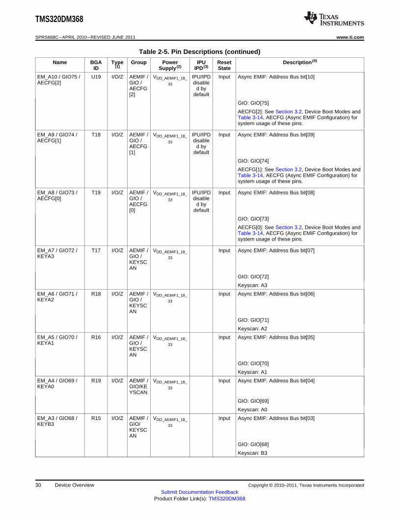
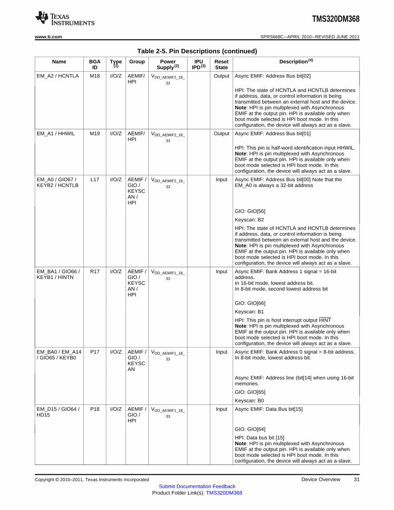
2.8 Terminal Functions
Table 2-5 provides a complete pin description list which shows external signal names, the associated pin(ball) numbers along with the mechanical package designator, the pin type, whether the pin has anyinternal pullup or pulldown resistors, and a functional pin description. For more detailed information ondevice configuration, peripheral selection, multiplexed/shared pins, and debugging considerations, seeSection 3.
Table 2-5. Pin Descriptions
Name BGA Type Group Power IPU Reset Description (4)
ID (1) Supply (2) IPD (3) State
CIN7 (5) A15 I/O ISIF VDD_ISIF18_33 IPD Input Standard ISIF Analog Front End (AFE): raw[7]
YCC 16-bit: time multiplexed between chroma:CB/CR[07]
YCC 08-bit (which allows for 2 simultaneous decoderinputs), it is time multiplexed between luma andchroma of the upper channel. Y/CB/CR[07]
CIN6 (5) C15 I/O ISIF VDD_ISIF18_33 IPD Input Standard ISIF Analog Front End (AFE): raw[6]
YCC 16-bit: time multiplexed between chroma:CB/CR[06]
YCC 08-bit (which allows for 2 simultaneous decoderinputs), it is time multiplexed between luma andchroma of the upper channel. Y/CB/CR[06]
CIN5 (5) B16 I/O ISIF VDD_ISIF18_33 IPD Input Standard ISIF Analog Front End (AFE): raw[5]
YCC 16-bit: time multiplexed between chroma:CB/CR[05]
YCC 08-bit (which allows for 2 simultaneous decoderinputs), it is time multiplexed between luma andchroma of the upper channel. Y/CB/CR[05]
CIN4 (5) A16 I/O ISIF VDD_ISIF18_33 IPD Input Standard ISIF Analog Front End (AFE): raw[4]
YCC 16-bit: time multiplexed between chroma:CB/CR[04]
YCC 08-bit (which allows for 2 simultaneous decoderinputs), it is time multiplexed between luma andchroma of the upper channel. Y/CB/CR[04]
CIN3 (5) A17 I/O ISIF VDD_ISIF18_33 IPD Input Standard ISIF Analog Front End (AFE): raw[3]
YCC 16-bit: time multiplexed between chroma:CB/CR[03]
YCC 08-bit (which allows for 2 simultaneous decoderinputs), it is time multiplexed between luma andchroma of the upper channel. Y/CB/CR[03]
CIN2 (5) C16 I/O ISIF VDD_ISIF18_33 IPD Input Standard ISIF Analog Front End (AFE): raw[2]
YCC 16-bit: time multiplexed between chroma:CB/CR[02]
YCC 08-bit (which allows for 2 simultaneous decoderinputs), it is time multiplexed between luma andchroma of the upper channel. Y/CB/CR[02]
(1) I = Input, O = Output, Z = High impedance, S = Supply voltage, GND = Ground, A = Analog signal.(2) Specifies the operating I/O supply voltage for each signal. See Section 6.3 , Power Supplies for more detail.(3) PD = pull-down, PU = pull-up. (To pull up a signal to the opposite supply rail, a 1 kΩ resistor should be used.)(4) To reduce EMI and reflections, depending on the trace length, approximately 22 Ω to 50 Ω damping resistors are recommend on the
following outputs placed near the device: YOUT(0-7),COUT(0-7), HSYNC,VSYNC,LCD_OE,FIELD, and,VCLK. The trace lengths shouldbe minimized.
(5) The Y input (YIN[7:0]) and C input (CIN[7:0]) buses can be swapped by programming the field bit YCINSWP in the VPFE CCDConfiguration (CCDCFG) register (0x01C7 0136h).IF YCINSWP bit is 0 (default) YIN[7:0] = Y signal / CIN[7:0] = C signal .IF YCINSWP bit is 1 YIN[7:0] = C signal / CIN[7:0] = Y signalFor more information, see the TMS320DM36x Video Processing Front End (VPFE) Reference Guide (literature number SPRUFG8).
Copyright © 2010–2011, Texas Instruments Incorporated Device Overview 21Submit Documentation Feedback
Product Folder Link(s): TMS320DM368

TMS320DM368
SPRS668C–APRIL 2010–REVISED JUNE 2011 www.ti.com
Table 2-5. Pin Descriptions (continued)
Name BGA Type Group Power IPU Reset Description (4)
ID (1) Supply (2) IPD (3) State
CIN1 (5) A18 I/O ISIF VDD_ISIF18_33 IPD Input Standard ISIF Analog Front End (AFE): raw[1]
YCC 16-bit: time multiplexed between chroma:CB/CR[01]
YCC 08-bit (which allows for 2 simultaneous decoderinputs), it is time multiplexed between luma andchroma of the upper channel. Y/CB/CR[01]
CIN0 (5) B17 I/O ISIF VDD_ISIF18_33 IPD Input Standard ISIF Analog Front End (AFE): raw[0]
YCC 16-bit: time multiplexed between chroma:CB/CR[00]
YCC 08-bit (which allows for 2 simultaneous decoderinputs), it is time multiplexed between luma andchroma of the upper channel. Y/CB/CR[00]
YIN7 (5) / GIO103 C12 I/O ISIF/ VDD_ISIF18_33 IPD Input Standard ISIF Analog Front End (AFE): raw[15]/SPI3_SCLK GIO /
SPI3
YCC 16-bit: time multiplexed between luma: Y[07]
YCC 08-bit (which allows for 2 simultaneous decoderinputs), it is time multiplexed between luma andchroma of the lower channel. Y/CB/CR[07]
GIO: GIO[103]
SPI3: Clock
YIN6 (5) / GIO102 A13 I/O ISIF / VDD_ISIF18_33 IPD Input Standard ISIF Analog Front End (AFE): raw[14]/SPI3_SIMO GIO /
SPI3
YCC 16-bit: time multiplexed between luma: Y[06]
YCC 08-bit (which allows for 2 simultaneous decoderinputs), it is time multiplexed between luma andchroma of the lower channel. Y/CB/CR[06]
GIO: GIO[102]
SPI3: Slave Input Master Output Data Signal
YIN5 (6) / GIO101 B13 I/O ISIF / VDD_ISIF18_33 IPD Input Standard ISIF Analog Front End (AFE): raw[13]/SPI3_SCS[0] GIO /
SPI3
YCC 16-bit: time multiplexed between luma: Y[05]
YCC 08-bit (which allows for 2 simultaneous decoderinputs), it is time multiplexed between luma andchroma of the lower channel. Y/CB/CR[05]
GIO: GIO[101]
SPI3: Chip Select 0
YIN4 (6) / GIO100 / D12 I/O ISIF / VDD_ISIF18_33 IPD Input Standard ISIF Analog Front End (AFE): raw[12]SPI3_SOMI / GIO /SPI3_SCS[1] SPI3
YCC 16-bit: time multiplexed between luma: Y[04]
YCC 08-bit (which allows for 2 simultaneous decoderinputs), it is time multiplexed between luma andchroma of the lower channel. Y/CB/CR[04]
GIO: GIO[100]
SPI3: Slave Output Master Input Data Signal
SPI3: Chip Select 1
(6) The Y input (YIN[7:0]) and C input (CIN[7:0]) buses can be swapped by programming the field bit YCINSWP in the VPFE CCDConfiguration (CCDCFG) register (0x01C7 0136h).IF YCINSWP bit is 0 (default) YIN[7:0] = Y signal / CIN[7:0] = C signal .IF YCINSWP bit is 1 YIN[7:0] = C signal / CIN[7:0] = Y signalFor more information, see the TMS320DM36x Video Processing Front End (VPFE) Reference Guide (literature number SPRUFG8).
22 Device Overview Copyright © 2010–2011, Texas Instruments Incorporated
Submit Documentation FeedbackProduct Folder Link(s): TMS320DM368

TMS320DM368
www.ti.com SPRS668C–APRIL 2010–REVISED JUNE 2011
Table 2-5. Pin Descriptions (continued)
Name BGA Type Group Power IPU Reset Description (4)
ID (1) Supply (2) IPD (3) State
YIN3 (6) / GIO99 A14 I/O ISIF / VDD_ISIF18_33 IPD Input Standard ISIF Analog Front End (AFE): raw[11]GIO
YCC 16-bit: time multiplexed between luma: Y[03]
YCC 08-bit (which allows for 2 simultaneous decoderinputs), it is time multiplexed between luma andchroma of the lower channel. Y/CB/CR[03]
GIO: GIO[99]
YIN2 (6) / GIO98 B15 I/O ISIF / VDD_ISIF18_33 IPD Input Standard ISIF Analog Front End (AFE): raw[10]GIO
YCC 16-bit: time multiplexed between luma: Y[02]
YCC 08-bit (which allows for 2 simultaneous decoderinputs), it is time multiplexed between luma andchroma of the lower channel. Y/CB/CR[02]
GIO: GIO[98]
YIN1 (6) / GIO97 D14 I/O ISIF / VDD_ISIF18_33 IPD Input Standard ISIF Analog Front End (AFE): raw[09]GIO
YCC 16-bit: time multiplexed between luma: Y[01]
YCC 08-bit (which allows for 2 simultaneous decoderinputs), it is time multiplexed between luma andchroma of the lower channel. Y/CB/CR[01]
GIO: GIO[97]
YIN0 (7) / GIO96 D15 I/O ISIF / VDD_ISIF18_33 IPD Input Standard ISIF Analog Front End (AFE): raw[08]GIO
YCC 16-bit: time multiplexed between luma: Y[00]
YCC 08-bit (which allows for 2 simultaneous decoderinputs), it is time multiplexed between luma andchroma of the lower channel. Y/CB/CR[00]
GIO: GIO[96]
HD / GIO95 C14 I/O ISIF / VDD_ISIF18_33 IPD Input Horizontal synchronization signal that can be eitherGIO an input (slave mode) or an output (master mode).
Tells the ISIF when a new line starts.
GIO: GIO[95]
VD / GIO94 B14 I/O ISIF / VDD_ISIF18_33 IPD Input Vertical synchronization signal that can be either anGIO input (slave mode) or an output (master mode). Tells
the ISIF when a new frame starts.
GIO: GIO[94]
C_WE_FIELD / E13 I/O ISIF / VDD_ISIF18_33 IPD Input Write enable input signal is used by external deviceGIO93 / CLKOUT0 GIO / (AFE/TG) to gate the DDR output of the ISIF module./ USBDRVVBUS CLKOU
T / USB
Alternately, the field identification input signal is usedby external device (AFE/TG) to indicate the which oftwo frames is input to the ISIF module for sensorswith interlaced output. ISIF handles 1- or 2-fieldsensors in hardware.
GIO: GIO[93]
CLKOUT0: Clock Output
USB: Digital output to control external 5 V supply
PCLK D13 I/O/Z ISIF VDD_ISIF18_33 IPD Input Pixel clock input (strobe for lines CI7 through YI0)
(7) The Y input (YIN[7:0]) and C input (CIN[7:0]) buses can be swapped by programming the field bit YCINSWP in the VPFE CCDConfiguration (CCDCFG) register (0x01C7 0136h).IF YCINSWP bit is 0 (default) YIN[7:0] = Y signal / CIN[7:0] = C signal .IF YCINSWP bit is 1 YIN[7:0] = C signal / CIN[7:0] = Y signalFor more information, see the TMS320DM36x Video Processing Front End (VPFE) Reference Guide (literature number SPRUFG8).
Copyright © 2010–2011, Texas Instruments Incorporated Device Overview 23Submit Documentation Feedback
Product Folder Link(s): TMS320DM368

TMS320DM368
SPRS668C–APRIL 2010–REVISED JUNE 2011 www.ti.com
Table 2-5. Pin Descriptions (continued)
Name BGA Type Group Power IPU Reset Description (4)
ID (1) Supply (2) IPD (3) State
YOUT7(R7) (8) G16 I/O VENC VDDS33 Input Digital Video Out: VENC settings determinefunction (9).For more details, see the DM36x DMSoC VideoProcessor Back End User's Guide (SPRUFG9).
YOUT6(R6) (8) G19 I/O VENC VDDS33 Input Digital Video Out: VENC settings determinefunction (9).For more details, see the DM36x DMSoC VideoProcessor Back End User's Guide (SPRUFG9).
YOUT5(R5) (8) F15 I/O VENC VDDS33 Input Digital Video Out: VENC settings determinefunction (9).For more details, see the DM36x DMSoC VideoProcessor Back End User's Guide (SPRUFG9).
YOUT4(R4) (8) F18 I/O VENC VDDS33 Input Digital Video Out: VENC settings determinefunction (9).For more details, see the DM36x DMSoC VideoProcessor Back End User's Guide (SPRUFG9).
YOUT3(R3) (8) F16 I/O VENC VDDS33 Input Digital Video Out: VENC settings determinefunction (9).For more details, see the DM36x DMSoC VideoProcessor Back End User's Guide (SPRUFG9).
YOUT2(G7) (8) F19 I/O VENC VDDS33 Input Digital Video Out: VENC settings determinefunction (9).For more details, see the DM36x DMSoC VideoProcessor Back End User's Guide (SPRUFG9).
YOUT1(G6) (10) F17 I/O VENC VDDS33 Input Digital Video Out: VENC settings determinefunction (11).For more details, see the DM36x DMSoC VideoProcessor Back End User's Guide (SPRUFG9).
YOUT0(G5) (10) E16 I/O VENC VDDS33 Input Digital Video Out: VENC settings determinefunction (11).For more details, see the DM36x DMSoC VideoProcessor Back End User's Guide (SPRUFG9).
HSYNC / GIO84 G15 I/O VENC / VDDS33 Input Video Encoder: Horizontal Sync (11)
GIO
GIO: GIO[84]
VSYNC / GIO83 G18 I/O VENC / VDDS33 Input Video Encoder: Vertical Sync (11)
GIO
GIO: GIO[83]
LCD_OE / GIO82 C19 I/O VENC / VDDS33 Output Video Encoder: Data valid duration (11)
GIO
GIO: GIO[82]
(8) The Y output (YOUT[7:0]) and C output (COUT[7:0]) buses can be swapped by programming the field bit YCOUTSWP in the VPFECCD Configuration (CCDCFG) register (0x01C7 0136h). If the YCOUTSWP bit is 0 (default), YOUT[7:0] = Y signal / COUT[7:0] = Csignal . If the YCOUTSWP bit is 1, YOUT[7:0] = C signal / COUT[7:0] = Y signal. For more information, see the TMS320DM36x VideoProcessing Front End (VPFE) Reference Guide (literature number SPRUFG8).
(9) To reduce EMI and reflections, depending on the trace length, approximately 22 Ω to 50 Ω damping resistors are recommend on thefollowing outputs placed near the device: YOUT(0-7),COUT(0-7), HSYNC,VSYNC,LCD_OE,FIELD, and,VCLK. The trace lengths shouldbe minimized.
(10) The Y output (YOUT[7:0]) and C output (COUT[7:0]) buses can be swapped by programming the field bit YCOUTSWP in the VPFECCD Configuration (CCDCFG) register (0x01C7 0136h). If the YCOUTSWP bit is 0 (default), YOUT[7:0] = Y signal / COUT[7:0] = Csignal . If the YCOUTSWP bit is 1, YOUT[7:0] = C signal / COUT[7:0] = Y signal. For more information, see the TMS320DM36x VideoProcessing Front End (VPFE) Reference Guide (literature number SPRUFG8).
(11) To reduce EMI and reflections, depending on the trace length, approximately 22 Ω to 50 Ω damping resistors are recommend on thefollowing outputs placed near the device: YOUT(0-7),COUT(0-7), HSYNC,VSYNC,LCD_OE,FIELD, and,VCLK. The trace lengths shouldbe minimized.
24 Device Overview Copyright © 2010–2011, Texas Instruments Incorporated
Submit Documentation FeedbackProduct Folder Link(s): TMS320DM368

TMS320DM368
www.ti.com SPRS668C–APRIL 2010–REVISED JUNE 2011
Table 2-5. Pin Descriptions (continued)
Name BGA Type Group Power IPU Reset Description (4)
ID (1) Supply (2) IPD (3) State
GIO80 / EXTCLK / B19 I/O GIO / VDDS33 IPD Input GIO: GIO[80]B2 / PWM3 VENC /
PWM3
Video Encoder: External clock Input, used if clockrates > 27 MHz are needed, e.g. 74.25 MHz forHDTV digital output.
Digital Video Out: B2 (11).For more details, see the DM36x DMSoC VideoProcessor Back End User's Guide (SPRUFG9).
PWM3: PWM3 Output
VCLK / GIO79 B18 I/O VENC / VDDS33 Input Video Encoder: Video Output Clock (11)
GIO
GIO: GIO[79]
GIO92 / E18 I/O GIO / VDDS33 Input GIO: GIO[92]COUT7(G4) (10) / VENC /PWM0 PWM0
Digital Video Out: VENC settings determinefunction (11).For more details, see the DM36x DMSoC VideoProcessor Back End User's Guide (SPRUFG9).
PWM0: PWM0 Output
GIO91 / E19 I/O GIO / VDDS33 Input GIO: GIO[91]COUT6(G3) (10) / VENC /PWM1 PWM1
Digital Video Out: VENC settings determinefunction (11).For more details, see the DM36x DMSoC VideoProcessor Back End User's Guide (SPRUFG9).
PWM1: PWM1 Output
GIO90 / E15 I/O GIO / VDDS33 Input GIO: GIO[90]COUT5(G2) (10) / VENCPWM2 / RTO0 /PWM2
/ RTO0
Digital Video Out: VENC settings determinefunction (11).For more details, see the DM36x DMSoC VideoProcessor Back End User's Guide (SPRUFG9).
PWM2: PWM2 Output
RTO0: RTO0 Output
GIO89 / E17 I/O GIO / VDDS33 Input GIO: GIO[89]COUT4(B7) (12)/ VENC /PWM2 / RTO1 PWM2 /
RTO1
Digital Video Out: VENC settings determinefunction (13).For more details, see the DM36x DMSoC VideoProcessor Back End User's Guide (SPRUFG9).
PWM2: PWM2 Output
RTO1: RTO1 Output
(12) The Y output (YOUT[7:0]) and C output (COUT[7:0]) buses can be swapped by programming the field bit YCOUTSWP in the VPFECCD Configuration (CCDCFG) register (0x01C7 0136h). If the YCOUTSWP bit is 0 (default), YOUT[7:0] = Y signal / COUT[7:0] = Csignal . If the YCOUTSWP bit is 1, YOUT[7:0] = C signal / COUT[7:0] = Y signal. For more information, see the TMS320DM36x VideoProcessing Front End (VPFE) Reference Guide (literature number SPRUFG8).
(13) To reduce EMI and reflections, depending on the trace length, approximately 22 Ω to 50 Ω damping resistors are recommend on thefollowing outputs placed near the device: YOUT(0-7),COUT(0-7), HSYNC,VSYNC,LCD_OE,FIELD, and,VCLK. The trace lengths shouldbe minimized.
Copyright © 2010–2011, Texas Instruments Incorporated Device Overview 25Submit Documentation Feedback
Product Folder Link(s): TMS320DM368

TMS320DM368
SPRS668C–APRIL 2010–REVISED JUNE 2011 www.ti.com
Table 2-5. Pin Descriptions (continued)
Name BGA Type Group Power IPU Reset Description (4)
ID (1) Supply (2) IPD (3) State
GIO88 / D16 I/O GIO / VDDS33 Input GIO: GIO[88]COUT3(B6) (12)/ VENC /PWM2 / RTO2 PWM2 /
RTO2
Digital Video Out: VENC settings determinefunction (13).For more details, see the DM36x DMSoC VideoProcessor Back End User's Guide (SPRUFG9).
PWM2: PWM2 Output
RTO2: RTO2 Output
GIO87 / D19 I/O GIO / VDDS33 Input GIO: GIO[87]COUT2(B5) (12) / VENCPWM2 / RTO3 /PWM2
/ RTO3
Digital Video Out: VENC settings determinefunction (13).For more details, see the DM36x DMSoC VideoProcessor Back End User's Guide (SPRUFG9).
PWM2: PWM2 Output
RTO3: RTO3 Output
GIO86 / D18 I/O GIO / VDDS33 Input GIO: GIO[86]COUT1(B4) (12) / VENC /PWM3 / STTRIG PWM3
Digital Video Out: VENC settings determinefunction (13).For more details, see the DM36x DMSoC VideoProcessor Back End User's Guide (SPRUFG9).
PWM3: PWM3 Output
STTRIG: Camera FLASH control trigger signal
GIO85 / D17 I/O GIO / VDDS33 Input GIO: GIO[85]COUT0(B3) (14)/ VENC /PWM3 PWM3
Digital Video Out: VENC settings determinefunction (15).For more details, see the DM36x DMSoC VideoProcessor Back End User's Guide (SPRUFG9).
PWM3: PWM3 Output
GIO81(OSCCFG) / C18 I/O GIO / VDDS33 Input GIO: GIO[81]LCD_FIELD / R2 / VENC /
Note: This pin will be used as oscillator configurationPWM3 PWM3(OSCCFG). The GIO81(OSCCFG) state is latchedduring reset, and it specifies the oscillation frequencyrange mode of the pin. See Section 3.7.6 for moredetails.
Video Encoder: Field identifier for interlaced displayformats (15).For more details, see the DM36x DMSoC VideoProcessor Back End User's Guide (SPRUFG9).
Digital Video Out: R2 (15)
PWM3: PWM3 Output
(14) The Y output (YOUT[7:0]) and C output (COUT[7:0]) buses can be swapped by programming the field bit YCOUTSWP in the VPFECCD Configuration (CCDCFG) register (0x01C7 0136h). If the YCOUTSWP bit is 0 (default), YOUT[7:0] = Y signal / COUT[7:0] = Csignal . If the YCOUTSWP bit is 1, YOUT[7:0] = C signal / COUT[7:0] = Y signal. For more information, see the TMS320DM36x VideoProcessing Front End (VPFE) Reference Guide (literature number SPRUFG8).
(15) To reduce EMI and reflections, depending on the trace length, approximately 22 Ω to 50 Ω damping resistors are recommend on thefollowing outputs placed near the device: YOUT(0-7),COUT(0-7), HSYNC,VSYNC,LCD_OE,FIELD, and,VCLK. The trace lengths shouldbe minimized.
26 Device Overview Copyright © 2010–2011, Texas Instruments Incorporated
Submit Documentation FeedbackProduct Folder Link(s): TMS320DM368

TMS320DM368
www.ti.com SPRS668C–APRIL 2010–REVISED JUNE 2011
Table 2-5. Pin Descriptions (continued)
Name BGA Type Group Power IPU Reset Description (4)
ID (1) Supply (2) IPD (3) State
VREF D11 A I Video VDDA18_DAC Video DAC: Reference voltage for DAC.DAC For more details, see Section 6.12.2.4, DAC and
Video Buffer Electrical Data/Timing.
Note: If the DAC peripheral is not used, this pin mustbe tied directly to VSS for proper device operation.
IREF A11 A I/O Video VDDA18_DAC Video DAC: Sets reference current for DAC. AnDAC external resistor with nominal value, 2400 ohms, is
connected between IREF and VSS.For more details, see Section 6.12.2.4, DAC andVideo Buffer Electrical Data/Timing.
Note: If the DAC peripheral is not used, this pin mustbe tied directly to VSS for proper device operation.
IDACOUT B11 A I/O Video VDDA18_DAC Video DAC: Current source input from DAC. AnDAC external resistor with nominal value, 2100 ohms, is
connected between IDACOUT and VFB.For more details, see Section 6.12.2.4, DAC andVideo Buffer Electrical Data/Timing.
Note: If the DAC peripheral is not used at all in theapplication, this pin can either be connected to VSS orbe left open.
VFB B10 A I/O Video VDDA18_DAC Video DAC: Amplifier feedback node. An externalDAC resistor with nominal value, 2150 ohms, is connected
between VFB and TVOUT.For more details, see Section 6.12.2.4, DAC andVideo Buffer Electrical Data/Timing.
Note: If the DAC peripheral is not used at all in theapplication, this pin can either be connected to VSS orbe left open.
TVOUT A10 A I/O Video VDDA18_DAC Video DAC: DAC1video output. An external resistorDAC with nominal value, 2150 ohms, is connected
between TVOUT and VFB. This is the output nodethat drives the load (75 ohms).For more details, see Section 6.12.2.4, DAC andVideo Buffer Electrical Data/Timing.
Note: If the DAC peripheral is not used at all in theapplication, this pin can either be connected to VSS orbe left open.
COMPY B12 A O Video VDDA18_DAC Video DAC: Analog video signal component output YDAC
Note: If the DAC peripheral is not used at all in theapplication, this pin can either be connected to VSS orbe left open.
COMPPB A12 A O Video VDDA18_DAC Video DAC: Analog video signal component outputDAC Pb
Note: If the DAC peripheral is not used at all in theapplication, this pin can either be connected to VSS orbe left open.
COMPPR C11 A O Video VDDA18_DAC Video DAC: Analog video signal component outputDAC Pr
Note: If the DAC peripheral is not used at all in theapplication, this pin can either be connected to VSS orbe left open.
VDDA18_DAC D10 PWR Video VDDA18_DAC Video DAC: Analog 1.8-V powerDAC
Note: If the DAC peripheral is not used, this pin mustbe tied directly to VSS for proper device operation.
VDDA12_DAC E12 PWR Video VDDA12_DAC Video DAC: Analog 1.2-V powerDac
Note: If the DAC peripheral is not used, this pin mustbe tied directly to VSS for proper device operation.
Copyright © 2010–2011, Texas Instruments Incorporated Device Overview 27Submit Documentation Feedback
Product Folder Link(s): TMS320DM368

TMS320DM368
SPRS668C–APRIL 2010–REVISED JUNE 2011 www.ti.com
Table 2-5. Pin Descriptions (continued)
Name BGA Type Group Power IPU Reset Description (4)
ID (1) Supply (2) IPD (3) State
VSSA18_DAC E11 GND Video Video DAC: Analog 1.8-V groundDAC
Note: If the DAC peripheral is not used, this pin mustbe tied directly to VSS for proper device operation.
VSSA12_DAC F11 GND Video Video DAC: Analog 1.2-V groundDAC
Note: If the DAC peripheral is not used, this pin mustbe tied directly to VSS for proper device operation.
DDR_CLK W11 O DDR VDD18_DDR DDR Data Clock
DDR_CLK W12 O DDR VDD18_DDR DDR Complementary Data Clock
DDR_RAS U12 O DDR VDD18_DDR DDR Row Address Strobe
DDR_CAS V12 O DDR VDD18_DDR DDR Column Address Strobe
DDR_WE W13 O DDR VDD18_DDR DDR Write Enable
DDR_CS T12 O DDR VDD18_DDR DDR Chip Select
DDR_CKE R13 O DDR VDD18_DDR DDR Clock Enable
DDR_DQM[1] W6 O DDR VDD18_DDR Data mask input for DDR_DQ[15:8]
DDR_DQM[0] T11 O DDR VDD18_DDR Data mask input for DDR_DQ[7:0]
DDR_DQS[1] T7 I/O DDR VDD18_DDR Data strobe input/outputs for each byte of the 16-bitdata bus used to synchronize the data transfers.Output to DDR2 when writing and inputs whenreading. They are used to synchronize the datatransfers.
DDR_DQS1: For DDR_DQ[15:8]
DDR_DQS[0] T10 I/O DDR VDD18_DDR Data strobe input/outputs for each byte of the 16-bitdata bus used to synchronize the data transfers.Output to DDR2 when writing and inputs whenreading. They are used to synchronize the datatransfers.
DDR_DQS0: For DDR_DQ[7:0]
DDR_DQSN[1] U6 I/O DDR VDD18_DDR DDR: Complimentary data strobe input/outputs foreach byte of the 16-bit data bus. They are outputs tothe DDR2 when writing and inputs when reading.They are used to synchronize the data transfers.
Note: This signal is used in double ended differentialmemory interfaces supported by the device.
DDR_DQSN[0] U9 I/O DDR VDD18_DDR DDR: Complimentary data strobe input/outputs foreach byte of the 16-bit data bus. They are outputs tothe DDR2 when writing and inputs when reading.They are used to synchronize the data transfers.
Note: This signal is used in double ended differentialmemory interfaces supported by the device.
DDR_BA[2] V13 O DDR VDD18_DDR Bank select outputs. Two are required for 1Gb DDR2memories.
DDR_BA[1] T13 O DDR VDD18_DDR Bank select outputs. Two are required for 1Gb DDR2memories.
DDR_BA[0] W14 O DDR VDD18_DDR Bank select outputs. Two are required for 1Gb DDR2memories.
DDR_A13 T16 O DDR VDD18_DDR DDR Address Bus bit 13
DDR_A12 V17 O DDR VDD18_DDR DDR Address Bus bit 12
DDR_A11 W18 O DDR VDD18_DDR DDR Address Bus bit 11
DDR_A10 V16 O DDR VDD18_DDR DDR Address Bus bit 10
DDR_A9 U16 O DDR VDD18_DDR DDR Address Bus bit 09
DDR_A8 W17 O DDR VDD18_DDR DDR Address Bus bit 08
DDR_A7 T15 O DDR VDD18_DDR DDR Address Bus bit 07
DDR_A6 W16 O DDR VDD18_DDR DDR Address Bus bit 06
28 Device Overview Copyright © 2010–2011, Texas Instruments Incorporated
Submit Documentation FeedbackProduct Folder Link(s): TMS320DM368

TMS320DM368
www.ti.com SPRS668C–APRIL 2010–REVISED JUNE 2011
Table 2-5. Pin Descriptions (continued)
Name BGA Type Group Power IPU Reset Description (4)
ID (1) Supply (2) IPD (3) State
DDR_A5 V15 O DDR VDD18_DDR DDR Address Bus bit 05
DDR_A4 U15 O DDR VDD18_DDR DDR Address Bus bit 04
DDR_A3 T14 O DDR VDD18_DDR DDR Address Bus bit 03
DDR_A2 W15 O DDR VDD18_DDR DDR Address Bus bit 02
DDR_A1 V14 O DDR VDD18_DDR DDR Address Bus bit 01
DDR_A0 U14 O DDR VDD18_DDR DDR Address Bus bit 00
DDR_DQ15 V6 I/O DDR VDD18_DDR DDR Data Bus bit 15
DDR_DQ14 V7 I/O DDR VDD18_DDR DDR Data Bus bit 14
DDR_DQ13 R7 I/O DDR VDD18_DDR DDR Data Bus bit 13
DDR_DQ12 W7 I/O DDR VDD18_DDR DDR Data Bus bit 12
DDR_DQ11 V8 I/O DDR VDD18_DDR DDR Data Bus bit 11
DDR_DQ10 R8 I/O DDR VDD18_DDR DDR Data Bus bit 10
DDR_DQ9 U8 I/O DDR VDD18_DDR DDR Data Bus bit 09
DDR_DQ8 W8 I/O DDR VDD18_DDR DDR Data Bus bit 08
DDR_DQ7 R9 I/O DDR VDD18_DDR DDR Data Bus bit 07
DDR_DQ6 W9 I/O DDR VDD18_DDR DDR Data Bus bit 06
DDR_DQ5 V9 I/O DDR VDD18_DDR DDR Data Bus bit 05
DDR_DQ4 W10 I/O DDR VDD18_DDR DDR Data Bus bit 04
DDR_DQ3 V10 I/O DDR VDD18_DDR DDR Data Bus bit 03
DDR_DQ2 R10 I/O DDR VDD18_DDR DDR Data Bus bit 02
DDR_DQ1 V11 I/O DDR VDD18_DDR DDR Data Bus bit 01
DDR_DQ0 U11 I/O DDR VDD18_DDR DDR Data Bus bit 00
DDR_ T8 O DDR VDD18_DDR DDR: Loopback signal for external DQS gating.DQGATE0 Route to DDR and back to DDR_DQGATE1 with
same constraints as used for DDR clock and data.
DDR_ T9 I DDR VDD18_DDR DDR: Loopback signal for external DQS gating.DQGATE1 Route to DDR and back to DDR_DQGATE0 with
same constraints as used for DDR clock and data.
DDR_VREF P11 PWR DDR VDD18_DDR DDR: DDR_VREF is .5* VDD18_DDR = 0.9V for SSTL2specific reference voltage.
DDR_PADREFP R11 O DDR VDD18_DDR DDR: External resistor ( 50 ohm to ground)
EM_A13 / GIO78 / V18 I/O/Z AEMIF / VDD_AEMIF1_18_ IPU/IPD Input Async EMIF: Address Bus bit[13]BTSEL[2] GIO / 33 disable
BTSEL[ d by2] default
GIO: GIO[78]
BTSEL[2]: See Section 3.2, Device Boot Modes forsystem usage of these pins.
EM_A12 / GIO77 / U18 I/O/Z AEMIF / VDD_AEMIF1_18_ IPU/IPD Input Async EMIF: Address Bus bit[12]BTSEL[1] GIO / 33 disable
BTSEL[ d by1] default
GIO: GIO[77]
BTSEL[1]: See Section 3.2, Device Boot Modes forsystem usage of these pins.
EM_A11 / GIO76 / V19 I/O/Z AEMIF / VDD_AEMIF1_18_ IPU/IPD Input Async EMIF: Address Bus bit[11]BTSEL[0] GIO / 33 disable
BTSEL[ d by0] default
GIO: GIO[76]
BTSEL[0]: See Section 3.2, Device Boot Modes forsystem usage of these pins.
Copyright © 2010–2011, Texas Instruments Incorporated Device Overview 29Submit Documentation Feedback
Product Folder Link(s): TMS320DM368
TMS320DM368
SPRS668C–APRIL 2010–REVISED JUNE 2011 www.ti.com
Table 2-5. Pin Descriptions (continued)
Name BGA Type Group Power IPU Reset Description (4)
ID (1) Supply (2) IPD (3) State
EM_A10 / GIO75 / U19 I/O/Z AEMIF / VDD_AEMIF1_18_ IPU/IPD Input Async EMIF: Address Bus bit[10]AECFG[2] GIO / 33 disable
AECFG d by[2] default
GIO: GIO[75]
AECFG[2]: See Section 3.2, Device Boot Modes andTable 3-14, AECFG (Async EMIF Configuration) forsystem usage of these pins.
EM_A9 / GIO74 / T18 I/O/Z AEMIF / VDD_AEMIF1_18_ IPU/IPD Input Async EMIF: Address Bus bit[09]AECFG[1] GIO / 33 disable
AECFG d by[1] default
GIO: GIO[74]
AECFG[1]: See Section 3.2, Device Boot Modes andTable 3-14, AECFG (Async EMIF Configuration) forsystem usage of these pins.
EM_A8 / GIO73 / T19 I/O/Z AEMIF / VDD_AEMIF1_18_ IPU/IPD Input Async EMIF: Address Bus bit[08]AECFG[0] GIO / 33 disable
AECFG d by[0] default
GIO: GIO[73]
AECFG[0]: See Section 3.2, Device Boot Modes andTable 3-14, AECFG (Async EMIF Configuration) forsystem usage of these pins.
EM_A7 / GIO72 / T17 I/O/Z AEMIF / VDD_AEMIF1_18_ Input Async EMIF: Address Bus bit[07]KEYA3 GIO / 33
KEYSCAN
GIO: GIO[72]
Keyscan: A3
EM_A6 / GIO71 / R18 I/O/Z AEMIF / VDD_AEMIF1_18_ Input Async EMIF: Address Bus bit[06]KEYA2 GIO / 33
KEYSCAN
GIO: GIO[71]
Keyscan: A2
EM_A5 / GIO70 / R16 I/O/Z AEMIF / VDD_AEMIF1_18_ Input Async EMIF: Address Bus bit[05]KEYA1 GIO / 33
KEYSCAN
GIO: GIO[70]
Keyscan: A1
EM_A4 / GIO69 / R19 I/O/Z AEMIF / VDD_AEMIF1_18_ Input Async EMIF: Address Bus bit[04]KEYA0 GIO/KE 33
YSCAN
GIO: GIO[69]
Keyscan: A0
EM_A3 / GIO68 / R15 I/O/Z AEMIF / VDD_AEMIF1_18_ Input Async EMIF: Address Bus bit[03]KEYB3 GIO/ 33
KEYSCAN
GIO: GIO[68]
Keyscan: B3
30 Device Overview Copyright © 2010–2011, Texas Instruments Incorporated
Submit Documentation FeedbackProduct Folder Link(s): TMS320DM368
TMS320DM368
www.ti.com SPRS668C–APRIL 2010–REVISED JUNE 2011
Table 2-5. Pin Descriptions (continued)
Name BGA Type Group Power IPU Reset Description (4)
ID (1) Supply (2) IPD (3) State
EM_A2 / HCNTLA M18 I/O/Z AEMIF/ VDD_AEMIF2_18_ Output Async EMIF: Address Bus bit[02]HPI 33
HPI: The state of HCNTLA and HCNTLB determinesif address, data, or control information is beingtransmitted between an external host and the device.Note: HPI is pin multiplexed with AsynchronousEMIF at the output pin. HPI is available only whenboot mode selected is HPI boot mode. In thisconfiguration, the device will always act as a slave.
EM_A1 / HHWIL M19 I/O/Z AEMIF/ VDD_AEMIF2_18_ Output Async EMIF: Address Bus bit[01]HPI 33
HPI: This pin is half-word identification input HHWIL.Note: HPI is pin multiplexed with AsynchronousEMIF at the output pin. HPI is available only whenboot mode selected is HPI boot mode. In thisconfiguration, the device will always act as a slave.
EM_A0 / GIO67 / L17 I/O/Z AEMIF / VDD_AEMIF2_18_ Input Async EMIF: Address Bus bit[00] Note that theKEYB2 / HCNTLB GIO / 33 EM_A0 is always a 32-bit address
KEYSCAN /HPI
GIO: GIO[56]
Keyscan: B2
HPI: The state of HCNTLA and HCNTLB determinesif address, data, or control information is beingtransmitted between an external host and the device.Note: HPI is pin multiplexed with AsynchronousEMIF at the output pin. HPI is available only whenboot mode selected is HPI boot mode. In thisconfiguration, the device will always act as a slave.
EM_BA1 / GIO66 / R17 I/O/Z AEMIF / VDD_AEMIF1_18_ Input Async EMIF: Bank Address 1 signal = 16-bitKEYB1 / HINTN GIO / 33 address.
KEYSC In 16-bit mode, lowest address bit.AN / In 8-bit mode, second lowest address bitHPI
GIO: GIO[66]
Keyscan: B1
HPI: This pin is host interrupt output HINTNote: HPI is pin multiplexed with AsynchronousEMIF at the output pin. HPI is available only whenboot mode selected is HPI boot mode. In thisconfiguration, the device will always act as a slave.
EM_BA0 / EM_A14 P17 I/O/Z AEMIF / VDD_AEMIF1_18_ Input Async EMIF: Bank Address 0 signal = 8-bit address./ GIO65 / KEYB0 GIO / 33 In 8-bit mode, lowest address bit.
KEYSCAN
Async EMIF: Address line (bit[14] when using 16-bitmemories.
GIO: GIO[65]
Keyscan: B0
EM_D15 / GIO64 / P18 I/O/Z AEMIF / VDD_AEMIF1_18_ Input Async EMIF: Data Bus bit[15]HD15 GIO / 33
HPI
GIO: GIO[64]
HPI: Data bus bit [15]Note: HPI is pin multiplexed with AsynchronousEMIF at the output pin. HPI is available only whenboot mode selected is HPI boot mode. In thisconfiguration, the device will always act as a slave.
Copyright © 2010–2011, Texas Instruments Incorporated Device Overview 31Submit Documentation Feedback
Product Folder Link(s): TMS320DM368

TMS320DM368
SPRS668C–APRIL 2010–REVISED JUNE 2011 www.ti.com
Table 2-5. Pin Descriptions (continued)
Name BGA Type Group Power IPU Reset Description (4)
ID (1) Supply (2) IPD (3) State
EM_D14 / GIO63 / P16 I/O/Z AEMIF / VDD_AEMIF1_18_ Input Async EMIF: Data Bus bit[14]HD14 GIO / 33
HPI
GIO: GIO[63]
HPI: Data bus bit [14]Note: HPI is pin multiplexed with AsynchronousEMIF at the output pin. HPI is available only whenboot mode selected is HPI boot mode. In thisconfiguration, the device will always act as a slave.
EM_D13 / GIO62 / P19 I/O/Z AEMIF / VDD_AEMIF1_18_ Input Async EMIF: Data Bus bit[13]HD13 GIO / 33
HPI
GIO: GIO[62]
HPI: Data bus bit [13]Note: HPI is pin multiplexed with AsynchronousEMIF at the output pin. HPI is available only whenboot mode selected is HPI boot mode. In thisconfiguration, the device will always act as a slave.
EM_D12 / GIO61 / P15 I/O/Z AEMIF / VDD_AEMIF1_18_ Input Async EMIF: Data Bus bit[12]HD12 GIO / 33
HPI
GIO: GIO[61]
HPI: Data bus bit [12]Note: HPI is pin multiplexed with AsynchronousEMIF at the output pin. HPI is available only whenboot mode selected is HPI boot mode. In thisconfiguration, the device will always act as a slave.
EM_D11 / GIO60 / N16 I/O/Z AEMIF / VDD_AEMIF1_18_ Input Async EMIF: Data Bus bit[11]HD11 GIO / 33
HPI
GIO: GIO[60]
HPI: Data bus bit [11]Note: HPI is pin multiplexed with AsynchronousEMIF at the output pin. HPI is available only whenboot mode selected is HPI boot mode. In thisconfiguration, the device will always act as a slave.
EM_D10 / GIO59 / N18 I/O/Z AEMIF / VDD_AEMIF1_18_ Input Async EMIF: Data Bus bit[10]HD10 GIO / 33
HPI
GIO: GIO[59]
HPI: Data bus bit [10]Note: HPI is pin multiplexed with AsynchronousEMIF at the output pin. HPI is available only whenboot mode selected is HPI boot mode. In thisconfiguration, the device will always act as a slave.
EM_D9 / GIO58 / N19 I/O/Z AEMIF / VDD_AEMIF1_18_ Input Async EMIF: Data Bus bit[09]HD9 GIO / 33
HPI
GIO: GIO[58]
HPI: Data bus bit [9]Note: HPI is pin multiplexed with AsynchronousEMIF at the output pin. HPI is available only whenboot mode selected is HPI boot mode. In thisconfiguration, the device will always act as a slave.
EM_D8 / GIO57 / N15 I/O/Z AEMIF / VDD_AEMIF1_18_ Input Async EMIF: Data Bus bit[08]HD8 GIO / 33
HPI
GIO: GIO[57]
32 Device Overview Copyright © 2010–2011, Texas Instruments Incorporated
Submit Documentation FeedbackProduct Folder Link(s): TMS320DM368

TMS320DM368
www.ti.com SPRS668C–APRIL 2010–REVISED JUNE 2011
Table 2-5. Pin Descriptions (continued)
Name BGA Type Group Power IPU Reset Description (4)
ID (1) Supply (2) IPD (3) State
HPI: Data bus bit [8]Note: HPI is pin multiplexed with AsynchronousEMIF at the output pin. HPI is available only whenboot mode selected is HPI boot mode. In thisconfiguration, the device will always act as a slave.
EM_D7 / HD7 L16 I/O/Z AEMIF / VDD_AEMIF2_18_ Input Async EMIF: Data Bus bit[07]HPI 33
HPI: Data bus bit [7]Note: HPI is pin multiplexed with AsynchronousEMIF at the output pin. HPI is available only whenboot mode selected is HPI boot mode. In thisconfiguration, the device will always act as a slave.
EM_D6 / HD6 L18 I/O/Z AEMIF / VDD_AEMIF2_18_ Input Async EMIF: Data Bus bit[06]HPI 33
HPI: Data bus bit [6]Note: HPI is pin multiplexed with AsynchronousEMIF at the output pin. HPI is available only whenboot mode selected is HPI boot mode. In thisconfiguration, the device will always act as a slave.
EM_D5 / HD5 L19 I/O/Z AEMIF / VDD_AEMIF2_18_ Input Async EMIF: Data Bus bit[05]HPI 33
HPI: Data bus bit [5]Note: HPI is pin multiplexed with AsynchronousEMIF at the output pin. HPI is available only whenboot mode selected is HPI boot mode. In thisconfiguration, the device will always act as a slave.
EM_D4 / HD4 L15 I/O/Z AEMIF / VDD_AEMIF2_18_ Input Async EMIF: Data Bus bit[04]HPI 33
HPI: Data bus bit [4]Note: HPI is pin multiplexed with AsynchronousEMIF at the output pin. HPI is available only whenboot mode selected is HPI boot mode. In thisconfiguration, the device will always act as a slave.
EM_D3 / HD3 K15 I/O/Z AEMIF / VDD_AEMIF2_18_ Input Async EMIF: Data Bus bit[03]HPI 33
HPI: Data bus bit [3]Note: HPI is pin multiplexed with AsynchronousEMIF at the output pin. HPI is available only whenboot mode selected is HPI boot mode. In thisconfiguration, the device will always act as a slave.
EM_D2 / HD2 K19 I/O/Z AEMIF / VDD_AEMIF2_18_ Input Async EMIF: Data Bus bit[02]HPI 33
HPI: Data bus bit [2]Note: HPI is pin multiplexed with AsynchronousEMIF at the output pin. HPI is available only whenboot mode selected is HPI boot mode. In thisconfiguration, the device will always act as a slave.
EM_D1 / HD1 K16 I/O/Z AEMIF / VDD_AEMIF2_18_ Input Async EMIF: Data Bus bit[01]HPI 33
HPI: Data bus bit [1]Note: HPI is pin multiplexed with AsynchronousEMIF at the output pin. HPI is available only whenboot mode selected is HPI boot mode. In thisconfiguration, the device will always act as a slave.
EM_D0 / HD0 K18 I/O/Z AEMIF / VDD_AEMIF2_18_ Input Async EMIF: Data Bus bit[00]HPI 33
HPI: Data bus bit [0]Note: HPI is pin multiplexed with AsynchronousEMIF at the output pin. HPI is available only whenboot mode selected is HPI boot mode. In thisconfiguration, the device will always act as a slave.
Copyright © 2010–2011, Texas Instruments Incorporated Device Overview 33Submit Documentation Feedback
Product Folder Link(s): TMS320DM368

TMS320DM368
SPRS668C–APRIL 2010–REVISED JUNE 2011 www.ti.com
Table 2-5. Pin Descriptions (continued)
Name BGA Type Group Power IPU Reset Description (4)
ID (1) Supply (2) IPD (3) State
EM_CE[0] / GIO56 M17 I/O/Z AEMIF / VDD_AEMIF1_18_ Output Async EMIF: Lowest numbered Chip Select. Can be/ HCS GIO / 33 programmed to be used for standard asynchronous
HPI memories (example:flash), OneNand or NANDmemory. Used for the default boot and ROM bootmodes.
GIO: GIO[56]
HPI: this pin is HPI chip select input.Note: HPI is pin multiplexed with AsynchronousEMIF at the output pin. HPI is available only whenboot mode selected is HPI boot mode. In thisconfiguration, the device will always act as a slave.
EM_CE[1] / GIO55 J17 I/O/Z AEMIF / VDD_AEMIF2_18_ Output Async EMIF: Second Chip Select., Can be/ HAS GIO / 33 programmed to be used for standard asynchronous
HPI memories (example: flash), OneNand or NANDmemory.
GIO: GIO[55]
HPI: This pin is host address strobe.Note: HPI is pin multiplexed with AsynchronousEMIF at the output pin. HPI is available only whenboot mode selected is HPI boot mode. In thisconfiguration, the device will always act as a slave.
EM_WE / GIO54 / J15 I/O/Z AEMIF / VDD_AEMIF2_18_ Output Async EMIF: Write EnableHDS2 GIO / 33
HPI
GIO: GIO[54]
HPI: This pin is host data strobe input 2.Note: HPI is pin multiplexed with AsynchronousEMIF at the output pin. HPI is available only whenboot mode selected is HPI boot mode. In thisconfiguration, the device will always act as a slave.
EM_OE / GIO53 / J19 I/O/Z AEMIF / VDD_AEMIF2_18_ Output Async EMIF: Output EnableHDS1 GIO / 33
HPI
GIO: GIO[53]
HPI: This pin is host data strobe input 1.
EM_WAIT / GIO52 J18 I/O/Z AEMIF / VDD_AEMIF2_18_ IPU Input Async EMIF: Async WAIT/ HRDY GIO / 33
HPI
GIO: GIO[52]
HPI: This pin is host ready output from DSP to host.
EM_ADV / GIO51 / M16 I/O/Z AEMIF / VDD_AEMIF1_18_ Output Async EMIF: Address Valid Detect for OneNANDHR/W GIO / 33 interface
HPI
GIO: GIO[51]
HPI: This pin is host read or write select input.
EM_CLK / GIO50 M15 I/O/Z AEMIF / VDD_AEMIF1_18_ Output Async EMIF: Clock signal for OneNAND flashGIO 33 interface
GIO: GIO[50]
GIO49 / D5 I/O/Z GIO / VDDS33 IPD Input GIO: GIO[49]McBSP_DX McBSP
McBSP: Transmit Data
GIO48 / A5 I/O/Z GIO / VDDS33 IPD Input GIO: GIO[48]McBSP_CLKX McBSP
McBSP: Transmit Clock
34 Device Overview Copyright © 2010–2011, Texas Instruments Incorporated
Submit Documentation FeedbackProduct Folder Link(s): TMS320DM368

TMS320DM368
www.ti.com SPRS668C–APRIL 2010–REVISED JUNE 2011
Table 2-5. Pin Descriptions (continued)
Name BGA Type Group Power IPU Reset Description (4)
ID (1) Supply (2) IPD (3) State
GIO47 / C6 I/O/Z GIO / VDDS33 IPD Input GIO: GIO[47]McBSP_FSX McBSP
McBSP: Transmit Frame Sync
GIO46 / E6 I/O/Z GIO / VDDS33 IPD Input GIO: GIO[46]McBSP_DR McBSP
McBSP: Receive Data
GIO45 / B6 I/O/Z GIO / VDDS33 IPD Input GIO: GIO[45]McBSP_CLKR McBSP
McBSP: Receive Clock
GIO44 / E7 I/O/Z GIO / VDDS33 IPD Input GIO: GIO[44]McBSP_FSR McBSP
McBSP: Receive Frame Sync
GIO43 / T6 I/O/Z GIO / VDDS33 IPD Input GIO: GIO[43]MMCSD1_CLK / MMCSEM_A20 D1 /
AEMIF
MMCSD1: Clock
Async EMIF: Address bit[20]
GIO42 / R6 I/O/Z GIO / VDDS33 IPD Input GIO: GIO[42]MMCSD1_CMD / MMCSEM_A19 D1 /
AEMIF
MMCSD1: Command
Async EMIF: Address bit[19]
GIO41 / W5 I/O/Z GIO / VDDS33 IPD Input GIO: GIO[41]MMCSD1_DATA3 / MMCSEM_A18 D /
AEMIF
MMCSD1: DATA3
Async EMIF: Address bit[18]
GIO40 / U5 I/O/Z GIO / VDDS33 IPD Input GIO: GIO[40]MMCSD1_DATA2 / MMCSEM_A17 D1 /
AEMIF
MMCSD1: DATA2
Async EMIF: Address bit[17]
GIO39 / R5 I/O/Z GIO / VDDS33 IPD Input GIO: GIO[39]MMCSD1_DATA1 / MMCSEM_A16 D1 /
AEMIF
MMCSD1: DATA1
Async EMIF: Address bit[16]
GIO38 / V5 I/O/Z GIO / VDDS33 IPD Input GIO: GIO[38]MMCSD1_DATA0 / MMCSEM_A15 D1 /
AEMIF
MMCSD1: DATA0
Async EMIF: Address bit[15]
GIO37 / T5 I/O/Z GIO / VDDS33 IPD Input GIO: GIO[37]SPI4_SCS[0]/ SPI4 /McBSP_CLKS / McBSPCLKOUT0 /
CLKOUT
SPI4: SPI4 Chip Select 0
Copyright © 2010–2011, Texas Instruments Incorporated Device Overview 35Submit Documentation Feedback
Product Folder Link(s): TMS320DM368

TMS320DM368
SPRS668C–APRIL 2010–REVISED JUNE 2011 www.ti.com
Table 2-5. Pin Descriptions (continued)
Name BGA Type Group Power IPU Reset Description (4)
ID (1) Supply (2) IPD (3) State
McBSP: CLKS pin to source an external clock
CLKOUT: Output Clock 0
GIO36 / W4 I/O/Z GIO / VDDS33 IPD Input GIO: GIO[36]SPI4_SCLK / SPI4 /EM_A21 / EM_A14 AEMIF
SPI4: Clock
Async EMIF: Address bit[21]
Async EMIF: Address bit[14]
GIO35 / W3 I/O/Z GIO / VDDS33 IPD Input GIO: GIO[35]SPI4_SOMI / SPI4SPI4_SCS[1] / /CLKOCLKOUT1 UT
SPI4: Slave Out Master In data
SPI4: SPI4 Chip Select 1
CLKOUT: Output Clock 1
GIO34 / V4 I/O/Z GIO / VDDS33 IPD Input GIO: GIO[34]SPI4_SIMO / SPI4 /SPI4_SOMI / UART1UART1_RXD
SPI4: Slave In Master Out data
SPI4: Slave Out Master In data.
UART1: RXD
GIO33 / V3 I/O/Z GIO / VDDS33 IPD Input GIO: GIO[33]SPI2_SCS[0] / SPI2 /USBDRVVBUS / USBR1 /VENC
SPI3: SPI3 Chip Select 0
USB: USB: Digital output to control external 5 Vsupply
VENC: Red output data bit 1
GIO32 / W2 I/O/Z GIO / VDDS33 IPD Input GIO: GIO[32]SPI2_SCLK / R0 SPI2 /
VENC
SPI2: Clock
VENC: Red output data bit 0
GIO31 / U4 I/O/Z GIO / VDDS33 IPD Input GIO: GIO[31]SPI2_SOMI / SPI2 /SPI2_SCS[1] / CLKOUCLKOUT2 T
SPI2: Slave Out Master In data
SPI2: SPI2 Chip Select 1
CLKOUT: Output Clock 2
GIO30 / T4 I/O/Z GIO / VDDS33 IPD Input GIO: GIO[30]SPI2_SIMO / G1 SPI2 /
VENC
SPI2: Slave In Master Out data
VENC: Green output data bit 1
GIO29 / U2 I/O/Z GIO / VDDS33 IPD Input GIO: GIO[29]SPI1_SCS[0] / G0 SPI1 /
VENC
SPI1: SPI1 Chip Select 0
VENC: Green output data bit 0
36 Device Overview Copyright © 2010–2011, Texas Instruments Incorporated
Submit Documentation FeedbackProduct Folder Link(s): TMS320DM368

TMS320DM368
www.ti.com SPRS668C–APRIL 2010–REVISED JUNE 2011
Table 2-5. Pin Descriptions (continued)
Name BGA Type Group Power IPU Reset Description (4)
ID (1) Supply (2) IPD (3) State
GIO28 / V1 I/O/Z GIO / VDDS33 IPD Input GIO: GIO[28]SPI1_SCLK / B1 SPI1 /
VENC
SPI1: Clock
VENC: Blue output data bit 1
GIO27 / T2 I/O/Z GIO / VDDS33 IPD Input GIO: GIO[27]SPI1_SOMI / SPI1 /SPI1_SCS[1] / B0 VENC
SPI1: Slave Out Master In data
SPI1: SPI1 Chip Select 1
VENC: Blue output data bit 1
GIO26 / U1 I/O/Z GIO / VDDS33 IPD Input GIO: GIO[26]SPI1_SIMO SPI1
SPI1: Slave In Master Out data
GIO25 / T1 I/O/Z GIO / VDDS33 IPD Input GIO: GIO[25]SPI0_SCS[0] / SPI0 /PWM1 / PWM1 /UART1_TXD UART1
SPI0: SPI0 Chip Select 0
PWM1: Output
UART1: Transmit data
GIO24 / T3 I/O/Z GIO / VDDS33 IPD Input GIO: GIO[24]SPI0_SCLK SPI0
SPI0: Clock
GIO23 / V2 I/O/Z GIO / VDDS33 IPD Input GIO: GIO[23]SPI0_SOMI / SPI0 /SPI0_SCS[1] / PWM0PWM0
SPI0: Slave Out Master In data
SPI0: SPI0 Chip Select 1
PWM0: Output
GIO22 / R2 I/O/Z GIO / VDDS33 IPD Input GIO: GIO[22]SPI0_SIMO SPI0
SPI0: Slave In Master Out data
GIO21 / F3 I/O/Z GIO / VDDS33 IPD Input GIO: GIO[21]UART1_RTS / UART1I2C_SDA / I2C
UART1: RTS
I2C: Serial Data
GIO20 / F1 I/O/Z GIO / VDDS33 IPD Input GIO: GIO[20]UART1_CTS / UART1I2C_SCL / I2C
UART1: CTS
I2C: Serial Clock
GIO19 / E3 I/O/Z GIO / VDDS33 IPD Input GIO: GIO[19]UART0_RXD UART0
UART0: Receive data
GIO18 / E2 I/O/Z GIO / VDDS33 IPD Input GIO: GIO[18]UART0_TXD UART0
UART0: Transmit data
GIO17 / E4 I/O/Z GIO / VDDS33 IPD Input GIO: GIO[17]EMAC_TX_EN / EMAC /UART1_RXD UART1
Copyright © 2010–2011, Texas Instruments Incorporated Device Overview 37Submit Documentation Feedback
Product Folder Link(s): TMS320DM368

TMS320DM368
SPRS668C–APRIL 2010–REVISED JUNE 2011 www.ti.com
Table 2-5. Pin Descriptions (continued)
Name BGA Type Group Power IPU Reset Description (4)
ID (1) Supply (2) IPD (3) State
EMAC: Transmit enable output
UART1: Receive Data
GIO16 / E1 I/O/Z GIO / VDDS33 IPD Input GIO: GIO[16]EMAC_TX_CLK / EMAC /UART1_TXD UART1
EMAC: Transmit clock
UART1: Transmit Data
GIO15 / D2 I/O/Z GIO / VDDS33 IPD Input GIO: GIO[15]EMAC_COL EMAC
EMAC: Collision Detect input
GIO14 / D1 I/O/Z GIO / VDDS33 IPD Input GIO: GIO[14]EMAC_TXD3 EMAC
EMAC: Transmit Data 3 output
GIO13 / D3 I/O/Z GIO / VDDS33 IPD Input GIO: GIO[13]EMAC_TXD2 EMAC
EMAC: Transmit Data 2 output
GIO12 / C1 I/O/Z GIO / VDDS33 IPD Input GIO: GIO[12]EMAC_TXD1 EMAC
EMAC: Transmit Data 1 output
GIO11 / B1 I/O/Z GIO / VDDS33 IPD Input GIO: GIO[11]EMAC_TXD0 EMAC
EMAC: Transmit Data 0 output
GIO10 / B2 I/O/Z GIO / VDDS33 IPD Input GIO: GIO[10]EMAC_RXD3 EMAC
EMAC: Receive Data 3 output
GIO9 / C2 I/O/Z GIO / VDDS33 IPD Input GIO: GIO[09]EMAC_RXD2 EMAC
EMAC: Receive Data 2 output
GIO8 / A2 I/O/Z GIO / VDDS33 IPD Input GIO: GIO[08]EMAC_RXD1 EMAC
EMAC: Receive Data 1 output
GIO7 / A3 I/O/Z GIO / VDDS33 IPD Input GIO: GIO[07]EMAC_RXD0 EMAC
EMAC: Receive Data 0 output
GIO6 / B3 I/O/Z GIO / VDDS33 IPD Input GIO: GIO[06]EMAC_RX_CLK EMAC
EMAC: Receive clock
GIO5 / B4 I/O/Z GIO / VDDS33 IPD Input GIO: GIO[05]EMAC_RX_DV EMAC
EMAC: Receive data valid input
GIO4 / A4 I/O/Z GIO / VDDS33 IPD Input GIO: GIO[04]EMAC_RX_ER EMAC
EMAC: Receive error input
GIO3 / C5 I/O/Z GIO / VDDS33 IPD Input GIO: GIO[03]EMAC_CRS EMAC
EMAC: Carrier sense input
GIO2 / MDIO C4 I/O/Z GIO / VDDS33 IPD Input GIO: GIO[02]EMAC
EMAC: Management Data I/O
GIO1 / MDCLK D6 I/O/Z GIO / VDDS33 IPD Input GIO: GIO[01]EMAC
EMAC: Management Data clock output
38 Device Overview Copyright © 2010–2011, Texas Instruments Incorporated
Submit Documentation FeedbackProduct Folder Link(s): TMS320DM368

TMS320DM368
www.ti.com SPRS668C–APRIL 2010–REVISED JUNE 2011
Table 2-5. Pin Descriptions (continued)
Name BGA Type Group Power IPU Reset Description (4)
ID (1) Supply (2) IPD (3) State
GIO0 B5 I/O/Z GIO VDDS33 IPD Input GIO: GIO[00]
USB_DP N1 A I/O USBPH VDDA33_USB USB D+ (differential signal pair)Y Note: If the USB peripheral is not used at all in the
application, this pin should be connected to 3.3V .
USB_DM P1 A I/O USBPH VDDA33_USB USB D- (differential signal pair)Y Note: If the USB peripheral is not used at all in the
application, this pin should be connected to VSS.
VDDA33_USB P4 PWR 3.3-V USB analog power supply
Note: If the USB peripheral is not used at all in theapplication, this pin should be connected to 3.3V.
VSSA33_USB P3 GND 3.3-V USB ground
Note: If the USB peripheral is not used at all in theapplication, this pin should be connected to VSS.
VDDA12LDO_USB M5 PWR Output For proper device operation, even if the USBperipheral is not used, a 0.22µF capacitor must beconnected as close as possible to the package, andthe capacitor mst be connected to VSSA.
VDDA18_USB N5 PWR 1.8-V USB analog power supply
Note: If the USB peripheral is not used at all in theapplication, this pin should be connected to 1.8V.
VSSA18_USB P2 GND 1.8-V USB ground
Note: If the USB peripheral is not used at all in theapplication, this pin should be connected to VSS.
USB_ID M1 A I USBPH VDDA33_USB USB operating mode identification pin.Y
For device mode operation only, pull up this pin toVDD with a 1.5K ohm resistor.
For host mode operation only, pull down this pin toground (VSS) with a 1.5K ohm resistor.
If using an OTG or mini-USB connector, this pin willbe set properly via the cable/connector configuration.Note: If the USB peripheral is not used at all in theapplication, this pin should be connected to 3.3V.
USB_VBUS N2 A I/O USBPH USB_VBUS This pin is used by the USB Controller to detect aY presence of 5V power (4.4V is the threshold) on the
USB_VBUS line for normal operation. This power issourced by the USB Component that is assuming therole of a Host. In other words, the power on theUSB_VBUS line is not sourced by the Device. FromDM368 perspective, when operating as a Host, itensures that the external power supply that theDM368 has sourced is within the required voltagelevel (>= 4.4V) and when DM368 is operating as aDevice, the presence of a 5V power on the VBUSLine is used to signify the presence of an externalHost.
Note 1: When the DM368 is operating as a Device, ituses the power on the USB_VBUS line to power upits internal pull-up resistor on the D+ line.
Note2: If the USB peripheral is not used at all in theapplication, this pin should be connected to VSS.
MMCSD0_CLK J16 O MMCS VDDS33 out MMCSD0: ClockD0
MMCSD0_CMD H15 I/O/Z MMCS VDDS33 Input MMCSD0: CommandD0
MMCSD0_DATA3 H16 I/O/Z MMCS VDDS33 Input MMCSD0: DATA3D0
Copyright © 2010–2011, Texas Instruments Incorporated Device Overview 39Submit Documentation Feedback
Product Folder Link(s): TMS320DM368

TMS320DM368
SPRS668C–APRIL 2010–REVISED JUNE 2011 www.ti.com
Table 2-5. Pin Descriptions (continued)
Name BGA Type Group Power IPU Reset Description (4)
ID (1) Supply (2) IPD (3) State
MMCSD0_DATA2 H17 I/O/Z MMCS VDDS33 Input MMCSD0: DATA2D0
MMCSD0_DATA1 H19 I/O/Z MMCS VDDS33 Input MMCSD0: DATA1D0
MMCSD0_DATA0 H18 I/O/Z MMCS VDDS33 Input MMCSD0: DATA0D0
MICIP B8 AI VCODE VDDA33_VC MIC positive inputC or
Note: If the Voice Codec peripheral is not used, thisVDDA18_VC pin must be tied directly to VSS for proper deviceoperation.
MICIN C8 AI VCODE VDDA33_VC MIC negative inputC or
Note: If the Voice Codec peripheral is not used, thisVDDA18_VC pin must be tied directly to VSS for proper deviceoperation.
LINEO C9 AO VCODE VDDA33_VC Line driver outputC or
Note: If the Voice Codec peripheral is not used, thisVDDA18_VC pin can be left open or can be connected directly toVss for proper device operation.
SPP B9 AO VCODE VDDA33_VC Speaker amplifier positive outputC or
VDDA18_VC Note: If the Voice Codec peripheral is not used, thispin can be left open or can be connected directly toVss for proper device operation.
SPN A9 AO VCODE VDDA33_VC Speaker amplifier negative outputC or
Note: If the Voice Codec peripheral is not used, thisVDDA18_VC pin can be left open or can be connected directly toVss for proper device operation.
VCOM A8 AO VCODE VDDA33_VC Analog block common voltage.C or It is recommended that a 10µF capacitor be
VDDA18_VC connected between this pin and ground to provideclean voltage.
Note: If the Voice Codec peripheral is not used, thispin must be tied directly to VSS for proper deviceoperation.
VDDA18_VC E9 PWR 1.8-V Voice Codec module analog power supply
Note: If the Voice Codec peripheral is not used, thispin must be tied directly to VSS for proper deviceoperation.
VSSA18_VC F9 GND 1.8-V Voice Codec module ground
Note: If the Voice Codec peripheral is not used, thispin must be tied directly to VSS for proper deviceoperation.
VDDA33_VC E10 PWR 3.3-V Voice Codec module power supply
Note: If the Voice Codec peripheral is not used, thispin must be tied directly to VSS for proper deviceoperation.
VSSA33_VC D9 GND 3.3-V Voice Codec module ground
Note: If the Voice Codec peripheral is not used, thispin must be tied directly to VSS for proper deviceoperation.
40 Device Overview Copyright © 2010–2011, Texas Instruments Incorporated
Submit Documentation FeedbackProduct Folder Link(s): TMS320DM368

TMS320DM368
www.ti.com SPRS668C–APRIL 2010–REVISED JUNE 2011
Table 2-5. Pin Descriptions (continued)
Name BGA Type Group Power IPU Reset Description (4)
ID (1) Supply (2) IPD (3) State
ADC_CH0 E8 AI ADC VDDA18_ADC Analog-to-Digital converter channel 0
Note: If the ADC is not used, it is recommended toeither leave this pin open, as no connect, or tie thispin along with the other ADC_CHs together to asingle resistor to ground.
ADC_CH1 B7 AI ADC VDDA18_ADC Analog-to-Digital converter channel 1
Note: If the ADC is not used, it is recommended toeither leave this pin open, as no connect, or tie thispin along with the other ADC_CHs together to asingle resistor to ground.
ADC_CH2 A7 AI ADC VDDA18_ADC Analog-to-Digital converter channel
Note: If the ADC is not used, it is recommended toeither leave this pin open, as no connect, or tie thispin along with the other ADC_CHs together to asingle resistor to ground.
ADC_CH3 D8 AI ADC VDDA18_ADC Analog-to-Digital converter channel 3
Note: If the ADC is not used, it is recommended toeither leave this pin open, as no connect, or tie thispin along with the other ADC_CHs together to asingle resistor to ground.
ADC_CH4 D7 AI ADC VDDA18_ADC Analog-to-Digital converter channel 4
Note: If the ADC is not used, it is recommended toeither leave this pin open, as no connect, or tie thispin along with the other ADC_CHs together to asingle resistor to ground.
ADC_CH5 A6 AI ADC VDDA18_ADC Analog-to-Digital converter channel 5
Note: If the ADC is not used, it is recommended toeither leave this pin open, as no connect, or tie thispin along with the other ADC_CHs together to asingle resistor to ground.
VDDA18_ADC G9 PWR 1.8- V Analog-to-Digital converter analog powersupply
Note: If the ADC is not used at all in an application,this pin can be directly connected to the 1.8-V supplywithout any filtering or to ground.
VSSA_ADC F8 GND 1.8- V Analog-to-Digital converter ground
PWCTRIO0 J3 I/O/Z PRTCS VDD18_PRTCSS Input PRTCSS: General Input / Output Signal 0S For more pin termination details, see Section 6.7,
Power Management and Real Time ClockSubsystem (PRTCSS).
PWCTRIO1 J2 I/O/Z PRTCS VDD18_PRTCSS Input PRTCSS: General Input / Output Signal 1S For more pin termination details, see Section 6.7,
Power Management and Real Time ClockSubsystem (PRTCSS).
PWCTRIO2 J1 I/O/Z PRTCS VDD18_PRTCSS Input PRTCSS: General Input / Output Signal 2S For more pin termination details, see Section 6.7,
Power Management and Real Time ClockSubsystem (PRTCSS).
PWCTRIO3 J5 I/O/Z PRTCS VDD18_PRTCSS Input PRTCSS: General Input / Output Signal 3S For more pin termination details, see Section 6.7,
Power Management and Real Time ClockSubsystem (PRTCSS).
PWCTRIO4 J4 I/O/Z PRTCS VDD18_PRTCSS Input PRTCSS: General Input / Output Signal 4S For more pin termination details, see Section 6.7,
Power Management and Real Time ClockSubsystem (PRTCSS).
Copyright © 2010–2011, Texas Instruments Incorporated Device Overview 41Submit Documentation Feedback
Product Folder Link(s): TMS320DM368

TMS320DM368
SPRS668C–APRIL 2010–REVISED JUNE 2011 www.ti.com
Table 2-5. Pin Descriptions (continued)
Name BGA Type Group Power IPU Reset Description (4)
ID (1) Supply (2) IPD (3) State
PWCTRIO5 K5 I/O/Z PRTCS VDD18_PRTCSS Input PRTCSS: General Input / Output Signal 5S For more pin termination details, see Section 6.7,
Power Management and Real Time ClockSubsystem (PRTCSS).
PWCTRIO6 K4 I/O/Z PRTCS VDD18_PRTCSS Input PRTCSS: General Input / Output Signal 6S For more pin termination details, see Section 6.7,
Power Management and Real Time ClockSubsystem (PRTCSS).
PWCTRO0 K2 O PRTCS VDD18_PRTCSS Output PRTCSS: General Output Signal 0S For more pin termination details, see Section 6.7,
Power Management and Real Time ClockSubsystem (PRTCSS).
PWCTRO1 L5 O PRTCS VDD18_PRTCSS Output PRTCSS: General Output Signal 1S For more pin termination details, see Section 6.7,
Power Management and Real Time ClockSubsystem (PRTCSS).
PWCTRO2 L4 I/O/Z PRTCS VDD18_PRTCSS Output PRTCSS: General Output Signal 2S For more pin termination details, see Section 6.7,
Power Management and Real Time ClockSubsystem (PRTCSS).
PWCTRO3 L3 O PRTCS VDD18_PRTCSS Output PRTCSS: General Output Signal 3S For more pin termination details, see Section 6.7,
Power Management and Real Time ClockSubsystem (PRTCSS).
RTCXI G1 I PRTCS VDD12_PRTCSS Input PRTCSS: Crystal Input for PRTCSS oscillatorS Note: If the RTC calendar is not used, this pin should
be pulled down.For more pin termination details, see Section 6.7,Power Management and Real Time ClockSubsystem (PRTCSS).
RTCXO H1 O PRTCS VDD12_PRTCSS Output PRTCSS: Crystal Output for PRTCSS oscillatorS Note: If the RTC calendar is not used, this pin should
be left unconnected.For more pin termination details, see Section 6.7,Power Management and Real Time ClockSubsystem (PRTCSS).
PWRST M3 I PRTCS VDD12_PRTCSS Input PRTCSS: Reset signal for PRTCSSS For more pin termination details, see Section 6.7,
Power Management and Real Time ClockSubsystem (PRTCSS).
PWRCNTON M2 I PRTCS VDD12_PRTCSS Input PRTCSS: Reset pin for system power sequencingS For more pin details, see Section 6.7.
RESET H3 I VDDS33 Input Global chip reset
MXI1 L1 I CLOCK VDDMXI Input Crystal input for system oscillatorS Note: If an external oscillator is to be used, the
external oscillator clock signal should be connectedto the MXI1 pin with a 1.8V amplitude. The MXO1should be left unconnected and the VSS_MX1 signalshould be connected to board ground (Vss).
MXO1 K1 O CLOCK VDDMXI Output Output for system oscillatorS Note: If an external oscillator is to be used, the
external oscillator clock signal should be connectedto the MXI1 pin with a 1.8V amplitude. The MXO1should be left unconnected and the VSS_MX1 signalshould be connected to board ground (Vss).
TCK F4 I EMULA VDDS33 IPU Input JTAG test clock inputTION
TDI F5 I EMULA VDDS33 IPU Input JTAG test data inputTION
TDO G4 O EMULA VDDS33 Output JTAG test data outputTION
42 Device Overview Copyright © 2010–2011, Texas Instruments Incorporated
Submit Documentation FeedbackProduct Folder Link(s): TMS320DM368

TMS320DM368
www.ti.com SPRS668C–APRIL 2010–REVISED JUNE 2011
Table 2-5. Pin Descriptions (continued)
Name BGA Type Group Power IPU Reset Description (4)
ID (1) Supply (2) IPD (3) State
TMS G2 I EMULA VDDS33 IPU Input JTAG test mode selectTION
TRST H5 I EMULA VDDS33 IPD Input JTAG test logic resetTION
RTCK F2 O EMULA VDDS33 Output JTAG test clock outputTION
EMU0 G5 I/O EMULA VDDS33 IPU Input JTAG emulation 0 I/OTION
EMU1 H4 I/O EMULA VDDS33 IPU Input JTAG emulation 1 I/OTION EMU[1:0] = 00 - Force Debug Scan chain (ARM and
ARM ETB TAPs connected)
EMU[1:0] = 11 - Normal Scan chain (ICEpick only)
RSV2 R4 I For proper device operation, this pin must be tied toground.
RSV1 R1 O For proper device operation, this pin must be leftunconnected.
RSV0 A1 O For proper device operation, this pin must be leftunconnected.
CVDD G6 PWR Core power (1.35-V).
G8
H7
H8
H12
J8
J12
J14
K8
K12
L13
M6
M10
M12
M13
VDD12_PRTCSS J6 PWR Power supply for RTC oscillator, PRTCSS, andPRTCSS I/O (1.35-V).K7
VDDA18_PLL N4 PWR Analog power for PLL (1.8 V).
VDDRAM D4 O Output For proper device operation, this pin must beconnected to a 1.0uF (6.2V) capacitor, and the otherend of the capacitor must be connected to Vss.Note: this pin is an internal power supply pin andshould not be connected to any external powersupply.”
VDDS18 G14 PWR Power supply for 1.8-V I/O.
H11
H14
J7
M14
P7
VDD18_PRTCSS K6 PWR Power supply for PRTCSS (1.8 V).
VDDMXI L6 PWR Power supply for PLL oscillator (1.8 V).
Copyright © 2010–2011, Texas Instruments Incorporated Device Overview 43Submit Documentation Feedback
Product Folder Link(s): TMS320DM368

TMS320DM368
SPRS668C–APRIL 2010–REVISED JUNE 2011 www.ti.com
Table 2-5. Pin Descriptions (continued)
Name BGA Type Group Power IPU Reset Description (4)
ID (1) Supply (2) IPD (3) State
VDD18_SLDO E5 PWR Power supply for internal RAM.For proper device operation, this pin must always beconnected to VDDS18.
VDD18_DDR N9 PWR Power supply for DDR (1.8 V).
N11
P9
P10
P12
R12
VDDS33 F10 PWR Power supply for 3.3-V I/O.
F6
F7
H6
H13
L12
N6
P5
P6
VDD_AEMIF1_18_33 P14 PWR Power supply for switchable AEMIF (3.3/1.8 V).VDD_AEMIF1_18_33 : can be used as a power supply forR14EM_A[3:13], EM_BA0, EM_BA1, EM_CE[0],
VDD_AEMIF2_18_33 K14 PWR EM_ADV, EM_CLK, EM_D[8:15] or as GPIO pins.See AEMIF pin descriptions.L14VDD_AEMIF2_18_33: can be used as a power supply forEM_A[0:2], EM_CE[1], EM_WE, EM_OE, EM_WAIT,EM_D[0:7] pins, HPI, or GPIO pins. See AEMIF pindescriptions.
Example 1: VDD_AEMIF2_18_33 at 1.8-V for 8-bit NANDVDD_AEMIF1_18_33 at 3.3-V for GPIO.Example 2: VDD_AEMIF1_18_33 and VDD_AEMIF2_18_33 at1.8-V for 16-bit NAND.
VDD_ISIF18_33 F12 PWR Power supply for switchable ISIF (3.3/1.8 V).
F13 PWR Example 1 VDD_ISIF_18_33 power supply can be at1.8V for VPFE pin functionality or it can be at 3.3V ifother peripherals pin functionality is to be used likeSPI3 or GPIO or CLKOUT0, or USBDRVVBUS.
VPP R3 PWR For proper device operation, this pin must always beconnected to CVDD.
44 Device Overview Copyright © 2010–2011, Texas Instruments Incorporated
Submit Documentation FeedbackProduct Folder Link(s): TMS320DM368
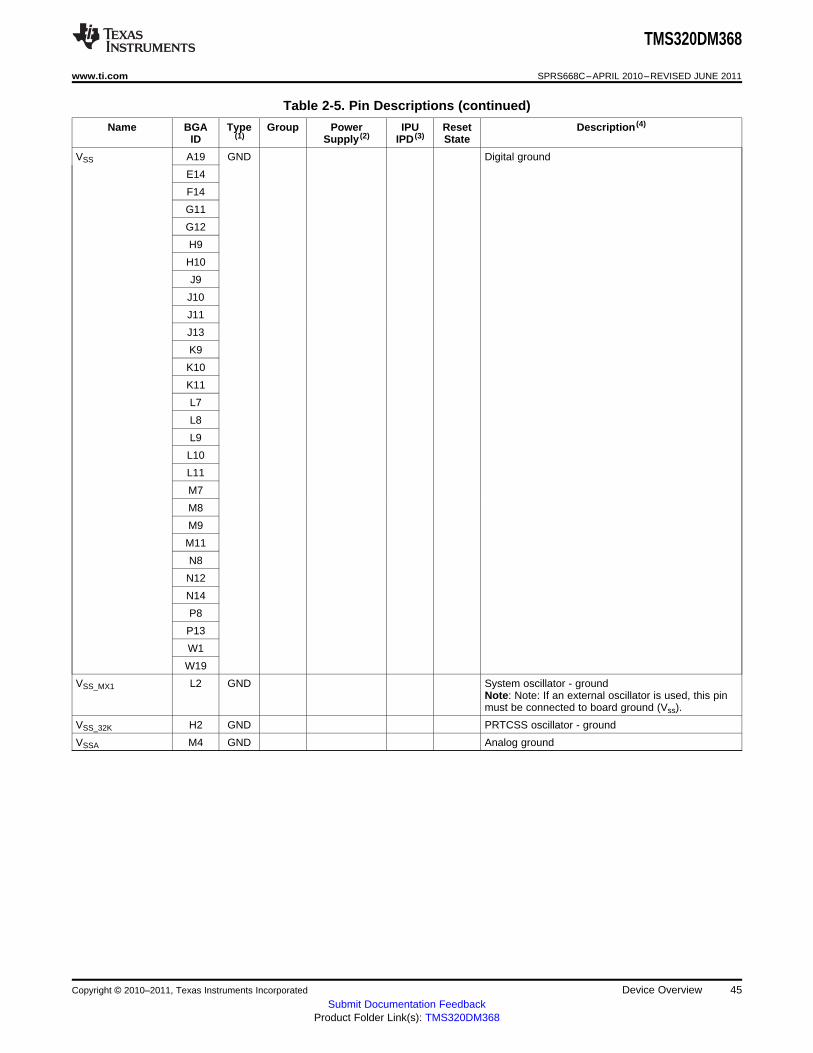
TMS320DM368
www.ti.com SPRS668C–APRIL 2010–REVISED JUNE 2011
Table 2-5. Pin Descriptions (continued)
Name BGA Type Group Power IPU Reset Description (4)
ID (1) Supply (2) IPD (3) State
VSS A19 GND Digital ground
E14
F14
G11
G12
H9
H10
J9
J10
J11
J13
K9
K10
K11
L7
L8
L9
L10
L11
M7
M8
M9
M11
N8
N12
N14
P8
P13
W1
W19
VSS_MX1 L2 GND System oscillator - groundNote: Note: If an external oscillator is used, this pinmust be connected to board ground (Vss).
VSS_32K H2 GND PRTCSS oscillator - ground
VSSA M4 GND Analog ground
Copyright © 2010–2011, Texas Instruments Incorporated Device Overview 45Submit Documentation Feedback
Product Folder Link(s): TMS320DM368

TMS320DM368
SPRS668C–APRIL 2010–REVISED JUNE 2011 www.ti.com
2.9 Device Support
2.9.1 Development Tools
TI offers an extensive line of development tools for device systems, including tools to evaluate theperformance of the processors, generate code, develop algorithm implementations, and fully integrate anddebug software and hardware modules. The tools support documentation is electronically available withinthe Code Composer Studio™ Integrated Development Environment (IDE).
The following products support development of device based applications:
Software Development Tools:Code Composer Studio™ Integrated Development Environment (IDE): including Editor
C/C++/Assembly Code Generation, and Debug plus additional development toolsHardware Development Tools:
Extended Development System (XDS™) Emulator (supports TMS320DM368 DMSoC multiprocessorsystem debug) EVM (Evaluation Module)For a complete listing of development-support tools for the TMS320DM368 DMSoC platform, visit theTexas Instruments web site on the Worldwide Web at www.ti.com. For information on pricing andavailability, contact the nearest TI field sales office or authorized distributor.
2.9.2 Device Nomenclature
To designate the stages in the product development cycle, TI assigns prefixes to the part numbers of allDSP devices and support tools. Each DSP commercial family member has one of three prefixes: TMX,TMP, or TMS (e.g., ). Texas Instruments recommends two of three possible prefix designators for itssupport tools: TMDX and TMDS. These prefixes represent evolutionary stages of product developmentfrom engineering prototypes (TMX/TMDX) through fully qualified production devices/tools (TMS/TMDS).
Device development evolutionary flow:
TMX Experimental device that is not necessarily representative of the final device's electricalspecifications.
TMP Final silicon die that conforms to the device's electrical specifications but has not completedquality and reliability verification.
TMS Fully-qualified production device.
Support tool development evolutionary flow:
TMDX Development-support product that has not yet completed Texas Instruments internalqualification testing.
TMDS Fully qualified development-support product.
TMX and TMP devices and TMDX development-support tools are shipped against the followingdisclaimer:
"Developmental product is intended for internal evaluation purposes."
TMS devices and TMDS development-support tools have been characterized fully, and the quality andreliability of the device have been demonstrated fully. TI's standard warranty applies.
Predictions show that prototype devices (TMX or TMP) have a greater failure rate than the standardproduction devices. Texas Instruments recommends that these devices not be used in any productionsystem because their expected end-use failure rate is undefined. Only qualified production devices are tobe used in production.
46 Device Overview Copyright © 2010–2011, Texas Instruments Incorporated
Submit Documentation FeedbackProduct Folder Link(s): TMS320DM368

PREFIXTMX = Experimental deviceTMS = Production device
TMS 320 DM368 ZCE ( )
DEVICE FAMILY320 = TMS320 DSP family
PACKAGE TYPEZCE = 338-pin plastic BGA with Pb-free soldered balls
(A)
DEVICEDM368
(B)
ABC
. BGA = Ball Grid Array
. For actual device part numbers (P/Ns) and ordering information, contact your nearest TI Sales Representative.
. For more information on silicon revision, see the (literature number SPRZ316).TMS320DM368 Silicon Errata
( )
SILICON REVISION(C)
( )
TEMPERATURE GRADEBlank = 0 to 85CD = -40 to 85C
F = Face Detection
TMS320DM368
www.ti.com SPRS668C–APRIL 2010–REVISED JUNE 2011
TI device nomenclature also includes a suffix with the device family name. This suffix indicates thepackage type (for example, ZCE), the temperature range (for example, "Blank" is the commercialtemperature range), and the device speed range in megahertz (for example, 202 is 202.5 MHz). Thefollowing figure provides a legend for reading the complete device name for any TMS320DM368 DMSoCplatform member.
Figure 2-6. Device Nomenclature
2.9.3 Related Documentation From Texas Instruments
The following documents describe the TMS320DM36x Digital Media System-on-Chip (DMSoC). Copies ofthese documents are available on the internet at www.ti.com.
SPRZ315 TMS320DM368 DMSoC Silicon Errata Describes the known exceptions to the functionalspecifications for the TMS320DM368 DMSoC.
SPRUFG5 TMS320DM36x Digital Media System-on-Chip (DMSoC) ARM Subsystem Users Guide.This document describes the ARM Subsystem in the TMS320DM36x Digital MediaSystem-on-Chip (DMSoC). The ARM subsystem is designed to give the ARM926EJ-S(ARM9) master control of the device. In general, the ARM is responsible for configurationand control of the device; including the components of the ARM Subsystem, the peripherals,and the external memories.
SPRUFG8 TMS320DM36x Digital Media System-on-Chip (DMSoC) Video Processing Front End(VPFE) Users Guide. This document describes the Video Processing Front End (VPFE) inthe TMS320DM36x Digital Media System-on-Chip (DMSoC).
SPRUFG9 TMS320DM36x Digital Media System-on-Chip (DMSoC) Video Processing Back End(VPBE) Users Guide. This document describes the Video Processing Back End (VPBE) inthe TMS320DM36x Digital Media System-on-Chip (DMSoC).
SPRUFH0 TMS320DM36x Digital Media System-on-Chip (DMSoC) 64-bit Timer Users Guide. Thisdocument describes the operation of the software-programmable 64-bit timers in theTMS320DM36x Digital Media System-on-Chip (DMSoC).
SPRUFH1 TMS320DM36x Digital Media System-on-Chip (DMSoC) Serial Peripheral Interface (SPI)Users Guide. This document describes the serial peripheral interface (SPI) in theTMS320DM36x Digital Media System-on-Chip (DMSoC). The SPI is a high-speedsynchronous serial input/output port that allows a serial bit stream of programmed length (1to 16 bits) to be shifted into and out of the device at a programmed bit-transfer rate. The SPIis normally used for communication between the DMSoC and external peripherals. Typicalapplications include an interface to external I/O or peripheral expansion via devices such as
Copyright © 2010–2011, Texas Instruments Incorporated Device Overview 47Submit Documentation Feedback
Product Folder Link(s): TMS320DM368

TMS320DM368
SPRS668C–APRIL 2010–REVISED JUNE 2011 www.ti.com
shift registers, display drivers, SPI EPROMs and analog-to-digital converters.
SPRUFH2 TMS320DM36x Digital Media System-on-Chip (DMSoC) Universal AsynchronousReceiver/Transmitter (UART) Users Guide. This document describes the universalasynchronous receiver/transmitter (UART) peripheral in the TMS320DM36x Digital MediaSystem-on-Chip (DMSoC). The UART peripheral performs serial-to-parallel conversion ondata received from a peripheral device, and parallel-to-serial conversion on data receivedfrom the CPU.
SPRUFH3 TMS320DM36x Digital Media System-on-Chip (DMSoC) Inter-Integrated Circuit (I2C)Peripheral Users Guide. This document describes the inter-integrated circuit (I2C)peripheral in the TMS320DM36x Digital Media System-on-Chip (DMSoC). The I2C peripheralprovides an interface between the DMSoC and other devices compliant with the I2C-busspecification and connected by way of an I2C-bus.
SPRUFH5 TMS320DM36x Digital Media System-on-Chip (DMSoC) Multimedia Card (MMC)/SecureDigital (SD) Card Controller Users Guide. This document describes the multimedia card(MMC)/secure digital (SD) card controller in the TMS320DM36x Digital MediaSystem-on-Chip (DMSoC).
SPRUFH6 TMS320DM36x Digital Media System-on-Chip (DMSoC) Pulse-Width Modulator (PWM)Users Guide. This document describes the pulse-width modulator (PWM) peripheral in theTMS320DM36x Digital Media System-on-Chip (DMSoC).
SPRUFH7 TMS320DM36x Digital Media System-on-Chip (DMSoC) Real-Time Out (RTO) ControllerUsers Guide. This document describes the Real Time Out (RTO) controller in theTMS320DM36x Digital Media System-on-Chip (DMSoC).
SPRUFH8 TMS320DM36x Digital Media System-on-Chip (DMSoC) General-Purpose Input/Output(GPIO) Users Guide. This document describes the general-purpose input/output (GPIO)peripheral in the TMS320DM36x Digital Media System-on-Chip (DMSoC). The GPIOperipheral provides dedicated general-purpose pins that can be configured as either inputsor outputs.
SPRUFH9 TMS320DM36x Digital Media System-on-Chip (DMSoC) Universal Serial Bus (USB)Controller Users Guide. This document describes the universal serial bus (USB) controllerin the TMS320DM36x Digital Media System-on-Chip (DMSoC). The USB controller supportsdata throughput rates up to 480 Mbps. It provides a mechanism for data transfer betweenUSB devices and also supports host negotiation.
SPRUFI0 TMS320DM36x Digital Media System-on-Chip (DMSoC) Enhanced Direct MemoryAccess (EDMA) Controller Users Guide. This document describes the operation of theenhanced direct memory access (EDMA3) controller in the TMS320DM36x Digital MediaSystem-on-Chip (DMSoC). The EDMA controller's primary purpose is to serviceuser-programmed data transfers between two memory-mapped slave endpoints on theDMSoC.
SPRUFI1 TMS320DM36x Digital Media System-on-Chip (DMSoC) Asynchronous ExternalMemory Interface (EMIF) Users Guide. This document describes the asynchronousexternal memory interface (EMIF) in the TMS320DM36x Digital Media System-on-Chip(DMSoC). The EMIF supports a glueless interface to a variety of external devices.
SPRUFI2 TMS320DM36x Digital Media System-on-Chip (DMSoC) DDR2/Mobile DDR(DDR2/mDDR) Memory Controller Users Guide. This document describes theDDR2/mDDR memory controller in the TMS320DM36x Digital Media System-on-Chip(DMSoC). The DDR2/mDDR memory controller is used to interface with JESD79D-2Astandard compliant DDR2 SDRAM and mobile DDR devices.
SPRUFI3 TMS320DM36x Digital Media System-on-Chip (DMSoC) Multibuffered Serial PortInterface (McBSP) User's Guide. This document describes the operation of the
48 Device Overview Copyright © 2010–2011, Texas Instruments Incorporated
Submit Documentation FeedbackProduct Folder Link(s): TMS320DM368

TMS320DM368
www.ti.com SPRS668C–APRIL 2010–REVISED JUNE 2011
multibuffered serial host port interface in the TMS320DM36x Digital Media System-on-Chip(DMSoC). The primary audio modes that are supported by the McBSP are the AC97 and IISmodes. In addition to the primary audio modes, the McBSP supports general serial portreceive and transmit operation.
SPRUFI4 TMS320DM36x Digital Media System-on-Chip (DMSoC) Universal Host Port Interface(UHPI) User's Guide. This document describes the operation of the universal host portinterface in the TMS320DM36x Digital Media System-on-Chip (DMSoC).
SPRUFI5 TMS320DM36x Digital Media System-on-Chip (DMSoC) Ethernet Media AccessController (EMAC) User's Guide. This document describes the operation of the ethernetmedia access controllerface in the TMS320DM36x Digital Media System-on-Chip (DMSoC).
SPRUFI7 TMS320DM36x Digital Media System-on-Chip (DMSoC) Analog to Digital Converter(ADC) User's Guide. This document describes the operation of the analog to digitalconversion in the TMS320DM36x Digital Media System-on-Chip (DMSoC).
SPRUFI8 TMS320DM36x Digital Media System-on-Chip (DMSoC) Key Scan User's Guide. Thisdocument describes the key scan peripheral in the TMS320DM36x Digital MediaSystem-on-Chip (DMSoC).
SPRUFI9 TMS320DM36x Digital Media System-on-Chip (DMSoC) Voice Codec User's Guide. Thisdocument describes the voice codec peripheral in the TMS320DM36x Digital MediaSystem-on-Chip (DMSoC). This module can access ADC/DAC data with internal FIFO (ReadFIFO/Write FIFO). The CPU communicates to the voice codec module using 32-bit-widecontrol registers accessible via the internal peripheral bus.
SPRUFJ0 TMS320DM36x Digital Media System-on-Chip (DMSoC) Power Management andReal-Time Clock Subsystem (PRTCSS) User's Guide. This document provides afunctional description of the Power Management and Real-Time Clock Subsystem(PRTCSS) in the TMS320DM36x Digital Media System-on-Chip (DMSoC) and PRTCinterface (PRTCIF).
Copyright © 2010–2011, Texas Instruments Incorporated Device Overview 49Submit Documentation Feedback
Product Folder Link(s): TMS320DM368

TMS320DM368
SPRS668C–APRIL 2010–REVISED JUNE 2011 www.ti.com
3 Device Configurations
This section provides a detailed overview of the device.
3.1 System Module Registers
The system module includes status and control registers for configuration of the device. Brief descriptionsof the various registers are shown in Table 3-1. For more information on the System Module registers, seethe TMS320DM36x DMSoC ARM Subsystem Reference Guide (literature number SPRUFG5).
Table 3-1. System Module Register Memory Map
HEX ADDRESS REGISTER ACRONYM DESCRIPTION (1)
0x01C4 0000 PINMUX0 Pin Mux 0 (Video In) Pin Mux Register
0x01C4 0004 PINMUX1 Pin Mux 1 (Video Out) Pin Mux Register
0x01C4 0008 PINMUX2 Pin Mux 2 (AEMIF) Pin Mux Register
0x01C4 000C PINMUX3 Pin Mux 3 (GIO/Misc) Pin Mux Register
0x01C4 0010 PINMUX4 Pin Mux 4 (Misc) Pin Mux Register
0x01C4 0014 BOOTCFG Boot Configuration
0x01C4 0018 ARM_INTMUX Multiplexing Control for Interrupts
0x01C4 001C EDMA_EVTMUX Multiplexing Control for EDMA Events
0x01C4 0020 DDR_SLEW DDR Slew Rate
0x01C4 0024 UHPICTL UHPI Control
0x01C4 0028 DEVICE_ID Device ID
0x01C4 002C VDAC_CONFIG Video DAC Configuration
0x01C4 0030 TIMER64_CTL Timer64 Input Control
0x01C4 0034 USB_PHY_CTL USB PHY Control
0x01C4 0038 MISC Miscellaneous Control
0x01C4 003C MSTPRI0 Master Priorities Register 0
0x01C4 0040 MSTPRI1 Master Priorities Register 1
0x01C4 0044 VPSS_CLK_CTL VPSS Clock Mux Control
0x01C4 0048 PERI_CLKCTL Peripheral Clock Control
0x01C4 004C DEEPSLEEP DEEPSLEEP Control
0x01C4 0050 - Reserved
0x01C4 0054 DEBOUNCE0 Debounce for GIO0 Input
0x01C4 0058 DEBOUNCE1 Debounce for GIO1 Input
0x01C4 005C DEBOUNCE2 Debounce for GIO2 Input
0x01C4 0060 DEBOUNCE3 Debounce for GIO3 Input
0x01C4 0064 DEBOUNCE4 Debounce for GIO4 Input
0x01C4 0068 DEBOUNCE5 Debounce for GIO5 Input
0x01C4 006C DEBOUNCE6 Debounce for GIO6 Input
0x01C4 0070 DEBOUNCE7 Debounce for GIO7 Input
0x01C4 0074 VTPIOCR VTP IO Control
0x01C4 0078 PUPDCTL0 IO cell pullup/down on/off control #0
0x01C4 007C PUPDCTL1 IO cell pullup/down on/off control #1
0x01C4 0080 HDVICPBT HDVICP Boot Register
0x01C4 0084 PLL1_CONFIG PLL1 Configuration Register
0x01C4 0088 PLL2_CONFIG PLL2 Configuration Register
(1) For more details on the system module registers, see the TMS320DM36x DMSoC ARM Subsystem Reference Guide (literature numberSPRUFG5).
50 Device Configurations Copyright © 2010–2011, Texas Instruments Incorporated
Submit Documentation FeedbackProduct Folder Link(s): TMS320DM368

TMS320DM368
www.ti.com SPRS668C–APRIL 2010–REVISED JUNE 2011
3.2 Boot Modes
The ARM can boot from either Asynchronous EMIF (OneNand/NOR) or from ARM ROM, as determinedby the setting of the device configuration pins BTSEL[2:0]. The boot selection pins (BTSEL[2:0]) determinethe ARM boot process. After reset (POR, warm reset, or max reset), ARM program execution begins inARM ROM at 0x0000: 8000, except when BTSEL[2:0] = 001, indicating AEMIF (OneNand/NOR) flashboot.
3.2.1 Boot Modes Overview
The ARM ROM boot loader (RBL) executes when the BTSEL[2:0] pins indicate a condition other than thenormal ARM EMIF boot.• If BTSEL[2:0] = 001 - Asynchronous EMIF boot mode (NOR or OneNAND). This mode is handled by
hardware control and does not involve the ROM. In the case of OneNAND, the user is responsible forputting any necessary boot code in the OneNAND's boot page. This code shall configure the AEMIFmodule for the OneNAND device. After the AEMIF module is configured, booting will continueimmediately after the OneNAND’s boot page with the AEMIF module managing pages thereafter.
• The RBL supports 7 distinct boot modes:– BTSEL[2:0] = 000 - NAND Boot mode– BTSEL[2:0] = 010 - MMC0/SD0 Boot mode– BTSEL[2:0] = 011 - UART0 Boot mode– BTSEL[2:0] = 100 - USB Boot mode– BTSEL[2:0] = 101 - SPI0 Boot mode– BTSEL[2:0] = 110 - EMAC Boot mode– BTSEL[2:0] = 111 - HPI Boot mode
• If NAND boot fails, then MMC/SD mode is tried.• If MMC/SD boot fails, then MMC/SD boot is tried again.• If UART boot fails, then UART boot is tried again.• If USB boot fails, then USB boot is tried again.• If SPI boot fails, then SPI boot is tried again.• If EMAC boot fails, then EMAC boot is tried again.• If HPI boot fails, then HPI boot is tried again.• RBL shall update boot status (PASS/FAIL) in MISC register bits 8 and 9 in System control module.• ARM ROM Boot - NAND Mode
– No support for a full firmware boot. Instead, copies a second stage user boot loader (UBL) fromNAND flash to ARM internal RAM (AIM) and transfers control to the user-defined UBL.
– Support for NAND with page sizes up to 4096 bytes.– Support for magic number error detection and retry (up to 24 times) when loading UBL– Support for up to 30KB UBL (32KB IRAM - ~2KB for RBL stack)– Optional, user-selectable, support for use of DMA and I-cache during RBL execution (i.e.,while
loading UBL)– Supports booting from 8-bit NAND devices (16-bit NAND devices are not supported)– Uses/Requires 4-bit HW ECC (NAND devices with ECC requirements ≤ 4 bits per 512 bytes are
supported)– Supports NAND flash that requires chip select to stay low during the tR read time
Copyright © 2010–2011, Texas Instruments Incorporated Device Configurations 51Submit Documentation Feedback
Product Folder Link(s): TMS320DM368
TMS320DM368
SPRS668C–APRIL 2010–REVISED JUNE 2011 www.ti.com
• ARM ROM Boot - MMC/SD Mode– No support for a full firmware boot. Instead, copies a second stage User Boot Loader (UBL) from
MMC/SD to ARM Internal RAM (AIM) and transfers control to the user software.– Support for MMC/SD Native protocol (MMC/SD SPI protocol is not supported)– Support for descriptor error detection and retry (up to 24 times) when loading UBL– Support for up to 30KB UBL (32KB - ~2KB for RBL stack)– SDHC boot supported by RBL
• ARM ROM Boot - UART mode– If the state of BTSEL[2:0] pins at reset is 011, then the UART boot mode executes. This mode
enables a small program, referred to here as a user boot loader (UBL), to be downloaded to theon-chip ARM internal RAM via the on-chip serial UART and executed. A host program, (referred toas serial host utility program), manages the interaction with RBL and provides a means for operatorfeedback and input. The UART boot mode execution assumes the following UART settings: 24MHz reference clock, Time-Out 500 ms, one-shot Serial RS-232 port 115.2 Kbps, 8-bit, no parity,one stop bit Command, data, and checksum format Everything sent from the host to the deviceUART RBL must be in ASCII format
– No support for a full firmware boot. Instead, loads a second stage user boot loader (UBL) via UARTto ARM internal RAM (AIM) and transfers control to the user software.
– Support for up to 30KB UBL (32KB - ~2KB for RBL stack)• ARM ROM Boot – USB Mode
– No support for a full firmware boot. Instead, loads a second stage User Boot Loader (UBL) via USBto ARM Internal RAM (AIM) and transfers control to the users software.
• ARM ROM Boot – SPI Mode– The device will copy UBL to ARM Internal RAM (AIM) via SPI interface from a SPI peripheral like
SPI EEPROM. RBL will then transfer control to the UBL.• ARM ROM Boot – EMAC Mode
– The device will send a boot request packet and the host/server will respond with the boot packets.RBL will wait for all boot packets to arrive and then transfer control to the UBL which is received viaboot packets. In EMAC boot mode an I2C EEPROM or SPI EEPROM is necessary forprogramming EMAC descriptor (including EMAC address for the device)Note: If a magic number is not found in the EEPROM, then the EMAC boot mode will use a defaultMAC address. In this case, there will be no magic number support.
• ARM ROM Boot – HPI Mode– The Host will copy UBL to ARM Internal RAM (AIM) via HPI interface and notify the ROM
bootloader after copy is finished. RBL will then transfer control to the UBL.
The general boot sequence is shown in Figure 3-1. For more information, refer to the TMS320DM36xDMSoC ARM Subsystem Reference Guide (literature number SPRUFG5).
52 Device Configurations Copyright © 2010–2011, Texas Instruments Incorporated
Submit Documentation FeedbackProduct Folder Link(s): TMS320DM368

NAND
Boot
Boot
OK
?
No
Yes
MMCSD
Boot
Boot
OK
?
No
Yes
NAND
UART
Boot
Boot
OK
?
No
Yes
UARTMMCSD
USB
Boot
Boot
OK
?
No
Yes
USB
SPI
Boot
Boot
OK
?
No
Yes
SPI
EMAC
Boot
Boot
OK
?
No
Yes
EMAC
HPI
Boot
Boot
OK
?
No
Yes
HPI
RBL
Boot
?
Reset
One NAND/NOR Boot
AEMIF
UBL
ROM Boot Loader
No
Yes
TMS320DM368
www.ti.com SPRS668C–APRIL 2010–REVISED JUNE 2011
Figure 3-1. Boot Mode Functional Block Diagram
Copyright © 2010–2011, Texas Instruments Incorporated Device Configurations 53Submit Documentation Feedback
Product Folder Link(s): TMS320DM368

TMS320DM368
SPRS668C–APRIL 2010–REVISED JUNE 2011 www.ti.com
3.3 Device Clocking
3.3.1 Overview
The device requires one primary reference clock. The reference clock frequency may be generated eitherby crystal input or by external oscillator. The reference clock is the clock at the pins named MXI1/MXO1,and which drives two separate PLL controllers (PLLC1 and PLLC2). PLLC1 generates the clocks requiredby the ARM, EDMA, VPSS and the rest of the peripherals. PLL2 generates the clock required by the DDRPHY interface and is also capable of providing clocks to the ARM, USB, Video, or Voice Codec modulesas well as a flexible clocking option. Figure 3-2 represents the clocking architecture for the ARMsubsystem. For more information on device clocking and the system PLL controller please see theTMS320DM36x DMSoC ARM Subsystem Reference Guide (literature number SPRUFG5).
54 Device Configurations Copyright © 2010–2011, Texas Instruments Incorporated
Submit Documentation FeedbackProduct Folder Link(s): TMS320DM368

Oscillator (MXI1/MXO1)19.2/24/27/36 Mhz
SPI4
I2C
UART0
TIMER0-3/WDT
PWM0-3
ADC
RTO
MMC/SD0
McBSP
MMC/SD1
UART1
AEMIF
SPI0-3
GPIO
AINTC
EMAC
EDMA
HPI
USB PHY
USB
CLKOUT0
CLKOUT1
DIV1CLKOUT2
DDRPHY
DDR2EMIF
EXTCLK
PCLK
VPBE
VPFE
ARMSSHDVICP
MJCP
VPSS
VoiceCodec
DIV2
DIV3
KeyScan PRTCSS
32 KhzOscillator
PLLC1 PLLC2
VPSS_MUXSELVENC_CLK_SRC
PHYCLKSRC
PRTCCLKS
KEYSCLKS
DDRCLKS
VCLK
MC
LK
SY
SC
LK
1
SY
SC
LK
2
SY
SC
LK
3
SY
SC
LK
4
SY
SC
LK
5
OB
SC
LK
SY
SC
LK
3
SY
SC
LK
2
SY
SC
LK
1
SY
SC
LK
6
SY
SC
LK
5
SY
SC
LK
4
SY
SC
LK
7
OB
SC
LK
SY
SC
LK
9
SY
SC
LK
8
SY
SC
LK
BP
TMS320DM368
www.ti.com SPRS668C–APRIL 2010–REVISED JUNE 2011
Figure 3-2. Clocking Architecture
3.3.2 PLL Controller Module
Two PLL controllers provide clocks to different components of the chip. The PLL controller 1 (PLLC1)provides clocks to most of the components of the chip. The PLL controller 2 (PLLC2) provides clocks tothe DDR PHY and is also capable of providing clocks to the ARM, USB, VPSS or the Voice Codecmodules instead as well.
As a module, the PLL controller provides the following:• Glitch-free transitions (on changing PLL settings)• Domain clocks alignment• Clock gating
Copyright © 2010–2011, Texas Instruments Incorporated Device Configurations 55Submit Documentation Feedback
Product Folder Link(s): TMS320DM368
TMS320DM368
SPRS668C–APRIL 2010–REVISED JUNE 2011 www.ti.com
• PLL bypass• PLL power down
The various clock outputs given by the PLL controller are as follows:• Domain clocks: SYSCLKn• Bypass domain clock: SYSCLKBP• Auxiliary clock from reference clock: AUXCLK
Various dividers that can be used are as follows:• Pre-PLL divider: PREDIV• Post-PLL divider: POSTDIV• SYSCLK divider: PLLDIV1, …, PLLDIVn• SYSCLKBP divider: BPDIV
The Multiplier values supported are handled by:• PLL multiplier control: PLLM
Notes:• PLLCxSYSCLKy is used to denote post divide clock output SYSCLKy from PLL controller x• 'x', which denotes PLL Controller number, can assume values 1 and 2• 'y', which denotes post divide clock outputs, can assume values 1 to 9 in case of PLLC1 and 1 to 5 in
case of PLLC2
The PLL Controllers for PLL1 and PLL2 are described in detail in the TMS320DM36x ARM SubsystemReference Guide (literature number SPRUFG5).
56 Device Configurations Copyright © 2010–2011, Texas Instruments Incorporated
Submit Documentation FeedbackProduct Folder Link(s): TMS320DM368

TMS320DM368
www.ti.com SPRS668C–APRIL 2010–REVISED JUNE 2011
3.3.3 PLLC1
There are two PLLs on the device, and they are independently controlled. PLLC1 generates thefrequencies needed for the ARM, Video Processing Sub System (VPSS), MJCP coprocessor block,EDMA, and peripherals.
The reference clock for both PLLs is the single crystal input. Both PLLs will be of the same type . It shouldbe noted that the USB2.0 PHY contains a third PLL embedded within it. Table 3-2, and Figure 3-3describe the customization of PLLC1.• Provides primary system clock• Software configurable• Accepts clock input or internal oscillator input• PLL pre-divider value is programmable• PLL multiplier value is programmable• PLL post-divider value is programmable . See the data manual for all supported configurations.• Only SYSCLK [9:1] are used
Table 3-2. PLLC1 Output Clocks
PLLC1SYSCLKy Used By PLLDIV Divider
PLLC1SYSCLK1 USB reference clock (1) Programmable
PLLC1SYSCLK2 ARM926EJ-S, HDVICP block clock (1) Programmable
PLLC1SYSCLK3 MJCP and HDVICP bus interface clock Programmable
PLLC1SYSCLK4 Configuration bus clock, peripheral system interfaces, ProgrammableEDMA
PLLC1SYSCLK5 VPSS clock Programmable
PLLC1SYSCLK6 VENC clock (1) Programmable
PLLC1SYSCLK7 DDR 2x clock (1) Programmable
PLLC1SYSCLK8 MMC/SD0 clock Programmable
PLLC1SYSCLK9 CLKOUT2 Programmable
PLLC1OBSCLK CLKOUT0 Programmable
PLLC1SYSCLKBP USB reference clock (1) Programmable
(1) These clock outputs are multiplexed with other clocks.
Copyright © 2010–2011, Texas Instruments Incorporated Device Configurations 57Submit Documentation Feedback
Product Folder Link(s): TMS320DM368

Pre-DIV(Programmable)
PLL 1
0
PLLEN
PLLM(Programmable)
Post-DIV(Programmable)
OSCIN
PLLDIV1* SYSCLK1 (USB Reference Clock)
PLLDIV2* SYSCLK2 (ARM926EJ-S, HDVICPBlock Clock)
PLLDIV3* SYSCLK3 (MJCP and HDVICPCoprocessors Bus Interface Clock)
PLLDIV4* SYSCLK4 (Config Bus, Peripheral SystemInterfaces, EDMA)
PLLDIV5* SYSCLK5 (VPSS)
PLLDIV6* SYSCLK6 (VENC Clock)
PLLDIV7* SYSCLK7 (DDR 2x Clock)
PLLDIV8* SYSCLK8 (MMC/SD0 Clock)
PLLDIV9* SYSCLK9 (CLKOUT 2)
OSCDIV1*
BPDIV*
OBSCLK (CLKOUT0)
SYSCLKBP (
* – Programmable
USB Reference Clock)
TMS320DM368
SPRS668C–APRIL 2010–REVISED JUNE 2011 www.ti.com
Figure 3-3. PLLC1 Configuration
3.3.4 PLLC2
PLLC2 provides the USB reference clock, ARM926EJ-S, DDR 2x clock, Voice Codec clock and VENC27MHz, 74.25MHz clock. The PLLC2 functionality can be programmed via the PLLC2 registers. Thefollowing list, Table 3-3, and Figure 3-4 describe the customization of PLLC2.
The PLLC2 customization includes the following features:• PLLC2 provides DDR PHY, USB reference clock , ARM926EJ-S clock, VENC 27MHz, 74.25Hz clock
and Voice codec clock• Software configurable• Accepts clock input or internal oscillator input (the same input as PLLC1)• PLL pre-divider value is programmable• PLL multiplier value is programmable• PLL post-divider value is programmable• Only SYSCLK [5:1] are used
Table 3-3. PLLC2 Output Clocks
PLLC2SYSCLKy Used by PLLDIV Divider
PLLC2SYSCLK1 USB reference clock (1) Programmable
PLLC2SYSCLK2 ARM926EJ-S, HDVICP block clock (1) Programmable
PLLC2SYSCLK3 DDR 2x clock (1) Programmable
PLLC2SYSCLK4 Voice Codec clock Programmable
PLLC2SYSCLK5 VENC clock (1) Programmable
PLLC2OBSCLK CLKOUT1 Programmable
(1) These clock outputs are multiplexed with other clocks.
58 Device Configurations Copyright © 2010–2011, Texas Instruments Incorporated
Submit Documentation FeedbackProduct Folder Link(s): TMS320DM368
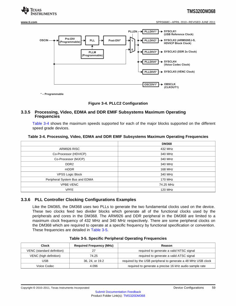
Pre-DIV(Programmable)
PLL 1
0
PLLEN
PLLM(Programmable)
Post-DIV*OSCIN
PLLDIV1* SYSCLK1(USB Reference Clock)
PLLDIV2* SYSCLK2 (ARM926EJ-S,HDVICP Block Clock)
PLLDIV3* SYSCLK3 (DDR 2x Clock)
PLLDIV4* SYSCLK4(Voice Codec Clock)
PLLDIV5* SYSCLK5 (VENC Clock)
OSCDIV1* OBSCLK(CLKOUT1)
* – Programmable
TMS320DM368
www.ti.com SPRS668C–APRIL 2010–REVISED JUNE 2011
Figure 3-4. PLLC2 Configuration
3.3.5 Processing, Video, EDMA and DDR EMIF Subsystems Maximum OperatingFrequencies
Table 3-4 shows the maximum speeds supported for each of the major blocks supported on the differentspeed grade devices.
Table 3-4. Processing, Video, EDMA and DDR EMIF Subsystems Maximum Operating Frequencies
DM368
ARM926 RISC 432 MHz
Co-Processor (HDVICP) 340 MHz
Co-Processor (MJCP) 340 MHz
DDR2 340 MHz
mDDR 168 MHz
VPSS Logic Block 340 MHz
Peripheral System Bus and EDMA 170 MHz
VPBE-VENC 74.25 MHz
VPFE 120 MHz
3.3.6 PLL Controller Clocking Configurations Examples
Like the DM365, the DM368 uses two PLLs to generate the two fundamental clocks used on the device.These two clocks feed two divider blocks which generate all of the functional clocks used by theperipherals and cores in the DM368. The ARM926 and DDR peripheral in the DM368 are limited to amaximum clock frequency of 432 MHz and 340 MHz respectively. There are some peripheral clocks onthe DM368 which are required to operate at a specific frequency by functional specification or convention.These frequencies are detailed in Table 3-5.
Table 3-5. Specific Peripheral Operating Frequencies
Clock Required Frequency (MHz) Reason
VENC (standard definition) 27 required to generate a valid NTSC signal
VENC (high definition) 74.25 required to generate a valid ATSC signal
USB 36, 24, or 19.2 required by the USB peripheral to generate a 48 MHz USB clock
Voice Codec 4.096 required to generate a precise 16 kHz audio sample rate
Copyright © 2010–2011, Texas Instruments Incorporated Device Configurations 59Submit Documentation Feedback
Product Folder Link(s): TMS320DM368
TMS320DM368
SPRS668C–APRIL 2010–REVISED JUNE 2011 www.ti.com
While it is possible to generate both a 432 MHz and 340 MHz clock with the two PLLs, these twofrequencies cannot be divided down to generate all required frequencies from Table 3-5. Several differentfrequency solutions are required to cover all of these requirements. The different solutions for differentinput crystal frequencies are listed in the tables below.
The following tables show examples of the PLL combinations that can be supported with DM368. Pleasesee the TMS320DM36x DMSoC ARM Subsystem Reference Guide (literature number SPRUFG5) foradditional details on special peripherals clocking considerations and for additional PLL controllerconfiguration details.
There are several important points to note from these tables.• A 432 MHz functional clock will result in DM368 voice codec sampling frequency of 16.07KHz. The
difference of 0.4375% versus 16KHz specification should be acceptable for the majority of audioapplications. If the DM368 voice codec is required to operate at precisely 16 kHz then the functionalclock can be reduced to achieve precisely that sample frequency but the ARM926 and HDVICP willhave to run at a reduced rate resulting in lower video performance.
• If a 24 MHz input crystal is used it is not possible to generate a 74.25 MHz HD video output clock.• If a 19.2 MHz input crystal is used it is not possible to generate a valid 74.25 MHz HD output clock.
Table 3-6. 24-MHz Input Crystal Example (1) (2) (3)
PLL1 PLL2 ARM DDR MJCP HDVICP Voice Codec (4) Video Encoder
PLL Output (2M/(N+1)) PLL Output (2M/(N+1)) 27MHz 74.25MHz(5)(MHz) (MHz)
680 170/6 432 18/1 432 340 340 340 1/105 (16.06 1/16 -kHz)
680 170/6 430.08 448/25 430.08 340 340 340 1/105 - -
(1) M = PLL controller multiplier. N = PLL controller divider.(2) All shaded frequencies derive from the PLL2 controller.(3) PLLC1SYSCLK4 (Configuration bus clock, peripheral system interfaces, EDMA) should be half of the PLLC1SYSCLK3 (MJCP and
HDVICP bus interface clock).(4) The Voice Codec divider value is the combination of the PLL controller 2 SYSCLK4 and Peripheral Clock Control Register PLLDIV2 bit
setting divider.(5) PLL Output is calculated by = Oscillator Input * (2M/(N+1)).
Table 3-7. 36-MHz Input Crystal Example (1) (2) (3)
PLL1 PLL2 ARM DDR MJCP HDVICP Voice Codec (4) Video Encoder
PLL Output(5) (2M/(N+1)) PLL Output (2M/(N+1)) 27MHz 74.25MHz(MHz) (MHz)
680 510/27 432 12/1 432 340 340 340 1/105 (16.07 1/16 -kHz)
680 680/27 371.25 330/32 371.25 340 340 340 1/91 (15.936 - 1/5kHz)
(1) M = PLL controller multiplier. N = PLL controller divider.(2) All shaded frequencies derive from the PLL2 controller.(3) PLLC1SYSCLK4 (Configuration bus clock, peripheral system interfaces, EDMA) should be half of the PLLC1SYSCLK3 (MJCP and
HDVICP bus interface clock).(4) The Voice Codec divider value is the combination of the PLL controller 2 SYSCLK4 and Peripheral Clock Control Register PLLDIV2 bit
setting divider.(5) PLL Output is calculated by = Oscillator Input * (2M/(N+1)).
60 Device Configurations Copyright © 2010–2011, Texas Instruments Incorporated
Submit Documentation FeedbackProduct Folder Link(s): TMS320DM368
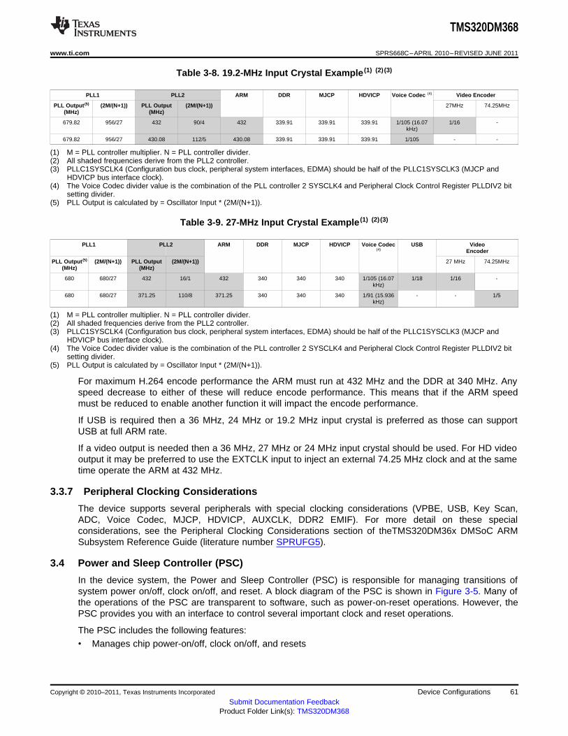
TMS320DM368
www.ti.com SPRS668C–APRIL 2010–REVISED JUNE 2011
Table 3-8. 19.2-MHz Input Crystal Example (1) (2) (3)
PLL1 PLL2 ARM DDR MJCP HDVICP Voice Codec (4) Video Encoder
PLL Output(5) (2M/(N+1)) PLL Output (2M/(N+1)) 27MHz 74.25MHz(MHz) (MHz)
679.82 956/27 432 90/4 432 339.91 339.91 339.91 1/105 (16.07 1/16 -kHz)
679.82 956/27 430.08 112/5 430.08 339.91 339.91 339.91 1/105 - -
(1) M = PLL controller multiplier. N = PLL controller divider.(2) All shaded frequencies derive from the PLL2 controller.(3) PLLC1SYSCLK4 (Configuration bus clock, peripheral system interfaces, EDMA) should be half of the PLLC1SYSCLK3 (MJCP and
HDVICP bus interface clock).(4) The Voice Codec divider value is the combination of the PLL controller 2 SYSCLK4 and Peripheral Clock Control Register PLLDIV2 bit
setting divider.(5) PLL Output is calculated by = Oscillator Input * (2M/(N+1)).
Table 3-9. 27-MHz Input Crystal Example (1) (2) (3)
PLL1 PLL2 ARM DDR MJCP HDVICP Voice Codec USB Video(4) Encoder
PLL Output(5) (2M/(N+1)) PLL Output (2M/(N+1)) 27 MHz 74.25MHz(MHz) (MHz)
680 680/27 432 16/1 432 340 340 340 1/105 (16.07 1/18 1/16 -kHz)
680 680/27 371.25 110/8 371.25 340 340 340 1/91 (15.936 - - 1/5kHz)
(1) M = PLL controller multiplier. N = PLL controller divider.(2) All shaded frequencies derive from the PLL2 controller.(3) PLLC1SYSCLK4 (Configuration bus clock, peripheral system interfaces, EDMA) should be half of the PLLC1SYSCLK3 (MJCP and
HDVICP bus interface clock).(4) The Voice Codec divider value is the combination of the PLL controller 2 SYSCLK4 and Peripheral Clock Control Register PLLDIV2 bit
setting divider.(5) PLL Output is calculated by = Oscillator Input * (2M/(N+1)).
For maximum H.264 encode performance the ARM must run at 432 MHz and the DDR at 340 MHz. Anyspeed decrease to either of these will reduce encode performance. This means that if the ARM speedmust be reduced to enable another function it will impact the encode performance.
If USB is required then a 36 MHz, 24 MHz or 19.2 MHz input crystal is preferred as those can supportUSB at full ARM rate.
If a video output is needed then a 36 MHz, 27 MHz or 24 MHz input crystal should be used. For HD videooutput it may be preferred to use the EXTCLK input to inject an external 74.25 MHz clock and at the sametime operate the ARM at 432 MHz.
3.3.7 Peripheral Clocking Considerations
The device supports several peripherals with special clocking considerations (VPBE, USB, Key Scan,ADC, Voice Codec, MJCP, HDVICP, AUXCLK, DDR2 EMIF). For more detail on these specialconsiderations, see the Peripheral Clocking Considerations section of theTMS320DM36x DMSoC ARMSubsystem Reference Guide (literature number SPRUFG5).
3.4 Power and Sleep Controller (PSC)
In the device system, the Power and Sleep Controller (PSC) is responsible for managing transitions ofsystem power on/off, clock on/off, and reset. A block diagram of the PSC is shown in Figure 3-5. Many ofthe operations of the PSC are transparent to software, such as power-on-reset operations. However, thePSC provides you with an interface to control several important clock and reset operations.
The PSC includes the following features:• Manages chip power-on/off, clock on/off, and resets
Copyright © 2010–2011, Texas Instruments Incorporated Device Configurations 61Submit Documentation Feedback
Product Folder Link(s): TMS320DM368

arm_clock
arm_mreset
arm_power
AINTC
ARM
module_power
module_mreset
MODxmodule_clock
Always ondomain
Interrupt
PSC
clksPLLC
Emulation
RESETN
VDD
DMSoC
TMS320DM368
SPRS668C–APRIL 2010–REVISED JUNE 2011 www.ti.com
• Provides a software interface to:– Control module clock ON/OFF– Control module resets
• Supports IcePick emulation features: power, clock, and reset
Figure 3-5. Power and Sleep Controller (PSC)
For more information on the PSC, see the TMS320DM36x DMSoC ARM Subsystem Reference Guide(literature number SPRUFG5).
62 Device Configurations Copyright © 2010–2011, Texas Instruments Incorporated
Submit Documentation FeedbackProduct Folder Link(s): TMS320DM368

TMS320DM368
www.ti.com SPRS668C–APRIL 2010–REVISED JUNE 2011
3.5 Pin Multiplexing
The device makes extensive use of pin multiplexing to accommodate the large number of peripheralfunctions in the smallest possible package. In order to accomplish this, pin multiplexing is controlled usinga combination of hardware configuration (at device reset) and software control. No attempt is made by thehardware to ensure that the proper pin muxing has been selected for the peripherals or interface modebeing used, thus proper pin muxing configuration is the responsibility of the board and software designers.An overview of the pin multiplexing is shown in Table 3-10.
All pin multiplexing options are configurable by software via pin mux registers that reside in the SystemControl Module. The PinMux0 Register controls the Video In muxing, PinMux1 register controls Video Outsignals, PinMux2 register controls AEMIF signals, PinMux3 registers control the multiplexing of the GIOsignals, the PinMux4 register controls the SPI and MMC/SD0 signals. See the TMS320DM36x DMSoCARM Subsystem Reference Guide (literature number SPRUFG5) for complete descriptions of the pin muxregisters.
The device configuration pins are multiplexed with AEMIF pins. Note that the AECFG[2:0] inputs onlyselect the default AEMIF address pin muxing. The number of active address pins may be increased orreduced at any time by modifying the appropriate bits in the PinMux2 control register. After the deviceconfiguration pins are sampled at reset, they automatically change to function as AEMIF pins. For moredetails on AEMIF default configuration, see Section 3.7.5.
Table 3-10. Peripheral Pin Mux Overview
Peripheral Muxed With Primary Function Secondary Function Tertiary Function
VPFE (video in) GPIO and SPI3 GPIO VPFE (video in) SPI3
VPBE (video out) GPIO, PWM, and RTO GPIO VPBE (video out) PWM & RTO
AEMIF GPIO AEMIF GPIO
McBSP GPIO GPIO McBSP
MMC/SD0 MMC/SD0
MMC/SD1 GPIO and EMIF GPIO MMC/SD1 EMIF
CLKOUT GPIO GPIO CLKOUT
I2C GPIO GPIO I2C
UART0/UART1 GPIO GPIO UART
SPI0,SPI1,SPI2,SPI4 GPIO GPIO SPI
EMAC GPIO GPIO EXTINT EMAC
HPI AEMIF AEMIF HPI
Copyright © 2010–2011, Texas Instruments Incorporated Device Configurations 63Submit Documentation Feedback
Product Folder Link(s): TMS320DM368

TMS320DM368
SPRS668C–APRIL 2010–REVISED JUNE 2011 www.ti.com
3.6 Device Reset
There are five types of reset. The types of reset differ by how they are initiated and/or by their effect onthe chip. Each type is briefly described in Table 3-11 and further described in the TMS320DM36x DMSoCARM Subsystem Reference Guide (literature number SPRUFG5).
Table 3-11. Reset Types
Type Initiator Effect
POR (Power-On-Reset) RESET pin low and TRST low Total reset of the chip (cold reset).Activates the POR signal on chip, which is used to resettest/emulation logic.
Warm Reset RESET pin low Resets everything except for test/emulation logic.ARM emulator stays alive during Warm reset.
Max Reset ARM emulator or Watchdog Timer Same effect as warm reset.(WDT)
System Reset ARM emulator A soft reset.Soft reset maintains memory contents, and does not affect or resetclocks or power states.
Module Reset ARM software Can independently apply reset to each module, via an MMR.Intended as a debug tool, and not necessarily for general use.
3.7 Default Device Configurations
After POR, warm reset, and max reset, the chip is in its default configuration. This section highlights thedefault configurations associated with PLLs, clocks, ARM boot mode, and AEMIF.
Note: Default configuration is the configuration immediately after POR, warm reset, and max reset andjust before the boot process begins. The boot ROM updates the configuration. See Section 3.2 for moreinformation on the boot process.
3.7.1 Device Configuration Pins
The device configuration pins are described in Table 3-12. The device configuration pins are latched atreset and allow you to configure all of the following options at reset:• ARM Boot Mode• Asynchronous EMIF pin configuration
These pins are described further in the following sections.
Note: The device configuration pins are multiplexed with AEMIF pins. After the device configuration pinsare sampled at reset, they automatically change to function as AEMIF pins. Pin multiplexing is describedin Section 3.5.
Table 3-12. Device Configuration
Default Setting (by internalSampled pull-up/
Device Configuration Input Function Pin pull-down)
BTSEL[2:0] Selects ARM boot mode EM_A[13:11] 000000 = Boot from ROM (NAND) (Boot from ROM - NAND)001 = Boot from AEMIF010 = Boot from ROM (MMC/SD)011 = Boot from ROM (UART)100 = Boot from ROM (USB)101 = Boot from ROM (SPI)110 = Boot from ROM (EMAC)111 = Boot from ROM (HPI)
AECFG[2:0] AEMIF Configuration (1) EM_A[10:8] 000AECFG[2] = '0' for 8-bit AEMIF configuration (8-bit NAND)AECFG[2] = '1' for 16-bit AEMIF configuration
(1) Other supported AECFG[2:0] combinations can be found in Table 3-14.
64 Device Configurations Copyright © 2010–2011, Texas Instruments Incorporated
Submit Documentation FeedbackProduct Folder Link(s): TMS320DM368

TMS320DM368
www.ti.com SPRS668C–APRIL 2010–REVISED JUNE 2011
Table 3-12. Device Configuration (continued)Default Setting (by internal
Sampled pull-up/Device Configuration Input Function Pin pull-down)
OSCCFG Oscillator Configuration GIO81 0OSCCFG = '0' for mode #1 (Mode #1)OSCCFG = '1' for mode #2
3.7.2 PLL Configuration
After POR, warm reset, and max reset, the PLLs and clocks are set to their default configurations. ThePLLs are in bypass mode and disabled by default. This means that the input reference clock at MXI1(typically 24 MHz) drives the chip after reset. For more information on device clocking, see Section 3.3 .The default state of the PLLs is reflected in the default state of the register bits in the PLLC registers.Refer to the TMS320DM36x DMSoC ARM Subsystem Reference Guide (literature number SPRUFG5).
3.7.3 Power Domain and Module State Configuration
Only a subset of modules are enabled after reset by default. Table 3-13 shows which modules areenabled after reset. Table 3-13 shows that the following modules are enabled depending on the sampledstate of the device configuration pins. For example, if UART boot mode is BTSEL[2:0] = 011, then thedefault state of the UART module is enabled. For more information on module configuration, refer to theTMS320DM36x DMSoC ARM Subsystem Reference Guide (literature number SPRUFG5).
Table 3-13. LPSC Assignments and Module Configuration (1)
LPSC/MODULE MODULE NAME BTSEL [2:0]NUMBER
000 001 010 011 100 101 110 111
ROMROM ROM ROM ROM ROMAEMIF (MMC/SD0 ROM (HPI)(NAND) (UART0) (USB) (SPI0) (EMAC))
0 EDMA CC On On On On
1 EDMA TC0 On On On On
2 EDMA TC1
3 EDMA TC2
4 EDMA TC3
5 TIMER3
6 SPI1
7 MMC_SD1
8 McBSP
9 USB On
10 PWM3
11 SPI2
12 RTO
13 DDR EMIF
14 AEMIF On On
15 MMC/SD0 On
16 Reserved
17 TIMER4
18 I2C
19 UART0 On
20 UART1
21 UHPI On
(1) "(Blank)" in the above table indicates module is disabled.
Copyright © 2010–2011, Texas Instruments Incorporated Device Configurations 65Submit Documentation Feedback
Product Folder Link(s): TMS320DM368
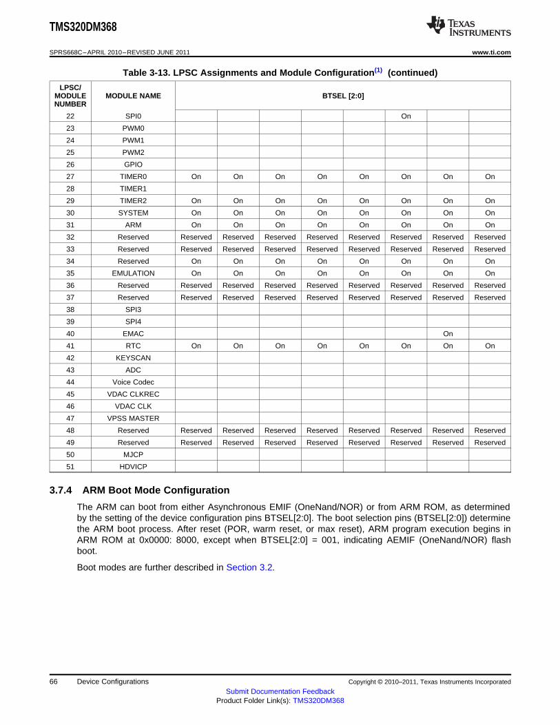
TMS320DM368
SPRS668C–APRIL 2010–REVISED JUNE 2011 www.ti.com
Table 3-13. LPSC Assignments and Module Configuration(1) (continued)
LPSC/MODULE MODULE NAME BTSEL [2:0]NUMBER
22 SPI0 On
23 PWM0
24 PWM1
25 PWM2
26 GPIO
27 TIMER0 On On On On On On On On
28 TIMER1
29 TIMER2 On On On On On On On On
30 SYSTEM On On On On On On On On
31 ARM On On On On On On On On
32 Reserved Reserved Reserved Reserved Reserved Reserved Reserved Reserved Reserved
33 Reserved Reserved Reserved Reserved Reserved Reserved Reserved Reserved Reserved
34 Reserved On On On On On On On On
35 EMULATION On On On On On On On On
36 Reserved Reserved Reserved Reserved Reserved Reserved Reserved Reserved Reserved
37 Reserved Reserved Reserved Reserved Reserved Reserved Reserved Reserved Reserved
38 SPI3
39 SPI4
40 EMAC On
41 RTC On On On On On On On On
42 KEYSCAN
43 ADC
44 Voice Codec
45 VDAC CLKREC
46 VDAC CLK
47 VPSS MASTER
48 Reserved Reserved Reserved Reserved Reserved Reserved Reserved Reserved Reserved
49 Reserved Reserved Reserved Reserved Reserved Reserved Reserved Reserved Reserved
50 MJCP
51 HDVICP
3.7.4 ARM Boot Mode Configuration
The ARM can boot from either Asynchronous EMIF (OneNand/NOR) or from ARM ROM, as determinedby the setting of the device configuration pins BTSEL[2:0]. The boot selection pins (BTSEL[2:0]) determinethe ARM boot process. After reset (POR, warm reset, or max reset), ARM program execution begins inARM ROM at 0x0000: 8000, except when BTSEL[2:0] = 001, indicating AEMIF (OneNand/NOR) flashboot.
Boot modes are further described in Section 3.2.
66 Device Configurations Copyright © 2010–2011, Texas Instruments Incorporated
Submit Documentation FeedbackProduct Folder Link(s): TMS320DM368

TMS320DM368
www.ti.com SPRS668C–APRIL 2010–REVISED JUNE 2011
3.7.5 AEMIF Configuration
3.7.5.1 AEMIF Pin Configuration
The input pins AECFG[2:0] determine the AEMIF configuration immediately after reset. Pins that are notassigned to another peripheral and not enabled as address signals become GPIOs. These may be usedas ALE and CLE signals for NAND Flash control if booting from internal ROM. If booting from NOR Flashthen the appropriate number of address output must be enabled by the AECFG[2:0] inputs at reset. Theenabled address signals are always contiguous from EM_BA[1] upwards; bits cannot be skipped. EM_A[0]does not represent the lowest AEMIF address bit. The device has 23 address lines and 2 chip selects withan 8-bit or 16-bit option. The device supports only 8-bit and 16-bit data widths for the AEMIF.
• 16-bit mode: EM_BA[1] represents the LS address bit (the half-word address) and EM_BA[0]represents address bit (A[14]). The maximum number of address lines pins in 16-bit mode are 23,which include EM_BA[1] + EM_A[0:13] +EM_BA[0] (as pin A[14] via PINMUX2 register) + EM_A[15:20]+EM_A[21] (via PINMUX4 register)Note: Pins EM_A[15:21] are available by programming the PinMux4 register in software after boot, butmust be pulled down externally so that valid voltage levels are provided on the full set of address pinsduring boot time. EM_A[15:21] come out of reset as GPIO pins per the PinMux4 register.
• 8-bit mode: EM_BA[1:0] represent the 2 LS address bits. Additional selections are available byprogramming the PinMux2 register in software after boot. The maximum number of address lines in8-bit mode are 23, which include EM_BA[0:1] + EM_A[0:13] + A[14] (via PINMUX4 register) +EM_A[15:20].Note: Pins EM_A[15:20] are available by programming the PinMux4 register in software after boot, butmust be pulled down externally so that valid voltage levels are provided on the full set of address pinsduring boot time. EM_A[15:20] come out of reset as GPIO pins per the PinMux4 register.
For additional details about the PinMux2 and PinMux4 registers, see the TMS320DM36x DMSoC ARMSubsystem Reference Guide (literature number SPRUFG5).
The device's pin-mux control logic allows all of the Asynchronous EMIF address pins to be used asGPIOs. If devices (such as NAND Flash) attached to the AEMIF require less than the 16 address pinsprovided, then the unused upper-order addresses may be configured as GPIOs. These pins must beconfigured at reset so that pins being driven by the AEMIF with addresses will not cause bus contentionwith pins being driven by the system as general purpose inputs.
The AECFG[2:0] value does not affect the operation of the AEMIF module itself, only which of its addressbits are seen on the device pins (resulting in the natural ramifications if devices don’t receive all addresssignals or if contention with general purpose inputs occurs). As shown in Table 3-14, the number ofaddress bits enabled on the AEMIF is selectable from 0 to 16 at boot time, see notes above for additionalsupport of up-to 23 address lines.
Copyright © 2010–2011, Texas Instruments Incorporated Device Configurations 67Submit Documentation Feedback
Product Folder Link(s): TMS320DM368
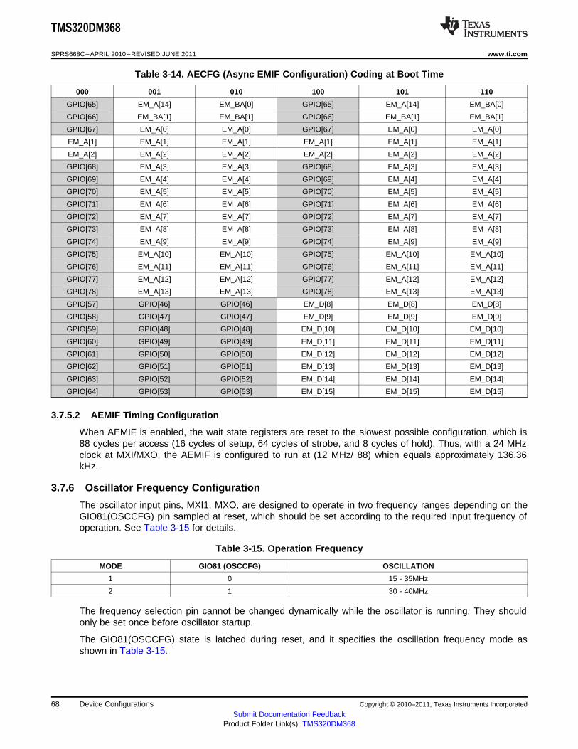
TMS320DM368
SPRS668C–APRIL 2010–REVISED JUNE 2011 www.ti.com
Table 3-14. AECFG (Async EMIF Configuration) Coding at Boot Time
000 001 010 100 101 110
GPIO[65] EM_A[14] EM_BA[0] GPIO[65] EM_A[14] EM_BA[0]
GPIO[66] EM_BA[1] EM_BA[1] GPIO[66] EM_BA[1] EM_BA[1]
GPIO[67] EM_A[0] EM_A[0] GPIO[67] EM_A[0] EM_A[0]
EM_A[1] EM_A[1] EM_A[1] EM_A[1] EM_A[1] EM_A[1]
EM_A[2] EM_A[2] EM_A[2] EM_A[2] EM_A[2] EM_A[2]
GPIO[68] EM_A[3] EM_A[3] GPIO[68] EM_A[3] EM_A[3]
GPIO[69] EM_A[4] EM_A[4] GPIO[69] EM_A[4] EM_A[4]
GPIO[70] EM_A[5] EM_A[5] GPIO[70] EM_A[5] EM_A[5]
GPIO[71] EM_A[6] EM_A[6] GPIO[71] EM_A[6] EM_A[6]
GPIO[72] EM_A[7] EM_A[7] GPIO[72] EM_A[7] EM_A[7]
GPIO[73] EM_A[8] EM_A[8] GPIO[73] EM_A[8] EM_A[8]
GPIO[74] EM_A[9] EM_A[9] GPIO[74] EM_A[9] EM_A[9]
GPIO[75] EM_A[10] EM_A[10] GPIO[75] EM_A[10] EM_A[10]
GPIO[76] EM_A[11] EM_A[11] GPIO[76] EM_A[11] EM_A[11]
GPIO[77] EM_A[12] EM_A[12] GPIO[77] EM_A[12] EM_A[12]
GPIO[78] EM_A[13] EM_A[13] GPIO[78] EM_A[13] EM_A[13]
GPIO[57] GPIO[46] GPIO[46] EM_D[8] EM_D[8] EM_D[8]
GPIO[58] GPIO[47] GPIO[47] EM_D[9] EM_D[9] EM_D[9]
GPIO[59] GPIO[48] GPIO[48] EM_D[10] EM_D[10] EM_D[10]
GPIO[60] GPIO[49] GPIO[49] EM_D[11] EM_D[11] EM_D[11]
GPIO[61] GPIO[50] GPIO[50] EM_D[12] EM_D[12] EM_D[12]
GPIO[62] GPIO[51] GPIO[51] EM_D[13] EM_D[13] EM_D[13]
GPIO[63] GPIO[52] GPIO[52] EM_D[14] EM_D[14] EM_D[14]
GPIO[64] GPIO[53] GPIO[53] EM_D[15] EM_D[15] EM_D[15]
3.7.5.2 AEMIF Timing Configuration
When AEMIF is enabled, the wait state registers are reset to the slowest possible configuration, which is88 cycles per access (16 cycles of setup, 64 cycles of strobe, and 8 cycles of hold). Thus, with a 24 MHzclock at MXI/MXO, the AEMIF is configured to run at (12 MHz/ 88) which equals approximately 136.36kHz.
3.7.6 Oscillator Frequency Configuration
The oscillator input pins, MXI1, MXO, are designed to operate in two frequency ranges depending on theGIO81(OSCCFG) pin sampled at reset, which should be set according to the required input frequency ofoperation. See Table 3-15 for details.
Table 3-15. Operation Frequency
MODE GIO81 (OSCCFG) OSCILLATION
1 0 15 - 35MHz
2 1 30 - 40MHz
The frequency selection pin cannot be changed dynamically while the oscillator is running. They shouldonly be set once before oscillator startup.
The GIO81(OSCCFG) state is latched during reset, and it specifies the oscillation frequency mode asshown in Table 3-15.
68 Device Configurations Copyright © 2010–2011, Texas Instruments Incorporated
Submit Documentation FeedbackProduct Folder Link(s): TMS320DM368

TMS320DM368
www.ti.com SPRS668C–APRIL 2010–REVISED JUNE 2011
3.8 Debugging Considerations
3.8.1 Pullup/Pulldown Resistors
Proper board design should ensure that input pins to the DMSoC device always be at a valid logic leveland not floating. This may be achieved via pullup/pulldown resistors. The DMSoC features internal pullup(IPU) and internal pulldown (IPD) resistors on most pins to eliminate the need, unless otherwise noted, forexternal pullup/pulldown resistors.
An external pullup/pulldown resistor needs to be used in the following situations:• Boot and Configuration Pins: If the pin is both routed out and 3-stated (not driven), an external
pullup/pulldown resistor is strongly recommended, even if the IPU/IPD matches the desiredvalue/state.
• Other Input Pins: If the IPU/IPD does not match the desired value/state, use an externalpullup/pulldown resistor to pull the signal to the opposite rail.
For the boot and configuration pins, if they are both routed out and 3-stated (not driven), it is stronglyrecommended that an external pullup/pulldown resistor be implemented. Although, internalpullup/pulldown resistors exist on these pins and they may match the desired configuration value,providing external connectivity can help ensure that valid logic levels are latched on these device boot andconfiguration pins. In addition, applying external pullup/pulldown resistors on the boot and configurationpins adds convenience to the user in debugging and flexibility in switching operating modes.
Tips for choosing an external pullup/pulldown resistor:• Consider the total amount of current that may pass through the pullup or pulldown resistor. Make sure
to include the leakage currents of all the devices connected to the net, as well as any internal pullup orpulldown resistors.
• Decide a target value for the net. For a pulldown resistor, this should be below the lowest VIL level ofall inputs connected to the net. For a pullup resistor, this should be above the highest VIH level of allinputs on the net. A reasonable choice would be to target the VOL or VOH levels for the logic family ofthe limiting device; which, by definition, have margin to the VIL and VIH levels.
• Select a pullup/pulldown resistor with the largest possible value; but, which can still ensure that the netwill reach the target pulled value when maximum current from all devices on the net is flowing throughthe resistor. The current to be considered includes leakage current plus, any other internal andexternal pullup/pulldown resistors on the net.
• For bidirectional nets, there is an additional consideration which sets a lower limit on the resistancevalue of the external resistor. Verify that the resistance is small enough that the weakest output buffercan drive the net to the opposite logic level (including margin).
• Remember to include tolerances when selecting the resistor value.• For pullup resistors, also remember to include tolerances on the DVDD rail.
For most systems, a 1-kΩ resistor can be used to oppose the IPU/IPD while meeting the above criteria.Users should confirm this resistor value is correct for their specific application.
For most systems, a 20-kΩ resistor can be used to compliment the IPU/IPD on the boot and configurationpins while meeting the above criteria. Users should confirm this resistor value is correct for their specificapplication.
For more detailed information on input current (II), and the low-/high-level input voltages (VIL and VIH) forthe device, see Section 5.2, Recommended Operating Conditions.
For the internal pullup/pulldown resistors for all device pins, see the peripheral/system-specific terminalfunctions table.
Copyright © 2010–2011, Texas Instruments Incorporated Device Configurations 69Submit Documentation Feedback
Product Folder Link(s): TMS320DM368

TMS320DM368
SPRS668C–APRIL 2010–REVISED JUNE 2011 www.ti.com
4 System Interconnect
The device uses a 64-bit crossbar architecture to control access between device processors, subsystemsand peripherals. There are eleven transfer masters (TCs have separate read and write connections)connected to the crossbar; ARM, the Video Processing Subsystem (VPSS), the master peripherals (USB,EMAC, HPI), and four EDMA transfer controllers. These can be connected to seven separate slave ports;ARM, the DDR EMIF, CFG bus peripherals, MJCP, and HDVICP. Not all masters may connect to allslaves. Connection paths are indicated by √ at intersection points shown in Table 4-1.
Table 4-1. System Connection Matrix
SLAVE MODULE
DMA ARM Internal MPEG/JPEG HD Video Image Config Bus Registers DDR EMIFMaster Memory Coprocessor Coprocessor and Memory
Memory Memory Memory
ARM √ √ √ √ √
VPSS √ √
DMA Master Peripherals √ √(USB, EMAC, HPI)
EDMA3TC0 √ √ √ √ √
EDMA3TC1 √ √ √ √ √
EDMA3TC2 √ √ √ √ √
EDMA3TC3 √ √ √ √ √
70 System Interconnect Copyright © 2010–2011, Texas Instruments Incorporated
Submit Documentation FeedbackProduct Folder Link(s): TMS320DM368

TMS320DM368
www.ti.com SPRS668C–APRIL 2010–REVISED JUNE 2011
5 Device Operating Conditions
5.1 Absolute Maximum Ratings Over Operating Case Temperature Range(Unless Otherwise Noted) (1) (2)
All 1.35-V supplies -0.3 V to 1.6 V
Supply voltage ranges All 1.8 V supplies -0.3 V to 2.45 V
All 3.3 V supplies -0.3 V to 3.8 V
All 1.8 V I/Os -0.5 V to 2.6 V
Input voltage ranges All 3.3 V I/Os -0.5 V to 3.8 V
USB_VBUS 0 V to 5.5 V
Commercial Temperature Tc 0°C to 85 °COperating case temperature ranges
Extended Temperature [D version devices] Tc -40°C to 85 °CStorage temperature ranges Tstg -55°C to 150°C
(1) Stresses beyond those listed under "absolute maximum ratings" may cause permanent damage to the device. These are stress ratingsonly, and functional operation of the device at these or any other conditions beyond those indicated under "recommended operatingconditions" is not implied. Exposure to absolute-maximum-rated conditions for extended periods may affect device reliability.
(2) All voltage values are with respect to VSS.
Copyright © 2010–2011, Texas Instruments Incorporated Device Operating Conditions 71Submit Documentation Feedback
Product Folder Link(s): TMS320DM368

TMS320DM368
SPRS668C–APRIL 2010–REVISED JUNE 2011 www.ti.com
5.2 Recommended Operating ConditionsNAME DESCRIPTION MIN NOM MAX UNIT
CVDD Core Supply Voltage 432-MHz devices 1.28 1.35 1.42 V
PRTCSS Oscillator andVDD12_PRTCSS 432-MHz devices 1.28 1.35 1.42 VPRTCSS Core Supply Voltage
VDDA12_DAC 1.2-V DAC Supply Voltage 432-MHz devices 1.28 1.35 1.42 V
VPP(1) VPP Supply Voltage 432-MHz devices 1.28 1.35 1.42 V
VDDS18 1.8-V Supply Voltage
VDD18_PRTCSS 1.8-V PWR CTRL Supply Voltage
VDDMXI 1.8-V System Oscillator Supply Voltage
VDD18_DDR 1.8-V DDR2 Supply Voltage
VDDA18_PLL 1.8-V PLL Supply Voltage1.71 1.8 1.89 V
VDDA18_USB 1.8-V USB Supply Voltage
VDDA18_VC 1.8-V Voice CODEC Supply Voltage
VDDA18_USB 1.8-V USB Supply VoltageSupplyVoltage VDDA18_ADC 1.8-V ADC Supply Voltage
VDDA18_DAC 1.8-V DAC Supply Voltage
VDD_AEMIF1_18_33 1.8/3.3-V switchable EMIF1 Supply Voltage
VDD_AEMIF2_18_33 1.8/3.3-V switchable EMIF2 Supply Voltage 1.71/3.14 1.8/3.3 1.89/3.46 V
VDD_ISIF18_33 1.8/3.3-V switchable ISIF Supply Voltage
VDDS33 3.3-V Supply Voltage
VDDA33_USB 3.3-V USB Supply Voltage 3.14 3.3 3.46 V
VDDA33_VC 3.3-V Voice CODEC Supply Voltage
VSS Core, USB Digital ground
VSS_MX1 OSC (MX1) ground (2)
VSS_32K OSC (32K) ground (2)
VSSA PLL ground (3)
VSSA18_USB USB groundSupply VSSA33_USB 3.3-V USB ground 0 0 0 VGround
VSSA33_VC 3.3-V Voice CODEC ground
VSSA18_VC 1.8-V Voice CODEC ground
VSSA_ADC ADC ground
VSSA18_DAC 1.8-V DAC ground
VSSA12_DAC 1.2-V DAC ground
High-level input voltage (4), excludes switchable I/O 2 V(3.3V I/O)Voltage Input VIHHigh High-level input voltage, non-DDR2 I/O, excludes switchable I/O 0.7VDDS18 V(1.8V I/O)
(1) For proper device operation, this pin must always be connected to CVDD.(2) Oscillator ground must be kept separate from other grounds and connected directly to the crystal load capacitor ground (see
Section 6.6.1).(3) For proper device operation, keep this pin separate from digital ground.(4) These I/O specifications apply to regular 3.3 V I/Os and do not apply to DDR2/mDDR, USB I/Os. DDR2/mDDR I/Os are 1.8 V I/Os and
adhere to JESD79-2A standard, USB I/Os adhere to USB2.0 spec.
72 Device Operating Conditions Copyright © 2010–2011, Texas Instruments Incorporated
Submit Documentation FeedbackProduct Folder Link(s): TMS320DM368

TMS320DM368
www.ti.com SPRS668C–APRIL 2010–REVISED JUNE 2011
NAME DESCRIPTION MIN NOM MAX UNIT
0.75*VDD1High-level input voltage I/O (1.35-V)VIH12RTC 2_PRTCS V(PWRCNT/PWRST/RTCXI/RTCXO) S
HIgh-level switchable input 3.3V I/O mode 2voltage (4)
(VDD_AEMIF1_18_33,VIH1833 VVDD_AEMIF2_18_33, 1.8V I/O mode 0.7VDDS18VDD_ISIF_18_33 poweredI/Os) (5) (6) (7) (8)
Low-level input voltage (4), excludes switchable I/O 0.8 V(3.3V I/O)VIL
Low-level input voltage (4), non-DDR2 I/O, excludes switchable I/O 0.3*VDDS V(1.8V I/O) 18
0.25*VDD1RTC Low-level input voltage (4)VIL12RTC 2_PRTCS VVoltage Input (1.35V I/O) SLow
Low-level switchable input 3.3V I/O mode 0.8voltage (4)
(VDD_AEMIF1_18_33,VIL1833 V0.3*VDDSVDD_AEMIF2_18_33, 1.8V I/O mode 18VDD_ISIF_18_33 poweredI/Os)
VREF DAC reference voltage 475 500 525 mV
RBIAS DAC full-scale current adjust resistor 2376 2400 2424 ΩHD 3CH DAC (9)
RLOAD_X Output resistor 74.25 75 75.75 Ω
CBG Bypass capacitor 0.1 uF
ROUT Output resistor (ROUT), between TVOUT and VFB pins 2128.5 2150 2171.5Ω
RFB Feedback resistor, between VFB and IDACOUT pins. 2079 2100 2121Video Buffer (9)
RBIAS Full-scale current adjust resistor 2400 Ω
CBG Bypass capacitor 0.1 uF
USB_VBUS USB external charge pump input 0 5.25 VUSB
VDDA12LDO_USB Internal LDO output (10) 0.22 µF
fs Sampling frequency 8 16 kHzVoice Codec
- System clock 256fs kHz
ADC FSCLK SCLK frequency 2 MHz
Default Temperature 0 85 °COperating case temperatureTemperature Tc Extended Temperature [D versionrange -40 85 °Cdevices]
(5) VDD_AEMIF1_18_33 : can be used as a power supply for EM_A[3:13], EM_BA0, EM_BA1, EM_CE[0], EM_ADV, EM_CLK,EM_D[8:15 ]pins, Keyscan, or GPIO pins.
(6) VDD_AEMIF2_18_33: can be used as a power supply for EM_A[0:2], EM_CE[1], EM_WE, EM_OE, EM_WAIT, EM_D[0:7] pins, HPI,Keyscan, or GPIO pins.
(7) Example 1: VDD_AEMIF2_18_33 at 1.8-V for 8-bit NAND VDD_AEMIF1_18_33 at 3.3-V for GPIO.Example 2: VDD_AEMIF1_18_33 and VDD_AEMIF2_18_33 at 1.8-V for 16-bit NAND.
(8) VDD_ISIF_18_33: can be used as a power supply for VPFE pins (CIN[7:0], YIN[7:0], C_WE_FIELD, PCLK), or SPI3(SPI3_SCLK,SPI3_SIMO,SPI3_SCS[0], SPI3_SCS[1]) or USBDRVVBUS or GPIO pins.
(9) See Section 6.12.2.4. Also, resistors should be E-96 spec line (3 digits with 1% accuracy).(10) For proper device operation, this pin must be connected to a 0.22μF capacitor to VDDA12LDO_USB.
Copyright © 2010–2011, Texas Instruments Incorporated Device Operating Conditions 73Submit Documentation Feedback
Product Folder Link(s): TMS320DM368

TMS320DM368
SPRS668C–APRIL 2010–REVISED JUNE 2011 www.ti.com
5.3 Electrical Characteristics Over Recommended Ranges of Supply Voltageand Operating Case Temperature (Unless Otherwise Noted)
PARAMETER TEST CONDITIONS (1) MIN TYP MAX UNIT
High-level output voltage VDDS33 = MIN, IOH = -2mA 2.4(3.3V I/O)
High-level output voltageVOH VDDS33 = MIN, IOH = -100μA 2.94 V(3.3V I/O)
High-level output voltage VDDS18 -VDDS18 = MIN, IOH = -2mA(1.8V I/O) 0.45VoltageOutput (2)
Low-level output voltage VDDS33 = MIN, IOL = 2mA 0.4(3.3V I/O)
Low-level output voltageVOL VDDS33 = MIN, IOL = 100μA 0.2 V(3.3V I/O)
Low-level output voltage VDDS18 = MIN, IOH = 2mA 0.45(1.8V I/O)
Input current for I/O withoutII VI = VSS to V DD ±10internal pull-up/pull-down
Input current for I/O withII(pullup) VI = VSS to VDD 100internal pull-up (3) (4)
Input current for I/O withCurrent II(pulldown) VI = VSS to VDD -100 μAinternal pull-down (3) (4)Input/Output
IOH High-level output current All peripherals -4000
IOL Low-level output current All peripherals 4000
VO = VDD or VSSIOZ(5) I/O off-state output current ±20(internal pull disabled)
CI Input capacitance 4Capacitance pF
CO Output capacitance 4
Resolution Resolution 10 Bits
RLOAD = 75 ΩINL Integral non-linearity, best fit -1.5 1.5 LSB(video buffer disabled)
RLOAD = 75 ΩDNL Differential non-linearity -1 1 LSB(video buffer disabled)HD 3CHDAC VOUT Output compliance range IFS = 6.67 mA, RLOAD = 75 Ω 0 VREF V
ZSET Zero Scale Offset Error 0.5 %
G_ERR Gain Error -5 5 %
Ch_match Channel matching +/-2 %
Output high voltageVOH(VIDBUF) 1.35(top of 75% NTSC or PAL colorbar)V
Output low voltageVOL(VIDBUF) 0.35Video Buffer (bottom of sync tip)
RES Resolution 10 bits
VOUT Output Voltage RLOAD = 75 Ω 0.35 1.35 V
(1) For test conditions shown as MIN, MAX, or NOM, use the appropriate value specified in the recommended operating conditions table.(2) These I/O specifications apply to regular 3.3 V and 1.8V I/Os and do not apply to DDR2/mDDR, USB I/Os. DDR2/mDDR I/Os are 1.8 V
I/Os and adhere to JESD79-2A standard, USB I/Os adhere to USB2.0 spec.(3) This specification applies only to pins with an internal pullup (PU) or pulldown (PD). See or Section 2.8 for pin descriptions.(4) To pull up a signal to the opposite supply rail, a 1 kΩ resistor is recommended.(5) IOZ applies to output only pins, indicating off-state (Hi-Z) output leakage current.
74 Device Operating Conditions Copyright © 2010–2011, Texas Instruments Incorporated
Submit Documentation FeedbackProduct Folder Link(s): TMS320DM368
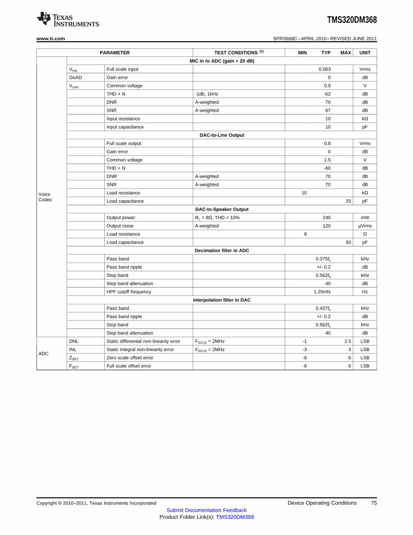
TMS320DM368
www.ti.com SPRS668C–APRIL 2010–REVISED JUNE 2011
PARAMETER TEST CONDITIONS (1) MIN TYP MAX UNIT
MIC in to ADC (gain = 20 dB)
Vmic Full scale input 0.063 Vrms
GeAD Gain error 0 dB
Vcom Common voltage 0.9 V
THD + N -1db, 1kHz -62 dB
DNR A-weighted 70 dB
SNR A-weighted 67 dB
Input resistance 10 kΩ
Input capacitance 10 pF
DAC-to-Line Output
Full scale output 0.8 Vrms
Gain error 0 dB
Common voltage 1.5 V
THD + N -60 dB
DNR A-weighted 70 dB
SNR A-weighted 70 dB
Load resistance 10 kΩVoiceCodec Load capacitance 20 pF
DAC-to-Speaker Output
Output power RL = 8Ω, THD = 10% 240 mW
Output noise A-weighted 120 μVrms
Load resistance 8 Ω
Load capacitance 50 pF
Decimation filter in ADC
Pass band 0.375fs kHz
Pass band ripple +/- 0.2 dB
Stop band 0.562fs kHz
Stop band attenuation 40 dB
HPF cutoff frequency 1.25mfs Hz
Interpolation filter in DAC
Pass band 0.437fs kHz
Pass band ripple +/- 0.2 dB
Stop band 0.562fs kHz
Stop band attenuation 40 dB
DNL Static differential non-linearity error FSCLK = 2MHz -1 2.5 LSB
INL Static integral non-linearity error FSCLK = 2MHz -3 3 LSBADC
ZSET Zero scale offset error -6 6 LSB
FSET Full scale offset error -6 6 LSB
Copyright © 2010–2011, Texas Instruments Incorporated Device Operating Conditions 75Submit Documentation Feedback
Product Folder Link(s): TMS320DM368

Transmission Line
4.0 pF 1.85 pF
Z0 = 50 Ω
(see note)
Tester Pin Electronics Data Sheet Timing Reference Point
OutputUnderTest
42 Ω 3.5 nH
Device Pin(see note)
Vref
Vref = VIL MAX (or VOL MAX)
Vref = VIH MIN (or VOH MIN)
TMS320DM368
SPRS668C–APRIL 2010–REVISED JUNE 2011 www.ti.com
6 Peripheral Information and Electrical Specifications
6.1 Parameter Information Device-Specific Information
A. The data sheet provides timing at the device pin. For output timing analysis, the tester pin electronics and itstransmission line effects must be taken into account. A model of the tester pin electronics is shown in Figure 6-1. Atransmission line with a delay of 2 ns or longer can be used to produce the desired transmission line effect. Thetransmission line is intended as a load only. It is not necessary to add or subtract the transmission line delay (2 ns orlonger) from the data sheet timings.Input requirements in this data sheet are tested with an input slew rate of < 4 Volts per nanosecond (4 V/ns) at thedevice pin and the input signals are driven between 0V and the appropriate I/O supply for the signal.
Figure 6-1. Test Load Circuit for AC Timing Measurements
The load capacitance value stated is only for characterization and measurement of AC timing signals. Thisload capacitance value does not indicate the maximum load the device is capable of driving.
6.1.1 Signal Transition Levels
All input and output timing parameters are referenced to Vref for both "0" and "1" logic levels. For 3.3 V I/O,Vref = 1.65 V. For 1.8 V I/O, Vref = 0.9 V.
Figure 6-2. Input and Output Voltage Reference Levels for AC Timing Measurements
All rise and fall transition timing parameters are referenced to VIL MAX and VIH MIN for input clocks,VOLMAX and VOH MIN for output clocks.
Figure 6-3. Rise and Fall Transition Time Voltage Reference Levels
6.1.2 Timing Parameters and Board Routing Analysis
The timing parameter values specified in this data sheet do not include delays by board routings. As agood board design practice, such delays must always be taken into account. Timing values may beadjusted by increasing/decreasing such delays. TI recommends utilizing the available I/O bufferinformation specification (IBIS) models to analyze the timing characteristics correctly. To properly use IBISmodels to attain accurate timing analysis for a given system, see the Using IBIS Models for TimingAnalysis Application Report (literature number SPRA839). If needed, external logic hardware such asbuffers may be used to compensate any timing differences.
76 Peripheral Information and Electrical Specifications Copyright © 2010–2011, Texas Instruments Incorporated
Submit Documentation FeedbackProduct Folder Link(s): TMS320DM368
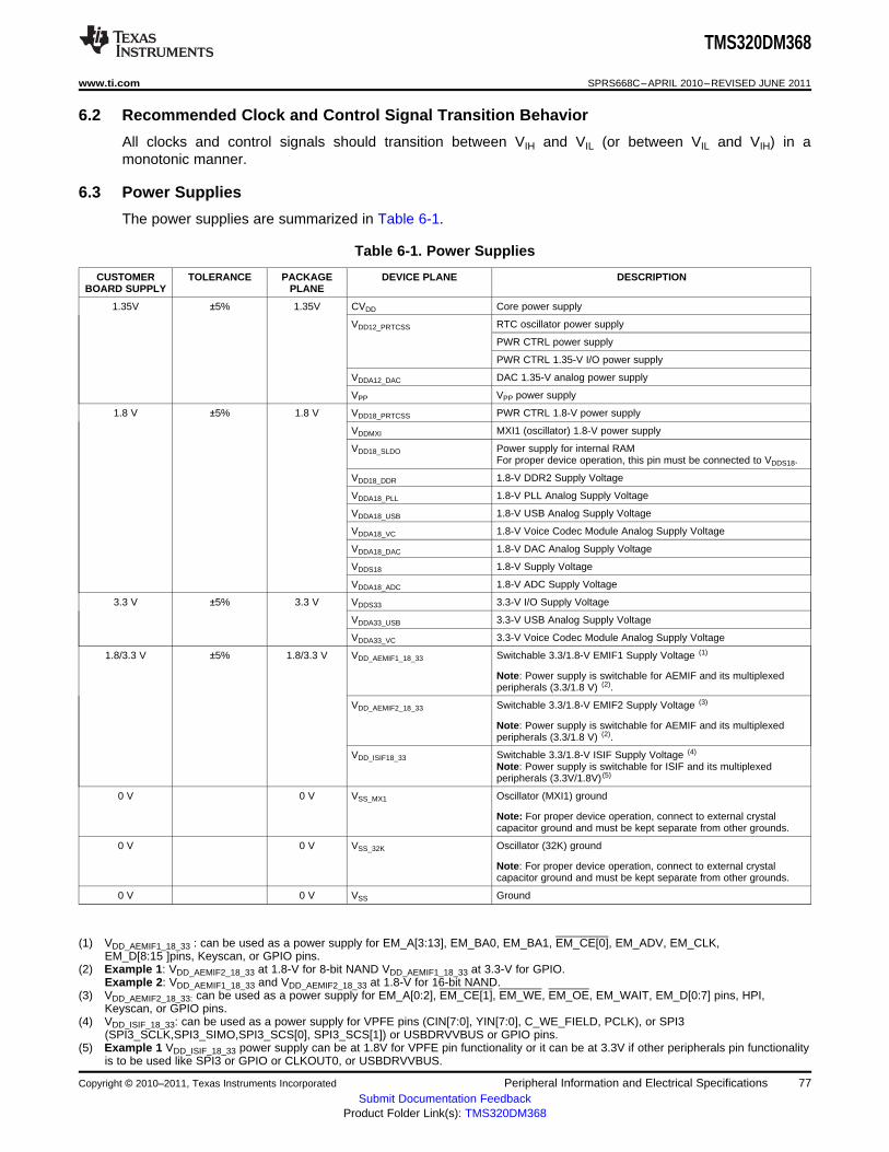
TMS320DM368
www.ti.com SPRS668C–APRIL 2010–REVISED JUNE 2011
6.2 Recommended Clock and Control Signal Transition Behavior
All clocks and control signals should transition between VIH and VIL (or between VIL and VIH) in amonotonic manner.
6.3 Power Supplies
The power supplies are summarized in Table 6-1.
Table 6-1. Power Supplies
CUSTOMER TOLERANCE PACKAGE DEVICE PLANE DESCRIPTIONBOARD SUPPLY PLANE
1.35V ±5% 1.35V CVDD Core power supply
VDD12_PRTCSS RTC oscillator power supply
PWR CTRL power supply
PWR CTRL 1.35-V I/O power supply
VDDA12_DAC DAC 1.35-V analog power supply
VPP VPP power supply
1.8 V ±5% 1.8 V VDD18_PRTCSS PWR CTRL 1.8-V power supply
VDDMXI MXI1 (oscillator) 1.8-V power supply
VDD18_SLDO Power supply for internal RAMFor proper device operation, this pin must be connected to VDDS18.
VDD18_DDR 1.8-V DDR2 Supply Voltage
VDDA18_PLL 1.8-V PLL Analog Supply Voltage
VDDA18_USB 1.8-V USB Analog Supply Voltage
VDDA18_VC 1.8-V Voice Codec Module Analog Supply Voltage
VDDA18_DAC 1.8-V DAC Analog Supply Voltage
VDDS18 1.8-V Supply Voltage
VDDA18_ADC 1.8-V ADC Supply Voltage
3.3 V ±5% 3.3 V VDDS33 3.3-V I/O Supply Voltage
VDDA33_USB 3.3-V USB Analog Supply Voltage
VDDA33_VC 3.3-V Voice Codec Module Analog Supply Voltage
1.8/3.3 V ±5% 1.8/3.3 V VDD_AEMIF1_18_33 Switchable 3.3/1.8-V EMIF1 Supply Voltage (1)
Note: Power supply is switchable for AEMIF and its multiplexedperipherals (3.3/1.8 V) (2).
VDD_AEMIF2_18_33 Switchable 3.3/1.8-V EMIF2 Supply Voltage (3)
Note: Power supply is switchable for AEMIF and its multiplexedperipherals (3.3/1.8 V) (2).
VDD_ISIF18_33 Switchable 3.3/1.8-V ISIF Supply Voltage (4)
Note: Power supply is switchable for ISIF and its multiplexedperipherals (3.3V/1.8V) (5)
0 V 0 V VSS_MX1 Oscillator (MXI1) ground
Note: For proper device operation, connect to external crystalcapacitor ground and must be kept separate from other grounds.
0 V 0 V VSS_32K Oscillator (32K) ground
Note: For proper device operation, connect to external crystalcapacitor ground and must be kept separate from other grounds.
0 V 0 V VSS Ground
(1) VDD_AEMIF1_18_33 : can be used as a power supply for EM_A[3:13], EM_BA0, EM_BA1, EM_CE[0], EM_ADV, EM_CLK,EM_D[8:15 ]pins, Keyscan, or GPIO pins.
(2) Example 1: VDD_AEMIF2_18_33 at 1.8-V for 8-bit NAND VDD_AEMIF1_18_33 at 3.3-V for GPIO.Example 2: VDD_AEMIF1_18_33 and VDD_AEMIF2_18_33 at 1.8-V for 16-bit NAND.
(3) VDD_AEMIF2_18_33: can be used as a power supply for EM_A[0:2], EM_CE[1], EM_WE, EM_OE, EM_WAIT, EM_D[0:7] pins, HPI,Keyscan, or GPIO pins.
(4) VDD_ISIF_18_33: can be used as a power supply for VPFE pins (CIN[7:0], YIN[7:0], C_WE_FIELD, PCLK), or SPI3(SPI3_SCLK,SPI3_SIMO,SPI3_SCS[0], SPI3_SCS[1]) or USBDRVVBUS or GPIO pins.
(5) Example 1 VDD_ISIF_18_33 power supply can be at 1.8V for VPFE pin functionality or it can be at 3.3V if other peripherals pin functionalityis to be used like SPI3 or GPIO or CLKOUT0, or USBDRVVBUS.
Copyright © 2010–2011, Texas Instruments Incorporated Peripheral Information and Electrical Specifications 77Submit Documentation Feedback
Product Folder Link(s): TMS320DM368
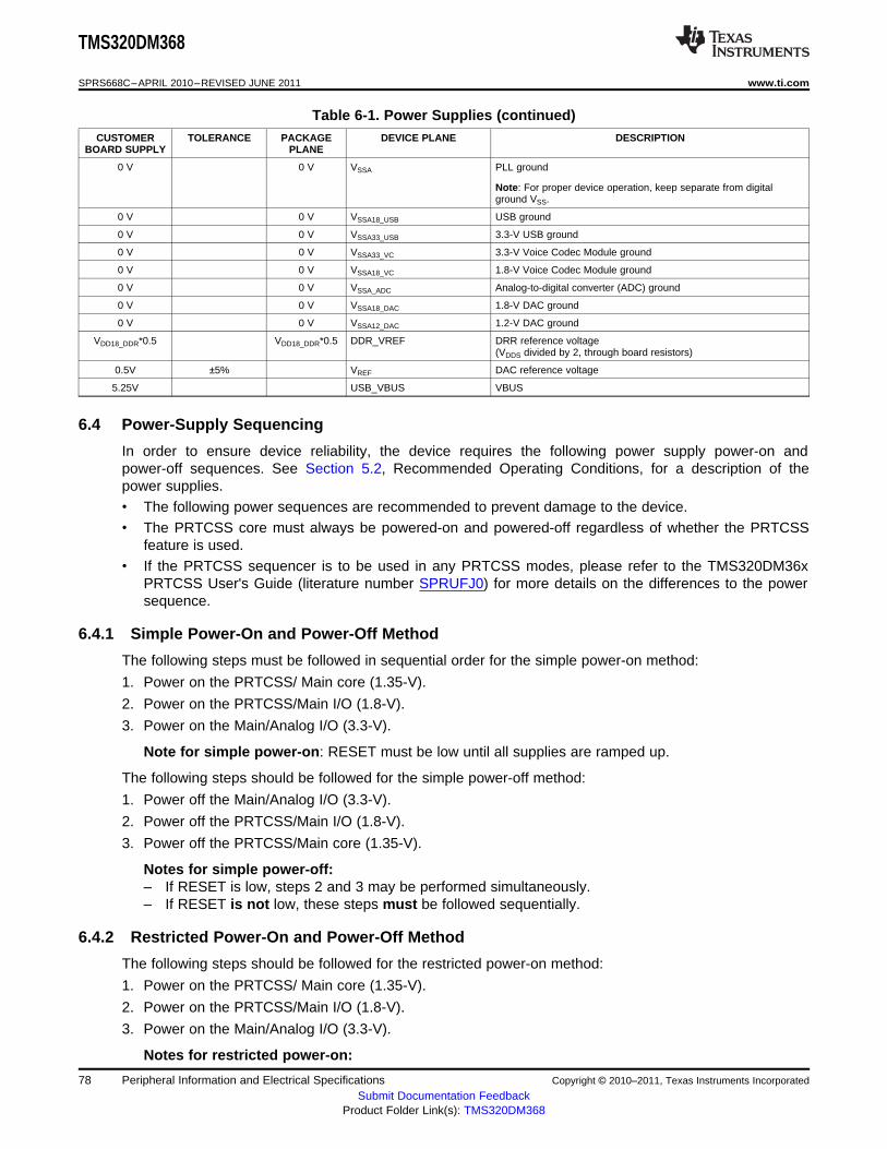
TMS320DM368
SPRS668C–APRIL 2010–REVISED JUNE 2011 www.ti.com
Table 6-1. Power Supplies (continued)CUSTOMER TOLERANCE PACKAGE DEVICE PLANE DESCRIPTION
BOARD SUPPLY PLANE
0 V 0 V VSSA PLL ground
Note: For proper device operation, keep separate from digitalground VSS.
0 V 0 V VSSA18_USB USB ground
0 V 0 V VSSA33_USB 3.3-V USB ground
0 V 0 V VSSA33_VC 3.3-V Voice Codec Module ground
0 V 0 V VSSA18_VC 1.8-V Voice Codec Module ground
0 V 0 V VSSA_ADC Analog-to-digital converter (ADC) ground
0 V 0 V VSSA18_DAC 1.8-V DAC ground
0 V 0 V VSSA12_DAC 1.2-V DAC ground
VDD18_DDR*0.5 VDD18_DDR*0.5 DDR_VREF DRR reference voltage(VDDS divided by 2, through board resistors)
0.5V ±5% VREF DAC reference voltage
5.25V USB_VBUS VBUS
6.4 Power-Supply Sequencing
In order to ensure device reliability, the device requires the following power supply power-on andpower-off sequences. See Section 5.2, Recommended Operating Conditions, for a description of thepower supplies.• The following power sequences are recommended to prevent damage to the device.• The PRTCSS core must always be powered-on and powered-off regardless of whether the PRTCSS
feature is used.• If the PRTCSS sequencer is to be used in any PRTCSS modes, please refer to the TMS320DM36x
PRTCSS User's Guide (literature number SPRUFJ0) for more details on the differences to the powersequence.
6.4.1 Simple Power-On and Power-Off Method
The following steps must be followed in sequential order for the simple power-on method:
1. Power on the PRTCSS/ Main core (1.35-V).
2. Power on the PRTCSS/Main I/O (1.8-V).
3. Power on the Main/Analog I/O (3.3-V).
Note for simple power-on: RESET must be low until all supplies are ramped up.
The following steps should be followed for the simple power-off method:
1. Power off the Main/Analog I/O (3.3-V).
2. Power off the PRTCSS/Main I/O (1.8-V).
3. Power off the PRTCSS/Main core (1.35-V).
Notes for simple power-off:– If RESET is low, steps 2 and 3 may be performed simultaneously.– If RESET is not low, these steps must be followed sequentially.
6.4.2 Restricted Power-On and Power-Off Method
The following steps should be followed for the restricted power-on method:
1. Power on the PRTCSS/ Main core (1.35-V).
2. Power on the PRTCSS/Main I/O (1.8-V).
3. Power on the Main/Analog I/O (3.3-V).
Notes for restricted power-on:
78 Peripheral Information and Electrical Specifications Copyright © 2010–2011, Texas Instruments Incorporated
Submit Documentation FeedbackProduct Folder Link(s): TMS320DM368

TMS320DM368
www.ti.com SPRS668C–APRIL 2010–REVISED JUNE 2011
– RESET must be low until all supplies are ramped up.– Steps 1, 2, and 3 may be performed simultaneously if the Main core finishes ramping up before the
I/Os and the maximum delta voltage difference between the 1.8-V and 3.3-V I/Os is 2.0-V until the1.8-V I/O reaches the full voltage.
The following steps should be followed for the restricted power-off method:
1. Power off Main/Analog I/O (3.3-V).
2. Power off PRTCSS/Main I/O (1.8-V).
3. Power off PRTCSS/Main core (1.35-V).
Notes for restricted power-off:– The 3.3-/1.8-V I/Os may be powered off simultaneously if the maximum delta voltage difference
between them is 2.0V until the 1.8-V I/O is completely powered off, and the PRTCSS/Main coremust be powered down last.
When booting the DM368 from OneNAND, you must ensure that the OneNAND device is ready with validprogram instructions before the DM368 attempts to read program instructions from it. In particular, beforeyou release the device's reset, you must allow time for OneNAND device power to stabilize and for theOneNAND device to complete its internal copy routine. During the internal copy routine, the OneNANDdevice copies boot code from its internal non-volatile memory to its internal boot memory section. Boarddesigners typically achieve this requirement by design of the system power and reset supervisor circuit.Refer to your OneNAND device datasheet for OneNAND power ramp and stabilization times and forOneNAND boot copy times.
6.4.3 Power-Supply Design Considerations
Core and I/O supply voltage regulators should be located close to the device to minimize inductance andresistance in the power delivery path. Additionally, when designing for high-performance applicationsutilizing the device, the PC board should include separate power planes for core, I/O, and ground, allbypassed with high-quality low-ESL/ESR capacitors.
6.4.4 Power-Supply Decoupling
In order to properly decouple the supply planes from system noise, place as many capacitors (caps) aspossible close to the device. These caps need to be close to the power pins, no more than 1.25 cmmaximum distance to be effective. Physically smaller caps, such as 0402, are better because of theirlower parasitic inductance. Proper capacitance values are also important. Small bypass caps (near 560pF) should be closest to the power pins. Medium bypass caps (220 nF or as large as can be obtained in asmall package) should be next closest. TI recommends no less than 8 small and 8 medium caps persupply be placed immediately next to the BGA vias, using the "interior" BGA space and at least thecorners of the "exterior".
Larger caps for each supply can be placed further away for bulk decoupling. Large bulk caps (on the orderof 100 uF) should be furthest away, but still as close as possible. Large caps for each supply should beplaced outside of the BGA footprint.
Any cap selection needs to be evaluated from a yield/manufacturing point-of-view. As with the selection ofany component, verification of capacitor availability over the product’s production lifetime should beconsidered. See also Section 6.6.1 for additional recommendations on power supplies for theoscillator/PLL supplies.
Copyright © 2010–2011, Texas Instruments Incorporated Peripheral Information and Electrical Specifications 79Submit Documentation Feedback
Product Folder Link(s): TMS320DM368
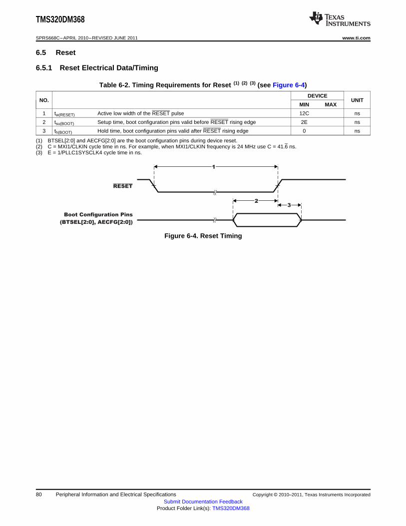
1
23
RESET
Boot Configuration Pins
(BTSEL[2:0], AECFG[2:0])
TMS320DM368
SPRS668C–APRIL 2010–REVISED JUNE 2011 www.ti.com
6.5 Reset
6.5.1 Reset Electrical Data/Timing
Table 6-2. Timing Requirements for Reset (1) (2) (3) (see Figure 6-4)
DEVICENO. UNIT
MIN MAX
1 tw(RESET) Active low width of the RESET pulse 12C ns
2 tsu(BOOT) Setup time, boot configuration pins valid before RESET rising edge 2E ns
3 th(BOOT) Hold time, boot configuration pins valid after RESET rising edge 0 ns
(1) BTSEL[2:0] and AECFG[2:0] are the boot configuration pins during device reset.(2) C = MXI1/CLKIN cycle time in ns. For example, when MXI1/CLKIN frequency is 24 MHz use C = 41.6 ns.(3) E = 1/PLLC1SYSCLK4 cycle time in ns.
Figure 6-4. Reset Timing
80 Peripheral Information and Electrical Specifications Copyright © 2010–2011, Texas Instruments Incorporated
Submit Documentation FeedbackProduct Folder Link(s): TMS320DM368

C1 C2
MXI1/CLKIN MXO1 VSS_MX1
0.1 Fµ
L1
VDDA_PLL1 VSSA_PLL1
Crystal19.2 MHz24 MHz or
36 MHz
0.1 Fµ
CL
C1C2
(C1 C2)
TMS320DM368
www.ti.com SPRS668C–APRIL 2010–REVISED JUNE 2011
6.6 Oscillators and Clocks
The device has one oscillator input/output pair (MXI1/MXO1) usable with external crystals or ceramicresonators to provide clock inputs. The optimal frequencies for the crystals are 19.2 MHz, 24 MHz, 27MHz, and 36 MHz. Optionally, the oscillator inputs are configurable for use with external clock oscillators.If external clock oscillators are used, to minimize the clock jitter, a single clean power supply should powerboth the device and the external oscillator circuit and the minimum CLKIN rise and fall times must beobserved. The electrical requirements and characteristics are described in this section.
The timing parameters for CLKOUT[3:1] are also described in this section. The device has three outputclock pins (CLKOUT[3:1]). See Section 3.3 for more information on CLKOUT[3:1].
Note: Please ensure that the appropriate oscillator input pin (GIO81/OSCCFG) frequency range setting isset correctly. For more details on this pin setting, see Section 3.7.6.
6.6.1 MXI1 Oscillator
The MXI1 (typically 24 MHz, can also be 19.2 MHz, 27 MHz, or 36 MHz) oscillator provides the primaryreference clock for the device. The on-chip oscillator requires an external crystal connected across theMXI1 and MXO1 pins, along with two load capacitors, as shown in Figure 6-5. The external crystal loadcapacitors must be connected only to the oscillator ground pin (VSS_MX1). Do not connect to board ground(VSS). Also, the PLL power pin (VDDA_PLL1) should be connected to the power supply through a ferritebead, L1 in the example circuit shown in Figure 6-5.
Note: If an external oscillator is to be used, the external oscillator clock signal should be connected to theMXI1 pin with a 1.8V amplitude. The MXO1 should be left unconnected and the VSS_MX1 signal shouldbe connected to board ground (Vss).
Figure 6-5. MXI1 Oscillator
The load capacitors, C1 and C2, should be chosen such that the equation is satisfied (typical values areC1 = C2 = 10 pF). CL in the equation is the load specified by the crystal manufacturer. All discretecomponents used to implement the oscillator circuit should be placed as close as possible to theassociated oscillator pins (MXI1 and MXO1) and to the VSS_MX1 pin.
Copyright © 2010–2011, Texas Instruments Incorporated Peripheral Information and Electrical Specifications 81Submit Documentation Feedback
Product Folder Link(s): TMS320DM368

MXI1/CLKIN
2
3
4
4
5 1
TMS320DM368
SPRS668C–APRIL 2010–REVISED JUNE 2011 www.ti.com
Table 6-3. Switching Characteristics Over Recommended Operating Conditions for System Oscillator
PARAMETER MIN TYP MAX UNIT
Start-up time (from power up until oscillating at stable frequency) 2 ms
Oscillation frequency 19.2/24/2 MHz7/36
Crystal ESR 19 - 30 MHz 60 Ω30 - 36 MHz 40 Ω
Frequency stability +/-50 ppm
6.6.2 Clock PLL Electrical Data/Timing (Input and Output Clocks)
Table 6-4. Timing Requirements for MXI1/CLKIN1 (1) (2) (3) (see Figure 6-6)
DEVICENO UNIT. MIN TYP MAX
1 tc(MXI1) Cycle time, MXI1/CLKIN1 27.7 52.083 ns
2 tw(MXI1H) Pulse duration, MXI1/CLKIN1 high 0.45C 0.55C ns
3 tw(MXI1L) Pulse duration, MXI1/CLKIN1 low 0.45C 0.55C ns
4 tt(MXI1) Transition time, MXI1/CLKIN1 .05C ns
5 tJ(MXI1) Period jitter, MXI1/CLKIN1 .02C ns
(1) The reference points for the rise and fall transitions are measured at VIL MAX and VIH MIN.(2) C = MXI1/CLKIN1 cycle time in ns. For example, when MXI1/CLKIN1 frequency is 24 MHz use C = 41.6 ns.(3) tc(MXI1) = 52.083 ns, tc(MXI1) = 41.6 ns, tc(MXI1) = 37.037 ns, and tc(MXI1) = 27.7 ns are the only supported cycle times for
MXI1/CLKIN1.
Figure 6-6. MXI1/CLKIN1 Timing
82 Peripheral Information and Electrical Specifications Copyright © 2010–2011, Texas Instruments Incorporated
Submit Documentation FeedbackProduct Folder Link(s): TMS320DM368

CLKOUT0/1
1
24
4
MXI1/CLKIN
5 6
3
MXI1/CLKIN
CLKOUT2
12
3
4
56
4
TMS320DM368
www.ti.com SPRS668C–APRIL 2010–REVISED JUNE 2011
Table 6-5. Switching Characteristics Over Recommended Operating Conditions for CLKOUT0/CLKOUT1 (1)(2) (see Figure 6-7)
DEVICENO. PARAMETER UNIT
MIN TYP MAX
1 tC(CLKOUT0/CLKOUT1) Cycle time, CLKOUT0/CLKOUT1 27.7 ns
2 tw(CLKOUT0H/CLKOUT1H) Pulse duration, CLKOUT0/CLKOUT1 high .45P .55P ns
3 tw(CLKOUT0L/CLKOUT1L) Pulse duration, CLKOUT0/CLKOUT1 low .45P .55P ns
4 tt(CLKOUT0/CLKOUT1) Transition time, CLKOUT0/CLKOUT1 3 ns
Delay time, MXI1/CLKIN1 high to CLKOUT0/CLKOUT15 td(MXI1H-CLKOUT0H/CLKOUT1H) 1 8 nshigh
Delay time, MXI1/CLKIN1I low to CLKOUT0/CLKOUT16 td(MXI1L-CLKOUT0L/CLKOUT1L) 1 8 nslow
(1) The reference points for the rise and fall transitions are measured at VOL MAX and VOHMIN.(2) P = 1/CLKOUT0/1 clock frequency in nanoseconds (ns). For example, when CLKOUT1 frequency is 24 MHz use P = 41.6 ns.
Figure 6-7. CLKOUT1 Timing
Table 6-6. Switching Characteristics Over Recommended Operating Conditions for CLKOUT2 (1) (2) (seeFigure 6-8)
DEVICENO. PARAMETER UNIT
MIN TYP MAX
1 tC(CLKOUT2) Cycle time, CLKOUT2 20 ns
2 tw(CLKOUT2H) Pulse duration, CLKOUT2 high .45P .55P ns
3 tw(CLKOUT2L) Pulse duration, CLKOUT2 low .45P .55P ns
4 tt(CLKOUT2) Transition time, CLKOUT2 3 ns
td(MXI1H-5 Delay time, MXI1/CLKIN1 high to CLKOUT2 high 1 8 nsCLKOUT2H)
td(MXI1L-6 Delay time, MXI1/CLKIN1 low to CLKOUT2 low 1 8 nsCLKOUT2L)
(1) The reference points for the rise and fall transitions are measured at VOL MAX and VOH MIN.(2) P = 1/CLKOUT2 clock frequency in nanoseconds (ns). For example, when CLKOUT2 frequency is 8 MHz use P = 125 ns.
Figure 6-8. CLKOUT2 Timing
Copyright © 2010–2011, Texas Instruments Incorporated Peripheral Information and Electrical Specifications 83Submit Documentation Feedback
Product Folder Link(s): TMS320DM368
C1 C2
RTCXI RTCXO VSS_32k
Crystal32.768 kHz
CL
C1C2
(C1 C2)
RTCXI
2
3
1
TMS320DM368
SPRS668C–APRIL 2010–REVISED JUNE 2011 www.ti.com
6.6.3 PRTCSS Oscillator
The device has an PRTCSS oscillator input/output pair (RTCXI/RTCXO) usable with external crystals orceramic resonators to provide clock inputs. The optimal frequency for the crystal is 32.768 kHz. Theelectrical requirements and characteristics are described in this section. Figure 6-9 shows an examplecircuit.
Figure 6-9. RTCXI1 Oscillator
The load capacitors, C1 and C2, should be chosen such that the equation is satisfied (typical values areC1 = C2 = 2 fF). CL in the equation below is the load specified by the crystal manufacturer. All discretecomponents used to implement the oscillator circuit should be placed as close as possible to theassociated oscillator pins (RTCXI and RTCXO) and to the VSS_32K pin.
(1)
6.6.4 PRTCSS Electrical Data/Timing
Table 6-7. Timing Requirements for RTCXI (1) (2) (see Figure 6-6)
DEVICE UNITNO.
MIN TYP MAX
1 tc(RTCXI) Cycle time, RTCXI 30.5175 µs
2 tw(RTCXIH) Pulse duration, RTCXI high .45C .55C ns
3 tw(RTCXIL) Pulse duration, RTCXI low .45C .55C ns
(1) The reference points for the rise and fall transitions are measured at VIL MAX and VIH MIN.(2) C = MXI1/CLKIN1 cycle time in ns. For example, when MXI1/CLKIN1 frequency is 24 MHz use C = 41.6 ns.
Figure 6-10. RTCXI Timing
84 Peripheral Information and Electrical Specifications Copyright © 2010–2011, Texas Instruments Incorporated
Submit Documentation FeedbackProduct Folder Link(s): TMS320DM368

TMS320DM368
www.ti.com SPRS668C–APRIL 2010–REVISED JUNE 2011
Table 6-8. Switching Characteristics Over Recommended Operating Conditions for RTC Oscillator
PARAMETER MIN TYP MAX UNIT
Start-up time (from power up until oscillating at stable frequency) 0.85 2 s
Oscillation frequency 32.768 kHz
Crystal ESR 70 kΩFrequency stability +/- 50 ppm
The load capacitors, C1 and C2, should be chosen such that the equation is satisfied (typical values areC1 = C2 = 2 fF). CL in the equation is the load specified by the crystal manufacturer. All discretecomponents used to implement the oscillator circuit should be placed as close as possible to theassociated oscillator pins (RTCXI and RTCXO) and to the VSS_MX1 pin.
6.7 Power Management and Real Time Clock Subsystem (PRTCSS)
The Power Management and Real Time Clock Subsystem (PRTCSS) is used for calendar applications.The PRTCSS has an independent power supply and can remain ON while the rest of the power supply isturned OFF. The PRTCSS supports the following features:• Real Time Clock (RTC)
– Simple day counter (Up to 89-years)– To generate the Alarm event to check the RTC count– 16-bit simple timer– Watch-dog timer to generate the event for RTC-Sequencer
• General Purpose I/O with Anti-chattering– 3-output pins (PWRCTRO[2:0])– 7-In/Output pins (PWRCTRIO[6:0])
• Interrupt– 2 RTCSS interrupts (ARMSS and Timer)– 7 GPIO interrupts (PWRCTRIO[6:0]
6.7.1 PRTCSS Peripheral Register Description(s)
The following table lists the PRTCSS Interface registers (PRTCIF) and Table 6-10 lists the PRTCSSregisters which can only be accessed via the PRTCIF registers, their corresponding acronyms, and devicememory locations (offsets). For more details, see the TMS320DM36x PRTCSS User's Guide (literaturenumber SPRUFJ0).
Table 6-9. PRTC Interface (PRTCIF) Registers
Offset Acronym Register Description
0x0 PID PRTCIF peripheral ID register
0x4 PRTCIF_CTRL PRTCIF control register
0x8 PRTCIF_LDATA PRTCIF access lower data register
0xC PRTCIF_UDATA PRTCIF access upper data register
0x10 PRTCIF_INTEN PRTCIF interrupt enable register
0x14 PRTCIF_INTFLG PRTCIF interrupt flag register
Table 6-10. Power Management and Real Time Clock Subsystem (PRTCSS) Registers
Offset Acronym Register Description
0x0 GO_OUT Global output pin output data register
0x1 GIO_OUT Global input/output pin output data register
0x2 GIO_DIR Global input/output pin direction register
0x3 GIO_IN Global input/output pin input data register
Copyright © 2010–2011, Texas Instruments Incorporated Peripheral Information and Electrical Specifications 85Submit Documentation Feedback
Product Folder Link(s): TMS320DM368

TMS320DM368
SPRS668C–APRIL 2010–REVISED JUNE 2011 www.ti.com
Table 6-10. Power Management and Real Time Clock Subsystem (PRTCSS) Registers (continued)
Offset Acronym Register Description
0x4 GIO_FUNC Global input/output pin function register
0x5 GIO_RISE_INT_EN GIO rise interrupt enable register
0x6 GIO_FALL_INT_EN GIO fall interrupt enable register
0x7 GIO_RISE_INT_FLG GIO rise interrupt flag register
0x8 GIO_FALL_INT_FLG GIO fall interrupt flag register
0x9 - 0xA Reserved Reserved
0xB INTC_EXTENA0 EXT interrupt enable 0 register
0xC INTC_EXTENA1 EXT interrupt enable 1 register
0xD INTC_FLG0 Event interrupt flag 0 register
0xE INTC_FLG1 Event interrupt flag 1 register
0x10 RTC_CTRL RTC control register
0x11 RTC_WDT Watchdog timer counter register
0x12 RTC_TMR0 Timer counter 0 register
0x13 RTC_TMR1 Timer counter 1 register
0x14 RTC_CCTRL Calender control register
0x15 RTC_SEC Seconds register
0x16 RTC_MIN Minutes register
0x17 RTC_HOUR Hours register
0x18 RTC_DAY0 Days[[7:0] register
0x19 RTC_DAY1 Days[14:8] register
0x1A RTC_AMIN Minutes Alarm register
0x1B RTC_AHOUR Hour Alarm register
0x1C RTC_ADAY0 Days[7:0] Alarm register
0x1D RTC_ADAY1 Days[14:8] Alarm register
0x20 CLKC_CNT Clock control register
86 Peripheral Information and Electrical Specifications Copyright © 2010–2011, Texas Instruments Incorporated
Submit Documentation FeedbackProduct Folder Link(s): TMS320DM368
TMS320DM368
www.ti.com SPRS668C–APRIL 2010–REVISED JUNE 2011
6.8 General-Purpose Input/Output (GPIO)
The GPIO peripheral provides general-purpose pins that can be configured as either inputs or outputs.When configured as an output, a write to an internal register can control the state driven on the output pin.When configured as an input, the state of the input is detectable by reading the state of an internalregister. In addition, the GPIO peripheral can produce CPU interrupts and EDMA events in differentinterrupt/event generation modes. The GPIO peripheral provides generic connections to external devices.The GPIO pins are grouped into banks of 16 pins per bank (i.e., bank 0 consists of GPIO [0:15]). Thereare a total of 7 GPIO banks in the device, because the device has 104 GPIOs. For additional details onGPIO pins voltage level and the associated power supply please see Table 6-11.
Table 6-11. GPIO Pin Voltage Level and Power Supply Reference
Voltage Level 1.8 V or 3.3 V 3.3 V 1.8 V
Power Supply Name VDD_AEMIF1_18_33 VDD_AEMIF2_18_33 VDD_ISIF18_33 VDDS33 VDD18_PRTCSS
GIO[78:68] GIO[67] GIO[103:93] GIO[92:79] GIO[110:104]
Pin Name GIO[66:56] GIO[55:52] GIO[49:0]
GIO[51:50]
The GPIO peripheral supports the following:• Up to 104 GPIO pins, GPIO[103:0]• Up to 7 GPIO pins dedicated to the PRTC Subsystem. These pins are labeled as PWRCTRIO[6:0].
Only PWRCTRIO[2:0] are connected to the GPIO module, labeled as GPIO[106:104]. For the PRTCSSmodule the PWRCTRIO[6:0] pins support input and output functionality but for the GPIO module theGPIO[106:104] pins support input functionality only. For more details please refer to Section 6.7.
• Interrupts:– Up to 15 unique GPIO[15:0] interrupts from Bank 0.– Up to 3 unique GPIO[106:104] interrupts from Bank 6, dedicated to the PRTC Subsystem. For
more details please refer to Section 6.7.– Interrupts can be triggered by rising and/or falling edge, specified for each interrupt capable GPIO
signal• DMA events:
– Up to 15 unique GPIO DMA events from Bank 0• Set/clear functionality: Firmware writes 1 to corresponding bit position(s) to set or to clear GPIO
signal(s). This allows multiple firmware processes to toggle GPIO output signals without critical sectionprotection (disable interrupts, program GPIO, re-enable interrupts, to prevent context switching toanther process during GPIO programming).
• Separate Input/Output registers• Output register in addition to set/clear so that, if preferred by firmware, some GPIO output signals can
be toggled by direct write to the output register(s).• Output register, when read, reflects output drive status. This, in addition to the input register reflecting
pin status, allows wired logic be implemented.
For more detailed information on GPIOs, see the Documentation Support section for the General-PurposeInput/Output (GPIO) Reference Guide.
Copyright © 2010–2011, Texas Instruments Incorporated Peripheral Information and Electrical Specifications 87Submit Documentation Feedback
Product Folder Link(s): TMS320DM368

TMS320DM368
SPRS668C–APRIL 2010–REVISED JUNE 2011 www.ti.com
6.8.1 GPIO Peripheral Register Description(s)
Table 6-12 lists the GPIO registers, their corresponding acronyms, and device memory locations (offsets).
Table 6-12. General-Purpose Input/Output (GPIO) Registers
OFFSET ACRONYM REGISTER DESCRIPTION
0h PID Peripheral Identification Register
8h BINTEN GPIO Interrupt Per-Bank Enable Register
GPIO Banks 0 and 1
10h DIR01 GPIO Banks 0 and 1 Direction Register
14h OUT_DATA01 GPIO Banks 0 and 1 Output Data Register
18h SET_DATA01 GPIO Banks 0 and 1 Set Data Register
1Ch CLR_DATA01 GPIO Banks 0 and 1 Clear Data Register
20h IN_DATA01 GPIO Banks 0 and 1 Input Data Register
24h SET_RIS_TRIG GPIO Set Rising Edge Interrupt Register
28h CLR_RIS_TRIG GPIO Clear Rising Edge Interrupt Register
2Ch SET_FAL_TRIG GPIO Set Falling Edge Interrupt Register
30h CLR_FAL_TRIG GPIO Clear Falling Edge Interrupt Register
34h INTSTAT GPIO Interrupt Status Register
GPIO Banks 2 and 3
38h DIR23 GPIO Banks 2 and 3 Direction Register
3Ch OUT_DATA23 GPIO Banks 2 and 3 Output Data Register
40h SET_DATA23 GPIO Banks 2 and 3 Set Data Register
44h CLR_DATA23 GPIO Banks 2 and 3 Clear Data Register
48h IN_DATA23 GPIO Banks 2 and 3 Input Data Register
GPIO Bank 4 and 5
60h DIR45 GPIO Bank 4 and 5 Direction Register
64h OUT_DATA45 GPIO Bank 4 and 5 Output Data Register
68h SET_DATA45 GPIO Bank 4 and 5 Set Data Register
6Ch CLR_DATA45 GPIO Bank 4 and 5 Clear Data Register
70h IN_DATA45 GPIO Bank 4 and 5 Input Data Register
GPIO Bank 6
88h DIR6 GPIO Bank 6 Direction Register
8Ch OUT_DATA6 GPIO Bank 6 Output Data Register
90h SET_DATA6 GPIO Bank 6 Set Data Register
94h CLR_DATA6 GPIO Bank 6 Clear Data Register
98h IN_DATA6 GPIO Bank 6 Input Data Register
6.8.2 GPIO Peripheral Input/Output Electrical Data/Timing
Table 6-13. Timing Requirements for GPIO Inputs (see Figure 6-11)
DEVICENO. UNIT
MIN MAX
1 tw(GPIH) Pulse duration, GPIx high 12P (1) ns
2 tw(GPIL) Pulse duration, GPIx low 12P (1) ns
(1) P = PLLC1.SYSCLK4 period, where SYSCLK4 is an output clock of PLLC1. For more details, see Section 3.3, Device Clocking.
88 Peripheral Information and Electrical Specifications Copyright © 2010–2011, Texas Instruments Incorporated
Submit Documentation FeedbackProduct Folder Link(s): TMS320DM368

GPIx
GPOx
4
3
2
1
EXT_INTx
2
1
TMS320DM368
www.ti.com SPRS668C–APRIL 2010–REVISED JUNE 2011
Table 6-14. Switching Characteristics Over Recommended Operating Conditions for GPIO Outputs(see Figure 6-11)
DEVICENO. PARAMETER UNIT
MIN MAX
36P (1) -3 tw(GPOH) Pulse duration, GPOx high ns8
36P (1) -4 tw(GPOL) Pulse duration, GPOx low ns8
(1) P = PLLC1.SYSCLK4 period, where SYSCLK4 is an output clock of PLLC1. For more details, see Section 3.3, Device Clocking.
Figure 6-11. GPIO Port Timing
6.8.3 GPIO Peripheral External Interrupts Electrical Data/Timing
Table 6-15. Timing Requirements for External Interrupts/EDMA Events (1) (see Figure 6-12)
DEVICENO. UNIT
MIN MAX
1 tw(ILOW) Width of the external interrupt pulse low 2P (2) ns
2 tw(IHIGH) Width of the external interrupt pulse high 2P (2) ns
(1) The pulse width given is sufficient to generate an interrupt or an EDMA event. However, if a user wants the device to recognize theGPIO changes through software polling of the GPIO register, the GPIO duration must be extended to allow the device enough time toaccess the GPIO register through the internal bus.
(2) P = PLLC1.SYSCLK4 period, where SYSCLK4 is an output clock of PLLC1. For more details, see Section 3.3, Device Clocking.
Figure 6-12. GPIO External Interrupt Timing
6.9 EDMA Controller
The EDMA controller handles all data transfers between memories and the device slave peripherals onthe device. These are summarized as follows:• Transfer to/from on-chip memories
– ARM program/data RAM– HDVICP Coprocessor memory– MPEG/JPEG Coprocessor memory
• Transfer to/from external storage– DDR2 / mDDR SDRAM– Asynchronous EMIF– OneNAND flash– NAND flash, NOR flash– Smart Media, SD, MMC, xD media storage
Copyright © 2010–2011, Texas Instruments Incorporated Peripheral Information and Electrical Specifications 89Submit Documentation Feedback
Product Folder Link(s): TMS320DM368

TMS320DM368
SPRS668C–APRIL 2010–REVISED JUNE 2011 www.ti.com
• Transfer to/from peripherals– McBSP– SPI– I2C– PWM– RTO– GPIO– Timer/WDT– UART– MMC/SD
The EDMA Controller consists of two major blocks: the Transfer Controller (TC) and the ChannelController (CC). The CC is a highly flexible Channel Controller that serves as the user interface and eventinterface for the EDMA system. The CC supports 64-event channels and 8 QDMA channels. The CCconsists of a scalable Parameter RAM (PaRAM) that supports flexible ping-pong, circular buffering,channel-chaining, auto-reloading, and memory protection.
The EDMA Channel Controller has the following features:• Fully orthogonal transfer description
– Three transfer dimensions– A-synchronized transfers: one dimension serviced per event– AB- synchronized transfers: two dimensions serviced per event– Independent indexes on source and destination– Chaining feature allows 3-D transfer based on single event
• Flexible transfer definition– Increment and constant addressing modes– Linking mechanism allows automatic PaRAM set update– Chaining allows multiple transfers to execute with one event
• Interrupt generation for:– DMA completion– Error conditions
• Debug visibility– Queue watermarking/threshold– Error and status recording to facilitate debug
• 64 DMA channels– Event synchronization– Manual synchronization (CPU(s) write to event set register)– Chain synchronization (completion of one transfer chains to next)
• 8 QDMA channels– QDMA channels are triggered automatically upon writing to a PaRAM set entry– Support for programmable QDMA channel to PaRAM mapping
• 256 PaRAM sets– Each PaRAM set can be used for a DMA channel, QDMA channel, or link set (remaining)
• Four transfer controllers/event queues. The system-level priority of these queues is user programmable• 16 event entries per event queue• External events (for example, McBSP TX Evt and RX Evt)The EDMA Transfer Controller has the following features:
• Four transfer controllers• 64-bit wide read and write ports per channel
90 Peripheral Information and Electrical Specifications Copyright © 2010–2011, Texas Instruments Incorporated
Submit Documentation FeedbackProduct Folder Link(s): TMS320DM368

TMS320DM368
www.ti.com SPRS668C–APRIL 2010–REVISED JUNE 2011
• Up to four in-flight transfer requests (TR)• Programmable priority level• Supports two dimensional transfers with independent indexes on source and destination (EDMA
Channel Controller manages the 3rd dimension)• Support for increment and constant addressing modes• Interrupt and error support
Parameter RAM: Each EDMA is specified by an eight word (32-byte) parameter table contained inParameter RAM (PaRAM) within the CC. The device provides 256 PaRAM entries, one for each of the 64DMA channels and for 8 QDMA / Linked DMA entries.
DMA Channels: Can be triggered by: " External events (for example, McBSP TX Evt and RX Evt), "Software writing a '1' to the given bit location, or channel, of the Event Set register, or, " Chaining to otherDMAs.
QDMA: The Quick DMA (QDMA) function is contained within the CC. The device implements 8 QDMAchannels. Each QDMA channel has a selectable PaRAM entry used to specify the transfer. A QDMAtransfer is submitted immediately upon writing of the "trigger" parameter (as opposed to the occurrence ofan event as with EDMA). The QDMA parameter RAM may be written by any Config bus master throughthe Config Bus and by DMAs through the Config Bus bridge.
QDMA Channels: Triggered by a configuration bus write to a designated 'QDMA trigger word'. QDMAsallow a minimum number of linear writes (optimized for GEM IDMA feature) to be issued to the CC toforce a series of transfers to take place.
6.9.1 EDMA Channel Synchronization Events
The EDMA supports up to 64 EDMA channels which service peripheral devices and external memory.Table 6-16 lists the source of EDMA synchronization events associated with each of the programmableEDMA channels. For the device, the association of an event to a channel is fixed; each of the EDMAchannels has one specific event associated with it. These specific events are captured in the EDMA eventregisters (ER, ERH) even if the events are disabled by the EDMA event enable registers (EER, EERH).For more detailed information on the EDMA module and how EDMA events are enabled, captured,processed, linked, chained, and cleared, etc., see the Document Support section for the Enhanced DirectMemory Access (EDMA) Controller Reference Guide.
Table 6-16. EDMA Channel Synchronization Events (1) (2)
EDMA EVENT NAME EVENT DESCRIPTIONCHANNEL
0 TIMER3: TEVT6 Timer 3 Interrupt (TEVT6) Event
1 TIMER3 TEVT7 Timer 3 Interrupt (TEVT7) Event
McBSP: XEVT or2 McBSP Transmit Event or Voice Codec Transmit EventVoiceCodec : VCREVT
McBSP :REVT or3 McBSP Receive Event or Voice Codec Receive EventVoiceCodec : VCREVT
4 VPSS: EVT1 VPSS Event 1
5 VPSS: EVT2 VPSS Event 2
6 VPSS: EVT3 VPSS Event 3
7 VPSS: EVT4 VPSS Event 4
8 TIMER2: TEVT4 Timer 2 interrupt (TEVT4) Event
(1) In addition to the events shown in this table, each of the 64 channels can also be synchronized with the transfer completion orintermediate transfer completion events. For more detailed information on EDMA event-transfer chaining, see the Document Supportsection for the Enhanced Direct Memory Access (EDMA) Controller Reference Guide.
(2) The total number of EDMA events exceeds 64, which is the maximum value of the EDMA module. Therefore, several events aremultiplexed and you must use the register EDMA_EVTMUX in the System Control Module to select the event source for multiplexedevents. Refer to the TMS320DM36x DMSoC ARM Subsystem Reference Guide (literature number SPRUFG5) for more information onthe System Control Module register EDMA_EVTMUX.
Copyright © 2010–2011, Texas Instruments Incorporated Peripheral Information and Electrical Specifications 91Submit Documentation Feedback
Product Folder Link(s): TMS320DM368

TMS320DM368
SPRS668C–APRIL 2010–REVISED JUNE 2011 www.ti.com
Table 6-16. EDMA Channel Synchronization Events(1) (2) (continued)
EDMA EVENT NAME EVENT DESCRIPTIONCHANNEL
9 TIMER2: TEVT5 Timer 2 interrupt (TEVT5) Event
10 SPI2: SPI2XEVT SPI2 Transmit Event
11 SPI2: SPI2REVT SPI2 Receive Event
MJCP : IMX0INT or MPEG/JPEG Coprocessor IMX0INT Event or High Definition Video Image Coprocessor12 HDVICP : HDVICP_ARMINT EventHDVICP_ARMINT
13 MJCP : SEQINT MPEG/JPEG Coprocessor SEQINT Event
14 SPI1: SPI1XEVT SPI1 Transmit Event
15 SPI1: SPI1REVT SPI1 Receive Event
16 SPI0: SPI0XEVT SP0I Transmit Event
17 SPI0: SPI0REVT SPI0 Receive Event
UART0: URXEVT0 or SPI3:18 UART 0 Receive EventSPI3XEVT
UART0: UTXEVT0 or SPI3:19 UART 0 Transmit EventSPI3REVT
20 UART1: URXEVT1 UART 1 Receive Event
21 UART1: UTXEVT1 UART 1 Transmit Event
22 TIMER4 : TEVT8 Timer 4 (TEVT8) Event
23 TIMER4 : TEVT9 Timer 4 (TEVT9) Event
24 RTOEVT Real Time Out Module Event
25 GPIO: GPINT9 GPIO 9 Event
26 MMC0RXEVT MMC/SD0 Receive Event
27 MMC0TXEVT MMC/SD0 Transmit Event
28 I2C : ICREVT I2C Receive Event
29 I2C : ICXEVT I2C Transmit Event
30 MMC1RXEVT MMC/SD1 Receive Event
31 MMC1TXEVT MMC/SD1 Transmit Event
32 GPIO :GPINT0 GPIO 0 Event
33 GPIO: GPINT1 GPIO 1 Event
34 GPIO :GPINT2 GPIO 2 Event
35 GPIO :GPINT3 GPIO 3 Event
36 GPIO :GPINT4 GPIO 4 Event
37 GPIO :GPINT5 GPIO 5 Event
38 GPIO :GPINT6 GPIO 6 Event
39 GPIO :GPINT7 GPIO 7 Event
GPIO : GPINT10 or40 GPIO 10 Event or EMAC EMACRXTHREESHEMACRXTHREESH
GPIO : GPINT11 or41 GPIO 11 Event or EMAC EMACRXPULSEEMACRXPULSE
GPIO : GPINT12 or42 GPIO 12 Event or EMAC EMACTXPULSEEMACTXPULSE
GPIO : GPINT13 or43 GPIO 13 Event or EMAC EMACMISCPULSEEMACMISCPULSE
44 GPIO : GPINT14 GPIO 14 Event
45 GPIO : GPINT15 GPIO 15 Event
46 ADC : ADINT Analog to Digital Converter Interrupt Event
47 GPIO : GPINT8 GPIO 8 Event
48 TIMER0 : TEVT0 Timer 0 (TEVT0) Event
49 TIMER0: TEVT1 Timer 1 (TEVT1) Event
92 Peripheral Information and Electrical Specifications Copyright © 2010–2011, Texas Instruments Incorporated
Submit Documentation FeedbackProduct Folder Link(s): TMS320DM368

TMS320DM368
www.ti.com SPRS668C–APRIL 2010–REVISED JUNE 2011
Table 6-16. EDMA Channel Synchronization Events(1) (2) (continued)
EDMA EVENT NAME EVENT DESCRIPTIONCHANNEL
50 TIMER1: TEVT2 Timer 2(TEVT2) Event
51 TIMER1: TEVT3 Timer 3(TEVT3) Event
52 PWM0 PWM 0 Event
53 PWM1 or MJCP : IMX1INT PWM 1 Event or MJCP IMX1INT interrupt
54 PWM2 or MJCP : NSFINT PWM 2 Event or MJCP NSFINT interrupt
PWM3 or HDVICP(6) : MPEG/JPEG Coprocessor PWM 3 Event or High Definition Video Image Coprocessor55 CP_UNDEF CP_UNDEF Event
MJCP : VLCDINT or MPEG/JPEG Coprocessor VLCDINT Event or High Definition Video Image Coprocessor56 HDVICP(5) : CP_ECDCMP CP_ECDCMP Event
MJCP : BIMINT or MPEG/JPEG Coprocessor BIMINT Event or High Definition Video Image Coprocessor57 HDVICP(8) : CP_ME CP_ME Event
MJCP : DCTINT or MPEG/JPEG Coprocessor DCTINT Event or High Definition Video Image Coprocessor58 HDVICP(1) : CP_CALC CP_CALC Event
MJCP : QIQINT or MPEG/JPEG Coprocessor QIQINT Event or High Definition Video Image Coprocessor59 HDVICP(7) : CP_IPE CP_IPE Event
MJCP : BPSINT or MPEG/JPEG Coprocessor BPSINT Event or High Definition Video Image Coprocessor60 HDVICP(2) : CP_BS CP_BS Event
MJCP : VLCDERRINT or MPEG/JPEG Coprocessor VLCDERRINT Event or High Definition Video Image Coprocessor61 HDVICP(0) : CP_LPF CP_LPF Event
MJCP : RCNTINT or MPEG/JPEG Coprocessor RCNTINT Event or High Definition Video Image Coprocessor62 HDVICP(3) : CP_MC CP_MC Event
MJCP : COPCINT or MPEG/JPEG Coprocessor COPCINT Event or High Definition Video Image Coprocessor63 HDVICP(4) : CP_ECDEND CP_ECDEND Event
6.9.2 EDMA Peripheral Register Description(s)
Table 6-17 lists the EDMA registers, their corresponding acronyms, and device memory locations(offsets).
Table 6-17. EDMA Registers
Offset Acronym Register Description
00h PID Peripheral Identification Register
04h CCCFG EDMA3CC Configuration Register
Global Registers
0200h QCHMAP0 QDMA Channel 0 Mapping Register
0204h QCHMAP1 QDMA Channel 1 Mapping Register
0208h QCHMAP2 QDMA Channel 2 Mapping Register
020Ch QCHMAP3 QDMA Channel 3 Mapping Register
0210h QCHMAP4 QDMA Channel 4 Mapping Register
0214h QCHMAP5 QDMA Channel 5 Mapping Register
0218h QCHMAP6 QDMA Channel 6 Mapping Register
021Ch QCHMAP7 QDMA Channel 7 Mapping Register
0240h DMAQNUM0 DMA Queue Number Register 0
0244h DMAQNUM1 DMA Queue Number Register 1
0248h DMAQNUM2 DMA Queue Number Register 2
024Ch DMAQNUM3 DMA Queue Number Register 3
0250h DMAQNUM4 DMA Queue Number Register 4
0254h DMAQNUM5 DMA Queue Number Register 5
0258h DMAQNUM6 DMA Queue Number Register 6
025Ch DMAQNUM7 DMA Queue Number Register 7
Copyright © 2010–2011, Texas Instruments Incorporated Peripheral Information and Electrical Specifications 93Submit Documentation Feedback
Product Folder Link(s): TMS320DM368

TMS320DM368
SPRS668C–APRIL 2010–REVISED JUNE 2011 www.ti.com
Table 6-17. EDMA Registers (continued)
Offset Acronym Register Description
0260h QDMAQNUM QDMA Queue Number Register
0284h QUEPRI Queue Priority Register
0300h EMR Event Missed Register
0304h EMRH Event Missed Register High
0308h EMCR Event Missed Clear Register
030Ch EMCRH Event Missed Clear Register High
0310h QEMR QDMA Event Missed Register
0314h QEMCR QDMA Event Missed Clear Register
0318h CCERR EDMA3CC Error Register
031Ch CCERRCLR EDMA3CC Error Clear Register
0320h EEVAL Error Evaluate Register
0340h DRAE0 DMA Region Access Enable Register for Region 0
0344h DRAEH0 DMA Region Access Enable Register High for Region 0
...
0350h DRAE2 DMA Region Access Enable Register for Region 2
0354h DRAEH2 DMA Region Access Enable Register High for Region 2
0360h DRAE4 DMA Region Access Enable Register for Region 4
0364h DRAEH4 DMA Region Access Enable Register High for Region 4
0368h DRAE5 DMA Region Access Enable Register for Region 5
036Ch DRAEH5 DMA Region Access Enable Register High for Region 5
0380h QRAE0 QDMA Region Access Enable Register for Region 0
0388h QRAE2 QDMA Region Access Enable Register for Region 2
0390h QRAE4
0394h QRAE5
0400h-047Ch Q0E0-Q1E15 Event Queue Entry Registers Q0E0-Q1E15
0600h QSTAT0 Queue 0 Status Register
0604h QSTAT1 Queue 1 Status Register
0608h QSTAT2 Queue 2 Status Register
060Ch QSTAT3 Queue 3 Status Register
0620h QWMTHRA Queue Watermark Threshold A Register
0640h CCSTAT EDMA3CC Status Register
Global Channel Registers
1000h ER Event Register
1004h ERH Event Register High
1008h ECR Event Clear Register
100Ch ECRH Event Clear Register High
1010h ESR Event Set Register
1014h ESRH Event Set Register High
1018h CER Chained Event Register
101Ch CERH Chained Event Register High
1020h EER Event Enable Register
1024h EERH Event Enable Register High
1028h EECR Event Enable Clear Register
102Ch EECRH Event Enable Clear Register High
1030h EESR Event Enable Set Register
1034h EESRH Event Enable Set Register High
1038h SER Secondary Event Register
94 Peripheral Information and Electrical Specifications Copyright © 2010–2011, Texas Instruments Incorporated
Submit Documentation FeedbackProduct Folder Link(s): TMS320DM368

TMS320DM368
www.ti.com SPRS668C–APRIL 2010–REVISED JUNE 2011
Table 6-17. EDMA Registers (continued)
Offset Acronym Register Description
103Ch SERH Secondary Event Register High
1040h SECR Secondary Event Clear Register
1044h SECRH Secondary Event Clear Register High
1050h IER Interrupt Enable Register
1054h IERH Interrupt Enable Register High
1058h IECR Interrupt Enable Clear Register
105Ch IECRH Interrupt Enable Clear Register High
1060h IESR Interrupt Enable Set Register
1064h IESRH Interrupt Enable Set Register High
1068h IPR Interrupt Pending Register
106Ch IPRH Interrupt Pending Register High
1070h ICR Interrupt Clear Register
1074h ICRH Interrupt Clear Register High
1078h IEVAL Interrupt Evaluate Register
1080h QER QDMA Event Register
1084h QEER QDMA Event Enable Register
1088h QEECR QDMA Event Enable Clear Register
108Ch QEESR QDMA Event Enable Set Register
1090h QSER QDMA Secondary Event Register
1094h QSECR QDMA Secondary Event Clear Register
Shadow Region 0 Channel Registers
2000h ER Event Register
2004h ERH Event Register High
2008h ECR Event Clear Register
200Ch ECRH Event Clear Register High
2010h ESR Event Set Register
2014h ESRH Event Set Register High
2018h CER Chained Event Register
201Ch CERH Chained Event Register High
2020h EER Event Enable Register
2024h EERH Event Enable Register High
2028h EECR Event Enable Clear Register
202Ch EECRH Event Enable Clear Register High
2030h EESR Event Enable Set Register
2034h EESRH Event Enable Set Register High
2038h SER Secondary Event Register
203Ch SERH Secondary Event Register High
2040h SECR Secondary Event Clear Register
2044h SECRH Secondary Event Clear Register High
2050h IER Interrupt Enable Register
2054h IERH Interrupt Enable Register High
2058h IECR Interrupt Enable Clear Register
205Ch IECRH Interrupt Enable Clear Register High
2060h IESR Interrupt Enable Set Register
2064h IESRH Interrupt Enable Set Register High
2068h IPR Interrupt Pending Register
206Ch IPRH Interrupt Pending Register High
Copyright © 2010–2011, Texas Instruments Incorporated Peripheral Information and Electrical Specifications 95Submit Documentation Feedback
Product Folder Link(s): TMS320DM368
TMS320DM368
SPRS668C–APRIL 2010–REVISED JUNE 2011 www.ti.com
Table 6-17. EDMA Registers (continued)
Offset Acronym Register Description
2070h ICR Interrupt Clear Register
2074h ICRH Interrupt Clear Register High
2078h IEVAL Interrupt Evaluate Register
2080h QER QDMA Event Register
2084h QEER QDMA Event Enable Register
2088h QEECR QDMA Event Enable Clear Register
208Ch QEESR QDMA Event Enable Set Register
2090h QSER QDMA Secondary Event Register
2094h QSECR QDMA Secondary Event Clear Register
Shadow Region 1 Channel Registers
2200h ER Event Register
2204h ERH Event Register High
2208h ECR Event Clear Register
220Ch ECRH Event Clear Register High
2210h ESR Event Set Register
2214h ESRH Event Set Register High
2218h CER Chained Event Register
221Ch CERH Chained Event Register High
2220h EER Event Enable Register
2224h EERH Event Enable Register High
2228h EECR Event Enable Clear Register
222Ch EECRH Event Enable Clear Register High
2230h EESR Event Enable Set Register
2234h EESRH Event Enable Set Register High
2238h SER Secondary Event Register
223Ch SERH Secondary Event Register High
2240h SECR Secondary Event Clear Register
2244h SECRH Secondary Event Clear Register High
2250h IER Interrupt Enable Register
2254h IERH Interrupt Enable Register High
2258h IECR Interrupt Enable Clear Register
225Ch IECRH Interrupt Enable Clear Register High
2260h IESR Interrupt Enable Set Register
2264h IESRH Interrupt Enable Set Register High
2268h IPR Interrupt Pending Register
226Ch IPRH Interrupt Pending Register High
2270h ICR Interrupt Clear Register
2274h ICRH Interrupt Clear Register High
2278h IEVAL Interrupt Evaluate Register
2280h QER QDMA Event Register
2284h QEER QDMA Event Enable Register
2288h QEECR QDMA Event Enable Clear Register
228Ch QEESR QDMA Event Enable Set Register
2290h QSER QDMA Secondary Event Register
2294h QSECR QDMA Secondary Event Clear Register
2400h-2494h — Shadow Region 2 Channel Registers
2600h-2694h — Shadow Region 3 Channel Registers
96 Peripheral Information and Electrical Specifications Copyright © 2010–2011, Texas Instruments Incorporated
Submit Documentation FeedbackProduct Folder Link(s): TMS320DM368

TMS320DM368
www.ti.com SPRS668C–APRIL 2010–REVISED JUNE 2011
Table 6-17. EDMA Registers (continued)
Offset Acronym Register Description
2800h-2894h Shadow Region 4 Channel Registers
2A00h-2A94h Shadow Region 5 Channel Registers
2C00h-2C94h Shadow Region 6 Channel Registers
2E00h-2E94h Shadow Region 7 Channel Registers
4000h-4FFFh — Parameter RAM (PaRAM)
Table 6-18 shows an abbreviation of the set of registers which make up the parameter set for each of 512EDMA events. Each of the parameter register sets consist of 8 32-bit word entries. Table 6-19 shows theparameter set entry registers with relative memory address locations within each of the parameter sets.
Copyright © 2010–2011, Texas Instruments Incorporated Peripheral Information and Electrical Specifications 97Submit Documentation Feedback
Product Folder Link(s): TMS320DM368

TMS320DM368
SPRS668C–APRIL 2010–REVISED JUNE 2011 www.ti.com
Table 6-18. EDMA Parameter Set RAM
HEX ADDRESS RANGE DESCRIPTION
0x01C0 4000 - 0x01C0 401F Parameters Set 0 (8 32-bit words)
0x01C0 4020 - 0x01C0 403F Parameters Set 1 (8 32-bit words)
0x01C0 4040 - 0x01C0 405F Parameters Set 2 (8 32-bit words)
0x01C0 4060 - 0x01C0 407F Parameters Set 3 (8 32-bit words)
0x01C0 4080 - 0x01C0 409F Parameters Set 4 (8 32-bit words)
0x01C0 40A0 - 0x01C0 40BF Parameters Set 5 (8 32-bit words)
... ...
0x01C0 7FC0 - 0x01C0 7FDF Parameters Set 510 (8 32-bit words)
0x01C0 7FE0 - 0x01C0 7FFF Parameters Set 511 (8 32-bit words)
Table 6-19. Parameter Set Entries
HEX OFFSET ADDRESS ACRONYM PARAMETER ENTRYWITHIN THE PARAMETER SET
0x0000 OPT Option
0x0004 SRC Source Address
0x0008 A_B_CNT A Count, B Count
0x000C DST Destination Address
0x0010 SRC_DST_BIDX Source B Index, Destination B Index
0x0014 LINK_BCNTRLD Link Address, B Count Reload
0x0018 SRC_DST_CIDX Source C Index, Destination C Index
0x001C CCNT C Count
98 Peripheral Information and Electrical Specifications Copyright © 2010–2011, Texas Instruments Incorporated
Submit Documentation FeedbackProduct Folder Link(s): TMS320DM368

TMS320DM368
www.ti.com SPRS668C–APRIL 2010–REVISED JUNE 2011
6.10 External Memory Interface (EMIF)
The device supports several memory and external device interfaces, including:• Asynchronous EMIF (AEMIF) for interfacing to SRAM.
– OneNAND flash memories– NAND flash memories– NOR flash memories
• DDR2/mDDR Memory Controller for interfacing to SDRAM.
6.10.1 Asynchronous EMIF (AEMIF)
The EMIF supports the following features:• SRAM, NOR flash, etc. on up to 2 asynchronous chip selects addressable up to 16MB each• Supports 8-bit or 16-bit data bus widths• Programmable asynchronous cycle timings• Supports extended wait mode• Supports Select Strobe mode
6.10.1.1 NAND (NAND, SmartMedia, xD)
The NAND features of the EMIF are as follows:• NAND flash on up to 2 asynchronous chip selects• 8 and 16-bit data bus widths• Programmable cycle timings• Performs 1-bit and 4-bit ECC calculation• NAND Mode also supports SmartMedia/SSFDC (Solid State Floppy Disk Controller) and xD memory
cards
6.10.1.2 OneNAND
The OneNAND features supported are as follows.• NAND flash on up to 2 asynchronous chip selects• Only 16-bit data bus widths• Supports asynchronous writes and reads• Supports synchronous reads with continuous linear burst mode (Does not support synchronous reads
with wrap burst modes)• Programmable cycle timings for each chip select in asynchronous mode
6.10.1.3 EMIF Peripheral Register Descriptions
Table 6-20 lists the EDMA registers, their corresponding acronyms, and device memory locations(offsets).
Table 6-20. External Memory Interface (EMIF) Registers
OFFSET ACRONYM REGISTER DESCRIPTION
04h AWCCR Asynchronous Wait Cycle ConfigurationRegister
10h A1CR Asynchronous 1 Configuration Register (CE0space)
14h A2CR Asynchronous 2 Configuration Register (CE1space)
40h EIRR EMIF Interrupt Raw Register
44h EIMR EMIF Interrupt Mask Register
Copyright © 2010–2011, Texas Instruments Incorporated Peripheral Information and Electrical Specifications 99Submit Documentation Feedback
Product Folder Link(s): TMS320DM368

TMS320DM368
SPRS668C–APRIL 2010–REVISED JUNE 2011 www.ti.com
Table 6-20. External Memory Interface (EMIF) Registers (continued)
OFFSET ACRONYM REGISTER DESCRIPTION
48h EIMSR EMIF Interrupt Mask Set Register
4Ch EIMCR EMIF Interrupt Mask Clear Register
5Ch ONENANDCTL OneNAND Flash Control Register
60h NANDFCR NAND Flash Control Register
64h NANDFSR NAND Flash Status Register
70h NANDF1ECC NAND Flash 1-Bit ECC Register 1 (CE0Space)
74h NANDF2ECC NAND Flash 1-Bit ECC Register 2 (CE1Space)
BCh NAND4BITECCLOAD NANDFlash 4-Bit ECC Load Register
C0h NAND4BITECC1 NAND Flash 4-Bit ECC Register 1
C4h NAND4BITECC2 NAND Flash 4-Bit ECC Register 2
C8h NAND4BITECC3 NAND Flash 4-Bit ECC Register 3
CCh NAND3BITECC4 NAND Flash 4-Bit ECC Register 4
D0h NANDERRADD1 NAND Flash 4-Bit ECC Error AddressRegister 1
D4h NANDERRADD2 NAND Flash 4-Bit ECC Error AddressRegister 2
D8h NANDERRVAL1 NAND Flash 4-Bit ECC Error Value Register1
DCh NANDERRVAL2 NAND Flash 4-Bit ECC Error Value Register2
100 Peripheral Information and Electrical Specifications Copyright © 2010–2011, Texas Instruments Incorporated
Submit Documentation FeedbackProduct Folder Link(s): TMS320DM368

TMS320DM368
www.ti.com SPRS668C–APRIL 2010–REVISED JUNE 2011
6.10.1.4 AEMIF Electrical Data/Timing
Table 6-21. Timing Requirements for Asynchronous Memory Cycles for AEMIF Module (1) (see Figure 6-13and Figure 6-14)
DEVICENO UNIT. MIN NOM MAX
READS and WRITES
Pulse duration, EM_WAIT assertion and2 tw(EM_WAIT) 2E nsdeassertion
READS
12 tsu(EMDV-EMOEH) Setup time, EM_D[15:0] valid before EM_OE high 4 ns
13 th(EMOEH-EMDIV) Hold time, EM_D[15:0] valid after EM_OE high 3 ns
tsu Setup time EM_WAIT asserted before EM_OE14 4E + 3 ns(EMOEL-EMWAIT) high (2)
READS (OneNAND Synchronous Burst Read)
Setup time, EM_D[15:0] valid before EM_CLK30 tsu(EMDV-EMCLKH) 4 nshigh
31 th(EMCLKH-EMDIV) Hold time, EM_D[15:0] valid after EM_CLK high 3 ns
WRITES
tsu Setup time EM_WAIT asserted before EM_WE28 4E + 3 ns(EMWEL-EMWAIT) high (2)
(1) E=2*PLL1C SYSCLK4 period in ns. See Section 3.3 for more information.(2) Setup before end of STROBE phase (if no extended wait states are inserted) by which EM_WAIT must be asserted to add extended
wait states. Figure 6-15 and Figure 6-16 describe EMIF transactions that include extended wait states inserted during the STROBEphase. However, cycles inserted as part of this extended wait period should not be counted; the 4E requirement is to the start of wherethe HOLD phase would begin if there were no extended wait cycles.
Table 6-22. Switching Characteristics Over Recommended Operating Conditions for AsynchronousMemory Cycles for AEMIF Module (1) (2) (3) (see Figure 6-13 and Figure 6-14)
DEVICE UNINO. PARAMETER TMIN TYP MAX
READS and WRITES
1 td(TURNAROUND) Turn around time (TA)*E ns
READS
EMIF read cycle time (EW = 0) (RS+RST+RH + 3)*E ns3 tc(EMRCYCLE)
EMIF read cycle time (EW = 1) (RS+RST+RH+3)*E ns
Output setup time, EM_CE[1:0] low to (RS + 1)*E + 3 nsEM_OE low (SS = 0)4 tsu(EMCEL-EMOEL)
Output setup time, EM_CE[1:0] low to (RS + 1)*E nsEM_OE low (SS = 1)
Output hold time, EM_OE high to (RH + 1)*E nsEM_CE[1:0] high (SS = 0)5 th(EMOEH-EMCEH)
Output hold time, EM_OE high to (RH + 1)*E nsEM_CE[1:0] high (SS = 1)
Output setup time, EM_BA[1:0] valid to6 tsu(EMBAV-EMOEL) (RS + 1)*E nsEM_OE low
Output hold time, EM_OE high to7 th(EMOEH-EMBAIV) (RH + 1)*E nsEM_BA[1:0] invalid
(1) TA = Turn around, RS = Read setup, RST = Read strobe, RH = Read hold, WS = Write setup, WST = Write strobe, WH = Write hold,MEWC = Maximum external wait cycles. These parameters are programmed via the Asynchronous Bank and Asynchronous Wait CycleConfiguration Registers. These support the following range of values: TA[4-1], RS[16-1], RST[64-1], RH[8-1], WS[16-1], WST[64-1],WH[8-1], and MEW[1-256]. See the TMS320DM36x DMSoC Asynchronous External Memory Interface User's Guide (SPRUFI1) formore information.
(2) E=2*PLL1C SYSCLK4 period in ns. See Section 3.3 for more information.(3) EWC = external wait cycles determined by EM_WAIT input signal. EWC supports the following range of values EWC[256-1]. Note that
the maximum wait time before timeout is specified by bit field MEWC in the Asynchronous Wait Cycle Configuration Register. See theTMS320DM36x DMSoC Asynchronous External Memory Interface User's Guide (SPRUFI1) for more information.
Copyright © 2010–2011, Texas Instruments Incorporated Peripheral Information and Electrical Specifications 101Submit Documentation Feedback
Product Folder Link(s): TMS320DM368

TMS320DM368
SPRS668C–APRIL 2010–REVISED JUNE 2011 www.ti.com
Table 6-22. Switching Characteristics Over Recommended Operating Conditions for AsynchronousMemory Cycles for AEMIF Module(1) (2) (3) (see Figure 6-13 and Figure 6-14) (continued)
DEVICE UNINO. PARAMETER TMIN TYP MAX
Output setup time, EM_A[21:0] valid to8 tsu(EMBAV-EMOEL) (RS + 1)*E nsEM_OE low
Output hold time, EM_OE high to9 th(EMOEH-EMAIV) (RH + 1)*E nsEM_A[21:0] invalid
EM_OE active low width (EW = 0) (RST)*E ns10 tw(EMOEL)
EM_OE active low width (EW = 1) (RST+(EWC*16))*E ns
td(EMWAITH- Delay time from EM_WAIT deasserted to11 4E nsEMOEH) EM_OE high
READS (OneNAND Synchronous Burst Read)
MH32 fc(EM_CLK) Frequency, EM_CLK 66 z
33 tc(EM_CLK) Cycle time, EM_CLK 15.15 ns
tsu(EM_ADVV- Output setup time, EM_ADV valid before34 2E - 2.5 nsEM_CLKH) EM_CLK high
th(EM_CLKH- Output hold time, EM_CLK high to EM_ADV35 2E + 3 nsEM_ADVIV) invalid
tsu(EM_AV- Output setup time, EM_A[21:0]/EM_BA[1]36 2E - 2.5 nsEM_CLKH) valid before EM_CLK high
th(EM_CLKH- Output hold time, EM_CLK high to37 2E + 3 nsEM_AIV) EM_A[21:0]/EM_BA[1] invalid
38 tw(EM_CLKH) Pulse duration, EM_CLK high 5.05 ns
39 tw(EM_CLKL) Pulse duration, EM_CLK low 5.05 ns
WRITES
(WS + WST + (WS + WST +EMIF write cycle time (EW = 0) WH + TA + 4) * E WH + TA + 4) * E ns
- 3 + 315 tc(EMWCYCLE)
(WS + WST + (WS + WST +EMIF write cycle time (EW = 1) WH + TA + 4) * E WH + TA + 4) * E ns
- 3 + 3
Output setup time, EM_CE[1:0] low to (WS+1) * E - 3 nsEM_WE low (SS = 0)16 tsu(EMCEL-EMWEL)
Output setup time, EM_CE[1:0] low to (WS+1) * E - 3 nsEM_WE low (SS = 1)
Output hold time, EM_WE high to (WH+1) * E - 3 nsEM_CE[1:0] high (SS = 0)17 th(EMWEH-EMCEH)
Output hold time, EM_WE high to (WH+1) * E - 3 nsEM_CE[1:0] high (SS = 1)
Output setup time, EM_BA[1:0] valid to20 tsu(EMBAV-EMWEL) (WS+1) * E - 3 nsEM_WE low
Output hold time, EM_WE high to21 th(EMWEH-EMBAIV) (WH+1) * E - 3 nsEM_BA[1:0] invalid
Output setup time, EM_A[21:0] valid to22 tsu(EMAV-EMWEL) (WS+1) * E - 3 nsEM_WE low
Output hold time, EM_WE high to23 th(EMWEH-EMAIV) (WH+1) * E - 3 nsEM_A[21:0] invalid
EM_WE active low width (EW = 0) (WST+1) * E - 3 ns24 tw(EMWEL)
EM_WE active low width (EW = 1) (WST+1) * E - 3 ns
td(EMWAITH- Delay time from EM_WAIT deasserted to25 4E + 3 nsEMWEH) EM_WE high
Output setup time, EM_D[15:0] valid to26 tsu(EMDV-EMWEL) (WS+1) * E - 3 nsEM_WE low
Output hold time, EM_WE high to27 th(EMWEH-EMDIV) (WH+1) * E - 3 nsEM_D[15:0] invalid
102 Peripheral Information and Electrical Specifications Copyright © 2010–2011, Texas Instruments Incorporated
Submit Documentation FeedbackProduct Folder Link(s): TMS320DM368

EM_CE[1:0]
EM_BA[1:0]
13
12
EM_A[21:0]
EM_OE
EM_D[15:0]
EM_WE
10
5
9
7
4
8
6
3
1
EM_CE[1:0]
EM_BA[1:0]
EM_A[21:0]
EM_WE
EM_D[15:0]
EM_OE
15
1
16
18
20
2224
17
19
21
23
26
27
TMS320DM368
www.ti.com SPRS668C–APRIL 2010–REVISED JUNE 2011
Figure 6-13. Asynchronous Memory Read Timing for EMIF
Figure 6-14. Asynchronous Memory Write Timing for EMIF
Copyright © 2010–2011, Texas Instruments Incorporated Peripheral Information and Electrical Specifications 103Submit Documentation Feedback
Product Folder Link(s): TMS320DM368

EM_CE[1:0]
11
Asserted Deasserted
22
14
EM_BA[1:0]
EM_A[21:0]
EM_D[15:0]
EM_OE
EM_WAIT
SETUP STROBE Extended Due to EM_WAIT STROBE HOLD
EM_CE[1:0]
25
Asserted Deasserted
22
EM_BA[1:0]
EM_A[21:0]
EM_D[15:0]
EM_WE
EM_WAIT
SETUP STROBE Extended Due to EM_WAIT STROBE HOLD
28
TMS320DM368
SPRS668C–APRIL 2010–REVISED JUNE 2011 www.ti.com
Figure 6-15. EM_WAIT Read Timing Requirements
Figure 6-16. EM_WAIT Write Timing Requirements
104 Peripheral Information and Electrical Specifications Copyright © 2010–2011, Texas Instruments Incorporated
Submit Documentation FeedbackProduct Folder Link(s): TMS320DM368

34
33
35
36
37 30
31
Da Da+1 Da+2 Da+3 Da+4 Da+5 Da+n
Da+n+1
EM_CLK
EM_CE[1:0]
EM_ADV
EM_BA0,EM_A[21:0],
EM_BA1
EM_D[15:0]
EM_OE
EM_WAIT
38
39
TMS320DM368
www.ti.com SPRS668C–APRIL 2010–REVISED JUNE 2011
Figure 6-17. Synchronous OneNAND Flash Read Timing
Copyright © 2010–2011, Texas Instruments Incorporated Peripheral Information and Electrical Specifications 105Submit Documentation Feedback
Product Folder Link(s): TMS320DM368

TMS320DM368
SPRS668C–APRIL 2010–REVISED JUNE 2011 www.ti.com
6.10.2 DDR2/mDDR Memory Controller
The DDR2 / mDDR Memory Controller is a dedicated interface to DDR2 / mDDR SDRAM. It supportsJESD79D-2A standard compliant DDR2 SDRAM devices and compliant Mobile DDR SDRAM devices.DDR2 / mDDR SDRAM plays a key role in a device-based system. Such a system is expected to requirea significant amount of high-speed external memory for all of the following functions:• Buffering of input image data from sensors or video sources• Intermediate buffering for processing/resizing of image data in the VPFE• Numerous OSD display buffers• Intermediate buffering for large raw Bayer data image files while performing image processing
functions• Buffering for intermediate data while performing video encode and decode functions• Storage of executable code for the ARM
The DDR2 / mDDR Memory Controller supports the following features:• JESD79D-2A standard compliant DDR2 SDRAM• Mobile DDR SDRAM• 256 MByte memory space• Data bus width 16 bits• CAS latencies:
– DDR2: 2, 3, 4, and 5– mDDR: 2 and 3
• Internal banks:– DDR2: 1, 2, 4, and 8– mDDR: 1, 2, and 4
• Burst length: 8
• Burst type: sequential
• 1 CS signal• Page sizes: 256, 512, 1024, and 2048• SDRAM autoinitialization• Self-refresh mode• Partial array self-refresh (for mDDR)• Power down mode• Prioritized refresh• Programmable refresh rate and backlog counter• Programmable timing parameters• Little endian
For details on the DDR2 Memory Controller, see the TMS320DM36x DMSoC DDR2/mDDR MemoryController User's Guide (literature number SPRUFI2).
106 Peripheral Information and Electrical Specifications Copyright © 2010–2011, Texas Instruments Incorporated
Submit Documentation FeedbackProduct Folder Link(s): TMS320DM368

DDR_CLK
1
TMS320DM368
www.ti.com SPRS668C–APRIL 2010–REVISED JUNE 2011
6.10.3 DDR2 Memory Controller Electrical Data/Timing
Table 6-23. Switching Characteristics Over Recommended Operating Conditions for DDR2 MemoryController (1) (2)(see )
NO. PARAMETER MIN MAX UNIT
1 tf(DDR_CLK) Frequency, DDR_CLK 340-DDR2 (supported for 432-MHz device) 90 340 MHz
mDDR (supported for 432-MHz device) 90 168
(1) DDR_CLK = PLLC1.SYSCLK7/2 or PLLC2.SYSCLK3/2.(2) The PLL2 Controller must be programmed such that the resulting DDR_CLK clock frequency is within the specified range.
Figure 6-18. DDR2 Memory Controller Clock Timing
6.10.3.1 DDR2/mDDR Interface
This section provides the timing specification for the DDR2/mDDR interface as a PCB design andmanufacturing specification. The design rules constrain PCB trace length, PCB trace skew, signalintegrity, cross-talk, and signal timing. These rules, when followed, result in a reliable DDR2/mDDRmemory system without the need for a complex timing closure process. For more information regardingguidelines for using this DDR2 specification, Understanding TI's PCB Routing Rule-Based DDR2 TimingSpecification (SPRAAV0).
6.10.3.1.1 DDR2/mDDR Interface Schematic
Figure 6-19 shows the DDR2/mDDR interface schematic for a single-memory DDR2/mDDR system. Thedual-memory system shown in Figure 6-20. Pin numbers for the device can be obtained from the pindescription section.
6.10.3.1.2 Compatible JEDEC DDR2/mDDR Devices
Table 6-24 shows the parameters of the JEDEC DDR2/mDDR devices that are compatible with thisinterface. Generally, the DDR2/mDDR interface is compatible with x16 DDR2/mDDR devices.
The device also supports JEDEC DDR2/mDDR x8 devices in the dual chip configuration. In this case, onechip supplies the upper byte and the second chip supplies the lower byte. Addresses and most controlsignals are shared just like regular dual chip memory configurations.
Table 6-24. Compatible JEDEC DDR2/mDDR Devices
No. Parameter Min Max Unit Notes
1 JEDEC DDR2/mDDR Device Speed Grade DDR2-800 (for 340MHz See Notes (1),DDR2) (2)
mDDR-400 (for 168MHz See Notes (1),mDDR) (3)
2 JEDEC DDR2/mDDR Device Bit Width x8 x16 Bits
3 JEDEC DDR2/mDDR Device Count 1 2 Devices See Note (4)
(1) Higher DDR2/mDDR speed grades are supported due to inherent JEDEC DDR2/mDDR backwards compatibility.(2) Used for DDR2.(3) Used for mobile DDR.(4) Supported configurations are one 16-bit DDR2/mDDR memory or two 8-bit DDR2/mDDR memories.
Copyright © 2010–2011, Texas Instruments Incorporated Peripheral Information and Electrical Specifications 107Submit Documentation Feedback
Product Folder Link(s): TMS320DM368

TMS320DM368
SPRS668C–APRIL 2010–REVISED JUNE 2011 www.ti.com
6.10.3.1.3 PCB Stack Up
The minimum stack up required for routing the device is a six layer stack as shown in Table 6-25.Additional layers may be added to the PCB stack up to accommodate other circuitry or to reduce the sizeof the PCB footprint.
Table 6-25. Minimum PCB Stack Up
Layer Type Description
1 Signal Top Routing Mostly Horizontal
2 Plane Ground
3 Plane Power
4 Signal Internal Routing
5 Plane Ground
6 Signal Bottom Routing Mostly Vertical
108 Peripheral Information and Electrical Specifications Copyright © 2010–2011, Texas Instruments Incorporated
Submit Documentation FeedbackProduct Folder Link(s): TMS320DM368
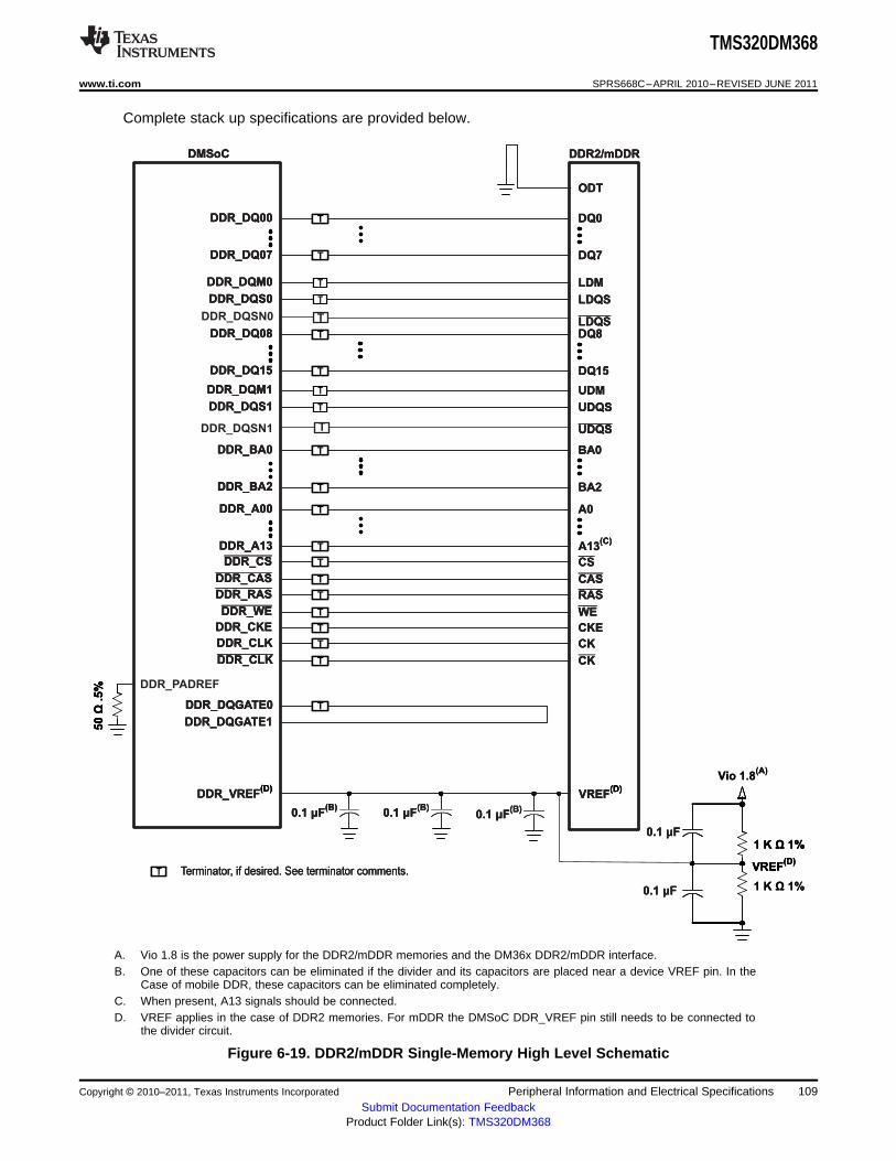
DMSoC
DDR_DQ00
DDR_DQ07
DDR2/mDDR
DDR_DQM0
DDR_DQS0
ODT
DQ0
DQ7
DDR_DQ08
DDR_DQ15
DQ8
DQ15
LDM
LDQS
LDQS
DDR_DQM1
DDR_DQS1
UDM
UDQS
UDQS
DDR_BA0
DDR_BA2
BA0
BA2
DDR_A00
DDR_A13
A0
A13(C)
DDR_CS
DDR_CAS
CS
CAS
DDR_RAS
DDR_WE
RAS
WE
DDR_CKE CKE
DDR_CLK
DDR_CLK
CK
CK
DDR_DQGATE0
DDR_DQGATE1
T
T
T
T
T
T
T
T
T
T
T
T
T
T
T
T
T
T
T
T
DDR_PADREF
VREF(D)
DDR_VREF(D)
0.1 μF(B)
0.1 μF(B)
0.1 μF(B)
50
.5Ω
%
T Terminator, if desired. See terminator comments.
DDR_DQSN0
DMSoC
DDR_DQ00
DDR_DQ07
DDR2/mDDR
DDR_DQM0
DDR_DQS0
ODT
DQ0
DQ7
DDR_DQ08
DDR_DQ15
DQ8
DQ15
LDM
LDQS
LDQS
DDR_DQM1
DDR_DQS1
UDM
UDQS
UDQS
DDR_BA0
DDR_BA2
BA0
BA2
DDR_A00
DDR_A13
A0
A13(C)
DDR_CS
DDR_CAS
CS
CAS
DDR_RAS
DDR_WE
RAS
WE
DDR_CKE CKE
DDR_CLK
DDR_CLK
CK
CK
DDR_DQGATE0
DDR_DQGATE1
T
T
T
T
T
T
T
T
T
T
T
T
T
T
T
T
T
T
T
T
VREF(D)
DDR_VREF(D)
0.1 μF(B)
0.1 μF(B)
0.1 μF(B)
50
.5Ω
%
T Terminator, if desired. See terminator comments.
DMSoC
DDR_DQ00
DDR_DQ07
DDR2/mDDR
DDR_DQM0
DDR_DQS0
ODT
DQ0
DQ7
DDR_DQ08
DDR_DQ15
DQ8
DQ15
LDM
LDQS
LDQS
DDR_DQM1
DDR_DQS1
UDM
UDQS
UDQS
DDR_BA0
DDR_BA2
BA0
BA2
DDR_A00
DDR_A13
A0
A13(C)
DDR_CS
DDR_CAS
CS
CAS
DDR_RAS
DDR_WE
RAS
WE
DDR_CKE CKE
DDR_CLK
DDR_CLK
CK
CK
DDR_DQGATE0
DDR_DQGATE1
T
T
T
T
T
T
T
T
T
T
T
T
T
T
T
T
T
T
T
T
VREF(D)
DDR_VREF(D)
1 K Ω 1%
Vio 1.8(A)
VREF(D)
1 K Ω 1%0.1 μF
0.1 μF1 K Ω 1%
Vio 1.8(A)
VREF(D)
1 K Ω 1%0.1 μF
0.1 μF1 K Ω 1%
VREF(D)
0.1 μF
0.1 μF
0.1 μF(B)
0.1 μF(B)
0.1 μF(B)
50
.5Ω
%
T Terminator, if desired. See terminator comments.
T
DDR_DQSN1 T
TMS320DM368
www.ti.com SPRS668C–APRIL 2010–REVISED JUNE 2011
Complete stack up specifications are provided below.
A. Vio 1.8 is the power supply for the DDR2/mDDR memories and the DM36x DDR2/mDDR interface.B. One of these capacitors can be eliminated if the divider and its capacitors are placed near a device VREF pin. In the
Case of mobile DDR, these capacitors can be eliminated completely.C. When present, A13 signals should be connected.D. VREF applies in the case of DDR2 memories. For mDDR the DMSoC DDR_VREF pin still needs to be connected to
the divider circuit.
Figure 6-19. DDR2/mDDR Single-Memory High Level Schematic
Copyright © 2010–2011, Texas Instruments Incorporated Peripheral Information and Electrical Specifications 109Submit Documentation Feedback
Product Folder Link(s): TMS320DM368
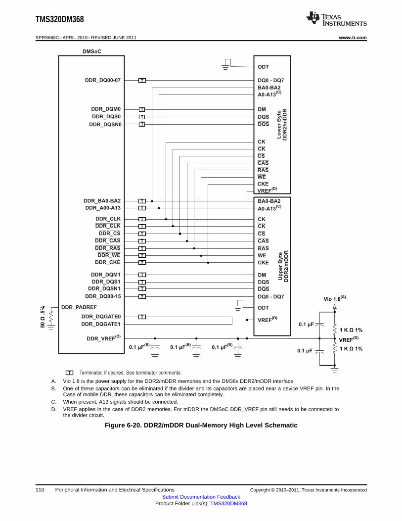
DMSoC
DDR_DQ00-07
Lo
wer
Byte
DD
R2/m
DD
RDDR_DQM0
DDR_DQS0
ODT
DQ0 - DQ7
BA0-BA2
CK
CK
DM
DQS
DQS
CS
CAS
RAS
DDR_BA0-BA2
CKE
BA0-BA2
DDR_A00-A13
DDR_CLK
A0-A13(C)
DDR_CLK
DDR_CS
CK
CS
DDR_CAS
DDR_RAS
CAS
RAS
DDR_WE WE
DDR_DQ08-15
DQS
DQ0 - DQ7
DDR_DQGATE0
DDR_DQGATE1
T
T
T
T
T
T
T
T
T
T
T
T
T
DDR_PADREF
VREF(D)
DDR_VREF(D)
1 K Ω 1%
Vio 1.8(A)
VREF(D)
1 K Ω 1%0.1 μF
0.1 μF
0.1 μF(B)
0.1 μF(B)
0.1 μF(B)
50
.5Ω
%
T Terminator, if desired. See terminator comments.
ODT
A0-A13(C)
WE
VREF(D)
Up
per
Byte
DD
R2/m
DD
R
CK
DDR_CKE CKET
DDR_DQM1 DMT
DDR_DQS1 DQST
DDR_DQSN0 T
DDR_DQSN1 T
TMS320DM368
SPRS668C–APRIL 2010–REVISED JUNE 2011 www.ti.com
A. Vio 1.8 is the power supply for the DDR2/mDDR memories and the DM36x DDR2/mDDR interface.B. One of these capacitors can be eliminated if the divider and its capacitors are placed near a device VREF pin. In the
Case of mobile DDR, these capacitors can be eliminated completely.C. When present, A13 signals should be connected.D. VREF applies in the case of DDR2 memories. For mDDR the DMSoC DDR_VREF pin still needs to be connected to
the divider circuit.
Figure 6-20. DDR2/mDDR Dual-Memory High Level Schematic
110 Peripheral Information and Electrical Specifications Copyright © 2010–2011, Texas Instruments Incorporated
Submit Documentation FeedbackProduct Folder Link(s): TMS320DM368

A1
A1
X
Y
OFFSET
Recommended DDR2/mDDR
Device Orientation
Y
Y
OFFSET
DDR2/mDDR
Device
DD
R2/m
DD
R
Co
ntr
oller
DMSoC
TMS320DM368
www.ti.com SPRS668C–APRIL 2010–REVISED JUNE 2011
Table 6-26. PCB Stack Up Specifications (1)
No. Parameter Min Typ Max Unit Notes
1 PCB Routing/Plane Layers 6
2 Signal Routing Layers 3
3 Full ground layers under DDR2/mDDR routing Region 2
4 Number of ground plane cuts allowed within DDR routing region 0
5 Number of ground reference planes required for each DDR2/mDDR 1routing layer
6 Number of layers between DDR2/mDDR routing layer and reference 0ground plane
7 PCB Routing Feature Size 4 Mils
8 PCB Trace Width w 4 Mils
9 DMSoC Device BGA pad size 0.3 mm
10 DDR2/mDDR Device BGA pad size See Note (2)
11 Single Ended Impedance, Zo 50 75 Ω12 Impedance Control Z-5 Z Z+5 Ω See Note (3)
(1) Consult the PCB fabricator to determine their preference for escape via size.(2) Please refer to the DDR2/mDDR device manufacturer documentation for the DDR2/mDDR device BGA pad size.(3) Z is the nominal singled ended impedance selected for the PCB specified by item 12.
6.10.3.1.4 Placement
Figure 6-21 shows the required placement for the device as well as the DDR2/mDDR devices. Thedimensions for Figure 6-21 are defined in Table 6-27. The placement does not restrict the side of the PCBthat the devices are mounted on. The ultimate purpose of the placement is to limit the maximum tracelengths and allow for proper routing space. For single-memory DDR2/mDDR systems, the secondDDR2/mDDR device is omitted from the placement.
Figure 6-21. DM368 and DDR2/mDDR Device Placement
Copyright © 2010–2011, Texas Instruments Incorporated Peripheral Information and Electrical Specifications 111Submit Documentation Feedback
Product Folder Link(s): TMS320DM368

A1
A1
DD
R2/m
DD
RC
on
tro
ller
DDR2/mDDRDevice
Region should encompass all DDR2/mDDR circuitry and variesdepending on placement. Non-DDR2/mDDR signals should not berouted on the DDR signal layers within the DDR2/mDDR keep outregion. Non-DDR2/mDDR signals may be routed in the regionprovided they are routed on layers separated from DDR2/mDDRsignal layers by a ground layer. No breaks should be allowed in thereference ground layers in this region. In addition, the 1.8 V powerplane should cover the entire keep out region.
TMS320DM368
SPRS668C–APRIL 2010–REVISED JUNE 2011 www.ti.com
Table 6-27. Placement Specifications
No. Parameter Min Max Unit Notes
1 X 1750 Mils See Notes (1), (2)
2 Y 1280 Mils See Notes (1), (2)
3 Y Offset 650 Mils See Notes (1). (2),(3)
4 DDR2/mDDR Keepout Region See Note (4)
5 Clearance from non-DDR2/mDDR signal to DDR2/mDDR Keepout Region 4 w See Note (5)
(1) See Figure 6-19 for dimension definitions.(2) Measurements from center of DMSoC device to center of DDR2/mDDR device.(3) For single memory systems it is recommended that Y Offset be as small as possible.(4) DDR2/mDDR Keepout region to encompass entire DDR2/mDDR routing area(5) Non-DDR2/mDDR signals allowed within DDR2/mDDR keepout region provided they are separated from DDR2/mDDR routing layers by
a ground plane.
6.10.3.1.5 DDR2/mDDR Keep Out Region
The region of the PCB used for the DDR2/mDDR circuitry must be isolated from other signals. TheDDR2/mDDR keep out region is defined for this purpose and is shown in Figure 6-22. The size of thisregion varies with the placement and DDR routing. Additional clearances required for the keep out regionare shown in Table 6-27.
Figure 6-22. DDR2/mDDR Keepout Region
112 Peripheral Information and Electrical Specifications Copyright © 2010–2011, Texas Instruments Incorporated
Submit Documentation FeedbackProduct Folder Link(s): TMS320DM368

TMS320DM368
www.ti.com SPRS668C–APRIL 2010–REVISED JUNE 2011
6.10.3.1.6 Bulk Bypass Capacitors
Bulk bypass capacitors are required for moderate speed bypassing of the DDR2/mDDR and othercircuitry. Table 6-28 contains the minimum numbers and capacitance required for the bulk bypasscapacitors. Note that this table only covers the bypass needs of the DMSoC and DDR2/mDDR interfaces.Additional bulk bypass capacitance may be needed for other circuitry.
Table 6-28. Bulk Bypass Capacitors
No. Parameter Min Max Unit Notes
1 VDD18_DDR Bulk Bypass Capacitor Count 3 Devices See Note(1)
2 VDD18_DDR Bulk Bypass Total Capacitance 30 uF
3 DDR#1 Bulk Bypass Capacitor Count 1 Devices See Note(1)
4 DDR#1 Bulk Bypass Total Capacitance 22 uF
5 DDR#2 Bulk Bypass Capacitor Count 1 Devices See Notes(1), (2)
6 DDR#2 Bulk Bypass Total Capacitance 22 uF See Note(2)
(1) These devices should be placed near the device they are bypassing, but preference should be given to the placement of the high-speed(HS) bypass caps.
(2) Only used on dual-memory systems
Copyright © 2010–2011, Texas Instruments Incorporated Peripheral Information and Electrical Specifications 113Submit Documentation Feedback
Product Folder Link(s): TMS320DM368

TMS320DM368
SPRS668C–APRIL 2010–REVISED JUNE 2011 www.ti.com
6.10.3.1.7 High-Speed Bypass Capacitors
High-speed (HS) bypass capacitors are critical for proper DDR2/mDDR interface operation. It isparticularly important to minimize the parasitic series inductance of the HS bypass cap,DMSoC/DDR2/mDDR power, and DMSoC/DDR2/mDDR ground connections. Table 6-29 contains thespecification for the HS bypass capacitors as well as for the power connections on the PCB.
6.10.3.1.8 Net Classes
Table 6-30 lists the clock net classes for the DDR2/mDDR interface. Table 6-31 lists the signal netclasses, and associated clock net classes, for the signals in the DDR2/mDDR interface. These net classesare used for the termination and routing rules that follow.
Table 6-29. High-Speed Bypass Capacitors
No. Parameter Min Max Unit Notes
1 HS Bypass Capacitor Package Size 0402 10 Mils See Note (1)
2 Distance from HS bypass capacitor to device being bypassed 250 Mils
3 Number of connection vias for each HS bypass capacitor 2 Vias See Note (2)
4 Trace length from bypass capacitor contact to connection via 1 30 Mils
5 Number of connection vias for each DDR2/mDDR device power or ground balls 1 Vias
6 Trace length from DDR2/mDDR device power ball to connection via 35 Mils
7 VDD18_DDR HS Bypass Capacitor Count 10 Devices See Note (3)
8 VDD18_DDR HS Bypass Capacitor Total Capacitance 1.2 uF
9 DDR#1 HS Bypass Capacitor Count 8 Devices See Note (3)
10 DDR#1 HS Bypass Capacitor Total Capacitance 0.4 uF
11 DDR#2 HS Bypass Capacitor Count 8 Devices See Notes(3), (4)
12 DDR#2 HS Bypass Capacitor Total Capacitance 0.4 uF See Note (4)
(1) LxW, 10 mil units, i.e., a 0402 is a 40x20 mil surface mount capacitor(2) An additional HS bypass capacitor can share the connection vias only if it is mounted on the opposite side of the board.(3) These devices should be placed as close as possible to the device being bypassed.(4) Only used on dual-memory systems
114 Peripheral Information and Electrical Specifications Copyright © 2010–2011, Texas Instruments Incorporated
Submit Documentation FeedbackProduct Folder Link(s): TMS320DM368
TMS320DM368
www.ti.com SPRS668C–APRIL 2010–REVISED JUNE 2011
Table 6-30. Clock Net Class Definitions
Clock Net Class DMSoC Pin Names
CK DDR_CLK/DDR_CLK
DQS0 DDR_DQS0/DDR_DQSN0
DQS1 DDR_DQS1/DDR_DQSN1
Table 6-31. Signal Net Class Definitions
Associated Clock NetClock Net Class Class DMSoC Pin Names
ADDR_CTRL CK DDR_BA[2:0], DDR_A[13:0], DDR_CS, DDR_CAS, DDR_RAS, DDR_WE,DDR_CKE
DQ0 DQS0 DDR_DQ[7:0], DDR_DQM0
DQ1 DQS1 DDR_DQ[15:8], DDR_DQM1
DQGATE CK, DQS0, DQS1 DDR_DQGATE0, DDR_DQGATE1
6.10.3.1.9 DDR2/mDDR Signal Termination
No terminations of any kind are required in order to meet signal integrity and overshoot requirements.Serial terminators are permitted, if desired, to reduce EMI risk; however, serial terminations are the onlytype permitted. Table 6-32 shows the specifications for the series terminators.
Table 6-32. DDR2/mDDR Signal Terminations
No. Parameter Min Typ Max Unit Notes
1 CK Net Class 0 10 Ω See Note (1)
2 ADDR_CTRL Net Class 0 22 Zo Ω See Notes (1),(2), (3)
3 Data Byte Net Classes (DQS0-DQS1, DQ0-DQ1) 0 22 Zo Ω See Notes (1),(2), (3), (4)
4 DQGATE Net Class (DQGATE) 0 10 Zo Ω See Notes (1),(2), (3)
(1) Only series termination is permitted, parallel or SST specifically disallowed.(2) Terminator values larger than typical only recommended to address EMI issues.(3) Termination value should be uniform across net class.(4) When no termination is used on data lines (0 Ωs), the DDR2/mDDR devices must be programmed to operate in 60% strength mode.
Copyright © 2010–2011, Texas Instruments Incorporated Peripheral Information and Electrical Specifications 115Submit Documentation Feedback
Product Folder Link(s): TMS320DM368
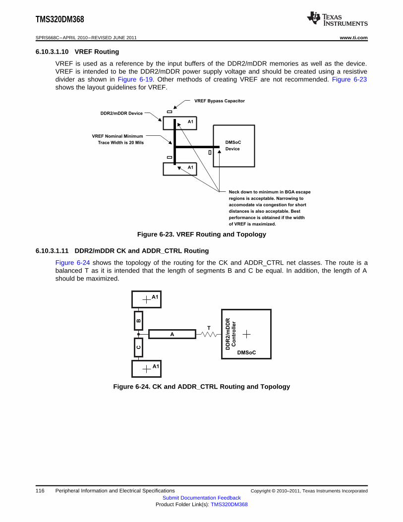
DMSoC
Device
A1
A1
DDR2/mDDR Device
VREF Nominal Minimum
Trace Width is 20 Mils
VREF Bypass Capacitor
Neck down to minimum in BGA escape
regions is acceptable. Narrowing to
accomodate via congestion for short
distances is also acceptable. Best
performance is obtained if the width
of VREF is maximized.
A1
A1
CB
A
T
DD
R2/m
DD
R
Co
ntr
oller
DMSoC
TMS320DM368
SPRS668C–APRIL 2010–REVISED JUNE 2011 www.ti.com
6.10.3.1.10 VREF Routing
VREF is used as a reference by the input buffers of the DDR2/mDDR memories as well as the device.VREF is intended to be the DDR2/mDDR power supply voltage and should be created using a resistivedivider as shown in Figure 6-19. Other methods of creating VREF are not recommended. Figure 6-23shows the layout guidelines for VREF.
Figure 6-23. VREF Routing and Topology
6.10.3.1.11 DDR2/mDDR CK and ADDR_CTRL Routing
Figure 6-24 shows the topology of the routing for the CK and ADDR_CTRL net classes. The route is abalanced T as it is intended that the length of segments B and C be equal. In addition, the length of Ashould be maximized.
Figure 6-24. CK and ADDR_CTRL Routing and Topology
116 Peripheral Information and Electrical Specifications Copyright © 2010–2011, Texas Instruments Incorporated
Submit Documentation FeedbackProduct Folder Link(s): TMS320DM368

A1
A1
E0T
E1T
E2
DMSoC
E3T
DD
R2/m
DD
R
Co
ntr
oller
T
TMS320DM368
www.ti.com SPRS668C–APRIL 2010–REVISED JUNE 2011
Table 6-33. CK and ADDR_CTRL Routing Specification (1)
No Parameter Min Typ Max Unit Notes
1 Center to center DQS-DQSN spacing 2w
2 CK A to B/A to C Skew Length Mismatch 25 Mils See Note (1)
3 CK B to C Skew Length Mismatch 25 Mils
4 Center to center CK to other DDR2/mDDR trace spacing 4w See Note (2)
5 CK/ADDR_CTRL nominal trace length CACLM-50 CACLM CACLM+50 Mils See Note (3)
6 ADDR_CTRL to CK Skew Length Mismatch 100 Mils
7 ADDR_CTRL to ADDR_CTRL Skew Length Mismatch 100 Mils
8 Center to center ADDR_CTRL to other DDR2/mDDR 4w See Note (2)
trace spacing
9 Center to center ADDR_CTRL to other ADDR_CTRL 3w See Note (2)
trace spacing
10 ADDR_CTRL A to B/A to C Skew Length Mismatch 100 Mils See Note (1)
11 ADDR_CTRL B to C Skew Length Mismatch 100 Mils
(1) Series terminator, if used, should be located closest to DMSoC.(2) Center to center spacing is allowed to fall to minimum (w) for up to 500 mils of routed length to accommodate BGA escape and routing
congestion.(3) CACLM is the longest Manhattan distance of the CK and ADDR_CTRL net classes.
Figure 6-25 shows the topology and routing for the DQS and DQ net classes; the routes are point to point.Skew matching across bytes is not needed nor recommended.
Figure 6-25. DQS and DQ Routing and Topology
Copyright © 2010–2011, Texas Instruments Incorporated Peripheral Information and Electrical Specifications 117Submit Documentation Feedback
Product Folder Link(s): TMS320DM368
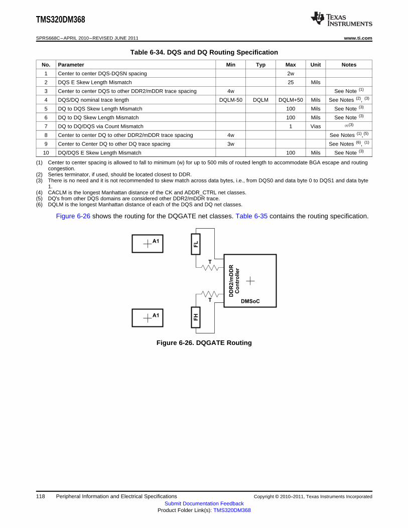
A1
A1
T
T
FL
FH
DD
R2/m
DD
R
Co
ntr
oller
DMSoC
TMS320DM368
SPRS668C–APRIL 2010–REVISED JUNE 2011 www.ti.com
Table 6-34. DQS and DQ Routing Specification
No. Parameter Min Typ Max Unit Notes
1 Center to center DQS-DQSN spacing 2w
2 DQS E Skew Length Mismatch 25 Mils
3 Center to center DQS to other DDR2/mDDR trace spacing 4w See Note (1)
4 DQS/DQ nominal trace length DQLM-50 DQLM DQLM+50 Mils See Notes (2), (3)
5 DQ to DQS Skew Length Mismatch 100 Mils See Note (3)
6 DQ to DQ Skew Length Mismatch 100 Mils See Note (3)
7 DQ to DQ/DQS via Count Mismatch 1 Vias (4) (3)
8 Center to center DQ to other DDR2/mDDR trace spacing 4w See Notes (1), (5)
9 Center to Center DQ to other DQ trace spacing 3w See Notes (6), (1)
10 DQ/DQS E Skew Length Mismatch 100 Mils See Note (3)
(1) Center to center spacing is allowed to fall to minimum (w) for up to 500 mils of routed length to accommodate BGA escape and routingcongestion.
(2) Series terminator, if used, should be located closest to DDR.(3) There is no need and it is not recommended to skew match across data bytes, i.e., from DQS0 and data byte 0 to DQS1 and data byte
1.(4) CACLM is the longest Manhattan distance of the CK and ADDR_CTRL net classes.(5) DQ's from other DQS domains are considered other DDR2/mDDR trace.(6) DQLM is the longest Manhattan distance of each of the DQS and DQ net classes.
Figure 6-26 shows the routing for the DQGATE net classes. Table 6-35 contains the routing specification.
Figure 6-26. DQGATE Routing
118 Peripheral Information and Electrical Specifications Copyright © 2010–2011, Texas Instruments Incorporated
Submit Documentation FeedbackProduct Folder Link(s): TMS320DM368

TMS320DM368
www.ti.com SPRS668C–APRIL 2010–REVISED JUNE 2011
Table 6-35. DQGATE Routing Specification
No. Parameter Min Typ Max Unit Notes
1 DQGATE Length F CKB0B1 See Note (1)
3 Center to center DQGATE to any other trace spacing 4w
4 DQS/DQ nominal trace length DQLM-50 DQLM DQLM+50 Mils
5 DQGATE Skew 100 Mils See Note (2)
(1) CKB0B1 is the sum of the length of the CK net plus the average length of the DQS0 and DQS1 nets.(2) Skew from CKB0B1
Copyright © 2010–2011, Texas Instruments Incorporated Peripheral Information and Electrical Specifications 119Submit Documentation Feedback
Product Folder Link(s): TMS320DM368
TMS320DM368
SPRS668C–APRIL 2010–REVISED JUNE 2011 www.ti.com
6.11 MMC/SD
The device includes MMC/SD Controllers which are compliant with MMC V3.31, Secure Digital Part 1Physical Layer Specification V1.1 and Secure Digital Input Output (SDIO) V2.0 specifications.
The device MMC/SD Controller has following features:• MultiMediaCard (MMC)• Secure Digital (SD) Memory Card• MMC/SD protocol support• SDIO protocol support• Programmable clock frequency• 512 bit Read/Write FIFO to lower system overhead• Slave EDMA transfer capability• SD High Capacity support
The device MMC/SD Controller does not support SPI mode.
6.11.1 MMC/SD Peripheral Register Description(s)
Table 6-36 lists the MMC/SD registers, their corresponding acronyms, and device memory locations(offsets).
Table 6-36. Multimedia Card/Secure Digital (MMC/SD) Card Controller Registers
OFFSET ACRONYM REGISTER DESCRIPTION
00h MMCCTL MMC Control Register
04h MMCCLK MMC Memory Clock Control Register
08h MMCST0 MMC Status Register 0
0Ch MMCST1 MMC Status Register 1
10h MMCIM MMC Interrupt Mask Register
14h MMCTOR MMC Response Time-Out Register
18h MMCTOD MMC Data Read Time-Out Register
1Ch MMCBLEN MMC Block Length Register
20h MMCNBLK MMC Number of Blocks Register
24h MMCNBLC MMC Number of Blocks Counter Register
28h MMCDRR MMC Data Receive Register
2Ch MMCDXR MMC Data Transmit Register
30h MMCCMD MMC Command Register
34h MMCARGHL MMC Argument Register
38h MMCRSP01 MMC Response Register 0 and 1
3Ch MMCRSP23 MMC Response Register 2 and 3
40h MMCRSP45 MMC Response Register 4 and 5
44h MMCRSP67 MMC Response Register 6 and 7
48h MMCDRSP MMC Data Response Register
50h MMCCIDX MMC Command Index Register
64h SDIOCTL SDIO Control Register
68h SDIOST0 SDIO Status Register 0
6Ch SDIOIEN SDIO Interrupt Enable Register
70h SDIOIST SDIO Interrupt Status Register
74h MMCFIFOCTL MMC FIFO Control Register
120 Peripheral Information and Electrical Specifications Copyright © 2010–2011, Texas Instruments Incorporated
Submit Documentation FeedbackProduct Folder Link(s): TMS320DM368

START XMIT Valid Valid Valid END
SD_CLK
SD_CMD
13
7
109
13 13 13
START XMIT Valid Valid Valid END
SD_CLK
SD_CMD
109
7
1
2
START D0 D1 Dx END
SD_CLK
SD_DATx
7
1414
10
9
14 14
TMS320DM368
www.ti.com SPRS668C–APRIL 2010–REVISED JUNE 2011
6.11.2 MMC/SD Electrical Data/Timing
Table 6-37. Timing Requirements for MMC/SD Module(see Figure 6-28 and Figure 6-30)
DEVICE
NO. FAST MODE STANDARD MODE UNIT
MIN MAX MIN MAX
1 tsu(CMDV-CLKH) Setup time, SD_CMD valid before SD_CLK high 2.7 2.7 ns
2 th(CLKH-CMDV) Hold time, SD_CMD valid after SD_CLK high 2.5 2.5 ns
3 tsu(DATV-CLKH) Setup time, SD_DATx valid before SD_CLK high 2.7 2.7 ns
4 th(CLKH-DATV) Hold time, SD_DATx valid after SD_CLK high 2.5 2.5 ns
Table 6-38. Switching Characteristics Over Recommended Operating Conditions for MMC/SD Module(see Figure 6-27 through Figure 6-30)
DEVICE
STANDARDNO. PARAMETER FAST MODE UNITMODE
MIN MAX MIN MAX
7 f(CLK) Operating frequency, SD_CLK 0 50 0 25 MHz
8 f(CLK_ID) Identification mode frequency, SD_CLK 0 400 0 400 KHz
9 tW(CLKL) Pulse width, SD_CLK low 6.5 6.5 ns
10 tW(CLKH) Pulse width, SD_CLK high 6.5 6.5 ns
11 tr(CLK) Rise time, SD_CLK 3 3 ns
12 tf(CLK) Fall time, SD_CLK 3 3 ns
13 td(CLKL-CMD) Delay time, SD_CLK low to SD_CMD transition -4.1 1.5 -4.1 1.5 ns
14 td(CLKL-DAT) Delay time, SD_CLK low to SD_DATx transition -4.1 1.5 -4.1 1.5 ns
Figure 6-27. MMC/SD Host Command Timing
Figure 6-28. MMC/SD Card Response Timing
Figure 6-29. MMC/SD Host Write Timing
Copyright © 2010–2011, Texas Instruments Incorporated Peripheral Information and Electrical Specifications 121Submit Documentation Feedback
Product Folder Link(s): TMS320DM368

Start D0 D1 Dx End
7
SD_CLK
SD_DATx
910
4
3 3
4
TMS320DM368
SPRS668C–APRIL 2010–REVISED JUNE 2011 www.ti.com
Figure 6-30. MMC/SD Host Read and Card CRC Status Timing
122 Peripheral Information and Electrical Specifications Copyright © 2010–2011, Texas Instruments Incorporated
Submit Documentation FeedbackProduct Folder Link(s): TMS320DM368
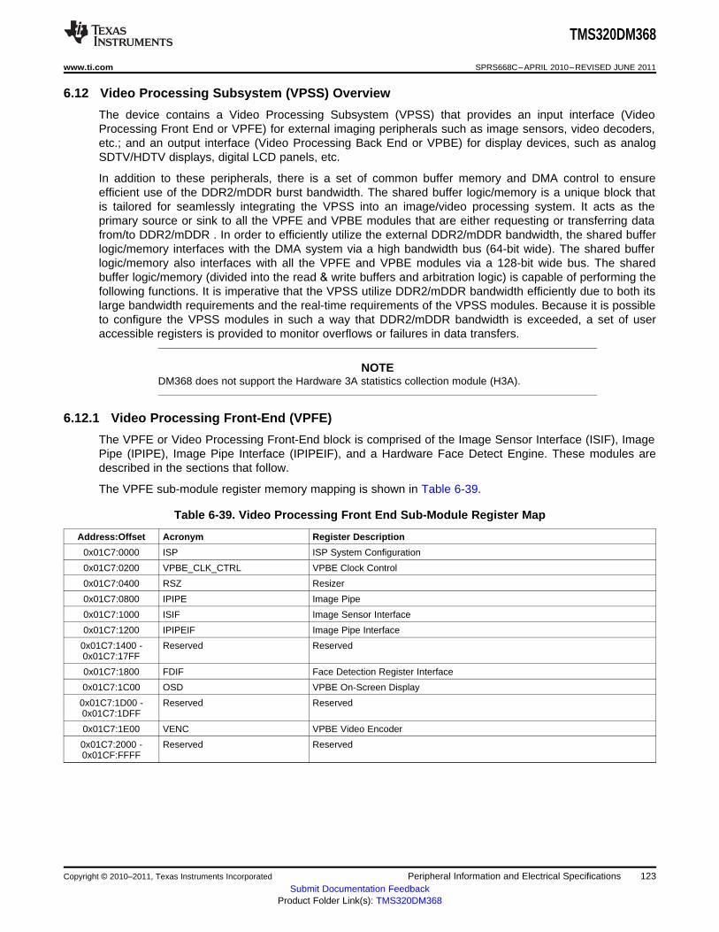
TMS320DM368
www.ti.com SPRS668C–APRIL 2010–REVISED JUNE 2011
6.12 Video Processing Subsystem (VPSS) Overview
The device contains a Video Processing Subsystem (VPSS) that provides an input interface (VideoProcessing Front End or VPFE) for external imaging peripherals such as image sensors, video decoders,etc.; and an output interface (Video Processing Back End or VPBE) for display devices, such as analogSDTV/HDTV displays, digital LCD panels, etc.
In addition to these peripherals, there is a set of common buffer memory and DMA control to ensureefficient use of the DDR2/mDDR burst bandwidth. The shared buffer logic/memory is a unique block thatis tailored for seamlessly integrating the VPSS into an image/video processing system. It acts as theprimary source or sink to all the VPFE and VPBE modules that are either requesting or transferring datafrom/to DDR2/mDDR . In order to efficiently utilize the external DDR2/mDDR bandwidth, the shared bufferlogic/memory interfaces with the DMA system via a high bandwidth bus (64-bit wide). The shared bufferlogic/memory also interfaces with all the VPFE and VPBE modules via a 128-bit wide bus. The sharedbuffer logic/memory (divided into the read & write buffers and arbitration logic) is capable of performing thefollowing functions. It is imperative that the VPSS utilize DDR2/mDDR bandwidth efficiently due to both itslarge bandwidth requirements and the real-time requirements of the VPSS modules. Because it is possibleto configure the VPSS modules in such a way that DDR2/mDDR bandwidth is exceeded, a set of useraccessible registers is provided to monitor overflows or failures in data transfers.
NOTEDM368 does not support the Hardware 3A statistics collection module (H3A).
6.12.1 Video Processing Front-End (VPFE)
The VPFE or Video Processing Front-End block is comprised of the Image Sensor Interface (ISIF), ImagePipe (IPIPE), Image Pipe Interface (IPIPEIF), and a Hardware Face Detect Engine. These modules aredescribed in the sections that follow.
The VPFE sub-module register memory mapping is shown in Table 6-39.
Table 6-39. Video Processing Front End Sub-Module Register Map
Address:Offset Acronym Register Description
0x01C7:0000 ISP ISP System Configuration
0x01C7:0200 VPBE_CLK_CTRL VPBE Clock Control
0x01C7:0400 RSZ Resizer
0x01C7:0800 IPIPE Image Pipe
0x01C7:1000 ISIF Image Sensor Interface
0x01C7:1200 IPIPEIF Image Pipe Interface
0x01C7:1400 - Reserved Reserved0x01C7:17FF
0x01C7:1800 FDIF Face Detection Register Interface
0x01C7:1C00 OSD VPBE On-Screen Display
0x01C7:1D00 - Reserved Reserved0x01C7:1DFF
0x01C7:1E00 VENC VPBE Video Encoder
0x01C7:2000 - Reserved Reserved0x01CF:FFFF
Copyright © 2010–2011, Texas Instruments Incorporated Peripheral Information and Electrical Specifications 123Submit Documentation Feedback
Product Folder Link(s): TMS320DM368

TMS320DM368
SPRS668C–APRIL 2010–REVISED JUNE 2011 www.ti.com
6.12.1.1 Image Sensor Interface (ISIF)
The ISIF is responsible for accepting raw (unprocessed) image/video data from a sensor (CMOS or CCD).In addition, the ISIF can accept YUV video data in numerous formats, typically from so-called videodecoder devices. In case of raw inputs, the ISIF output requires additional image processing to transformthe raw input image to the final processed image. This processing can be done either on-the-fly in IPIPEor in software on the ARM and MPEG/JPEG and HD Video Image coprocessor subsystems. The ISIF isprogrammed via control and parameter registers. The following features are supported by the ISIFmodule.• Support for conventional Bayer pattern, pixel summation mode, and RGB stripe sensor formats.• Support for the various pixel summation mode formats is provided via a data reformatter of ISIF, which
transforms any specific sensor formats to the Bayer format. The maximum line width supported by thereformatter is 4736 pixels.
• Image processing steps applicable to RGB stripe sensors are limited to color-dependent gain controland black level offset control."
• Generates HD/VD timing signals and field ID to an external timing generator, or can synchronize to theexternal timing generator.
• Support for progressive and interlaced sensors (hardware support for up to 2 fields and firmwaresupport for higher number of fields, typically 3-, 4-, and 5-field sensors.
• Support for up to 32K pixels (image size) in both the horizontal and vertical direction.• Support for up to 120 MHz sensor clock.• Support for ITU-R BT.656/1120 standard format.• Support for YCbCr 422 format, either 8- or 16-bit with discrete HSYNC and VSYNC signals.• Support for up to 16-bit input.• Support for color space conversion.• Digital clamp with Horizontal/Vertical offset drift compensation.• Vertical Line defect correction based on a lookup table that contains defect position.• Support for color-dependent gain control and black level offset control.• Ability to control output to the DDR2/mDDR via an external write enable signal.• Support for down sampling via programmable culling patterns.• Support for 12-bit to 8-bit DPCM compression.• Support for 10-bit to 8-bit A-law compression.• Support for generating output to range 16-bits, 12-bits, and 8-bits wide (8-bits wide allows for 50%
saving in storage area).• OTF DPC• Noise Filter• 2D edge enhancement
The ISIF register memory mapping (offsets) is shown in Table 6-40.
Table 6-40. Image Sensor Interface (ISIF) Registers
Offset Acronym Register Description
0h SYNCEN Synchronization Enable
4h MODESET Mode Setup
8h HDW HD pulse width
Ch VDW VD pulse width
10h PPLN Pixels per line
14h LPFR Lines per frame
18h SPH Start pixel horizontal
1Ch LNH Number of pixels in line
124 Peripheral Information and Electrical Specifications Copyright © 2010–2011, Texas Instruments Incorporated
Submit Documentation FeedbackProduct Folder Link(s): TMS320DM368
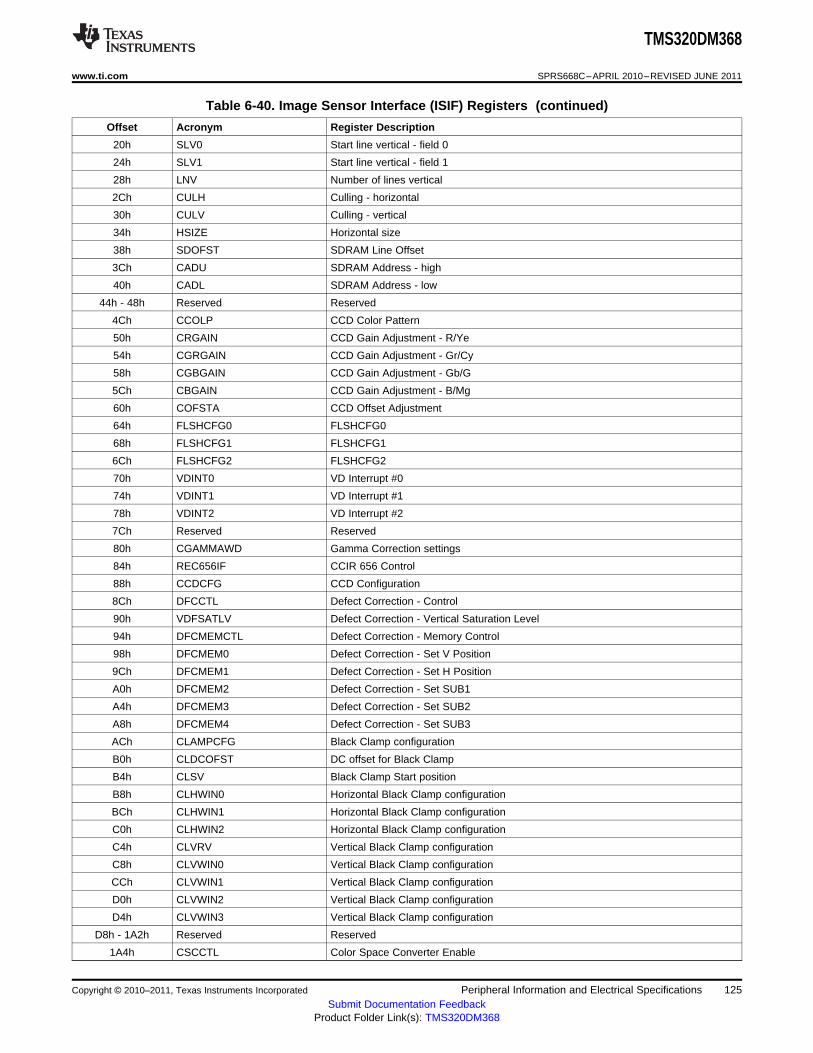
TMS320DM368
www.ti.com SPRS668C–APRIL 2010–REVISED JUNE 2011
Table 6-40. Image Sensor Interface (ISIF) Registers (continued)
Offset Acronym Register Description
20h SLV0 Start line vertical - field 0
24h SLV1 Start line vertical - field 1
28h LNV Number of lines vertical
2Ch CULH Culling - horizontal
30h CULV Culling - vertical
34h HSIZE Horizontal size
38h SDOFST SDRAM Line Offset
3Ch CADU SDRAM Address - high
40h CADL SDRAM Address - low
44h - 48h Reserved Reserved
4Ch CCOLP CCD Color Pattern
50h CRGAIN CCD Gain Adjustment - R/Ye
54h CGRGAIN CCD Gain Adjustment - Gr/Cy
58h CGBGAIN CCD Gain Adjustment - Gb/G
5Ch CBGAIN CCD Gain Adjustment - B/Mg
60h COFSTA CCD Offset Adjustment
64h FLSHCFG0 FLSHCFG0
68h FLSHCFG1 FLSHCFG1
6Ch FLSHCFG2 FLSHCFG2
70h VDINT0 VD Interrupt #0
74h VDINT1 VD Interrupt #1
78h VDINT2 VD Interrupt #2
7Ch Reserved Reserved
80h CGAMMAWD Gamma Correction settings
84h REC656IF CCIR 656 Control
88h CCDCFG CCD Configuration
8Ch DFCCTL Defect Correction - Control
90h VDFSATLV Defect Correction - Vertical Saturation Level
94h DFCMEMCTL Defect Correction - Memory Control
98h DFCMEM0 Defect Correction - Set V Position
9Ch DFCMEM1 Defect Correction - Set H Position
A0h DFCMEM2 Defect Correction - Set SUB1
A4h DFCMEM3 Defect Correction - Set SUB2
A8h DFCMEM4 Defect Correction - Set SUB3
ACh CLAMPCFG Black Clamp configuration
B0h CLDCOFST DC offset for Black Clamp
B4h CLSV Black Clamp Start position
B8h CLHWIN0 Horizontal Black Clamp configuration
BCh CLHWIN1 Horizontal Black Clamp configuration
C0h CLHWIN2 Horizontal Black Clamp configuration
C4h CLVRV Vertical Black Clamp configuration
C8h CLVWIN0 Vertical Black Clamp configuration
CCh CLVWIN1 Vertical Black Clamp configuration
D0h CLVWIN2 Vertical Black Clamp configuration
D4h CLVWIN3 Vertical Black Clamp configuration
D8h - 1A2h Reserved Reserved
1A4h CSCCTL Color Space Converter Enable
Copyright © 2010–2011, Texas Instruments Incorporated Peripheral Information and Electrical Specifications 125Submit Documentation Feedback
Product Folder Link(s): TMS320DM368

TMS320DM368
SPRS668C–APRIL 2010–REVISED JUNE 2011 www.ti.com
Table 6-40. Image Sensor Interface (ISIF) Registers (continued)
Offset Acronym Register Description
1A8h CSCM0 Color Space Converter - Coefficients #0
1ACh CSCM1 Color Space Converter - Coefficients #1
1B0h CSCM2 Color Space Converter - Coefficients #2
1B4h CSCM3 Color Space Converter - Coefficients #3
1B8h CSCM4 Color Space Converter - Coefficients #4
1BCh CSCM5 Color Space Converter - Coefficients #5
1C0h CSCM6 Color Space Converter - Coefficients #6
1C4h CSCM7 Color Space Converter - Coefficients #7
6.12.1.2 The Image Pipe Interface (IPIPEIF)
The IPIPEIF is data and sync signals interface module for ISIF and IPIPE. Data source of this module issensor parallel port, ISIF or SDRAM and the selected data is output to ISIF and IPIPE. This module alsooutputs black frame subtraction (two-way) data which is generated by subtracting SDRAM data fromsensor parallel port or ISIF data and vice versa. Depending on the functions performed, it may alsoreadjust the HD, VD, and PCLK timing to the IPIPE and/or ISIF input.
The IPIPEIF module supports the following features:• Up to 16-bit sensor data input• Dark-frame subtract of raw image stored in SDRAM from image coming from sensor parallel port or
ISIF• 8-10, 8-12 DPCM decompression of 10-8, 12-8 compressed data in SDRAM• Inverse ALAW decompression of RAW data from SDRAM• (1,2,1) average filtering before horizontal decimation• Horizontal decimation (downsizing) of input lines to <= 2160 maximum required by the IPIPE• Gain multiply for output data to IPIPE• Simple defect correction to prevent a subtraction of defect pixel• 8-bit, 12-bit unpacking of 8-bit, 12-bit packed SDRAM data
The IPIPE register memory mapping (offsets) is shown in Table 6-41.
Table 6-41. Image Pipe Input Interface (IPIPEIF) Registers
Address Acronym Register Description
0h ENABLE IPIPE I/F Enable
4h CFG1 IPIPE I/F Configuration
8h PPLN IPIPE I/F Interval of HD / Start pixel in HD
Ch LPFR IPIPE I/F Interval of VD / Start line in VD
10h HNUM IPIPE I/F Number of valid pixels per line
14h VNUM IPIPE I/F Number of valid lines per frame
18h ADDRU IPIPE I/F Memory Address (Upper)
1Ch ADDRL IPIPE I/F Memory Address (Lower)
20h ADOFS IPIPE I/F Address offset of each line
24h RSZ IPIPE I/F Horizontal Resizing Parameter
28h GAIN IPIPE I/F Gain Parameter
2Ch DPCM IPIPE I/F DPCM Configuration
30h CFG2 IPIPE I/F Configuration 2
34h INIRSZ IPIPE I/F Initial position of resize
38h OCLIP IPIPE I/F Output clipping value
3Ch DTUDF IPIPE I/F Data underflow error status
126 Peripheral Information and Electrical Specifications Copyright © 2010–2011, Texas Instruments Incorporated
Submit Documentation FeedbackProduct Folder Link(s): TMS320DM368

TMS320DM368
www.ti.com SPRS668C–APRIL 2010–REVISED JUNE 2011
Table 6-41. Image Pipe Input Interface (IPIPEIF) Registers (continued)
Address Acronym Register Description
40h CLKDIV IPIPE I/F Clock rate configuration
44h DPC1 IPIPE I/F Defect pixel correction
48h DPC2 IPIPE I/F Defect pixel correction
6.12.1.3 Image Pipe – Hardware Image Signal Processor (IPIPE)
The Image Pipe (IPIPE) is a programmable hardware image processing module that generates imagedata in YCbCr-4:2:2 or YCbCr-4:2:0 formats from raw CCD/CMOS data. An image resizer is also fullyintegrated within this module. The IPIPE can also be configured to operate in a resize-only mode, whichallows YCbCr-4:2:2 or YCbCr-4:2:0 to be resized without processing every module in the IPIPE.
The following features are supported by the IPIPE:• 12-bit RAW data image processing or 16-bit YCbCr resizing• RGB Bayer pattern for input color filter array; does not support complementary color pattern, stripe
pattern, or Foveon™ sensors.• Requires at least eight pixels for horizontal blanking and four lines for vertical blanking. In one shot
mode, 16 blanking lines after processing area are required.• Maximum horizontal and vertical offset of IPIPE processing area from synchronous signal is 65534• Maximum input and output widths up to 2176 pixels wide (1088 for RSZ[2]).• Raw pass-through mode for images wider than 2176 pixels (up to 8190 pixels)• Automatic mirroring of pixels/lines when edge processing is performed so that the width and height is
consistent throughout.• Defect pixel correction using
– Lookup table method that contains row and column position of the pixel to be corrected– On-the-fly adaptive method
• Offset and gain control for white balancing at each color component (WB).• CFA interpolation for good quality CFA interpolation• Programmable RGB to RGB blending matrix (9 coefficients for the 3x3 matrix). (RGB2RGB module)• Separate lookup tables for gamma correction on each of R, G and B components for display through
piece-wise linear interpolation approach• 4:4:4 data to 4:2:2 data conversion by chroma low-pass filtering and down sampling to Cb and Cr.
(4:4:4 to 4:2:2 module)• Programmable look-up table for luminance edge enhancement. Adjustable brightness and contrast for
Y component (Edge Enhancer module)• Programmable down or up-sampling filter for both horizontal and vertical directions with range from
1/16x to 16x, in which the filter outputs two images with different magnification simultaneously (Resizermodule)
• 4:2:2 to 4:2:0 conversion that can be done in the resizing block• Different data formats [YCbCr (4:2:2 or 4:2:0), RGB (32bit/16bit), Raw data] are available while storing
data in the SDRAM from IPIPE• Flipping image horizontally and/or vertically• Programmable histogram engine (4 windows, 256 bins)• Boxcar calculation (1/8 or 1/16 size).
The IPIPE register memory mapping (offsets) is shown in Table 6-42.
Copyright © 2010–2011, Texas Instruments Incorporated Peripheral Information and Electrical Specifications 127Submit Documentation Feedback
Product Folder Link(s): TMS320DM368

TMS320DM368
SPRS668C–APRIL 2010–REVISED JUNE 2011 www.ti.com
Table 6-42. IPIPE Registers
Offset Acronym Register Description
0h SRC_EN IPIPE Enable
04h SRC_MODE One Shot Mode
08h SRC_FMT Input/Output Data Paths
Ch SRC_COL Color Pattern
10h SRC_VPS Vertical Start Position
14h SRC_VSZ Vertical Processing Size
18h SRC_HPS Horizontal Start Position
1Ch SRC_HSZ Horizontal Processing Size
24h DMA_STA Status Flags (Reserved)
48h GCK_MMR MMR Gated Clock Control
2Ch GCK_PIX PCLK Gated Clock Control
30h Reserved Reserved
34h DPC_LUT_EN LUTDPC (=LUT Defect Pixel Correction): Enable
38h DPC_LUT_SEL LUTDPC: Processing Mode Selection
3Ch DPC_LUT_ADR LUTDPC: Start Address in LUT
40h DPC_LUT_SIZ LUTDPC: Number of available entries in LUT
1D0h WB2_OFT_R WB2 (=White Balance): Offset
1D4h WB2_OFT_GR WB2: Offset
1D8h WB2_OFT_GB WB2: Offset
1DCh WB2_OFT_B WB2: Offset
1E0h WB2_WGN_R WB2: Gain
1E4h WB2_WGN_GR WB2: Gain
1E8h WB2_WGN_GB WB2: Gain
1ECh WB2_WGN_B WB2: Gain
1F0h-228h Reserved Reserved
22Ch RGB1_MUL_RR RGB1 (=1st RGB2RGB conv): Matrix Coefficient
230h RGB1_MUL_GR RGB1: Matrix Coefficient
234h RGB1_MUL_BR RGB1: Matrix Coefficient
238h RGB1_MUL_RG RGB1: Matrix Coefficient
23Ch RGB1_MUL_GG RGB1: Matrix Coefficient
240h RGB1_MUL_BG RGB1: Matrix Coefficient
244h RGB1_MUL_RB RGB1: Matrix Coefficient
248h RGB1_MUL_GB RGB1: Matrix Coefficient
24Ch RGB1_MUL_BB RGB1: Matrix Coefficient
250h RGB1_OFT_OR RGB1: Offset
254h RGB1_OFT_OG RGB1: Offset
258h RGB1_OFT_OB RGB1: Offset
25Ch GMM_CFG Gamma Correction Configuration
294h YUV_ADJ YUV (RGB2YCbCr conv): Luminance Adjustment (contrast & brightness)
298h YUV_MUL_RY YUV: Matrix Coefficient
29Ch YUV_MUL_GY YUV: Matrix Coefficient
2A0h YUV_MUL_BY YUV: Matrix Coefficient
2A4h YUV_MUL_RCB YUV: Matrix Coefficient
2A8h YUV_MUL_GCB YUV: Matrix Coefficient
2ACh YUV_MUL_BCB YUV: Matrix Coefficient
2B0h YUV_MUL_RCR YUV: Matrix Coefficient
2B4h YUV_MUL_GCR YUV: Matrix Coefficient
128 Peripheral Information and Electrical Specifications Copyright © 2010–2011, Texas Instruments Incorporated
Submit Documentation FeedbackProduct Folder Link(s): TMS320DM368

TMS320DM368
www.ti.com SPRS668C–APRIL 2010–REVISED JUNE 2011
Table 6-42. IPIPE Registers (continued)
Offset Acronym Register Description
2B8h YUV_MUL_BCR YUV: Matrix Coefficient
2BCh YUV_OFT_Y YUV: Offset
2C0h YUV_OFT_CB YUV: Offset
2C4h YUV_OFT_CR YUV: Offset
2C8h YUV_PHS Chrominance Position (for 422 down sampler)
2D4h YEE_EN YEE (=Edge Enhancer): Enable
2D8h YEE_TYP YEE: Method Selection
2DCh YEE_SHF YEE: HPF Shift Length
2E0h YEE_MUL_00 YEE: HPF Coefficient
2E4h YEE_MUL_01 YEE: HPF Coefficient
2E8h YEE_MUL_02 YEE: HPF Coefficient
2ECh YEE_MUL_10 YEE: HPF Coefficient
2F0h YEE_MUL_11 YEE: HPF Coefficient
2F4h YEE_MUL_12 YEE: HPF Coefficient
2F8h YEE_MUL_20 YEE: HPF Coefficient
2FCh YEE_MUL_21 YEE: HPF Coefficient
300h YEE_MUL_22 YEE: HPF Coefficient
304h YEE_THR YEE: Lower Threshold before referring to LUT
308h YEE_E_GAN YEE: Edge Sharpener Gain
30Ch YEE_E_THR_1 YEE: Edge Sharpener HP Value Lower Threshold
310h YEE_E_THR_2 YEE: Edge Sharpener HP Value Upper Limit
314h YEE_G_GAN YEE: Edge Sharpener Gain on Gradient
318h YEE_G_OFT YEE: Edge Sharpener Offset on Gradient
380h BOX_EN BOX (=Boxcar) Enable
384h BOX_MODE BOX: One Shot Mode
388h BOX_TYP BOX: Block Size (16x16 or 8x8)
38Ch BOX_SHF BOX: Down shift value of input
390h BOX_SDR_SAD_H BOX: SDRAM Address MSB
394h BOX_SDR_SAD_L BOX: SDRAM Address LSB
398h Reserved Reserved
39Ch HST_EN HST (=Histogram): Enable
3A0h HST_MODE HST: One Shot Mode
3A4h HST_SEL HST: Source Select
3A8h HST_PARA HST: Parameters Select
3ACh HST_0_VPS HST: Vertical Start Position
3B0h HST_0_VSZ HST: Vertical Size
3B4h HST_0_HPS HST: Horizontal Start Position
3B8h HST_0_HSZ HST: Horizontal Size
3BCh HST_1_VPS HST: Vertical Start Position
3C0h HST_1_VSZ HST: Vertical Size
3C4h HST_1_HPS HST: Horizontal Start Position
3C8h HST_1_HSZ HST: Horizontal Size
3CCh HST_2_VPS HST: Vertical Start Position
3D0h HST_2_VSZ HST: Vertical Size
3D4h HST_2_HPS HST: Horizontal Start Position
3D8h HST_2_HSZ HST: Horizontal Size
3DCh HST_3_VPS HST: Vertical Start Position
Copyright © 2010–2011, Texas Instruments Incorporated Peripheral Information and Electrical Specifications 129Submit Documentation Feedback
Product Folder Link(s): TMS320DM368

TMS320DM368
SPRS668C–APRIL 2010–REVISED JUNE 2011 www.ti.com
Table 6-42. IPIPE Registers (continued)
Offset Acronym Register Description
3E0h HST_3_VSZ HST: Vertical Size
3E4h HST_3_HPS HST: Horizontal Start Position
3E8h HST_3_HSZ HST: Horizontal Size
3ECh HST_TBL HST: Table Select
3F0h HST_MUL_R HST: Matrix Coefficient
3F4h HST_MUL_GR HST: Matrix Coefficient
3F8h HST_MUL_GB HST: Matrix Coefficient
3FCh HST_MUL_B HST: Matrix Coefficient
6.12.1.4 Face Detection Module
The following features are supported on the Face Detection module:• High detection rate of close to 100% under most conditions• Allows detection in different directions - up, left, and right• Allows detection with rotation in plane (RIP) - ±45°, @ 0°/+90°/-90°• Allows detection for rotation out of plane (ROP)
– Horizontal (left/right) pan: ±60°– Vertical (up/down) tilt: ±30°
• Configurable minimum face size of 20 - 40 pixels• Configurable region of interest in the input frame• Configurable start position in the input frame• Supports up to 35 face detections in a single frame• Interrupt generation to ARM using the Video Processing Subsystem (VPSS) multiplexed interrupt
mechanism• Robust performance in low light conditions, night vision, monochromatic, and false color sensing as
skin tone not used for face detection• Supported input size is (256X192)• Input format is 8-bit gray scale data
The Face Detection Module register memory mapping (offsets) is shown in Table 6-43.
Table 6-43. Face Detection Module Registers
Offset Acronym Register Description
0x000 FDIF_PID FDIF PID
0x008 FDIF_INTEN FDIF Interrupt enable
0x00C FDIF_PICADDR FDIF Picture Data address
0x010 FDIF_WKADDR FDIF Work Area address
0x020 FD_CTRL FD Core Control Register
0x024 FD_DNUM Detect number
0x028 FD_DCOND Detect Condition set register
0x02C FD_STARTX X Start address
0x030 FD_STARTY Y Start address
0x034 FD_SIZEX X Size for detection
0x038 FD_SIZEY Y Size for detection
0x03C FD_LHIT Detect process threshold
0x100 FD_CENTERX1 Detect Result Center X Address
0x104 FD_CENTERY1 Detect Result Center Y Address
0x108 FD_CONFSIZE1 Detect Result Confidence/Size
130 Peripheral Information and Electrical Specifications Copyright © 2010–2011, Texas Instruments Incorporated
Submit Documentation FeedbackProduct Folder Link(s): TMS320DM368

TMS320DM368
www.ti.com SPRS668C–APRIL 2010–REVISED JUNE 2011
Table 6-43. Face Detection Module Registers (continued)
Offset Acronym Register Description
0x10C FD_ANGLE1 Detect Angle
0x110 FD_CENTERX2 Detect Result Center X Address
0x114 FD_CENTERY2 Detect Result Center Y Address
0x118 FD_CONFSIZE2 Detect Result Confidence/Size
0x11C FD_ANGLE2 Detect Angle
0x120 FD_CENTERX3 Detect Result Center X Address
0x124 FD_CENTERY3 Detect Result Center Y Address
0x128 FD_CONFSIZE3 Detect Result Confidence/Size
0x12C FD_ANGLE3 Detect Angle
0x130 FD_CENTERX4 Detect Result Center X Address
0x134 FD_CENTERY4 Detect Result Center Y Address
0x138 FD_CONFSIZE4 Detect Result Confidence/Size
0x13C FD_ANGLE4 Detect Angle
0x140 FD_CENTERX5 Detect Result Center X Address
0x144 FD_CENTERY5 Detect Result Center Y Address
0x148 FD_CONFSIZE5 Detect Result Confidence/Size
0x14C FD_ANGLE5 Detect Angle
0x150 FD_CENTERX6 Detect Result Center X Address
0x154 FD_CENTERY6 Detect Result Center Y Address
0x158 FD_CONFSIZE6 Detect Result Confidence/Size
0x15C FD_ANGLE6 Detect Angle
0x160 FD_CENTERX7 Detect Result Center X Address
0x164 FD_CENTERY7 Detect Result Center Y Address
0x168 FD_CONFSIZE7 Detect Result Confidence/Size
0x16C FD_ANGLE7 Detect Angle
0x170 FD_CENTERX8 Detect Result Center X Address
0x174 FD_CENTERY8 Detect Result Center Y Address
0x178 FD_CONFSIZE8 Detect Result Confidence/Size
0x17C FD_ANGLE8 Detect Angle
0x180 FD_CENTERX9 Detect Result Center X Address
0x184 FD_CENTERY9 Detect Result Center Y Address
0x188 FD_CONFSIZE9 Detect Result Confidence/Size
0x18C FD_ANGLE9 Detect Angle
0x190 FD_CENTERX10 Detect Result Center X Address
0x194 FD_CENTERY10 Detect Result Center Y Address
0x198 FD_CONFSIZE10 Detect Result Confidence/Size
0x19C FD_ANGLE10 Detect Angle
0x1A0 FD_CENTERX11 Detect Result Center X Address
0x1A4 FD_CENTERY11 Detect Result Center Y Address
0x1A8 FD_CONFSIZE11 Detect Result Confidence/Size
0x1AC FD_ANGLE11 Detect Angle
0x1B0 FD_CENTERX12 Detect Result Center X Address
0x1B4 FD_CENTERY12 Detect Result Center Y Address
0x1B8 FD_CONFSIZE12 Detect Result Confidence/Size
0x1BC FD_ANGLE12 Detect Angle
0x1C0 FD_CENTERX13 Detect Result Center X Address
0x1C4 FD_CENTERY13 Detect Result Center Y Address
Copyright © 2010–2011, Texas Instruments Incorporated Peripheral Information and Electrical Specifications 131Submit Documentation Feedback
Product Folder Link(s): TMS320DM368

TMS320DM368
SPRS668C–APRIL 2010–REVISED JUNE 2011 www.ti.com
Table 6-43. Face Detection Module Registers (continued)
Offset Acronym Register Description
0x1C8 FD_CONFSIZE13 Detect Result Confidence/Size
0x1CC FD_ANGLE13 Detect Angle
0x1D0 FD_CENTERX14 Detect Result Center X Address
0x1D4 FD_CENTERY14 Detect Result Center Y Address
0x1D8 FD_CONFSIZE14 Detect Result Confidence/Size
0x1DC FD_ANGLE14 Detect Angle
0x1E0 FD_CENTERX15 Detect Result Center X Address
0x1E4 FD_CENTERY15 Detect Result Center Y Address
0x1E8 FD_CONFSIZE15 Detect Result Confidence/Size
0x1EC FD_ANGLE15 Detect Angle
0x1F0 FD_CENTERX16 Detect Result Center X Address
0x1F4 FD_CENTERY16 Detect Result Center Y Address
0x1F8 FD_CONFSIZE16 Detect Result Confidence/Size
0x1FC FD_ANGLE16 Detect Angle
0x200 FD_CENTERX17 Detect Result Center X Address
0x204 FD_CENTERY17 Detect Result Center Y Address
0x208 FD_CONFSIZE17 Detect Result Confidence/Size
0x20C FD_ANGLE17 Detect Angle
0x210 FD_CENTERX18 Detect Result Center X Address
0x214 FD_CENTERY18 Detect Result Center Y Address
0x218 FD_CONFSIZE18 Detect Result Confidence/Size
0x21C FD_ANGLE18 Detect Angle
0x220 FD_CENTERX19 Detect Result Center X Address
0x224 FD_CENTERY19 Detect Result Center Y Address
0x228 FD_CONFSIZE19 Detect Result Confidence/Size
0x22C FD_ANGLE19 Detect Angle
0x230 FD_CENTERX20 Detect Result Center X Address
0x234 FD_CENTERY20 Detect Result Center Y Address
0x238 FD_CONFSIZE20 Detect Result Confidence/Size
0x23C FD_ANGLE20 Detect Angle
0x240 FD_CENTERX21 Detect Result Center X Address
0x244 FD_CENTERY21 Detect Result Center Y Address
0x248 FD_CONFSIZE21 Detect Result Confidence/Size
0x24C FD_ANGLE21 Detect Angle
0x250 FD_CENTERX22 Detect Result Center X Address
0x254 FD_CENTERY22 Detect Result Center Y Address
0x258 FD_CONFSIZE22 Detect Result Confidence/Size
0x25C FD_ANGLE22 Detect Angle
0x260 FD_CENTERX23 Detect Result Center X Address
0x264 FD_CENTERY23 Detect Result Center Y Address
0x268 FD_CONFSIZE23 Detect Result Confidence/Size
0x26C FD_ANGLE23 Detect Angle
0x270 FD_CENTERX24 Detect Result Center X Address
0x274 FD_CENTERY24 Detect Result Center Y Address
0x278 FD_CONFSIZE24 Detect Result Confidence/Size
0x27C FD_ANGLE24 Detect Angle
0x280 FD_CENTERX25 Detect Result Center X Address
132 Peripheral Information and Electrical Specifications Copyright © 2010–2011, Texas Instruments Incorporated
Submit Documentation FeedbackProduct Folder Link(s): TMS320DM368
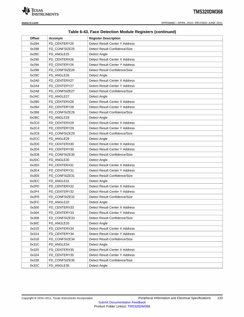
TMS320DM368
www.ti.com SPRS668C–APRIL 2010–REVISED JUNE 2011
Table 6-43. Face Detection Module Registers (continued)
Offset Acronym Register Description
0x284 FD_CENTERY25 Detect Result Center Y Address
0x288 FD_CONFSIZE25 Detect Result Confidence/Size
0x28C FD_ANGLE25 Detect Angle
0x290 FD_CENTERX26 Detect Result Center X Address
0x294 FD_CENTERY26 Detect Result Center Y Address
0x298 FD_CONFSIZE26 Detect Result Confidence/Size
0x29C FD_ANGLE26 Detect Angle
0x2A0 FD_CENTERX27 Detect Result Center X Address
0x2A4 FD_CENTERY27 Detect Result Center Y Address
0x2A8 FD_CONFSIZE27 Detect Result Confidence/Size
0x2AC FD_ANGLE27 Detect Angle
0x2B0 FD_CENTERX28 Detect Result Center X Address
0x2B4 FD_CENTERY28 Detect Result Center Y Address
0x2B8 FD_CONFSIZE28 Detect Result Confidence/Size
0x2BC FD_ANGLE28 Detect Angle
0x2C0 FD_CENTERX29 Detect Result Center X Address
0x2C4 FD_CENTERY29 Detect Result Center Y Address
0x2C8 FD_CONFSIZE29 Detect Result Confidence/Size
0x2CC FD_ANGLE29 Detect Angle
0x2D0 FD_CENTERX30 Detect Result Center X Address
0x2D4 FD_CENTERY30 Detect Result Center Y Address
0x2D8 FD_CONFSIZE30 Detect Result Confidence/Size
0x2DC FD_ANGLE30 Detect Angle
0x2E0 FD_CENTERX31 Detect Result Center X Address
0x2E4 FD_CENTERY31 Detect Result Center Y Address
0x2E8 FD_CONFSIZE31 Detect Result Confidence/Size
0x2EC FD_ANGLE31 Detect Angle
0x2F0 FD_CENTERX32 Detect Result Center X Address
0x2F4 FD_CENTERY32 Detect Result Center Y Address
0x2F8 FD_CONFSIZE32 Detect Result Confidence/Size
0x2FC FD_ANGLE32 Detect Angle
0x300 FD_CENTERX33 Detect Result Center X Address
0x304 FD_CENTERY33 Detect Result Center Y Address
0x308 FD_CONFSIZE33 Detect Result Confidence/Size
0x30C FD_ANGLE33 Detect Angle
0x310 FD_CENTERX34 Detect Result Center X Address
0x314 FD_CENTERY34 Detect Result Center Y Address
0x318 FD_CONFSIZE34 Detect Result Confidence/Size
0x31C FD_ANGLE34 Detect Angle
0x320 FD_CENTERX35 Detect Result Center X Address
0x324 FD_CENTERY35 Detect Result Center Y Address
0x328 FD_CONFSIZE35 Detect Result Confidence/Size
0x32C FD_ANGLE35 Detect Angle
Copyright © 2010–2011, Texas Instruments Incorporated Peripheral Information and Electrical Specifications 133Submit Documentation Feedback
Product Folder Link(s): TMS320DM368

PCLK
2
1
3
4
4
TMS320DM368
SPRS668C–APRIL 2010–REVISED JUNE 2011 www.ti.com
6.12.1.5 VPFE Electrical Data/Timing
Table 6-44. Timing Requirements for VPFE PCLK Master/Slave Mode (1) (see Figure 6-31)
NO. MIN MAX UNIT
Slave Mode 8.33 120 ns1 tc(PCLK) Cycle time, PCLK
Master Mode 13.33 120 ns
2 tw(PCLKH) Pulse duration, PCLK high tc(PCLK)* 0.35 tc(PCLK)* 0.65 ns
3 tw(PCLKL) Pulse duration, PCLK low tc(PCLK)* 0.35 tc(PCLK)* 0.65 ns
4 tt(PCLK) Transition time, PCLK 2 ns
(1) P = 1/SYSCLK4 in nanoseconds (ns). For example, if the SYSCLK4 frequency is 135 MHz, use P = 7.41 ns. See Section 3.3, DeviceClocking, for more information on the supported clock configurations of the device.
Figure 6-31. VPFE PCLK Timing
Table 6-45. Timing Requirements for VPFE (ISIF) Slave Mode (see Figure 6-32)
DEVICE UNINO. TMIN MAX
Positive Edge 2.5tsu(DATAV-5 Setup time, ISIF DATA valid before PCLK edge nsPCLK) Negative Edge 1.5
Positive Edge 1.56 th(PCLK-DATAV) Hold time, ISIF DATA valid after PCLK edge ns
Negative Edge 2.5
Positive Edge 2.57 tsu(HDV-PCLK) Setup time, HD valid before PCLK edge ns
Negative Edge 1.5
Positive Edge 1.58 th(PCLK-HDV) Hold time, HD valid after PCLK edge ns
Negative Edge 2.5
Positive Edge 2.59 tsu(VDV-PCLK) Setup time, VD valid before PCLK edge ns
Negative Edge 1.5
Positive Edge 1.510 th(PCLK-VDV) Hold time, VD valid after PCLK edge ns
Negative Edge 2.5
Positive Edge 2.5tsu(C_WEV-11 Setup time, C_WE valid before PCLK edge nsPCLK) Negative Edge 1.5
Positive Edge 1.512 th(PCLK-C_WEV) Hold time, C_WE valid after PCLK edge ns
Negative Edge 2.5
Positive Edge 2.5tsu(C_FIELDV-13 Setup time, C_FIELD valid before PCLK edge nsPCLK) Negative Edge 1.5
Positive Edge 1.5th(PCLK-14 Hold time, C_FIELD valid after PCLK edge nsC_FIELDV) Negative Edge 2.5
134 Peripheral Information and Electrical Specifications Copyright © 2010–2011, Texas Instruments Incorporated
Submit Documentation FeedbackProduct Folder Link(s): TMS320DM368

PCLK(Positive Edge Clocking)
PCLK(Negative Edge Clocking)
7, 9
HD/VD
CIN[7:0]/YIN[7:0]/
CCD[15:0]
8, 10
11, 13
12, 14
5
6
C_WE/C_FIELD
PCLK(Positive Edge Clocking)
1516
2324
CIN[7:0]/YIN[7:0]/CCD[15:0]
C_WE/C_FIELD
PCLK(Positive Edge Clocking)
TMS320DM368
www.ti.com SPRS668C–APRIL 2010–REVISED JUNE 2011
Figure 6-32. VPFE (ISIF) Slave Mode Input Data Timing
Table 6-46. Timing Requirements for VPFE (ISIF) Master Mode (1) (see Figure 6-33)
DEVICE UNINO. TMIN MAX
Positive Edge 2.5tsu(DATAV-15 Setup time, ISIF DATA valid before PCLK edge nsPCLK) Negative Edge 1.5
Positive Edge 1.516 th(PCLK-DATAV) Hold time, ISIF DATA valid after PCLK edge ns
Negative Edge 2.5
Positive Edge 2.523 tsu(CWEV-PCLK) Setup time, C_WE valid before PCLK edge ns
Negative Edge 1.5
Positive Edge 1.524 th(PCLK-CWEV) Hold time, C_WE valid after PCLK edge ns
Negative Edge 2.5
(1) The VPFE may be configured to operate in either positive or negative edge clocking mode. When in positive edge clocking mode therising edge of PCLK is referenced. When in negative edge clocking mode the falling edge of PCLK is referenced.
Figure 6-33. VPFE (ISIF) Master Mode Input Data Timing
Copyright © 2010–2011, Texas Instruments Incorporated Peripheral Information and Electrical Specifications 135Submit Documentation Feedback
Product Folder Link(s): TMS320DM368

PCLK
(Positive Edge Clocking)18
20
HD
VD
PCLK
(Negative Edge Clocking)
TMS320DM368
SPRS668C–APRIL 2010–REVISED JUNE 2011 www.ti.com
Table 6-47. Switching Characteristics Over Recommended Operating Conditions for VPFE (ISIF) MasterMode (see Figure 6-34)
DEVICENO. PARAMETER UNIT
MIN MAX
18 td(PCLKL-HDIV) Delay time, PCLK edge to HD valid 1.5 11 ns
20 td(PCLKL-VDIV) Delay time, PCLK edge to VD valid 1.5 11 ns
Figure 6-34. VPFE (ISIF) Master Mode Control Output Data Timing
6.12.2 Video Processing Back-End (VPBE)
The Video Processing Back-End of VPBE module is comprised of the On Screen Display (OSD) moduleand the Video Encoder / Digital LCD Controller (VENC/DLCD).
Table 6-48 lists the Video Processing Back-End (VPBE) module registers, their corresponding acronyms,and the device memory locations (offsets).
Table 6-48. VPBE Module Register Map
Address Peripheral Description
0x01C7:0200 VPBE_CLK_CTRL VPBE Clock Control
0x01C7:1C00 OSD VPBE On-Screen Display
0x01C7:1E00 VENC VPBE Video Encoder
6.12.2.1 On-Screen Display (OSD)
The primary function of the OSD module is to gather and blend video data and display/bitmap data andthen pass it to the Video Encoder (VENC) in YCbCr format. The video and display data is read fromexternal DDR2/mDDR memory. The OSD is programmed via control and parameter registers. Thefollowing are the primary features that are supported by the OSD.• Support for two video windows and two OSD bitmapped windows that can be displayed simultaneously
(VIDWIN0/VIDWIN1 and OSDWIN0/OSDWIN1).• Video windows support YCbCr data in 422 and 420 formats from external memory, with the ability to
interchange the order of the CbCr component in the 32-bit word• OSD bitmap windows support = 4/8 bit width index data of color palette• In addition one OSD bitmap window at a time can be configured to one of the following:
– YUV422 (same as video data)– RGB format data in 16-bit mode (R=5bit, G=6bit, B=5bit)– 24-bit mode (each R/G/B=8bit) with pixel level blending with video windows
• Programmable color palette with the ability to select between a RAM/ROM table with support for 256colors.
• Support for 2 ROM tables, one of which can be selected at a given time• Separate enable/disable control for each window• Programmable width, height, and base starting coordinates for each window
136 Peripheral Information and Electrical Specifications Copyright © 2010–2011, Texas Instruments Incorporated
Submit Documentation FeedbackProduct Folder Link(s): TMS320DM368

TMS320DM368
www.ti.com SPRS668C–APRIL 2010–REVISED JUNE 2011
• External memory address and offset registers for each window• Support for x2 and x4 zoom in both the horizontal and vertical direction• Pixel-level blending/transparency/blinking attributes can be defined for OSDWIN0 when OSDWIN1 is
configured as an attribute window for OSDWIN0.• Support for blinking intervals to the attribute window• Ability to select either field/frame mode for the windows (interlaced/progressive)• An eight step blending process between the bitmap and video windows• Transparency support for the bitmap and video data (when a bitmap pixel is zero, there will be no
blending for that corresponding video pixel)• Ability to resize from VGA to NTSC/PAL (640x480 to 720x576) for both the OSD and video windows• Horizontal rescaling x1.5 is supported• Support for a rectangular cursor window and a programmable background color selection.• The width, height, and color of the cursor is selectable• The display priority is: Rectangular-Cursor > OSDWIN1 > OSDWIN0 > VIDWIN1 > VIDWIN0 >
background color• Support for attenuation of the YCbCr values for the REC601 standard.
The following restrictions exist in the OSD module.• If the vertical resize filter is enabled for either of the video windows, the maximum horizontal window
dimension cannot be greater than 1024 currently. This is due to the limitation in the size of the linememory.
• It is not possible to use both of the CLUT ROMs at the same time. However, a window can use RAMwhile another uses ROM.
Table 6-49 lists the On-Screen Display (OSD) registers, their corresponding acronyms, and the devicememory locations (offsets).
Table 6-49. On-Screen Display (OSD) Registers
Offset Acronym Register Description
0h MODE OSD Mode Setup
4h VIDWINMD Video Window Mode Setup
8h OSDWIN0MD Bitmap Window 0 Mode Setup
Ch OSDWIN1MD OSD Window 1 Mode Setup(when used as a second OSD window)
Ch OSDATRMD OSD Attribute Window Mode Setup(when used as an attribute window)
10h RECTCUR Rectangular Cursor Setup
14h RSV0 Reserved
18h VIDWIN0OFST Video Window 0 Offset
1Ch VIDWIN1OFST Video Window 1 Offset
20h OSDWIN0OFST Bitmap Window 0 Offset
24h OSDWIN1OFST Bitmap Window 1/Attribute Window Offset
28h VIDWINADH Video Window 0/1 Address - High
2Ch VIDWIN0ADL Video Window 0 Address - Low
30h VIDWIN1ADL Video Window 1 Address - Low
34h OSDWINADH BMP Window 0/1 Address - High
38h OSDWIN0ADL BMP Window 0 Address - Low
3Ch OSDWIN1ADL Bitmap Window 1/Attribute Address - Low
40h BASEPX Base Pixel X
44h BASEPY Base Pixel Y
48h VIDWIN0XP Video Window 0 X-Position
Copyright © 2010–2011, Texas Instruments Incorporated Peripheral Information and Electrical Specifications 137Submit Documentation Feedback
Product Folder Link(s): TMS320DM368

TMS320DM368
SPRS668C–APRIL 2010–REVISED JUNE 2011 www.ti.com
Table 6-49. On-Screen Display (OSD) Registers (continued)
Offset Acronym Register Description
4Ch VIDWIN0YP Video Window 0 Y-Position
50h VIDWIN0XL Video Window 0 X-Size
54h VIDWIN0YL Video Window 0 Y-Size
58h VIDWIN1XP Video Window 1 X-Position
5Ch VIDWIN1YP Video Window 1 Y-Position
60h VIDWIN1XL Video Window 1 X-Size
64h VIDWIN1YL Video Window 1 Y-Size
68h OSDWIN0XP Bitmap Window 0 X-Position
6Ch OSDWIN0YP Bitmap Window 0 Y-Position
70h OSDWIN0XL Bitmap Window 0 X-Size
74h OSDWIN0YL Bitmap Window 0 Y-Size
78h OSDWIN1XP Bitmap Window 1 X-Position
7Ch OSDWIN1YP Bitmap Window 1 Y-Position
80h OSDWIN1XL Bitmap Window 1 X-Size
84h OSDWIN1YL Bitmap Window 1 Y-Size
88h CURXP Rectangular Cursor Window X-Position
8Ch CURYP Rectangular Cursor Window Y-Position
90h CURXL Rectangular Cursor Window X-Size
94h CURYL Rectangular Cursor Window Y-Size
98h RSV1 Reserved
9Ch RSV2 Reserved
A0h W0BMP01 Window 0 Bitmap Value to Palette Map 0/1
A4h W0BMP23 Window 0 Bitmap Value to Palette Map 2/3
A8h W0BMP45 Window 0 Bitmap Value to Palette Map 4/5
ACh W0BMP67 Window 0 Bitmap Value to Palette Map 6/7
B0h W0BMP89 Window 0 Bitmap Value to Palette Map 8/9
B4h W0BMPAB Window 0 Bitmap Value to Palette Map A/B
B8h W0BMPCD Window 0 Bitmap Value to Palette Map C/D
BCh W0BMPEF Window 0 Bitmap Value to Palette Map E/F
C0h W1BMP01 Window 1 Bitmap Value to Palette Map 0/1
C4h W1BMP23 Window 1 Bitmap Value to Palette Map 2/3
C8h W1BMP45 Window 1 Bitmap Value to Palette Map 4/5
CCh W1BMP67 Window 1 Bitmap Value to Palette Map 6/7
D0h W1BMP89 Window 1 Bitmap Value to Palette Map 8/9
D4h W1BMPAB Window 1 Bitmap Value to Palette Map A/B
D8h W1BMPCD Window 1 Bitmap Value to Palette Map C/D
DCh W1BMPEF Window 1 Bitmap Value to Palette Map E/F
E0h VBNDRY Test Mode
E4h EXTMODE Extended Mode
E8h MISCCTL Miscellaneous Control
ECh CLUTRAMYCB CLUT RAM Y/Cb Setup
F0h CLUTRAMCR CLUT RAM Cr/Mapping Setup
F4h TRANSPVALL Transparent Color Code - Lower
F8h TRANSPVALU Transparent Color Code - Upper
FCh TRANSPBMPIDX Transparent Index Code for Bitmaps
138 Peripheral Information and Electrical Specifications Copyright © 2010–2011, Texas Instruments Incorporated
Submit Documentation FeedbackProduct Folder Link(s): TMS320DM368

TMS320DM368
www.ti.com SPRS668C–APRIL 2010–REVISED JUNE 2011
6.12.2.2 Video Encoder / Digital LCD Controller (VENC/DLCD)
The VENC/DLCD consists of three major blocks:• Video encoder to generate analog video output• Digital LCD controller to generate digital RGB/YCbCr data output and timing signals• Timing generator
The video encoder for analog video supports the following features:• Master Clock Input - 27 MHz or 74.25 MHz• SDTV Support
– Composite NTSC-M, PAL-B/D/G/H/I– S-Video (Y/C)– Component YPbPr– RGB– CGMS/WSS– Closed Caption
• HDTV Support– 525p/625p/720p/1080i– Component YPbPr– RGB– CGMS/WSS
• Master/Slave Operation• Three 10-bit D/A Converters
The digital LCD controller supports the following features:• Programmable Timing Generator• Various Output Formats
– YCbCr 4:2:2 16-bit– YCbCr 4:2:2 8-bit– Parallel RGB 16/18/24-bit– Serial RGB 8-bit
• EAV/SAV insertion• Master/Slave Operation
Table 6-50 lists the Video Encoder / Digital LCD Controller (VENC/DLCD) registers, their correspondingacronyms, and the device memory locations (offsets).
Table 6-50. Video Encoder (VENC) Registers
Offset Acronym Register Description
0h VMOD Video Mode
4h VIOCTL Video Interface I/O Control
8h VDPRO Video Data Processing
Ch SYNCCTL Sync Control
10h HSPLS Horizontal Sync Pulse Width
14h VSPLS Vertical Sync Pulse Width
18h HINTVL Horizontal Interval
1Ch HSTART Horizontal Valid Data Start Position
20h HVALID Horizontal Data Valid Range
24h VINTVL Vertical Interval
28h VSTART Vertical Valid Data Start Position
Copyright © 2010–2011, Texas Instruments Incorporated Peripheral Information and Electrical Specifications 139Submit Documentation Feedback
Product Folder Link(s): TMS320DM368

TMS320DM368
SPRS668C–APRIL 2010–REVISED JUNE 2011 www.ti.com
Table 6-50. Video Encoder (VENC) Registers (continued)
Offset Acronym Register Description
2Ch VVALID Vertical Data Valid Range
30h HSDLY Horizontal Sync Delay
34h VSDLY Vertical Sync Delay
38h YCCCTL YCbCr Control
3Ch RGBCTL RGB Control
40h RGBCLP RGB Level Clipping
44h LINECTL Line ID Control
48h CULLLINE Culling Line Control
4Ch LCDOUT LCD Output Signal Control
50h BRT0 Brightness Start Position Signal Control
54h BRT1 Brightness Width Signal Control
58h ACCTL LCD_AC Signal Control
5Ch PWM0 PWM Output Period
60h PWM1 PWM Output Pulse Width
64h DCLKCTL DCLK Control
68h DCLKPTN0 DCLK Pattern 0
6Ch DCLKPTN1 DCLK Pattern 1
70h DCLKPTN2 DCLK Pattern 2
74h DCLKPTN3 DCLK Pattern 3
78h DCLKPTN0A DCLK Auxiliary Pattern 0
7Ch DCLKPTN1A DCLK Auxiliary Pattern 1
80h DCLKPTN2A DCLK Auxiliary Pattern 2
84h DCLKPTN3A DCLK Auxiliary Pattern 3
88h DCLKHSTT Horizontal DCLK Mask Start Position
8Ch DCLKHSTTA Horizontal Auxiliary DCLK Mask Start Position
90h DCLKHVLD Horizontal DCLK Mask Range
94h DCLKVSTT Vertical DCLK Mask Start Position
98h DCLKVVLD Vertical DCLK Mask Range
9Ch CAPCTL Closed Caption Control
A0h CAPDO Closed Caption Odd Field Data
A4h CAPDE Closed Caption Even Field Data
A8h ATR0 Video Attribute Data 0
ACh ATR1 Video Attribute Data 1
B0h ATR2 Video Attribute Data 2
B4h RSV0 Reserved 0
B8h VSTAT Video Status
BCh RAMADR GCP/FRC Table RAM Address
C0h RAMPORT GCP/FRC Table RAM Data Port
C4h DACTST DAC Test
C8h YCOLVL YOUT and COUT Levels
CCh SCPROG Sub-Carrier Programming
D0h RSV1 Reserved 1
D4h RSV2 Reserved 2
D8h RSV3 Reserved 3
DCh CVBS Composite Mode
E0h CMPNT Component Mode
E4h ETMG0 CVBS Timing Control 0
140 Peripheral Information and Electrical Specifications Copyright © 2010–2011, Texas Instruments Incorporated
Submit Documentation FeedbackProduct Folder Link(s): TMS320DM368

TMS320DM368
www.ti.com SPRS668C–APRIL 2010–REVISED JUNE 2011
Table 6-50. Video Encoder (VENC) Registers (continued)
Offset Acronym Register Description
E8h ETMG1 CVBS Timing Control 1
ECh ETMG2 CVBS Timing Control 2
F0h ETMG3 CVBS Timing Control 3
F4h DACSEL DAC Output Select
100h ARGBX0 Analog RGB Matrix 0
104h ARGBX1 Analog RGB Matrix 1
108h ARGBX2 Analog RGB Matrix 2
10Ch ARGBX3 Analog RGB Matrix 3
110h ARGBX4 Analog RGB Matrix 4
114h DRGBX0 Digital RGB Matrix 0
118h DRGBX1 Digital RGB Matrix 1
11Ch DRGBX2 Digital RGB Matrix 2
120h DRGBX3 Digital RGB Matrix 3
124h DRGBX4 Digital RGB Matrix 4
128h VSTARTA Vertical Data Valid Start Position For Even Field
12Ch OSDCLK0 OSD Clock Control 0
130h OSDCLK1 OSD Clock Control 1
134h HVLDCL0 Horizontal Valid Culling Control 0
138h HVLDCL1 Horizontal Valid Culling Control 1
13Ch OSDHADV OSD Horizontal Sync Advance
140h CLKCTL Clock Control
144h GAMCTL Enable Gamma Correction
148h VVALIDA Vertical Data Valid Area For Even Field
14Ch BATR0 Video Attribute 0 For Type B Packet
150h BATR1 Video Attribute 1 For Type B Packet
154h BATR2 Video Attribute 2 For Type B Packet
158h BATR3 Video Attribute 3 For Type B Packet
15Ch BATR4 Video Attribute 4 For Type B Packet
160h BATR5 Video Attribute 5 For Type B Packet
164h BATR6 Video Attribute 6 For Type B Packet
168h BATR7 Video Attribute 7 For Type B Packet
16Ch BATR8 Video Attribute 8 For Type B Packet
170h DACAMP Gain and Offset
6.12.2.3 VPBE Electrical Data/Timing
Table 6-51. Timing Requirements for VPBE CLK Inputs (see Figure 6-35)
DEVICENO. UNIT
MIN MAX
1 tc(PCLK) Cycle time, PCLK (1) 13.33 160 ns
2 tw(PCLKH) Pulse duration, PCLK high 5.7 ns
3 tw(PCLKL) Pulse duration, PCLK low 5.7 ns
4 tt(PCLK) Transition time, PCLK 3 ns
5 tc(EXTCLK) Cycle time, EXTCLK 13.33 160 ns
6 tw(EXTCLKH) Pulse duration, EXTCLK high 5.7 ns
7 tw(EXTCLKL) Pulse duration, EXTCLK low 5.7 ns
(1) For timing specifications relating to PCLK see Table 6-44, Timing Requirements for VPFE PCLK Master/Slave Mode.
Copyright © 2010–2011, Texas Instruments Incorporated Peripheral Information and Electrical Specifications 141Submit Documentation Feedback
Product Folder Link(s): TMS320DM368

1
PCLK
2
3
75
64
8
EXTCLK
4
8
VCLKIN(A)
(Positive Edge Clocking)
9
VCLKIN(A)
(Negative Edge Clocking)
10
VCTL(B)
A. VCLKIN = PCLK or EXTCLK. Note Positive and Negative edge apply for PCLK only, EXTCLK does not support negative edge clocking.
B. VCTL = HSYNC, VSYNC, and FIELD
TMS320DM368
SPRS668C–APRIL 2010–REVISED JUNE 2011 www.ti.com
Table 6-51. Timing Requirements for VPBE CLK Inputs (see Figure 6-35) (continued)
DEVICENO. UNIT
MIN MAX
8 tt(EXTCLK) Transition time, EXTCLK 3 ns
Figure 6-35. VPBE PCLK and EXTCLK Timing
Table 6-52. Timing Requirements for VPBE Control Input With Respect to PCLK and EXTCLK (1) (2) (3) (seeFigure 6-36)
DEVICE UNINO. TMIN MAX
Positive Edge 4tsu(VCTLV- Setup time, VCTL valid before VCLKIN9 nsVCLKIN) edge Negative Edge 3
Positive Edge 1th(VCLKIN-10 Hold time, VCTL valid after VCLKIN edge nsVCTLV) Negative Edge 2
(1) The VPBE may be configured to operate in either positive or negative edge clocking mode. When in positive edge clocking mode, therising edge of VCLKIN is referenced. When in negative edge clocking mode, the falling edge of VCLKIN is referenced.
(2) VCTL = HSYNC, VSYNC, and FIELD(3) VCLKIN = PCLK or EXTCLK. Positive and Negative Edge apply to PCLK only; EXTCLK does not support Negative Edge clocking.
Figure 6-36. VPBE Input Timing With Respect to PCLK and EXTCLK
142 Peripheral Information and Electrical Specifications Copyright © 2010–2011, Texas Instruments Incorporated
Submit Documentation FeedbackProduct Folder Link(s): TMS320DM368

VCLKIN(A)
(Positive Edge Clocking)
13
VCLKIN(A)
(Negative Edge Clocking)
11
VCTL(B)
A. VCLKIN = PCLK or EXTCLK. Note Positive and Negative edge apply for PCLK only, EXTCLK does not support negative edge clocking.
B. VCTL = HSYNC, VSYNC, FIELD, and LCD_OE
C. VDATA = COUT[7:0], YOUT[7:0], R[7:0], G[7:0], and B[7:0]
VDATA(C)
14
12
TMS320DM368
www.ti.com SPRS668C–APRIL 2010–REVISED JUNE 2011
Table 6-53. Switching Characteristics Over Recommended Operating Conditions for VPBE Control andData Output With Respect to PCLK and EXTCLK (1) (2) (3) (see Figure 6-37)
DEVICENO. PARAMETER UNIT
MIN MAX
Positive Edge 15td(VCLKIN-11 Delay time, VCLKIN edge to VCTL valid nsVCTLV) Negative Edge 16
td(VCLKIN-12 Delay time, VCLKIN edge to VCTL invalid 2 nsVCTLIV)
VCLKIN = EXTCLK 15td(VCLKIN-13 Delay time, VCLKIN edge to VDATA valid nsVDATAV) VCLKIN = PCLK 17.5
td(VCLKIN-14 Delay time, VCLKIN edge to VDATA invalid 2 nsVDATAIV)
(1) The VPBE may be configured to operate in either positive or negative edge clocking mode. When in positive edge clocking mode, therising edge of VCLKIN is referenced. When in negative edge clocking mode, the falling edge of VCLKIN is referenced.
(2) VCLKIN = PCLK or EXTCLK. Positive and Negative Edge apply to PCLK only; EXTCLK does not support Negative Edge clocking.(3) VCTL = HSYNC, VSYNC, FIELD, and LCD_OE.
Figure 6-37. VPBE Control and Data Output With Respect to PCLK and EXTCLK
Copyright © 2010–2011, Texas Instruments Incorporated Peripheral Information and Electrical Specifications 143Submit Documentation Feedback
Product Folder Link(s): TMS320DM368
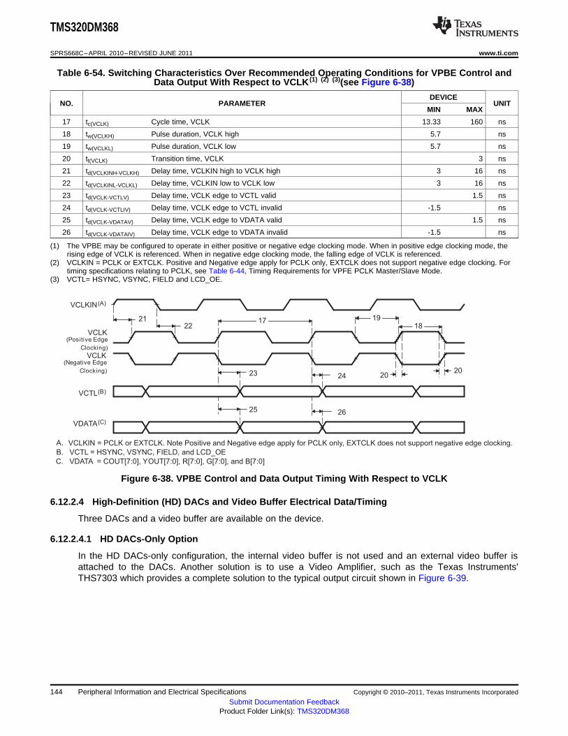
VCLK(Positive Edge
Clocking)
VCLK(Negative Edge
Clocking)
17
VCTL(B)
VDATA(C)
191822
21
23 24
25 26
VCLKIN(A)
A.
B. VCTL = HSYNC, VSYNC, FIELD, and LCD_OE
C. VDATA = COUT[7:0], YOUT[7:0], R[7:0], G[7:0], and B[7:0]
2020
VCLKIN = PCLK or EXTCLK. Note Positive and Negative edge apply for PCLK only, EXTCLK does not support negative edge clocking.
TMS320DM368
SPRS668C–APRIL 2010–REVISED JUNE 2011 www.ti.com
Table 6-54. Switching Characteristics Over Recommended Operating Conditions for VPBE Control andData Output With Respect to VCLK (1) (2) (3)(see Figure 6-38)
DEVICENO. PARAMETER UNIT
MIN MAX
17 tc(VCLK) Cycle time, VCLK 13.33 160 ns
18 tw(VCLKH) Pulse duration, VCLK high 5.7 ns
19 tw(VCLKL) Pulse duration, VCLK low 5.7 ns
20 tt(VCLK) Transition time, VCLK 3 ns
21 td(VCLKINH-VCLKH) Delay time, VCLKIN high to VCLK high 3 16 ns
22 td(VCLKINL-VCLKL) Delay time, VCLKIN low to VCLK low 3 16 ns
23 td(VCLK-VCTLV) Delay time, VCLK edge to VCTL valid 1.5 ns
24 td(VCLK-VCTLIV) Delay time, VCLK edge to VCTL invalid -1.5 ns
25 td(VCLK-VDATAV) Delay time, VCLK edge to VDATA valid 1.5 ns
26 td(VCLK-VDATAIV) Delay time, VCLK edge to VDATA invalid -1.5 ns
(1) The VPBE may be configured to operate in either positive or negative edge clocking mode. When in positive edge clocking mode, therising edge of VCLK is referenced. When in negative edge clocking mode, the falling edge of VCLK is referenced.
(2) VCLKIN = PCLK or EXTCLK. Positive and Negative edge apply for PCLK only, EXTCLK does not support negative edge clocking. Fortiming specifications relating to PCLK, see Table 6-44, Timing Requirements for VPFE PCLK Master/Slave Mode.
(3) VCTL= HSYNC, VSYNC, FIELD and LCD_OE.
Figure 6-38. VPBE Control and Data Output Timing With Respect to VCLK
6.12.2.4 High-Definition (HD) DACs and Video Buffer Electrical Data/Timing
Three DACs and a video buffer are available on the device.
6.12.2.4.1 HD DACs-Only Option
In the HD DACs-only configuration, the internal video buffer is not used and an external video buffer isattached to the DACs. Another solution is to use a Video Amplifier, such as the Texas Instruments'THS7303 which provides a complete solution to the typical output circuit shown in Figure 6-39.
144 Peripheral Information and Electrical Specifications Copyright © 2010–2011, Texas Instruments Incorporated
Submit Documentation FeedbackProduct Folder Link(s): TMS320DM368

COMPY
COMPPB
COMPPR
IREF
VREF
IDACOUT
VFB
TVOUT
RBIAS
TV Monitor
75 Ω
Low-Pass Filter
~R = 75 ΩLOAD
AmplifierGain = 5.6 V/V
75 Ω
75 Ω
DACCH-A
75 Ω
75 Ω
75 Ω
Low-Pass Filter
~R = 75 ΩLOAD
Low-Pass Filter
~R = 75 ΩLOAD
AmplifierGain = 5.6 V/V
AmplifierGain = 5.6 V/V
CBG
0.1 µFDC = 0.5 V
DACCH-B
DACCH-C
TMS320DM368
www.ti.com SPRS668C–APRIL 2010–REVISED JUNE 2011
A. RBIAS = 2400Ω.B. VREF = 0.5V (from external supply).C. IDACOUT must be connected to Vss or left open for proper device configuration.D. VFB must be connected to Vss or left open for proper device configuration.E. TVOUT must be connected to Vss or left open for proper device configuration.
Figure 6-39. HD Video DAC Application Example
6.12.2.4.2 DAC With Video Buffer Option
In a DAC plus video buffer configuration, one of the DACs may be used along with the video buffer forstandard definition TVOUT mode. In the DAC plus video buffer configuration, the DAC and internal videobuffer are both used, and a TV cable may be attached directly to the output of the video buffer.Figure 6-40shows an example of the DAC Plus Video Buffer Option circuit configuration.
Copyright © 2010–2011, Texas Instruments Incorporated Peripheral Information and Electrical Specifications 145Submit Documentation Feedback
Product Folder Link(s): TMS320DM368
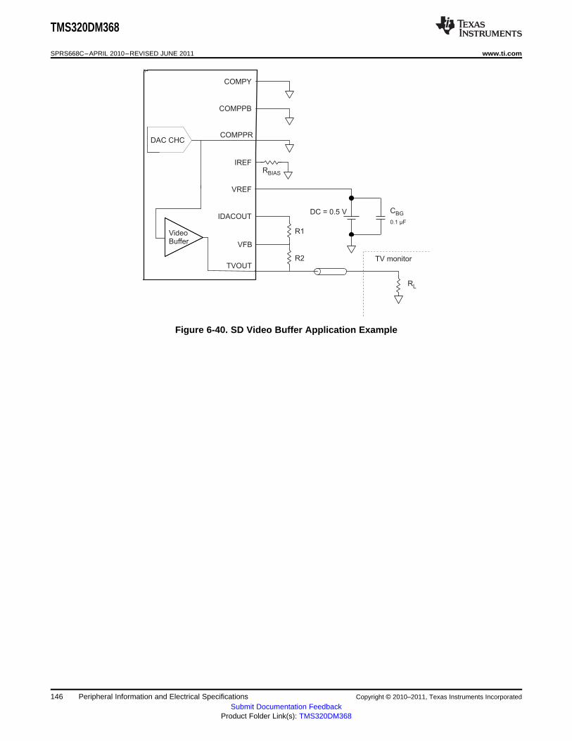
COMPY
COMPPB
COMPPR
IREF
VREF
IDACOUT
VFB
TVOUT
RBIAS
R1
R2 TV monitor
RL
CBG
0.1 µF
DC = 0.5 V
DAC CHC
VideoBuffer
TMS320DM368
SPRS668C–APRIL 2010–REVISED JUNE 2011 www.ti.com
Figure 6-40. SD Video Buffer Application Example
146 Peripheral Information and Electrical Specifications Copyright © 2010–2011, Texas Instruments Incorporated
Submit Documentation FeedbackProduct Folder Link(s): TMS320DM368

TMS320DM368
www.ti.com SPRS668C–APRIL 2010–REVISED JUNE 2011
6.13 USB 2.0
The USB2.0 peripheral supports the following features:• USB 2.0 peripheral at speeds high speed (HS: 480 Mb/s) and full speed (FS: 12 Mb/s)• USB 2.0 host at speeds HS, FS, and low speed (LS: 1.5 Mb/s)• All transfer modes (control, bulk, interrupt, and isochronous)• Four Transmit (TX) and four Receive (RX) endpoints in addition to endpoint 0• FIFO RAM
– 4K bytes shared by all endpoints.– Programmable FIFO size
• Includes a DMA sub-module that supports four TX and four RX channels of CPPI 3.0 DMAs• RNDIS mode for accelerating RNDIS type protocols using short packet termination over USB• USB OTG extensions, i.e. session request protocol (SRP) and host negotiation protocol (HNP)
The USB2.0 peripheral does not support the following features:• On-chip charge pump• High bandwidth ISO mode is not supported (triple buffering)• RNDIS mode acceleration for USB sizes that are not multiples of 64 bytes• Endpoint max USB packet sizes that do not conform to the USB 2.0 spec (for FS/LS: 8, 16, 32, 64,
and 1023 are defined; for HS: 64, 128, 512, and 1024 are defined)
6.13.1 USB Peripheral Register Description(s)
Table 6-55 lists the USB registers, their corresponding acronyms, and the device memory locations(offsets).
Table 6-55. Universal Serial Bus (USB) Registers
Offset Acronym Register Description
4h CTRLR Control Register
8h STATR Status Register
10h RNDISR RNDIS Register
14h AUTOREQ Autorequest Register
20h INTSRCR USB Interrupt Source Register
24h INTSETR USB Interrupt Source Set Register
28h INTCLRR USB Interrupt Source Clear Register
2Ch INTMSKR USB Interrupt Mask Register
30h INTMSKSETR USB Interrupt Mask Set Register
34h INTMSKCLRR USB Interrupt Mask Clear Register
38h INTMASKEDR USB Interrupt Source Masked Register
3Ch EOIR USB End of Interrupt Register
40h INTVECTR USB Interrupt Vector Register
80h TCPPICR Transmit CPPI Control Register
84h TCPPITDR Transmit CPPI Teardown Register
88h TCPPIEOIR Transmit CPPI DMA Controller End of Interrupt Register
8Ch Reserved -
90h TCPPIMSKSR Transmit CPPI Masked Status Register
94h TCPPIRAWSR Transmit CPPI Raw Status Register
98h TCPPIIENSETR Transmit CPPI Interrupt Enable Set Register
9Ch TCPPIIENCLRR Transmit CPPI Interrupt Enable Clear Register
C0h RCPPICR Receive CPPI Control Register
D0h RCPPIMSKSR Receive CPPI Masked Status Register
Copyright © 2010–2011, Texas Instruments Incorporated Peripheral Information and Electrical Specifications 147Submit Documentation Feedback
Product Folder Link(s): TMS320DM368

TMS320DM368
SPRS668C–APRIL 2010–REVISED JUNE 2011 www.ti.com
Table 6-55. Universal Serial Bus (USB) Registers (continued)
Offset Acronym Register Description
D4h RCPPIRAWSR Receive CPPI Raw Status Register
D8h RCPPIENSETR Receive CPPI Interrupt Enable Set Register
DCh RCPPIIENCLRR Receive CPPI Interrupt Enable Clear Register
E0h RBUFCNT0 Receive Buffer Count 0 Register
E4h RBUFCNT1 Receive Buffer Count 1 Register
E8h RBUFCNT2 Receive Buffer Count 2 Register
ECh RBUFCNT3 Receive Buffer Count 3 Register
Transmit/Receive CPPI Channel 0 State Block
100h TCPPIDMASTATEW0 Transmit CPPI DMA State Word 0
104h TCPPIDMASTATEW1 Transmit CPPI DMA State Word 1
108h TCPPIDMASTATEW2 Transmit CPPI DMA State Word 2
10Ch TCPPIDMASTATEW3 Transmit CPPI DMA State Word 3
110h TCPPIDMASTATEW4 Transmit CPPI DMA State Word 4
114h TCPPIDMASTATEW5 Transmit CPPI DMA State Word 5
11Ch TCPPICOMPPTR Transmit CPPI Completion Pointer
120h RCPPIDMASTATEW0 Receive CPPI DMA State Word 0
124h RCPPIDMASTATEW1 Receive CPPI DMA State Word 1
128h RCPPIDMASTATEW2 Receive CPPI DMA State Word 2
12Ch RCPPIDMASTATEW3 Receive CPPI DMA State Word 3
130h RCPPIDMASTATEW4 Receive CPPI DMA State Word 4
134h RCPPIDMASTATEW5 Receive CPPI DMA State Word 5
138h RCPPIDMASTATEW6 Receive CPPI DMA State Word 6
13Ch RCPPICOMPPTR Receive CPPI Completion Pointer
Transmit/Receive CPPI Channel 1 State Block
140h TCPPIDMASTATEW0 Transmit CPPI DMA State Word 0
144h TCPPIDMASTATEW1 Transmit CPPI DMA State Word 1
148h TCPPIDMASTATEW2 Transmit CPPI DMA State Word 2
14Ch TCPPIDMASTATEW3 Transmit CPPI DMA State Word 3
150h TCPPIDMASTATEW4 Transmit CPPI DMA State Word 4
154h TCPPIDMASTATEW5 Transmit CPPI DMA State Word 5
15Ch TCPPICOMPPTR Transmit CPPI Completion Pointer
160h RCPPIDMASTATEW0 Receive CPPI DMA State Word 0
164h RCPPIDMASTATEW1 Receive CPPI DMA State Word 1
168h RCPPIDMASTATEW2 Receive CPPI DMA State Word 2
16Ch RCPPIDMASTATEW3 Receive CPPI DMA State Word 3
170h RCPPIDMASTATEW4 Receive CPPI DMA State Word 4
174h RCPPIDMASTATEW5 Receive CPPI DMA State Word 5
178h RCPPIDMASTATEW6 Receive CPPI DMA State Word 6
17Ch RCPPICOMPPTR Receive CPPI Completion Pointer
Transmit/Receive CPPI Channel 2 State Block
180h TCPPIDMASTATEW0 Transmit CPPI DMA State Word 0
184h TCPPIDMASTATEW1 Transmit CPPI DMA State Word 1
188h TCPPIDMASTATEW2 Transmit CPPI DMA State Word 2
18Ch TCPPIDMASTATEW3 Transmit CPPI DMA State Word 3
190h TCPPIDMASTATEW4 Transmit CPPI DMA State Word 4
194h TCPPIDMASTATEW5 Transmit CPPI DMA State Word 5
19Ch TCPPICOMPPTR Transmit CPPI Completion Pointer
148 Peripheral Information and Electrical Specifications Copyright © 2010–2011, Texas Instruments Incorporated
Submit Documentation FeedbackProduct Folder Link(s): TMS320DM368
TMS320DM368
www.ti.com SPRS668C–APRIL 2010–REVISED JUNE 2011
Table 6-55. Universal Serial Bus (USB) Registers (continued)
Offset Acronym Register Description
1A0h RCPPIDMASTATEW0 Receive CPPI DMA State Word 0
1A4h RCPPIDMASTATEW1 Receive CPPI DMA State Word 1
1A8h RCPPIDMASTATEW2 Receive CPPI DMA State Word 2
1ACh RCPPIDMASTATEW3 Receive CPPI DMA State Word 3
1B0h RCPPIDMASTATEW4 Receive CPPI DMA State Word 4
1B4h RCPPIDMASTATEW5 Receive CPPI DMA State Word 5
1B8h RCPPIDMASTATEW6 Receive CPPI DMA State Word 6
1BCh RCPPICOMPPTR Receive CPPI Completion Pointer
Transmit/Receive CPPI Channel 3 State Block
1C0h TCPPIDMASTATEW0 Transmit CPPI DMA State Word 0
1C4h TCPPIDMASTATEW1 Transmit CPPI DMA State Word 1
1C8h TCPPIDMASTATEW2 Transmit CPPI DMA State Word 2
1CCh TCPPIDMASTATEW3 Transmit CPPI DMA State Word 3
1D0h TCPPIDMASTATEW4 Transmit CPPI DMA State Word 4
1D4h TCPPIDMASTATEW5 Transmit CPPI DMA State Word 5
1DCh TCPPICOMPPTR Transmit CPPI Completion Pointer
1E0h RCPPIDMASTATEW0 Receive CPPI DMA State Word 0
1E4h RCPPIDMASTATEW1 Receive CPPI DMA State Word 1
1E8h RCPPIDMASTATEW2 Receive CPPI DMA State Word 2
1ECh RCPPIDMASTATEW3 Receive CPPI DMA State Word 3
1F0h RCPPIDMASTATEW4 Receive CPPI DMA State Word 4
1F4h RCPPIDMASTATEW5 Receive CPPI DMA State Word 5
1F8h RCPPIDMASTATEW6 Receive CPPI DMA State Word 6
1FCh RCPPICOMPPTR Receive CPPI Completion Pointer
Common USB Registers
400h FADDR Function Address Register
401h POWER Power Management Register
402h INTRTX Interrupt Register for Endpoint 0 plus Transmit Endpoints 1 to 4
404h INTRRX Interrupt Register for Receive Endpoints 1 to 4
406h INTRTXE Interrupt enable register for INTRTX
408h INTRRXE Interrupt Enable Register for INTRRX
40Ah INTRUSB Interrupt Register for Common USB Interrupts
40Bh INTRUSBE Interrupt Enable Register for INTRUSB
40Ch FRAME Frame Number Register
40Eh INDEX Index Register for Selecting the Endpoint Status and Control Registers
40Fh TESTMODE Register to Enable the USB 2.0 Test Modes
Indexed RegistersThese registers operate on the endpoint selected by the INDEX register
410h TXMAXP Maximum Packet Size for Peripheral/Host Transmit Endpoint.(Index register set to select Endpoints 1-4)
412h PERI_CSR0 Control Status Register for Endpoint 0 in Peripheral Mode.(Index register set to select Endpoint 0)
HOST_CSR0 Control Status Register for Endpoint 0 in Host Mode.(Index register set to select Endpoint 0)
PERI_TXCSR Control Status Register for Peripheral Transmit Endpoint.(Index register set to select Endpoints 1-4)
HOST_TXCSR Control Status Register for Host Transmit Endpoint.(Index register set to select Endpoints 1-4)
Copyright © 2010–2011, Texas Instruments Incorporated Peripheral Information and Electrical Specifications 149Submit Documentation Feedback
Product Folder Link(s): TMS320DM368

TMS320DM368
SPRS668C–APRIL 2010–REVISED JUNE 2011 www.ti.com
Table 6-55. Universal Serial Bus (USB) Registers (continued)
Offset Acronym Register Description
414h RXMAXP Maximum Packet Size for Peripheral/Host Receive Endpoint.(Index register set to select Endpoints 1-4)
416h PERI_RXCSR Control Status Register for Peripheral Receive Endpoint.(Index register set to select Endpoints 1-4)
HOST_RXCSR Control Status Register for Host Receive Endpoint.(Index register set to select Endpoints 1-4)
418h COUNT0 Number of Received Bytes in Endpoint 0 FIFO.(Index register set to select Endpoint 0)
RXCOUNT Number of Bytes in Host Receive Endpoint FIFO.(Index register set to select Endpoints 1- 4)
41Ah HOST_TYPE0 Defines the speed of Endpoint 0
HOST_TXTYPE Sets the operating speed, transaction protocol and peripheral endpoint number forthe host Transmit endpoint.(Index register set to select Endpoints 1-4)
41Bh HOST_NAKLIMIT0 Sets the NAK response timeout on Endpoint 0.(Index register set to select Endpoint 0)
HOST_TXINTERVAL Sets the polling interval for Interrupt/ISOC transactions or the NAK responsetimeout on Bulk transactions for host Transmit endpoint. (Index register set toselect Endpoints 1-4)
41Ch HOST_RXTYPE Sets the operating speed, transaction protocol and peripheral endpoint number forthe host Receive endpoint.(Index register set to select Endpoints 1-4)
41Dh HOST_RXINTERVAL Sets the polling interval for Interrupt/ISOC transactions or the NAK responsetimeout on Bulk transactions for host Receive endpoint. (Index register set to selectEndpoints 1-4)
41Fh CONFIGDATA Returns details of core configuration. (Index register set to select Endpoint 0)
FIFOn
420h FIFO0 Transmit and Receive FIFO Register for Endpoint 0
424h FIFO1 Transmit and Receive FIFO Register for Endpoint 1
428h FIFO2 Transmit and Receive FIFO Register for Endpoint 2
42Ch FIFO3 Transmit and Receive FIFO Register for Endpoint 3
430h FIFO4 Transmit and Receive FIFO Register for Endpoint 4
OTG Device Control
460h DEVCTL OTG Device Control Register
Dynamic FIFO Control
462h TXFIFOSZ Transmit Endpoint FIFO Size(Index register set to select Endpoints 1-4)
463h RXFIFOSZ Receive Endpoint FIFO Size(Index register set to select Endpoints 1-4)
464h TXFIFOADDR Transmit Endpoint FIFO Address(Index register set to select Endpoints 1-4)
466h RXFIFOADDR Receive Endpoint FIFO Address(Index register set to select Endpoints 1-4)
Target Endpoint 0 Control Registers, Valid Only in Host Mode
480h TXFUNCADDR Address of the target function that has to be accessed through the associatedTransmit Endpoint.
482h TXHUBADDR Address of the hub that has to be accessed through the associated TransmitEndpoint. This is used only when full speed or low speed device is connected via aUSB2.0 high-speed hub.
483h TXHUBPORT Port of the hub that has to be accessed through the associated Transmit Endpoint.This is used only when full speed or low speed device is connected via a USB2.0high-speed hub.
484h RXFUNCADDR Address of the target function that has to be accessed through the associatedReceive Endpoint.
150 Peripheral Information and Electrical Specifications Copyright © 2010–2011, Texas Instruments Incorporated
Submit Documentation FeedbackProduct Folder Link(s): TMS320DM368

TMS320DM368
www.ti.com SPRS668C–APRIL 2010–REVISED JUNE 2011
Table 6-55. Universal Serial Bus (USB) Registers (continued)
Offset Acronym Register Description
486h RXHUBADDR Address of the hub that has to be accessed through the associated ReceiveEndpoint. This is used only when full speed or low speed device is connected via aUSB2.0 high-speed hub.
487h RXHUBPORT Port of the hub that has to be accessed through the associated Receive Endpoint.This is used only when full speed or low speed device is connected via a USB2.0high-speed hub.
Target Endpoint 1 Control Registers, Valid Only in Host Mode
488h TXFUNCADDR Address of the target function that has to be accessed through the associatedTransmit Endpoint.
48Ah TXHUBADDR Address of the hub that has to be accessed through the associated TransmitEndpoint. This is used only when full speed or low speed device is connected via aUSB2.0 high-speed hub.
48Bh TXHUBPORT Port of the hub that has to be accessed through the associated Transmit Endpoint.This is used only when full speed or low speed device is connected via a USB2.0high-speed hub.
48Ch RXFUNCADDR Address of the target function that has to be accessed through the associatedReceive Endpoint.
48Eh RXHUBADDR Address of the hub that has to be accessed through the associated ReceiveEndpoint. This is used only when full speed or low speed device is connected via aUSB2.0 high-speed hub.
48Fh RXHUBPORT Port of the hub that has to be accessed through the associated Receive Endpoint.This is used only when full speed or low speed device is connected via a USB2.0high-speed hub.
Target Endpoint 2 Control Registers, Valid Only in Host Mode
490h TXFUNCADDR Address of the target function that has to be accessed through the associatedTransmit Endpoint.
492h TXHUBADDR Address of the hub that has to be accessed through the associated TransmitEndpoint. This is used only when full speed or low speed device is connected via aUSB2.0 high-speed hub.
493h TXHUBPORT Port of the hub that has to be accessed through the associated Transmit Endpoint.This is used only when full speed or low speed device is connected via a USB2.0high-speed hub.
494h RXFUNCADDR Address of the target function that has to be accessed through the associatedReceive Endpoint.
496h RXHUBADDR Address of the hub that has to be accessed through the associated ReceiveEndpoint. This is used only when full speed or low speed device is connected via aUSB2.0 high-speed hub.
497h RXHUBPORT Port of the hub that has to be accessed through the associated Receive Endpoint.This is used only when full speed or low speed device is connected via a USB2.0high-speed hub.
Target Endpoint 3 Control Registers, Valid Only in Host Mode
498h TXFUNCADDR Address of the target function that has to be accessed through the associatedTransmit Endpoint.
49Ah TXHUBADDR Address of the hub that has to be accessed through the associated TransmitEndpoint. This is used only when full speed or low speed device is connected via aUSB2.0 high-speed hub.
49Bh TXHUBPORT Port of the hub that has to be accessed through the associated Transmit Endpoint.This is used only when full speed or low speed device is connected via a USB2.0high-speed hub.
49Ch RXFUNCADDR Address of the target function that has to be accessed through the associatedReceive Endpoint.
49Eh RXHUBADDR Address of the hub that has to be accessed through the associated ReceiveEndpoint. This is used only when full speed or low speed device is connected via aUSB2.0 high-speed hub.
49Fh RXHUBPORT Port of the hub that has to be accessed through the associated Receive Endpoint.This is used only when full speed or low speed device is connected via a USB2.0high-speed hub.
Target Endpoint 4 Control Registers, Valid Only in Host Mode
Copyright © 2010–2011, Texas Instruments Incorporated Peripheral Information and Electrical Specifications 151Submit Documentation Feedback
Product Folder Link(s): TMS320DM368

TMS320DM368
SPRS668C–APRIL 2010–REVISED JUNE 2011 www.ti.com
Table 6-55. Universal Serial Bus (USB) Registers (continued)
Offset Acronym Register Description
4A0h TXFUNCADDR Address of the target function that has to be accessed through the associatedTransmit Endpoint.
4A2h TXHUBADDR Address of the hub that has to be accessed through the associated TransmitEndpoint. This is used only when full speed or low speed device is connected via aUSB2.0 high-speed hub.
4A3h TXHUBPORT Port of the hub that has to be accessed through the associated Transmit Endpoint.This is used only when full speed or low speed device is connected via a USB2.0high-speed hub.
4A4h RXFUNCADDR Address of the target function that has to be accessed through the associatedReceive Endpoint.
4A6h RXHUBADDR Address of the hub that has to be accessed through the associated ReceiveEndpoint. This is used only when full speed or low speed device is connected via aUSB2.0 high-speed hub.
4A7h RXHUBPORT Port of the hub that has to be accessed through the associated Receive Endpoint.This is used only when full speed or low speed device is connected via a USB2.0high-speed hub.
Control and Status Register for Endpoint 0
502h PERI_CSR0 Control Status Register for Endpoint 0 in Peripheral Mode
HOST_CSR0 Control Status Register for Endpoint 0 in Host Mode
508h COUNT0 Number of Received Bytes in Endpoint 0 FIFO
50Ah HOST_TYPE0 Defines the Speed of Endpoint 0
50Bh HOST_NAKLIMIT0 Sets the NAK Response Timeout on Endpoint 0
50Fh CONFIGDATA Returns details of core configuration.
Control and Status Register for Endpoint 1
510h TXMAXP Maximum Packet Size for Peripheral/Host Transmit Endpoint
512h PERI_TXCSR Control Status Register for Peripheral Transmit Endpoint(peripheral mode)
HOST_TXCSR Control Status Register for Host Transmit Endpoint(host mode)
514h RXMAXP Maximum Packet Size for Peripheral/Host Receive Endpoint
516h PERI_RXCSR Control Status Register for Peripheral Receive Endpoint(peripheral mode)
HOST_RXCSR Control Status Register for Host Receive Endpoint(host mode)
518h RXCOUNT Number of Bytes in Host Receive endpoint FIFO
51Ah HOST_TXTYPE Sets the operating speed, transaction protocol and peripheral endpoint number forthe host Transmit endpoint.
51Bh HOST_TXINTERVAL Sets the polling interval for Interrupt/ISOC transactions or the NAK responsetimeout on Bulk transactions for host Transmit endpoint.
51Ch HOST_RXTYPE Sets the operating speed, transaction protocol and peripheral endpoint number forthe host Receive endpoint.
51Dh HOST_RXINTERVAL Sets the polling interval for Interrupt/ISOC transactions or the NAK responsetimeout on Bulk transactions for host Receive endpoint.
Control and Status Register for Endpoint 2
520h TXMAXP Maximum Packet Size for Peripheral/Host Transmit Endpoint
522h PERI_TXCSR Control Status Register for Peripheral Transmit Endpoint(peripheral mode)
HOST_TXCSR Control Status Register for Host Transmit Endpoint(host mode)
524h RXMAXP Maximum Packet Size for Peripheral/Host Receive Endpoint
526h PERI_RXCSR Control Status Register for Peripheral Receive Endpoint(peripheral mode)
HOST_RXCSR Control Status Register for Host Receive Endpoint(host mode)
152 Peripheral Information and Electrical Specifications Copyright © 2010–2011, Texas Instruments Incorporated
Submit Documentation FeedbackProduct Folder Link(s): TMS320DM368

TMS320DM368
www.ti.com SPRS668C–APRIL 2010–REVISED JUNE 2011
Table 6-55. Universal Serial Bus (USB) Registers (continued)
Offset Acronym Register Description
528h RXCOUNT Number of Bytes in Host Receive endpoint FIFO
52Ah HOST_TXTYPE Sets the operating speed, transaction protocol and peripheral endpoint number forthe host Transmit endpoint.
52Bh HOST_TXINTERVAL Sets the polling interval for Interrupt/ISOC transactions or the NAK responsetimeout on Bulk transactions for host Transmit endpoint.
52Ch HOST_RXTYPE Sets the operating speed, transaction protocol and peripheral endpoint number forthe host Receive endpoint.
52Dh HOST_RXINTERVAL Sets the polling interval for Interrupt/ISOC transactions or the NAK responsetimeout on Bulk transactions for host Receive endpoint.
Control and Status Register for Endpoint 3
530h TXMAXP Maximum Packet Size for Peripheral/Host Transmit Endpoint
532h PERI_TXCSR Control Status Register for Peripheral Transmit Endpoint(peripheral mode)
HOST_TXCSR Control Status Register for Host Transmit Endpoint(host mode)
534h RXMAXP Maximum Packet Size for Peripheral/Host Receive Endpoint
536h PERI_RXCSR Control Status Register for Peripheral Receive Endpoint(peripheral mode)
HOST_RXCSR Control Status Register for Host Receive Endpoint(host mode)
538h RXCOUNT Number of Bytes in Host Receive endpoint FIFO
53Ah HOST_TXTYPE Sets the operating speed, transaction protocol and peripheral endpoint number forthe host Transmit endpoint.
53Bh HOST_TXINTERVAL Sets the polling interval for Interrupt/ISOC transactions or the NAK responsetimeout on Bulk transactions for host Transmit endpoint.
53Ch HOST_RXTYPE Sets the operating speed, transaction protocol and peripheral endpoint number forthe host Receive endpoint.
53Dh HOST_RXINTERVAL Sets the polling interval for Interrupt/ISOC transactions or the NAK responsetimeout on Bulk transactions for host Receive endpoint.
Control and Status Register for Endpoint 4
540h TXMAXP Maximum Packet Size for Peripheral/Host Transmit Endpoint
542h PERI_TXCSR Control Status Register for Peripheral Transmit Endpoint(peripheral mode)
HOST_TXCSR Control Status Register for Host Transmit Endpoint(host mode)
544h RXMAXP Maximum Packet Size for Peripheral/Host Receive Endpoint
546h PERI_RXCSR Control Status Register for Peripheral Receive Endpoint(peripheral mode)
HOST_RXCSR Control Status Register for Host Receive Endpoint(host mode)
548h RXCOUNT Number of Bytes in Host Receive endpoint FIFO
54Ah HOST_TXTYPE Sets the operating speed, transaction protocol and peripheral endpoint number forthe host Transmit endpoint.
54Bh HOST_TXINTERVAL Sets the polling interval for Interrupt/ISOC transactions or the NAK responsetimeout on Bulk transactions for host Transmit endpoint.
54Ch HOST_RXTYPE Sets the operating speed, transaction protocol and peripheral endpoint number forthe host Receive endpoint.
54Dh HOST_RXINTERVAL Sets the polling interval for Interrupt/ISOC transactions or the NAK responsetimeout on Bulk transactions for host Receive endpoint.
Copyright © 2010–2011, Texas Instruments Incorporated Peripheral Information and Electrical Specifications 153Submit Documentation Feedback
Product Folder Link(s): TMS320DM368

trtf
VCRS90% VOH
10% VOL
USB_DM
USB_DP
tper − tjr
TMS320DM368
SPRS668C–APRIL 2010–REVISED JUNE 2011 www.ti.com
6.13.2 USB2.0 Electrical Data/Timing
Table 6-56. Switching Characteristics Over Recommended Operating Conditions for USB2.0 (seeFigure 6-41)
DEVICE
LOW SPEED FULL SPEED HIGH SPEED (1)NO. PARAMETER UNIT1.5 Mbps 12 Mbps 480 Mbps
MIN MAX MIN MAX MIN MAX
1 tr(D) Rise time, USB_DP and USB_DM signals (2) 75 300 4 20 0.5 20 ns
2 tf(D) Fall time, USB_DP and USB_DM signals (2) 75 300 4 20 0.5 20 ns
3 tfrfm Rise/Fall time, matching (3) 80 125 90 111.11 - - %
4 VCRS Output signal cross-over voltage (2) 1.3 2 1.3 2 - - V
5 tjr(source)NT Source (Host) Driver jitter, next transition 2 2 ns
tjr(FUNC)NT Function Driver jitter, next transition 25 2 ns
6 tjr(source)PT Source (Host) Driver jitter, paired transition (4) 1 1 ns
tjr(FUNC)PT Function Driver jitter, paired transition 10 1 ns
7 tw(EOPT) Pulse duration, EOP transmitter 1250 1500 160 175 - - ns
8 tw(EOPR) Pulse duration, EOP receiver 670 82 - ns
9 t(DRATE) Data Rate 1.5 12 480 Mb/s
10 ZDRV Driver Output Resistance - - 28 49.5 40.5 49.5 Ω
(1) For more detailed specification information, see the Universal Serial Bus Specification Revision 2.0, Chapter 7.(2) Low Speed: CL = 200 pF, Full Speed: CL = 50 pF, High Speed: CL = 50 pF(3) tfrfm = (tr/tf) x 100. [Excluding the first transaction from the Idle state.](4) tjr = tpx(1) - tpx(0)
Figure 6-41. USB2.0 Integrated Transceiver Interface Timing
154 Peripheral Information and Electrical Specifications Copyright © 2010–2011, Texas Instruments Incorporated
Submit Documentation FeedbackProduct Folder Link(s): TMS320DM368

TMS320DM368
www.ti.com SPRS668C–APRIL 2010–REVISED JUNE 2011
6.14 Universal Asynchronous Receiver/Transmitter (UART)
The UART module performs serial-to-parallel conversion on data received from a peripheral device ormodem, and parallel-to-serial conversion on data received from the CPU. Each UART also includes aprogrammable baud rate generator capable of dividing the module's reference clock by divisors from 1 to65,535 to produce a 16 x clock driving the internal logic. The UART modules support the followingfeatures:• Frequency pre-scale values from 1 to 65,535 to generate appropriate baud rates• 16-byte storage space for both the transmitter and receiver FIFOs• Unique interrupts, one for each UART• Unique EDMA events, both received and transmitted data for each UART• 1, 4, 8, or 14 byte selectable receiver FIFO trigger level for autoflow control and DMA• Programmable auto-rts and auto-cts for autoflow control (supported on UART1)• Programmable serial data formats
– 5, 6, 7, or 8-bit characters– Even, odd, or no parity bit generation and detection– 1, 1.5, or 2 stop bit generation
• False start bit detection• Line break generation and detection• Internal diagnostic capabilities
– Loopback controls for communications link fault isolation– Break, parity, overrun, and framing error simulation
• Modem control functions: CTS, RTS (supported on UART1)
6.14.1 UART Peripheral Register Description(s)
Table 6-57 lists the UART registers, their corresponding acronyms, and the device memory locations(offsets).
Table 6-57. UART Registers
OFFSET ACRONYM REGISTER DESCRIPTION
0h RBR Receiver Buffer Register (read only)
0h THR Transmitter Holding Register (write only)
4h IER Interrupt Enable Register
8h IIR Interrupt Identification Register (read only)
8h FCR FIFO Control Register (write only)
Ch LCR Line Control Register
10h MCR Modem Control Register
14h LSR Line Status Register
20h DLL Divisor LSB Latch
24h DLH Divisor MSB Latch
28h PID Peripheral Identification Register
30h PWREMU_MGMT Power and Emulation Management Register
34h MDR Mode Definition Register
6.14.2 UART Electrical Data/Timing
Copyright © 2010–2011, Texas Instruments Incorporated Peripheral Information and Electrical Specifications 155Submit Documentation Feedback
Product Folder Link(s): TMS320DM368
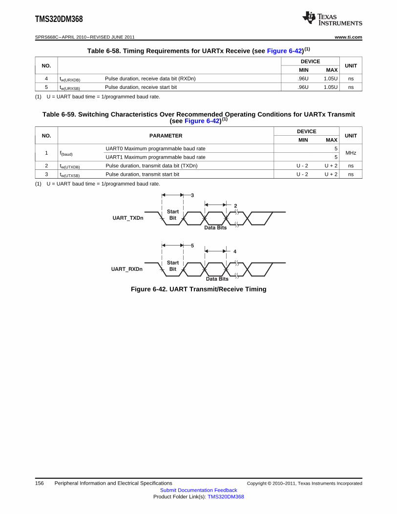
3
2Start
Bit
Data Bits
UART_TXDn
UART_RXDn
5
Data Bits
Bit
Start
4
TMS320DM368
SPRS668C–APRIL 2010–REVISED JUNE 2011 www.ti.com
Table 6-58. Timing Requirements for UARTx Receive (see Figure 6-42) (1)
DEVICENO. UNIT
MIN MAX
4 tw(URXDB) Pulse duration, receive data bit (RXDn) .96U 1.05U ns
5 tw(URXSB) Pulse duration, receive start bit .96U 1.05U ns
(1) U = UART baud time = 1/programmed baud rate.
Table 6-59. Switching Characteristics Over Recommended Operating Conditions for UARTx Transmit(see Figure 6-42) (1)
DEVICENO. PARAMETER UNIT
MIN MAX
UART0 Maximum programmable baud rate 51 f(baud) MHz
UART1 Maximum programmable baud rate 5
2 tw(UTXDB) Pulse duration, transmit data bit (TXDn) U - 2 U + 2 ns
3 tw(UTXSB) Pulse duration, transmit start bit U - 2 U + 2 ns
(1) U = UART baud time = 1/programmed baud rate.
Figure 6-42. UART Transmit/Receive Timing
156 Peripheral Information and Electrical Specifications Copyright © 2010–2011, Texas Instruments Incorporated
Submit Documentation FeedbackProduct Folder Link(s): TMS320DM368
TMS320DM368
www.ti.com SPRS668C–APRIL 2010–REVISED JUNE 2011
6.15 Serial Port Interface (SPI)
The SPI module provides a programmable length shift register which allows serial communication withother SPI devices through a 3 or 4 wire interface (Clock, Data In, Data Out, and Chip-select). The SPIsupports the following features:• Master and Slave mode operation is supported on all SPI ports (master mode means that the device
provides the serial clock)• 2 chip selects for interfacing to multiple slave SPI devices.• 3 or 4 wire interface (Clock, Data In, Data Out, and Enable)• Unique interrupt for each SPI port (except SPI4)• Separate EDMA events for SPI Receive and Transmit for each SPI port (except SPI4)• 16-bit shift register• Receive buffer register• Programmable character length (2 to 16 bits)• Programmable SPI clock frequency range• 8-bit clock prescaler• Programmable clock phase (delay or no delay)• Programmable clock polarity
Note: SPI4 slave mode does not support Chip-select input, only supports 3-wire interface.
The SPI modules do not support the following features:• GPIO mode. GPIO functionality is supported by the GIO modules for those SPI pins that are
multiplexed with GPIO signals.
6.15.1 SPI Peripheral Register Description(s)
Table 6-60 lists the SPI registers, their corresponding acronyms, and the device memory locations(offsets). These offsets apply to all device SPI modules.
Table 6-60. SPI Registers
OFFSET ACRONYM REGISTER DESCRIPTION
00h SPIGCR0 SPI global control register 0
04h SPIGCR1 SPI global control register 1
08h SPIINT SPI interrupt register
0Ch SPILVL SPI interrupt level register
10h SPIFLG SPI flag register
14h SPIPC0 SPI pin control register
18h - Reserved
1Ch SPIPC2 SPI pin control register 2
20h - 38h - Reserved
3Ch SPIDAT1 SPI shift register
40h SPIBUF SPI buffer register
44h SPIEMU SPI emulation register
48h SPIDELAY SPI delay register
4Ch SPIDEF SPI default chip select register
50h-5Ch SPIFMT0 SPI data format register 0
60h INTVECT0 SPI interrupt vector register 0
64h INTVECT1 SPI interrupt vector register 1
Copyright © 2010–2011, Texas Instruments Incorporated Peripheral Information and Electrical Specifications 157Submit Documentation Feedback
Product Folder Link(s): TMS320DM368

TMS320DM368
SPRS668C–APRIL 2010–REVISED JUNE 2011 www.ti.com
6.15.2 SPI Electrical Data/Timing
Master Mode — General
Table 6-61. General Switching Characteristics in Master Mode (1)
NO. PARAMETER MIN MAX UNIT
greater of 2P1 tc(CLK) Cycle time, SPI_SCLK 256P nsor 25
.5(tc(CLK)) -2 tw(CLKH) Pulse width, SPI_SCLK high ns1.25
.5(tc(CLK)) -3 tw(CLKL) Pulse width, SPI_SCLK low ns1.25
Output setup time, SPI_SIMO valid (1st bit) before initial SPI_SCLKrising edge, 3-/4-pin mode, 6.5polarity = 0, phase = 0
Output setup time, SPI_SIMO valid (1st bit) before initial SPI_SCLKrising edge, 3-/4-pin mode, .5tc(CLK) + 6.5polarity = 0, phase = 1
4 tosu(SIMO-CLK) nsOutput setup time, SPI_SIMO valid (1st bit) before initial SPI_SCLKfalling edge, 3-/4-pin mode, 6.5polarity = 1, phase = 0
Output setup time, SPI_SIMO valid (1st bit) before initial SPI_SCLKfalling edge, 3-/4-pin mode, .5tc(CLK) + 6.5polarity = 1, phase = 1
Delay time, SPI_SCLK transmit rising edge to SPI_SIMO output -3 6valid (subsequent bit driven), 3-/4-pin mode, polarity = 0, phase = 0
Delay time, SPI_SCLK transmit falling edge to SPI_SIMO output -3 6valid (subsequent bit driven), 3-/4-pin mode, polarity = 0, phase = 15 td(CLK-SIMO) ns
Delay time, SPI_SCLK transmit falling edge to SPI_SIMO output -3 6valid (subsequent bit driven), 3-/4-pin mode, polarity = 1, phase = 0
Delay time, SPI_SCLK transmit rising edge to SPI_SIMO output -3 6valid (subsequent bit driven), 3-/4-pin mode, polarity = 1, phase = 1
Output hold time, SPI_SIMO valid (except final bit) after receivefalling edge of SPI_SCLK, 9.53-/4-pin mode, polarity = 0, phase = 0
Output hold time, SPI_SIMO valid (except final bit) after receiverising edge of SPI_SCLK, 9.53-/4-pin mode, polarity = 0, phase = 1
6 toh(CLK-SIMO) nsOutput hold time, SPI_SIMO valid (except final bit) after receiverising edge of SPI_SCLK, 9.53-/4-pin mode, polarity = 1, phase = 0
Output hold time, SPI_SIMO valid (except final bit) after receivefalling edge of SPI_SCLK, 9.53-/4-pin mode, polarity = 1, phase = 1
(1) T = period of SPI_SCLK; For SPI0, SPI1, SPI2, and SPI3, P = period of SPI core clock (PLL1SYSCLK4). For SPI4, P = period of SPIcore clock (OSCIN).
158 Peripheral Information and Electrical Specifications Copyright © 2010–2011, Texas Instruments Incorporated
Submit Documentation FeedbackProduct Folder Link(s): TMS320DM368

TMS320DM368
www.ti.com SPRS668C–APRIL 2010–REVISED JUNE 2011
Table 6-62. General Input Timing Requirements in Master Mode
NO. MIN MAX UNIT
Setup time, SPI_SOMI valid before receive falling edge ofSPI_SCLK, 3-/4-pin mode, 4polarity = 0, phase = 0
Setup time, SPI_SOMI valid before receive rising edge ofSPI_SCLK, 3-/4-pin mode, 4polarity = 0, phase = 1
7 tsu(SOMI-CLK) nsSetup time, SPI_SOMI valid before receive rising edge ofSPI_SCLK, 3-/4-pin mode, 4polarity = 1, phase = 0
Setup time, SPI_SOMI valid before receive falling edge ofSPI_SCLK, 3-/4-pin mode, 4polarity = 1, phase = 1
Hold time, SPI_SOMI valid after receive falling edge of SPI_SCLK, 43-/4-pin mode, polarity = 0, phase = 0
Hold time, SPI_SOMI valid after receive rising edge of SPI_SCLK, 43-/4-pin mode, polarity = 0, phase = 18 th(CLK-SOMI) ns
Hold time, SPI_SOMI valid after receive rising edge of SPI_SCLK, 43-/4-pin mode, polarity = 1, phase = 0
Hold time, SPI_SOMI valid after receive falling edge of SPI_SCLK, 43-/4-pin mode, polarity = 1, phase = 1
Copyright © 2010–2011, Texas Instruments Incorporated Peripheral Information and Electrical Specifications 159Submit Documentation Feedback
Product Folder Link(s): TMS320DM368

TMS320DM368
SPRS668C–APRIL 2010–REVISED JUNE 2011 www.ti.com
Slave Mode — General
Table 6-63. General Switching Characteristics in Slave Mode (For 3-/4-Pin Modes) (1)
NO. PARAMETER MIN MAX UNIT
Delay time, transmit rising edge of SPI_SCLK to SPI_SOMI output 2 16.5valid, 3-/4-pin mode, polarity = 0, phase = 0
Delay time, transmit falling edge of SPI_SCLK to SPI_SOMI output 2 16.5valid, 3-/4-pin mode, polarity = 0, phase = 113 td(CLK-SOMI) ns
Delay time, transmit falling edge of SPI_SCLK to SPI_SOMI output 2 16.5valid, 3-/4-pin mode, polarity = 1, phase = 0
Delay time, transmit rising edge of SPI_SCLK to SPI_SOMI output 2 16.5valid, 3-/4-pin mode, polarity = 1, phase = 1
Output hold time, SPI_SOMI valid (except final bit) after receive 4falling edge of SPI_SCLK, 3-/4-pin mode, polarity = 0, phase = 0
Output hold time, SPI_SOMI valid (except final bit) after receive 4rising edge of SPI_SCLK, 3-/4-pin mode, polarity = 0, phase = 114 toh(CLK-SOMI) ns
Output hold time, SPI_SOMI valid (except final bit) after receive 4rising edge of SPI_SCLK, 3-/4-pin mode, polarity = 1, phase = 0
Output hold time, SPI_SOMI valid (except final bit) after receive 4falling edge of SPI_SCLK, 3-/4-pin mode, polarity = 1, phase = 1
(1) T = period of SPI_SCLK
160 Peripheral Information and Electrical Specifications Copyright © 2010–2011, Texas Instruments Incorporated
Submit Documentation FeedbackProduct Folder Link(s): TMS320DM368

TMS320DM368
www.ti.com SPRS668C–APRIL 2010–REVISED JUNE 2011
Table 6-64. General Input Timing Requirements in Slave Mode (1)
NO. MIN MAX UNIT
greater of 2P9 tc(CLK) Cycle time, SPI_SCLK 256P nsor 25
.5(tc(CLK)) -10 tw(CLKH) Pulse width, SPI_SCLK high ns1.25
.5(tc(CLK)) -11 tw(CLKL) Pulse width, SPI_SCLK low ns1.25
Setup time, SPI_SIMO data valid before receive falling edge ofSPI_SCLK, 3-/4-pin mode, 4polarity = 0, phase = 0
Setup time, SPI_SIMO data valid before receive rising edge ofSPI_SCLK, 3-/4-pin mode, 4polarity = 0, phase = 1
15 tsu(SIMO-CLK) nsSetup time, SPI_SIMO data valid before receive rising edge ofSPI_SCLK, 3-/4-pin mode, 4polarity = 1, phase = 0
Setup time, SPI_SIMO data valid before receive falling edge ofSPI_SCLK, 3-/4-pin mode, 4polarity = 1, phase = 1
Hold time, SPI_SIMO data valid after receive falling edge ofSPI_SCLK, 3-/4-pin mode, 4polarity = 0, phase = 0
Hold time, SPI_SIMO data valid after receive rising edge ofSPI_SCLK, 3-/4-pin mode, 4polarity = 0, phase = 1
16 th(CLK-SIMO) nsHold time, SPI_SIMO data valid after receive rising edge ofSPI_SCLK, 3-/4-pin mode, 4polarity = 1, phase = 0
Hold time, SPI_SIMO data valid after receive falling edge ofSPI_SCLK, 3-/4-pin mode, 4polarity = 1, phase = 1
(1) T = period of SPI_SCLK; For SPI0, SPI1, SPI2, and SPI3, P = period of SPI core clock (PLL1SYSCLK4). For SPI4, P = period of SPIcore clock (OSCIN).
Copyright © 2010–2011, Texas Instruments Incorporated Peripheral Information and Electrical Specifications 161Submit Documentation Feedback
Product Folder Link(s): TMS320DM368

TMS320DM368
SPRS668C–APRIL 2010–REVISED JUNE 2011 www.ti.com
Master Mode — Additional
Table 6-65. Additional Output Switching Characteristics of 4-Pin Chip-Select Option in Master Mode
NO. PARAMETER MIN MAX UNIT
Output setup time, SPI_SCS[n] active before first (C2TDELAY+2)*P+6SPI_SCLK rising edge, polarity = 0, phase = 0, .5SPIDELAY.C2TDELAY = 0
Output setup time, SPI_SCS[n] active before first (C2TDELAY+2)*PSPI_SCLK rising edge, polarity = 0, phase = 1, + .5tc + 6.5SPIDELAY.C2TDELAY = 019 tosu(CS-CLK)
(1) nsOutput setup time, SPI_SCS[n] active before first (C2TDELAY+2)*P +SPI_SCLK falling edge, polarity = 1, phase = 0, 6.5SPIDELAY.C2TDELAY = 0
Output setup time, SPI_SCS[n] active before first (C2TDELAY+2)*PSPI_SCLK falling edge, polarity = 1, phase = 1, + .5tc + 6.5SPIDELAY.C2TDELAY = 0
Delay time, final SPI_SCLK falling edge to masterdeasserting SPI_SCS[n], polarity = 0, phase = 0, (T2CDELAY+1)*P -SPIDELAY.T2CDELAY = 0, SPIDAT1.CSHOLD 3not enabled
Delay time, final SPI_SCLK falling edge to masterdeasserting SPI_SCS[n], polarity = 0, phase = 1, (T2CDELAY+1)*P -SPIDELAY.T2CDELAY = 0, SPIDAT1.CSHOLD 3not enabled
20 td(CLK-CS) nsDelay time, final SPI_SCLK rising edge to masterdeasserting SPI_SCS[n], polarity = 1, phase = 0, (T2CDELAY+1)*P -SPIDELAY.T2CDELAY = 0, SPIDAT1.CSHOLD 3not enabled
Delay time, final SPI_SCLK rising edge to masterdeasserting SPI_SCS[n], polarity = 1, phase = 1, (T2CDELAY+1)*P -SPIDELAY.T2CDELAY = 0, SPIDAT1.CSHOLD 3not enabled
(1) The Master SPI is ready with new data before SPI_SCS[n] assertion.
Slave Mode — Additional
Table 6-66. Additional Output Switching Characteristics of 4-Pin Chip-Select Option in Slave Mode (1)
NO. PARAMETER MIN MAX UNIT
Delay time, master asserting SPI_SCS[n] to slave driving27 td(CSL-SOMI) 2P + 16.5 nsSPI_SOMI data valid
Disable time, master deasserting SPI_SCS[n] to slave driving28 tdis(CSH-SOMI) 2P + 16.5 nsSPI_SOMI high impedance
(1) T = period of SPI_SCLK; For SPI0, SPI1, SPI2, and SPI3, P = period of SPI core clock (PLL1SYSCLK4). For SPI4, P = period of SPIcore clock (OSCIN).
162 Peripheral Information and Electrical Specifications Copyright © 2010–2011, Texas Instruments Incorporated
Submit Documentation FeedbackProduct Folder Link(s): TMS320DM368

TMS320DM368
www.ti.com SPRS668C–APRIL 2010–REVISED JUNE 2011
Table 6-67. Additional Input Timing Requirements of 4-Pin Chip-Select Option in Slave Mode (1)
NO. MIN MAX UNIT
Setup time, SPI_SCS[n] asserted at slave to first SPI_SCLK edge25 tsu(CSL-CLK) 2P + 25 ns(rising or falling) at slave
Delay time, final falling edge SPI_SCLK to SPI_SCS[n] .5(tc(CLK)) + 2P - 4deasserted, polarity = 0, phase = 0
Delay time, final falling edge SPI_SCLK to SPI_SCS[n] 2P - 4deasserted, polarity = 0, phase = 126 td(CLK-CSH) ns
Delay time, final rising edge SPI_SCLK to SPI_SCS[n] deasserted, .5(tc(CLK)) + 2P - 4polarity = 1, phase = 0
Delay time, final rising edge SPI_SCLK to SPI_SCS[n] deasserted, 2P - 4polarity = 1, phase = 1
(1) T = period of SPI_SCLK; For SPI0, SPI1, SPI2, and SPI3, P = period of SPI core clock (PLL1SYSCLK4). For SPI4, P = period of SPIcore clock (OSCIN).
Copyright © 2010–2011, Texas Instruments Incorporated Peripheral Information and Electrical Specifications 163Submit Documentation Feedback
Product Folder Link(s): TMS320DM368

SPI_CLK
SPI_SIMO
SPI_SOMI
SPI_CLK
SPI_SIMO
SPI_SOMI
SPI_CLK
SPI_SIMO
SPI_SOMI
SPI_CLK
SPI_SIMO
SPI_SOMI
MO(0) MO(1) MO(n-1) MO(n)
MI(0) MI(1) MI(n-1) MI(n)
MO(n)
MI(n-1)
MO(1)
6
7
7
7
7
8
8
8
8
32
6
1
4
4
4
4 5
5
5 6
MASTER MODEPOLARITY = 0 PHASE = 0
MASTER MODEPOLARITY = 0 PHASE = 1
MASTER MODEPOLARITY = 1 PHASE = 0
MASTER MODEPOLARITY = 1 PHASE = 1
5
MO(0) MO(1) MO(n-1)
MI(n)MI(n-1)MI(1)MI(0)
MO(0) MO(1) MO(n-1) MO(n)
MI(n)MI(1)MI(0)
MO(0) MO(n-1) MO(n)
MI(n)MI(n-1)MI(1)MI(0)
6
TMS320DM368
SPRS668C–APRIL 2010–REVISED JUNE 2011 www.ti.com
Figure 6-43. SPI Timings—Master Mode
164 Peripheral Information and Electrical Specifications Copyright © 2010–2011, Texas Instruments Incorporated
Submit Documentation FeedbackProduct Folder Link(s): TMS320DM368

SPI_CLK
SPI_SIMO
SPI_SOMI
SPI_CLK
SPI_SIMO
SPI_SOMI
SPI_CLK
SPI_SIMO
SPI_SOMI
SPI_CLK
SPI_SIMO
SPI_SOMI
SI(1)
SI(n-1) SI(n)
SO(0) SO(1) SO(n-1) SO(n)
SI(0) SI(1) SI(n)
SO(0) SO(1)
14
14
15
15
15
15
16
16
16
16
11
10
14
9
13
13
13
13
14
SLAVE MODEPOLARITY = 0 PHASE = 0
SLAVE MODEPOLARITY = 0 PHASE = 1
SLAVE MODEPOLARITY = 1 PHASE = 0
SLAVE MODEPOLARITY = 1 PHASE = 1
SI(1)SI(0)
SI(n-1)
SO(n-1) SO(n)
SO(n-1)
SI(n)SI(n-1)SI(1)SI(0)
SO(n)SO(1)SO(0)
SI(n)SI(n-1)
SO(n-1) SO(n)SO(1)SO(0)
SI(0)
TMS320DM368
www.ti.com SPRS668C–APRIL 2010–REVISED JUNE 2011
A. The first bit of transmit data becomes valid on the SPI_SOMI pin when software writes to the SPIDAT1 register. Formore details, see the TMS320DM36x DMSoC Serial Peripheral Interface User's Guide (literature number SPRUFH1).
Figure 6-44. SPI Timings—Slave Mode
Copyright © 2010–2011, Texas Instruments Incorporated Peripheral Information and Electrical Specifications 165Submit Documentation Feedback
Product Folder Link(s): TMS320DM368
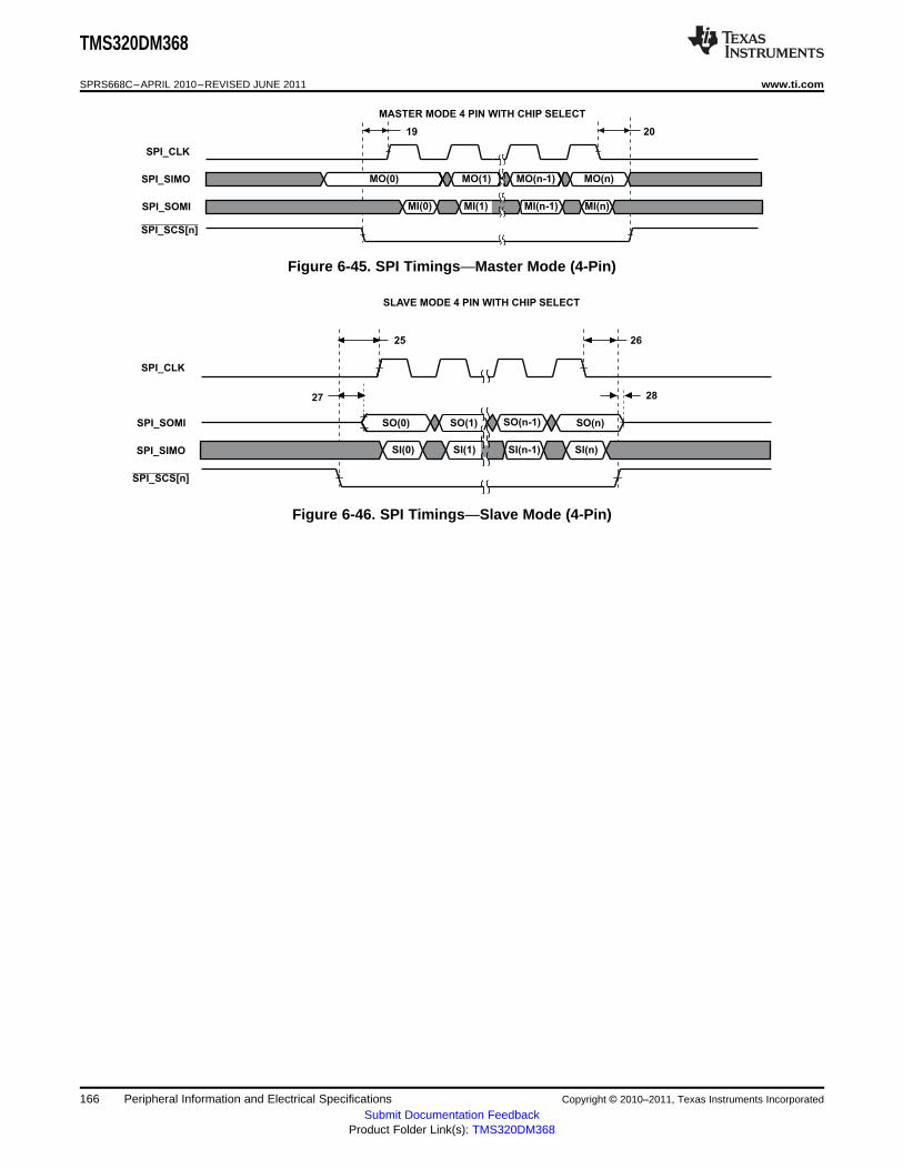
MASTER MODE 4 PIN WITH CHIP SELECT
SPI_CLK
SPI_SIMO
SPI_SOMI
SPI_SCS[n]
19 20
MO(0) MO(1) MO(n-1) MO(n)
MI(n)MI(n-1)MI(1)MI(0)
27
SPI_CLK
SPI_SOMI
SPI_SIMO
SPI_SCS[n]
SO(0)
SI(1)
26
28
25
SLAVE MODE 4 PIN WITH CHIP SELECT
SO(n)SO(n-1)
SI(0) SI(n-1) SI(n)
SO(1)
TMS320DM368
SPRS668C–APRIL 2010–REVISED JUNE 2011 www.ti.com
Figure 6-45. SPI Timings—Master Mode (4-Pin)
Figure 6-46. SPI Timings—Slave Mode (4-Pin)
166 Peripheral Information and Electrical Specifications Copyright © 2010–2011, Texas Instruments Incorporated
Submit Documentation FeedbackProduct Folder Link(s): TMS320DM368

TMS320DM368
www.ti.com SPRS668C–APRIL 2010–REVISED JUNE 2011
6.16 Inter-Integrated Circuit (I2C)
The inter-integrated circuit (I2C) module provides an interface between the DM368 and other devicescompliant with Philips Semiconductors Inter-IC bus (I2C-bus) specification version 2.1 and connected byway of an I2C-bus. External components attached to this 2-wire serial bus can transmit/receive up to 8-bitdata to/from the device through the I2C module.
The I2C port supports:• Compatible with Philips I2C Specification Revision 2.1 (January 2000)• Fast Mode up to 400 Kbps (no fail-safe I/O buffers)• Noise Filter to Remove Noise 50 ns or less• Seven- and Ten-Bit Device Addressing Modes• Master (Transmit/Receive) and Slave (Transmit/Receive) Functionality• Events: DMA, Interrupt, or Polling
For more detailed information on the I2C peripheral, see the Documentation Support section for the deviceInter-Integrated Circuit (I2C) Module Reference Guide.
6.16.1 I2C Peripheral Register Description(s)
Table 6-68 lists the I2C registers, their corresponding acronyms, and the device memory locations(offsets).
Table 6-68. Inter-Integrated Circuit (I2C) Registers
Offset Acronym Register Description
0h ICOAR I2C Own Address Register
4h ICIMR I2C Interrupt Mask Register
8h ICSTR I2C Interrupt Status Register
Ch ICCLKL I2C Clock Low-Time Divider Register
10h ICCLKH I2C Clock High-Time Divider Register
14h ICCNT I2C Data Count Register
18h ICDRR I2C Data Receive Register
1Ch ICSAR I2C Slave Address Register
20h ICDXR I2C Data Transmit Register
24h ICMDR I2C Mode Register
28h ICIVR I2C Interrupt Vector Register
2Ch ICEMDR I2C Extended Mode Register
30h ICPSC I2C Prescaler Register
34h REVID1 I2C Revision ID Register 1
38h REVID2 I2C Revision ID Register 2
48h ICPFUNC I2C Pin Function Register
4ch ICPDIR I2C Pin Direction Register
50h ICPDIN I2C Pin Data In Register
54h ICPDOUT I2C Pin Data Out Register
58h ICPDSET I2C Pin Data Set Register
5ch ICPDCLR I2C Pin Data Clear register
Copyright © 2010–2011, Texas Instruments Incorporated Peripheral Information and Electrical Specifications 167Submit Documentation Feedback
Product Folder Link(s): TMS320DM368

10
8
4
3
7
12
5
6 14
2
3
13
Stop Start RepeatedStart
Stop
SDA
SCL
1
11 9
TMS320DM368
SPRS668C–APRIL 2010–REVISED JUNE 2011 www.ti.com
6.16.2 I2C Electrical Data/Timing
6.16.2.1 Inter-Integrated Circuits (I2C) Timing
Table 6-69. Timing Requirements for I2C Timings (1) (see Figure 6-47)
DEVICE
STANDARD FASTNO. UNITMODE MODE
MIN MAX MIN MAX
1 tc(SCL) Cycle time, SCL 10 2.5 μs
2 tsu(SCLH-SDAL) Setup time, SCL high before SDA low (for a repeated START condition) 4.7 0.6 μs
Hold time, SCL low after SDA low (for a START and a repeated START3 th(SCLL-SDAL) 4 0.6 μscondition)
4 tw(SCLL) Pulse duration, SCL low 4.7 1.3 μs
5 tw(SCLH) Pulse duration, SCL high 4 0.6 μs
6 tsu(SDAV-SCLH) Setup time, SDA valid before SCL high 250 100 ns
7 th(SDA-SCLL) Hold time, SDA valid after SCL low (For I2C bus™ devices) 0 3.45 0 0.9 μs
8 tw(SDAH) Pulse duration, SDA high between STOP and START conditions 4.7 1.3 μs
20 +9 tr(SDA) Rise time, SDA 1000 0.1C 300 ns
b(1)
20 +10 tr(SCL) Rise time, SCL 1000 0.1C 300 ns
b(1)
20 +11 tf(SDA) Fall time, SDA 300 0.1C 300 ns
b(1)
20 +12 tf(SCL) Fall time, SCL 300 0.1C 300 ns
b(1)
13 tsu(SCLH-SDAH) Setup time, SCL high before SDA high (for STOP condition) 4 0.6 μs
14 tw(SP) Pulse duration, spike (must be suppressed) 50 ns
15 Cb(2) Capacitive load for each bus line 400 400 pF
(1) The I2C pins SDA and SCL do not feature fail-safe I/O buffers. These pins could potentially draw current when the device is powereddown.
(2) Cb = total capacitance of one bus line in pF. If mixed with HS-mode devices, faster fall-times are allowed.
Figure 6-47. I2C Receive Timings
168 Peripheral Information and Electrical Specifications Copyright © 2010–2011, Texas Instruments Incorporated
Submit Documentation FeedbackProduct Folder Link(s): TMS320DM368

23
19
18
22
20
21
17
18
28
Stop Start RepeatedStart
Stop
SDA
SCL
16
TMS320DM368
www.ti.com SPRS668C–APRIL 2010–REVISED JUNE 2011
Table 6-70. Switching Characteristics for I2C Timings (1) (see Figure 6-48)
DEVICE
STANDARDNO. PARAMETER FAST MODE UNITMODE
MIN MAX MIN MAX
16 tc(SCL) Cycle time, SCL 10 2.5 μs
17 td(SCLH-SDAL) Delay time, SCL high to SDA low (for a repeated START condition) 4.7 0.6 μs
Delay time, SDA low to SCL low (for a START and a repeated18 td(SDAL-SCLL) 4 0.6 μsSTART condition)
19 tw(SCLL) Pulse duration, SCL low 4.7 1.3 μs
20 tw(SCLH) Pulse duration, SCL high 4 0.6 μs
21 td(SDAV-SCLH) Delay time, SDA valid to SCL high 250 100 ns
22 tv(SCLL-SDAV) Valid time, SDA valid after SCL low (For I2C devices) 0 0 0.9 μs
23 tw(SDAH) Pulse duration, SDA high between STOP and START conditions 4.7 1.3 μs
28 td(SCLH-SDAH) Delay time, SCL high to SDA high (for STOP condition) 4 0.6 μs
29 Cp Capacitance for each I2C pin 10 10 pF
(1) Cb = total capacitance of one bus line in pF. If mixed with HS-mode devices, faster fall-times are allowed.
CAUTION
The I2C pins use a standard ±4-mA LVCMOS buffer, not the slow I/OP buffer defined inthe I2C specification. Series resistors may be necessary to reduce noise at the systemlevel.
Figure 6-48. I2C Transmit Timings
Copyright © 2010–2011, Texas Instruments Incorporated Peripheral Information and Electrical Specifications 169Submit Documentation Feedback
Product Folder Link(s): TMS320DM368

TMS320DM368
SPRS668C–APRIL 2010–REVISED JUNE 2011 www.ti.com
6.17 Multi-Channel Buffered Serial Port (McBSP)
The primary use for the Multi-Channel Buffered Serial Port (McBSP) is for audio interface purposes. Theprimary audio modes that are supported by the McBSP are the AC97 and IIS modes. In addition to theprimary audio modes, the McBSP supports general serial port receive and transmit operation, but is notintended to be used as a high-speed interface. The McBSP supports the following features:• Full-duplex communication• Double-buffered data registers, which allow a continuous data stream• Independent framing and clocking for receive and transmit• External shift clock generation or an internal programmable frequency shift clock• Double-buffered data registers, which allow a continuous data stream• Independent framing and clocking for receive and transmit• Direct interface to industry-standard codecs, analog interface chips (AICs), and other serially
connected analog-to-digital (A/D) and digital-to-analog (D/A) devices• Direct interface to AC97 compliant devices (the necessary multiphase frame synchronization capability
is provided)• Direct interface to IIS compliant devices• Direct interface to SPI protocol in master mode only• A wide selection of data sizes, including 8, 12, 16, 20, 24, and 32 bits• μ-Law and A-Law companding• 8-bit data transfers with the option of LSB or MSB first• Programmable polarity for both frame synchronization and data clocks• Highly programmable internal clock and frame generation• Direct interface to T1/E1 Framers• Multi-channel transmit and receive of up to 128 channels
For more detailed information on the McBSP peripheral, see the Documentation Support section for theMulti-Channel Buffered Serial Port (McBSP) Reference Guide.
6.17.1 McBSP Peripheral Register Description(s)
Table 6-71 lists the McBSP registers, their corresponding acronyms, and the device memory locations(offsets).
Table 6-71. McBSP Registers
Offset Acronym Register Name
- RBR (1) Receive buffer register
- RSR (1) Receive shift register
- XSR (1) Transmit shift register
00h DRR (2) (3) Data receive register
04h DXR (3) Data transmit register
08h SPCR Serial port control register
0Ch RCR Receive control register
10h XCR Transmit control register
14h SRGR Sample rate generator register
18h MCR Multichannel Control Register
Enhanced Receive Channel Enable Register1Ch RCERE0 0 Partition A/B
(1) The RBR, RSR, and XSR are not directly accessible via the CPUs or the EDMA controller.(2) The CPUs and EDMA controller can only read this register; they cannot write to it.(3) The DRR and DXR are accessible via the CPUs or the EDMA controller.
170 Peripheral Information and Electrical Specifications Copyright © 2010–2011, Texas Instruments Incorporated
Submit Documentation FeedbackProduct Folder Link(s): TMS320DM368

TMS320DM368
www.ti.com SPRS668C–APRIL 2010–REVISED JUNE 2011
Table 6-71. McBSP Registers (continued)
Offset Acronym Register Name
Enhanced Transmit Channel Enable Register20h XCERE0 0 Partition A/B
24h PCR Pin control register
Enhanced Receive Channel Enable Register28h RCERE1 1 Partition C/D
Enhanced Transmit Channel Enable Register2Ch XCERE1 1 Partition C/D
Enhanced Receive Channel Enable Register30h RCERE2 2 Partition E/F
Enhanced Transmit Channel Enable Register34h XCERE2 2 Partition E/F
Enhanced Receive Channel Enable Register38h RCERE3 3 Partition G/H
Enhanced Transmit Channel Enable Register3Ch XCERE3 3 Partition G/H
Copyright © 2010–2011, Texas Instruments Incorporated Peripheral Information and Electrical Specifications 171Submit Documentation Feedback
Product Folder Link(s): TMS320DM368

TMS320DM368
SPRS668C–APRIL 2010–REVISED JUNE 2011 www.ti.com
6.17.2 McBSP Electrical Data/Timing
6.17.2.1 Multi-Channel Buffered Serial Port (McBSP) Timing
Table 6-72. Timing Requirements for McBSP (1) (2) (see Figure 6-49)
DEVICENO. UNIT
MIN MAX
15 (3) tc(CLKS) Cycle time, CLKS CLKS ext 38.5 or 2P ns
16 (4) tw(CLKS) Pulse duration, CLKR/X high or CLKR/X low CLKS ext 19.25 or P ns
CLKR int 215 tsu(FRH-CKRL) Setup time, external FSR high before CLKR low ns
CLKR ext 6
CLKR int 06 th(CKRL-FRH) Hold time, external FSR high after CLKR low ns
CLKR ext 6
CLKR int 217 tsu(DRV-CKRL) Setup time, DR valid before CLKR low ns
CLKR ext 6
CLKR int 08 th(CKRL-DRV) Hold time, DR valid after CLKR low ns
CLKR ext 6
CLKX int 2110 tsu(FXH-CKXL) Setup time, external FSX high before CLKX low ns
CLKX ext 6
CLKX int 011 th(CKXL-FXH) Hold time, external FSX high after CLKX low ns
CLKX ext 10
(1) CLKRP = CLKXP = FSRP = FSXP = 0. If polarity of any of the signals is inverted, then the timing references of that signal are alsoinverted.
(2) P = (1/SYSCLK4), where SYSCLK4 is an output clock of PLLC1 (see Section 3.3) .(3) Use whichever value is greater. Minimum CLKR/X cycle times must be met, even when CLKR/X is generated by an internal clock
source. The minimum CLKR/X cycle times are based on internal logic speed; the maximum usable speed may be lower due to EDMAlimitations and AC timing requirements.
(4) This parameter applies to the maximum McBSP frequency. Operate serial clocks (CLKR/X) in the reasonable range of 40/60 duty cycle.
172 Peripheral Information and Electrical Specifications Copyright © 2010–2011, Texas Instruments Incorporated
Submit Documentation FeedbackProduct Folder Link(s): TMS320DM368

TMS320DM368
www.ti.com SPRS668C–APRIL 2010–REVISED JUNE 2011
Table 6-73. Switching Characteristics Over Recommended Operating Conditions for McBSP (1) (2) (3)
(see Figure 6-49)
DEVICENO. PARAMETER UNIT
MIN MAX
CLKR/X int2 (4) (5) tc(CKRX) Cycle time, CLKR/X 38.5 or 2P ns
CLKR/X ext
17 td(CLKS-CLKRX) Delay time, CLKS high to internal CLKR/X CLKR/X int 1 24
CLKR/X int 19.25 - 1 or P - 13 (6) tw(CKRX) Pulse duration, CLKR/X high or CLKR/X low ns
CLKR/X ext 19.25 or P
CLKR int -4 84 td(CKRH-FRV) Delay time, CLKR high to internal FSR valid ns
CLKR ext 3 25
CLKX int -4 89 td(CKXH-FXV) Delay time, CLKX high to internal FSX valid ns
CLKX ext 3 25
CLKX int 12 nstdis(CKXH- Disable time, DX high impedance following last data12 DXHZ) bit from CLKX high CLKX ext 25 ns
CLKX int -5 + D1 (7) 12 + D2 (7) ns13 td(CKXH-DXV) Delay time, CLKX high to DX valid
CLKX ext 3 + D1 (7) 25 + D2 (7) ns
Delay time, FSX high to DX valid FSX int 0 + D1 (8) 14 + D2 (8)
14 td(FXH-DXV) ONLY applies when in data nsFSX ext 0 + D1 (8) 25 + D2 (8)
delay 0 (XDATDLY = 00b) mode
(1) CLKRP = CLKXP = FSRP = FSXP = 0. If polarity of any of the signals is inverted, then the timing references of that signal are alsoinverted.
(2) Minimum delay times also represent minimum output hold times.(3) P = (1/SYSCLK4), where SYSCLK4 is an output clock of PLLC1 (see Section 3.3) .(4) Use whichever value is greater. Minimum CLKR/X cycle times must be met, even when CLKR/X is generated by an internal clock
source.(5) The minimum CLKR/X cycle times are based on internal logic speed; the maximum usable speed may be lower due to EDMA limitations
and AC timing requirements. Use whichever value is greater.(6) C = H or L
S = sample rate generator input clock = P if CLKSM = 1 (P = SYSCLK3 period)S = sample rate generator input clock = P_clks if CLKSM = 0 (P_clks = CLKS period)H = CLKX high pulse width = (CLKGDV/2 + 1) * S if CLKGDV is evenH = (CLKGDV + 1)/2 * S if CLKGDV is oddL = CLKX low pulse width = (CLKGDV/2) * S if CLKGDV is evenL = (CLKGDV + 1)/2 * S if CLKGDV is oddCLKGDV should be set appropriately to ensure the McBSP bit rate does not exceed the maximum limit.
(7) Extra delay from CLKX high to DX valid applies only to the first data bit of a device, if and only if DXENA = 1 in SPCR.If DXENA = 0, then D1 = D2 = 0If DXENA = 1, then D1 = 6P, D2 = 12P
(8) Extra delay from FSX high to DX valid applies only to the first data bit of a device, if and only if DXENA = 1 in SPCR.If DXENA = 0, then D1 = D2 = 0If DXENA = 1, then D1 = 6P, D2 = 12P
Copyright © 2010–2011, Texas Instruments Incorporated Peripheral Information and Electrical Specifications 173Submit Documentation Feedback
Product Folder Link(s): TMS320DM368

Bit(n-1) (n-2) (n-3)
Bit 0 Bit(n-1) (n-2) (n-3)
14
1110
9
3
3
2
8
65
44
13(A)
13(A)
A. Parameter No. 13 applies to the first data bitonly when XDATDLY ≠ 0.
CLKR
FSR (int)
FSR (ext)
DR
CLKX
FSX (int)
FSX (ext)
FSX
(XDATDLY=00b)
DX
15
CLKS
1616
17
17
32
3
7
12
TMS320DM368
SPRS668C–APRIL 2010–REVISED JUNE 2011 www.ti.com
Figure 6-49. McBSP Timing
Table 6-74. McBSP as SPI Timing RequirementsCLKSTP = 10b, CLKXP = 0 (see Figure 6-50)
MASTERNO. UNIT
MIN MAX
M30 tsu(DRV-CKXL) Setup time, DR valid before CLKX low 16 ns
M31 th(CKXL-DRV) Hold time, DR valid after CLKX low 0 ns
Table 6-75. McBSP as SPI Switching Characteristics (1) (2)
CLKSTP = 10b, CLKXP = 0 (see Figure 6-50)
MASTERNO. PARAMETER UNIT
MIN MAX
38.5 orM33 tc(CKX) Cycle time, CLKX ns2P
CLKXP - CLKXP +M24 td(CKXL-FXH) Delay time, CLKX low to FSX high (2) ns2 4
CLKXL - CLKXL +M25 td(FXL-CKXH) Delay time, FSX low to CLKX high (3) ns2 2
M26 td(CKXH-DXV) Delay time, CLKX high to DX valid -2 6 ns
CLKXL - CLKXL +M27 tdis(CKXL-DXHZ) Disable time, DX high impedance following last data bit from CLKX low ns3 8
(1) P = (1/SYSCLK4), where SYSCLK4 is an output clock of PLLC1 (see Section 3.3) .(2) T = CLKX period = (1 + CLKGDV) × 2P
L1 = CLKX low pulse width = T/2 when CLKGDV is odd or zero and = (CLKGDV/2) × 2P when CLKGDV is even.(3) FSX should be low before the rising edge of clock to enable slave devices and then begin a SPI transfer at the rising edge of the master
clock (CLKX).
174 Peripheral Information and Electrical Specifications Copyright © 2010–2011, Texas Instruments Incorporated
Submit Documentation FeedbackProduct Folder Link(s): TMS320DM368

Bit 0 Bit(n-1) (n-2) (n-3) (n-4)
Bit 0 Bit(n-1) (n-2) (n-3) (n-4)
M31M30
M26M27
M25M24
CLKX
FSX
DX
DR
M33
TMS320DM368
www.ti.com SPRS668C–APRIL 2010–REVISED JUNE 2011
Figure 6-50. McBSP as SPI: CLKSTP = 10b, CLKXP = 0
Copyright © 2010–2011, Texas Instruments Incorporated Peripheral Information and Electrical Specifications 175Submit Documentation Feedback
Product Folder Link(s): TMS320DM368

Bit 0 Bit(n-1) (n-2) (n-3) (n-4)
Bit 0 Bit(n-1) (n-2) (n-3) (n-4)
M39
M36M38M37
M35M34
CLKX
FSX
DX
DR
M40
M42
TMS320DM368
SPRS668C–APRIL 2010–REVISED JUNE 2011 www.ti.com
Table 6-76. McBSP as SPI Timing RequirementsCLKSTP = 11b, CLKXP = 0
MASTERNO. UNIT
MIN MAX
M39 tsu(DRV-CKXH) Setup time, DR valid before CLKX high 16 ns
M40 th(CKXH-DRV) Hold time, DR valid after CLKX high 1 ns
Table 6-77. McBSP as SPI Switching Characteristics (1) (2)
CLKSTP = 11b, CLKXP = 0 (see Figure 6-51)
MASTERNO. PARAMETER UNIT
MIN MAX
M42 tc(CKX) Cycle time, CLKX 38.5 or 2P ns
M34 td(CKXL-FXH) Delay time, CLKX low to FSX high (3) CLKXP - 2 CLKXP + 4 ns
M35 td(FXL-CKXH) Delay time, FSX low to CLKX high (4) CLKXP - 2 CLKXP + 2 ns
M36 td(CKXL-DXV) Delay time, CLKX low to DX valid -2 6 ns
Disable time, DX high impedance following last data bit fromM37 tdis(CKXL-DXHZ) -3 8 nsCLKX low
M38 td(FXL-DXV) Delay time, FSX low to DX valid CLKXH - 2 CLKXH + 10 ns
(1) P = (1/SYSCLK4), where SYSCLK4 is an output clock of PLLC1 (see Section 3.3).(2) T = CLKX period = (1 + CLKGDV) × 2P
L1 = CLKX low pulse width = T/2 when CLKGDV is odd or zero and = (CLKGDV/2) × 2P when CLKGDV is evenH1 = CLKX high pulse width = T/2 when CLKGDV is odd or zero and = (CLKGDV/2 + 1) × 2P when CLKGDV is even
(3) FSRP = FSXP = 1. As a SPI master, FSX is inverted to provide active-low slave-enable output.CLKXM = FSXM = 1, CLKRM = FSRM = 0 for master McBSP
(4) FSX should be low before the rising edge of clock to enable slave devices and then begin a SPI transfer at the rising edge of the masterclock (CLKX).
Figure 6-51. McBSP as SPI: CLKSTP = 11b, CLKXP = 0
176 Peripheral Information and Electrical Specifications Copyright © 2010–2011, Texas Instruments Incorporated
Submit Documentation FeedbackProduct Folder Link(s): TMS320DM368

Bit 0 Bit(n-1) (n-2) (n-3) (n-4)
Bit 0 Bit(n-1) (n-2) (n-3) (n-4)
M50M49
M45M46
M44M43
CLKX
FSX
DX
DR
M52
TMS320DM368
www.ti.com SPRS668C–APRIL 2010–REVISED JUNE 2011
Table 6-78. McBSP as SPI Timing RequirementsCLKSTP = 10b, CLKXP = 1 (see Figure 6-52)
MASTERNO. UNIT
MIN MAX
M49 tsu(DRV-CKXH) Setup time, DR valid before CLKX high 16 ns
M50 th(CKXH-DRV) Hold time, DR valid after CLKX high 0 ns
Table 6-79. McBSP as SPI Switching Characteristics (1) (2)
CLKSTP = 10b, CLKXP = 1 (see Figure 6-52)
MASTERNO. PARAMETER UNIT
MIN MAX
M52 tc(CKX) Cycle time, CLKX 38.5 or 2P ns
M43 td(CKXH-FXH) Delay time, CLKX high to FSX high (3) CLKXP - 2 CLKXP + 4 ns
M44 td(FXL-CKXL) Delay time, FSX low to CLKX low (4) CLKXH - 2 CLKXH + 2 ns
M45 td(CKXL-DXV) Delay time, CLKX low to DX valid -2 6 ns
Disable time, DX high impedance following last data bit fromM46 tdis(CKXH-DXHZ) CLKXH - 3 CLKXL + 8 nsCLKX high
(1) P = (1/SYSCLK4), where SYSCLK4 is an output clock of PLLC1 (see Section 3.3).(2) T = CLKX period = (1 + CLKGDV) × 2P
H1 = CLKX high pulse width = T/2 when CLKGDV is odd or zero and = (CLKGDV/2 + 1) × 2P when CLKGDV is even(3) FSRP = FSXP = 1. As a SPI master, FSX is inverted to provide active-low slave-enable output.
CLKXM = FSXM = 1, CLKRM = FSRM = 0 for master McBSP(4) FSX should be low before the rising edge of clock to enable slave devices and then begin a SPI transfer at the rising edge of the master
clock (CLKX).
Figure 6-52. McBSP as SPI: CLKSTP = 10b, CLKXP = 1
Copyright © 2010–2011, Texas Instruments Incorporated Peripheral Information and Electrical Specifications 177Submit Documentation Feedback
Product Folder Link(s): TMS320DM368

Bit 0 Bit(n-1) (n-2) (n-3) (n-4)
Bit 0 Bit(n-1) (n-2) (n-3) (n-4)
M59M58
M55M57M56
M54M53
CLKX
FSX
DX
DR
M62
TMS320DM368
SPRS668C–APRIL 2010–REVISED JUNE 2011 www.ti.com
Table 6-80. McBSP as SPI Timing RequirementsCLKSTP = 11b, CLKXP = 1 (see Figure 6-53)
MASTERNO. UNIT
MIN MAX
M58 tsu(DRV-CKXL) Setup time, DR valid before CLKX low 16 ns
M59 th(CKXL-DRV) Hold time, DR valid after CLKX low 0 ns
Table 6-81. McBSP as SPI Switching Characteristics (1) (2)
CLKSTP = 11b, CLKXP = 1 (see Figure 6-53)
MASTERNO. PARAMETER UNIT
MIN MAX
M62 tc(CKX) Cycle time, CLKX 38.5 or 2P ns
M53 td(CKXH-FXH) Delay time, CLKX high to FSX high (3) CLKXP - 2 CLKXP + 4 ns
M54 td(FXL-CKXL) Delay time, FSX low to CLKX low (4) CLKXP - 2 CLKXP + 2 ns
M55 td(CKXL-DXV) Delay time, CLKX high to DX valid -2 6 ns
Disable time, DX high impedance following last data bit fromM56 tdis(CKXH-DXHZ) -3 8 nsCLKX high
M57 td(FXL-DXV) Delay time, FSX low to DX valid CLKXL - 1 CLKXL + 10 ns
(1) P = (1/SYSCLK4), where SYSCLK4 is an output clock of PLLC1 (see Section 3.3).(2) T = CLKX period = (1 + CLKGDV) × 2P
L1 = CLKX low pulse width = T/2 when CLKGDV is odd or zero and = (CLKGDV/2) × 2P when CLKGDV is evenH1 = CLKX high pulse width = T/2 when CLKGDV is odd or zero and = (CLKGDV/2 + 1) × 2P when CLKGDV is even
(3) FSRP = FSXP = 1. As a SPI master, FSX is inverted to provide active-low slave-enable output.CLKXM = FSXM = 1, CLKRM = FSRM = 0 for master McBSP
(4) FSX should be low before the rising edge of clock to enable slave devices and then begin a SPI transfer at the rising edge of the masterclock (CLKX).
Figure 6-53. McBSP as SPI: CLKSTP = 11b, CLKXP = 1
178 Peripheral Information and Electrical Specifications Copyright © 2010–2011, Texas Instruments Incorporated
Submit Documentation FeedbackProduct Folder Link(s): TMS320DM368

TMS320DM368
www.ti.com SPRS668C–APRIL 2010–REVISED JUNE 2011
6.18 Timer
The device contains four software-programmable timers. Timer 0, Timer 1, Timer 3, and Timer 4(general-purpose timers) can be programmed in 64-bit mode, dual 32-bit unchained mode, or dual 32-bitchained mode. Timer 3 supports additional features over the other timers: external clock/event input,period reload, output event tied to Real Time Out (RTO) module, external event capture, and timer counterregister read reset. Timer 2 is used only as a watchdog timer. Timer 2 is tied to device reset.• 64-bit count-up counter• Timer modes:
– 64-bit general-purpose timer mode (Timer 0, 1, 3, 4)– Dual 32-bit general-purpose timer mode (Timer 0, 1, 3, 4)– Watchdog timer mode (Timer 2)
• Two possible clock sources:– Internal clock– External clock/event input via timer input pins (Timer 3)
• Three possible operation modes:– One-time operation (timer runs for one period then stops)– Continuous operation (timer automatically resets after each period)– Continuous operation with period reload (Timer 3)
• Generates interrupts to the ARM CPU• Generates sync event to EDMA• Generates output event to device reset (Timer 2)• Generates output event to Real Timer Out (RTO) module (Timer 3)• External event capture via timer input pins (Timer 3)
For more detailed information, see the TMS320DM36x DMSoC Timer/Watchdog Timer User's Guide(SPRUFH0).
6.18.1 Timer Peripheral Register Description(s)
Table 6-82 lists the Timer registers, their corresponding acronyms, and the device memory locations(offsets).
Table 6-82. Timer Global Registers
Offset Acronym Register Description
00h PID12 Peripheral Identification Register 12
04h EMUMGT Emulation Management Register
10h TIM12 Timer Counter Register 12
14h TIM34 Timer Counter Register 34
18h PRD12 Timer Period Register 12
1Ch PRD34 Timer Period Register 34
20h TCR Timer Control Register
24h TGCR Timer Global Control Register
28h WDTCR Watchdog Timer Control Register
34h REL12 Timer Reload Register 12
38h REL34 Timer Reload Register 34
3Ch CAP12 Timer Capture Register 12
40h CAP34 Timer Capture Register 34
44h INTCTL_STAT Timer Interrupt Control and Status Register
Copyright © 2010–2011, Texas Instruments Incorporated Peripheral Information and Electrical Specifications 179Submit Documentation Feedback
Product Folder Link(s): TMS320DM368

1
2
44
3
TIM_IN
TMS320DM368
SPRS668C–APRIL 2010–REVISED JUNE 2011 www.ti.com
6.18.2 Timer Electrical Data/Timing
Table 6-83. Timing Requirements for Timer Input (1) (2) (see Figure 6-54)
DEVICENO. UNIT
MIN MAX
1 tc(TIN) Cycle time, TIM_IN 4P ns
2 tw(TINPH) Pulse duration, TIM_IN high 0.45C 0.55C ns
3 tw(TINPL) Pulse duration, TIM_IN low 0.45C 0.55C ns
4 tt(TIN) Transition time, TIM_IN 5 ns
(1) GPIO001, GPIO002, GPIO003, and GPIO004 can be used as external clock inputs for Timer 3. See the TMS320DM36x DMSoCTimer/Watchdog Timer User's Guide for more information (SPRUFH0).
(2) P = MXI1/CLKIN cycle time in ns. For example, when MXI1/CLKIN frequency is 24 MHz use P = 41.6 ns.
Figure 6-54. Timer Input Timing
180 Peripheral Information and Electrical Specifications Copyright © 2010–2011, Texas Instruments Incorporated
Submit Documentation FeedbackProduct Folder Link(s): TMS320DM368

TMS320DM368
www.ti.com SPRS668C–APRIL 2010–REVISED JUNE 2011
6.19 Pulse Width Modulator (PWM)
The pulse width modulator (PWM) feature is very common in embedded systems. It provides a way togenerate a pulse periodic waveform for motor control or can act as a digital-to-analog converter with someexternal components. This PWM peripheral is basically a timer with a period counter and a first-phaseduration comparator, where bit width of the period and first-phase duration are both programmable. ThePulse Width Modulator (PWM) modules support the following features:• 32-bit period counter• 32-bit first-phase duration counter• 8-bit repeat count for one-shot operation. One-shot operation will produce N + 1 periods of the
waveform, where N is the repeat counter value.• Configurable to operate in either one-shot or continuous mode• Buffered period and first-phase duration registers• One-shot operation triggerable by hardware events with programmable edge transitions. (low-to-high or
high-to-low).• One-shot operation triggerable by the ISIF VSYNC output of the video processing subsystem (VPSS),
which allows any of the PWM instantiations to be used as a ISIF timer. This allows the device moduleto support the functions provided by the ISIF timer feature (generating strobe and shutter signals).
• One-shot operation generates N+1 periods of waveform, N being the repeat count register value• Configurable PWM output pin inactive state• Interrupt and EDMA synchronization events
6.19.1 PWM Peripheral Register Description(s)
Table 6-84 lists the PWM registers, their corresponding acronyms, and the device memory locations(offsets).
Table 6-84. Pulse Width Modulator (PWM) Registers
Offset Acronym Register Description
00h PID PWM Peripheral Identification Register
04h PCR PWM Peripheral Control Register
08h CFG PWM Configuration Register
0Ch START PWM Start Register
10h RPT PWM Repeat Count Register
14h PER PWM Period Register
18h PH1D PWM First-Phase Duration Register
6.19.2 PWM0/1/2/3 Electrical/Timing Data
Table 6-85. Switching Characteristics Over Recommended Operating Conditions for PWM0/1/2/3Outputs (1) (see Figure 6-55 and Figure 6-56)
DEVICENO. PARAMETER UNIT
MIN MAX
1 tw(PWMH) Pulse duration, PWMx high 37 ns
2 tw(PWML) Pulse duration, PWMx low 37 ns
3 tt(PWM) Transition time, PWMx 5 ns
4 td(ISIF-PWMV) Delay time, ISIF(VD) trigger event to PWMx valid 0 10 ns
(1) P = MXI1/CLKIN cycle time in ns. For example, when MXI1/CLKIN frequency is 24 MHz use P = 41.6 ns.
Copyright © 2010–2011, Texas Instruments Incorporated Peripheral Information and Electrical Specifications 181Submit Documentation Feedback
Product Folder Link(s): TMS320DM368

PWM0/1/2/3
1
3
3
2
4
VD(CCDC)
4
4
INVALID
INVALID
INVALID
VALID
VALID
VALID
PWM0
PWM1
PWM2
4
INVALID VALIDPWM3
TMS320DM368
SPRS668C–APRIL 2010–REVISED JUNE 2011 www.ti.com
Figure 6-55. PWM Output Timing
Figure 6-56. PWM Output Delay Timing
182 Peripheral Information and Electrical Specifications Copyright © 2010–2011, Texas Instruments Incorporated
Submit Documentation FeedbackProduct Folder Link(s): TMS320DM368

RTO0/1/2/3
1
3
3
2
TMS320DM368
www.ti.com SPRS668C–APRIL 2010–REVISED JUNE 2011
6.20 Real Time Out (RTO)
The device uses the Real Time Out (RTO) peripheral to provide appropriate input control signals toexternal devices such as motor controllers. This peripheral supports the following features:• Four separate outputs• Trigger on Timer3 event
6.20.1 Real Time Out (RTO) Peripheral Register Description(s)
Table 6-86 lists the RTO registers, their corresponding acronyms, and the device memory locations(offsets).
Table 6-86. Real Time Out (RTO) Registers
Offset Acronym Register Description
0h REVID RTO Controller Revision ID Register
04h CTRL_STATUS RTO Controller Control and Status Register
6.20.2 RTO Electrical/Timing Data
Table 6-87. Switching Characteristics Over Recommended Operating Conditions for RTO Outputs (seeFigure 6-57 and Figure 6-58) (1)
DEVICENO. PARAMETER UNIT
MIN MAX
52.081 tw(RTOH) Pulse duration, RTOx high 27.7 ns3
2 tw(RTOL) Pulse duration, RTOx low .45C .55C ns
3 tt(RTO) Transition time, RTOx .45C .55C ns
4 td(TIMER3-RTOV) Delay time, Timer 3 (TINT12 or TINT34) trigger event to RTOx valid 10 ns
(1) C = MXI1/CLKIN1 cycle time in ns. For example, when MXI1/CLKIN1 frequency is 24 MHz use C = 41.6 ns.
Figure 6-57. RTO Output Timing
Copyright © 2010–2011, Texas Instruments Incorporated Peripheral Information and Electrical Specifications 183Submit Documentation Feedback
Product Folder Link(s): TMS320DM368

4
TINT12/TINT34
(Timer3)
4
4
INVALID
INVALID
INVALID
VALID
VALID
VALID
RTO0
4
INVALID VALID
RTO1
RTO2
RTO3
TMS320DM368
SPRS668C–APRIL 2010–REVISED JUNE 2011 www.ti.com
Figure 6-58. RTO Output Delay Timing
184 Peripheral Information and Electrical Specifications Copyright © 2010–2011, Texas Instruments Incorporated
Submit Documentation FeedbackProduct Folder Link(s): TMS320DM368

TMS320DM368
www.ti.com SPRS668C–APRIL 2010–REVISED JUNE 2011
6.21 Ethernet Media Access Controller (EMAC)
The Ethernet Media Access Controller (EMAC) provides an efficient interface between the device and thenetwork. The EMAC supports both 10Base-T (10 Mbits/second [Mbps]) and 100Base-TX (100 Mbps) ineither half- or full-duplex mode. The EMAC module also supports hardware flow control and quality ofservice (QOS) support.
The frequencies supported for transmit and receive clocks are fixed by the IEEE 802.3 standard as:• 2.5 MHz for 10Mbps• 25 MHz for 100Mbps
The EMAC controls the flow of packet data from the device to the PHY. The MDIO module controls PHYconfiguration and status monitoring.
The EMAC module conforms to the IEEE 802.3-2002 standard, describing the “Carrier Sense MultipleAccess with Collision Detection (CSMA/CD) Access Method and Physical Layer” specifications. The IEEE802.3 standard has also been adopted by ISO/IEC and re-designated as ISO/IEC 8802-3:2000(E).
Deviation from this standard, the EMAC module does not use the Transmit Coding Error signal MTXER.Instead of driving the error pin when an underflow condition occurs on a transmitted frame, the EMAC willintentionally generate an incorrect checksum by inverting the frame CRC, so that the transmitted framewill be detected as an error by the network
Both the EMAC and the MDIO modules interface to the device through a custom interface that allowsefficient data transmission and reception. This custom interface is referred to as the EMAC controlmodule, and is considered integral to the EMAC/MDIO peripheral. The control module is also used tomultiplex and control interrupts.
For more information on the TMS320DM36x DMSoC Ethernet Media Access Controller User's Guide(literature number SPRUFI5).
6.21.1 EMAC Peripheral Register Description(s)
Table 6-88 lists the EMAC registers, their corresponding acronyms, and the device memory locations(offsets).
Table 6-88. Ethernet Media Access Controller (EMAC) Control Module Registers
Slave VBUS Acronym Register DescriptionAddress Offset
0h CMIDVER Identification and Version Register
04h CMSOFTRESET Software Reset Register
08h CMEMCONTROL Emulation Control Register
Ch CMINTCTRL Interrupt Control Register
10h CMRXTHRESHINTEN Receive Threshold Interrupt Enable Register
14h CMRXINTEN Receive Interrupt Enable Register
18h CMTXINTEN Transmit Interrupt Enable Register
1Ch CMMISCINTEN Miscellaneous Interrupt Enable Register
40h CMRXTHRESHINTSTAT Receive Threshold Interrupt Status Register
44h CMRXINTSTAT Receive Interrupt Status Register
48h CMTXINTSTAT Transmit Interrupt Status Register
4Ch CMMISCINTSTAT Miscellaneous Interrupt Status Register
70Ch CMRXINTMAX Receive Interrupts Per Millisecond Register
74h CMTXINTMAX Transmit Interrupts Per Millisecond Register
Copyright © 2010–2011, Texas Instruments Incorporated Peripheral Information and Electrical Specifications 185Submit Documentation Feedback
Product Folder Link(s): TMS320DM368

TMS320DM368
SPRS668C–APRIL 2010–REVISED JUNE 2011 www.ti.com
Table 6-89. Ethernet Media Access Controller (EMAC) Registers
Offset Acronym Register Description
0h TXIDVER Transmit Identification and Version Register
4h TXCONTROL Transmit Control Register
8h TXTEARDOWN Transmit Teardown Register
10h RXIDVER Receive Identification and Version Register
14h RXCONTROL Receive Control Register
18h RXTEARDOWN Receive Teardown Register
80h TXINTSTATRAW Transmit Interrupt Status (Unmasked) Register
84h TXINTSTATMASKED Transmit Interrupt Status (Masked) Register
88h TXINTMASKSET Transmit Interrupt Mask Set Register
8Ch TXINTMASKCLEAR Transmit Interrupt Clear Register
90h MACINVECTOR MAC Input Vector Register
94h MACEOIVECTOR MAC End of Interrupt Vector Register
A0h RXINTSTATRAW Receive Interrupt Status (Unmasked) Register
A4h RXINTSTATMASKED Receive Interrupt Status (Masked) Register
A8h RXINTMASKSET Receive Interrupt Mask Set Register
ACh RXINTMASKCLEAR Receive Interrupt Mask Clear Register
B0h MACINTSTATRAW MAC Interrupt Status (Unmasked) Register
B4h MACINTSTATMASKED MAC Interrupt Status (Masked) Register
B8h MACINTMASKSET MAC Interrupt Mask Set Register
BCh MACINTMASKCLEAR MAC Interrupt Mask Clear Register
100h RXMBPENABLE Receive Multicast/Broadcast/Promiscuous Channel Enable Register
104h RXUNICASTSET Receive Unicast Enable Set Register
108h RXUNICASTCLEAR Receive Unicast Clear Register
10Ch RXMAXLEN Receive Maximum Length Register
110h RXBUFFEROFFSET Receive Buffer Offset Register
114h RXFILTERLOWTHRESH Receive Filter Low Priority Frame Threshold Register
120h RX0FLOWTHRESH Receive Channel 0 Flow Control Threshold Register
124h RX1FLOWTHRESH Receive Channel 1 Flow Control Threshold Register
128h RX2FLOWTHRESH Receive Channel 2 Flow Control Threshold Register
12Ch RX3FLOWTHRESH Receive Channel 3 Flow Control Threshold Register
130h RX4FLOWTHRESH Receive Channel 4 Flow Control Threshold Register
134h RX5FLOWTHRESH Receive Channel 5 Flow Control Threshold Register
138h RX6FLOWTHRESH Receive Channel 6 Flow Control Threshold Register
13Ch RX7FLOWTHRESH Receive Channel 7 Flow Control Threshold Register
140h RX0FREEBUFFER Receive Channel 0 Free Buffer Count Register
144h RX1FREEBUFFER Receive Channel 1 Free Buffer Count Register
148h RX2FREEBUFFER Receive Channel 2 Free Buffer Count Register
14Ch RX3FREEBUFFER Receive Channel 3 Free Buffer Count Register
150h RX4FREEBUFFER Receive Channel 4 Free Buffer Count Register
154h RX5FREEBUFFER Receive Channel 5 Free Buffer Count Register
158h RX6FREEBUFFER Receive Channel 6 Free Buffer Count Register
15Ch RX7FREEBUFFER Receive Channel 7 Free Buffer Count Register
160h MACCONTROL MAC Control Register
164h MACSTATUS MAC Status Register
168h EMCONTROL Emulation Control Register
16Ch FIFOCONTROL FIFO Control Register
170h MACCONFIG MAC Configuration Register
186 Peripheral Information and Electrical Specifications Copyright © 2010–2011, Texas Instruments Incorporated
Submit Documentation FeedbackProduct Folder Link(s): TMS320DM368

TMS320DM368
www.ti.com SPRS668C–APRIL 2010–REVISED JUNE 2011
Table 6-89. Ethernet Media Access Controller (EMAC) Registers (continued)
Offset Acronym Register Description
174h SOFTRESET Soft Reset Register
1D0h MACSRCADDRLO MAC Source Address Low Bytes Register
1D4h MACSRCADDRHI MAC Source Address High Bytes Register
1D8h MACHASH1 MAC Hash Address Register 1
1DCh MACHASH2 MAC Hash Address Register 2
1E0h BOFFTEST Back Off Test Register
1E4h TPACETEST Transmit Pacing Algorithm Test Register
1E8h RXPAUSE Receive Pause Timer Register
1ECh TXPAUSE Transmit Pause Timer Register
500h MACADDRLO MAC Address Low Bytes Register, Used in Receive Address Matching
504h MACADDRHI MAC Address High Bytes Register, Used in Receive Address Matching
508h MACINDEX MAC Index Register
600h TX0HDP Transmit Channel 0 DMA Head Descriptor Pointer Register
604h TX1HDP Transmit Channel 1 DMA Head Descriptor Pointer Register
608h TX2HDP Transmit Channel 2 DMA Head Descriptor Pointer Register
60Ch TX3HDP Transmit Channel 3 DMA Head Descriptor Pointer Register
610h TX4HDP Transmit Channel 4 DMA Head Descriptor Pointer Register
614h TX5HDP Transmit Channel 5 DMA Head Descriptor Pointer Register
618h TX6HDP Transmit Channel 6 DMA Head Descriptor Pointer Register
61Ch TX7HDP Transmit Channel 7 DMA Head Descriptor Pointer Register
620h RX0HDP Receive Channel 0 DMA Head Descriptor Pointer Register
624h RX1HDP Receive Channel 1 DMA Head Descriptor Pointer Register
628h RX2HDP Receive Channel 2 DMA Head Descriptor Pointer Register
62Ch RX3HDP Receive Channel 3 DMA Head Descriptor Pointer Register
630h RX4HDP Receive Channel 4 DMA Head Descriptor Pointer Register
634h RX5HDP Receive Channel 5 DMA Head Descriptor Pointer Register
638h RX6HDP Receive Channel 6 DMA Head Descriptor Pointer Register
63Ch RX7HDP Receive Channel 7 DMA Head Descriptor Pointer Register
640h TX0CP Transmit Channel 0 Completion Pointer Register
644h TX1CP Transmit Channel 1 Completion Pointer Register
648h TX2CP Transmit Channel 2 Completion Pointer Register
64Ch TX3CP Transmit Channel 3 Completion Pointer Register
650h TX4CP Transmit Channel 4 Completion Pointer Register
654h TX5CP Transmit Channel 5 Completion Pointer Register
658h TX6CP Transmit Channel 6 Completion Pointer Register
65Ch TX7CP Transmit Channel 7 Completion Pointer Register
660h RX0CP Receive Channel 0 Completion Pointer Register
664h RX1CP Receive Channel 1 Completion Pointer Register
668h RX2CP Receive Channel 2 Completion Pointer Register
66Ch RX3CP Receive Channel 3 Completion Pointer Register
670h RX4CP Receive Channel 4 Completion Pointer Register
674h RX5CP Receive Channel 5 Completion Pointer Register
678h RX6CP Receive Channel 6 Completion Pointer Register
67Ch RX7CP Receive Channel 7 Completion Pointer Register
Network Statistics Registers
200h RXGOODFRAMES Good Receive Frames Register
204h RXBCASTFRAMES Broadcast Receive Frames Register
Copyright © 2010–2011, Texas Instruments Incorporated Peripheral Information and Electrical Specifications 187Submit Documentation Feedback
Product Folder Link(s): TMS320DM368

TMS320DM368
SPRS668C–APRIL 2010–REVISED JUNE 2011 www.ti.com
Table 6-89. Ethernet Media Access Controller (EMAC) Registers (continued)
Offset Acronym Register Description
208h RXMCASTFRAMES Multicast Receive Frames Register
20Ch RXPAUSEFRAMES Pause Receive Frames Register
210h RXCRCERRORS Receive CRC Errors Register
214h RXALIGNCODEERRORS Receive Alignment/Code Errors Register
218h RXOVERSIZED Receive Oversized Frames Register
21Ch RXJABBER Receive Jabber Frames Register
220h RXUNDERSIZED Receive Undersized Frames Register
224h RXFRAGMENTS Receive Frame Fragments Register
228h RXFILTERED Filtered Receive Frames Register
22Ch RXQOSFILTERED Receive QOS Filtered Frames Register
230h RXOCTETS Receive Octet Frames Register
234h TXGOODFRAMES Good Transmit Frames Register
238h TXBCASTFRAMES Broadcast Transmit Frames Register
23Ch TXMCASTFRAMES Multicast Transmit Frames Register
240h TXPAUSEFRAMES Pause Transmit Frames Register
244h TXDEFERRED Deferred Transmit Frames Register
248h TXCOLLISION Transmit Collision Frames Register
24Ch TXSINGLECOLL Transmit Single Collision Frames Register
250h TXMULTICOLL Transmit Multiple Collision Frames Register
254h TXEXCESSIVECOLL Transmit Excessive Collision Frames Register
258h TXLATECOLL Transmit Late Collision Frames Register
25Ch TXUNDERRUN Transmit Underrun Error Register
260h TXCARRIERSENSE Transmit Carrier Sense Errors Register
264h TXOCTETS Transmit Octet Frames Register
268h FRAME64 Transmit and Receive 64 Octet Frames Register
26Ch FRAME65T127 Transmit and Receive 65 to 127 Octet Frames Register
270h FRAME128T255 Transmit and Receive 128 to 255 Octet Frames Register
274h FRAME256T511 Transmit and Receive 256 to 511 Octet Frames Register
278h FRAME512T1023 Transmit and Receive 512 to 1023 Octet Frames Register
27Ch FRAME1024TUP Transmit and Receive 1024 to RXMAXLEN Octet Frames Register
280h NETOCTETS Network Octet Frames Register
284h RXSOFOVERRUNS Receive FIFO or DMA Start of Frame Overruns Register
288h RXMOFOVERRUNS Receive FIFO or DMA Middle of Frame Overruns Register
28Ch RXDMAOVERRUNS Receive DMA Overruns Register
Table 6-90. EMAC Descriptor Memory
HEX ADDRESS RANGE ACRONYM DESCRIPTION
0x01D0 8000 - 0x01D0 9FFF – EMAC Control Module Descriptor Memory
188 Peripheral Information and Electrical Specifications Copyright © 2010–2011, Texas Instruments Incorporated
Submit Documentation FeedbackProduct Folder Link(s): TMS320DM368

MRCLK
2 3
1
MTCLK
2 3
1
MRCLK (Input)
1
2
MRXD3−MRXD0,MRXDV, MRXER (Inputs)
TMS320DM368
www.ti.com SPRS668C–APRIL 2010–REVISED JUNE 2011
6.21.2 Ethernet Media Access Controller (EMAC) Electrical Data/Timing
Table 6-91. Timing Requirements for MRCLK (see Figure 6-59)
10 Mbps 100 MbpsNO. UNITMIN MAX MIN MAX
1 tc(MRCLK) Cycle time, MRCLK 400 40 ns
2 tw(MRCLKH) Pulse duration, MRCLK high 140 14 ns
3 tw(MRCLKL) Pulse duration, MRCLK low 140 14 ns
Figure 6-59. MRCLK Timing (EMAC - Receive)
Table 6-92. Timing Requirements for MTCLK (see Figure 6-59)
10 Mbps 100 MbpsNO. UNITMIN MAX MIN MAX
1 tc(MTCLK) Cycle time, MTCLK 400 40 ns
2 tw(MTCLKH) Pulse duration, MTCLK high 140 14 ns
3 tw(MTCLKL) Pulse duration, MTCLK low 140 14 ns
Figure 6-60. MTCLK Timing (EMAC - Transmit)
Table 6-93. Timing Requirements for EMAC MII Receive 10/100 Mbit/s (1) (see Figure 6-61)
NO. UNITMIN MAX
1 tsu(MRXD-MRCLKH) Setup time, receive selected signals valid before MRCLK high 8 ns
2 th(MRCLKH-MRXD) Hold time, receive selected signals valid after MRCLK high 8 ns
(1) Receive selected signals include: MRXD3-MRXD0, MRXDV, and MRXER.
Figure 6-61. EMAC Receive Interface Timing
Table 6-94. Switching Characteristics Over Recommended Operating Conditions for EMAC MII Transmit
Copyright © 2010–2011, Texas Instruments Incorporated Peripheral Information and Electrical Specifications 189Submit Documentation Feedback
Product Folder Link(s): TMS320DM368

1
MTCLK (Input)
MTXD3−MTXD0,MTXEN (Outputs)
TMS320DM368
SPRS668C–APRIL 2010–REVISED JUNE 2011 www.ti.com
Table 6-94. Switching Characteristics Over Recommended Operating Conditions for EMAC MII Transmit10/100 Mbit/s(1) (see Figure 6-62) (continued)
10/100 Mbit/s (1) (see Figure 6-62)
NO. UNITMIN MAX
1 td(MTCLKH-MTXD) Delay time, MTCLK high to transmit selected signals valid 5 25 ns
(1) Transmit selected signals include: MTXD3-MTXD0, and MTXEN.
Figure 6-62. EMAC Transmit Interface Timing
190 Peripheral Information and Electrical Specifications Copyright © 2010–2011, Texas Instruments Incorporated
Submit Documentation FeedbackProduct Folder Link(s): TMS320DM368

TMS320DM368
www.ti.com SPRS668C–APRIL 2010–REVISED JUNE 2011
6.22 Management Data Input/Output (MDIO)
The Management Data Input/Output (MDIO) module continuously polls all 32 MDIO addresses in order toenumerate all PHY devices in the system.
The Management Data Input/Output (MDIO) module implements the 802.3 serial management interface tointerrogate and control Ethernet PHY(s) using a shared two-wire bus. Host software uses the MDIOmodule to configure the auto-negotiation parameters of each PHY attached to the EMAC, retrieve thenegotiation results, and configure required parameters in the EMAC module for correct operation. Themodule is designed to allow almost transparent operation of the MDIO interface, with very littlemaintenance from the core processor. Only one PHY may be connected at any given time.
For more detailed information on the MDIO peripheral, see the TMS320DM36x DMSoC Ethernet MediaAccess Controller User's Guide (literature number SPRUFI5).
6.22.1 MDIO Peripheral Register Description(s)
Table 6-95 lists the MDIO registers, their corresponding acronyms, and the device memory locations(offsets).
Table 6-95. Management Data Input/Output (MDIO) Registers
Offset Acronym Register Description
0h VERSION Identification and Version Register
04h CONTROL MDIO Control Register
08h ALIVE PHY Alive Status register
Ch LINK PHY Link Status Register
10h LINKINTRAW MDIO Link Status Change Interrupt(Unmasked) Register
14h LINKINTMASKED MDIO Link Status Change Interrupt (Masked)Register
20h USERINTRAW MDIO User Command Complete Interrupt(Unmasked) Register
24h USERINTMASKED MDIO User Command Complete Interrupt(Masked) Register
28h USERINTMASKSET MDIO User Command Complete InterruptMask Set Register
2Ch USERINTMASKCLEAR MDIO User Command Complete InterruptMask Clear Register
80h USERACCESS0 MDIO User Access Register 0
84h USERPHYSEL0 MDIO User PHY Select Register 0
88h USERACCESS1 MDIO User Access Register 1
8Ch USERPHYSEL1 MDIO User PHY Select Register 1
6.22.2 Management Data Input/Output (MDIO) Electrical Data/Timing
Table 6-96. Timing Requirements for MDIO Input (see Figure 6-63 and Figure 6-64)
DEVICENO. UNIT
MIN MAX
1 tc(MDCLK) Cycle time, MDCLK 400 ns
2 tw(MDCLK) Pulse duration, MDCLK high/low 180 ns
3 tt(MDCLK) Transition time, MDCLK 5 ns
4 tsu(MDIO-MDCLKH) Setup time, MDIO data input valid before MDCLK high 10 ns
5 th(MDCLKH-MDIO) Hold time, MDIO data input valid after MDCLK high 0 ns
Copyright © 2010–2011, Texas Instruments Incorporated Peripheral Information and Electrical Specifications 191Submit Documentation Feedback
Product Folder Link(s): TMS320DM368

1
45
MDCLK
MDIO(input)
3 3
1
7
MDCLK
MDIO(output)
TMS320DM368
SPRS668C–APRIL 2010–REVISED JUNE 2011 www.ti.com
Figure 6-63. MDIO Input Timing
Table 6-97. Switching Characteristics Over Recommended Operating Conditions for MDIO Output(see Figure 6-64)
DEVICENO. UNIT
MIN MAX
7 td(MDCLKL-MDIO) Delay time, MDCLK low to MDIO data output valid 100 ns
Figure 6-64. MDIO Output Timing
192 Peripheral Information and Electrical Specifications Copyright © 2010–2011, Texas Instruments Incorporated
Submit Documentation FeedbackProduct Folder Link(s): TMS320DM368

TMS320DM368
www.ti.com SPRS668C–APRIL 2010–REVISED JUNE 2011
6.23 Host-Port Interface (HPI) Peripheral
Note: HPI is pin multiplexed with Asynchronous EMIF at the output pin. HPI is available only when bootmode selected is HPI boot mode. In this configuration, the device will always act as a slave.
6.23.1 HPI Device-Specific Information
The device includes a user-configurable 16-bit Host-port interface (HPI16).• Multiplexed (address/data) operation• Configurable single full-word cycle and dual half-word cycle access modes• Bursting available utilizing 8-word read and write FIFOs• HPIA register supports auto-incrementing• HPID register/FIFOs providing data-path between external host interface and system bus• Multiple strobes and control signals to allow flexible host connection• Software control of data prefetching to the HPID/FIFOs• DMSoC-to-Host interrupt output signal controlled by HPIC accesses• Host-to-DMSoC interrupt controlled by HPIC accesses
NOTE: The device HPI does not support the HAS feature. For proper HPI operation if the HAS pin isrouted out, the HAS pin must be pulled up via an external resistor.
The device HPICTL register (0x01C4 0024) is part of the System Module Registers. The HPICTL registercontrols write access to the HPI peripheral control and address registers as well as determines the hosttime-out value.
6.23.2 HPI Bus Master
The HPI peripheral includes a bus master interface that allows external device initiated transfers to accessthe DM368 system bus. See the Master Peripheral Mem Map column in Table 2-3, the device MemoryMap.
6.23.3 HPI Peripheral Register Description(s)
Table 6-98 lists the HPI registers, their corresponding acronyms, and the device memory locations(offsets).
Table 6-98. HPI Registers
Offset Acronym Register Description
0h PID Peripheral Identification Register
4h PWREMU_MGMT Power and Emulation Management Register
30h HPIC Host Port Interface Control Register
34h HPIAW Host Port Interface Write Address Register
38h HPIAR Host Port Interface Read Address Register
Copyright © 2010–2011, Texas Instruments Incorporated Peripheral Information and Electrical Specifications 193Submit Documentation Feedback
Product Folder Link(s): TMS320DM368
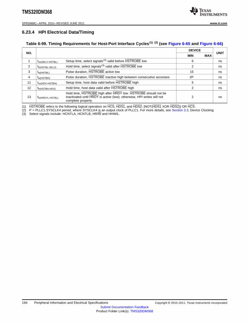
TMS320DM368
SPRS668C–APRIL 2010–REVISED JUNE 2011 www.ti.com
6.23.4 HPI Electrical Data/Timing
Table 6-99. Timing Requirements for Host-Port Interface Cycles (1) (2) (see Figure 6-65 and Figure 6-66)
DEVICENO. UNIT
MIN MAX
1 tsu(SELV-HSTBL) Setup time, select signals (3) valid before HSTROBE low 6 ns
2 th(HSTBL-SELV) Hold time, select signals (3) valid after HSTROBE low 2 ns
3 tw(HSTBL) Pulse duration, HSTROBE active low 15 ns
4 tw(HSTBH) Pulse duration, HSTROBE inactive high between consecutive accesses 2P ns
11 tsu(HDV-HSTBH) Setup time, host data valid before HSTROBE high 5 ns
12 th(HSTBH-HDV) Hold time, host data valid after HSTROBE high 2 ns
Hold time, HSTROBE high after HRDY low. HSTROBE should not be13 th(HRDYL-HSTBL) inactivated until HRDY is active (low); otherwise, HPI writes will not 2 ns
complete properly.
(1) HSTROBE refers to the following logical operation on HCS, HDS1, and HDS2: [NOT(HDS1 XOR HDS2)] OR HCS.(2) P = PLLC1.SYSCLK4 period, where SYSCLK4 is an output clock of PLLC1. For more details, see Section 3.3, Device Clocking(3) Select signals include: HCNTLA, HCNTLB, HR/W and HHWIL.
194 Peripheral Information and Electrical Specifications Copyright © 2010–2011, Texas Instruments Incorporated
Submit Documentation FeedbackProduct Folder Link(s): TMS320DM368

TMS320DM368
www.ti.com SPRS668C–APRIL 2010–REVISED JUNE 2011
Table 6-100. Switching Characteristics for Host-Port Interface Cycles (1) (2) (3)
(see Figure 6-65 and Figure 6-66)
DEVICENO. PARAMETER UNIT
MIN MAX
For HPI Write, HRDY can go high (notready) for these HPI Write conditions;otherwise, HRDY stays low (ready):Case 1: Back-to-back HPIA writes (canbe either first or second half-word)Case 2: HPIA write following aPREFETCH command (can be eitherfirst or second half-word)Case 3: HPID write when FIFO is fullor flushing (can be either first orsecond half-word)Case 4: HPIA write and Write FIFO notempty
For HPI Read, HRDY can go high (notready) for these HPI Read conditions:Case 1: HPID read (withDelay time, HSTROBE low to5 td(HSTBL-HRDYV) 17 nsauto-increment) and data not in ReadHRDY validFIFO (can only happen to firsthalf-word of HPID access)Case 2: First half-word access of HPIDRead without auto-incrementFor HPI Read, HRDY stays low (ready)for these HPI Read conditions:Case 1: HPID read with auto-incrementand data is already in Read FIFO(applies to either half-word of HPIDaccess)Case 2: HPID read withoutauto-increment and data is already inRead FIFO (always applies to secondhalf-word of HPID access)Case 3: HPIC or HPIA read (applies toeither half-word access)
6 ten(HSTBL-HDLZ) Enable time, HD driven from HSTROBE low 2 ns
7 td(HRDYL-HDV) Delay time, HRDY low to HD valid 0 ns
8 toh(HSTBH-HDV) Output hold time, HD valid after HSTROBE high 1.5 ns
14 tdis(HSTBH-HDV) Disable time, HD high-impedance from HSTROBE high 15 ns
For HPI Read. Applies to conditionswhere data is already residing inHPID/FIFO:Case 1: HPIC or HPIA readDelay time, HSTROBE low to15 td(HSTBL-HDV) Case 2: First half-word of HPID read 18 nsHD valid with auto-increment and data isalready in Read FIFOCase 3: Second half-word of HPIDread with or without auto-increment
(1) P = PLLC1.SYSCLK4 period, where SYSCLK4 is an output clock of PLLC1. For more details, see Section 3.3, Device Clocking.(2) HSTROBE refers to the following logical operation on HCS, HDS1, and HDS2: [NOT(HDS1 XOR HDS2)] OR HCS.(3) By design, whenever HCS is driven inactive (high), HPI will drive HRDY active (low).
Copyright © 2010–2011, Texas Instruments Incorporated Peripheral Information and Electrical Specifications 195Submit Documentation Feedback
Product Folder Link(s): TMS320DM368
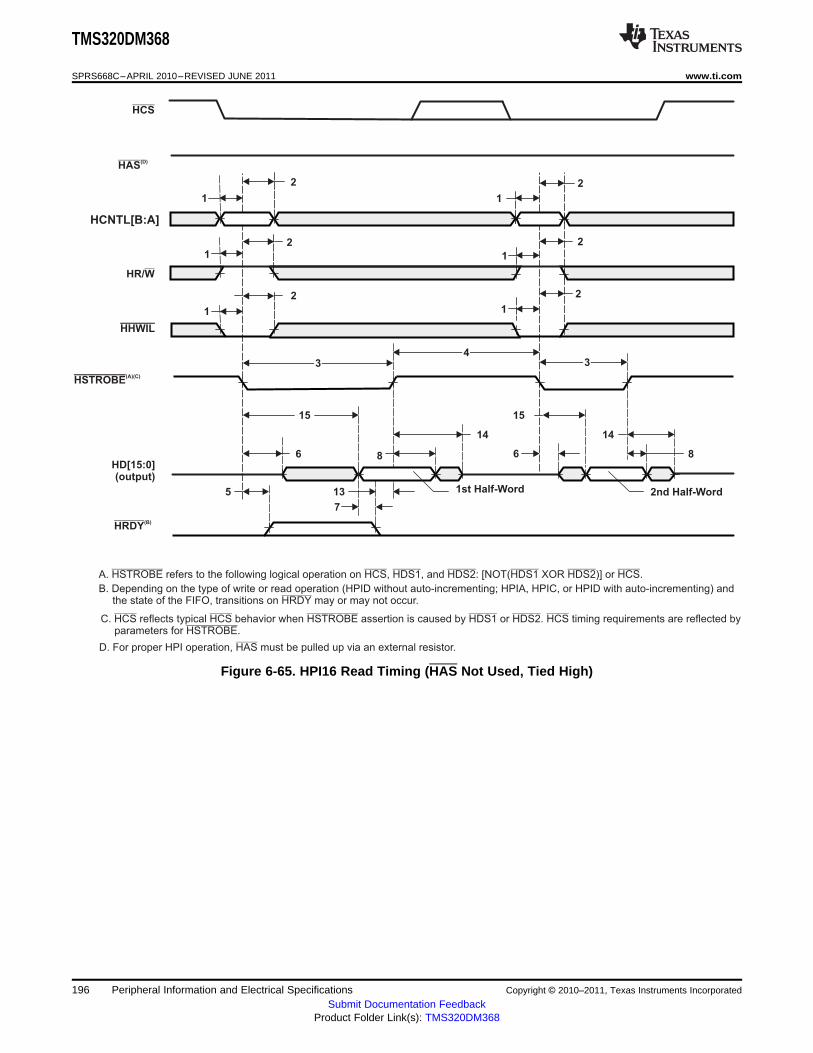
A. refers to the following logical operation on , , and : [NOT( XOR )] or .HSTROBE HCS HDS1 HDS2 HDS1 HDS2 HCS
B. Depending on the type of write or read operation (HPID without auto-incrementing; HPIA, HPIC, or HPID with auto-incrementing) andthe state of the FIFO, transitions on may or may not occur.HRDY
C. reflects typical behavior when assertion is caused by or . timing requirements are reflected byparameters for .HCS HCS HSTROBE HDS1 HDS2 HCS
HSTROBE
D. For proper HPI operation, must be pulled up via an external resistor.HAS
HCNTL[B:A]
2nd Half-Word
8
14
15
6
14
8
13
7
1st Half-Word
15
6
2
1 1
2
2
1
2
1
2
1
21
HAS(D)
HR/W
HHWIL
HSTROBE(A)(C)
HD[15:0](output)
HRDY(B)
HCS
43 3
5
TMS320DM368
SPRS668C–APRIL 2010–REVISED JUNE 2011 www.ti.com
Figure 6-65. HPI16 Read Timing (HAS Not Used, Tied High)
196 Peripheral Information and Electrical Specifications Copyright © 2010–2011, Texas Instruments Incorporated
Submit Documentation FeedbackProduct Folder Link(s): TMS320DM368
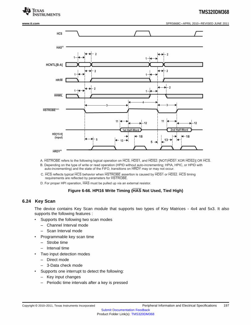
A. refers to the following logical operation on , , and : [NOT( XOR )] OR .HSTROBE HCS HDS1 HDS2 HDS1 HDS2 HCS
B. Depending on the type of write or read operation (HPID without auto-incrementing; HPIA, HPIC, or HPID withauto-incrementing) and the state of the FIFO, transitions on may or may not occur.HRDY
C. reflects typical behavior when assertion is caused by or . timingrequirements are reflected by parameters for .HCS HCS HSTROBE HDS1 HDS2 HCS
HSTROBE
D. For proper HPI operation, must be pulled up via an external resistor.HAS
HCNTL[B:A]
11
135
1
2
1
2
1
21
21
HAS(D)
HR/W
HHWIL
HSTROBE(A)(C)
HD[15:0](input)
HRDY(B)
HCS
43 3
2
1112
1st Half-Word
1318
5
2
1
2nd Half-Word
12
18
TMS320DM368
www.ti.com SPRS668C–APRIL 2010–REVISED JUNE 2011
Figure 6-66. HPI16 Write Timing (HAS Not Used, Tied High)
6.24 Key Scan
The device contains Key Scan module that supports two types of Key Matrices - 4x4 and 5x3. It alsosupports the following features :• Supports the following two scan modes
– Channel Interval mode– Scan Interval mode
• Programmable key scan time– Strobe time– Interval time
• Two input detection modes– Direct mode– 3-Data check mode
• Supports one interrupt to detect the following:– Key input changes– Periodic time intervals after a key is pressed
Copyright © 2010–2011, Texas Instruments Incorporated Peripheral Information and Electrical Specifications 197Submit Documentation Feedback
Product Folder Link(s): TMS320DM368

2
KEY_ IN[4:0]
1
KEY_OUT[3:0]
(Active Low)Hi -ZHi -Z
KEY_OUT[3:0](Always Out)
43
TMS320DM368
SPRS668C–APRIL 2010–REVISED JUNE 2011 www.ti.com
6.24.1 Key Scan Peripheral Register Description(s)
Table 6-101 lists the Key Scan registers, their corresponding acronyms, and the device memory locations(offsets).
Table 6-101. Key Scan Registers
Offset Register Description
0x0 KEYCTRL Module Control register
0x4 INTCENA Interrupt Enable control
0x8 INTFLG Interrupt Flag control
0xC INTCLR Interrupt Clear control
0x10 STRBWIDTH Strobe width
0x14 INTERVALTIME Interval Time
0x18 CONTITIME Continuous timer
0x1C CURRENTST Keyscan current status
0x20 PREVIOUSST Keyscan previous status
0x24 EMUCTRL Emulation control
6.24.2 Key Scan Electrical Data/Timing
Table 6-102. Timing Requirements for Keyscan (see Figure 6-63 and Figure 6-64)
DEVICENO UNIT. MIN MAX
(STWIDTH + 1)*CLK_P-1 (1)1 tw(KEYOUTV) Pulse duration, Keyscan out (active low mode) ns(2)
(STWIDTH + 1)*CLK_P-1 (1)2 tw(KEYOUTL) Pulse duration, Keyscan out (always out mode) ns(2)
Setup time, Keyscan input (always out mode)3 tsu(KEYOUT-KEYIN) 20 ns
Setup time, Keyscan input (active low mode)
Hold time, Keyscan input (always out mode)4 th(KEYOUT-KEYIN) 0 ns
Hold time, Keyscan input (active low mode)
(1) STWIDTH = the value programmed into the STRBWIDTH register.(2) CLK_P = 1/(PLLC1.AUXCLK/(DIV3+1)) or 1/(RTCXI), where RTCXI is the PRTCSS oscillator input pin frequency of 32.768kHz.
Figure 6-67. Key Scan Timing
198 Peripheral Information and Electrical Specifications Copyright © 2010–2011, Texas Instruments Incorporated
Submit Documentation FeedbackProduct Folder Link(s): TMS320DM368

TMS320DM368
www.ti.com SPRS668C–APRIL 2010–REVISED JUNE 2011
6.25 Analog-to-Digital Converter (ADC)
The device has a 6-channel 10-bit Analog-to-Digital Converter (ADC) interface. The analog-to-digitalconverter (ADC) feature is very common in embedded systems. The following features are supported onthe Analog-to-Digital Converter (ADC):• Six configurable analog input selects• Successive Approximation type 10 bit A-D converter• Programmable Sampling / Conversion Time (base clock is AUXCLK)• Channel select by Auto Scan conversion• Mode select by One-shot mode or Free-run mode• Programmable setup (idle) period to secure A/D sampling start time• Supports the clock stop signals to connect the PSC
For Analog-to-Digital Converter characteristics, see Section 5.2 and Section 5.3.
6.25.1 Analog-to-Digital Converter (ADC) Peripheral Register Description(s)
Table 6-103 lists the ADC registers, their corresponding acronyms, and the device memory locations(offsets).
Table 6-103. Analog-to-Digital Converter (ADC) Interface Registers
Offset Register Description
0x0 ADCTL Control register
0x4 CMPTGT Comparator target channel
0x8 CMPLDAT Comparison A/D Lower data
0xC CMPUDAT Comparison A/D Upper data
0x10 SETDIV SETUP divide value for start A/D conversion
0x14 CHSEL Analog Input channel select
0x18 AD0DAT A/D conversion data 0
0x1C AD1DAT A/D conversion data 1
0x20 AD2DAT A/D conversion data 2
0x24 AD3DAT A/D conversion data 3
0x28 AD4DAT A/D conversion data 4
0x2C AD5DAT A/D conversion data 5
0x30 EMUCTRL Emulation Control
6.26 Voice Codec
The device has Voice Codec with FIFO (Read FIFO/Write FIFO). The following features are supported onthe Voice Codec module.• 16bit x 16 word FIFO for Recording/Playback data transfer• Full differential Microphone Amplifier• Monaural single ended Line output• Monaural Speaker Amplifier (BTL)• Dynamic Range: 70dB(DAC)• Dynamic Range: 70dB(ADC)• 200-300mW Speaker output at RL = 8Ω• Sampling frequency: 8 KHz or 16 KHz• Automatic Level Control for Recording
Copyright © 2010–2011, Texas Instruments Incorporated Peripheral Information and Electrical Specifications 199Submit Documentation Feedback
Product Folder Link(s): TMS320DM368

TMS320DM368
SPRS668C–APRIL 2010–REVISED JUNE 2011 www.ti.com
• Programmable Function by Register Control– Digital Attenuator of DAC: 0 dB to -62 dB– Digital gain control for Recording (0/ +6/ +12/ +18dB)– Power Up/Down Control for each module– 20 dB/26 dB Boost Selectable for Microphone Input– Two Stage Notch filter
For Voice Codec characteristics, see Section 5.2 and Section 5.3.
6.26.1 Voice Codec Register Description(s)
Table 6-104 lists the Voice Codec registers, their corresponding acronyms, and the device memorylocations (offsets).
Table 6-104. Voice Codec Registers
Offset Register Description
0x00 VC_PID VCIF PID
0x04 VC_CTRL VCIF Control Register
0x08 VC_INTEN VCIF Interrupt enable
0x0C VC_INTSTATUS VCIF Interrupt status
0x10 VC_INTCLR VCIF Interrupt status clear
0x14 VC_EMUL_CTRL VCIF emulator Control
0x20 RFIFO VCIF Read FIFO access register
0x24 WFIFO VCIF Write FIFO access register
0x28 FIFOSTAT FIFO Status
0x80 VC_REG00 Notch filter parameter 1
0x84 VC_REG01 Notch filter parameter 1
0x88 VC_REG02 Notch filter parameter 2
0x8C VC_REG03 Notch filter parameter 2
0x90 VC_REG04 Recording side mode control
0x94 VC_REG05 PGM & MIC gain
0x98 VC_REG06 ALC
0xA4 VC_REG09 Digital soft mute/attention
0xA8 VC_REG10 Digital soft mute/attention
0xB0 VC_REG12 Power up/down control
200 Peripheral Information and Electrical Specifications Copyright © 2010–2011, Texas Instruments Incorporated
Submit Documentation FeedbackProduct Folder Link(s): TMS320DM368
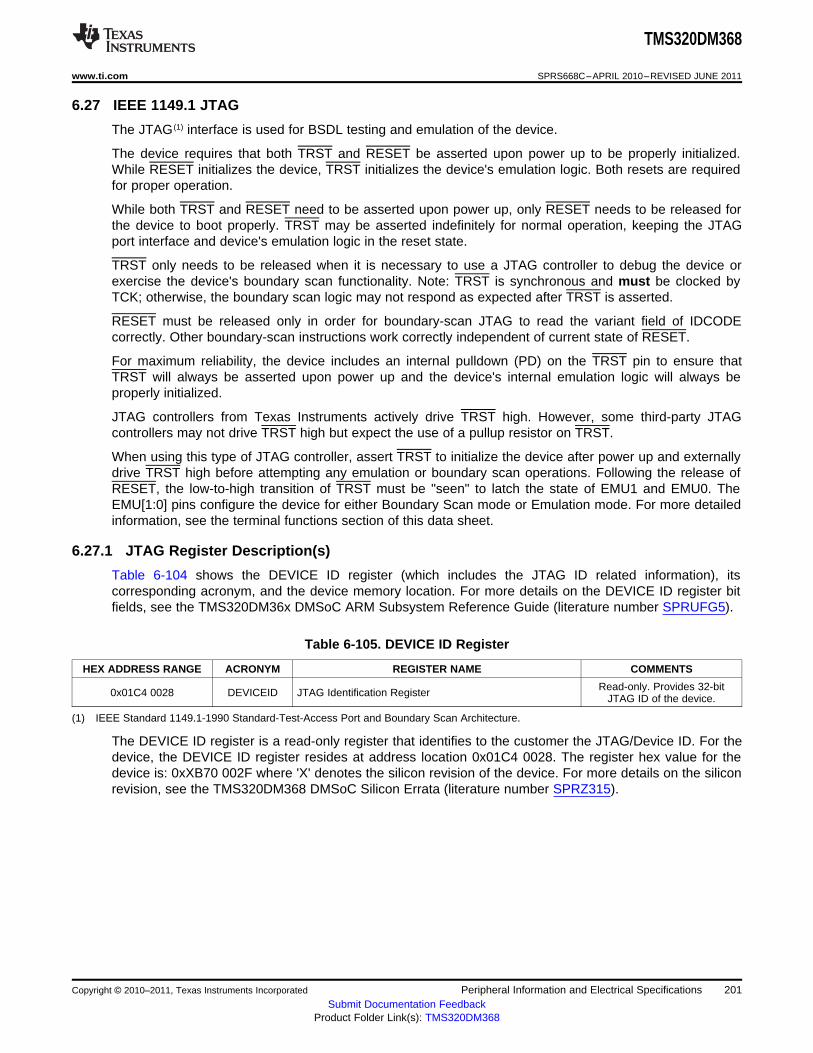
TMS320DM368
www.ti.com SPRS668C–APRIL 2010–REVISED JUNE 2011
6.27 IEEE 1149.1 JTAG
The JTAG (1) interface is used for BSDL testing and emulation of the device.
The device requires that both TRST and RESET be asserted upon power up to be properly initialized.While RESET initializes the device, TRST initializes the device's emulation logic. Both resets are requiredfor proper operation.
While both TRST and RESET need to be asserted upon power up, only RESET needs to be released forthe device to boot properly. TRST may be asserted indefinitely for normal operation, keeping the JTAGport interface and device's emulation logic in the reset state.
TRST only needs to be released when it is necessary to use a JTAG controller to debug the device orexercise the device's boundary scan functionality. Note: TRST is synchronous and must be clocked byTCK; otherwise, the boundary scan logic may not respond as expected after TRST is asserted.
RESET must be released only in order for boundary-scan JTAG to read the variant field of IDCODEcorrectly. Other boundary-scan instructions work correctly independent of current state of RESET.
For maximum reliability, the device includes an internal pulldown (PD) on the TRST pin to ensure thatTRST will always be asserted upon power up and the device's internal emulation logic will always beproperly initialized.
JTAG controllers from Texas Instruments actively drive TRST high. However, some third-party JTAGcontrollers may not drive TRST high but expect the use of a pullup resistor on TRST.
When using this type of JTAG controller, assert TRST to initialize the device after power up and externallydrive TRST high before attempting any emulation or boundary scan operations. Following the release ofRESET, the low-to-high transition of TRST must be "seen" to latch the state of EMU1 and EMU0. TheEMU[1:0] pins configure the device for either Boundary Scan mode or Emulation mode. For more detailedinformation, see the terminal functions section of this data sheet.
6.27.1 JTAG Register Description(s)
Table 6-104 shows the DEVICE ID register (which includes the JTAG ID related information), itscorresponding acronym, and the device memory location. For more details on the DEVICE ID register bitfields, see the TMS320DM36x DMSoC ARM Subsystem Reference Guide (literature number SPRUFG5).
Table 6-105. DEVICE ID Register
HEX ADDRESS RANGE ACRONYM REGISTER NAME COMMENTS
Read-only. Provides 32-bit0x01C4 0028 DEVICEID JTAG Identification Register JTAG ID of the device.
(1) IEEE Standard 1149.1-1990 Standard-Test-Access Port and Boundary Scan Architecture.
The DEVICE ID register is a read-only register that identifies to the customer the JTAG/Device ID. For thedevice, the DEVICE ID register resides at address location 0x01C4 0028. The register hex value for thedevice is: 0xXB70 002F where 'X' denotes the silicon revision of the device. For more details on the siliconrevision, see the TMS320DM368 DMSoC Silicon Errata (literature number SPRZ315).
Copyright © 2010–2011, Texas Instruments Incorporated Peripheral Information and Electrical Specifications 201Submit Documentation Feedback
Product Folder Link(s): TMS320DM368

RTCK
TDO
TDI
4
5
TMS
6
7
TCK
1
2 3
TMS320DM368
SPRS668C–APRIL 2010–REVISED JUNE 2011 www.ti.com
6.27.2 JTAG Test-Port Electrical Data/Timing
Table 6-106. Timing Requirements for JTAG Test Port (see Figure 6-68)
DEVICENO. UNIT
MIN MAX
1 tc(TCK) Cycle time, TCK 50 ns
2 tw(TCKH) Pulse duration, TCK high 20 ns
3 tw(TCKL) Pulse duration, TCK low 20 ns
4 tsu(TDIV-RTCKH) Setup time, TDI valid before RTCK high 5 ns
5 th(RTCKH-TDIIV) Hold time, TDI valid after RTCK high 10 ns
6 tsu(TMSV-RTCKH) Setup time, TMS valid before RTCK high 5 ns
7 th(RTCKH-TMSV) Hold time, TMS valid after RTCK high 10 ns
Figure 6-68. JTAG Input Timing
202 Peripheral Information and Electrical Specifications Copyright © 2010–2011, Texas Instruments Incorporated
Submit Documentation FeedbackProduct Folder Link(s): TMS320DM368

RTCK
TDO
13
8
9 10
TMS320DM368
www.ti.com SPRS668C–APRIL 2010–REVISED JUNE 2011
Table 6-107. Switching Characteristics Over Recommended Operating Conditions for JTAG Test Port(see Figure 6-68)
DEVICENO. PARAMETER UNIT
MIN MAX
8 tc(RTCK) Cycle time, RTCK 50 ns
9 tw(RTCKH) Pulse duration, RTCK high 20 ns
10 tw(RTCKL) Pulse duration, RTCK low 20 ns
11 tr(all JTAG outputs) Rise time, all JTAG outputs 5 ns
12 tf(all JTAG outputs) Fall time, all JTAG outputs 5 ns
13 td(RTCKL-TDOV) Delay time, TCK low to TDO valid 0 23 ns
Figure 6-69. JTAG Output Timing
Copyright © 2010–2011, Texas Instruments Incorporated Peripheral Information and Electrical Specifications 203Submit Documentation Feedback
Product Folder Link(s): TMS320DM368
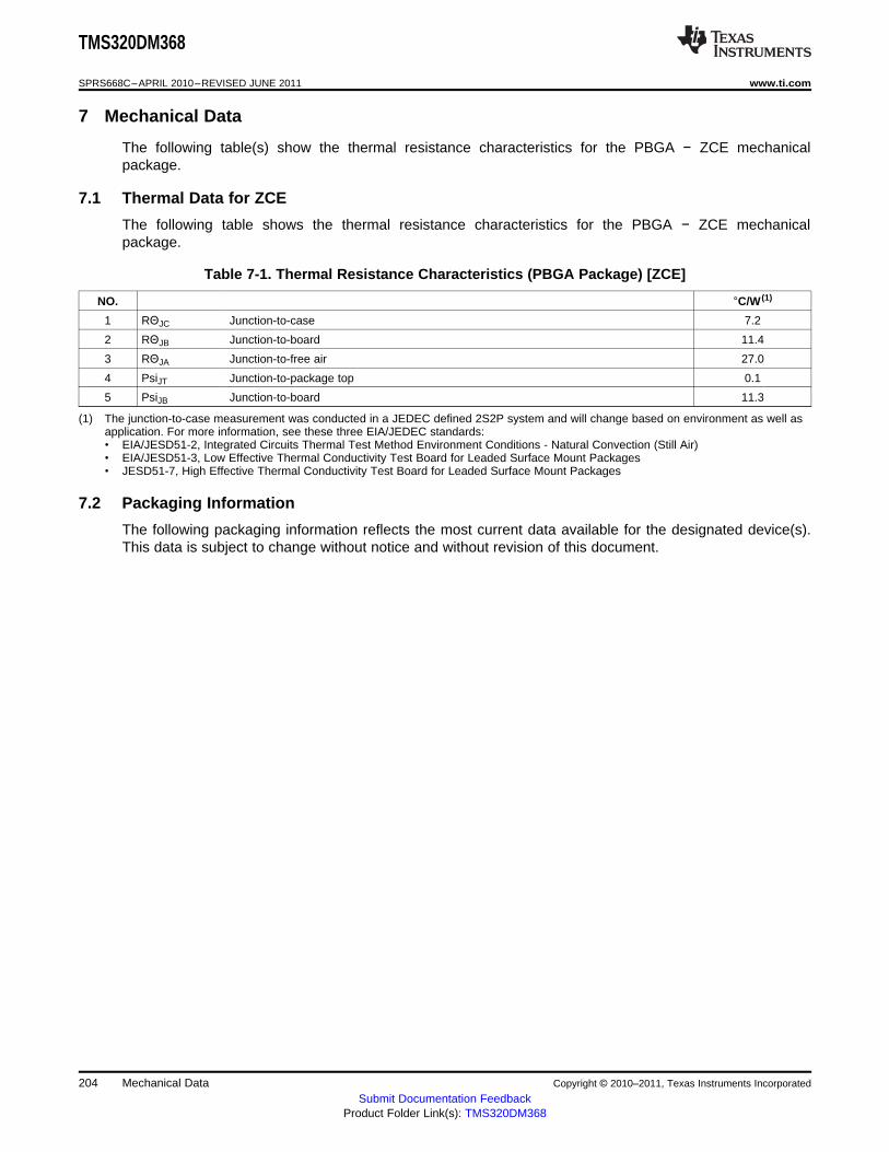
TMS320DM368
SPRS668C–APRIL 2010–REVISED JUNE 2011 www.ti.com
7 Mechanical Data
The following table(s) show the thermal resistance characteristics for the PBGA − ZCE mechanicalpackage.
7.1 Thermal Data for ZCE
The following table shows the thermal resistance characteristics for the PBGA − ZCE mechanicalpackage.
Table 7-1. Thermal Resistance Characteristics (PBGA Package) [ZCE]
NO. °C/W (1)
1 RΘJC Junction-to-case 7.2
2 RΘJB Junction-to-board 11.4
3 RΘJA Junction-to-free air 27.0
4 PsiJT Junction-to-package top 0.1
5 PsiJB Junction-to-board 11.3
(1) The junction-to-case measurement was conducted in a JEDEC defined 2S2P system and will change based on environment as well asapplication. For more information, see these three EIA/JEDEC standards:• EIA/JESD51-2, Integrated Circuits Thermal Test Method Environment Conditions - Natural Convection (Still Air)• EIA/JESD51-3, Low Effective Thermal Conductivity Test Board for Leaded Surface Mount Packages• JESD51-7, High Effective Thermal Conductivity Test Board for Leaded Surface Mount Packages
7.2 Packaging Information
The following packaging information reflects the most current data available for the designated device(s).This data is subject to change without notice and without revision of this document.
204 Mechanical Data Copyright © 2010–2011, Texas Instruments Incorporated
Submit Documentation FeedbackProduct Folder Link(s): TMS320DM368

PACKAGE OPTION ADDENDUM
www.ti.com 16-Oct-2013
Addendum-Page 1
PACKAGING INFORMATION
Orderable Device Status(1)
Package Type PackageDrawing
Pins PackageQty
Eco Plan(2)
Lead/Ball Finish MSL Peak Temp(3)
Op Temp (°C) Device Marking(4/5)
Samples
TMS320DM368ZCE ACTIVE NFBGA ZCE 338 160 Green (RoHS& no Sb/Br)
SNAGCU Level-3-260C-168 HR 0 to 85 DM368ZCE570
TMS320DM368ZCED ACTIVE NFBGA ZCE 338 160 Green (RoHS& no Sb/Br)
SNAGCU Level-3-260C-168 HR -40 to 85 DM368ZCED570
TMS320DM368ZCED48F ACTIVE NFBGA ZCE 338 160 Green (RoHS& no Sb/Br)
SNAGCU Level-3-260C-168 HR -40 to 85 DM368ZCED48F570
TMS320DM368ZCEDF ACTIVE NFBGA ZCE 338 160 Green (RoHS& no Sb/Br)
SNAGCU Level-3-260C-168 HR -40 to 85 DM368ZCEDF570
TMS320DM368ZCEF ACTIVE NFBGA ZCE 338 160 Green (RoHS& no Sb/Br)
SNAGCU Level-3-260C-168 HR 0 to 85 DM368ZCEF570
(1) The marketing status values are defined as follows:ACTIVE: Product device recommended for new designs.LIFEBUY: TI has announced that the device will be discontinued, and a lifetime-buy period is in effect.NRND: Not recommended for new designs. Device is in production to support existing customers, but TI does not recommend using this part in a new design.PREVIEW: Device has been announced but is not in production. Samples may or may not be available.OBSOLETE: TI has discontinued the production of the device.
(2) Eco Plan - The planned eco-friendly classification: Pb-Free (RoHS), Pb-Free (RoHS Exempt), or Green (RoHS & no Sb/Br) - please check http://www.ti.com/productcontent for the latest availabilityinformation and additional product content details.TBD: The Pb-Free/Green conversion plan has not been defined.Pb-Free (RoHS): TI's terms "Lead-Free" or "Pb-Free" mean semiconductor products that are compatible with the current RoHS requirements for all 6 substances, including the requirement thatlead not exceed 0.1% by weight in homogeneous materials. Where designed to be soldered at high temperatures, TI Pb-Free products are suitable for use in specified lead-free processes.Pb-Free (RoHS Exempt): This component has a RoHS exemption for either 1) lead-based flip-chip solder bumps used between the die and package, or 2) lead-based die adhesive used betweenthe die and leadframe. The component is otherwise considered Pb-Free (RoHS compatible) as defined above.Green (RoHS & no Sb/Br): TI defines "Green" to mean Pb-Free (RoHS compatible), and free of Bromine (Br) and Antimony (Sb) based flame retardants (Br or Sb do not exceed 0.1% by weightin homogeneous material)
(3) MSL, Peak Temp. -- The Moisture Sensitivity Level rating according to the JEDEC industry standard classifications, and peak solder temperature.
(4) There may be additional marking, which relates to the logo, the lot trace code information, or the environmental category on the device.
(5) Multiple Device Markings will be inside parentheses. Only one Device Marking contained in parentheses and separated by a "~" will appear on a device. If a line is indented then it is a continuationof the previous line and the two combined represent the entire Device Marking for that device.
PACKAGE OPTION ADDENDUM
www.ti.com 16-Oct-2013
Addendum-Page 2
Important Information and Disclaimer:The information provided on this page represents TI's knowledge and belief as of the date that it is provided. TI bases its knowledge and belief on informationprovided by third parties, and makes no representation or warranty as to the accuracy of such information. Efforts are underway to better integrate information from third parties. TI has taken andcontinues to take reasonable steps to provide representative and accurate information but may not have conducted destructive testing or chemical analysis on incoming materials and chemicals.TI and TI suppliers consider certain information to be proprietary, and thus CAS numbers and other limited information may not be available for release.
In no event shall TI's liability arising out of such information exceed the total purchase price of the TI part(s) at issue in this document sold by TI to Customer on an annual basis.


IMPORTANT NOTICE
Texas Instruments Incorporated and its subsidiaries (TI) reserve the right to make corrections, enhancements, improvements and otherchanges to its semiconductor products and services per JESD46, latest issue, and to discontinue any product or service per JESD48, latestissue. Buyers should obtain the latest relevant information before placing orders and should verify that such information is current andcomplete. All semiconductor products (also referred to herein as “components”) are sold subject to TI’s terms and conditions of salesupplied at the time of order acknowledgment.
TI warrants performance of its components to the specifications applicable at the time of sale, in accordance with the warranty in TI’s termsand conditions of sale of semiconductor products. Testing and other quality control techniques are used to the extent TI deems necessaryto support this warranty. Except where mandated by applicable law, testing of all parameters of each component is not necessarilyperformed.
TI assumes no liability for applications assistance or the design of Buyers’ products. Buyers are responsible for their products andapplications using TI components. To minimize the risks associated with Buyers’ products and applications, Buyers should provideadequate design and operating safeguards.
TI does not warrant or represent that any license, either express or implied, is granted under any patent right, copyright, mask work right, orother intellectual property right relating to any combination, machine, or process in which TI components or services are used. Informationpublished by TI regarding third-party products or services does not constitute a license to use such products or services or a warranty orendorsement thereof. Use of such information may require a license from a third party under the patents or other intellectual property of thethird party, or a license from TI under the patents or other intellectual property of TI.
Reproduction of significant portions of TI information in TI data books or data sheets is permissible only if reproduction is without alterationand is accompanied by all associated warranties, conditions, limitations, and notices. TI is not responsible or liable for such altereddocumentation. Information of third parties may be subject to additional restrictions.
Resale of TI components or services with statements different from or beyond the parameters stated by TI for that component or servicevoids all express and any implied warranties for the associated TI component or service and is an unfair and deceptive business practice.TI is not responsible or liable for any such statements.
Buyer acknowledges and agrees that it is solely responsible for compliance with all legal, regulatory and safety-related requirementsconcerning its products, and any use of TI components in its applications, notwithstanding any applications-related information or supportthat may be provided by TI. Buyer represents and agrees that it has all the necessary expertise to create and implement safeguards whichanticipate dangerous consequences of failures, monitor failures and their consequences, lessen the likelihood of failures that might causeharm and take appropriate remedial actions. Buyer will fully indemnify TI and its representatives against any damages arising out of the useof any TI components in safety-critical applications.
In some cases, TI components may be promoted specifically to facilitate safety-related applications. With such components, TI’s goal is tohelp enable customers to design and create their own end-product solutions that meet applicable functional safety standards andrequirements. Nonetheless, such components are subject to these terms.
No TI components are authorized for use in FDA Class III (or similar life-critical medical equipment) unless authorized officers of the partieshave executed a special agreement specifically governing such use.
Only those TI components which TI has specifically designated as military grade or “enhanced plastic” are designed and intended for use inmilitary/aerospace applications or environments. Buyer acknowledges and agrees that any military or aerospace use of TI componentswhich have not been so designated is solely at the Buyer's risk, and that Buyer is solely responsible for compliance with all legal andregulatory requirements in connection with such use.
TI has specifically designated certain components as meeting ISO/TS16949 requirements, mainly for automotive use. In any case of use ofnon-designated products, TI will not be responsible for any failure to meet ISO/TS16949.
Products Applications
Audio www.ti.com/audio Automotive and Transportation www.ti.com/automotive
Amplifiers amplifier.ti.com Communications and Telecom www.ti.com/communications
Data Converters dataconverter.ti.com Computers and Peripherals www.ti.com/computers
DLP® Products www.dlp.com Consumer Electronics www.ti.com/consumer-apps
DSP dsp.ti.com Energy and Lighting www.ti.com/energy
Clocks and Timers www.ti.com/clocks Industrial www.ti.com/industrial
Interface interface.ti.com Medical www.ti.com/medical
Logic logic.ti.com Security www.ti.com/security
Power Mgmt power.ti.com Space, Avionics and Defense www.ti.com/space-avionics-defense
Microcontrollers microcontroller.ti.com Video and Imaging www.ti.com/video
RFID www.ti-rfid.com
OMAP Applications Processors www.ti.com/omap TI E2E Community e2e.ti.com
Wireless Connectivity www.ti.com/wirelessconnectivity
Mailing Address: Texas Instruments, Post Office Box 655303, Dallas, Texas 75265Copyright © 2013, Texas Instruments Incorporated