TMS320C6713 Floating-Point Digital Signal · PDF filetms320c6713 floating-point digital signal...
115
TMS320C6713 FLOATING-POINT DIGITAL SIGNAL PROCESSOR SPRS186 – DECEMBER 2001 1 POST OFFICE BOX 1443 • HOUSTON, TEXAS 77251–1443 D Highest-Performance Floating-Point Digital Signal Processor (DSP): TMS320C6713 – Eight 32-Bit Instructions/Cycle – 32/64-Bit Data Word – 225-, 150-MHz Clock Rate – 4.4-, 6.7-ns Instruction Cycle Time – 1800 MIPS/1350 MFLOPS, 1200 MIPS /900 MFLOPS – Rich Peripheral Set, Optimized for Audio D VelociTI Advanced Very Long Instruction Word (VLIW) TMS320C67x DSP Core – Eight Independent Functional Units: – Two ALUs (Fixed-Point) – Four ALUs (Floating- and Fixed-Point) – Two Multipliers (Floating- and Fixed-Point) – Load-Store Architecture With 32 32-Bit General-Purpose Registers – Instruction Packing Reduces Code Size – All Instructions Conditional D Instruction Set Features – Native Instructions for IEEE 754 – Single- and Double-Precision – Byte-Addressable (8-, 16-, 32-Bit Data) – 8-Bit Overflow Protection – Saturation; Bit-Field Extract, Set, Clear; Bit-Counting; Normalization D L1/L2 Memory Architecture – 4K-Byte L1P Program Cache (Direct-Mapped) – 4K-Byte L1D Data Cache (2-Way) – 256K-Byte L2 Memory, With 64K-Byte L2 Unified Cache/Mapped RAM – 192K-Byte Additional L2 Mapped RAM D Device Configuration – Boot Mode: HPI, 8-, 16-, and 32-Bit ROM Boot – Endianness: Little Endian, Big Endian D 32-Bit External Memory Interface (EMIF) – Glueless Interface to SRAM, EPROM, Flash, SBSRAM, and SDRAM – 512M-Byte Total Addressable External Memory Space D Enhanced Direct-Memory-Access (EDMA) Controller (16 Independent Channels) D 16-Bit Host-Port Interface (HPI) D Two Multichannel Audio Serial Ports (McASPs) – Two Independent Clock Zones Each (1 TX and 1 RX) – Eight Serial Data Pins Per Port: Individually Assignable to any of the Clock Zones – Each Clock Zone Includes: – Programmable Clock Generator – Programmable Frame Sync Generator – TDM Streams From 2-32 Time Slots – Support for Slot Size: 8, 12, 16, 20, 24, 28, 32 Bits – Data Formatter for Bit Manipulation – Wide Variety of I2S and Similar Bit Stream Formats – Integrated Digital Audio Interface Transmitter (DIT) Supports: – S/PDIF, IEC60958-1, AES-3 Formats – Up to 16 transmit pins – Enhanced Channel Status/User Data RAM – Extensive Error Checking and Recovery D Two Inter-Integrated Circuit (I 2 C) Buses Multi-Master and Slave Interfaces D Two Multichannel Buffered Serial Ports (McBSPs): – Serial-Peripheral-Interface (SPI) – High-Speed TDM Interface – AC97 Interface D Two 32-Bit General-Purpose Timers D One Dedicated General-Purpose Input/Output Module With 16 pins D Flexible Phase-Locked-Loop (PLL) Based Clock Generator Module D IEEE-1149.1 (JTAG † ) Boundary-Scan-Compatible D Package Options: – 208-Pin PowerPAD Plastic (Low-Profile) Quad Flatpack (PYP) – 256-Pin Ball Grid Array Package (GFN) D 0.13-µm/6-Level Metal Process – CMOS Technology D 3.3-V I/Os, 1.2-V Internal PRODUCT PREVIEW Please be aware that an important notice concerning availability, standard warranty, and use in critical applications of Texas Instruments semiconductor products and disclaimers thereto appears at the end of this data sheet. PRODUCT PREVIEW information concerns products in the formative or design phase of development. Characteristic data and other specifications are design goals. Texas Instruments reserves the right to change or discontinue these products without notice. Copyright 2001, Texas Instruments Incorporated TMS320C67x, VelociTI, and PowerPAD are trademarks of Texas Instruments. All trademarks are the property of their respective owners. † IEEE Standard 1149.1-1990 Standard-Test-Access Port and Boundary Scan Architecture.
Transcript of TMS320C6713 Floating-Point Digital Signal · PDF filetms320c6713 floating-point digital signal...

TMS320C6713FLOATING-POINT DIGITAL SIGNAL PROCESSOR
SPRS186 – DECEMBER 2001
1POST OFFICE BOX 1443 • HOUSTON, TEXAS 77251–1443
Highest-Performance Floating-Point DigitalSignal Processor (DSP): TMS320C6713– Eight 32-Bit Instructions/Cycle– 32/64-Bit Data Word– 225-, 150-MHz Clock Rate– 4.4-, 6.7-ns Instruction Cycle Time– 1800 MIPS/1350 MFLOPS,
1200 MIPS /900 MFLOPS– Rich Peripheral Set, Optimized for Audio
VelociTI Advanced Very Long InstructionWord (VLIW) TMS320C67x DSP Core– Eight Independent Functional Units:
– Two ALUs (Fixed-Point)– Four ALUs (Floating- and Fixed-Point)– Two Multipliers (Floating- and
Fixed-Point)– Load-Store Architecture With 32 32-Bit
General-Purpose Registers– Instruction Packing Reduces Code Size– All Instructions Conditional
Instruction Set Features– Native Instructions for IEEE 754
– Single- and Double-Precision– Byte-Addressable (8-, 16-, 32-Bit Data)– 8-Bit Overflow Protection– Saturation; Bit-Field Extract, Set, Clear;
Bit-Counting; Normalization
L1/L2 Memory Architecture– 4K-Byte L1P Program Cache
(Direct-Mapped)– 4K-Byte L1D Data Cache (2-Way)– 256K-Byte L2 Memory, With 64K-Byte
L2 Unified Cache/Mapped RAM– 192K-Byte Additional L2 Mapped RAM
Device Configuration– Boot Mode: HPI, 8-, 16-, and 32-Bit ROM
Boot– Endianness: Little Endian, Big Endian
32-Bit External Memory Interface (EMIF)– Glueless Interface to SRAM, EPROM,
Flash, SBSRAM, and SDRAM– 512M-Byte Total Addressable External
Memory Space
Enhanced Direct-Memory-Access (EDMA)Controller (16 Independent Channels)
16-Bit Host-Port Interface (HPI)
Two Multichannel Audio Serial Ports(McASPs)– Two Independent Clock Zones Each
(1 TX and 1 RX)– Eight Serial Data Pins Per Port:
Individually Assignable to any of theClock Zones
– Each Clock Zone Includes:– Programmable Clock Generator– Programmable Frame Sync Generator– TDM Streams From 2-32 Time Slots– Support for Slot Size:
8, 12, 16, 20, 24, 28, 32 Bits– Data Formatter for Bit Manipulation
– Wide Variety of I2S and Similar BitStream Formats
– Integrated Digital Audio InterfaceTransmitter (DIT) Supports:– S/PDIF, IEC60958-1, AES-3 Formats– Up to 16 transmit pins– Enhanced Channel Status/User Data
RAM– Extensive Error Checking and Recovery
Two Inter-Integrated Circuit (I2C) BusesMulti-Master and Slave Interfaces
Two Multichannel Buffered Serial Ports(McBSPs):– Serial-Peripheral-Interface (SPI)– High-Speed TDM Interface– AC97 Interface
Two 32-Bit General-Purpose Timers
One Dedicated General-PurposeInput/Output Module With 16 pins
Flexible Phase-Locked-Loop (PLL) BasedClock Generator Module
IEEE-1149.1 (JTAG†)Boundary-Scan-Compatible
Package Options:– 208-Pin PowerPAD Plastic (Low-Profile)
Quad Flatpack (PYP)– 256-Pin Ball Grid Array Package (GFN)
0.13-µm/6-Level Metal Process– CMOS Technology
3.3-V I/Os, 1.2-V Internal
PR
OD
UC
T P
RE
VIE
W
Please be aware that an important notice concerning availability, standard warranty, and use in critical applications ofTexas Instruments semiconductor products and disclaimers thereto appears at the end of this data sheet.
PRODUCT PREVIEW information concerns products in the formative ordesign phase of development. Characteristic data and otherspecifications are design goals. Texas Instruments reserves the right tochange or discontinue these products without notice.
Copyright 2001, Texas Instruments Incorporated
TMS320C67x, VelociTI, and PowerPAD are trademarks of Texas Instruments.All trademarks are the property of their respective owners.† IEEE Standard 1149.1-1990 Standard-Test-Access Port and Boundary Scan Architecture.
TMS320C6713FLOATING-POINT DIGITAL SIGNAL PROCESSOR
SPRS186 – DECEMBER 2001
2 POST OFFICE BOX 1443 • HOUSTON, TEXAS 77251–1443
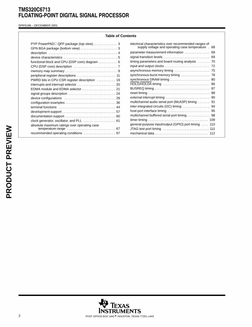
Table of Contents
electrical characteristics over recommended ranges ofsupply voltage and operating case temperature 68.
parameter measurement information 69. . . . . . . . . . . . . . . signal transition levels 69. . . . . . . . . . . . . . . . . . . . . . . . . . . . timing parameters and board routing analysis 70. . . . . . . input and output clocks 72. . . . . . . . . . . . . . . . . . . . . . . . . . . asynchronous memory timing 75. . . . . . . . . . . . . . . . . . . . . synchronous-burst memory timing 78. . . . . . . . . . . . . . . . . synchronous DRAM timing 80. . . . . . . . . . . . . . . . . . . . . . . . HOLD/HOLDA timing 86. . . . . . . . . . . . . . . . . . . . . . . . . . . . BUSREQ timing 87. . . . . . . . . . . . . . . . . . . . . . . . . . . . . . . . . reset timing 88. . . . . . . . . . . . . . . . . . . . . . . . . . . . . . . . . . . . . external interrupt timing 90. . . . . . . . . . . . . . . . . . . . . . . . . . multichannel audio serial port (McASP) timing 91. . . . . . . inter-integrated circuits (I2C) timing 94. . . . . . . . . . . . . . . . host-port interface timing 95. . . . . . . . . . . . . . . . . . . . . . . . . multichannel buffered serial port timing 98. . . . . . . . . . . . . timer timing 109. . . . . . . . . . . . . . . . . . . . . . . . . . . . . . . . . . . . general-purpose input/output (GPIO) port timing 110. . . . JTAG test-port timing 111. . . . . . . . . . . . . . . . . . . . . . . . . . . . mechanical data 112. . . . . . . . . . . . . . . . . . . . . . . . . . . . . . . .
PYP PowerPAD QFP package (top view) 3. . . . . . . . . . . . . . GFN BGA package (bottom view) 3. . . . . . . . . . . . . . . . . . . . . . description 4. . . . . . . . . . . . . . . . . . . . . . . . . . . . . . . . . . . . . . . . . device characteristics 5. . . . . . . . . . . . . . . . . . . . . . . . . . . . . . . . functional block and CPU (DSP core) diagram 6. . . . . . . . . . . CPU (DSP core) description 7. . . . . . . . . . . . . . . . . . . . . . . . . . memory map summary 9. . . . . . . . . . . . . . . . . . . . . . . . . . . . . . . peripheral register descriptions 11. . . . . . . . . . . . . . . . . . . . . . . PWRD bits in CPU CSR register description 19. . . . . . . . . . . interrupts and interrupt selector 20. . . . . . . . . . . . . . . . . . . . . . . EDMA module and EDMA selector 21. . . . . . . . . . . . . . . . . . . . signal groups description 24. . . . . . . . . . . . . . . . . . . . . . . . . . . . device configurations 29. . . . . . . . . . . . . . . . . . . . . . . . . . . . . . . configuration examples 36. . . . . . . . . . . . . . . . . . . . . . . . . . . . . . terminal functions 44. . . . . . . . . . . . . . . . . . . . . . . . . . . . . . . . . . development support 57. . . . . . . . . . . . . . . . . . . . . . . . . . . . . . . . documentation support 60. . . . . . . . . . . . . . . . . . . . . . . . . . . . . . clock generator, oscillator, and PLL 61. . . . . . . . . . . . . . . . . . . absolute maximum ratings over operating case
temperature range 67. . . . . . . . . . . . . . . . . . . . . . . . . . . . . recommended operating conditions 67. . . . . . . . . . . . . . . . . . .
PR
OD
UC
T P
RE
VIE
W

TMS320C6713FLOATING-POINT DIGITAL SIGNAL PROCESSOR
SPRS186 – DECEMBER 2001
3POST OFFICE BOX 1443 • HOUSTON, TEXAS 77251–1443
PYP PowerPAD QFP package (top view)
PYP 208-PIN PowerPAD PLASTIC QUAD FLATPACK (PQFP)(TOP VIEW)
105
104
53
52
157
208
156
1
GFN BGA package (bottom view)
1915 1713119
Y
V
TU
PN
R
W
75
L
JK
H
FG
31
D
BC
A
E
M
2 4 6 8 201816141210
GFN 256-PIN BALL GRID ARRAY (BGA) PACKAGE(BOTTOM VIEW)
PR
OD
UC
T P
RE
VIE
W

TMS320C6713FLOATING-POINT DIGITAL SIGNAL PROCESSOR
SPRS186 – DECEMBER 2001
4 POST OFFICE BOX 1443 • HOUSTON, TEXAS 77251–1443
description
The TMS320C67x DSPs (including the TMS320C6713 device) compose the floating–point DSP generationin the TMS320C6000 DSP platform. The TMS320C6713 (C6713) device is based on the high-performance,advanced VelociTI very-long-instruction-word (VLIW) architecture developed by Texas Instruments (TI),making this DSP an excellent choice for multichannel and multifunction applications.
Operating at 225 MHz, the C6713 delivers up to 1350 million floating-point operations per second (MFLOPS),1800 million instructions per second (MIPS), and with dual fixed-/floating-point multipliers up to 450 millionmultiply-accumulate operations per second (MMACS).
The C6713 uses a two-level cache-based architecture and has a powerful and diverse set of peripherals. TheLevel 1 program cache (L1P) is a 4K-Byte direct-mapped cache and the Level 1 data cache (L1D) is a 4K-Byte2-way set-associative cache. The Level 2 memory/cache (L2) consists of a 256K-Byte memory space that isshared between program and data space. 64K Bytes of the 256K Bytes in L2 memory can be configured asmapped memory, cache, or combinations of the two. The remaining 192K Bytes in L2 serves as mapped SRAM.
The C6713 has a rich peripheral set that includes two Multichannel Audio Serial Ports (McASPs), twoMultichannel Buffered Serial Ports (McBSPs), two Inter-Integrated Circuit (I2C) buses, one dedicatedGeneral-Purpose Input/Output (GPIO) module, two general-purpose timers, a host-port interface (HPI), and aglueless external memory interface (EMIF) capable of interfacing to SDRAM, SBSRAM, and asynchronousperipherals.
The two McASP interface modules each support one transmit and one receive clock zone. Each of the McASPhas eight serial data pins which can be individually allocated to any of the two zones. The serial port supportstime-division multiplexing on each pin from 2 to 32 time slots. The C6713 has sufficient bandwidth to supportall 16 serial data pins transmitting a 192 kHz stereo signal. Serial data in each zone may be transmitted andreceived on multiple serial data pins simultaneously and formatted in a multitude of variations on the PhilipsInter-IC Sound (I2S) format.
In addition, the McASP transmitter may be programmed to output multiple S/PDIF, IEC60958, AES-3 encodeddata channels simultaneously, with a single RAM containing the full implementation of user data and channelstatus fields.
The McASP also provides extensive error-checking and recovery features, such as the bad clock detectioncircuit for each high-frequency master clock which verifies that the master clock is within a programmedfrequency range.
The two I2C ports on the TMS320C6713 allow the DSP to easily control peripheral devices, boot from a serialEEPROM, and communicate with a host processor.
The TMS320C67x DSP generation is supported by the TI eXpressDSP set of industry benchmarkdevelopment tools, including a highly optimizing C/C++ Compiler, the Code Composer Studio IntegratedDevelopment Environment (IDE), JTAG-based emulation and real-time debugging, and the DSP/BIOSkernel.
PR
OD
UC
T P
RE
VIE
W
TMS320C6000, eXpressDSP, Code Composer Studio, and DSP/BIOS are trademarks of Texas Instruments.

TMS320C6713FLOATING-POINT DIGITAL SIGNAL PROCESSOR
SPRS186 – DECEMBER 2001
5POST OFFICE BOX 1443 • HOUSTON, TEXAS 77251–1443
device characteristics
Table 1 provides an overview of the C6713 DSP. The table shows significant features of the C6713 device,including the capacity of on-chip RAM, the peripherals, the execution time, and the package type with pin count.For more details on the C67x DSP device part numbers and part numbering, see Table 32 and Figure 11.
Table 1. Characteristics of the C6713 Processor
HARDWARE FEATURES
C6713(FLOATING-POINT DSP)HARDWARE FEATURES
GFN PYP
EMIF 1 (32 bit) 1 (16 bit)
EDMA (16 Channels) 1
HPI (16 bit) 1
PeripheralsMcASPs 2
PeripheralsI2Cs 2
McBSPs 2
32-Bit Timers 2
GPIO Modules 1
Size (Bytes) 264K
On-Chip MemoryOrganization
4K-Byte (4KB) L1 Program (L1P) Cache4KB L1 Data (L1D) Cache64KB Unified L2 Cache/Mapped RAM192KB L2 Mapped RAM
CPU ID+CPU Rev IDControl Status Register(CSR.[31:16])
0x0203
Frequency MHz 225, 150 150
Cycle Time ns4.4 ns (C6713GFN-225), 6.7 ns (C6713GFN-150)
6.7 ns (C6713PYP-150)
VoltageCore (V) 1.2
VoltageI/O (V) 3.3
Clock Generator OptionsPrescalerMultiplierPostscaler
/1, /2, /3, ..., /32x1, x2, x3, ..., x16/1, /2, /3, ..., /32
27 x 27 mm 256-Pin BGA (GFN) –
Packages28 x 28 mm –
208-Pin PowerPAD PQFP(PYP)
Process Technology µm 0.13
Product StatusProduct Preview (PP)Advance Information (AI)Production Data (PD)
PP PP
PR
OD
UC
T P
RE
VIE
W
C67x is a trademark of Texas Instruments.

TMS320C6713FLOATING-POINT DIGITAL SIGNAL PROCESSOR
SPRS186 – DECEMBER 2001
6 POST OFFICE BOX 1443 • HOUSTON, TEXAS 77251–1443
functional block and CPU (DSP core) diagram
Test
C67x CPU
Data Path B
B Register File
Instruction Fetch
Instruction Dispatch
Instruction Decode
Data Path A
A Register File
Power-DownLogic
.L1† .S1† .M1† .D1 .D2 .M2† .S2† .L2†
L1P CacheDirect Mapped4K Bytes Total
ControlRegisters
ControlLogic
L1D Cache2-Way
Set Associative4K Bytes
In-CircuitEmulation
InterruptControl
C6713 Digital Signal Processor
† In addition to fixed-point instructions, these functional units execute floating-point instructions.
EnhancedDMA
Controller(16 channel)
L2 Cache/Memory4 Banks
64K BytesTotal
(up to4-Way)
Clock Generator,Oscillator, and PLL
x1 through x16Multipliers
L2Memory
192KBytes
EMIF
McASP1
McASP0
McBSP1
McBSP0
I2C1
I2C0
Timer 1
Timer 0
GPIO
HPI
Pin
Mu
ltip
lexi
ng
McBSPs interface to:–SPI Control Port–High-Speed TDM Codecs–AC97 Codecs–Serial EEPROM
EMIF interfaces to: –SDRAM–SBSRAM–SRAM, –ROM/Flash, and –I/O devices
McASPs interface to:–I2S Multichannel ADC, DAC, Codec, DIR–DIT: Multiple Outputs
32
16PR
OD
UC
T P
RE
VIE
W

TMS320C6713FLOATING-POINT DIGITAL SIGNAL PROCESSOR
SPRS186 – DECEMBER 2001
7POST OFFICE BOX 1443 • HOUSTON, TEXAS 77251–1443
CPU (DSP core) description
The TMS320C6713 floating-point digital signal processor is based on the C67x CPU. The CPU fetchesVelociTI advanced very-long instruction words (VLIW) (256 bits wide) to supply up to eight 32-bit instructionsto the eight functional units during every clock cycle. The VelociTI VLIW architecture features controls bywhich all eight units do not have to be supplied with instructions if they are not ready to execute. The first bitof every 32-bit instruction determines if the next instruction belongs to the same execute packet as the previousinstruction, or whether it should be executed in the following clock as a part of the next execute packet. Fetchpackets are always 256 bits wide; however, the execute packets can vary in size. The variable-length executepackets are a key memory-saving feature, distinguishing the C67x CPU from other VLIW architectures.
The CPU features two sets of functional units. Each set contains four units and a register file. One set containsfunctional units .L1, .S1, .M1, and .D1; the other set contains units .D2, .M2, .S2, and .L2. The two register fileseach contain 16 32-bit registers for a total of 32 general-purpose registers. The two sets of functional units, alongwith two register files, compose sides A and B of the CPU (see the functional block and CPU diagram andFigure 1). The four functional units on each side of the CPU can freely share the 16 registers belonging to thatside. Additionally, each side features a single data bus connected to all the registers on the other side, by whichthe two sets of functional units can access data from the register files on the opposite side. While register accessby functional units on the same side of the CPU as the register file can service all the units in a single clock cycle,register access using the register file across the CPU supports one read and one write per cycle.
The C67x CPU executes all C62x instructions. In addition to C62x fixed-point instructions, the six out of eightfunctional units (.L1, .S1, .M1, .M2, .S2, and .L2) also execute floating-point instructions. The remaining twofunctional units (.D1 and .D2) also execute the new LDDW instruction which loads 64 bits per CPU side for atotal of 128 bits per cycle.
Another key feature of the C67x CPU is the load/store architecture, where all instructions operate on registers(as opposed to data in memory). Two sets of data-addressing units (.D1 and .D2) are responsible for all datatransfers between the register files and the memory. The data address driven by the .D units allows dataaddresses generated from one register file to be used to load or store data to or from the other register file. TheC67x CPU supports a variety of indirect addressing modes using either linear- or circular-addressing modeswith 5- or 15-bit offsets. All instructions are conditional, and most can access any one of the 32 registers. Someregisters, however, are singled out to support specific addressing or to hold the condition for conditionalinstructions (if the condition is not automatically “true”). The two .M functional units are dedicated for multiplies.The two .S and .L functional units perform a general set of arithmetic, logical, and branch functions with resultsavailable every clock cycle.
The processing flow begins when a 256-bit-wide instruction fetch packet is fetched from a program memory.The 32-bit instructions destined for the individual functional units are “linked” together by “1” bits in the leastsignificant bit (LSB) position of the instructions. The instructions that are “chained” together for simultaneousexecution (up to eight in total) compose an execute packet. A “0” in the LSB of an instruction breaks the chain,effectively placing the instructions that follow it in the next execute packet. If an execute packet crosses thefetch-packet boundary (256 bits wide), the assembler places it in the next fetch packet, while the remainder ofthe current fetch packet is padded with NOP instructions. The number of execute packets within a fetch packetcan vary from one to eight. Execute packets are dispatched to their respective functional units at the rate of oneper clock cycle and the next 256-bit fetch packet is not fetched until all the execute packets from the current fetchpacket have been dispatched. After decoding, the instructions simultaneously drive all active functional unitsfor a maximum execution rate of eight instructions every clock cycle. While most results are stored in 32-bitregisters, they can be subsequently moved to memory as bytes or half-words as well. All load and storeinstructions are byte-, half-word, or word-addressable.
PR
OD
UC
T P
RE
VIE
W

TMS320C6713FLOATING-POINT DIGITAL SIGNAL PROCESSOR
SPRS186 – DECEMBER 2001
8 POST OFFICE BOX 1443 • HOUSTON, TEXAS 77251–1443
CPU (DSP core) description (continued)
8
ÁÁÁÁÁÁÁÁÁÁÁÁÁÁÁÁÁÁÁÁ
ÁÁÁÁÁÁÁÁÁÁÁÁÁÁÁÁÁÁÁÁÁÁÁÁÁ
ÁÁÁÁÁÁÁÁÁÁÁÁÁÁÁÁÁÁÁÁÁÁÁÁÁÁÁÁÁÁ
ÁÁÁÁÁÁÁÁÁÁÁÁÁÁÁÁÁÁÁÁÁÁÁÁÁÁÁÁÁÁ
ÁÁÁÁÁÁÁÁÁÁÁÁÁÁÁÁÁÁÁÁÁÁÁÁÁÁÁÁÁÁ
ÁÁÁÁÁÁÁÁÁÁÁÁÁÁÁÁÁÁÁÁÁÁÁÁÁ
ÁÁÁÁÁÁÁÁÁÁÁÁÁÁÁ
8
long src
dst
src2
src1
src1
src1
src1
src1
src1
src1
src1
long dst
long dstdst
dst
dst
dst
dst
dst
dst
src2
src2
src2
src2
src2
src2
src2
long src
long srclong dst
long dstlong src
8
8
8
ÁÁÁÁÁÁÁÁÁÁÁÁÁÁÁÁÁÁÁÁÁÁÁÁÁÁÁÁÁÁÁÁÁÁÁÁÁÁÁÁÁÁÁÁÁÁÁÁÁÁÁÁÁÁÁÁÁÁÁÁÁÁÁÁÁÁÁÁÁÁÁÁÁÁÁÁÁÁÁÁÁÁÁÁÁÁÁÁÁÁ
ÁÁÁÁÁÁÁÁÁÁÁÁÁÁÁÁÁÁÁÁÁÁÁÁÁÁÁÁÁÁÁÁÁÁÁÁÁÁÁÁÁÁÁÁÁÁÁÁÁÁÁÁÁÁÁÁÁÁÁÁÁÁÁÁÁÁÁÁÁÁÁÁÁÁÁÁÁÁÁÁÁÁÁÁÁÁÁÁÁÁ
2X
1X
.L2†
.S2†
.M2†
.D2
ÁÁÁ
Á
Á
Á
ÁÁ
ÁÁÁ
ÁÁ
ÁÁÁÁ
ÁÁ
ÁÁÁ
ÁÁÁÁ
ÁÁÁÁÁÁÁÁÁÁ
ÁÁÁÁÁÁ
ÁÁÁÁ
ÁÁÁÁ
.D1
.M1†
ÁÁ
ÁÁÁ
ÁÁÁÁÁÁ
ÁÁÁ
.S1†
ÁÁÁÁÁ
ÁÁ
.L1†
ÁÁ
ÁÁ
ÁÁÁÁÁÁÁ
ÁÁÁÁ
Á
Á
ControlRegister FileÁ
DA1
DA2
ST1
LD1 32 LSB
LD2 32 LSB
LD2 32 MSB
32
32
Data Path A
Data Path B
Register File A
(A0–A15)
Register File B
(B0–B15)
LD1 32 MSB
32
ST2
32
8
8
8
Á
Á
† In addition to fixed-point instructions, these functional units execute floating-point instructions.
Figure 1. TMS320C67x CPU (DSP Core) Data Paths
PR
OD
UC
T P
RE
VIE
W

TMS320C6713FLOATING-POINT DIGITAL SIGNAL PROCESSOR
SPRS186 – DECEMBER 2001
9POST OFFICE BOX 1443 • HOUSTON, TEXAS 77251–1443
memory map summary
Table 2 shows the memory map address ranges of the C6713 device.
Table 2. TMS320C6713 Memory Map Summary
MEMORY BLOCK DESCRIPTION BLOCK SIZE (BYTES) HEX ADDRESS RANGE
Internal RAM (L2) 192K 0000 0000 – 0002 FFFF
Internal RAM/Cache 64K 0003 0000 – 0003 FFFF
Reserved 24M – 256K 0004 0000 – 017F FFFF
External Memory Interface (EMIF) Registers 256K 0180 0000 – 0183 FFFF
L2 Registers 128K 0184 0000 – 0185 FFFF
Reserved 128K 0186 0000 – 0187 FFFF
HPI Registers 256K 0188 0000 – 018B FFFF
McBSP 0 Registers 256K 018C 0000 – 018F FFFF
McBSP 1 Registers 256K 0190 0000 – 0193 FFFF
Timer 0 Registers 256K 0194 0000 – 0197 FFFF
Timer 1 Registers 256K 0198 0000 – 019B FFFF
Interrupt Selector Registers 512 019C 0000 – 019C 01FF
Device Configuration Registers 4 019C 0200 – 019C 0203
Reserved 256K – 516 019C 0204 – 019F FFFF
EDMA RAM and EDMA Registers 256K 01A0 0000 – 01A3 FFFF
Reserved 768K 01A4 0000 – 01AF FFFF
GPIO Registers 16K 01B0 0000 – 01B0 3FFF
Reserved 240K 01B0 4000 – 01B3 FFFF
I2C0 Registers 16K 01B4 0000 – 01B4 3FFF
I2C1 Registers 16K 01B4 4000 – 01B4 7FFF
Reserved 16K 01B4 8000 – 01B4 BFFF
McASP0 Registers 16K 01B4 C000 – 01B4 FFFF
McASP1 Registers 16K 01B5 0000 – 01B5 3FFF
Reserved 160K 01B5 4000 – 01B7 BFFF
PLL Registers 8K 01B7 C000 – 01B7 DFFF
Reserved 4M + 520K 01B7 E000 – 01FF FFFF
QDMA Registers 52 0200 0000 – 0200 0033
Reserved 16M – 52 0200 0034 – 02FF FFFF
Reserved 720M 0300 0000 – 2FFF FFFF
McBSP0 Data 64M 3000 0000 – 33FF FFFF
McBSP1 Data 64M 3400 0000 – 37FF FFFF
Reserved 64M 3800 0000 – 3BFF FFFF
McASP0 Data 1M 3C00 0000 – 3C0F FFFF
McASP1 Data 1M 3C10 0000 – 3C1F FFFF
Reserved 1G + 62M 3C20 0000 – 7FFF FFFF
EMIF CE0† 256M 8000 0000 – 8FFF FFFF
EMIF CE1† 256M 9000 0000 – 9FFF FFFF
EMIF CE2† 256M A000 0000 – AFFF FFFF
EMIF CE3† 256M B000 0000 – BFFF FFFF
Reserved 1G C000 0000 – FFFF FFFF
† The number of EMIF address pins (EA[21:2]) limits the maximum addressable memory (SDRAM) to 128MB per CE space.
PR
OD
UC
T P
RE
VIE
W

TMS320C6713FLOATING-POINT DIGITAL SIGNAL PROCESSOR
SPRS186 – DECEMBER 2001
10 POST OFFICE BOX 1443 • HOUSTON, TEXAS 77251–1443
L2 memory structure expanded
Figure 2 shows the detail of the L2 memory structure.
0x0000 0000
011010001 111
0x0003 0000
000
L2 Mode L2 Memory Block Base Address
ÎÎÎÎÎÎÎÎÎÎÎÎÎÎÎÎÎÎÎÎÎÎÎÎÎÎÎÎÎÎ
0x0003 C000
0x0003 8000
0x0003 4000
0x0003 FFFF
16K
1-W
ay C
ach
e 32K
2-
Way
Cac
he
48K
3-W
ay C
ach
e
64K
4-W
ay C
ach
e
256K
SR
AM
(A
ll)
240K
SR
AM
224K
SR
AM
208K
SR
AM
192K
SR
AM
192 K Bytes
16 K Bytes
16 K Bytes
16 K Bytes
16 K Bytes
Figure 2. L2 Memory Configuration
PR
OD
UC
T P
RE
VIE
W
TMS320C6713FLOATING-POINT DIGITAL SIGNAL PROCESSOR
SPRS186 – DECEMBER 2001
11POST OFFICE BOX 1443 • HOUSTON, TEXAS 77251–1443
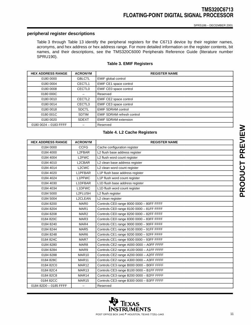
peripheral register descriptions
Table 3 through Table 13 identify the peripheral registers for the C6713 device by their register names,acronyms, and hex address or hex address range. For more detailed information on the register contents, bitnames, and their descriptions, see the TMS320C6000 Peripherals Reference Guide (literature numberSPRU190).
Table 3. EMIF Registers
HEX ADDRESS RANGE ACRONYM REGISTER NAME
0180 0000 GBLCTL EMIF global control
0180 0004 CECTL1 EMIF CE1 space control
0180 0008 CECTL0 EMIF CE0 space control
0180 000C – Reserved
0180 0010 CECTL2 EMIF CE2 space control
0180 0014 CECTL3 EMIF CE3 space control
0180 0018 SDCTL EMIF SDRAM control
0180 001C SDTIM EMIF SDRAM refresh control
0180 0020 SDEXT EMIF SDRAM extension
0180 0024 – 0183 FFFF – Reserved
Table 4. L2 Cache Registers
HEX ADDRESS RANGE ACRONYM REGISTER NAME
0184 0000 CCFG Cache configuration register
0184 4000 L2FBAR L2 flush base address register
0184 4004 L2FWC L2 flush word count register
0184 4010 L2CBAR L2 clean base address register
0184 4014 L2CWC L2 clean word count register
0184 4020 L1PFBAR L1P flush base address register
0184 4024 L1PFWC L1P flush word count register
0184 4030 L1DFBAR L1D flush base address register
0184 4034 L1DFWC L1D flush word count register
0184 5000 L2FLUSH L2 flush register
0184 5004 L2CLEAN L2 clean register
0184 8200 MAR0 Controls CE0 range 8000 0000 – 80FF FFFF
0184 8204 MAR1 Controls CE0 range 8100 0000 – 81FF FFFF
0184 8208 MAR2 Controls CE0 range 8200 0000 – 82FF FFFF
0184 820C MAR3 Controls CE0 range 8300 0000 – 83FF FFFF
0184 8240 MAR4 Controls CE1 range 9000 0000 – 90FF FFFF
0184 8244 MAR5 Controls CE1 range 9100 0000 – 91FF FFFF
0184 8248 MAR6 Controls CE1 range 9200 0000 – 92FF FFFF
0184 824C MAR7 Controls CE1 range 9300 0000 – 93FF FFFF
0184 8280 MAR8 Controls CE2 range A000 0000 – A0FF FFFF
0184 8284 MAR9 Controls CE2 range A100 0000 – A1FF FFFF
0184 8288 MAR10 Controls CE2 range A200 0000 – A2FF FFFF
0184 828C MAR11 Controls CE2 range A300 0000 – A3FF FFFF
0184 82C0 MAR12 Controls CE3 range B000 0000 – B0FF FFFF
0184 82C4 MAR13 Controls CE3 range B100 0000 – B1FF FFFF
0184 82C8 MAR14 Controls CE3 range B200 0000 – B2FF FFFF
0184 82CC MAR15 Controls CE3 range B300 0000 – B3FF FFFF
0184 82D0 – 0185 FFFF – Reserved
PR
OD
UC
T P
RE
VIE
W

TMS320C6713FLOATING-POINT DIGITAL SIGNAL PROCESSOR
SPRS186 – DECEMBER 2001
12 POST OFFICE BOX 1443 • HOUSTON, TEXAS 77251–1443
peripheral register descriptions (continued)
Table 5. Interrupt Selector Registers
HEX ADDRESS RANGE ACRONYM REGISTER NAME COMMENTS
019C 0000 MUXH Interrupt multiplexer high Selects which interrupts drive CPU interrupts10–15 (INT10–INT15)
019C 0004 MUXL Interrupt multiplexer low Selects which interrupts drive CPU interrupts 4–9(INT04–INT09)
019C 0008 EXTPOL External interrupt polarity Sets the polarity of the external interrupts(EXT_INT4–EXT_INT7)
019C 000C – 019F FFFF – Reserved
Table 6. EDMA Parameter RAM†
HEX ADDRESS RANGE ACRONYM REGISTER NAME
01A0 0000 – 01A0 0017 – Parameters for Event 0 (6 words)
01A0 0018 – 01A0 002F – Parameters for Event 1 (6 words)
01A0 0030 – 01A0 0047 – Parameters for Event 2 (6 words)
01A0 0048 – 01A0 005F – Parameters for Event 3 (6 words)
01A0 0060 – 01A0 0077 – Parameters for Event 4 (6 words)
01A0 0078 – 01A0 008F – Parameters for Event 5 (6 words)
01A0 0090 – 01A0 00A7 – Parameters for Event 6 (6 words)
01A0 00A8 – 01A0 00BF – Parameters for Event 7 (6 words)
01A0 00C0 – 01A0 00D7 – Parameters for Event 8 (6 words)
01A0 00D8 – 01A0 00EF – Parameters for Event 9 (6 words)
01A0 00F0 – 01A0 00107 – Parameters for Event 10 (6 words)
01A0 0108 – 01A0 011F – Parameters for Event 11 (6 words)
01A0 0120 – 01A0 0137 – Parameters for Event 12 (6 words)
01A0 0138 – 01A0 014F – Parameters for Event 13 (6 words)
01A0 0150 – 01A0 0167 – Parameters for Event 14 (6 words)
01A0 0168 – 01A0 017F – Parameters for Event 15 (6 words)
01A0 0180 – 01A0 0197 – Reload/link parameters for Event M (6 words)
01A0 0198 – 01A0 01AF – Reload/link parameters for Event N (6 words)
... ...
01A0 07E0 – 01A0 07F7 – Reload/link parameters for Event Z (6 words)
01A0 07F8 – 01A0 07FF – Scratch pad area (2 words)† The C6211/C6211B device has sixty-nine parameter sets [six (6) words each] that can be used to reload/link EDMA transfers.
PR
OD
UC
T P
RE
VIE
W

TMS320C6713FLOATING-POINT DIGITAL SIGNAL PROCESSOR
SPRS186 – DECEMBER 2001
13POST OFFICE BOX 1443 • HOUSTON, TEXAS 77251–1443
peripheral register descriptions (continued)
Table 7. EDMA Registers
HEX ADDRESS RANGE ACRONYM REGISTER NAME
01A0 0800 – 01A0 FEFC – Reserved
01A0 FF00 ESEL0 EDMA event selector 0
01A0 FF04 ESEL1 EDMA event selector 1
01A0 FF08 – Reserved
01A0 FF0C ESEL3 EDMA event selector 3
01A0 FF1F – 01A0 FFDC – Reserved
01A0 FFE0 PQSR Priority queue status register
01A0 FFE4 CIPR Channel interrupt pending register
01A0 FFE8 CIER Channel interrupt enable register
01A0 FFEC CCER Channel chain enable register
01A0 FFF0 ER Event register
01A0 FFF4 EER Event enable register
01A0 FFF8 ECR Event clear register
01A0 FFFC ESR Event set register
01A1 0000 – 01A3 FFFF – Reserved
Table 8. Quick DMA (QDMA) and Pseudo Registers†
HEX ADDRESS RANGE ACRONYM REGISTER NAME
0200 0000 QOPT QDMA options parameter register
0200 0004 QSRC QDMA source address register
0200 0008 QCNT QDMA frame count register
0200 000C QDST QDMA destination address register
0200 0010 QIDX QDMA index register
0200 0014 – 0200 001C – Reserved
0200 0020 QSOPT QDMA pseudo options register
0200 0024 QSSRC QDMA pseudo source address register
0200 0028 QSCNT QDMA pseudo frame count register
0200 002C QSDST QDMA pseudo destination address register
0200 0030 QSIDX QDMA pseudo index register† All the QDMA and Pseudo registers are write-accessible only
Table 9. PLL Wrapper Registers
HEX ADDRESS RANGE ACRONYM REGISTER NAME
01B7 C000 – 01B7 C0FF – Reserved
01B7 C100 PLLCSR PLL control/status register
01B7 C104 – 01B7 C10F – Reserved
01B7 C110 PLLM PLL multiplier control register
01B7 C114 PLLDIV0 PLL wrapper divider 0 register
01B7 C118 PLLDIV1 PLL wrapper divider 1 register
01B7 C11C PLLDIV2 PLL wrapper divider 2 register
01B7 C120 PLLDIV3 PLL wrapper divider 3 register
01B7 C124 OSCDIV1 Oscillator divider 1 register
01B7 C128 – 01B7 DFFF – Reserved
PR
OD
UC
T P
RE
VIE
W
TMS320C6713FLOATING-POINT DIGITAL SIGNAL PROCESSOR
SPRS186 – DECEMBER 2001
14 POST OFFICE BOX 1443 • HOUSTON, TEXAS 77251–1443
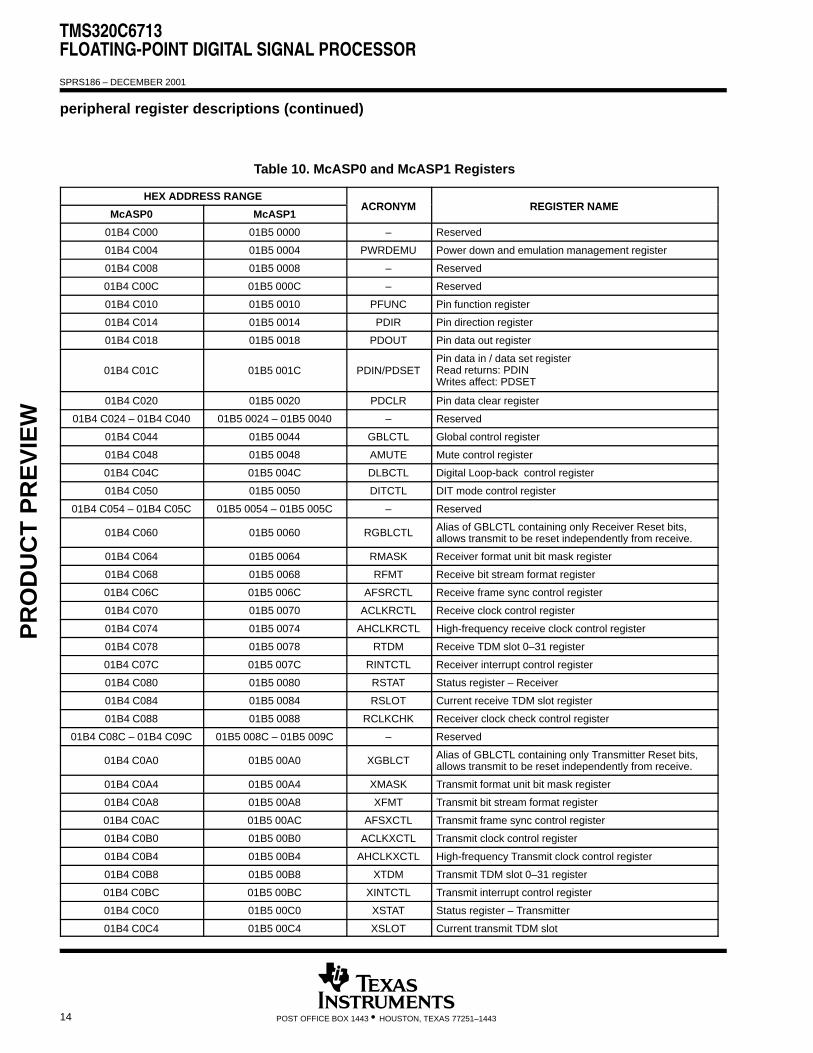
peripheral register descriptions (continued)
Table 10. McASP0 and McASP1 Registers
HEX ADDRESS RANGEACRONYM REGISTER NAME
McASP0 McASP1ACRONYM REGISTER NAME
01B4 C000 01B5 0000 – Reserved
01B4 C004 01B5 0004 PWRDEMU Power down and emulation management register
01B4 C008 01B5 0008 – Reserved
01B4 C00C 01B5 000C – Reserved
01B4 C010 01B5 0010 PFUNC Pin function register
01B4 C014 01B5 0014 PDIR Pin direction register
01B4 C018 01B5 0018 PDOUT Pin data out register
01B4 C01C 01B5 001C PDIN/PDSETPin data in / data set registerRead returns: PDINWrites affect: PDSET
01B4 C020 01B5 0020 PDCLR Pin data clear register
01B4 C024 – 01B4 C040 01B5 0024 – 01B5 0040 – Reserved
01B4 C044 01B5 0044 GBLCTL Global control register
01B4 C048 01B5 0048 AMUTE Mute control register
01B4 C04C 01B5 004C DLBCTL Digital Loop-back control register
01B4 C050 01B5 0050 DITCTL DIT mode control register
01B4 C054 – 01B4 C05C 01B5 0054 – 01B5 005C – Reserved
01B4 C060 01B5 0060 RGBLCTL Alias of GBLCTL containing only Receiver Reset bits,allows transmit to be reset independently from receive.
01B4 C064 01B5 0064 RMASK Receiver format unit bit mask register
01B4 C068 01B5 0068 RFMT Receive bit stream format register
01B4 C06C 01B5 006C AFSRCTL Receive frame sync control register
01B4 C070 01B5 0070 ACLKRCTL Receive clock control register
01B4 C074 01B5 0074 AHCLKRCTL High-frequency receive clock control register
01B4 C078 01B5 0078 RTDM Receive TDM slot 0–31 register
01B4 C07C 01B5 007C RINTCTL Receiver interrupt control register
01B4 C080 01B5 0080 RSTAT Status register – Receiver
01B4 C084 01B5 0084 RSLOT Current receive TDM slot register
01B4 C088 01B5 0088 RCLKCHK Receiver clock check control register
01B4 C08C – 01B4 C09C 01B5 008C – 01B5 009C – Reserved
01B4 C0A0 01B5 00A0 XGBLCT Alias of GBLCTL containing only Transmitter Reset bits,allows transmit to be reset independently from receive.
01B4 C0A4 01B5 00A4 XMASK Transmit format unit bit mask register
01B4 C0A8 01B5 00A8 XFMT Transmit bit stream format register
01B4 C0AC 01B5 00AC AFSXCTL Transmit frame sync control register
01B4 C0B0 01B5 00B0 ACLKXCTL Transmit clock control register
01B4 C0B4 01B5 00B4 AHCLKXCTL High-frequency Transmit clock control register
01B4 C0B8 01B5 00B8 XTDM Transmit TDM slot 0–31 register
01B4 C0BC 01B5 00BC XINTCTL Transmit interrupt control register
01B4 C0C0 01B5 00C0 XSTAT Status register – Transmitter
01B4 C0C4 01B5 00C4 XSLOT Current transmit TDM slot
PR
OD
UC
T P
RE
VIE
W

TMS320C6713FLOATING-POINT DIGITAL SIGNAL PROCESSOR
SPRS186 – DECEMBER 2001
15POST OFFICE BOX 1443 • HOUSTON, TEXAS 77251–1443
Table 10. McASP0 and McASP1 Registers (Continued)
HEX ADDRESS RANGEREGISTER NAMEACRONYM
McASP0REGISTER NAMEACRONYM
McASP1
01B4 C0C8 01B5 00C8 XCLKCHK Transmit clock check control register
01B4 C0CC – 01B4 C0FC 01B5 00CC – 01B5 00FC – Reserved
01B4 C100 01B5 0100 DITCSRA0 Left (even TDM slot) channel status register file
01B4 C104 01B5 0104 DITCSRA1 Left (even TDM slot) channel status register file
01B4 C108 01B5 0108 DITCSRA2 Left (even TDM slot) channel status register file
01B4 C10C 01B5 010C DITCSRA3 Left (even TDM slot) channel status register file
01B4 C110 01B5 0110 DITCSRA4 Left (even TDM slot) channel status register file
01B4 C114 01B5 0114 DITCSRA5 Left (even TDM slot) channel status register file
01B4 C118 01B5 0118 DITCSRB0 Right (odd TDM slot) channel status register file
01B4 C11C 01B5 011C DITCSRB1 Right (odd TDM slot) channel status register file
01B4 C120 01B5 0120 DITCSRB2 Right (odd TDM slot) channel status register file
01B4 C124 01B5 0124 DITCSRB3 Right (odd TDM slot) channel status register file
01B4 C128 01B5 0128 DITCSRB4 Right (odd TDM slot) channel status register file
01B4 C12C 01B5 012C DITCSRB5 Right (odd TDM slot) channel status register file
01B4 C130 01B5 0130 DITUDRA0 Left (even TDM slot) user data register file
01B4 C134 01B5 0134 DITUDRA1 Left (even TDM slot) user data register file
01B4 C138 01B5 0138 DITUDRA2 Left (even TDM slot) user data register file
01B4 C13C 01B5 013C DITUDRA3 Left (even TDM slot) user data register file
01B4 C140 01B5 0140 DITUDRA4 Left (even TDM slot) user data register file
01B4 C144 01B5 0144 DITUDRA5 Left (even TDM slot) user data register file
01B4 C148 01B5 0148 DITUDRB0 Right (odd TDM slot) user data register file
01B4 C14C 01B5 014C DITUDRB1 Right (odd TDM slot) user data register file
01B4 C150 01B5 0150 DITUDRB2 Right (odd TDM slot) user data register file
01B4 C154 01B5 0154 DITUDRB3 Right (odd TDM slot) user data register file
01B4 C158 01B5 0158 DITUDRB4 Right (odd TDM slot) user data register file
01B4 C15C 01B5 015C DITUDRB5 Right (odd TDM slot) user data register file
01B4 C160 – 01B4 C17C 01B5 0160 – 01B5 017C – Reserved
01B4 C180 01B5 0180 SRCTL0 Serializer 0 control register
01B4 C184 01B5 0184 SRCTL1 Serializer 1 control register
01B4 C188 01B5 0188 SRCTL2 Serializer 2 control register
01B4 C18C 01B5 018C SRCTL3 Serializer 3 control register
01B4 C190 01B5 0190 SRCTL4 Serializer 4 control register
01B4 C194 01B5 0194 SRCTL5 Serializer 5 control register
01B4 C198 01B5 0198 SRCTL6 Serializer 6 control register
01B4 C19C 01B5 019C SRCTL7 Serializer 7 control register
01B4 C1A0 – 01B4 C1FC 01B5 C1A0 – 01B5 01FC – Reserved
01B4 C200 01B5 0200 XBUF0 Transmit Buffer for Serializer 0
01B4 C204 01B5 0204 XBUF1 Transmit Buffer for Serializer 1
01B4 C208 01B5 0208 XBUF2 Transmit Buffer for Serializer 2
01B4 C20C 01B5 020C XBUF3 Transmit Buffer for Serializer 3
01B4 C210 01B50C210 XBUF4 Transmit Buffer for Serializer 4
PR
OD
UC
T P
RE
VIE
W
peripheral register descriptions (continued)

TMS320C6713FLOATING-POINT DIGITAL SIGNAL PROCESSOR
SPRS186 – DECEMBER 2001
16 POST OFFICE BOX 1443 • HOUSTON, TEXAS 77251–1443
Table 10. McASP0 and McASP1 Registers (Continued)
HEX ADDRESS RANGEREGISTER NAMEACRONYM
McASP0REGISTER NAMEACRONYM
McASP1
01B4 C214 01B5 0214 XBUF5 Transmit Buffer for Serializer 5
01B4 C218 01B5 0218 XBUF6 Transmit Buffer for Serializer 6
01B4 C21C 01B5 021C XBUF7 Transmit Buffer for Serializer 7
01B4 C220 – 01B4 C27C 01B5 C220 – 01B5 027C – Reserved
01B4 C280 01B5 0280 RBUF0 Receive Buffer for Serializer 0
01B4 C284 01B5 0284 RBUF1 Receive Buffer for Serializer 1
01B4 C288 01B5 0288 RBUF2 Receive Buffer for Serializer 2
01B4 C28C 01B5 028C RBUF3 Receive Buffer for Serializer 3
01B4 C290 01B5 0290 RBUF4 Receive Buffer for Serializer 4
01B4 C294 01B5 0294 RBUF5 Receive Buffer for Serializer 5
01B4 C298 01B5 0298 RBUF6 Receive Buffer for Serializer 6
01B4 C29C 01B5 029C RBUF7 Receive Buffer for Serializer 7
01B4 C2A0 – 01B4 FFFF 01B5 02A0 – 01B5 3FFF – Reserved
Table 11. I2C0 Registers
HEX ADDRESS RANGE ACRONYM REGISTER NAME
01B4 0000 I2COAR0 I2C0 own address register
01B4 0004 I2CIER0 I2C0 interrupt enable register
01B4 0008 I2CSTR0 I2C0 interrupt status register
01B4 000C I2CCLKL0 I2C0 clock low-time divider register
01B4 0010 I2CCLKH0 I2C0 clock high-time divider register
01B4 0014 I2CCNT0 I2C0 data count register
01B4 0018 I2CDRR0 I2C0 data receive register
01B4 001C I2CSAR0 I2C0 slave address register
01B4 0020 I2CDXR0 I2C0 data transmit register
01B4 0024 I2CMDR0 I2C0 mode register
01B4 0028 I2CISRC0 I2C0 interrupt source register
01B4 002C – Reserved
01B4 0030 I2CPSC0 I2C0 prescaler register
01B4 0034 – 01B4 3FFF – Reserved
PR
OD
UC
T P
RE
VIE
W
peripheral register descriptions (continued)

TMS320C6713FLOATING-POINT DIGITAL SIGNAL PROCESSOR
SPRS186 – DECEMBER 2001
17POST OFFICE BOX 1443 • HOUSTON, TEXAS 77251–1443
peripheral register descriptions (continued)
Table 12. I2C1 Registers
HEX ADDRESS RANGE ACRONYM REGISTER NAME
01B4 4000 I2COAR1 I2C1 own address register
01B4 4004 I2CIER1 I2C1 interrupt enable register
01B4 4008 I2CSTR1 I2C1 interrupt status register
01B4 400C I2CCLKL1 I2C1 clock low-time divider register
01B4 4010 I2CCLKH1 I2C1 clock high-time divider register
01B4 4014 I2CCNT1 I2C1 data count register
01B4 4018 I2CDRR1 I2C1 data receive register
01B4 401C I2CSAR1 I2C1 slave address register
01B4 4020 I2CDXR1 I2C1 data transmit register
01B4 4024 I2CMDR1 I2C1 mode register
01B4 4028 I2CISRC1 I2C1 interrupt source register
01B4 402C – Reserved
01B4 4030 I2CPSC1 I2C1 prescaler register
01B4 4034 – 01B4 7FFF – Reserved
Table 13. HPI Registers
HEX ADDRESS RANGE ACRONYM REGISTER NAME COMMENTS
– HPID HPI data register Host read/write access only
– HPIA HPI address register Host read/write access only
0188 0000 HPIC HPI control register Both Host/CPU read/write access
0188 0001 – 018B FFFF – Reserved
Table 14. McBSP 0 Registers
HEX ADDRESS RANGE ACRONYM REGISTER NAME COMMENTS
018C 0000 DRR0 McBSP0 data receive register via Peripheral Bus
The CPU and DMA/EDMAcontroller can only read thisregister; they cannot write toit.
0x3000 0000 – 0x33FF FFFF DRR0 McBSP0 data receive register via EDMA Bus
018C 0004 DXR0 McBSP0 data transmit register via Peripheral Bus
0x3000 0000 – 0x33FF FFFF DXR0 McBSP0 data transmit register via EDMA Bus
018C 0008 SPCR0 McBSP0 serial port control register
018C 000C RCR0 McBSP0 receive control register
018C 0010 XCR0 McBSP0 transmit control register
018C 0014 SRGR0 McBSP0 sample rate generator register
018C 0018 MCR0 McBSP0 multichannel control register
018C 001C RCER0 McBSP0 receive channel enable register
018C 0020 XCER0 McBSP0 transmit channel enable register
018C 0024 PCR0 McBSP0 pin control register
018C 0028 – 018F FFFF – Reserved
PR
OD
UC
T P
RE
VIE
W

TMS320C6713FLOATING-POINT DIGITAL SIGNAL PROCESSOR
SPRS186 – DECEMBER 2001
18 POST OFFICE BOX 1443 • HOUSTON, TEXAS 77251–1443
peripheral register descriptions (continued)
Table 15. McBSP 1 Registers
HEX ADDRESS RANGE ACRONYM REGISTER NAME COMMENTS
0190 0000 DRR1 Data receive register via Peripheral Bus
The CPU and DMA/EDMAcontroller can only read thisregister; they cannot write toit.
0x3400 0000 – 0x37FF FFFF DRR1 McBSP1 data receive register via EDMA Bus
0190 0004 DXR1 McBSP1 data transmit register via Peripheral Bus
0x3400 0000 – 0x37FF FFFF DXR1 McBSP1 data transmit register via EDMA Bus
0190 0008 SPCR1 McBSP1 serial port control register
0190 000C RCR1 McBSP1 receive control register
0190 0010 XCR1 McBSP1 transmit control register
0190 0014 SRGR1 McBSP1 sample rate generator register
0190 0018 MCR1 McBSP1 multichannel control register
0190 001C RCER1 McBSP1 receive channel enable register
0190 0020 XCER1 McBSP1 transmit channel enable register
0190 0024 PCR1 McBSP1 pin control register
0190 0028 – 0193 FFFF – Reserved
Table 16. Timer 0 Registers
HEX ADDRESS RANGE ACRONYM REGISTER NAME COMMENTS
0194 0000 CTL0 Timer 0 control registerDetermines the operating mode of the timer,monitors the timer status, and controls the functionof the TOUT pin.
0194 0004 PRD0 Timer 0 period registerContains the number of timer input clock cycles tocount. This number controls the TSTAT signalfrequency.
0194 0008 CNT0 Timer 0 counter register Contains the current value of the incrementingcounter.
0194 000C – 0197 FFFF – Reserved
Table 17. Timer 1 Registers
HEX ADDRESS RANGE ACRONYM REGISTER NAME COMMENTS
0198 0000 CTL1 Timer 1 control registerDetermines the operating mode of the timer,monitors the timer status, and controls the functionof the TOUT pin.
0198 0004 PRD1 Timer 1 period registerContains the number of timer input clock cycles tocount. This number controls the TSTAT signalfrequency.
0198 0008 CNT1 Timer 1 counter register Contains the current value of the incrementingcounter.
0198 000C – 019B FFFF – Reserved
PR
OD
UC
T P
RE
VIE
W
TMS320C6713FLOATING-POINT DIGITAL SIGNAL PROCESSOR
SPRS186 – DECEMBER 2001
19POST OFFICE BOX 1443 • HOUSTON, TEXAS 77251–1443
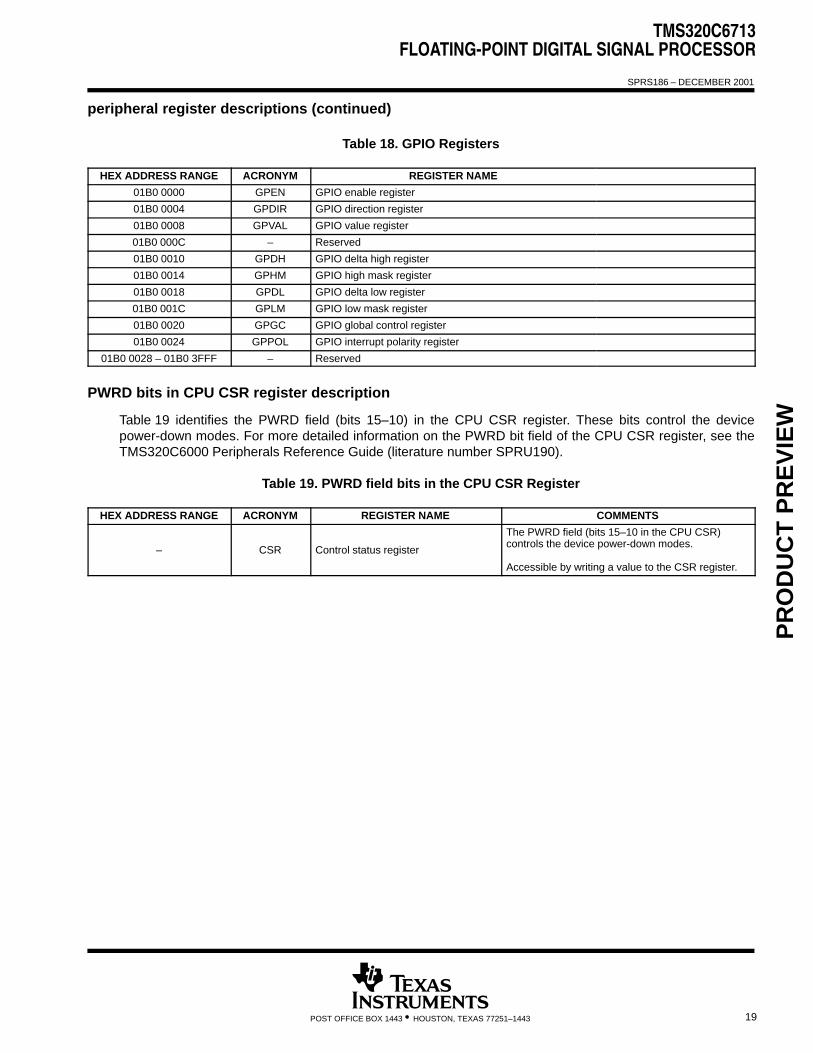
peripheral register descriptions (continued)
Table 18. GPIO Registers
HEX ADDRESS RANGE ACRONYM REGISTER NAME
01B0 0000 GPEN GPIO enable register
01B0 0004 GPDIR GPIO direction register
01B0 0008 GPVAL GPIO value register
01B0 000C – Reserved
01B0 0010 GPDH GPIO delta high register
01B0 0014 GPHM GPIO high mask register
01B0 0018 GPDL GPIO delta low register
01B0 001C GPLM GPIO low mask register
01B0 0020 GPGC GPIO global control register
01B0 0024 GPPOL GPIO interrupt polarity register
01B0 0028 – 01B0 3FFF – Reserved
PWRD bits in CPU CSR register description
Table 19 identifies the PWRD field (bits 15–10) in the CPU CSR register. These bits control the devicepower-down modes. For more detailed information on the PWRD bit field of the CPU CSR register, see theTMS320C6000 Peripherals Reference Guide (literature number SPRU190).
Table 19. PWRD field bits in the CPU CSR Register
HEX ADDRESS RANGE ACRONYM REGISTER NAME COMMENTS
– CSR Control status register
The PWRD field (bits 15–10 in the CPU CSR)controls the device power-down modes.
Accessible by writing a value to the CSR register.
PR
OD
UC
T P
RE
VIE
W

TMS320C6713FLOATING-POINT DIGITAL SIGNAL PROCESSOR
SPRS186 – DECEMBER 2001
20 POST OFFICE BOX 1443 • HOUSTON, TEXAS 77251–1443
interrupts and interrupt selector
The C67x DSP core supports 16 prioritized interrupts, which are listed in Table 20. The highest priority interruptis INT_00 (dedicated to RESET) while the lowest priority is INT_15. The first four interrupts are non-maskableand fixed. The remaining interrupts (4–15) are maskable and default to the interrupt source listed in Table 20.However, their interrupt source may be reprogrammed to any one of the sources listed in Table 21 (InterruptSelector). Table 21 lists the selector value corresponding to each of the alternate interrupt sources. The selectorchoice for interrupts 4–15 is made by programming the corresponding fields (listed in Table 20) in the MUXH(address 0x019C0000) and MUXL (address 0x019C0004) registers.
Table 20. DSP Interrupts Table 21. Interrupt Selector
DSPINTERRUPT
NUMBER
INTERRUPTSELECTORCONTROLREGISTER
DEFAULTSELECTOR
VALUE(BINARY)
DEFAULTINTERRUPT
EVENT
INTERRUPTSELECTOR
VALUE(BINARY)
INTERRUPTEVENT MODULE
INT_00 – – RESET 00000 DSPINT HPI
INT_01 – – NMI 00001 TINT0 Timer 0
INT_02 – – Reserved 00010 TINT1 Timer 1
INT_03 – – Reserved 00011 SDINT EMIF
INT_04 MUXL[4:0] 00100 EXTINT4 00100 EXTINT4 GPIO
INT_05 MUXL[9:5] 00101 EXTINT5 00101 EXTINT5 GPIO
INT_06 MUXL[14:10] 00110 EXTINT6 00110 EXTINT6 GPIO
INT_07 MUXL[20:16] 00111 EXTINT7 00111 EXTINT7 GPIO
INT_08 MUXL[25:21] 01000 EDMAINT 01000 EDMAINT EDMA
INT_09 MUXL[30:26] 01001 EMUDTDMA 01001 EMUDTDMA Emulation
INT_10 MUXH[4:0] 00011 SDINT 01010 EMURTDXRX Emulation
INT_11 MUXH[9:5] 01010 EMURTDXRX 01011 EMURTDXTX Emulation
INT_12 MUXH[14:10] 01011 EMURTDXTX 01100 XINT0 McBSP0
INT_13 MUXH[20:16] 00000 DSPINT 01101 RINT0 McBSP0
INT_14 MUXH[25:21] 00001 TINT0 01110 XINT1 McBSP1
INT_15 MUXH[30:26] 00010 TINT1 01111 RINT1 McBSP1
10000 GPINT0 GPIO
10001 Reserved –
10010 Reserved –
10011 Reserved –
10100 Reserved –
10101 Reserved –
10110 I2CINT0 I2C0
10111 I2CINT1 I2C1
11000 Reserved –
11001 Reserved –
11010 Reserved –
11011 Reserved –
11100 AXINT0 McASP0
11101 ARINT0 McASP0
11110 AXINT1 McASP1
11111 ARINT1 McASP1
PR
OD
UC
T P
RE
VIE
W

TMS320C6713FLOATING-POINT DIGITAL SIGNAL PROCESSOR
SPRS186 – DECEMBER 2001
21POST OFFICE BOX 1443 • HOUSTON, TEXAS 77251–1443
EDMA module and EDMA selector
The C67x EDMA supports up to 16 EDMA channels. Four of the sixteen channels (channels 8–11) are reservedfor EDMA chaining, leaving 12 EDMA channels available to service peripheral devices.
The EDMA selector registers that control the EDMA channels servicing peripheral devices are located ataddresses 0x01A0FF00 (ESEL0), 0x01A0FF04 (ESEL1), and 0x01A0FF0C (ESEL3). These EDMA selectorregisters control the mapping of the EDMA events to the EDMA channels. Each EDMA event has an assignedEDMA selector code (see Table 23). By loading each EVTSELx register field with an EDMA selector code, userscan map any desired EDMA event to any specified EDMA channel. Table 22 lists the default EDMA selectorvalue for each EDMA channel.
See Table 24 and Table 25 for the EDMA Event Selector registers and their assoicated bit descriptions.
PR
OD
UC
T P
RE
VIE
W

TMS320C6713FLOATING-POINT DIGITAL SIGNAL PROCESSOR
SPRS186 – DECEMBER 2001
22 POST OFFICE BOX 1443 • HOUSTON, TEXAS 77251–1443
EDMA module and EDMA selector (continued)
Table 22. EDMA Channels Table 23. EDMA Selector
EDMACHANNEL
EDMASELECTORCONTROLREGISTER
DEFAULTSELECTOR
VALUE(BINARY)
DEFAULTEDMAEVENT
EDMASELECTOR
CODE (BINARY)
EDMAEVENT MODULE
0 ESEL0[5:0] 000000 DSPINT 000000 DSPINT HPI
1 ESEL0[13:8] 000001 TINT0 000001 TINT0 TIMER0
2 ESEL0[21:16] 000010 TINT1 000010 TINT1 TIMER1
3 ESEL0[29:24] 000011 SDINT 000011 SDINT EMIF
4 ESEL1[5:0] 000100 EXTINT4 000100 EXTINT4 GPIO
5 ESEL1[13:8] 000101 EXTINT5 000101 EXTINT5 GPIO
6 ESEL1[21:16] 000110 EXTINT6 000110 EXTINT6 GPIO
7 ESEL1[29:24] 000111 EXTINT7 000111 EXTINT7 GPIO
8 n/a n/a TCC8 (Chaining) 001000 GPINT0 GPIO
9 n/a n/a TCC9 (Chaining) 001001 GPINT1 GPIO
10 n/a n/a TCC10 (Chaining) 001010 GPINT2 GPIO
11 n/a n/a TCC11 (Chaining) 001011 GPINT3 GPIO
12 ESEL3[5:0] 001000 XEVT0 001100 XEVT0 McBSP0
13 ESEL3[13:8] 001001 REVT0 001101 REVT0 McBSP0
14 ESEL3[21:16] 001010 XEVT1 001110 XEVT1 McBSP1
15 ESEL3[29:24] 001011 REVT1 001111 REVT1 McBSP1
010000–011111 Reserved
100000 AXEVTE0 McASP0
100001 AXEVTO0 McASP0
100010 AXEVT0 McASP0
100011 AREVTE0 McASP0
100100 AREVTO0 McASP0
100101 AREVT0 McASP0
100110 AXEVTE1 McASP1
100111 AXEVTO1 McASP1
101000 AXEVT1 McASP1
101001 AREVTE1 McASP1
101010 AREVTO1 McASP1
101011 AREVT1 McASP1
101100 I2CREVT0 I2C0
101101 I2CXEVT0 I2C0
101110 I2CREVT1 I2C1
101111 I2CXEVT1 I2C1
110000 GPINT8 GPIO
110001 GPINT9 GPIO
110010 GPINT10 GPIO
110011 GPINT11 GPIO
110100 GPINT12 GPIO
110101 GPINT13 GPIO
110110 GPINT14 GPIO
110111 GPINT15 GPIO
111000–111111 Reserved
PR
OD
UC
T P
RE
VIE
W

TMS320C6713FLOATING-POINT DIGITAL SIGNAL PROCESSOR
SPRS186 – DECEMBER 2001
23POST OFFICE BOX 1443 • HOUSTON, TEXAS 77251–1443
EDMA module and EDMA selector (continued)
Table 24. EDMA Event Selector Registers (ESEL0, ESEL1, and ESEL3)
ESEL0 Register (0x01A0 FF00)
31 30 29 28 27 24 23 22 21 20 19 16
Reserved EVTSEL3 Reserved EVTSEL2
R–0 R/W–00 0011b R–0 R/W–00 0010b
15 14 13 12 11 8 7 6 5 4 3 0
Reserved EVTSEL1 Reserved EVTSEL0
R–0 R/W–00 0001b R–0 R/W–00 0000b
Legend: R = Read only, R/W = Read/Write; -n = value after reset
ESEL1 Register (0x01A0 FF04)
31 30 29 28 27 24 23 22 21 20 19 16
Reserved EVTSEL7 Reserved EVTSEL6
R–0 R/W–00 0111b R–0 R/W–00 0110b
15 14 13 12 11 8 7 6 5 4 3 0
Reserved EVTSEL5 Reserved EVTSEL4
R–0 R/W–00 0101b R–0 R/W–00 0100b
Legend: R = Read only, R/W = Read/Write; -n = value after reset
ESEL3 Register (0x01A0 FF0C)
31 30 29 28 27 24 23 22 21 20 19 16
Reserved EVTSEL15 Reserved EVTSEL14
R–0 R/W–00 1011b R–0 R/W–00 1010b
15 14 13 12 11 8 7 6 5 4 3 0
Reserved EVTSEL13 Reserved EVTSEL12
R–0 R/W–00 1001b R–0 R/W–00 1000b
Legend: R = Read only, R/W = Read/Write; -n = value after reset
Table 25. EDMA Event Selection Registers (ESEL0, ESEL1, and ESEL3) Description
BIT # NAME DESCRIPTION
31:3023:2215:147:6
Reserved Reserved. Read-only, writes have no effect.
29:2421:1613:85:0
EVTSELx
EDMA event selection bits for channel x. Allows mapping of the EDMA events to the EDMA channels.
The EVTSEL0 through EVTSEL15 bits correspond to the channels 0 to 15, respectively. TheseEVTSELx fileds are user–selectable. By configuring the EVTSELx fields to the EDMA selector valueof the desired EDMA sync event number (see Table 23), users can map any EDMA event to theEDMA channel.
For example, if EVTSEL15 is programmed to 00 0001b (the EDMA selector code for TINT0), thenchannel 15 is triggered by Timer0 TINT0 events.
PR
OD
UC
T P
RE
VIE
W

TMS320C6713FLOATING-POINT DIGITAL SIGNAL PROCESSOR
SPRS186 – DECEMBER 2001
24 POST OFFICE BOX 1443 • HOUSTON, TEXAS 77251–1443
signal groups description
TRST
GP[7](EXT_INT7)
IEEE Standard1149.1(JTAG)
Emulation
Reset andInterrupts
Control/Status
TDITDOTMS
TCK
EMU0EMU1
NMI
GP[6](EXT_INT6)GP[5](EXT_INT5)/AMUTEIN0GP[4](EXT_INT4)/AMUTEIN1
RESET
Clock/PLLOscillator
CLKIN
CLKMODE0
PLLVPLLG
CLKOUT2/GP[2]
EMU2†
EMU3†
EMU4†
EMU5†
OSCINOSCOUT
HHWIL/AFSR1
HCNTL0/AXR1[3]
HCNTL1/AXR1[1]
Data
Register Select
Half-WordSelect
Control
HPI(Host-Port Interface)
HAS/ACLKX1HR/W/AXR1[0]HCS/AXR1[2]HDS1/AXR1[6]HDS2/AXR1[5]HRDY/ACLKR1HINT/GP[1]
HD15/GP[15]HD14/GP[14]HD13/GP[13]HD12/GP[12]HD11/GP[11]HD10/GP[10]
HD9/GP[9]HD8/GP[8]HD7/GP[3]
HD6/AHCLKR1HD5/AHCLKX1
HD4/GP[0]HD3/AMUTE1
HD2/AFSX1HD1/AXR1[7]HD0/AXR1[4]
CLKOUT3
†These external pins are applicable to the GFN package only.
NOTE A: On multiplexed pins, bolded text denotes the active function of the pin for that particular peripheral module.
Figure 3. CPU (DSP Core) and Peripheral Signals
PR
OD
UC
T P
RE
VIE
W

TMS320C6713FLOATING-POINT DIGITAL SIGNAL PROCESSOR
SPRS186 – DECEMBER 2001
25POST OFFICE BOX 1443 • HOUSTON, TEXAS 77251–1443
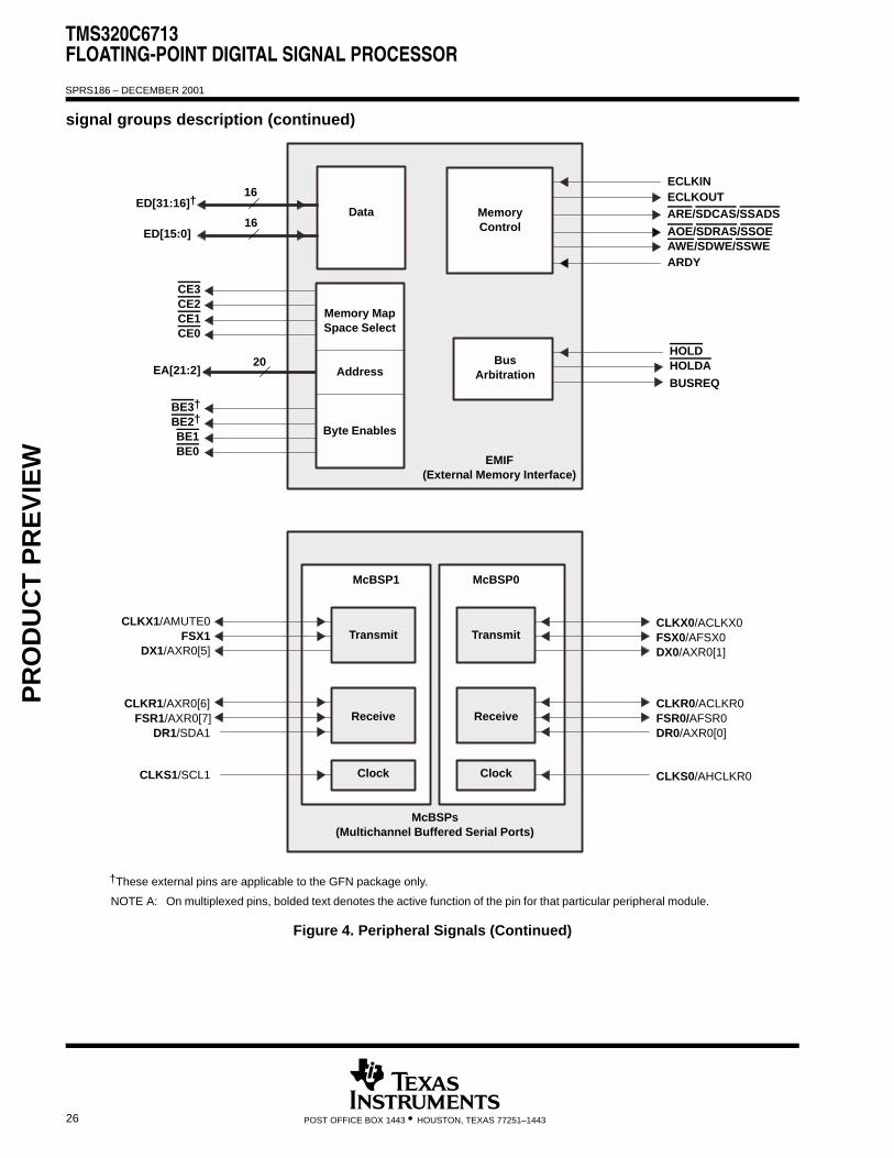
signal groups description (continued)
General-Purpose Input/Output (GPIO) Port
GP[7](EXT_INT7)GP[6](EXT_INT6)GP[5](EXT_INT5)/AMUTEIN0GP[4](EXT_INT4)/AMUTEIN1HD7/GP[3]CLKOUT2/GP[2]HINT/GP[1]HD4/GP[0]
GPIO
HD15/GP[15]HD14/GP[14]HD13/GP[13]HD12/GP[12]HD11/GP[11]HD10/GP[10]
HD9/GP[9]HD8/GP[8]
TOUT1/AXR0[4] TOUT0/AXR0[2]Timer 1 Timer 0
Timers
TINP1/AHCLKX0 TINP0/AXR0[3]
CLKS1/SCL1 SCL0I2C1 I2C0
I2Cs
DR1/SDA1 SDA0
NOTE A: On multiplexed pins, bolded text denotes the active function of the pin for that particular peripheral module.
Figure 4. Peripheral Signals PR
OD
UC
T P
RE
VIE
W
TMS320C6713FLOATING-POINT DIGITAL SIGNAL PROCESSOR
SPRS186 – DECEMBER 2001
26 POST OFFICE BOX 1443 • HOUSTON, TEXAS 77251–1443
signal groups description (continued)
CE3
ECLKOUTED[31:16]†
CE2CE1CE0
EA[21:2]
BE3†
BE2†
BE1BE0
CLKX1/AMUTE0FSX1
DX1/AXR0[5]
CLKR1/AXR0[6]FSR1/AXR0[7]
DR1/SDA1
CLKS1/SCL1
AOE/SDRAS/SSOEAWE/SDWE/SSWEARDY
CLKX0/ACLKX0FSX0/AFSX0DX0/AXR0[1]
CLKR0/ACLKR0FSR0/AFSR0DR0/AXR0[0]
CLKS0/AHCLKR0
Data
Memory MapSpace Select
Address
Byte Enables
16
20
MemoryControl
EMIF(External Memory Interface)
Receive Receive
McBSP1 McBSP0
Transmit Transmit
Clock Clock
McBSPs(Multichannel Buffered Serial Ports)
ECLKIN
HOLDHOLDA
BUSREQ
BusArbitration
ARE/SDCAS/SSADS
†These external pins are applicable to the GFN package only.
ED[15:0]16
NOTE A: On multiplexed pins, bolded text denotes the active function of the pin for that particular peripheral module.
Figure 4. Peripheral Signals (Continued)
PR
OD
UC
T P
RE
VIE
W

TMS320C6713FLOATING-POINT DIGITAL SIGNAL PROCESSOR
SPRS186 – DECEMBER 2001
27POST OFFICE BOX 1443 • HOUSTON, TEXAS 77251–1443
signal groups description (continued)
McASP0(Multichannel Audio Serial Port 0)
CLKX0/ACLKX0
CLKS0/AHCLKR0
TransmitClock
Generator
GP[5](EXT_INT5)/AMUTEIN0Auto Mute
Logic
CLKX1/AMUTE0
FSX0/AFSX0TransmitFrame Sync
FSR0/AFSR0 ReceiveFrame Sync
CLKR0/ACLKR0TINP1/AHCLKX0
Receive ClockGenerator
TOUT1/AXR0[4]
TOUT0/AXR0[2]DX0/AXR0[1]DR0/AXR0[0]
DX1/AXR0[5]
TINP0/AXR0[3]
CLKR1/AXR0[6]FSR1/AXR0[7]
8-Serial Ports Flexible
Partitioning Tx, Rx, OFF
TransmitClock Check
Circuit
Receive ClockCheck Circuit
Error Detect(see Note A)
(Transmit/Receive Data Pins)
(Receive Bit Clock) (Transmit Bit Clock)
(Receive Master Clock) (Transmit Master Clock)
(Receive Frame Sync orLeft/Right Clock)
(Transmit Frame Sync orLeft/Right Clock)
NOTES: A. The McASPs’ Error Detect function detects underruns, overruns, early/late frame syncs, DMA errors, and external mute input.B. On multiplexed pins, bolded text denotes the active function of the pin for that particular peripheral module.C. Bolded and italicized text within parentheses denotes the function of the pins in an audio system.
Figure 4. Peripheral Signals (Continued)
PR
OD
UC
T P
RE
VIE
W

TMS320C6713FLOATING-POINT DIGITAL SIGNAL PROCESSOR
SPRS186 – DECEMBER 2001
28 POST OFFICE BOX 1443 • HOUSTON, TEXAS 77251–1443
signal groups description (continued)
HD0/AXR1[4]
HCS/AXR1[2]HCNTL1/AXR1[1]
HR/W/AXR1[0]
McASP1(Multichannel Audio Serial Port 1)
HDS2/AXR1[5]
HAS/ACLKX1
HD5/AHCLKX1
TransmitClock
Generator
HCNTL0/AXR1[3]
GP[4](EXT_INT4)/AMUTEIN1Auto Mute
LogicHD3/AMUTE1
HD2/AFSX1TransmitFrame Sync
HHWIL/AFSR1 ReceiveFrame Sync
HDS1/AXR1[6]HD1/AXR1[7]
HRDY/ACLKR1HD6/AHCLKR1
Receive ClockGenerator
8-Serial Ports Flexible
Partitioning Tx, Rx, OFF
TransmitClock Check
Circuit
Receive ClockCheck Circuit
Error Detect(see Note A)
(Transmit/Receive Data Pins)
(Receive Bit Clock) (Transmit Bit Clock)
(Receive Master Clock) (Transmit Master Clock)
(Receive Frame Sync orLeft/Right Clock)
(Transmit Frame Sync orLeft/Right Clock)
NOTES: A. The McASPs’ Error Detect function detects underruns, overruns, early/late frame syncs, DMA errors, and external mute input.B. On multiplexed pins, bolded text denotes the active function of the pin for that particular peripheral module.C. Bolded and italicized text within parentheses denotes the function of the pins in an audio system.
Figure 4. Peripheral Signals (Continued)
PR
OD
UC
T P
RE
VIE
W

TMS320C6713FLOATING-POINT DIGITAL SIGNAL PROCESSOR
SPRS186 – DECEMBER 2001
29POST OFFICE BOX 1443 • HOUSTON, TEXAS 77251–1443
DEVICE CONFIGURATIONS
On the C6713 device, bootmode and certain device configurations/peripheral selections are determined atdevice reset, while other device configurations/peripheral selections are software-configurable via the deviceconfigurations register (DEVCFG) [address location 0x019C0200] after device reset.
device configurations at device reset
Table 26 describes the C6713 device configuration pins, which are set up via external pullup/pulldown resistorsthrough the HPI data pins (HD[4:3], HD8, and HD12) and CLKMODE0 pin. For more details on these deviceconfiguration pins, see the Terminal Functions table and the Debugging Considerations section.
Table 26. Device Configurations Pins at Device Reset (HD[4:3], HD8, HD12, and CLKMODE0)†
CONFIGURATIONPIN PYP GFN FUNCTIONAL DESCRIPTION
HD8 B17Device Endian mode (LEND)
0 – System operates in Big Endian mode1 – System operates in Little Endian mode (default)
HD[4:3](BOOTMODE)
A15, C19, C20
Bootmode Configuration Pins (BOOTMODE)00 – CE1 width 32-bit, HPI boot01 – CE1 width 8-bit, Asynchronous external ROM boot with default
timings (default mode)10 – CE1 width 16-bit, Asynchronous external ROM boot11 – CE1 width 32-bit, Asynchronous external ROM boot
HD12 C15Pulldown. For proper device operation, this pin must be externally pulled downwith a 1-kΩ resistor.
CLKMODE0 C4
Clock generator input clock source select 0 – Oscillator pads (OSCIN, OSCOUT directly from the crystal
oscillator) 1 – CLKIN square wave [default]
This pin must be pulled to the correct level even after reset.† Other HD pins (HD [15, 13, 11:9, 7:5, 2:0] have pullups/pulldowns (IPUs/IPDs). For proper device operation, do not oppose these pins with
external IPUs/IPDs at reset. PR
OD
UC
T P
RE
VIE
W

TMS320C6713FLOATING-POINT DIGITAL SIGNAL PROCESSOR
SPRS186 – DECEMBER 2001
30 POST OFFICE BOX 1443 • HOUSTON, TEXAS 77251–1443
DEVICE CONFIGURATIONS (CONTINUED)
peripheral selection at device reset
Some C6713 peripherals share the same pins but are mutually exclusive (i.e., HPI, general-purposeinput/output 0 pins GP[15:8, 3, 1, 0], McASP0, and I2C0).
HPI versus McASP1, I2C0, and GP peripherals
The HPI_EN (HD14 pin) is latched at reset. This pin selects whether the HPI peripheral or McASP1, I2C0peripherals, and GP[15:8, 3, 1, 0] pins are functionally enabled (see Table 27).
Table 27. HPI_EN (HD14 Pin) Peripheral Selection (HPI or McASP1, I2C0, and Select GP Pins)
PERIPHERAL SELECTION PERIPHERALS SELECTED
HPI_EN (HD14 Pin) HPI
McASP1, I2C0,and GP
[15:8,3,1,0]
DESCRIPTION
0 √
HPI_EN = 0HPI is disabled; McASP1 and I2C0 peripherals and GP [15:8, 3, 1,0] pinsare enabled. All multiplexed HPI/McASP1 and HPI/GP pins function asMcASP1 and GP pins, respectively. To use the GP pins, the appropriatebits in the GPEN and GPDIR registers need to be configured.
The IPUs on the I2C0 pins are disabled, allowing for I2C0 use. When the I2C0 peripheral is not used, to avoid floating inputs, these I2C0pins must be externally pulled up with 1-kΩ resistor.
1 √
HPI_EN = 1HPI is enabled; McASP1 and I2C0 peripherals and GP [15:8, 3, 1,0] pinsare disabled [default]. All multiplexed HPI/McASP1 and HPI/GP pinsfunction as HPI pins.
In addition, since the I2C0 peripheral is disabled, the IPUs on the I2C0pins are enabled to avoid floating inputs.
PR
OD
UC
T P
RE
VIE
W

TMS320C6713FLOATING-POINT DIGITAL SIGNAL PROCESSOR
SPRS186 – DECEMBER 2001
31POST OFFICE BOX 1443 • HOUSTON, TEXAS 77251–1443
DEVICE CONFIGURATIONS (CONTINUED)
peripheral selection/device configurations via the DEVCFG control register
The device configuration register (DEVCFG) allows the user to control the peripheral selection of the McBSP0,McBSP1, McASP0, and I2C1 peripherals. The DEVCFG register also offers the user control of the EMIF inputclock source and the timer output functions of the TOUT1/AXR0[4] and TOUT0/AXR0[2] multiplexed pins. Formore detailed information on the DEVCFG register control bits, see Table 28 and Table 29.
Table 28. Device Configuration Register (DEVCFG) [Address location: 0x019C0200]
31 16
Reserved†
RW-0
15 5 4 3 2 1 0
Reserved† EKSRC TOUT1SEL TOUT0SEL McASP0EN I2C1EN
RW-0 R/W-0 R/W-0 R/W-0 R/W-0 R/W-0
Legend: R/W = Read/Write; -n = value after reset† Do not write non-zero values to these bit locations.
Table 29. Device Configuration (DEVCFG) Register Selection Bit Descriptions
BIT # NAME DESCRIPTION
31:5 Reserved Reserved. Do not write non-zero values to these bit locations.
4 EKSRC
EMIF input clock source bit.Determines which clock signal is used as the EMIF input clock.
0 = SYSCLK3 (from the clock generator) is the EMIF input clock source (default) 1 = ECLKIN external pin is the EMIF input clock source
3 TOUT1SEL
Timer 1 output (TOUT1) pin function select bit.Selects the pin function of the TOUT1/AXR0[4] external pin independent of the rest of the peripheralselection bits in the DEVCFG register.
0 = The pin functions as a Timer 1 output (TOUT1) pin (default) 1 = The pin functions as the McASP0 AXR0[4] pin.
2 TOUT0SEL
Timer 0 output (TOUT0) pin function select bit.Selects the pin function of the TOUT0/AXR0[2] external pin independent of the rest of the peripheralselection bits in the DEVCFG register.
0 = The pin functions as a Timer 0 output (TOUT0) pin (default) 1 = The pin functions as the McASP0 AXR0[2] pin.
1 MCASP0EN
Multichannel Audio Serial Port 0 (McASP0) enable bit.Selects whether McASP0 or the McBSP0 peripheral is enabled.
0 = McASP0 is disabled (functional for DIT mode only), McBSP0 is enabled (default).1 = McASP0 is enabled, McBSP0 is disabled.
0 I2C1EN
Inter-integrated circuit 1 (I2C1) enable bit.Selects whether I2C1 or the McBSP1 peripheral is enabled.
0 = I2C1 is disabled, McBSP1 is enabled (default)The internal IPU/IPDs on the CLKS1/SCL1 and DR1/SDA1 pins are enabled for McBSP1’s use.
1 = I2C1 is enabled, McBSP1 is disabled The internal IPU/IPDs on the CLKS1/SCL1 and DR1/SDA1 pins are disabled for I2C1’s use
PR
OD
UC
T P
RE
VIE
W

TMS320C6713FLOATING-POINT DIGITAL SIGNAL PROCESSOR
SPRS186 – DECEMBER 2001
32 POST OFFICE BOX 1443 • HOUSTON, TEXAS 77251–1443
DEVICE CONFIGURATIONS (CONTINUED)
multiplexed pins
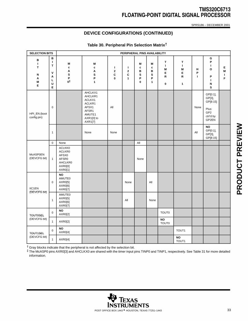
Multiplexed pins are pins that are shared by more than one peripheral and are internally multiplexed. Most ofthese pins are configured by software via the device configuration register (DEVCFG), and the others(specifically, the HPI pins) are configured by an external pullup/pulldown resistor on the HD14 pin (HPI_EN) atreset. The muxed pins that are configured by software are intended to be programmed once during softwareinitialization. The muxed pins that are configured by external pullup/pulldown resistors are mutually exclusive;only one peripheral has primary control of the function of these pins after reset. Table 30 summarizes theperipheral pins affected by the HPI_EN (HD14 pin) and DEVCFG register. Table 31 identifies the multiplexedpins on the C6713 device; shows the default (primary) function and the default settings after reset; anddescribes the pins, registers, etc. necessary to configure the specific multiplexed functions.
PR
OD
UC
T P
RE
VIE
W
TMS320C6713FLOATING-POINT DIGITAL SIGNAL PROCESSOR
SPRS186 – DECEMBER 2001
33POST OFFICE BOX 1443 • HOUSTON, TEXAS 77251–1443
DEVICE CONFIGURATIONS (CONTINUED)
Table 30. Peripheral Pin Selection Matrix†
SELECTION BITS PERIPHERAL PINS AVAILABILITY
BIT
NAME
BIT
VALUE
McASP0‡
McASP1
I2C0
I2C1
McBSP0
McBSP1
TIMER
0
TIMER
1
HPI
GPIO
PINS
EMIF
HPI_EN (bootconfig pin)
0
AHCLKX1AHCLKR1ACLKX1ACLKR1AFSX1AFSR1AMUTE1AXR1[0] toAXR1[7]
All None
GP[0:1],GP[3],GP[8:15]
Plus:GP2ctrl’d byGP2EN
1 None None All
NOGP[0:1],GP[3],GP[8:15]
0 None All
McASP0EN(DEVCFG bit) 1
ACLKK0ACLKR0AFSX0AFSR0AHCLKR0AXR0[0]AXR0[1]
None
IIC1EN(DEVCFG bit)
0
NOAMUTE0AXR0[5]AXR0[6]AXR0[7]
None All
(DEVCFG bit)
1
AMUTE0AXR0[5]AXR0[6]AXR0[7]
All None
TOUT0SEL0
NOAXR0[2]
TOUT0TOUT0SEL(DEVCFG bit)
1 AXR0[2]NOTOUT0
TOUT1SEL0
NOAXR0[4]
TOUT1TOUT1SEL(DEVCFG bit)
1 AXR0[4]NOTOUT1
† Gray blocks indicate that the peripheral is not affected by the selection bit.‡ The McASP0 pins AXR0[3] and AHCLKX0 are shared with the timer input pins TINP0 and TINP1, respectively. See Table 31 for more detailed
information.
PR
OD
UC
T P
RE
VIE
W

TMS320C6713FLOATING-POINT DIGITAL SIGNAL PROCESSOR
SPRS186 – DECEMBER 2001
34 POST OFFICE BOX 1443 • HOUSTON, TEXAS 77251–1443
DEVICE CONFIGURATIONS (CONTINUED)
Table 31. C6713 Device Multiplexed/Shared Pins
MULTIPLEXED PINSDEFAULT FUNCTION DEFAULT SETTING DESCRIPTION
NAME PYP GFNDEFAULT FUNCTION DEFAULT SETTING DESCRIPTION
CLKOUT2/GP[2] Y12 CLKOUT2
GP2EN = 0 (GPEN reigster bit)GP[2] function disabled,CLKOUT2 enabled
When the CLKOUT2 pin is enabled ,the CLK2EN bit in the EMIF globalcontrol register (GBLCTL) controlsthe CLKOUT2 pin.
CLK2EN = 0: CLKOUT2 heldhigh
CLK2EN = 1: CLKOUT2 enabled to clock
To use these as GPIO pins, theGPxEN bits in the GPIO EnableRegister and the GPxDIR bits in the
GP[5](EXT_INT5)/AMUTEIN0GP[4](EXT_INT4)/AMUTEIN1
C1C2
GP[5](EXT_INT5)GP[4](EXT_INT4)
No FunctionGP5EN = 0 (disabled)GP4EN = 0 (disabled)GPxDIR = 0 (input)
Register and the GPxDIR bits in theGPIO Direction Register must beproperly configured.
GPxEN = 1: GPx pin enabledGPxDIR = 0: GPx pin is an inputGPxDIR = 1: GPx pin is an
output
To use AMUTEIN0/1 pin function,the GP[5]/GP[4] pins must beconfigured as an input, and set to 1the INSTAT bit in the associatedMcASP AMUTE register.
CLKS0/AHCLKR0 K3
DR0/AXR0[0] J1
DX0/AXR0[1] H2 MCASP0EN = 0(DEVCFG i bi )
To enable the McASP0 peripheral, theM ASP0EN bi i h DEVCFGFSR0/AFSR0 J3 McBSP0 pin function
(DEVCFG register bit)McASP0 pins disabled
McASP0EN bit in the DEVCFGregister must be set to 1 (disabling the
FSX0/AFSX0 H1
McBSP0 in function McASP0 pins disabled, McBSP0 pins enabled
register must be set to 1 (disabling theMcBSP0 peripheral pins).
CLKR0/ACLKR0 H3McBSP0 ins enabled McBSP0 eri heral ins).
CLKX0/ACLKX0 G3
CLKS1/SCL1 E1
McBSP1 pin function
I2C1EN = 0(DEVCFG register bit)
To enable the I2C1 peripheral, theI2C1EN bit in the DEVCFG register
DR1/SDA1 M2McBSP1 pin function
(DEVCFG register bit)I2C1 disabled, McBSP0 pins enabled
I2C1EN bit in the DEVCFG registermust be set to 1, disabling theMcBSP1 peripheral pins.
DX1/AXR0[5] L2 I2C1EN = 0
FSR1/AXR0[7] M3McBSP1 pin function
I2C1EN 0(DEVCFG register bit)I2C1 disabled
To enable the McASP0 peripheralpins the I2C1EN bit in the DEVCFG
CLKR1/AXR0[6] M1McBSP1 pin function I2C1 disabled,
McBSP1 pins enabledpins the I2C1EN bit in the DEVCFGregister must be set to 1.
CLKX1/AMUTE0 L3McBSP1 pins enabled register must be set to 1.
PR
OD
UC
T P
RE
VIE
W

TMS320C6713FLOATING-POINT DIGITAL SIGNAL PROCESSOR
SPRS186 – DECEMBER 2001
35POST OFFICE BOX 1443 • HOUSTON, TEXAS 77251–1443
Table 31. C6713 Device Multiplexed/Shared Pins
DESCRIPTIONDEFAULT SETTINGDEFAULT FUNCTIONMULTIPLEXED PINS
DESCRIPTIONDEFAULT SETTINGDEFAULT FUNCTIONGFNPYPNAME
HINT/GP[1] J20
HD15/GP[15] B14
HD14/GP[14] C14
HD13/GP[13] A15
HD12/GP[12] C15
HD11/GP[11] A16
HD10/GP[10] B16
HD9/GP[9] C16To enable the McASP1 and I2C0
HD8/GP[8] B17To enable the McASP1 and I2C0peripherals and the eleven GP pins,
HD7/GP[3] A18
eri herals and the eleven GP ins,an external pulldown resistor (1 kΩ)must be provided on the HD14 pin
HD4/GP[0] C19must be provided on the HD14 pinsetting HPI EN = 0 at reset.
HD1/AXR1[7] D20 HPI_EN (HD14 pin) = 1 (HPI enabled)
setting HPI_EN = 0 at reset.
HD0/AXR1[4] E20HPI pin function
(HPI enabled)To use these as GPIO pins, theGPxEN bits in the GPIO Enable
HCNTL1/AXR1[1] G19HPI pin function
McASP1, I2C0, andl GP i
GPxEN bits in the GPIO EnableRegister and the GPxDIR bits in the
HCNTL0/AXR1[3] G18
, ,eleven GP pins aredisabled
Register and the GPxDIR bits in theGPIO Direction Register must be
HR/W/AXR1[0] G20disabled.
GPIO Direction Register must beproperly configured.
GPxEN 1: GPx pin enabledHDS1/AXR1[6] E9
GPxEN = 1: GPx pin enabledGPxDIR = 0: GPx pin is an input
HDS2/AXR1[5] F18GPxDIR = 0: GPx in is an in utGPxDIR = 1: GPx pin is an
HCS/AXR1[2] F20 output
HD6/AHCLKR1 H19
HD5/AHCLKX1 B18
HD3/AMUTE1 C20
HD2/AFSX1 D18
HHWIL/AFSR1 H20
HRDY/ACLKR1 H19
HAS/ACLKX1 E18
TINP0/AXR0[3] G2Both TINP0 and AXR0[3] input function
AXR3 bit in the McASP0PDIR register = 0 (input)
By default, this pin functions as TINP0and AXR0[3] input. Setting the AXR3bit in the McASP0 PDIR register to a1 enables AXR0[3] as an output anddisables the TINP0 pin function.
TINP1/AHCLKX0 F2Both TINP1 and AHCLKX0 inputfunction
AHCLKX bit in theMcASP0 PDIR register = 0 (input)
By default, this pin functions as TINP1and AHCLKX0 input. Setting theAHCLKX bit in the McASP0 PDIRregister to a 1 enables AHCLKX0 asan output and disables the TINP1 pinfunction.
PR
OD
UC
T P
RE
VIE
W
DEVICE CONFIGURATIONS (CONTINUED)

TMS320C6713FLOATING-POINT DIGITAL SIGNAL PROCESSOR
SPRS186 – DECEMBER 2001
36 POST OFFICE BOX 1443 • HOUSTON, TEXAS 77251–1443
Table 31. C6713 Device Multiplexed/Shared Pins
DESCRIPTIONDEFAULT SETTINGDEFAULT FUNCTIONMULTIPLEXED PINS
DESCRIPTIONDEFAULT SETTINGDEFAULT FUNCTIONGFNPYPNAME
TOUT0/AXR0[2] G1 Timer 0 output function
TOUT0SEL = 0(DEVCFG register bit)TOUT0 pin enabled andMcASP0 AXR0[2]disabled
To enable the McASP0 AXR0[2] pin,the following must be properlyconfigured:
TOUT0SEL = 1 (TOUT0 disabled, AXR0[2] enabled.
If the AXR2 bit in the McASP0 PDIRregister = 0, then AXR0[2] is an inputpin.
If the AXR2 bit in the McASP0 PDIRregister = 1, then AXR0[2] is an outputpin.
TOUT1/AXR0[4] F1 Timer 1 output function
TOUT1SEL = 0(DEVCFG register bit)TOUT1 pin enabled andMcASP0 AXR0[4]disabled
To enable the McASP0 AXR0[4] pin,the following must be properlyconfigured:
TOUT1SEL = 1 (TOUT1 disabled, AXR0[4] enabled.
If the AXR4 bit in the McASP0 PDIRregister = 0, then AXR0[4] is an inputpin.
If the AXR4 bit in the McASP0 PDIRregister = 1, then AXR0[4] is an outputpin.
configuration examples
Figure 5 through Figure 10 illustrate examples of peripheral selections that are configurable on this device.
PR
OD
UC
T P
RE
VIE
W
DEVICE CONFIGURATIONS (CONTINUED)

TMS320C6713FLOATING-POINT DIGITAL SIGNAL PROCESSOR
SPRS186 – DECEMBER 2001
37POST OFFICE BOX 1443 • HOUSTON, TEXAS 77251–1443
DEVICE CONFIGURATIONS (CONTINUED)
configuration examples (continued)
EMIF
ED [31:16],ED[15:0]
CE[3:0], BE[3:0],HOLDA, HOLD,
BUSREQ, ECLKIN,ECLKOUT,
ARE/SDCAS/SSADS,AWE/SDWE/SSWE,
ARDY
HPI
I2C1
McBSP1
McBSP0
TIMER1
TIMER0
Clock,System,
EMU, andReset
I2C0
GPIOand
EXT_INT
McASP1
CLKIN, CLKOUT3, CLKMODE0,PLLV, PLLG, OSCIN, OSCOUT,TMS, TDO, TDI, TCK, TRST,EMU[5:0], RESET, NMI
GP[0],GP[4](EXT_INT4)/AMUTEIN1,GP[5](EXT_INT5)/AMUTEIN0,GP[6](EXT_INT6),GP[7](EXT_INT7)
GP[15:8, 3:1]
McASP0
SCL0, SDA0
32
20
8
DEVCFG Register Value: 0x0000 000FMcASP0EN = 1I2C1EN = 1TOUT0SEL = 1TOUT1SEL = 1EKSRC = 0
HPI_EN(HD14) = 0GP2EN BIT = 1 (GPEN Register)
EA[21:2]
Shading denotes a peripheral module not available for this configuration.
SCL1, SDA1
8AXR0[7:0]TINP0/AXR0[3],TOUT0/AXR0[2],TOUT1/AXR0[4]
AXR1[7:0]
AFSX1, AFSR1, ACLKX1,ACLKR1, AHCLKR1,AHCLKX1, AMUTE1
AMUTE0,TINP1/AHCLKX0,AHCLKR0,ACLKR0,ACLKX0, AFSR0,AFSX0
Figure 5. Configuration Example A (2 I2C + 2 McASP)
PR
OD
UC
T P
RE
VIE
W
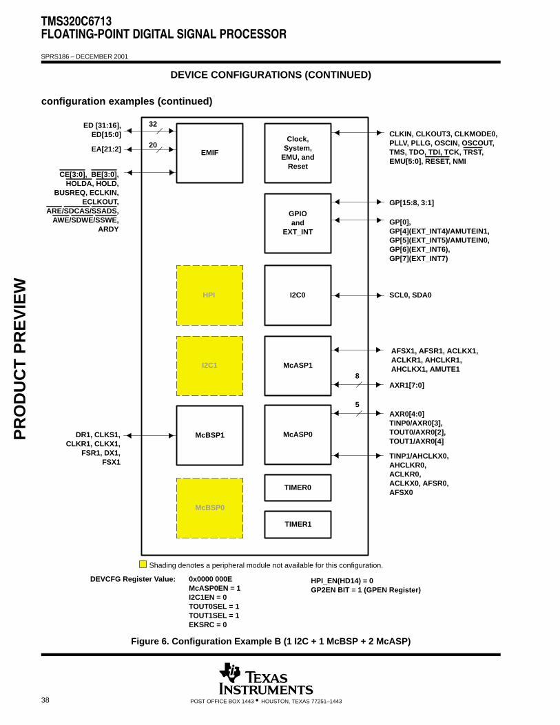
TMS320C6713FLOATING-POINT DIGITAL SIGNAL PROCESSOR
SPRS186 – DECEMBER 2001
38 POST OFFICE BOX 1443 • HOUSTON, TEXAS 77251–1443
DEVICE CONFIGURATIONS (CONTINUED)
configuration examples (continued)
EMIF
ED [31:16],ED[15:0]
CE[3:0], BE[3:0],HOLDA, HOLD,
BUSREQ, ECLKIN,ECLKOUT,
ARE/SDCAS/SSADS,AWE/SDWE/SSWE,
ARDY
HPI
I2C1
McBSP1
McBSP0
TIMER1
TIMER0
Clock,System,
EMU, andReset
I2C0
GPIOand
EXT_INT
McASP1
CLKIN, CLKOUT3, CLKMODE0,PLLV, PLLG, OSCIN, OSCOUT,TMS, TDO, TDI, TCK, TRST,EMU[5:0], RESET, NMI
GP[0],GP[4](EXT_INT4)/AMUTEIN1,GP[5](EXT_INT5)/AMUTEIN0,GP[6](EXT_INT6),GP[7](EXT_INT7)
GP[15:8, 3:1]
McASP0
SCL0, SDA0
AFSX1, AFSR1, ACLKX1,ACLKR1, AHCLKR1,AHCLKX1, AMUTE1
32
20
8
DEVCFG Register Value: 0x0000 000EMcASP0EN = 1I2C1EN = 0TOUT0SEL = 1TOUT1SEL = 1EKSRC = 0
HPI_EN(HD14) = 0GP2EN BIT = 1 (GPEN Register)
EA[21:2]
Shading denotes a peripheral module not available for this configuration.
DR1, CLKS1,CLKR1, CLKX1,
FSR1, DX1,FSX1
5
AXR1[7:0]
AXR0[4:0]TINP0/AXR0[3],TOUT0/AXR0[2],TOUT1/AXR0[4]
TINP1/AHCLKX0,AHCLKR0,ACLKR0,ACLKX0, AFSR0,AFSX0
Figure 6. Configuration Example B (1 I2C + 1 McBSP + 2 McASP)
PR
OD
UC
T P
RE
VIE
W

TMS320C6713FLOATING-POINT DIGITAL SIGNAL PROCESSOR
SPRS186 – DECEMBER 2001
39POST OFFICE BOX 1443 • HOUSTON, TEXAS 77251–1443
DEVICE CONFIGURATIONS (CONTINUED)
configuration examples (continued)
EMIF
ED [31:16],ED[15:0]
CE[3:0], BE[3:0],HOLDA, HOLD,
BUSREQ, ECLKIN,ECLKOUT,
ARE/SDCAS/SSADS,AWE/SDWE/SSWE,
ARDY
HPI
I2C1
McBSP1
SCL1, SDA1
McBSP0
TIMER1
TIMER0
Clock,System,
EMU, andReset
I2C0
GPIOand
EXT_INT
McASP1
CLKIN, CLKOUT3, CLKMODE0,PLLV, PLLG, OSCIN, OSCOUT,TMS, TDO, TDI, TCK, TRST,EMU[5:0], RESET, NMI
GP[0],GP[4](EXT_INT4)/AMUTEIN1,GP[5](EXT_INT5)/AMUTEIN0,GP[6](EXT_INT6),GP[7](EXT_INT7)
GP[15:8, 3:1]
McASP0(DIT Mode)
SCL0, SDA0
AFSX1, AFSR1, ACLKX1,ACLKR1, AHCLKR1,AHCLKX1, AMUTE1
32
20
8
DEVCFG Register Value: 0x0000 000DMcASP0EN = 0I2C1EN = 1TOUT0SEL = 1TOUT1SEL = 1EKSRC = 0
HPI_EN(HD14) = 0GP2EN BIT = 1 (GPEN Register)
EA[21:2]
Shading denotes a peripheral module not available for this configuration.
DR0, CLKS0,CLKR0, CLKX0,
FSR0, DX0,FSX0
6
AXR1[7:0]
AXR0[7:2]TINP0/AXR0[3],TOUT0/AXR0[2],TOUT1/AXR0[4]
AMUTE0,TINP1/AHCLKX0
Figure 7. Configuration Example C [2 I2C + 1 McBSP + 1 McASP + 1 McASP (DIT)]
PR
OD
UC
T P
RE
VIE
W

TMS320C6713FLOATING-POINT DIGITAL SIGNAL PROCESSOR
SPRS186 – DECEMBER 2001
40 POST OFFICE BOX 1443 • HOUSTON, TEXAS 77251–1443
DEVICE CONFIGURATIONS (CONTINUED)
configuration examples (continued)
EMIF
ED [31:16],ED[15:0]
CE[3:0], BE[3:0],HOLDA, HOLD,
BUSREQ, ECLKIN,ECLKOUT,
ARE/SDCAS/SSADS,AWE/SDWE/SSWE,
ARDY
HPI
I2C1
McBSP1DR1, CLKS1,
CLKR1, CLKX1,FSR1, DX1,
FSX1
McBSP0
TIMER1
TIMER0
Clock,System,
EMU, andReset
I2C0
GPIOand
EXT_INT
McASP1
CLKIN, CLKOUT3, CLKMODE0,PLLV, PLLG, OSCIN, OSCOUT,TMS, TDO, TDI, TCK, TRST,EMU[5:0], RESET, NMI
GP[0],GP[4](EXT_INT4)/AMUTEIN1,GP[5](EXT_INT5)/AMUTEIN0,GP[6](EXT_INT6),GP[7](EXT_INT7)
GP[15:8, 3:1]
McASP0(DIT Mode)
SCL0, SDA0
AFSX1, AFSR1, ACLKX1,ACLKR1, AHCLKR1,AHCLKX1, AMUTE1
32
20
8
DEVCFG Register Value: 0x0000 000CMcASP0EN = 0I2C1EN = 0TOUT0SEL = 1TOUT1SEL = 1EKSRC = 0
HPI_EN(HD14) = 0GP2EN BIT = 1 (GPEN Register)
EA[21:2]
Shading denotes a peripheral module not available for this configuration.
DR0, CLKS0,CLKR0, CLKX0,
FSR0, DX0,FSX0
3
AXR1[7:0]
AXR0[4:2]TINP0/AXR0[3],TOUT0/AXR0[2],TOUT1/AXR0[4]
TINP1/AHCLKX0
Figure 8. Configuration Example D [1 I2C + 2 McBSP + 1 McASP + 1 McASP (DIT)]
PR
OD
UC
T P
RE
VIE
W

TMS320C6713FLOATING-POINT DIGITAL SIGNAL PROCESSOR
SPRS186 – DECEMBER 2001
41POST OFFICE BOX 1443 • HOUSTON, TEXAS 77251–1443
DEVICE CONFIGURATIONS (CONTINUED)
configuration examples (continued)
EMIF
ED [31:16],ED[15:0]
CE[3:0], BE[3:0],HOLDA, HOLD,
BUSREQ, ECLKIN,ECLKOUT,
ARE/SDCAS/SSADS,AWE/SDWE/SSWE,
ARDY
HPI
I2C1
McBSP1
SCL1, SDA1
McBSP0
TIMER1
TIMER0
Clock,System,
EMU, andReset
GPIOand
EXT_INT
McASP1
CLKIN, CLKOUT3, CLKMODE0,PLLV, PLLG, OSCIN, OSCOUT,TMS, TDO, TDI, TCK, TRST,EMU[5:0], RESET, NMI
GP[4](EXT_INT4)/AMUTEIN1,GP[5](EXT_INT5)/AMUTEIN0,GP[6](EXT_INT6),GP[7](EXT_INT7)
McASP0
AXR0[7:0],TINP0/AXR0[3],TOUT0/AXR0[2],TOUT1/AXR0[4]
32
20
8
DEVCFG Register Value: 0x0000 000FMcASP0EN = 1I2C1EN = 1TOUT0SEL = 1TOUT1SEL = 1EKSRC = 0
HPI_EN(HD14) = 1GP2EN BIT = 0 (GPEN Register)
EA[21:2]
Shading denotes a peripheral module not available for this configuration.
CLKOUT2
HD[15:0]16
HINT, HHWIL,HRDY, HR/W,
HCNTRL1,HCNTRL0, HCS,
HDS2, HDS1,HAS
I2C0
AMUTE0,TINP1/AHCLKX0,AHCLKR0,ACLKR0,ACLKX0, AFSR0,AFSX0
Figure 9. Configuration Example E (1 I2C + HPI + 1 McASP)
PR
OD
UC
T P
RE
VIE
W

TMS320C6713FLOATING-POINT DIGITAL SIGNAL PROCESSOR
SPRS186 – DECEMBER 2001
42 POST OFFICE BOX 1443 • HOUSTON, TEXAS 77251–1443
DEVICE CONFIGURATIONS (CONTINUED)
configuration examples (continued)
EMIF
ED [31:16],ED[15:0]
CE[3:0], BE[3:0],HOLDA, HOLD,
BUSREQ, ECLKIN,ECLKOUT,
ARE/SDCAS/SSADS,AWE/SDWE/SSWE,
ARDY
HPI
I2C1
McBSP1
McBSP0
TIMER1
TIMER0
Clock,System,
EMU, andReset
GPIOand
EXT_INT
McASP1
CLKIN, CLKOUT3, CLKMODE0,PLLV, PLLG, OSCIN, OSCOUT,TMS, TDO, TDI, TCK, TRST,EMU[5:0], RESET, NMI
GP[4](EXT_INT4)/AMUTEIN1,GP[5](EXT_INT5)/AMUTEIN0,GP[6](EXT_INT6),GP[7](EXT_INT7)
McASP0
32
20
5
DEVCFG Register Value: 0x0000 000EMcASP0EN = 1I2C1EN = 1TOUT0SEL = 1TOUT1SEL = 1EKSRC = 0
HPI_EN(HD14) = 1GP2EN BIT = 0 (GPEN Register)
EA[21:2]
Shading denotes a peripheral module not available for this configuration.
DR1, CLKS1,CLKR1, CLKX1,
FSR1, DX1,FSX1
CLKOUT2
HD[15:0]16
HINT, HHWIL,HRDY, HR/W,
HCNTRL1,HCNTRL0, HCS,
HDS2, HDS1,HAS
AXR0[4:0]TINP0/AXR0[3],TOUT0/AXR0[2],TOUT1/AXR0[4]
I2C0
TINP1/AHCLKX0,AHCLKR0,ACLKR0,ACLKX0, AFSR0,AFSX0
Figure 10. Configuration Example F (1 McBSP + HPI + 1 McASP)
PR
OD
UC
T P
RE
VIE
W

TMS320C6713FLOATING-POINT DIGITAL SIGNAL PROCESSOR
SPRS186 – DECEMBER 2001
43POST OFFICE BOX 1443 • HOUSTON, TEXAS 77251–1443
DEVICE CONFIGURATIONS (CONTINUED)
debugging considerations
It is recommended that external connections be provided to peripheral selection/device configuration pins,including HD[14:12, 8, 4, 3], and CLKMODE0. Although internal pullup resistors exist on these pins, providingexternal connectivity adds convenience to the user in debugging and flexibility in switching operating modes.
Internal pullup/pulldown resistors also exist on the non-configuration pins on the HPI data bus (HD[15, 13, 11:9,7:5, 2:0]). For proper device operation, do not oppose the internal pullup/pulldown resistors on thesenon-configuration pins with external pullup/pulldown resistors. If an external controller provides signals to thesenon-configuration pins, these signals must be driven to the default state of the pins at reset, or not be drivenat all.
For the internal pullup/pulldown resistors for all device pins, see the terminal functions table.
PR
OD
UC
T P
RE
VIE
W

TMS320C6713FLOATING-POINT DIGITAL SIGNAL PROCESSOR
SPRS186 – DECEMBER 2001
44 POST OFFICE BOX 1443 • HOUSTON, TEXAS 77251–1443
TERMINAL FUNCTIONS
The terminal functions table identifies the external signal names, the associated pin (ball) numbers along withthe mechanical package designator, the pin type (I, O/Z, or I/O/Z), whether the pin has any internalpullup/pulldown resistors and a functional pin description. For more detailed information on deviceconfiguration, peripheral selection, multiplexed/shared pins, and debugging considerations, see the DeviceConfigurations section of this data sheet.
PR
OD
UC
T P
RE
VIE
W

TMS320C6713FLOATING-POINT DIGITAL SIGNAL PROCESSOR
SPRS186 – DECEMBER 2001
45POST OFFICE BOX 1443 • HOUSTON, TEXAS 77251–1443
Terminal Functions
SIGNAL PIN NO.TYPE† IPD/
‡ DESCRIPTIONNAME PYP GFN TYPE† IPD/
IPU‡ DESCRIPTION
CLOCK/PLL CONFIGURATION
CLKIN A3 I IPD Clock Input
CLKOUT2/GP[2] Y12 O/Z IPDClock output at half of device speed (O/Z) [default] (SYSCLK2 internal signal from the clock generator) or this pin can be programmed as GP[2] pin (I/O/Z)
CLKOUT3 D10 I IPD Programmable clock output (OSC Divider internal signal from clock generator)
CLKMODE0 C4 I IPUClock generator input clock source select
0 – Oscillator pads (OSCIN, OSCOUT directly from the crystal oscillator)1 – CLKIN square wave [default]
PLLV A4 A§ Analog power (1.2 V) for PLL
PLLG C6 A§ Analog ground for PLL
OSCIN D12 I — Crystal oscillator Input (XI)
OSCOUT C12 O — Crystal oscillator output (XO)
JTAG EMULATION
TMS B7 I IPU JTAG test-port mode select
TDO A8 O/Z IPU JTAG test-port data out
TDI A7 I IPU JTAG test-port data in
TCK A6 I IPU JTAG test-port clock
TRST B6 I IPD JTAG test-port reset
EMU5 — B12 I/O/Z IPU Emulation pin 5. Reserved for future use, leave unconnected.
EMU4 — C11 I/O/Z IPU Emulation pin 4. Reserved for future use, leave unconnected.
EMU3 — B10 I/O/Z IPU Emulation pin 3. Reserved for future use, leave unconnected.
EMU2 — D3 I/O/Z IPU Emulation pin 2. Reserved for future use, leave unconnected.
EMU1 B9 I/O/Z IPU Emulation pin 1¶
EMU0 D9 I/O/Z IPU Emulation pin 0¶
RESETS AND INTERRUPTS
RESET A13 I IPU Device reset
NMI C13 I IPDNonmaskable interrupt• Edge-driven (rising edge)
GP[7](EXT_INT7) E3 General-purpose input/output pins (I/O/Z) which also function as external interrupts [default]
GP[6](EXT_INT6) D2interrupts [default]• Edge-driven
Polarity independently selected via the External Interrupt Polarity RegisterGP[5](EXT_INT5)/AMUTEIN0
C1 I/O/Z IPU• Polarity independently selected via the External Interrupt Polarity Register
bits (EXTPOL.[3:0])
GP[4] d GP[5] i l f ti AMUTEIN1 M ASP1 t i t dGP[4](EXT_INT4)/AMUTEIN1
C2
GP[4] and GP[5] pins also function as AMUTEIN1 McASP1 mute input and AMUTEIN0 McASP0 mute input, respectively, if enabled by the INSTAT bit in theMcASP AMUTE register.
† I = Input, O = Output, Z = High impedance, S = Supply voltage, GND = Ground‡ IPD = Internal pulldown, IPU = Internal pullup. (These IPD/IPU signal pins feature a 30-kΩ IPD or IPU resistor. To pull up a signal to the opposite
supply rail, a 1-kΩ resistor should be used.)§ A = Analog signal (PLL Filter)¶ The EMU0 and EMU1 pins are internally pulled up with 30-kΩ resistors; therefore, for emulation and normal operation, no external
pullup/pulldown resistors are necessary. However, for boundary scan operation, pull down the EMU1 and EMU0 pins with a dedicated 1-kΩresistor.
PR
OD
UC
T P
RE
VIE
W
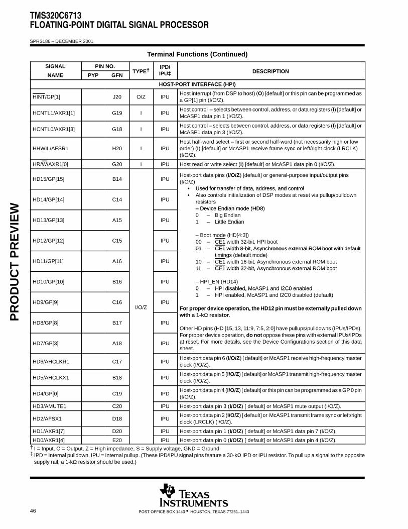
TMS320C6713FLOATING-POINT DIGITAL SIGNAL PROCESSOR
SPRS186 – DECEMBER 2001
46 POST OFFICE BOX 1443 • HOUSTON, TEXAS 77251–1443
Terminal Functions (Continued)
SIGNAL PIN NO.TYPE†
IPD/DESCRIPTION
NAME PYP GFNTYPE†
IPD/IPU‡ DESCRIPTION
HOST-PORT INTERFACE (HPI)
HINT/GP[1] J20 O/Z IPUHost interrupt (from DSP to host) (O) [default] or this pin can be programmed asa GP[1] pin (I/O/Z).
HCNTL1/AXR1[1] G19 I IPUHost control – selects between control, address, or data registers (I) [default] orMcASP1 data pin 1 (I/O/Z).
HCNTL0/AXR1[3] G18 I IPUHost control – selects between control, address, or data registers (I) [default] orMcASP1 data pin 3 (I/O/Z).
HHWIL/AFSR1 H20 I IPUHost half-word select – first or second half-word (not necessarily high or low order) (I) [default] or McASP1 receive frame sync or left/right clock (LRCLK)(I/O/Z).
HR/W/AXR1[0] G20 I IPU Host read or write select (I) [default] or McASP1 data pin 0 (I/O/Z).
HD15/GP[15] B14 IPUHost-port data pins (I/O/Z) [default] or general-purpose input/output pins(I/O/Z)
• Used for transfer of data address and control
HD14/GP[14] C14 IPU
• Used for transfer of data, address, and control• Also controls initialization of DSP modes at reset via pullup/pulldown
resistors– Device Endian mode (HD8)
HD13/GP[13] A15 IPU
– Device Endian mode (HD8)0 – Big Endian1 – Little Endian
HD12/GP[12] C15 IPU– Boot mode (HD[4:3])00 – CE1 width 32-bit, HPI boot 01 – CE1 width 8-bit, Asynchronous external ROM boot with default
HD11/GP[11] A16 IPU
01 – CE1 width 8-bit, Asynchronous external ROM boot with default timings (default mode)
10 – CE1 width 16-bit, Asynchronous external ROM boot 11 – CE1 width 32-bit, Asynchronous external ROM boot
HD10/GP[10] B16 IPU
11 CE1 width 32-bit, Asynchronous external ROM boot
– HPI_EN (HD14)0 – HPI disabled, McASP1 and I2C0 enabled
HD9/GP[9] C16I/O/Z
IPU
0 HPI disabled, McASP1 and I2C0 enabled1 – HPI enabled, McASP1 and I2C0 disabled (default)
For proper device operation, the HD12 pin must be externally pulled down
HD8/GP[8] B17 IPU
For proper device operation, the HD12 pin must be externally pulled downwith a 1-kΩ resistor.
Other HD pins (HD [15, 13, 11:9, 7:5, 2:0] have pullups/pulldowns (IPUs/IPDs).
HD7/GP[3] A18 IPU
( [ , , , , ] ( )For proper device operation, do not oppose these pins with external IPUs/IPDsat reset. For more details, see the Device Configurations section of this datasheet.
HD6/AHCLKR1 C17 IPUHost-port data pin 6 (I/O/Z) [ default] or McASP1 receive high-frequency masterclock (I/O/Z).
HD5/AHCLKX1 B18 IPUHost-port data pin 5 (I/O/Z) [ default] or McASP1 transmit high-frequency masterclock (I/O/Z).
HD4/GP[0] C19 IPDHost-port data pin 4 (I/O/Z) [ default] or this pin can be programmed as a GP 0 pin(I/O/Z).
HD3/AMUTE1 C20 IPU Host-port data pin 3 (I/O/Z) [ default] or McASP1 mute output (I/O/Z).
HD2/AFSX1 D18 IPUHost-port data pin 2 (I/O/Z) [ default] or McASP1 transmit frame sync or left/rightclock (LRCLK) (I/O/Z).
HD1/AXR1[7] D20 IPU Host-port data pin 1 (I/O/Z) [ default] or McASP1 data pin 7 (I/O/Z).
HD0/AXR1[4] E20 IPU Host-port data pin 0 (I/O/Z) [ default] or McASP1 data pin 4 (I/O/Z).† I = Input, O = Output, Z = High impedance, S = Supply voltage, GND = Ground‡ IPD = Internal pulldown, IPU = Internal pullup. (These IPD/IPU signal pins feature a 30-kΩ IPD or IPU resistor. To pull up a signal to the opposite
supply rail, a 1-kΩ resistor should be used.)
PR
OD
UC
T P
RE
VIE
W
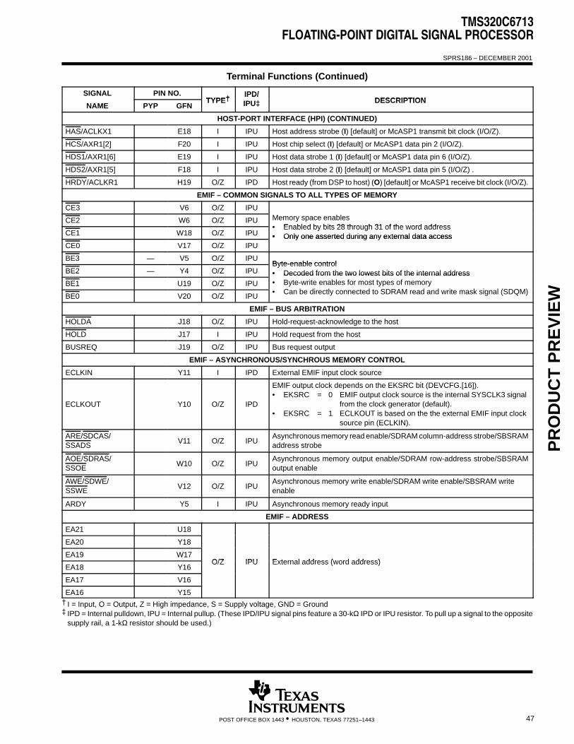
TMS320C6713FLOATING-POINT DIGITAL SIGNAL PROCESSOR
SPRS186 – DECEMBER 2001
47POST OFFICE BOX 1443 • HOUSTON, TEXAS 77251–1443
Terminal Functions (Continued)
SIGNAL PIN NO.TYPE†
IPD/DESCRIPTION
NAME PYP GFNTYPE†
IPD/IPU‡ DESCRIPTION
HOST-PORT INTERFACE (HPI) (CONTINUED)
HAS/ACLKX1 E18 I IPU Host address strobe (I) [default] or McASP1 transmit bit clock (I/O/Z).
HCS/AXR1[2] F20 I IPU Host chip select (I) [default] or McASP1 data pin 2 (I/O/Z).
HDS1/AXR1[6] E19 I IPU Host data strobe 1 (I) [default] or McASP1 data pin 6 (I/O/Z).
HDS2/AXR1[5] F18 I IPU Host data strobe 2 (I) [default] or McASP1 data pin 5 (I/O/Z) .
HRDY/ACLKR1 H19 O/Z IPD Host ready (from DSP to host) (O) [default] or McASP1 receive bit clock (I/O/Z).
EMIF – COMMON SIGNALS TO ALL TYPES OF MEMORY
CE3 V6 O/Z IPU
CE2 W6 O/Z IPU Memory space enables• Enabled by bits 28 through 31 of the word address
CE1 W18 O/Z IPU• Enabled by bits 28 through 31 of the word address• Only one asserted during any external data access
CE0 V17 O/Z IPU• Only one asserted during any external data access
BE3 — V5 O/Z IPUByte-enable control
BE2 — Y4 O/Z IPUByte-enable control• Decoded from the two lowest bits of the internal address
BE1 U19 O/Z IPU• Decoded from the two lowest bits of the internal address• Byte-write enables for most types of memory
C b di tl t d t SDRAM d d it k i l (SDQM)BE0 V20 O/Z IPU
y y y• Can be directly connected to SDRAM read and write mask signal (SDQM)
EMIF – BUS ARBITRATION
HOLDA J18 O/Z IPU Hold-request-acknowledge to the host
HOLD J17 I IPU Hold request from the host
BUSREQ J19 O/Z IPU Bus request output
EMIF – ASYNCHRONOUS/SYNCHROUS MEMORY CONTROL
ECLKIN Y11 I IPD External EMIF input clock source
ECLKOUT Y10 O/Z IPD
EMIF output clock depends on the EKSRC bit (DEVCFG.[16]).• EKSRC = 0 EMIF output clock source is the internal SYSCLK3 signal
from the clock generator (default).• EKSRC = 1 ECLKOUT is based on the the external EMIF input clock
source pin (ECLKIN).
ARE/SDCAS/SSADS
V11 O/Z IPUAsynchronous memory read enable/SDRAM column-address strobe/SBSRAMaddress strobe
AOE/SDRAS/SSOE
W10 O/Z IPUAsynchronous memory output enable/SDRAM row-address strobe/SBSRAMoutput enable
AWE/SDWE/SSWE
V12 O/Z IPUAsynchronous memory write enable/SDRAM write enable/SBSRAM writeenable
ARDY Y5 I IPU Asynchronous memory ready input
EMIF – ADDRESS
EA21 U18
EA20 Y18
EA19 W17O/Z IPU External address (word address)
EA18 Y16O/Z IPU External address (word address)
EA17 V16
EA16 Y15† I = Input, O = Output, Z = High impedance, S = Supply voltage, GND = Ground‡ IPD = Internal pulldown, IPU = Internal pullup. (These IPD/IPU signal pins feature a 30-kΩ IPD or IPU resistor. To pull up a signal to the opposite
supply rail, a 1-kΩ resistor should be used.)
PR
OD
UC
T P
RE
VIE
W

TMS320C6713FLOATING-POINT DIGITAL SIGNAL PROCESSOR
SPRS186 – DECEMBER 2001
48 POST OFFICE BOX 1443 • HOUSTON, TEXAS 77251–1443
Terminal Functions (Continued)
SIGNAL PIN NO.TYPE† IPD/
DESCRIPTIONNAME PYP GFN
TYPE† IPD/IPU‡ DESCRIPTION
EMIF – ADDRESS (CONTINUED)
EA15 W15
EA14 Y14
EA13 W14
EA12 V14
EA11 W13
EA10 V10
EA9 Y9O/Z IPU External address (word address)
EA8 V9O/Z IPU External address (word address)
EA7 Y8
EA6 W8
EA5 V8
EA4 W7
EA3 V7
EA2 Y6
EMIF – DATA
ED31 N3
ED30 P3
ED29 P2
ED28 P1
ED27 R2
ED26 R3
ED25 T2
ED24 T1
ED23 U3
ED22 U1
ED21 U2
ED20 V1I/O/Z IPU External data pins (ED[31:16] pins applicable to GFN package only)
ED19 V2I/O/Z IPU External data pins (ED[31:16] pins applicable to GFN package only)
ED18 Y3
ED17 W4
ED16 V4
ED15 T19
ED14 T20
ED13 T18
ED12 R20
ED11 R19
ED10 P20
ED9 P18
ED8 N20† I = Input, O = Output, Z = High impedance, S = Supply voltage, GND = Ground‡ IPD = Internal pulldown, IPU = Internal pullup. (These IPD/IPU signal pins feature a 30-kΩ IPD or IPU resistor. To pull up a signal to the opposite
supply rail, a 1-kΩ resistor should be used.)
PR
OD
UC
T P
RE
VIE
W
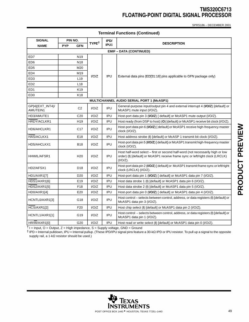
TMS320C6713FLOATING-POINT DIGITAL SIGNAL PROCESSOR
SPRS186 – DECEMBER 2001
49POST OFFICE BOX 1443 • HOUSTON, TEXAS 77251–1443
Terminal Functions (Continued)
SIGNAL PIN NO.TYPE†
IPD/DESCRIPTION
NAME PYP GFNTYPE†
IPD/IPU‡ DESCRIPTION
EMIF – DATA (CONTINUED)
ED7 N19
ED6 N18
ED5 M20
ED4 M19I/O/Z IPU External data pins (ED[31:16] pins applicable to GFN package only)
ED3 L19I/O/Z IPU External data pins (ED[31:16] pins applicable to GFN package only)
ED2 L18
ED1 K19
ED0 K18
MULTICHANNEL AUDIO SERIAL PORT 1 (McASP1)
GP[4](EXT_INT4)/AMUTEIN1
C2 I/O/Z IPUGeneral-purpose input/output pin 4 and external interrupt 4 (I/O/Z) [default] orMcASP1 mute input (I/O/Z).
HD3/AMUTE1 C20 I/O/Z IPU Host-port data pin 3 (I/O/Z) [ default] or McASP1 mute output (I/O/Z).
HRDY/ACLKR1 H19 I/O/Z IPU Host ready (from DSP to host) (O) [default] or McASP1 receive bit clock (I/O/Z).
HD6/AHCLKR1 C17 I/O/Z IPUHost-port data pin 6 (I/O/Z) [ default] or McASP1 receive high-frequency masterclock (I/O/Z).
HAS/ACLKX1 E18 I/O/Z IPU Host address strobe (I) [default] or McASP 1 transmit bit clock (I/O/Z).
HD5/AHCLKX1 B18 I/O/Z IPUHost-port data pin 5 (I/O/Z) [ default] or McASP1 transmit high-frequency masterclock (I/O/Z).
HHWIL/AFSR1 H20 I/O/Z IPUHost half-word select – first or second half-word (not necessarily high or low order) (I) [default] or McASP1 receive frame sync or left/right clock (LRCLK)(I/O/Z).
HD2/AFSX1 D18 I/O/Z IPUHost-port data pin 2 (I/O/Z) [ default] or McASP1 transmit frame sync or left/rightclock (LRCLK) (I/O/Z).
HD1/AXR1[7] D20 I/O/Z IPU Host-port data pin 1 (I/O/Z) [ default] or McASP1 data pin 7 (I/O/Z).
HDS1/AXR1[6] E19 I/O/Z IPU Host data strobe 1 (I) [default] or McASP1 data pin 6 (I/O/Z).
HDS2/AXR1[5] F18 I/O/Z IPU Host data strobe 2 (I) [default] or McASP1 data pin 5 (I/O/Z).
HD0/AXR1[4] E20 I/O/Z IPU Host-port data pin 0 (I/O/Z) [ default] or McASP1 data pin 4 (I/O/Z).
HCNTL0/AXR1[3] G18 I/O/Z IPUHost control – selects between control, address, or data registers (I) [default] orMcASP1 data pin 3 (I/O/Z).
HCS/AXR1[2] F20 I/O/Z IPU Host chip select (I) [default] or McASP1 data pin 2 (I/O/Z).
HCNTL1/AXR1[1] G19 I/O/Z IPUHost control – selects between control, address, or data registers (I) [default] orMcASP1 data pin 1 (I/O/Z).
HR/W/AXR1[0] G20 I/O/Z IPU Host read or write select (I) [default] or McASP1 data pin 0 (I/O/Z).† I = Input, O = Output, Z = High impedance, S = Supply voltage, GND = Ground‡ IPD = Internal pulldown, IPU = Internal pullup. (These IPD/IPU signal pins feature a 30-kΩ IPD or IPU resistor. To pull up a signal to the opposite
supply rail, a 1-kΩ resistor should be used.)
PR
OD
UC
T P
RE
VIE
W
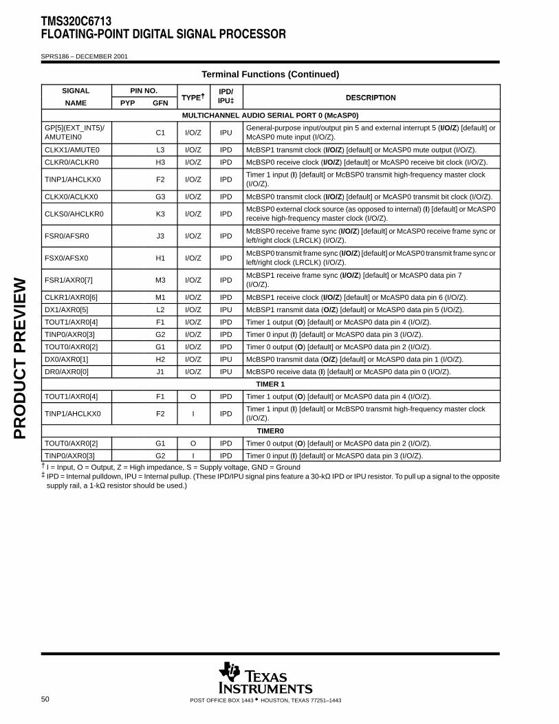
TMS320C6713FLOATING-POINT DIGITAL SIGNAL PROCESSOR
SPRS186 – DECEMBER 2001
50 POST OFFICE BOX 1443 • HOUSTON, TEXAS 77251–1443
Terminal Functions (Continued)
SIGNAL PIN NO.TYPE†
IPD/DESCRIPTION
NAME PYP GFNTYPE†
IPD/IPU‡ DESCRIPTION
MULTICHANNEL AUDIO SERIAL PORT 0 (McASP0)
GP[5](EXT_INT5)/AMUTEIN0
C1 I/O/Z IPUGeneral-purpose input/output pin 5 and external interrupt 5 (I/O/Z) [default] orMcASP0 mute input (I/O/Z).
CLKX1/AMUTE0 L3 I/O/Z IPD McBSP1 transmit clock (I/O/Z) [default] or McASP0 mute output (I/O/Z).
CLKR0/ACLKR0 H3 I/O/Z IPD McBSP0 receive clock (I/O/Z) [default] or McASP0 receive bit clock (I/O/Z).
TINP1/AHCLKX0 F2 I/O/Z IPDTimer 1 input (I) [default] or McBSP0 transmit high-frequency master clock(I/O/Z).
CLKX0/ACLKX0 G3 I/O/Z IPD McBSP0 transmit clock (I/O/Z) [default] or McASP0 transmit bit clock (I/O/Z).
CLKS0/AHCLKR0 K3 I/O/Z IPDMcBSP0 external clock source (as opposed to internal) (I) [default] or McASP0receive high-frequency master clock (I/O/Z).
FSR0/AFSR0 J3 I/O/Z IPDMcBSP0 receive frame sync (I/O/Z) [default] or McASP0 receive frame sync orleft/right clock (LRCLK) (I/O/Z).
FSX0/AFSX0 H1 I/O/Z IPDMcBSP0 transmit frame sync (I/O/Z) [default] or McASP0 transmit frame sync orleft/right clock (LRCLK) (I/O/Z).
FSR1/AXR0[7] M3 I/O/Z IPDMcBSP1 receive frame sync (I/O/Z) [default] or McASP0 data pin 7 (I/O/Z).
CLKR1/AXR0[6] M1 I/O/Z IPD McBSP1 receive clock (I/O/Z) [default] or McASP0 data pin 6 (I/O/Z).
DX1/AXR0[5] L2 I/O/Z IPU McBSP1 rransmit data (O/Z) [default] or McASP0 data pin 5 (I/O/Z).
TOUT1/AXR0[4] F1 I/O/Z IPD Timer 1 output (O) [default] or McASP0 data pin 4 (I/O/Z).
TINP0/AXR0[3] G2 I/O/Z IPD Timer 0 input (I) [default] or McASP0 data pin 3 (I/O/Z).
TOUT0/AXR0[2] G1 I/O/Z IPD Timer 0 output (O) [default] or McASP0 data pin 2 (I/O/Z).
DX0/AXR0[1] H2 I/O/Z IPU McBSP0 transmit data (O/Z) [default] or McASP0 data pin 1 (I/O/Z).
DR0/AXR0[0] J1 I/O/Z IPU McBSP0 receive data (I) [default] or McASP0 data pin 0 (I/O/Z).
TIMER 1
TOUT1/AXR0[4] F1 O IPD Timer 1 output (O) [default] or McASP0 data pin 4 (I/O/Z).
TINP1/AHCLKX0 F2 I IPDTimer 1 input (I) [default] or McBSP0 transmit high-frequency master clock(I/O/Z).
TIMER0
TOUT0/AXR0[2] G1 O IPD Timer 0 output (O) [default] or McASP0 data pin 2 (I/O/Z).
TINP0/AXR0[3] G2 I IPD Timer 0 input (I) [default] or McASP0 data pin 3 (I/O/Z).† I = Input, O = Output, Z = High impedance, S = Supply voltage, GND = Ground‡ IPD = Internal pulldown, IPU = Internal pullup. (These IPD/IPU signal pins feature a 30-kΩ IPD or IPU resistor. To pull up a signal to the opposite
supply rail, a 1-kΩ resistor should be used.)
PR
OD
UC
T P
RE
VIE
W

TMS320C6713FLOATING-POINT DIGITAL SIGNAL PROCESSOR
SPRS186 – DECEMBER 2001
51POST OFFICE BOX 1443 • HOUSTON, TEXAS 77251–1443
Terminal Functions (Continued)
SIGNAL PIN NO.TYPE†
IPD/DESCRIPTION
NAME PYP GFNTYPE†
IPD/IPU‡ DESCRIPTION
MULTICHANNEL BUFFERED SERIAL PORT 1 (McBSP1)
CLKS1/SCL1 E1 I IPDMcBSP1 external clock source (as opposed to internal) (I) [default] or I2C1 clock(I/O/Z).
CLKR1/AXR0[6] M1 I/O/Z IPD McBSP1 receive clock (I/O/Z) [default] or McASP0 TX/RX data pin 6 (I/O/Z).
CLKX1/AMUTE0 L3 I/O/Z IPD McBSP1 transmit clock (I/O/Z) [default] or McASP0 mute output (I/O/Z).
DR1/SDA1 M2 I IPU McBSP1 receive data (I) [default] or I2C1 data (I/O/Z).
DX1/AXR0[5] L2 O/Z IPU McBSP1 transmit data (O/Z) [default] or McASP0 TX/RX data pin 5 (I/O/Z).
FSR1/AXR0[7] M3 I/O/Z IPDMcBSP1 receive frame sync (I/O/Z) [default] or McASP0 TX/RX data pin 7 (I/O/Z).
FSX1 L1 I/O/Z IPD McBSP1 transmit frame sync
MULTICHANNEL BUFFERED SERIAL PORT 0 (McBSP0)
CLKS0/AHCLKR0 K3 I IPDMcBSP0 external clock source (as opposed to internal) (I) [default] or McASP0receive high-frequency master clock (I/O/Z).
CLKR0/ACLKR0 H3 I/O/Z IPD McBSP0 receive clock (I/O/Z) [default] or McASP0 receive bit clock (I/O/Z).
CLKX0/ACLKX0 G3 I/O/Z IPD McBSP0 transmit clock (I/O/Z) [default] or McASP0 transmit bit clock (I/O/Z).
DR0/AXR0[0] J1 I IPU McBSP0 receive data (I) [default] or McASP0 TX/RX data pin 0 (I/O/Z).
DX0/AXR0[1] H2 O/Z IPU McBSP0 transmit data (O/Z) [default] or McASP0 TX/RX data pin 1 (I/O/Z).
FSR0/AFSR0 J3 I/O/Z IPDMcBSP0 receive frame sync (I/O/Z) [default] or McASP0 receive frame sync orleft/right clock (LRCLK) (I/O/Z).
FSX0/AFSX0 H1 I/O/Z IPDMcBSP0 transmit frame sync (I/O/Z) [default] or McASP0 transmit frame sync orleft/right clock (LRCLK) (I/O/Z).
INTER-INTEGRATED CIRCUIT 1 (I2C1)
CLKS1/SCL1 E1 I/O/Z IPDMcBSP1 external clock source (as opposed to internal) (I) [default] or I2C1 clock(I/O/Z).
DR1/SDA1 M2 I/O/Z IPU McBSP1 receive data (I) [default] or I2C1 data (I/O/Z).
INTER-INTEGRATED CIRCUIT 0 (I2C0)
SCL0 N1 I/O/Z IPU I2C0 clock.
SDA0 N2 I/O/Z IPU I2C0 data.† I = Input, O = Output, Z = High impedance, S = Supply voltage, GND = Ground‡ IPD = Internal pulldown, IPU = Internal pullup. (These IPD/IPU signal pins feature a 30-kΩ IPD or IPU resistor. To pull up a signal to the opposite
supply rail, a 1-kΩ resistor should be used.)
PR
OD
UC
T P
RE
VIE
W

TMS320C6713FLOATING-POINT DIGITAL SIGNAL PROCESSOR
SPRS186 – DECEMBER 2001
52 POST OFFICE BOX 1443 • HOUSTON, TEXAS 77251–1443
Terminal Functions (Continued)
SIGNAL PIN NO.TYPE†
IPD/DESCRIPTION
NAME PYP GFNTYPE†
IPD/IPU‡ DESCRIPTION
GENERAL-PURPOSE INPUT/OUTPUT (GPIO)
HD15/GP[15] B14 IPUHost-port data pins (I/O/Z) [default] or general-purpose input/output pins(I/O/Z)
• Used for transfer of data, address, and control
HD14/GP[14] C14 IPU
• Used for transfer of data, address, and control• Also controls initialization of DSP modes at reset via pullup/pulldown
resistors– Device Endian mode (HD8)0 Big Endian
HD13/GP[13] A15 IPU
0 – Big Endian1 – Little Endian
– Boot mode (HD[4:3])
HD12/GP[12] C15
I/O/Z
IPU
– Boot mode (HD[4:3])00 – CE1 width 32-bit, HPI boot 01 – CE1 width 8-bit, Asynchronous external ROM boot with default
timings (default mode)10 CE1 width 16 bit Asynchronous external ROM boot
HD11/GP[11] A16
I/O/Z
IPU
10 – CE1 width 16-bit, Asynchronous external ROM boot 11 – CE1 width 32-bit, Asynchronous external ROM boot
– HPI_EN (HD14)
HD10/GP[10] B16 IPU
– HPI_EN (HD14)0 – HPI disabled, McASP1 and I2C0 enabled1 – HPI enabled, McASP1 and I2C0 disabled (default)
F d i ti th HD12 i t b t ll ll d d
HD9/GP[9] C16 IPU
For proper device operation, the HD12 pin must be externally pulled downwith a 1-kΩ resistor.
Other HD pins (HD [15, 13, 11:9, 7:5, 2:0] have pullups/pulldowns (IPUs/IPDs).
HD8/GP[8] B17 IPU
Other HD ins (HD [15, 13, 11:9, 7:5, 2:0] have ullu s/ ulldowns (IPUs/IPDs).For proper device operation, do not oppose these pins with external IPUs/IPDsat reset. For more details, see the Device Configurations section of this datasheet.
GP[7](EXT_INT7) E3 General-purpose input/output pins (I/O/Z) which also function as external interrupts [default]
GP[6](EXT_INT6) D2interrupts [default]• Edge-driven
Polarity independently selected via the External Interrupt Polarity RegisterGP[5](EXT_INT5)/AMUTEIN0
C1 I/O/Z IPU• Polarity independently selected via the External Interrupt Polarity Register
bits (EXTPOL.[3:0])
GP[4] d GP[5] i l f ti AMUTEIN1 M ASP1 t i t dGP[4](EXT_INT4)/AMUTEIN1
C2
GP[4] and GP[5] pins also function as AMUTEIN1 McASP1 mute input and AMUTEIN0 McASP0 mute input, respectively, if enabled by the INSTAT bit in theMcASP AMUTE register.
HD7/GP[3] A18 I/O/Z IPUHost-port data pin 7 (I/O/Z) [default] or general-purpose input/output 0 pin 3(I/O/Z)
CLKOUT2/GP[2] Y12 I/O/Z IPDClock output at half of device speed (O/Z) [default] or this pin can beprogrammed as GP[2] pin.
HINT/GP[1] J20 O IPUHost interrupt (from DSP to host) (O) [default] or this pin can be programmed asa GP[1] pin (I/O/Z).
HD4/GP[0] C19 I/O/Z IPDHost-port data pin 4 (I/O/Z) [ default] or this pin can be programmed as a GP[0]pin (I/O/Z).
RESERVED FOR TEST
RSV0 A5 O/Z IPU Reserved. (Leave unconnected, do not connect to power or ground)
RSV1 B5 A§ Reserved. (Leave unconnected, do not connect to power or ground)
RSV2 D7 O/Z IPD Reserved. (Leave unconnected, do not connect to power or ground)† I = Input, O = Output, Z = High impedance, S = Supply voltage, GND = Ground‡ IPD = Internal pulldown, IPU = Internal pullup. (These IPD/IPU signal pins feature a 30-kΩ IPD or IPU resistor. To pull up a signal to the opposite
supply rail, a 1-kΩ resistor should be used.)§ A = Analog signal
PR
OD
UC
T P
RE
VIE
W

TMS320C6713FLOATING-POINT DIGITAL SIGNAL PROCESSOR
SPRS186 – DECEMBER 2001
53POST OFFICE BOX 1443 • HOUSTON, TEXAS 77251–1443
Terminal Functions (Continued)
SIGNAL PIN NO.TYPE† DESCRIPTION
NAME PYP GFNTYPE† DESCRIPTION
SUPPLY VOLTAGE PINS
A17
B3
B8
B13
C5
C10
D1
D16
D19
F3
H18
J2
M18
DVR1
S 3 3 V supply voltageDVDD R18S 3.3-V supply voltage
T3
U5
U7
U12
U16
V13
V15
V19
W3
W9
W12
Y7
Y17
A9
A10
A12
B2
B19
CVC3
S 1 2 V supply voltageCVDD C7S 1.2-V supply voltage
C18
D5
D6
D11
D14† I = Input, O = Output, Z = High impedance, S = Supply voltage, GND = Ground
PR
OD
UC
T P
RE
VIE
W

TMS320C6713FLOATING-POINT DIGITAL SIGNAL PROCESSOR
SPRS186 – DECEMBER 2001
54 POST OFFICE BOX 1443 • HOUSTON, TEXAS 77251–1443
Terminal Functions (Continued)
SIGNAL PIN NO.TYPE† DESCRIPTION
NAME PYP GFNTYPE† DESCRIPTION
SUPPLY VOLTAGE PINS (CONTINUED)
D15
F4
F17
K1
K4
K17
L4
L17
L20
R4
R17
U6
U10
U11
U14
CVU15
S 1 2 V supply voltageCVDD V3S 1.2-V supply voltage
V18
W2
W19
—
—
—
—
—
—
—
—
—
—
—
—
GROUND PINS
A1
A2
A11
VA14
GND Ground pinsVSS A19GND Ground pins
A20
B1
B4† I = Input, O = Output, Z = High impedance, S = Supply voltage, GND = Ground
PR
OD
UC
T P
RE
VIE
W

TMS320C6713FLOATING-POINT DIGITAL SIGNAL PROCESSOR
SPRS186 – DECEMBER 2001
55POST OFFICE BOX 1443 • HOUSTON, TEXAS 77251–1443
Terminal Functions (Continued)
SIGNAL PIN NO.TYPE† DESCRIPTION
NAME PYP GFNTYPE† DESCRIPTION
GROUND PINS (CONTINUED)
B11
B15
B20
C8
C9
D4
D8
D13
D17
E2
E4
E17
F19
G4
G17
H4
H17
J4
K2
VSS K20 GND Ground pinsVSSM4
GND Ground ins
M17
N4
N17
P4
P17
P19
T4
T17
U4
U8
U9
U13
U17
U20
W1
W5
W11
W16† I = Input, O = Output, Z = High impedance, S = Supply voltage, GND = Ground
PR
OD
UC
T P
RE
VIE
W

TMS320C6713FLOATING-POINT DIGITAL SIGNAL PROCESSOR
SPRS186 – DECEMBER 2001
56 POST OFFICE BOX 1443 • HOUSTON, TEXAS 77251–1443
Terminal Functions (Continued)
SIGNAL PIN NO.TYPE† DESCRIPTION
NAME PYP GFNTYPE† DESCRIPTION
GROUND PINS (CONTINUED)
W20
Y1
Y2
Y13
Y19
Y20
—
—
V—
GND Ground pinsVSS —GND Ground pins
—
—
—
—
—
—
—
—† I = Input, O = Output, Z = High impedance, S = Supply voltage, GND = Ground
PR
OD
UC
T P
RE
VIE
W

TMS320C6713FLOATING-POINT DIGITAL SIGNAL PROCESSOR
SPRS186 – DECEMBER 2001
57POST OFFICE BOX 1443 • HOUSTON, TEXAS 77251–1443
development support
TI offers an extensive line of development tools for the TMS320C6000 DSP platform, including tools toevaluate the performance of the processors, generate code, develop algorithm implementations, and fullyintegrate and debug software and hardware modules.
The following products support development of C6000 DSP-based applications:
Software Development Tools:Code Composer Studio Integrated Development Environment (IDE): including EditorC/C++/Assembly Code Generation, and Debug plus additional development toolsScalable, Real-Time Foundation Software (DSP/BIOS ), which provides the basic run-time target softwareneeded to support any DSP application.
Hardware Development Tools:Extended Development System (XDS ) Emulator (supports C6000 DSP multiprocessor system debug)EVM (Evaluation Module)
The TMS320 DSP Development Support Reference Guide (SPRU011) contains information aboutdevelopment-support products for all TMS320 DSP family member devices, including documentation. Seethis document for further information on TMS320 DSP documentation or any TMS320 DSP support productsfrom Texas Instruments. An additional document, the TMS320 Third-Party Support Reference Guide(SPRU052), contains information about TMS320 DSP-related products from other companies in the industry.To receive TMS320 DSP literature, contact the Literature Response Center at 800/477-8924.
For a complete listing of development-support tools for the TMS320C6000 DSP platform, visit the TexasInstruments web site on the Worldwide Web at http://www.ti.com uniform resource locator (URL) and select“Find Development Tools”. For device-specific tools, under “Semiconductor Products”, select “Digital SignalProcessors”, choose a product family, and select the particular DSP device. For information on pricing andavailability, contact the nearest TI field sales office or authorized distributor.
TI offers an extensive line of development tools for the TMS320C6000 DSP platform, including tools toevaluate the performance of the processors, generate code, develop algorithm implementations, and fullyintegrate and debug software and hardware modules.
PR
OD
UC
T P
RE
VIE
W
Code Composer Studio, DSP/BIOS, XDS, and TMS320 are trademarks of Texas Instruments.

TMS320C6713FLOATING-POINT DIGITAL SIGNAL PROCESSOR
SPRS186 – DECEMBER 2001
58 POST OFFICE BOX 1443 • HOUSTON, TEXAS 77251–1443
device and development-support tool nomenclature
To designate the stages in the product development cycle, TI assigns prefixes to the part numbers of allTMS320 DSP devices and support tools. Each TMS320 DSP commercial family member has one of threeprefixes: TMX, TMP, or TMS. Texas Instruments recommends two of three possible prefix designators forsupport tools: TMDX and TMDS. These prefixes represent evolutionary stages of product development fromengineering prototypes (TMX/TMDX) through fully qualified production devices/tools (TMS/TMDS).
Device development evolutionary flow:
TMX Experimental device that is not necessarily representative of the final device’s electricalspecifications
TMP Final silicon die that conforms to the device’s electrical specifications but has not completedquality and reliability verification
TMS Fully qualified production device
Support tool development evolutionary flow:
TMDX Development-support product that has not yet completed Texas Instruments internal qualificationtesting.
TMDS Fully qualified development-support product
TMX and TMP devices and TMDX development-support tools are shipped against the following disclaimer:
“Developmental product is intended for internal evaluation purposes.”
TMS devices and TMDS development-support tools have been characterized fully, and the quality and reliabilityof the device have been demonstrated fully. TI’s standard warranty applies.
Predictions show that prototype devices (TMX or TMP) have a greater failure rate than the standard productiondevices. Texas Instruments recommends that these devices not be used in any production system because theirexpected end-use failure rate still is undefined. Only qualified production devices are to be used.
TI device nomenclature also includes a suffix with the device family name. This suffix indicates the package type(for example, GFN), the temperature range (for example, blank is the default commercial temperature range),and the device speed range in megahertz (for example, -225 is 225 MHz).
Figure 11 provides a legend for reading the complete device name for any TMS320C6000 DSP familymember.
PR
OD
UC
T P
RE
VIE
W
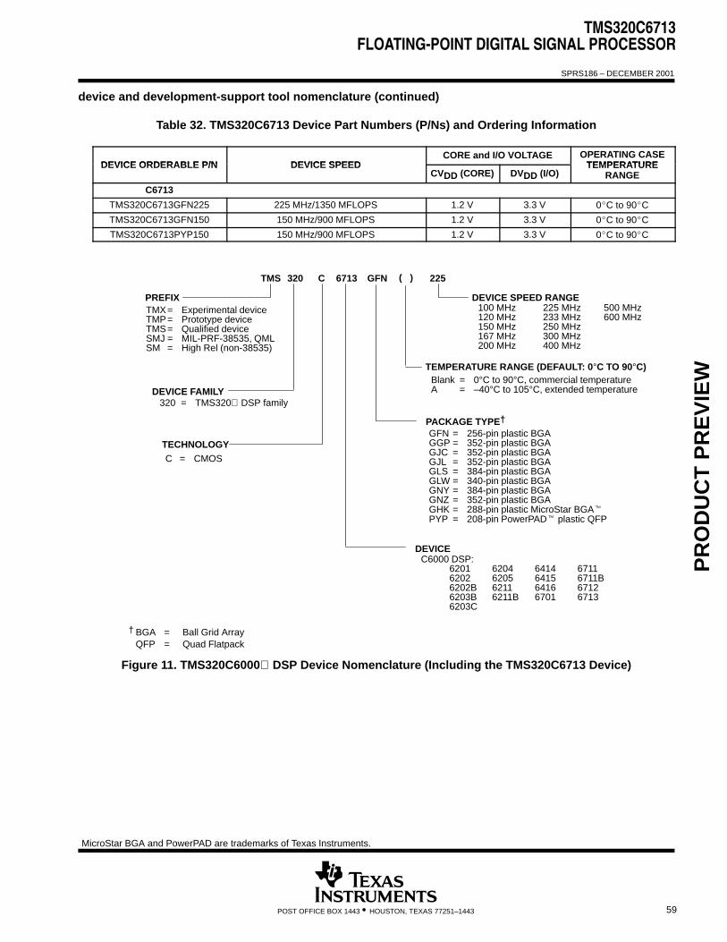
TMS320C6713FLOATING-POINT DIGITAL SIGNAL PROCESSOR
SPRS186 – DECEMBER 2001
59POST OFFICE BOX 1443 • HOUSTON, TEXAS 77251–1443
device and development-support tool nomenclature (continued)
Table 32. TMS320C6713 Device Part Numbers (P/Ns) and Ordering Information
DEVICE ORDERABLE P/N DEVICE SPEEDCORE and I/O VOLTAGE OPERATING CASE
TEMPERATUREDEVICE ORDERABLE P/N DEVICE SPEEDCVDD (CORE) DVDD (I/O)
TEMPERATURERANGE
C6713
TMS320C6713GFN225 225 MHz/1350 MFLOPS 1.2 V 3.3 V 0C to 90C
TMS320C6713GFN150 150 MHz/900 MFLOPS 1.2 V 3.3 V 0C to 90C
TMS320C6713PYP150 150 MHz/900 MFLOPS 1.2 V 3.3 V 0C to 90C
PREFIX DEVICE SPEED RANGE
TMS 320 C 6713 GFN 225
TMX= Experimental deviceTMP= Prototype deviceTMS= Qualified deviceSMJ = MIL-PRF-38535, QMLSM = High Rel (non-38535)
DEVICE FAMILY320 = TMS320 DSP family
TECHNOLOGY
PACKAGE TYPE†
C = CMOS
DEVICE
† BGA = Ball Grid ArrayQFP = Quad Flatpack
TEMPERATURE RANGE (DEFAULT: 0°C TO 90°C)
( )
Blank = 0°C to 90°C, commercial temperatureA = –40°C to 105°C, extended temperature
C6000 DSP:6201 6204 6414 67116202 6205 6415 6711B6202B 6211 6416 67126203B 6211B 6701 67136203C
GFN = 256-pin plastic BGAGGP = 352-pin plastic BGAGJC = 352-pin plastic BGAGJL = 352-pin plastic BGAGLS = 384-pin plastic BGAGLW = 340-pin plastic BGAGNY = 384-pin plastic BGAGNZ = 352-pin plastic BGAGHK = 288-pin plastic MicroStar BGAPYP = 208-pin PowerPAD plastic QFP
100 MHz120 MHz150 MHz167 MHz200 MHz
225 MHz233 MHz250 MHz300 MHz400 MHz
500 MHz600 MHz
Figure 11. TMS320C6000 DSP Device Nomenclature (Including the TMS320C6713 Device)
PR
OD
UC
T P
RE
VIE
W
MicroStar BGA and PowerPAD are trademarks of Texas Instruments.

TMS320C6713FLOATING-POINT DIGITAL SIGNAL PROCESSOR
SPRS186 – DECEMBER 2001
60 POST OFFICE BOX 1443 • HOUSTON, TEXAS 77251–1443
documentation support
Extensive documentation supports all TMS320 DSP family generations of devices from productannouncement through applications development. The types of documentation available include: data sheets,such as this document, with design specifications; complete user’s reference guides for all devices and tools;technical briefs; development-support tools; on-line help; and hardware and software applications. Thefollowing is a brief, descriptive list of support documentation specific to the C6000 DSP devices:
The TMS320C6000 CPU and Instruction Set Reference Guide (literature number SPRU189) describes theC6000 CPU (DSP core) architecture, instruction set, pipeline, and associated interrupts.
The TMS320C6000 Peripherals Reference Guide (literature number SPRU190) describes the functionality ofthe peripherals available on the C6000 DSP platform of devices, such as the external memory interface(EMIF), host-port interface (HPI), multichannel buffered serial ports (McBSPs), direct-memory-access (DMA),enhanced direct-memory-access (EDMA) controller, expansion bus (XB), clocking and phase-locked loop(PLL); and power-down modes. This guide also includes information on internal data and program memories.
The PowerPAD Thermally Enhanced Package Technical brief (literature number SLMA002) focuses on thespecifics of integrating a PowerPAD package into the printed circuit board design to make optimum use of thethermal efficiencies designed into the PowerPAD package.
The TMS320C6000 Technical Brief (literature number SPRU197) gives an introduction to the C62x /C67xdevices, associated development tools, and third-party support.
The tools support documentation is electronically available within the Code Composer Studio IntegratedDevelopment Environment (IDE). For a complete listing of C6000 DSP latest documentation, visit the TexasInstruments web site on the Worldwide Web at http://www.ti.com uniform resource locator (URL).
See the Worldwide Web URL for the application report How To Begin Development Today with theTMS320C6713 Floating-Point DSP (literature number SPRA809), which describes in more detail thesimilarities/differences between the C6713 and C6711 C6000 DSP devices.
PR
OD
UC
T P
RE
VIE
W
C62x is a trademark of Texas Instruments.

TMS320C6713FLOATING-POINT DIGITAL SIGNAL PROCESSOR
SPRS186 – DECEMBER 2001
61POST OFFICE BOX 1443 • HOUSTON, TEXAS 77251–1443
clock generator, oscillator, and PLL The TMS320C6713 includes a flexible clock generator module consisting of a PLL and oscillator, with severaldividers so that different clocks may be generated for different parts of the system (i.e., DSP core, InternalPeripheral Control, External Memory Interface – EMIF, and Audio Peripheral Serial Clocks).
Figure 12 illustrates the PLL and clock generator logic.
0.1 µF
+1.2 V50 R
50 R
PLLV
PLLG
CLKIN
VSS
OSCOUT
CVDD
OSCIN
CLKOUT3
470 pF
†
470 pF
For Usein System
Osc.
/1, /2,..., /32
AUXCLK (Internal Clock Source
..., /32/1, /2, PLL
x1, x2,..., x16
PLLEN
..., /32/1, /2,
/1, /2,..., /32
/1, /2,..., /32
(DSP Core Clock)SYSCLK1
(Peripherals Busand CLKOUT2)
SYSCLK2
ECLKIN
EKSRC Bit
EMIF
†
††
† Exact values for these components depend on choice of crystal
SYSCLK3
0.01 µF
CLKMODE0
(EMIF Clock Input)
C6713 DSP
†
PLLOUT
PLLREFDIVIDER D0
OSCDIV1
DIVIDER D1
DIVIDER D2
DIVIDER D3
ECLKOUT
1 0
10 1
0
(DEVCFG.[4])
to McASP0 and McASP1)
Figure 12. PLL and Clock Generator Logic
The clock may be sourced either from an externally generated 3.3-V clock input on the CLKIN pin, or from theon-chip oscillator if an external crystal circuit is attached to the device. The oscillator supports fundamentalmode crystals up to 30 MHz.
This reference clock (AUXCLK) is also directly available to the McASP modules for use as an internal serial portclock; and may be divided down by a programmable divider (/1, /2, /3, ..., /32) and output on the CLKOUT3 pinfor other use in the system.
The input clock source may then either be divided down (by /1, /2, ..., /32) and then multiplied up by a factorof x1, x2, x3, and so on, up to x16.
Either the input clock or the PLL output (if PLLEN is selected) then serves as the high-frequency reference clockfor the rest of the DSP system. The DSP core clock, the peripheral bus control clock, and the EMIF clock maybe divided down from this high-frequency clock (each with a unique divider) . For example, with a 30 MHz inputif the PLL output is configured for 450 MHz, the DSP core may be operated at 225 MHz (/2) while the EMIF maybe configured to operate at a rate of 75 MHz (/6).
PR
OD
UC
T P
RE
VIE
W

TMS320C6713FLOATING-POINT DIGITAL SIGNAL PROCESSOR
SPRS186 – DECEMBER 2001
62 POST OFFICE BOX 1443 • HOUSTON, TEXAS 77251–1443
clock generator, oscillator, and PLL (continued)
The EMIF itself may be clocked from a totally unrelated (asynchronous) reference clock input on the ECLKINpin if a specific EMIF frequency is needed, or from the on-chip clock generation logic.
The settings for the PLL multiplier and each of the dividers in the clock generation block may be reconfiguredvia software at run time. If either the input to the PLL is changed or if the PLL multiplier is changed, then softwaremust enter bypass first and stay in bypass until the PLL has had enough time to lock (see electricalspecifications).
The clock generator has dedicated power supply pins, and it is recommended that these pins be filtered witha pair of 50R ferrite beads in series with each supply line, bypassed with a pair of capacitors (0.1 µF and 0.01 µF)as close to the device pins (PLLV, PLLG) as possible (as shown in Figure 12).
Similarly, for the lowest jitter on the oscillator circuit, it is recommended that a pair of 470-pF capacitors beconnected between an isolated (not directly connected to the board supply) CVDD and VSS pin on either sideof the oscillator. This helps to cancel out switching noise from other circuits on the DSP device.
Note that there is a specific minimum and maximum input clock for the block labeled PLL in Figure 12, as wellas for the DSP core, peripheral control, and EMIF. In addition, there is a maximum output frequency for the PLL.The clock generator must not be configured to exceed any of these constraints (certain combinations of externalclock input, internal dividers, and PLL multiply ratios might not be supported).
SYSCLK2 is the internal clock source for peripheral bus control. SYSCLK2 (Divider D2) must be programmedto be half of the SYSCLK1 rate. For example, if D1 is configured to divide-by-2 mode (/2), then D2 must beprogrammed to divide-by-4 mode (/4). SYSCLK2 is also tied directly to CLKOUT2 pin (see Figure 12).
For detailed information on the clock generator (PLL and oscillator registers) and their associated software bitdescriptions, see Table 33 through Table 36.
PR
OD
UC
T P
RE
VIE
W
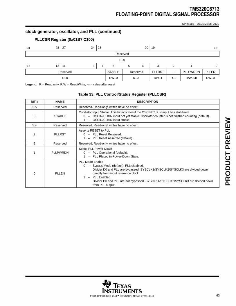
TMS320C6713FLOATING-POINT DIGITAL SIGNAL PROCESSOR
SPRS186 – DECEMBER 2001
63POST OFFICE BOX 1443 • HOUSTON, TEXAS 77251–1443
clock generator, oscillator, and PLL (continued)
PLLCSR Register (0x01B7 C100)
31 28 27 24 23 20 19 16
Reserved
R–0
15 12 11 8 7 6 5 4 3 2 1 0
Reserved STABLE Reserved PLLRST – PLLPWRDN PLLEN
R–0 RW–0 R–0 RW–1 R–0 R/W–0b RW–0
Legend: R = Read only, R/W = Read/Write; -n = value after reset
Table 33. PLL Control/Status Register (PLLCSR)
BIT # NAME DESCRIPTION
31:7 Reserved Reserved. Read-only, writes have no effect.
6 STABLEOscillator Input Stable. This bit indicates if the OSCIN/CLKIN input has stabilized.
0 – OSCIN/CLKIN input not yet stable. Oscillator counter is not finished counting (default).1 – OSCIN/CLKIN input stable.
5:4 Reserved Reserved. Read-only, writes have no effect.
3 PLLRSTAsserts RESET to PLL
0 – PLL Reset Released.1 – PLL Reset Asserted (default).
2 Reserved Reserved. Read-only, writes have no effect.
1 PLLPWRDNSelect PLL Power Down
0 – PLL Operational (default).1 – PLL Placed in Power-Down State.
0 PLLEN
PLL Mode Enable0 – Bypass Mode (default). PLL disabled.
Divider D0 and PLL are bypassed. SYSCLK1/SYSCLK2/SYSCLK3 are divided down directly from input reference clock.
1 – PLL Enabled.Divider D0 and PLL are not bypassed. SYSCLK1/SYSCLK2/SYSCLK3 are divided down from PLL output. P
RO
DU
CT
PR
EV
IEW

TMS320C6713FLOATING-POINT DIGITAL SIGNAL PROCESSOR
SPRS186 – DECEMBER 2001
64 POST OFFICE BOX 1443 • HOUSTON, TEXAS 77251–1443
clock generator, oscillator, and PLL (continued)
PLLM Register (0x01B7 C110)
31 28 27 24 23 20 19 16
Reserved
R–0
15 12 11 8 7 6 5 4 3 2 1 0
Reserved PLLM
R–0 R/W–0 0111
Legend: R = Read only, R/W = Read/Write; -n = value after reset
Table 34. PLL Multiplier Control Register (PLLM)
BIT # NAME DESCRIPTION
31:5 Reserved Reserved. Read-only, writes have no effect.
4:0 PLLM
PLL multiply mode [default is x8 (0 0111)].00000 = x1 01000 = x900001 = x2 01001 = x1000010 = x3 01010 = x1100011 = x4 01011 = x1200100 = x5 01100 = x1300101 = x6 01101 = x1400110 = x7 01110 = x1500111 = x8 01111 = x16
PLLM select values 10000 through 11111 are not supported.
PR
OD
UC
T P
RE
VIE
W
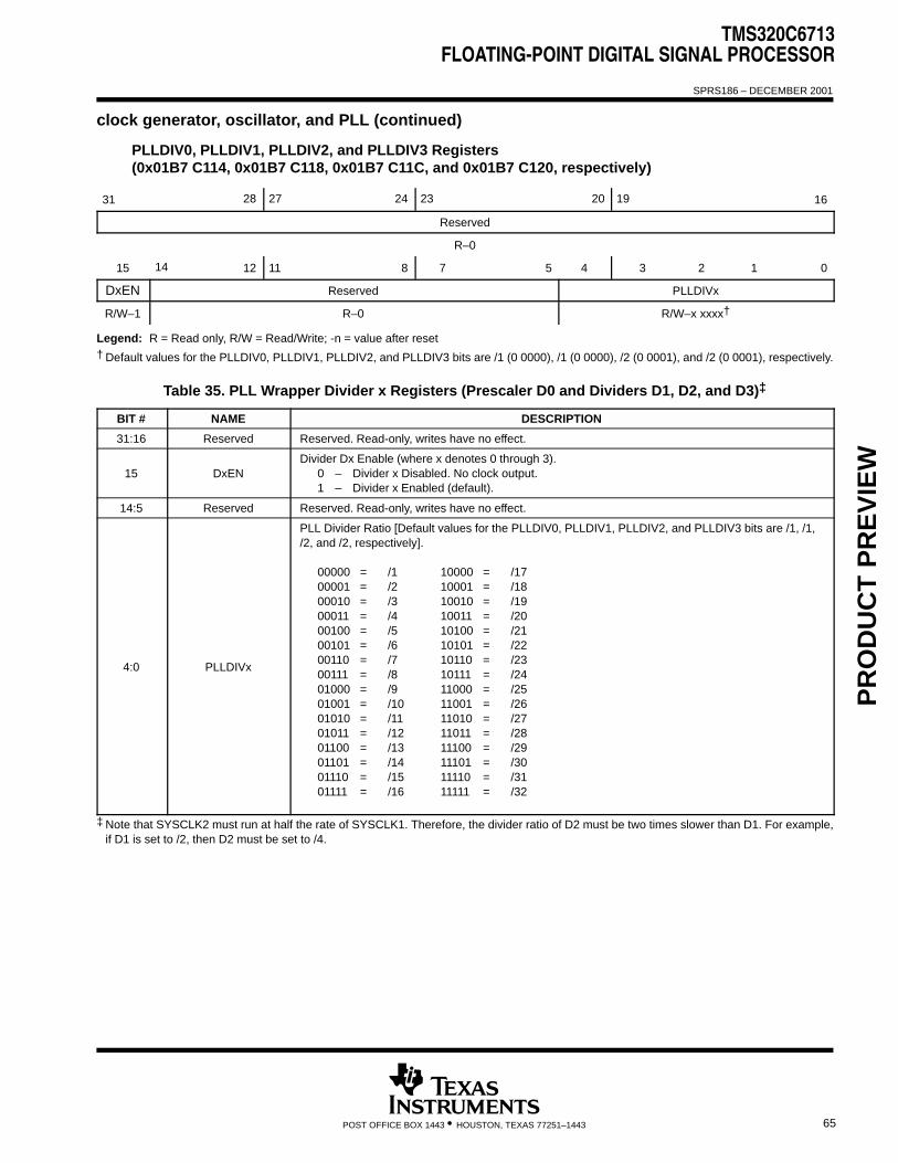
TMS320C6713FLOATING-POINT DIGITAL SIGNAL PROCESSOR
SPRS186 – DECEMBER 2001
65POST OFFICE BOX 1443 • HOUSTON, TEXAS 77251–1443
clock generator, oscillator, and PLL (continued)
PLLDIV0, PLLDIV1, PLLDIV2, and PLLDIV3 Registers (0x01B7 C114, 0x01B7 C118, 0x01B7 C11C, and 0x01B7 C120, respectively)
31 28 27 24 23 20 19 16
Reserved
R–0
15 14 12 11 8 7 5 4 3 2 1 0
DxEN Reserved PLLDIVx
R/W–1 R–0 R/W–x xxxx†
Legend: R = Read only, R/W = Read/Write; -n = value after reset† Default values for the PLLDIV0, PLLDIV1, PLLDIV2, and PLLDIV3 bits are /1 (0 0000), /1 (0 0000), /2 (0 0001), and /2 (0 0001), respectively.
Table 35. PLL Wrapper Divider x Registers (Prescaler D0 and Dividers D1, D2, and D3)‡
BIT # NAME DESCRIPTION
31:16 Reserved Reserved. Read-only, writes have no effect.
15 DxENDivider Dx Enable (where x denotes 0 through 3).
0 – Divider x Disabled. No clock output.1 – Divider x Enabled (default).
14:5 Reserved Reserved. Read-only, writes have no effect.
4:0 PLLDIVx
PLL Divider Ratio [Default values for the PLLDIV0, PLLDIV1, PLLDIV2, and PLLDIV3 bits are /1, /1,/2, and /2, respectively].
00000 = /1 10000 = /1700001 = /2 10001 = /1800010 = /3 10010 = /1900011 = /4 10011 = /2000100 = /5 10100 = /2100101 = /6 10101 = /2200110 = /7 10110 = /2300111 = /8 10111 = /2401000 = /9 11000 = /2501001 = /10 11001 = /2601010 = /11 11010 = /2701011 = /12 11011 = /2801100 = /13 11100 = /2901101 = /14 11101 = /3001110 = /15 11110 = /3101111 = /16 11111 = /32
‡ Note that SYSCLK2 must run at half the rate of SYSCLK1. Therefore, the divider ratio of D2 must be two times slower than D1. For example,if D1 is set to /2, then D2 must be set to /4.
PR
OD
UC
T P
RE
VIE
W

TMS320C6713FLOATING-POINT DIGITAL SIGNAL PROCESSOR
SPRS186 – DECEMBER 2001
66 POST OFFICE BOX 1443 • HOUSTON, TEXAS 77251–1443
clock generator, oscillator, and PLL (continued)
OSCDIV1 Register (0x01B7 C124)
31 28 27 24 23 20 19 16
Reserved
R–0
15 14 12 11 8 7 5 4 3 2 1 0
OD1EN Reserved OSCDIV1
R/W–1 R–0 R/W–0 0111
Legend: R = Read only, R/W = Read/Write; -n = value after reset
The OSCDIV1 register controls the oscillator divider 1 for CLKOUT3. The CLKOUT3 signal does not go throughthe PLL path.
Table 36. Oscillator Divider 1 Register (OSCDIV1)
BIT # NAME DESCRIPTION
31:16 Reserved Reserved. Read-only, writes have no effect.
15 OD1ENOscillator Divider 1 Enable.
0 – Oscillator Divider 1 Disabled.1 – Oscillator Divider 1 Enabled (default).
14:5 Reserved Reserved. Read-only, writes have no effect.
4:0 OSCDIV1
Oscillator Divider 1 Ratio [default is /8 (0 0111)].
00000 = /1 10000 = /1700001 = /2 10001 = /1800010 = /3 10010 = /1900011 = /4 10011 = /2000100 = /5 10100 = /2100101 = /6 10101 = /2200110 = /7 10110 = /2300111 = /8 10111 = /2401000 = /9 11000 = /2501001 = /10 11001 = /2601010 = /11 11010 = /2701011 = /12 11011 = /2801100 = /13 11100 = /2901101 = /14 11101 = /3001110 = /15 11110 = /3101111 = /16 11111 = /32
PR
OD
UC
T P
RE
VIE
W

TMS320C6713FLOATING-POINT DIGITAL SIGNAL PROCESSOR
SPRS186 – DECEMBER 2001
67POST OFFICE BOX 1443 • HOUSTON, TEXAS 77251–1443
absolute maximum ratings over operating case temperature range (unless otherwise noted)† Supply voltage range, CVDD (see Note 1) –0.3 V to 1.35 V. . . . . . . . . . . . . . . . . . . . . . . . . . . . . . . . . . . . . . . . . . . Supply voltage range, DVDD (see Note 1) –0.3 V to 4 V. . . . . . . . . . . . . . . . . . . . . . . . . . . . . . . . . . . . . . . . . . . . . Input voltage range –0.3 V to DVDD + 0.5 V. . . . . . . . . . . . . . . . . . . . . . . . . . . . . . . . . . . . . . . . . . . . . . . . . . . . . . . . Output voltage range –0.3 V to DVDD + 0.5 V. . . . . . . . . . . . . . . . . . . . . . . . . . . . . . . . . . . . . . . . . . . . . . . . . . . . . . Operating case temperature ranges, TC 0C to 90C. . . . . . . . . . . . . . . . . . . . . . . . . . . . . . . . . . . . . . . . . . . Storage temperature range, Tstg –65C to 150C. . . . . . . . . . . . . . . . . . . . . . . . . . . . . . . . . . . . . . . . . . . . . . .
† Stresses beyond those listed under “absolute maximum ratings” may cause permanent damage to the device. These are stress ratings only, andfunctional operation of the device at these or any other conditions beyond those indicated under “recommended operating conditions” is notimplied. Exposure to absolute-maximum-rated conditions for extended periods may affect device reliability.
NOTE 1: All voltage values are with respect to VSS.
recommended operating conditions‡
MIN NOM MAX UNIT
CVDD Supply voltage, Core referenced to VSS 1.14 1.2 1.26 V
DVDD Supply voltage, I/O referenced to VSS 3.13 3.3 3.47 V
V(C – D) Maximum supply voltage difference CVDD – DVDD 1.32 V
V(D – C) Maximum supply voltage difference DVDD – CVDD 2.75 V
VIH High-level input voltage 0.7*DVDD V
VIL Low-level input voltage 0.3*DVDD V
IOH High-level output current
All signals except TDO, EMU[5:0], ECLKOUT,CLKOUT2, CLKOUT3, SCL1, SDA1, SCL0,and SDA0
–8 mA
IOH High-level out ut currentTDO, EMU[5:0], ECLKOUT, CLKOUT2, andCLKOUT3
–16 mA
All signals except TDO, EMU[5:0], ECLKOUT,CLKOUT2, CLKOUT3, SCL1, SDA1, SCL0,and SDA0
8 mA
IOL Low-level output current TDO, EMU[5:0], ECLKOUT, CLKOUT2, andCLKOUT3
16 mA
SCL1, SDA1, SCL0, and SDA0 6 mA
TC Operating case temperature 0 90 C
‡ The core supply should be powered up at the same time as, or prior to (and powered down after), the I/O supply. Systems should be designedto ensure that neither supply is powered up for an extended period of time if the other supply is below the proper operating voltage.
PR
OD
UC
T P
RE
VIE
W
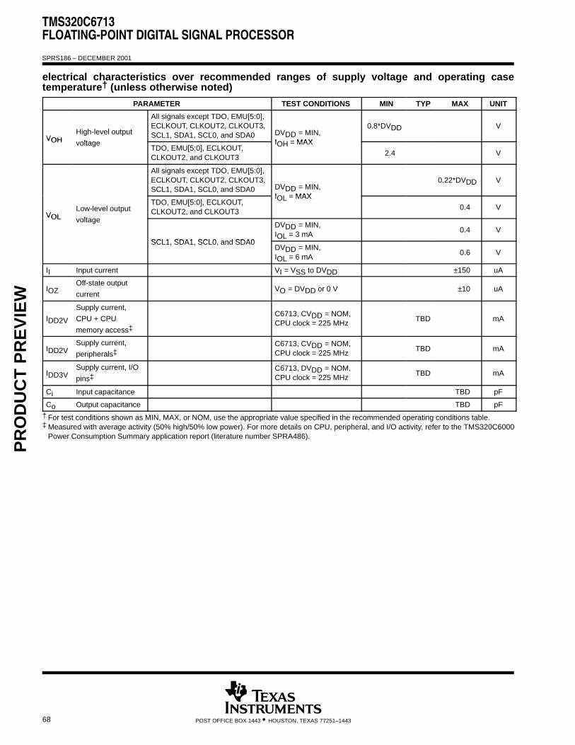
TMS320C6713FLOATING-POINT DIGITAL SIGNAL PROCESSOR
SPRS186 – DECEMBER 2001
68 POST OFFICE BOX 1443 • HOUSTON, TEXAS 77251–1443
electrical characteristics over recommended ranges of supply voltage and operating casetemperature† (unless otherwise noted)
PARAMETER TEST CONDITIONS MIN TYP MAX UNIT
VOHHigh-level output
lt
All signals except TDO, EMU[5:0],ECLKOUT, CLKOUT2, CLKOUT3,SCL1, SDA1, SCL0, and SDA0 DVDD = MIN,
IOH MAX
0.8*DVDD V
VOH voltageTDO, EMU[5:0], ECLKOUT,CLKOUT2, and CLKOUT3
IOH = MAX
2.4 V
All signals except TDO, EMU[5:0],ECLKOUT, CLKOUT2, CLKOUT3,SCL1, SDA1, SCL0, and SDA0 DVDD = MIN,
IOL MAX
0.22*DVDD V
VOLLow-level output
lt
TDO, EMU[5:0], ECLKOUT,CLKOUT2, and CLKOUT3
IOL = MAX
0.4 VVOL voltage
SCL1 SDA1 SCL0 and SDA0
DVDD = MIN,IOL = 3 mA
0.4 V
SCL1, SDA1, SCL0, and SDA0DVDD = MIN,IOL = 6 mA
0.6 V
II Input current VI = VSS to DVDD ±150 uA
IOZOff-state output
currentVO = DVDD or 0 V ±10 uA
IDD2V
Supply current,
CPU + CPU
memory access‡
C6713, CVDD = NOM, CPU clock = 225 MHz
TBD mA
IDD2VSupply current,
peripherals‡C6713, CVDD = NOM, CPU clock = 225 MHz
TBD mA
IDD3VSupply current, I/O
pins‡C6713, DVDD = NOM, CPU clock = 225 MHz
TBD mA
Ci Input capacitance TBD pF
Co Output capacitance TBD pF
† For test conditions shown as MIN, MAX, or NOM, use the appropriate value specified in the recommended operating conditions table.‡ Measured with average activity (50% high/50% low power). For more details on CPU, peripheral, and I/O activity, refer to the TMS320C6000
Power Consumption Summary application report (literature number SPRA486).
PR
OD
UC
T P
RE
VIE
W
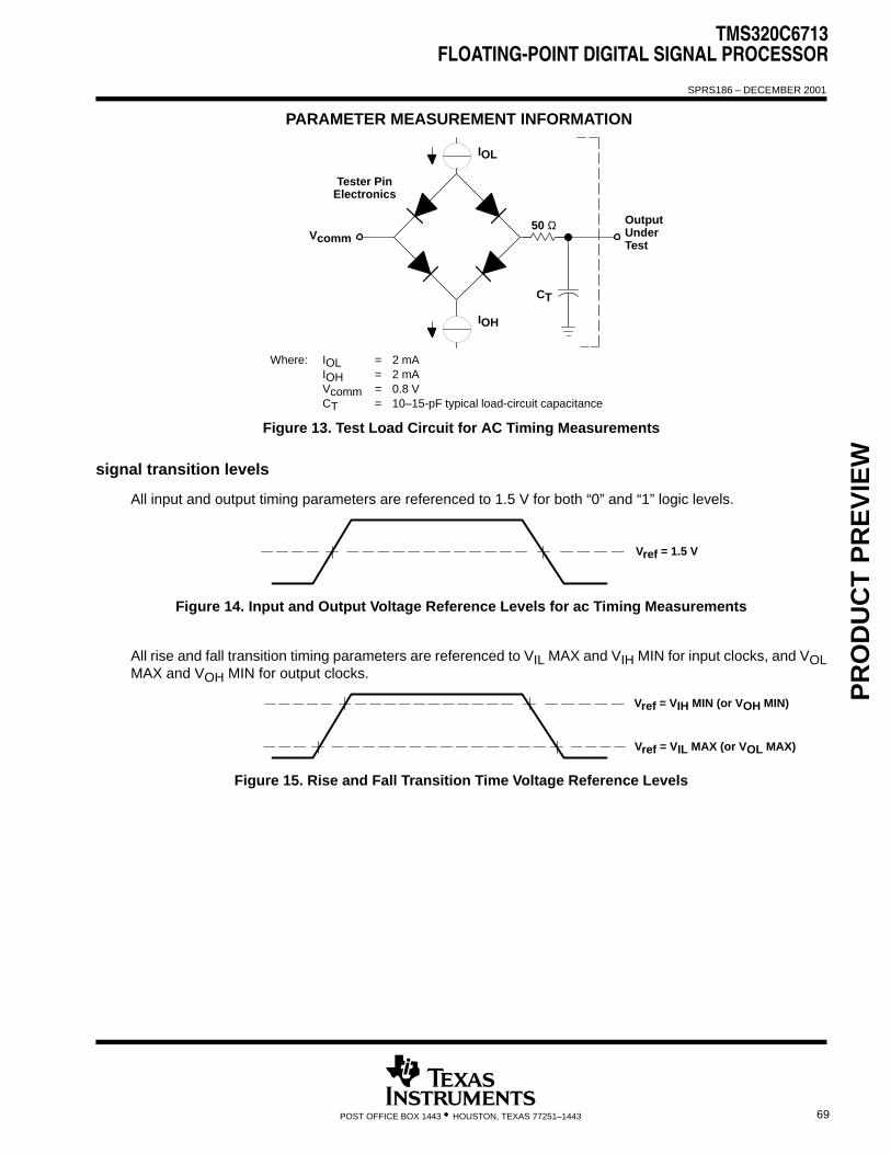
TMS320C6713FLOATING-POINT DIGITAL SIGNAL PROCESSOR
SPRS186 – DECEMBER 2001
69POST OFFICE BOX 1443 • HOUSTON, TEXAS 77251–1443
PARAMETER MEASUREMENT INFORMATION
Tester PinElectronics
Vcomm
IOL
CT
IOH
OutputUnderTest
50 Ω
Where: IOL = 2 mAIOH = 2 mAVcomm = 0.8 VCT = 10–15-pF typical load-circuit capacitance
Figure 13. Test Load Circuit for AC Timing Measurements
signal transition levels
All input and output timing parameters are referenced to 1.5 V for both “0” and “1” logic levels.
Vref = 1.5 V
Figure 14. Input and Output Voltage Reference Levels for ac Timing Measurements
All rise and fall transition timing parameters are referenced to VIL MAX and VIH MIN for input clocks, and VOLMAX and VOH MIN for output clocks.
Vref = VIL MAX (or VOL MAX)
Vref = VIH MIN (or VOH MIN)
Figure 15. Rise and Fall Transition Time Voltage Reference Levels
PR
OD
UC
T P
RE
VIE
W

TMS320C6713FLOATING-POINT DIGITAL SIGNAL PROCESSOR
SPRS186 – DECEMBER 2001
70 POST OFFICE BOX 1443 • HOUSTON, TEXAS 77251–1443
PARAMETER MEASUREMENT INFORMATION (CONTINUED)
timing parameters and board routing analysis
The timing parameter values specified in this data sheet do not include delays by board routings. As a goodboard design practice, such delays must always be taken into account. Timing values may be adjusted byincreasing/decreasing such delays. TI recommends utilizing the available I/O buffer information specification(IBIS) models to analyze the timing characteristics correctly. If needed, external logic hardware such as buffersmay be used to compensate any timing differences.
For inputs, timing is most impacted by the round-trip propagation delay from the DSP to the external device andfrom the external device to the DSP. This round-trip delay tends to negatively impact the input setup time margin,but also tends to improve the input hold time margins (see Table 37 and Figure 16).
Figure 16 represents a general transfer between the DSP and an external device. The figure also representsboard route delays and how they are perceived by the DSP and the external device.
PR
OD
UC
T P
RE
VIE
W
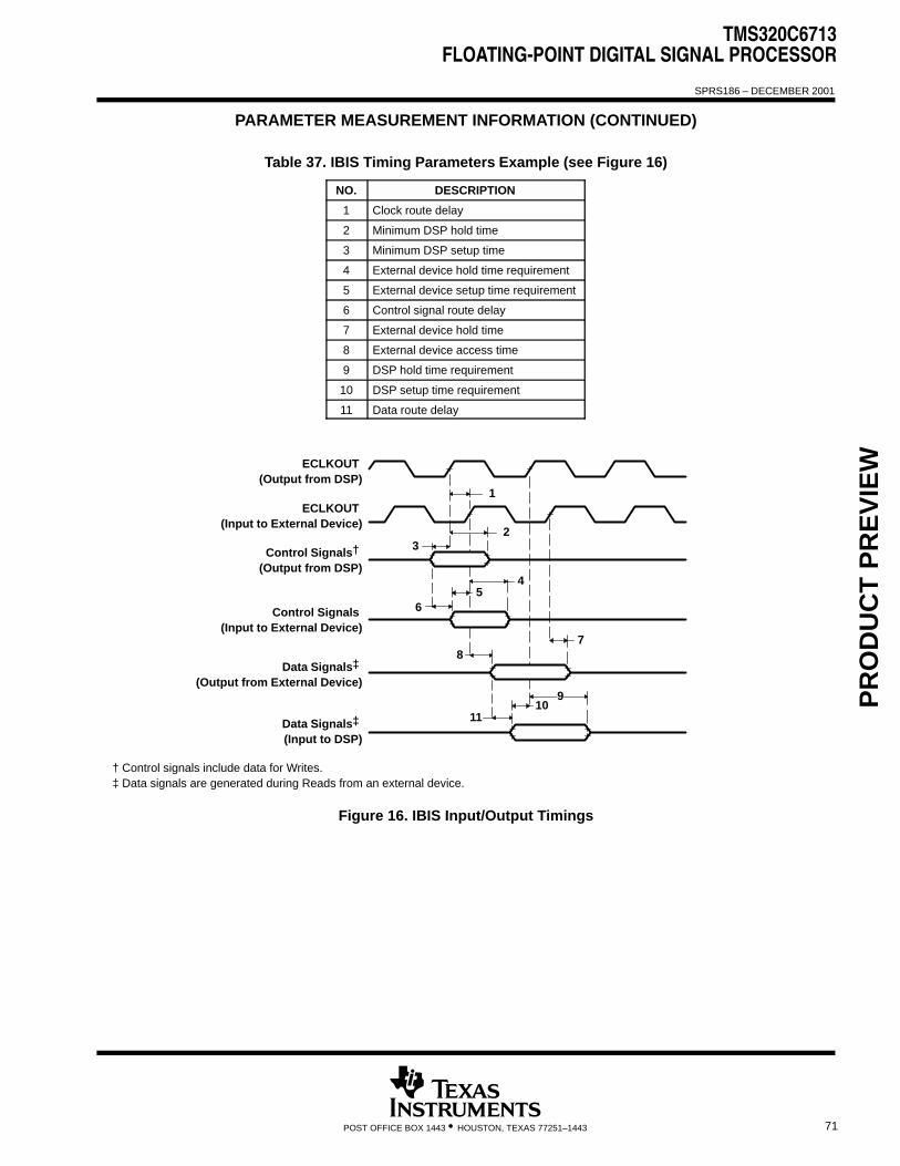
TMS320C6713FLOATING-POINT DIGITAL SIGNAL PROCESSOR
SPRS186 – DECEMBER 2001
71POST OFFICE BOX 1443 • HOUSTON, TEXAS 77251–1443
PARAMETER MEASUREMENT INFORMATION (CONTINUED)
Table 37. IBIS Timing Parameters Example (see Figure 16)
NO. DESCRIPTION
1 Clock route delay
2 Minimum DSP hold time
3 Minimum DSP setup time
4 External device hold time requirement
5 External device setup time requirement
6 Control signal route delay
7 External device hold time
8 External device access time
9 DSP hold time requirement
10 DSP setup time requirement
11 Data route delay
1
23
45
6
78
1011
ECLKOUT (Output from DSP)
ECLKOUT (Input to External Device)
Control Signals† (Output from DSP)
Control Signals (Input to External Device)
Data Signals‡ (Output from External Device)
Data Signals‡ (Input to DSP)
9
† Control signals include data for Writes.‡ Data signals are generated during Reads from an external device.
Figure 16. IBIS Input/Output Timings
PR
OD
UC
T P
RE
VIE
W
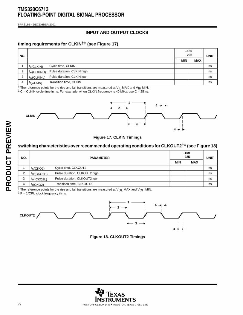
TMS320C6713FLOATING-POINT DIGITAL SIGNAL PROCESSOR
SPRS186 – DECEMBER 2001
72 POST OFFICE BOX 1443 • HOUSTON, TEXAS 77251–1443
INPUT AND OUTPUT CLOCKS
timing requirements for CLKIN†‡ (see Figure 17)
NO.
–150–225 UNITNO.
MIN MAXUNIT
1 tc(CLKIN) Cycle time, CLKIN ns
2 tw(CLKINH) Pulse duration, CLKIN high ns
3 tw(CLKINL) Pulse duration, CLKIN low ns
4 tt(CLKIN) Transition time, CLKIN ns
† The reference points for the rise and fall transitions are measured at VIL MAX and VIH MIN.‡ C = CLKIN cycle time in ns. For example, when CLKIN frequency is 40 MHz, use C = 25 ns.
CLKIN
1
2
3
4
4
Figure 17. CLKIN Timings
switching characteristics over recommended operating conditions for CLKOUT2†‡ (see Figure 18)
NO. PARAMETER
–150–225 UNITNO. PARAMETER
MIN MAXUNIT
1 tc(CKO2) Cycle time, CLKOUT2 ns
2 tw(CKO2H) Pulse duration, CLKOUT2 high ns
3 tw(CKO2L) Pulse duration, CLKOUT2 low ns
4 tt(CKO2) Transition time, CLKOUT2 ns
† The reference points for the rise and fall transitions are measured at VOL MAX and VOH MIN.‡ P = 1/CPU clock frequency in ns
CLKOUT2
1
2
3
4
4
Figure 18. CLKOUT2 Timings
PR
OD
UC
T P
RE
VIE
W

TMS320C6713FLOATING-POINT DIGITAL SIGNAL PROCESSOR
SPRS186 – DECEMBER 2001
73POST OFFICE BOX 1443 • HOUSTON, TEXAS 77251–1443
INPUT AND OUTPUT CLOCKS (CONTINUED)
switching characteristics over recommended operating conditions for CLKOUT3†‡(see Figure 19)
NO. PARAMETER
–150–225 UNITNO. PARAMETER
MIN MAXUNIT
1 tc(CKO3) Cycle time, CLKOUT3 ns
2 tw(CKO3H) Pulse duration, CLKOUT3 high ns
3 tw(CKO3L) Pulse duration, CLKOUT3 low ns
4 tt(CKO3) Transition time, CLKOUT3 ns
† The reference points for the rise and fall transitions are measured at VOL MAX and VOH MIN.‡ P = 1/CPU clock frequency in ns
CLKOUT3
1
2
3
4
4
Figure 19. CLKOUT3 Timings
timing requirements for ECLKIN† (see Figure 20)
NO.
–150–225 UNITNO.
MIN MAXUNIT
1 tc(EKI) Cycle time, ECLKIN ns
2 tw(EKIH) Pulse duration, ECLKIN high ns
3 tw(EKIL) Pulse duration, ECLKIN low ns
4 tt(EKI) Transition time, ECLKIN ns
† The reference points for the rise and fall transitions are measured at VIL MAX and VIH MIN.
ECLKIN
1
2
3
4
4
Figure 20. ECLKIN TimingsP
RO
DU
CT
PR
EV
IEW

TMS320C6713FLOATING-POINT DIGITAL SIGNAL PROCESSOR
SPRS186 – DECEMBER 2001
74 POST OFFICE BOX 1443 • HOUSTON, TEXAS 77251–1443
INPUT AND OUTPUT CLOCKS (CONTINUED)
switching characteristics over recommended operating conditions for ECLKOUTद
(see Figure 21)
NO. PARAMETER
–150–225 UNITNO. PARAMETER
MIN MAXUNIT
1 tc(EKO) Cycle time, ECLKOUT
2 tw(EKOH) Pulse duration, ECLKOUT high
3 tw(EKOL) Pulse duration, ECLKOUT low
4 tt(EKO) Transition time, ECLKOUT
5 td(EKIH-EKOH) Delay time, ECLKIN high to ECLKOUT high
6 td(EKIL-EKOL) Delay time, ECLKIN low to ECLKOUT low
‡ The reference points for the rise and fall transitions are measured at VOL MAX and VOH MIN.§ E = ECLKIN period in ns¶ EH is the high period of ECLKIN in ns and EL is the low period of ECLKIN in ns.
56 1
2 3
ECLKINECLKIN
ECLKOUT
4 4
Figure 21. ECLKOUT Timings
PR
OD
UC
T P
RE
VIE
W

TMS320C6713FLOATING-POINT DIGITAL SIGNAL PROCESSOR
SPRS186 – DECEMBER 2001
75POST OFFICE BOX 1443 • HOUSTON, TEXAS 77251–1443
ASYNCHRONOUS MEMORY TIMING
timing requirements for asynchronous memory cycles†‡§ (see Figure 22–Figure 23)
NO.
–150–225 UNITNO.
MIN MAXUNIT
3 tsu(EDV-AREH) Setup time, EDx valid before ARE high
4 th(AREH-EDV) Hold time, EDx valid after ARE high
6 tsu(ARDY-EKOH)Setup time, ARDY valid before ECLKOUT high
7 th(EKOH-ARDY)Hold time, ARDY valid after ECLKOUT high
† To ensure data setup time, simply program the strobe width wide enough. ARDY is internally synchronized. The ARDY signal is recognized inthe cycle for which the setup and hold time is met. To use ARDY as an asynchronous input, the pulse width of the ARDY signal should be wideenough (e.g., pulse width = 2E) to ensure setup and hold time is met.
‡ RS = Read setup, RST = Read strobe, RH = Read hold, WS = Write setup, WST = Write strobe, WH = Write hold. These parameters areprogrammed via the EMIF CE space control registers.
§ E = ECLKOUT period in ns
switching characteristics over recommended operating conditions for asynchronous memorycycles‡§¶ (see Figure 22–Figure 23)
NO. PARAMETER
–150–225 UNITNO. PARAMETERMIN MAX
UNIT
1 tosu(SELV-AREL) Output setup time, select signals valid to ARE low
2 toh(AREH-SELIV)Output hold time, ARE high to select signalsinvalid
5 td(EKOH-AREV) Delay time, ECLKOUT high to ARE vaild
8 tosu(SELV-AWEL) Output setup time, select signals valid to AWE low
9 toh(AWEH-SELIV) Output hold time, AWE high to select signals invalid
10 td(EKOH-AWEV) Delay time, ECLKOUT high to AWE vaild
‡ RS = Read setup, RST = Read strobe, RH = Read hold, WS = Write setup, WST = Write strobe, WH = Write hold. These parameters areprogrammed via the EMIF CE space control registers.
§ E = ECLKOUT period in ns¶ Select signals include: CEx, BE[3:0], EA[21:2], AOE; and for writes, include ED[31:0].
PR
OD
UC
T P
RE
VIE
W
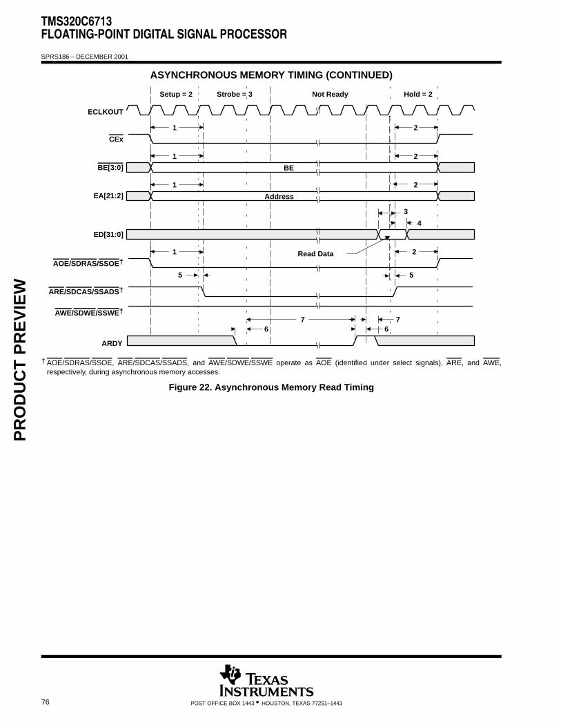
TMS320C6713FLOATING-POINT DIGITAL SIGNAL PROCESSOR
SPRS186 – DECEMBER 2001
76 POST OFFICE BOX 1443 • HOUSTON, TEXAS 77251–1443
ASYNCHRONOUS MEMORY TIMING (CONTINUED)
Setup = 2 Strobe = 3 Not Ready Hold = 2
BE
Address
Read Data 21
21
21
21
5
4
3
ARDY
7 766
5
ECLKOUT
CEx
EA[21:2]
ED[31:0]
AOE/SDRAS/SSOE†
ARE/SDCAS/SSADS†
BE[3:0]
AWE/SDWE/SSWE†
† AOE/SDRAS/SSOE, ARE/SDCAS/SSADS, and AWE/SDWE/SSWE operate as AOE (identified under select signals), ARE, and AWE,respectively, during asynchronous memory accesses.
Figure 22. Asynchronous Memory Read Timing
PR
OD
UC
T P
RE
VIE
W

TMS320C6713FLOATING-POINT DIGITAL SIGNAL PROCESSOR
SPRS186 – DECEMBER 2001
77POST OFFICE BOX 1443 • HOUSTON, TEXAS 77251–1443
ASYNCHRONOUS MEMORY TIMING (CONTINUED)
Setup = 2 Strobe = 3 Not Ready Hold = 2
BE
Address
Write Data
1010
98
98
98
98
7766
ECLKOUT
CEx
EA[21:2]
ED[31:0]
BE[3:0]
ARDY
AOE/SDRAS/SSOE†
ARE/SDCAS/SSADS†
AWE/SDWE/SSWE†
† AOE/SDRAS/SSOE, ARE/SDCAS/SSADS, and AWE/SDWE/SSWE operate as AOE (identified under select signals), ARE, and AWE,respectively, during asynchronous memory accesses.
Figure 23. Asynchronous Memory Write Timing
PR
OD
UC
T P
RE
VIE
W

TMS320C6713FLOATING-POINT DIGITAL SIGNAL PROCESSOR
SPRS186 – DECEMBER 2001
78 POST OFFICE BOX 1443 • HOUSTON, TEXAS 77251–1443
SYNCHRONOUS-BURST MEMORY TIMING
timing requirements for synchronous-burst SRAM cycles† (see Figure 24)
NO.
–150–225 UNITNO.
MIN MAXUNIT
6 tsu(EDV-EKOH) Setup time, read EDx valid before ECLKOUT high
7 th(EKOH-EDV) Hold time, read EDx valid after ECLKOUT high
† The C6713 SBSRAM interface takes advantage of the internal burst counter in the SBSRAM. Accesses default to incrementing 4-word bursts,but random bursts and decrementing bursts are done by interrupting bursts in progress. All burst types can sustain continuous data flow.
switching characteristics over recommended operating conditions for synchronous-burst SRAMcycles†‡ (see Figure 24 and Figure 25)
NO. PARAMETER
–150–225 UNITNO. PARAMETER
MIN MAXUNIT
1 td(EKOH-CEV) Delay time, ECLKOUT high to CEx valid
2 td(EKOH-BEV) Delay time, ECLKOUT high to BEx valid
3 td(EKOH-BEIV) Delay time, ECLKOUT high to BEx invalid
4 td(EKOH-EAV) Delay time, ECLKOUT high to EAx valid
5 td(EKOH-EAIV) Delay time, ECLKOUT high to EAx invalid
8 td(EKOH-ADSV) Delay time, ECLKOUT high to ARE/SDCAS/SSADS valid
9 td(EKOH-OEV) Delay time, ECLKOUT high to, AOE/SDRAS/SSOE valid
10 td(EKOH-EDV) Delay time, ECLKOUT high to EDx valid
11 td(EKOH-EDIV) Delay time, ECLKOUT high to EDx invalid
12 td(EKOH-WEV) Delay time, ECLKOUT high to AWE/SDWE/SSWE valid
† The C6713 SBSRAM interface takes advantage of the internal burst counter in the SBSRAM. Accesses default to incrementing 4-word bursts,but random bursts and decrementing bursts are done by interrupting bursts in progress. All burst types can sustain continuous data flow.
‡ ARE/SDCAS/SSADS, AOE/SDRAS/SSOE, and AWE/SDWE/SSWE operate as SSADS, SSOE, and SSWE, respectively, during SBSRAMaccesses.
PR
OD
UC
T P
RE
VIE
W

TMS320C6713FLOATING-POINT DIGITAL SIGNAL PROCESSOR
SPRS186 – DECEMBER 2001
79POST OFFICE BOX 1443 • HOUSTON, TEXAS 77251–1443
SYNCHRONOUS-BURST MEMORY TIMING (CONTINUED)
ECLKOUT
CEx
BE[3:0]
EA[21:2]
ED[31:0]
ARE/SDCAS/SSADS†
AOE/SDRAS/SSOE†
AWE/SDWE/SSWE†
BE1 BE2 BE3 BE4
EA
Q1 Q2 Q3 Q4
9
1
4 5
8 8
9
67
3
1
2
† ARE/SDCAS/SSADS, AOE/SDRAS/SSOE, and AWE/SDWE/SSWE operate as SSADS, SSOE, and SSWE, respectively, during SBSRAMaccesses.
Figure 24. SBSRAM Read Timing
ECLKOUT
CEx
BE[3:0]
EA[21:2]
ED[31:0]
ARE/SDCAS/SSADS†
AOE/SDRAS/SSOE†
AWE/SDWE/SSWE†
BE1 BE2 BE3 BE4
Q1 Q2 Q3 Q4
12
11
3
1
8
12
10
4
2
1
8
5
EA
† ARE/SDCAS/SSADS, AOE/SDRAS/SSOE, and AWE/SDWE/SSWE operate as SSADS, SSOE, and SSWE, respectively, during SBSRAMaccesses.
Figure 25. SBSRAM Write Timing
PR
OD
UC
T P
RE
VIE
W
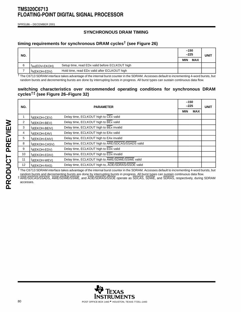
TMS320C6713FLOATING-POINT DIGITAL SIGNAL PROCESSOR
SPRS186 – DECEMBER 2001
80 POST OFFICE BOX 1443 • HOUSTON, TEXAS 77251–1443
SYNCHRONOUS DRAM TIMING
timing requirements for synchronous DRAM cycles† (see Figure 26)
NO.
–150–225 UNITNO.
MIN MAXUNIT
6 tsu(EDV-EKOH) Setup time, read EDx valid before ECLKOUT high
7 th(EKOH-EDV) Hold time, read EDx valid after ECLKOUT high
† The C6713 SDRAM interface takes advantage of the internal burst counter in the SDRAM. Accesses default to incrementing 4-word bursts, butrandom bursts and decrementing bursts are done by interrupting bursts in progress. All burst types can sustain continuous data flow.
switching characteristics over recommended operating conditions for synchronous DRAMcycles†‡ (see Figure 26–Figure 32)
NO. PARAMETER
–150–225 UNITNO. PARAMETER
MIN MAXUNIT
1 td(EKOH-CEV) Delay time, ECLKOUT high to CEx valid
2 td(EKOH-BEV) Delay time, ECLKOUT high to BEx valid
3 td(EKOH-BEIV) Delay time, ECLKOUT high to BEx invalid
4 td(EKOH-EAV) Delay time, ECLKOUT high to EAx valid
5 td(EKOH-EAIV) Delay time, ECLKOUT high to EAx invalid
8 td(EKOH-CASV) Delay time, ECLKOUT high to ARE/SDCAS/SSADS valid
9 td(EKOH-EDV) Delay time, ECLKOUT high to EDx valid
10 td(EKOH-EDIV) Delay time, ECLKOUT high to EDx invalid
11 td(EKOH-WEV) Delay time, ECLKOUT high to AWE/SDWE/SSWE valid
12 td(EKOH-RAS) Delay time, ECLKOUT high to, AOE/SDRAS/SSOE valid
† The C6713 SDRAM interface takes advantage of the internal burst counter in the SDRAM. Accesses default to incrementing 4-word bursts, butrandom bursts and decrementing bursts are done by interrupting bursts in progress. All burst types can sustain continuous data flow.
‡ ARE/SDCAS/SSADS, AWE/SDWE/SSWE, and AOE/SDRAS/SSOE operate as SDCAS, SDWE, and SDRAS, respectively, during SDRAMaccesses.
PR
OD
UC
T P
RE
VIE
W

TMS320C6713FLOATING-POINT DIGITAL SIGNAL PROCESSOR
SPRS186 – DECEMBER 2001
81POST OFFICE BOX 1443 • HOUSTON, TEXAS 77251–1443
SYNCHRONOUS DRAM TIMING (CONTINUED)
ECLKOUT
CEx
BE[3:0]
EA[11:2]
ED[31:0]
EA12
AOE/SDRAS/SSOE†
ARE/SDCAS/SSADS†
AWE/SDWE/SSWE†
EA[21:13]
BE1 BE2 BE3 BE4
Bank
Column
D1 D2 D3 D4
8
76
5
5
5
1
32
8
4
4
4
1
READ
† ARE/SDCAS/SSADS, AWE/SDWE/SSWE, and AOE/SDRAS/SSOE operate as SDCAS, SDWE, and SDRAS, respectively, during SDRAMaccesses.
Figure 26. SDRAM Read Command (CAS Latency 3)
PR
OD
UC
T P
RE
VIE
W

TMS320C6713FLOATING-POINT DIGITAL SIGNAL PROCESSOR
SPRS186 – DECEMBER 2001
82 POST OFFICE BOX 1443 • HOUSTON, TEXAS 77251–1443
SYNCHRONOUS DRAM TIMING (CONTINUED)
ECLKOUT
CEx
BE[3:0]
EA[11:2]
ED[31:0]
AOE/SDRAS/SSOE†
ARE/SDCAS/SSADS†
AWE/SDWE/SSWE†
EA12
EA[21:13]
BE1 BE2 BE3 BE4
Bank
Column
D1 D2 D3 D4
11
8
9
5
5
5
4
2
11
8
9
4
4
2
1
10
3
4
WRITE
† ARE/SDCAS/SSADS, AWE/SDWE/SSWE, and AOE/SDRAS/SSOE operate as SDCAS, SDWE, and SDRAS, respectively, during SDRAMaccesses.
Figure 27. SDRAM Write Command
PR
OD
UC
T P
RE
VIE
W

TMS320C6713FLOATING-POINT DIGITAL SIGNAL PROCESSOR
SPRS186 – DECEMBER 2001
83POST OFFICE BOX 1443 • HOUSTON, TEXAS 77251–1443
SYNCHRONOUS DRAM TIMING (CONTINUED)
ECLKOUT
CEx
BE[3:0]
EA[21:13]
ED[31:0]
EA12
AOE/SDRAS/SSOE†
ARE/SDCAS/SSADS†
AWE/SDWE/SSWE†
Bank Activate
Row Address
Row Address
12
5
5
5
1
EA[11:2]
ACTV
12
4
4
4
1
† ARE/SDCAS/SSADS, AWE/SDWE/SSWE, and AOE/SDRAS/SSOE operate as SDCAS, SDWE, and SDRAS, respectively, during SDRAMaccesses.
Figure 28. SDRAM ACTV Command
ECLKOUT
CEx
BE[3:0]
EA[21:13, 11:2]
ED[31:0]
EA12
AOE/SDRAS/SSOE†
ARE/SDCAS/SSADS†
AWE/SDWE/SSWE†11
12
5
1
DCAB
11
12
4
1
† ARE/SDCAS/SSADS, AWE/SDWE/SSWE, and AOE/SDRAS/SSOE operate as SDCAS, SDWE, and SDRAS, respectively, during SDRAMaccesses.
Figure 29. SDRAM DCAB Command
PR
OD
UC
T P
RE
VIE
W

TMS320C6713FLOATING-POINT DIGITAL SIGNAL PROCESSOR
SPRS186 – DECEMBER 2001
84 POST OFFICE BOX 1443 • HOUSTON, TEXAS 77251–1443
SYNCHRONOUS DRAM TIMING (CONTINUED)
ECLKOUT
CEx
BE[3:0]
EA[21:13]
ED[31:0]
EA12
AOE/SDRAS/SSOE†
ARE/SDCAS/SSADS†
AWE/SDWE/SSWE†
EA[11:2]
Bank
11
12
5
5
1
DEAC
11
12
4
4
1
† ARE/SDCAS/SSADS, AWE/SDWE/SSWE, and AOE/SDRAS/SSOE operate as SDCAS, SDWE, and SDRAS, respectively, during SDRAMaccesses.
Figure 30. SDRAM DEAC Command
ECLKOUT
CEx
BE[3:0]
EA[21:2]
ED[31:0]
EA12
AOE/SDRAS/SSOE†
ARE/SDCAS/SSADS†
AWE/SDWE/SSWE†
8
12
1
REFR
8
12
1
† ARE/SDCAS/SSADS, AWE/SDWE/SSWE, and AOE/SDRAS/SSOE operate as SDCAS, SDWE, and SDRAS, respectively, during SDRAMaccesses.
Figure 31. SDRAM REFR Command
PR
OD
UC
T P
RE
VIE
W

TMS320C6713FLOATING-POINT DIGITAL SIGNAL PROCESSOR
SPRS186 – DECEMBER 2001
85POST OFFICE BOX 1443 • HOUSTON, TEXAS 77251–1443
SYNCHRONOUS DRAM TIMING (CONTINUED)
ECLKOUT
CEx
BE[3:0]
EA[21:2]
ED[31:0]
AOE/SDRAS/SSOE†
ARE/SDCAS/SSADS†
AWE/SDWE/SSWE†
MRS value
11
8
12
5
1
MRS
11
8
12
4
1
† ARE/SDCAS/SSADS, AWE/SDWE/SSWE, and AOE/SDRAS/SSOE operate as SDCAS, SDWE, and SDRAS, respectively, during SDRAMaccesses.
Figure 32. SDRAM MRS Command
PR
OD
UC
T P
RE
VIE
W

TMS320C6713FLOATING-POINT DIGITAL SIGNAL PROCESSOR
SPRS186 – DECEMBER 2001
86 POST OFFICE BOX 1443 • HOUSTON, TEXAS 77251–1443
HOLD/HOLDA TIMING
timing requirements for the HOLD/HOLDA cycles† (see Figure 33)
NO.
–150–225 UNITNO.
MIN MAXUNIT
3 toh(HOLDAL-HOLDL) Output hold time, HOLD low after HOLDA low
† E = ECLKIN period in ns
switching characteristics over recommended operating conditions for the HOLD/HOLDA cycles†‡(see Figure 33)
NO. PARAMETER
–150–225 UNITNO. PARAMETER
MIN MAXUNIT
1 td(HOLDL-EMHZ) Delay time, HOLD low to EMIF Bus high impedance
2 td(EMHZ-HOLDAL) Delay time, EMIF Bus high impedance to HOLDA low
4 td(HOLDH-EMLZ) Delay time, HOLD high to EMIF Bus low impedance
5 td(EMLZ-HOLDAH) Delay time, EMIF Bus low impedance to HOLDA high
† E = ECLKIN period in ns‡ EMIF Bus consists of CE[3:0], BE[3:0], ED[31:0], EA[21:2], ARE/SDCAS/SSADS, AOE/SDRAS/SSOE, and AWE/SDWE/SSWE.§ All pending EMIF transactions are allowed to complete before HOLDA is asserted. If no bus transactions are occurring, then the minimum delay
time can be achieved. Also, bus hold can be indefinitely delayed by setting NOHOLD = 1.
HOLD
HOLDA
EMIF Bus†
DSP Owns BusExternal Requestor
Owns Bus DSP Owns Bus
C6713 C67131
3
2 5
4
† EMIF Bus consists of CE[3:0], BE[3:0], ED[31:0], EA[21:2], ARE/SDCAS/SSADS, AOE/SDRAS/SSOE, and AWE/SDWE/SSWE.
Figure 33. HOLD/HOLDA Timing
PR
OD
UC
T P
RE
VIE
W
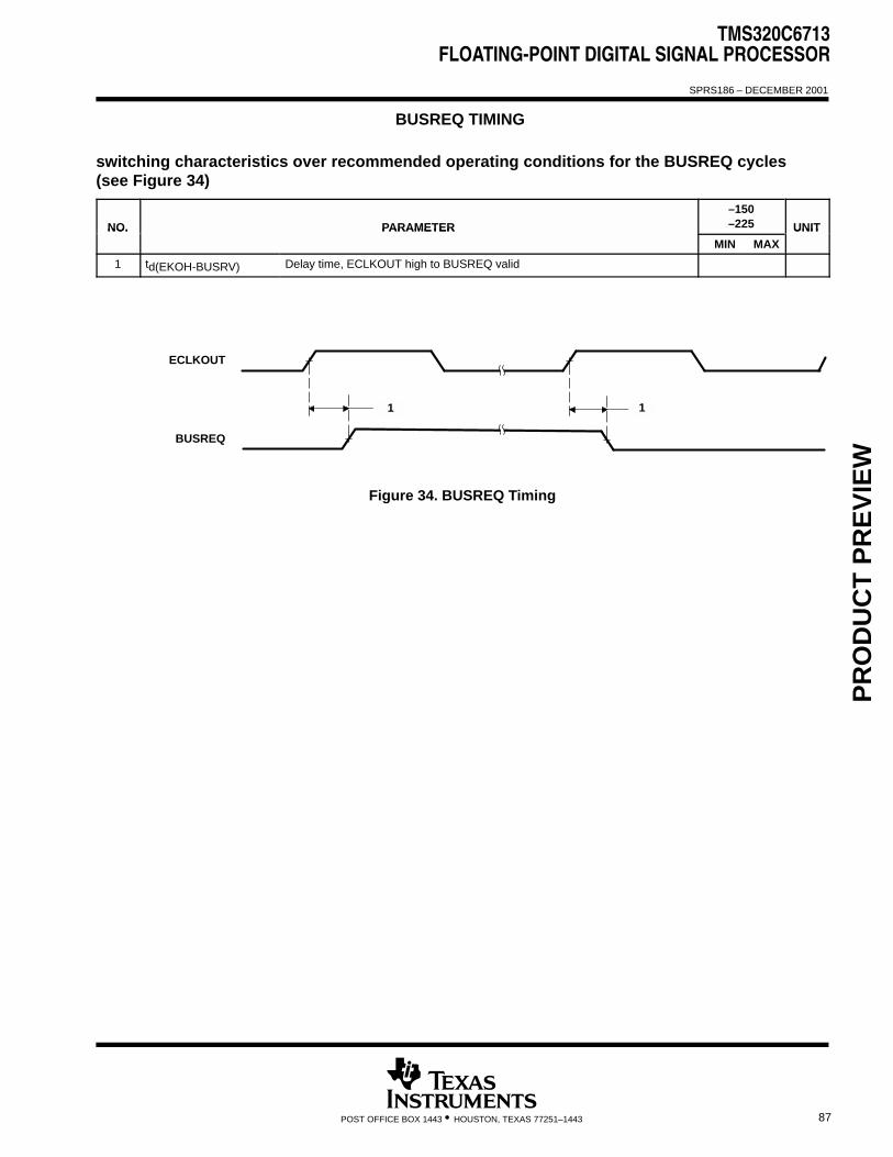
TMS320C6713FLOATING-POINT DIGITAL SIGNAL PROCESSOR
SPRS186 – DECEMBER 2001
87POST OFFICE BOX 1443 • HOUSTON, TEXAS 77251–1443
BUSREQ TIMING
switching characteristics over recommended operating conditions for the BUSREQ cycles(see Figure 34)
NO. PARAMETER
–150–225 UNITNO. PARAMETER
MIN MAXUNIT
1 td(EKOH-BUSRV) Delay time, ECLKOUT high to BUSREQ valid
ECLKOUT
1
BUSREQ
1
Figure 34. BUSREQ Timing
PR
OD
UC
T P
RE
VIE
W

TMS320C6713FLOATING-POINT DIGITAL SIGNAL PROCESSOR
SPRS186 – DECEMBER 2001
88 POST OFFICE BOX 1443 • HOUSTON, TEXAS 77251–1443
RESET TIMING
timing requirements for reset† (see Figure 35)
NO.
–150–225 UNITNO.
MIN MAXUNIT
1 tWidth of the RESET pulse (PLL stable)‡
1 tw(RST) Width of the RESET pulse (PLL needs to sync up)§
14 tsu(HD) Setup time, HD boot configuration bits valid before RESET high¶
15 th(HD) Hold time, HD boot configuration bits valid after RESET high¶
† P = 1/CPU clock frequency in ns. For example, when running parts at 225 MHz, use P = 4.4 ns.‡ This parameter applies to CLKMODE x1 when CLKIN is stable, and applies to CLKMODE x4 when CLKIN and PLL are stable.§ This parameter applies to CLKMODE x4 only (it does not apply to CLKMODE x1). The RESET signal is not connected internally to the clock PLL
circuit. The PLL, however, may need up to 250 µs to stabilize following device power up or after PLL configuration has been changed. Duringthat time, RESET must be asserted to ensure proper device operation. See the clock generator, oscillator, and PLL section for PLL lock times.
¶ Boot and device configurations consist of: HD[15:12, 8, 4:3].
switching characteristics over recommended operating conditions during reset†#|| (see Figure 35)
NO. PARAMETER
–150–225 UNITNO. PARAMETER
MIN MAXUNIT
2 td(RSTL-ECKI) Delay time, RESET low to ECLKIN synchronized internally
3 td(RSTH-ECKI) Delay time, RESET high to ECLKIN synchronized internally
4 td(RSTL-EMIFZHZ) Delay time, RESET low to EMIF Z group high impedance
5 td(RSTH-EMIFZV) Delay time, RESET high to EMIF Z group valid
6 td(RSTL-EMIFHIV) Delay time, RESET low to EMIF high group invalid
7 td(RSTH-EMIFHV) Delay time, RESET high to EMIF high group valid
8 td(RSTL-EMIFLIV) Delay time, RESET low to EMIF low group invalid
9 td(RSTH-EMIFLV) Delay time, RESET high to EMIF low group valid
10 td(RSTL-HIGHIV) Delay time, RESET low to high group invalid
11 td(RSTH-HIGHV) Delay time, RESET high to high group valid
12 td(RSTL-ZHZ) Delay time, RESET low to Z group high impedance
13 td(RSTH-ZV) Delay time, RESET high to Z group valid
† P = 1/CPU clock frequency in ns. For example, when running parts at 225 MHz, use P = 4.4 ns.# E = ECLKIN period in ns|| EMIF Z group consists of: EA[21:2], ED[31:0], CE[3:0], BE[3:0], ARE/SDCAS/SSADS, AWE/SDWE/SSWE, and AOE/SDRAS/SSOE
EMIF high group consists of: HOLDAEMIF low group consists of: BUSREQHigh group consists of: HRDY/ACLKR1 and HINT/GP[1]Z group consists of: HD[11:9, 7:5, 2:0], CLKX0, CLKX1, FSX0, FSX1, DX0, DX1, CLKR0, CLKR1, FSR0, FSR1, TOUT0, and TOUT1.
PR
OD
UC
T P
RE
VIE
W

TMS320C6713FLOATING-POINT DIGITAL SIGNAL PROCESSOR
SPRS186 – DECEMBER 2001
89POST OFFICE BOX 1443 • HOUSTON, TEXAS 77251–1443
RESET TIMING (CONTINUED)
1312
1110
98
76
54
32
15
14
1
CLKOUT2
RESET
ECLKIN
EMIF Z Group†
EMIF High Group†
EMIF Low Group†
High Group†
Z Group†
Boot and Device Configurations‡
† EMIF Z group consists of: EA[21:2], ED[31:0], CE[3:0], BE[3:0], ARE/SDCAS/SSADS, AWE/SDWE/SSWE, and AOE/SDRAS/SSOEEMIF high group consists of: HOLDAEMIF low group consists of: BUSREQHigh group consists of: HRDY/ACLKR1 and HINT/GP[1]Z group consists of: HD[11:9, 7:5, 2:0], CLKX0/ACLKX0, CLKX1/AMUTE0, FSX0/AFSX0, FSX1, DX0/AXR0[1], DX1/AXR0[5],
CLKR0/ACLKR0, CLKR1/AXR0[6], FSR0/AFSR0, FSR1/AXR0[7], TOUT0/AXR0[2], and TOUT1/AXR0[4].‡ Boot and device configurations consist of: HD[15:12, 8, 4:3].
Figure 35. Reset Timing
PR
OD
UC
T P
RE
VIE
W
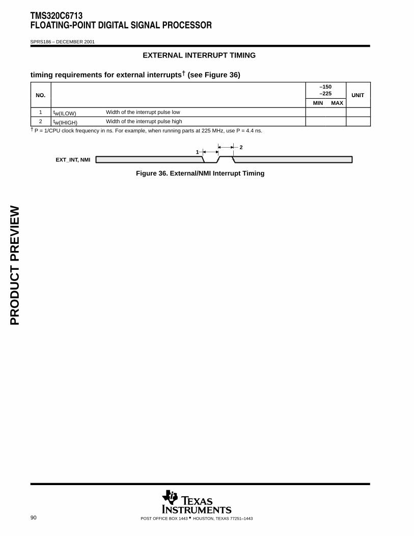
TMS320C6713FLOATING-POINT DIGITAL SIGNAL PROCESSOR
SPRS186 – DECEMBER 2001
90 POST OFFICE BOX 1443 • HOUSTON, TEXAS 77251–1443
EXTERNAL INTERRUPT TIMING
timing requirements for external interrupts† (see Figure 36)
NO.
–150–225 UNITNO.
MIN MAXUNIT
1 tw(ILOW) Width of the interrupt pulse low
2 tw(IHIGH) Width of the interrupt pulse high
† P = 1/CPU clock frequency in ns. For example, when running parts at 225 MHz, use P = 4.4 ns.
21
EXT_INT, NMI
Figure 36. External/NMI Interrupt Timing
PR
OD
UC
T P
RE
VIE
W

TMS320C6713FLOATING-POINT DIGITAL SIGNAL PROCESSOR
SPRS186 – DECEMBER 2001
91POST OFFICE BOX 1443 • HOUSTON, TEXAS 77251–1443
MULTICHANNEL AUDIO SERIAL PORT (McASP) TIMING
timing requirements for McASP†‡ (see Figure 37 and Figure 38)
NO.
–150–225 UNITNO.
MIN MAXUNIT
1 tc(AHCKRX) Cycle time, AHCLKR/X
2 tw(AHCKRX) Pulse duration, AHCLKR/X high or low
3 t Cycle time ACLKR/XACLKR/X int
3 tc(CKRX) Cycle time, ACLKR/XACLKR/X ext
4 t Pulse duration ACLKR/X high or lowACLKR/X int
4 tw(CKRX) Pulse duration, ACLKR/X high or lowACLKR/X ext
5 t Setup time AFSR/X input valid before ACLKR/X latches dataACLKR/X int
5 tsu(FRXC-KRX) Setup time, AFSR/X input valid before ACLKR/X latches dataACLKR/X ext
6 t Hold time AFSR/X input valid after ACLKR/X latches dataACLKR/X int
6 th(CKRX-FRX) Hold time, AFSR/X input valid after ACLKR/X latches dataACLKR/X ext
7 t Setup time AXR input valid before ACLKR/X latches dataACLKR/X int
7 tsu(AXR-CKRX) Setup time, AXR input valid before ACLKR/X latches dataACLKR/X ext
8 t Hold time AXR input valid after ACLKR/X latches dataACLKR/X int
8 th(CKRX-AXR) Hold time, AXR input valid after ACLKR/X latches dataACLKR/X ext
switching characteristics over recommended operating conditions for McASP (see Figure 37 and Figure 38)
NO. PARAMETER
–150–225 UNITNO. PARAMETER
MIN MAXUNIT
9 tc(AHCKRX) Cycle time, AHCLKR/X
10 tw(AHCKRX) Pulse duration, AHCLKR/X high or low
11 t Cycle time ACLKR/XACLKR/X int
11 tc(CKRX) Cycle time, ACLKR/XACLKR/X ext
12 t Pulse duration ACLKR/X high or lowACLKR/X int
12 tw(CKRX) Pulse duration, ACLKR/X high or lowACLKR/X ext
13 t Delay time ACLKR/X transmit edge to AFSX/R output validACLKR/X int
13 td(CKRX-FRX) Delay time, ACLKR/X transmit edge to AFSX/R output validACLKR/X ext
14 t Delay time ACLKR/X transmit edge to AXR first bit validACLKR/X int
14 td(CKRX-AXR1V) Delay time, ACLKR/X transmit edge to AXR first bit validACLKR/X ext
15 t Delay time ACLKR/X transmit edge to AXR output validACLKR/X int
15 td(CKRX-AXRV) Delay time, ACLKR/X transmit edge to AXR output validACLKR/X ext
16 tDisable time, AXR high impedance following last data bit from ACLKR/X int
16 tdis(CKRX–AXRHZ)Disable time, AXR high im edance following last data bit fromACLKR/X transmit edge ACLKR/X ext
PR
OD
UC
T P
RE
VIE
W
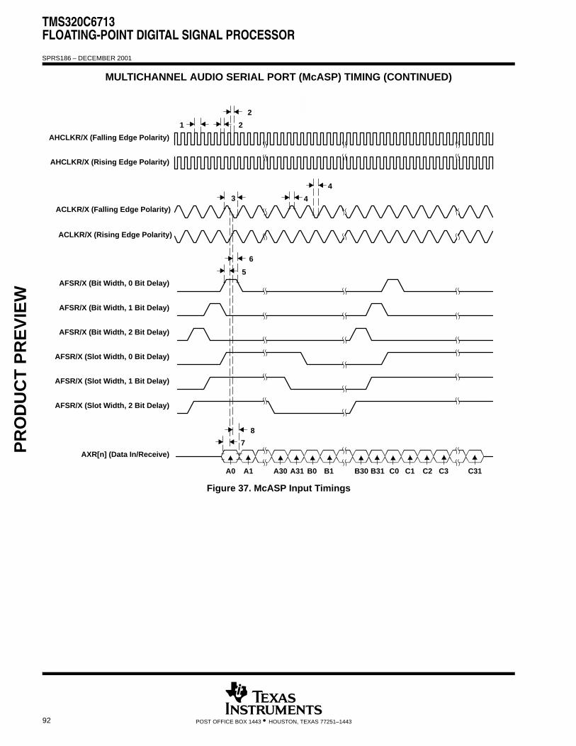
TMS320C6713FLOATING-POINT DIGITAL SIGNAL PROCESSOR
SPRS186 – DECEMBER 2001
92 POST OFFICE BOX 1443 • HOUSTON, TEXAS 77251–1443
MULTICHANNEL AUDIO SERIAL PORT (McASP) TIMING (CONTINUED)
8
7
4
43
2
21
A0 A1 B0 B1A30 A31 B30 B31 C0 C1 C2 C3 C31
AHCLKR/X (Falling Edge Polarity)
AHCLKR/X (Rising Edge Polarity)
ACLKR/X (Falling Edge Polarity)
ACLKR/X (Rising Edge Polarity)
AFSR/X (Bit Width, 0 Bit Delay)
AFSR/X (Bit Width, 1 Bit Delay)
AFSR/X (Bit Width, 2 Bit Delay)
AFSR/X (Slot Width, 0 Bit Delay)
AFSR/X (Slot Width, 1 Bit Delay)
AFSR/X (Slot Width, 2 Bit Delay)
AXR[n] (Data In/Receive)
6
5
Figure 37. McASP Input Timings
PR
OD
UC
T P
RE
VIE
W

TMS320C6713FLOATING-POINT DIGITAL SIGNAL PROCESSOR
SPRS186 – DECEMBER 2001
93POST OFFICE BOX 1443 • HOUSTON, TEXAS 77251–1443
MULTICHANNEL AUDIO SERIAL PORT (McASP) TIMING (CONTINUED)
1615
151515
15
15
14
131313
1313
1313
12
1211
1010
9
A0 A1 B0 B1A30 A31 B30 B31 C0 C1 C2 C3 C31
AHCLKR/X (Falling Edge Polarity)
AHCLKR/X (Rising Edge Polarity)
ACLKR/X (Falling Edge Polarity)
ACLKR/X (Rising Edge Polarity)
AFSR/X (Bit Width, 0 Bit Delay)
AFSR/X (Bit Width, 1 Bit Delay)
AFSR/X (Bit Width, 2 Bit Delay)
AFSR/X (Slot Width, 0 Bit Delay)
AFSR/X (Slot Width, 1 Bit Delay)
AFSR/X (Slot Width, 2 Bit Delay)
AXR[n] (Data Out/Transmit)
Figure 38. McASP Output Timings
PR
OD
UC
T P
RE
VIE
W

TMS320C6713FLOATING-POINT DIGITAL SIGNAL PROCESSOR
SPRS186 – DECEMBER 2001
94 POST OFFICE BOX 1443 • HOUSTON, TEXAS 77251–1443
INTER-INTEGRATED CIRCUITS (I2C) TIMING
switching characteristics for I2C timings† (see Figure 39)
–150–225
NO. STANDARDMODE
FASTMODE
UNIT
MIN MAX MIN MAX
1 tc(SCL) Cycle time, SCL
2 tw(SCLL) Pulse duration, SCL low
3 tw(SCLH) Pulse duration, SCL high
4 tsu(SCLH-SDAL)Setup time, SCL high before SDA low (for a repeated START condi-tion)
5 th(SCLL-SDAL) Hold time, SCL low after SDA low (for a repeated START condition)
6 tsu(SDA-SDLH) Setup time, SDA valid before SCL high
7 th(SDA SDLL)Hold time, SDA valid after For CBUS compatible masters
7 th(SDA-SDLL)Hold time, SDA valid afterSCL low For I2C bus devices
8 tw(SDAH) Pulse duration, SDA high between STOP and START conditions
9 tr(SDA) Rise time, SDA
10 tr(SCL) Rise time, SCL
11 tf(SDA) Fall time, SDA
12 tf(SCL) Fall time, SCL
13 tsu(SCLH-SDAH) Setup time, SCL high before SDA high (for STOP condition)
14 tw(SP) Pulse duration, spike (must be suppressed)
15 Cb§ Capacitive load for each bus line
† The I2C pins SDA and SCL do not feature fail-safe I/O buffers. These pins could potentially draw current when the device is powered down.‡ The maximum th(SCLL-SDAL) has only to be met if the device does not stretch the low period (tw(SCLL)) of the SCL signal.§ Cb = The total capacitance of one bus line in pF.
Stop Start RepeatedStart
Stop
SDA
SCL
82
6 14
10 3 13
1
57
1254
NOTES: A. A device must internally provide a hold time of at least 300 ns for the SDA signal (referred to the VIHmin of the SCL signal) to bridgethe undefined region of the falling edge of SCL.
B. The maximum th(SCLL–SDAL) has only to be met if the device does not stretch the LOW period (tw(SCLL)) of the SCL signal.C. A Fast-mode I2C-bus device can be used in a Standard-mode I2C-bus system, but the requirement tsu(SDA–SDLH) • 250 ns must
then be met. This will automatically be the case if the device does not stretch the LOW period of the SCL signal. If such a devicedoes stretch the LOW period of the SCL signal, it must output the next data bit to the SDA line tr max + tsu(SDA–SDLH) = 1000 + 250 =1250 ns (according to the standard-mode I2C-bus specification) before the SCL line is released.
D. Cb = total capacitance of one bus line in pF. If mixed with fast-mode devices, faster fall-times are allowed
Figure 39. I2C Timings
PR
OD
UC
T P
RE
VIE
W

TMS320C6713FLOATING-POINT DIGITAL SIGNAL PROCESSOR
SPRS186 – DECEMBER 2001
95POST OFFICE BOX 1443 • HOUSTON, TEXAS 77251–1443
HOST-PORT INTERFACE TIMING
timing requirements for host-port interface cycles†‡ (see Figure 40, Figure 41, Figure 42, andFigure 43)
NO.
–150–225 UNITNO.
MIN MAXUNIT
1 tsu(SELV-HSTBL) Setup time, select signals§ valid before HSTROBE low
2 th(HSTBL-SELV) Hold time, select signals§ valid after HSTROBE low
3 tw(HSTBL) Pulse duration, HSTROBE low
4 tw(HSTBH) Pulse duration, HSTROBE high between consecutive accesses
10 tsu(SELV-HASL) Setup time, select signals§ valid before HAS low
11 th(HASL-SELV) Hold time, select signals§ valid after HAS low
12 tsu(HDV-HSTBH) Setup time, host data valid before HSTROBE high
13 th(HSTBH-HDV) Hold time, host data valid after HSTROBE high
14 th(HRDYL-HSTBL)Hold time, HSTROBE low after HRDY low. HSTROBE should not be inactivated
until HRDY is active (low); otherwise, HPI writes will not complete properly.
18 tsu(HASL-HSTBL) Setup time, HAS low before HSTROBE low
19 th(HSTBL-HASL) Hold time, HAS low after HSTROBE low
† HSTROBE refers to the following logical operation on HCS, HDS1, and HDS2: [NOT(HDS1 XOR HDS2)] OR HCS.‡ P = 1/CPU clock frequency in ns. For example, when running parts at 225 MHz, use P = 4.4 ns.§ Select signals include: HCNTL[1:0], HR/W, and HHWIL.
switching characteristics over recommended operating conditions during host-port interfacecycles†‡ (see Figure 40, Figure 41, Figure 42, and Figure 43)
NO. PARAMETER
–150–225 UNITNO. PARAMETER
MIN MAXUNIT
5 td(HCS-HRDY) Delay time, HCS to HRDY¶
6 td(HSTBL-HRDYH) Delay time, HSTROBE low to HRDY high#
7 td(HSTBL-HDLZ) Delay time, HSTROBE low to HD low impedance for an HPI read
8 td(HDV-HRDYL) Delay time, HD valid to HRDY low
9 toh(HSTBH-HDV) Output hold time, HD valid after HSTROBE high
15 td(HSTBH-HDHZ) Delay time, HSTROBE high to HD high impedance
16 td(HSTBL-HDV) Delay time, HSTROBE low to HD valid
17 td(HSTBH-HRDYH) Delay time, HSTROBE high to HRDY high||
20 td(HASL-HRDYH) Delay time, HAS low to HRDY high
† HSTROBE refers to the following logical operation on HCS, HDS1, and HDS2: [NOT(HDS1 XOR HDS2)] OR HCS.‡ P = 1/CPU clock frequency in ns. For example, when running parts at 225 MHz, use P = 4.4 ns.¶ HCS enables HRDY, and HRDY is always low when HCS is high. The case where HRDY goes high when HCS falls indicates that HPI is busy
completing a previous HPID write or READ with autoincrement.# This parameter is used during an HPID read. At the beginning of the first half-word transfer on the falling edge of HSTROBE, the HPI sends the
request to the EDMA internal address generation hardware, and HRDY remains high until the EDMA internal address generation hardware loadsthe requested data into HPID.
|| This parameter is used after the second half-word of an HPID write or autoincrement read. HRDY remains low if the access is not an HPID writeor autoincrement read. Reading or writing to HPIC or HPIA does not affect the HRDY signal.
PR
OD
UC
T P
RE
VIE
W

TMS320C6713FLOATING-POINT DIGITAL SIGNAL PROCESSOR
SPRS186 – DECEMBER 2001
96 POST OFFICE BOX 1443 • HOUSTON, TEXAS 77251–1443
HOST-PORT INTERFACE TIMING (CONTINUED)
1st halfword 2nd halfword
51786
51785
15916
1597
43
21
21
21
21
21
21
HAS
HCNTL[1:0]
HR/W
HHWIL
HSTROBE†
HCS
HD[15:0] (output)
HRDY (case 1)
HRDY (case 2)
3
† HSTROBE refers to the following logical operation on HCS, HDS1, and HDS2: [NOT(HDS1 XOR HDS2)] OR HCS.
Figure 40. HPI Read Timing (HAS Not Used, Tied High)
HAS†
HCNTL[1:0]
HR/W
HHWIL
HSTROBE‡
HCS
HD[15:0] (output)
HRDY (case 1)
HRDY (case 2)
1st half-word 2nd half-word
517820
51785
15916
1597
43
11
1011
10
1110
1110
111011
1019 19
1818
† For correct operation, strobe the HAS signal only once per HSTROBE active cycle.‡ HSTROBE refers to the following logical operation on HCS, HDS1, and HDS2: [NOT(HDS1 XOR HDS2)] OR HCS.
Figure 41. HPI Read Timing (HAS Used)
PR
OD
UC
T P
RE
VIE
W

TMS320C6713FLOATING-POINT DIGITAL SIGNAL PROCESSOR
SPRS186 – DECEMBER 2001
97POST OFFICE BOX 1443 • HOUSTON, TEXAS 77251–1443
HOST-PORT INTERFACE TIMING (CONTINUED)
1st halfword 2nd halfword 517
5
1312
1312
414
3
21
21
21
21
21
21
HAS
HCNTL[1:0]
HR/W
HHWIL
HSTROBE†
HCS
HD[15:0] (input)
HRDY
3
† HSTROBE refers to the following logical operation on HCS, HDS1, and HDS2: [NOT(HDS1 XOR HDS2)] OR HCS.
Figure 42. HPI Write Timing (HAS Not Used, Tied High)
1st half-word 2nd half-word 5175
1312
1312
414
3
1110
1110
1110
1110
1110
1110
HAS†
HCNTL[1:0]
HR/W
HHWIL
HSTROBE‡
HCS
HD[15:0] (input)
HRDY
1919
18 18
† For correct operation, strobe the HAS signal only once per HSTROBE active cycle.‡ HSTROBE refers to the following logical operation on HCS, HDS1, and HDS2: [NOT(HDS1 XOR HDS2)] OR HCS.
Figure 43. HPI Write Timing (HAS Used)
PR
OD
UC
T P
RE
VIE
W

TMS320C6713FLOATING-POINT DIGITAL SIGNAL PROCESSOR
SPRS186 – DECEMBER 2001
98 POST OFFICE BOX 1443 • HOUSTON, TEXAS 77251–1443
MULTICHANNEL BUFFERED SERIAL PORT TIMING
timing requirements for McBSP†‡ (see Figure 44)
NO.
–150–225 UNITNO.
MIN MAXUNIT
2 tc(CKRX) Cycle time, CLKR/X CLKR/X ext
3 tw(CKRX) Pulse duration, CLKR/X high or CLKR/X low CLKR/X ext
5 t Setup time external FSR high before CLKR lowCLKR int
5 tsu(FRH-CKRL) Setup time, external FSR high before CLKR lowCLKR ext
6 t Hold time external FSR high after CLKR lowCLKR int
6 th(CKRL-FRH) Hold time, external FSR high after CLKR lowCLKR ext
7 t Setup time DR valid before CLKR lowCLKR int
7 tsu(DRV-CKRL) Setup time, DR valid before CLKR lowCLKR ext
8 t Hold time DR valid after CLKR lowCLKR int
8 th(CKRL-DRV) Hold time, DR valid after CLKR lowCLKR ext
10 t Setup time external FSX high before CLKX lowCLKX int
10 tsu(FXH-CKXL) Setup time, external FSX high before CLKX lowCLKX ext
11 t Hold time external FSX high after CLKX lowCLKX int
11 th(CKXL-FXH) Hold time, external FSX high after CLKX lowCLKX ext
† CLKRP = CLKXP = FSRP = FSXP = 0. If polarity of any of the signals is inverted, then the timing references of that signal are also inverted.‡ P = 1/CPU clock frequency in ns. For example, when running parts at 225 MHz, use P = 4.4 ns.§ The minimum CLKR/X period is twice the CPU cycle time (2P). This means that the maximum bit rate for communications between the McBSP
and other device is 75 Mbps for 150 MHz CPU clock or 50 Mbps for 100 MHz CPU clock; where the McBSP is either the master or the slave.Care must be taken to ensure that the AC timings specified in this data sheet are met. The maximum bit rate for McBSP-to-McBSPcommunications is 33 Mbps; therefore, the minimum CLKR/X clock cycle is either twice the CPU cycle time (2P), or 30 ns (33 MHz), whichevervalue is larger. For example, when running parts at 150 MHz (P = 6.7 ns), use 33 ns as the minimum CLKR/X clock cycle (by setting the appropriateCLKGDV ratio or external clock source). When running parts at 60 MHz (P = 16.67 ns), use 2P = 33 ns (30 MHz) as the minimum CLKR/X clockcycle. The maximum bit rate for McBSP-to-McBSP communications applies when the serial port is a master of the clock and frame syncs (withCLKR connected to CLKX, FSR connected to FSX, CLKXM = FSXM = 1, and CLKRM = FSRM = 0) in data delay 1 or 2 mode (R/XDATDLY =01b or 10b) and the other device the McBSP communicates to is a slave.
PR
OD
UC
T P
RE
VIE
W

TMS320C6713FLOATING-POINT DIGITAL SIGNAL PROCESSOR
SPRS186 – DECEMBER 2001
99POST OFFICE BOX 1443 • HOUSTON, TEXAS 77251–1443
MULTICHANNEL BUFFERED SERIAL PORT TIMING (CONTINUED)
switching characteristics over recommended operating conditions for McBSP†‡ (see Figure 44)
NO. PARAMETER
–150–225 UNITNO. PARAMETER
MIN MAXUNIT
1 td(CKSH-CKRXH)Delay time, CLKS high to CLKR/X high for internal CLKR/X generated fromCLKS input
2 tc(CKRX) Cycle time, CLKR/X CLKR/X int
3 tw(CKRX) Pulse duration, CLKR/X high or CLKR/X low CLKR/X int
4 td(CKRH-FRV) Delay time, CLKR high to internal FSR valid CLKR int
9 t Delay time CLKX high to internal FSX validCLKX int
9 td(CKXH-FXV) Delay time, CLKX high to internal FSX validCLKX ext
12 tDisable time, DX high impedance following last data bit CLKX int
12 tdis(CKXH-DXHZ)Disable time, DX high im edance following last data bitfrom CLKX high CLKX ext
13 t Delay time CLKX high to DX validCLKX int
13 td(CKXH-DXV) Delay time, CLKX high to DX validCLKX ext
14 t
Delay time, FSX high to DX valid FSX int
14 td(FXH-DXV) ONLY applies when in datadelay 0 (XDATDLY = 00b) mode FSX ext
† CLKRP = CLKXP = FSRP = FSXP = 0. If polarity of any of the signals is inverted, then the timing references of that signal are also inverted.‡ Minimum delay times also represent minimum output hold times.§ P = 1/CPU clock frequency in ns. For example, when running parts at 225 MHz, use P = 4.4 ns.¶ The minimum CLKR/X period is twice the CPU cycle time (2P). This means that the maximum bit rate for communications between the McBSP
and other device is 75 Mbps for 150 MHz CPU clock or 50 Mbps for 100 MHz CPU clock; where the McBSP is either the master or the slave.Care must be taken to ensure that the AC timings specified in this data sheet are met. The maximum bit rate for McBSP-to-McBSPcommunications is 33 Mbps; therefore, the minimum CLKR/X clock cycle is either twice the CPU cycle time (2P), or 30 ns (33 MHz), whichevervalue is larger. For example, when running parts at 150 MHz (P = 6.7 ns), use 33 ns as the minimum CLKR/X clock cycle (by setting the appropriateCLKGDV ratio or external clock source). When running parts at 60 MHz (P = 16.67 ns), use 2P = 33 ns (30 MHz) as the minimum CLKR/X clockcycle. The maximum bit rate for McBSP-to-McBSP communications applies when the serial port is a master of the clock and frame syncs (withCLKR connected to CLKX, FSR connected to FSX, CLKXM = FSXM = 1, and CLKRM = FSRM = 0) in data delay 1 or 2 mode (R/XDATDLY =01b or 10b) and the other device the McBSP communicates to is a slave.
# C = H or LS = sample rate generator input clock = 2P if CLKSM = 1 (P = 1/CPU clock frequency)
= sample rate generator input clock = P_clks if CLKSM = 0 (P_clks = CLKS period)H = CLKX high pulse width = (CLKGDV/2 + 1) * S if CLKGDV is even
= (CLKGDV + 1)/2 * S if CLKGDV is odd or zeroL = CLKX low pulse width = (CLKGDV/2) * S if CLKGDV is even
= (CLKGDV + 1)/2 * S if CLKGDV is odd or zeroCLKGDV should be set appropriately to ensure the McBSP bit rate does not exceed the maximum limit (see ¶ footnote above).
|| Extra delay from CLKX high to DX valid applies only to the first data bit of a device, if and only if DXENA = 1 in SPCR.If DXENA = 0, then D1 = D2 = 0If DXENA = 1, then D1 = 2P, D2 = 4P
PR
OD
UC
T P
RE
VIE
W

TMS320C6713FLOATING-POINT DIGITAL SIGNAL PROCESSOR
SPRS186 – DECEMBER 2001
100 POST OFFICE BOX 1443 • HOUSTON, TEXAS 77251–1443
MULTICHANNEL BUFFERED SERIAL PORT TIMING (CONTINUED)
Bit(n-1) (n-2) (n-3)
Bit 0 Bit(n-1) (n-2) (n-3)
141312
1110
9
33
2
87
65
44
3
1
32
CLKS
CLKR
FSR (int)
FSR (ext)
DR
CLKX
FSX (int)
FSX (ext)
FSX (XDATDLY=00b)
DX
13
Figure 44. McBSP Timings
PR
OD
UC
T P
RE
VIE
W

TMS320C6713FLOATING-POINT DIGITAL SIGNAL PROCESSOR
SPRS186 – DECEMBER 2001
101POST OFFICE BOX 1443 • HOUSTON, TEXAS 77251–1443
MULTICHANNEL BUFFERED SERIAL PORT TIMING (CONTINUED)
timing requirements for FSR when GSYNC = 1 (see Figure 45)
NO.
–150–225 UNITNO.
MIN MAXUNIT
1 tsu(FRH-CKSH) Setup time, FSR high before CLKS high
2 th(CKSH-FRH) Hold time, FSR high after CLKS high
21
CLKS
FSR external
CLKR/X (no need to resync)
CLKR/X (needs resync)
Figure 45. FSR Timing When GSYNC = 1
PR
OD
UC
T P
RE
VIE
W

TMS320C6713FLOATING-POINT DIGITAL SIGNAL PROCESSOR
SPRS186 – DECEMBER 2001
102 POST OFFICE BOX 1443 • HOUSTON, TEXAS 77251–1443
MULTICHANNEL BUFFERED SERIAL PORT TIMING (CONTINUED)
timing requirements for McBSP as SPI master or slave: CLKSTP = 10b, CLKXP = 0†‡ (see Figure 46)
NO
–150–225
UNITNO.MASTER SLAVE
UNIT
MIN MAX MIN MAX
4 tsu(DRV-CKXL) Setup time, DR valid before CLKX low
5 th(CKXL-DRV) Hold time, DR valid after CLKX low
† P = 1/CPU clock frequency in ns. For example, when running parts at 225 MHz, use P = 4.4 ns.‡ For all SPI slave modes, CLKG is programmed as 1/2 of the CPU clock by setting CLKSM = CLKGDV = 1.
switching characteristics over recommended operating conditions for McBSP as SPI master orslave: CLKSTP = 10b, CLKXP = 0†‡ (see Figure 46)
NO PARAMETER
–150–225
UNITNO. PARAMETERMASTER§ SLAVE
UNIT
MIN MAX MIN MAX
1 th(CKXL-FXL) Hold time, FSX low after CLKX low¶
2 td(FXL-CKXH) Delay time, FSX low to CLKX high#
3 td(CKXH-DXV) Delay time, CLKX high to DX valid
6 tdis(CKXL-DXHZ)Disable time, DX high impedance following last data bit fromCLKX low
7 tdis(FXH-DXHZ)Disable time, DX high impedance following last data bit fromFSX high
8 td(FXL-DXV) Delay time, FSX low to DX valid
† P = 1/CPU clock frequency in ns. For example, when running parts at 225 MHz, use P = 4.4 ns.‡ For all SPI slave modes, CLKG is programmed as 1/2 of the CPU clock by setting CLKSM = CLKGDV = 1.§ S = Sample rate generator input clock = 2P if CLKSM = 1 (P = 1/CPU clock frequency)
= Sample rate generator input clock = P_clks if CLKSM = 0 (P_clks = CLKS period)T = CLKX period = (1 + CLKGDV) * SH = CLKX high pulse width = (CLKGDV/2 + 1) * S if CLKGDV is even
= (CLKGDV + 1)/2 * S if CLKGDV is odd or zeroL = CLKX low pulse width = (CLKGDV/2) * S if CLKGDV is even
= (CLKGDV + 1)/2 * S if CLKGDV is odd or zero¶ FSRP = FSXP = 1. As a SPI master, FSX is inverted to provide active-low slave-enable output. As a slave, the active-low signal input on FSX
and FSR is inverted before being used internally.CLKXM = FSXM = 1, CLKRM = FSRM = 0 for master McBSPCLKXM = CLKRM = FSXM = FSRM = 0 for slave McBSP
# FSX should be low before the rising edge of clock to enable slave devices and then begin a SPI transfer at the rising edge of the master clock(CLKX).
PR
OD
UC
T P
RE
VIE
W
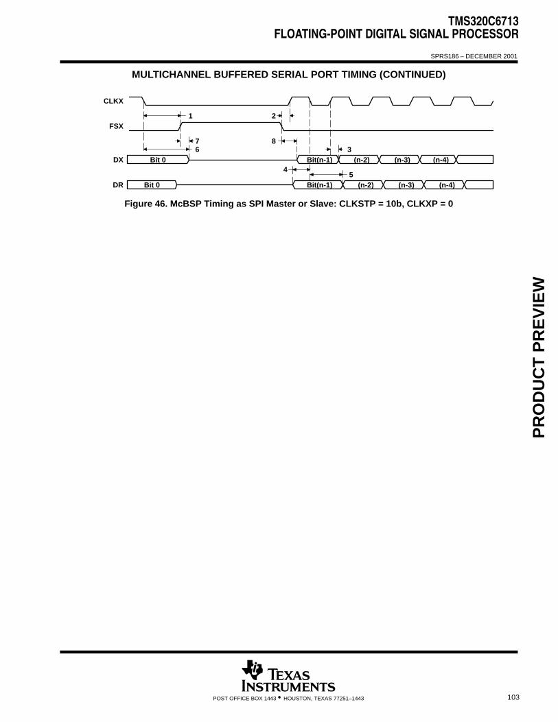
TMS320C6713FLOATING-POINT DIGITAL SIGNAL PROCESSOR
SPRS186 – DECEMBER 2001
103POST OFFICE BOX 1443 • HOUSTON, TEXAS 77251–1443
MULTICHANNEL BUFFERED SERIAL PORT TIMING (CONTINUED)
Bit 0 Bit(n-1) (n-2) (n-3) (n-4)
Bit 0 Bit(n-1) (n-2) (n-3) (n-4)5
4
387
6
21
CLKX
FSX
DX
DR
Figure 46. McBSP Timing as SPI Master or Slave: CLKSTP = 10b, CLKXP = 0
PR
OD
UC
T P
RE
VIE
W

TMS320C6713FLOATING-POINT DIGITAL SIGNAL PROCESSOR
SPRS186 – DECEMBER 2001
104 POST OFFICE BOX 1443 • HOUSTON, TEXAS 77251–1443
MULTICHANNEL BUFFERED SERIAL PORT TIMING (CONTINUED)
timing requirements for McBSP as SPI master or slave: CLKSTP = 11b, CLKXP = 0†‡ (see Figure 47)
NO
–150–225
UNITNO.MASTER SLAVE
UNIT
MIN MAX MIN MAX
4 tsu(DRV-CKXH) Setup time, DR valid before CLKX high
5 th(CKXH-DRV) Hold time, DR valid after CLKX high
† P = 1/CPU clock frequency in ns. For example, when running parts at 225 MHz, use P = 4.4 ns.‡ For all SPI slave modes, CLKG is programmed as 1/2 of the CPU clock by setting CLKSM = CLKGDV = 1.
switching characteristics over recommended operating conditions for McBSP as SPI master orslave: CLKSTP = 11b, CLKXP = 0†‡ (see Figure 47)
NO PARAMETER
–150–225
UNITNO. PARAMETERMASTER§ SLAVE
UNIT
MIN MAX MIN MAX
1 th(CKXL-FXL) Hold time, FSX low after CLKX low¶
2 td(FXL-CKXH) Delay time, FSX low to CLKX high#
3 td(CKXL-DXV) Delay time, CLKX low to DX valid
6 tdis(CKXL-DXHZ)Disable time, DX high impedance following last data bit fromCLKX low
7 td(FXL-DXV) Delay time, FSX low to DX valid
† P = 1/CPU clock frequency in ns. For example, when running parts at 225 MHz, use P = 4.4 ns.‡ For all SPI slave modes, CLKG is programmed as 1/2 of the CPU clock by setting CLKSM = CLKGDV = 1.§ S = Sample rate generator input clock = 2P if CLKSM = 1 (P = 1/CPU clock frequency)
= Sample rate generator input clock = P_clks if CLKSM = 0 (P_clks = CLKS period)T = CLKX period = (1 + CLKGDV) * SH = CLKX high pulse width = (CLKGDV/2 + 1) * S if CLKGDV is even
= (CLKGDV + 1)/2 * S if CLKGDV is odd or zeroL = CLKX low pulse width = (CLKGDV/2) * S if CLKGDV is even
= (CLKGDV + 1)/2 * S if CLKGDV is odd or zero¶ FSRP = FSXP = 1. As a SPI master, FSX is inverted to provide active-low slave-enable output. As a slave, the active-low signal input on FSX
and FSR is inverted before being used internally.CLKXM = FSXM = 1, CLKRM = FSRM = 0 for master McBSPCLKXM = CLKRM = FSXM = FSRM = 0 for slave McBSP
# FSX should be low before the rising edge of clock to enable slave devices and then begin a SPI transfer at the rising edge of the master clock(CLKX).
Bit 0 Bit(n-1) (n-2) (n-3) (n-4)
Bit 0 Bit(n-1) (n-2) (n-3) (n-4)
4
376
21
CLKX
FSX
DX
DR
5
Figure 47. McBSP Timing as SPI Master or Slave: CLKSTP = 11b, CLKXP = 0
PR
OD
UC
T P
RE
VIE
W
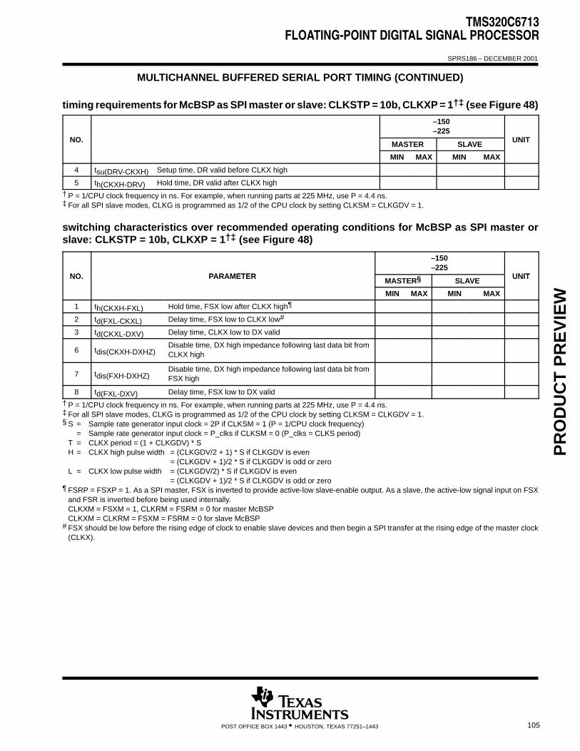
TMS320C6713FLOATING-POINT DIGITAL SIGNAL PROCESSOR
SPRS186 – DECEMBER 2001
105POST OFFICE BOX 1443 • HOUSTON, TEXAS 77251–1443
MULTICHANNEL BUFFERED SERIAL PORT TIMING (CONTINUED)
timing requirements for McBSP as SPI master or slave: CLKSTP = 10b, CLKXP = 1†‡ (see Figure 48)
NO
–150–225
UNITNO.MASTER SLAVE
UNIT
MIN MAX MIN MAX
4 tsu(DRV-CKXH) Setup time, DR valid before CLKX high
5 th(CKXH-DRV) Hold time, DR valid after CLKX high
† P = 1/CPU clock frequency in ns. For example, when running parts at 225 MHz, use P = 4.4 ns.‡ For all SPI slave modes, CLKG is programmed as 1/2 of the CPU clock by setting CLKSM = CLKGDV = 1.
switching characteristics over recommended operating conditions for McBSP as SPI master orslave: CLKSTP = 10b, CLKXP = 1†‡ (see Figure 48)
NO PARAMETER
–150–225
UNITNO. PARAMETERMASTER§ SLAVE
UNIT
MIN MAX MIN MAX
1 th(CKXH-FXL) Hold time, FSX low after CLKX high¶
2 td(FXL-CKXL) Delay time, FSX low to CLKX low#
3 td(CKXL-DXV) Delay time, CLKX low to DX valid
6 tdis(CKXH-DXHZ)Disable time, DX high impedance following last data bit fromCLKX high
7 tdis(FXH-DXHZ)Disable time, DX high impedance following last data bit fromFSX high
8 td(FXL-DXV) Delay time, FSX low to DX valid
† P = 1/CPU clock frequency in ns. For example, when running parts at 225 MHz, use P = 4.4 ns.‡ For all SPI slave modes, CLKG is programmed as 1/2 of the CPU clock by setting CLKSM = CLKGDV = 1.§ S = Sample rate generator input clock = 2P if CLKSM = 1 (P = 1/CPU clock frequency)
= Sample rate generator input clock = P_clks if CLKSM = 0 (P_clks = CLKS period)T = CLKX period = (1 + CLKGDV) * SH = CLKX high pulse width = (CLKGDV/2 + 1) * S if CLKGDV is even
= (CLKGDV + 1)/2 * S if CLKGDV is odd or zeroL = CLKX low pulse width = (CLKGDV/2) * S if CLKGDV is even
= (CLKGDV + 1)/2 * S if CLKGDV is odd or zero¶ FSRP = FSXP = 1. As a SPI master, FSX is inverted to provide active-low slave-enable output. As a slave, the active-low signal input on FSX
and FSR is inverted before being used internally.CLKXM = FSXM = 1, CLKRM = FSRM = 0 for master McBSPCLKXM = CLKRM = FSXM = FSRM = 0 for slave McBSP
# FSX should be low before the rising edge of clock to enable slave devices and then begin a SPI transfer at the rising edge of the master clock(CLKX).
PR
OD
UC
T P
RE
VIE
W

TMS320C6713FLOATING-POINT DIGITAL SIGNAL PROCESSOR
SPRS186 – DECEMBER 2001
106 POST OFFICE BOX 1443 • HOUSTON, TEXAS 77251–1443
MULTICHANNEL BUFFERED SERIAL PORT TIMING (CONTINUED)
Bit 0 Bit(n-1) (n-2) (n-3) (n-4)
Bit 0 Bit(n-1) (n-2) (n-3) (n-4)54
387
6
21
CLKX
FSX
DX
DR
Figure 48. McBSP Timing as SPI Master or Slave: CLKSTP = 10b, CLKXP = 1
PR
OD
UC
T P
RE
VIE
W

TMS320C6713FLOATING-POINT DIGITAL SIGNAL PROCESSOR
SPRS186 – DECEMBER 2001
107POST OFFICE BOX 1443 • HOUSTON, TEXAS 77251–1443
MULTICHANNEL BUFFERED SERIAL PORT TIMING (CONTINUED)
timing requirements for McBSP as SPI master or slave: CLKSTP = 11b, CLKXP = 1†‡ (see Figure 49)
NO
–150–225
UNITNO.MASTER SLAVE
UNIT
MIN MAX MIN MAX
4 tsu(DRV-CKXH) Setup time, DR valid before CLKX high
5 th(CKXH-DRV) Hold time, DR valid after CLKX high
† P = 1/CPU clock frequency in ns. For example, when running parts at 225 MHz, use P = 4.4 ns.‡ For all SPI slave modes, CLKG is programmed as 1/2 of the CPU clock by setting CLKSM = CLKGDV = 1.
switching characteristics over recommended operating conditions for McBSP as SPI master orslave: CLKSTP = 11b, CLKXP = 1†‡ (see Figure 49)
NO PARAMETER
–150–225
UNITNO. PARAMETERMASTER§ SLAVE
UNIT
MIN MAX MIN MAX
1 th(CKXH-FXL) Hold time, FSX low after CLKX high¶
2 td(FXL-CKXL) Delay time, FSX low to CLKX low#
3 td(CKXH-DXV) Delay time, CLKX high to DX valid
6 tdis(CKXH-DXHZ)Disable time, DX high impedance following last data bit fromCLKX high
7 td(FXL-DXV) Delay time, FSX low to DX valid
† P = 1/CPU clock frequency in ns. For example, when running parts at 225 MHz, use P = 4.4 ns.‡ For all SPI slave modes, CLKG is programmed as 1/2 of the CPU clock by setting CLKSM = CLKGDV = 1.§ S = Sample rate generator input clock = 2P if CLKSM = 1 (P = 1/CPU clock frequency)
= Sample rate generator input clock = P_clks if CLKSM = 0 (P_clks = CLKS period)T = CLKX period = (1 + CLKGDV) * SH = CLKX high pulse width = (CLKGDV/2 + 1) * S if CLKGDV is even
= (CLKGDV + 1)/2 * S if CLKGDV is odd or zeroL = CLKX low pulse width = (CLKGDV/2) * S if CLKGDV is even
= (CLKGDV + 1)/2 * S if CLKGDV is odd or zero¶ FSRP = FSXP = 1. As a SPI master, FSX is inverted to provide active-low slave-enable output. As a slave, the active-low signal input on FSX
and FSR is inverted before being used internally.CLKXM = FSXM = 1, CLKRM = FSRM = 0 for master McBSPCLKXM = CLKRM = FSXM = FSRM = 0 for slave McBSP
# FSX should be low before the rising edge of clock to enable slave devices and then begin a SPI transfer at the rising edge of the master clock(CLKX).
PR
OD
UC
T P
RE
VIE
W

TMS320C6713FLOATING-POINT DIGITAL SIGNAL PROCESSOR
SPRS186 – DECEMBER 2001
108 POST OFFICE BOX 1443 • HOUSTON, TEXAS 77251–1443
MULTICHANNEL BUFFERED SERIAL PORT TIMING (CONTINUED)
Bit 0 Bit(n-1) (n-2) (n-3) (n-4)
Bit 0 Bit(n-1) (n-2) (n-3) (n-4)54
376
21
CLKX
FSX
DX
DR
Figure 49. McBSP Timing as SPI Master or Slave: CLKSTP = 11b, CLKXP = 1
PR
OD
UC
T P
RE
VIE
W

TMS320C6713FLOATING-POINT DIGITAL SIGNAL PROCESSOR
SPRS186 – DECEMBER 2001
109POST OFFICE BOX 1443 • HOUSTON, TEXAS 77251–1443
TIMER TIMING
timing requirements for timer inputs† (see Figure 50)
NO.
–150–225 UNITNO.
MIN MAXUNIT
1 tw(TINPH) Pulse duration, TINP high
2 tw(TINPL) Pulse duration, TINP low
† P = 1/CPU clock frequency in ns. For example, when running parts at 225 MHz, use P = 4.4 ns.
switching characteristics over recommended operating conditions for timer outputs†(see Figure 50)
NO. PARAMETER
–150–225 UNITNO. PARAMETER
MIN MAXUNIT
3 tw(TOUTH) Pulse duration, TOUT high
4 tw(TOUTL) Pulse duration, TOUT low
† P = 1/CPU clock frequency in ns. For example, when running parts at 225 MHz, use P = 4.4 ns.
TINPx
TOUTx
4
3
21
Figure 50. Timer Timing
PR
OD
UC
T P
RE
VIE
W

TMS320C6713FLOATING-POINT DIGITAL SIGNAL PROCESSOR
SPRS186 – DECEMBER 2001
110 POST OFFICE BOX 1443 • HOUSTON, TEXAS 77251–1443
GENERAL-PURPOSE INPUT/OUTPUT (GPIO) PORT TIMING
timing requirements for GPIO inputs† (see Figure 51)
NO.
–150–225 UNITNO.
MIN MAXUNIT
1 tw(GPIH) Pulse duration, GPIx high
2 tw(GPIL) Pulse duration, GPIx low
† P = 1/CPU clock frequency in ns. For example, when running parts at 225 MHz, use P = 4.4 ns.
switching characteristics over recommended operating conditions for GPIO outputs† (see Figure 51)
NO. PARAMETER
–150–225 UNITNO. PARAMETER
MIN MAXUNIT
3 tw(GPOH) Pulse duration, GPOx high
4 tw(GPOL) Pulse duration, GPOx low
† P = 1/CPU clock frequency in ns. For example, when running parts at 225 MHz, use P = 4.4 ns.
GPIx
GPOx
4
3
21
Figure 51. GPIO Port Timing
PR
OD
UC
T P
RE
VIE
W
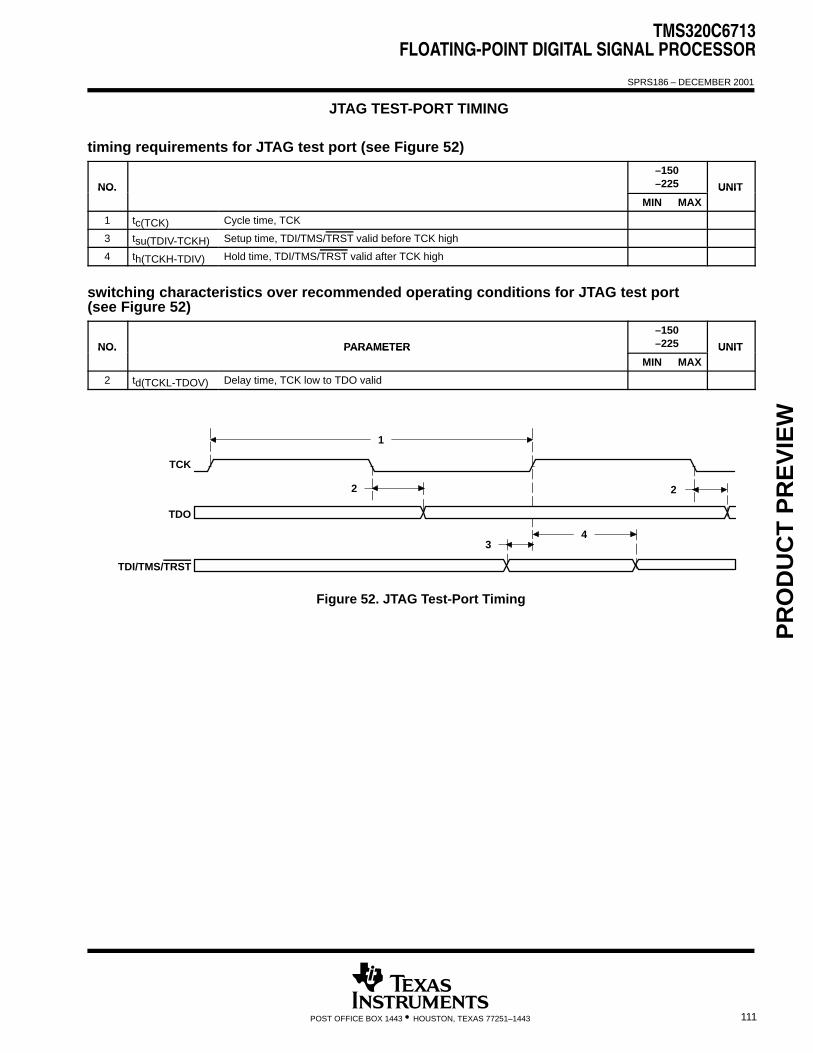
TMS320C6713FLOATING-POINT DIGITAL SIGNAL PROCESSOR
SPRS186 – DECEMBER 2001
111POST OFFICE BOX 1443 • HOUSTON, TEXAS 77251–1443
JTAG TEST-PORT TIMING
timing requirements for JTAG test port (see Figure 52)
NO.
–150–225 UNITNO.
MIN MAXUNIT
1 tc(TCK) Cycle time, TCK
3 tsu(TDIV-TCKH) Setup time, TDI/TMS/TRST valid before TCK high
4 th(TCKH-TDIV) Hold time, TDI/TMS/TRST valid after TCK high
switching characteristics over recommended operating conditions for JTAG test port(see Figure 52)
NO. PARAMETER
–150–225 UNITNO. PARAMETER
MIN MAXUNIT
2 td(TCKL-TDOV) Delay time, TCK low to TDO valid
TCK
TDO
TDI/TMS/TRST
1
2
34
2
Figure 52. JTAG Test-Port Timing
PR
OD
UC
T P
RE
VIE
W
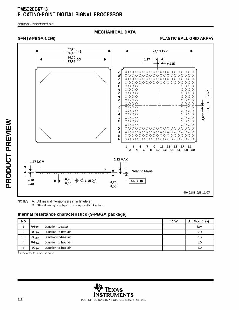
TMS320C6713FLOATING-POINT DIGITAL SIGNAL PROCESSOR
SPRS186 – DECEMBER 2001
112 POST OFFICE BOX 1443 • HOUSTON, TEXAS 77251–1443
MECHANICAL DATA GFN (S-PBGA-N256) PLASTIC BALL GRID ARRAY
0,635
1915 1713119
Y
V
TU
PN
R
W
75
L
JK
H
FG
31
D
BC
A
E
M
24,13 TYP
Seating Plane
4040185-2/B 11/97
10 12 14 16 18 208642
27,20
23,9524,70
SQ
SQ26,80
0,900,60
0,500,70
0,63
51,
27
0,15
1,27
M0,15
2,32 MAX
0,400,30
1,17 NOM
NOTES: A. All linear dimensions are in millimeters.B. This drawing is subject to change without notice.
thermal resistance characteristics (S-PBGA package)
NO °C/W Air Flow (m/s)†
1 RΘJC Junction-to-case N/A
2 RΘJA Junction-to-free air 0.0
3 RΘJA Junction-to-free air 0.5
4 RΘJA Junction-to-free air 1.0
5 RΘJA Junction-to-free air 2.0
† m/s = meters per second
PR
OD
UC
T P
RE
VIE
W

TMS320C6713FLOATING-POINT DIGITAL SIGNAL PROCESSOR
SPRS186 – DECEMBER 2001
113POST OFFICE BOX 1443 • HOUSTON, TEXAS 77251–1443
MECHANICAL DATA PYP (S-PQFP-G208) PowerPAD PLASTIC QUAD FLATPACK
0,13 NOM
105
Thermal Pad(See Note D)
104
0,17
53
0,27
0,25
0,450,75
0,150,05
52
Seating Plane
4146966/A 12/97
Gage Plane
157
208
156
SQ
SQ
28,05
29,9030,10
27,95
25,50 TYP
1
1,451,35
1,60 MAX 0,08
0,50
M0,08
0°–7°
NOTES: A. All linear dimensions are in millimeters.B. This drawing is subject to change without notice.C. Body dimensions include mold flash or protrusions.D. The package thermal performance may be enhanced by bonding the thermal pad to an external thermal plane.
This pad is electrically and thermally connected to the backside of the die and possibly selected leads.E. Falls within JEDEC MS-026
PowerPAD is a trademark of Texas Instruments.
PR
OD
UC
T P
RE
VIE
W

TMS320C6713FLOATING-POINT DIGITAL SIGNAL PROCESSOR
SPRS186 – DECEMBER 2001
114 POST OFFICE BOX 1443 • HOUSTON, TEXAS 77251–1443
MECHANICAL DATA (CONTINUED)
thermal resistance characteristics (S-PQFP-G208 package)
NO °C/W Air Flow (m/s)†
1 RΘJC Junction-to-case N/A
2 RΘJA Junction-to-free air 0.0
3 RΘJA Junction-to-free air 0.5
4 RΘJA Junction-to-free air 1.0
5 RΘJA Junction-to-free air 2.0
† m/s = meters per second
PR
OD
UC
T P
RE
VIE
W

IMPORTANT NOTICE
Texas Instruments Incorporated and its subsidiaries (TI) reserve the right to make corrections, modifications,enhancements, improvements, and other changes to its products and services at any time and to discontinueany product or service without notice. Customers should obtain the latest relevant information before placingorders and should verify that such information is current and complete. All products are sold subject to TI’s termsand conditions of sale supplied at the time of order acknowledgment.
TI warrants performance of its hardware products to the specifications applicable at the time of sale inaccordance with TI’s standard warranty. Testing and other quality control techniques are used to the extent TIdeems necessary to support this warranty. Except where mandated by government requirements, testing of allparameters of each product is not necessarily performed.
TI assumes no liability for applications assistance or customer product design. Customers are responsible fortheir products and applications using TI components. To minimize the risks associated with customer productsand applications, customers should provide adequate design and operating safeguards.
TI does not warrant or represent that any license, either express or implied, is granted under any TI patent right,copyright, mask work right, or other TI intellectual property right relating to any combination, machine, or processin which TI products or services are used. Information published by TI regarding third–party products or servicesdoes not constitute a license from TI to use such products or services or a warranty or endorsement thereof.Use of such information may require a license from a third party under the patents or other intellectual propertyof the third party, or a license from TI under the patents or other intellectual property of TI.
Reproduction of information in TI data books or data sheets is permissible only if reproduction is withoutalteration and is accompanied by all associated warranties, conditions, limitations, and notices. Reproductionof this information with alteration is an unfair and deceptive business practice. TI is not responsible or liable forsuch altered documentation.
Resale of TI products or services with statements different from or beyond the parameters stated by TI for thatproduct or service voids all express and any implied warranties for the associated TI product or service andis an unfair and deceptive business practice. TI is not responsible or liable for any such statements.
Mailing Address:
Texas InstrumentsPost Office Box 655303Dallas, Texas 75265
Copyright 2001, Texas Instruments Incorporated