TMS320C6713 DSK Technical Reference
52
TMS320C6713 DSK 2003 DSP Development Systems Reference Technical
Transcript of TMS320C6713 DSK Technical Reference
TMS320C6713 DSK
2003 DSP Development Systems
ReferenceTechnical

TMS320C6713 DSK Technical Reference
506735-0001 Rev. A May 2003
SPECTRUM DIGITAL, INC.12502 Exchange Drive, Suite 440 Stafford, TX. 77477
Tel: 281.494.4505 Fax: [email protected] www.spectrumdigital.com

IMPORTANT NOTICE
Spectrum Digital, Inc. reserves the right to make changes to its products or to discontinue anyproduct or service without notice. Customers are advised to obtain the latest version of relevantinformation to verify that the data being relied on is current before placing orders.
Spectrum Digital, Inc. warrants performance of its products and related software to currentspecifications in accordance with Spectrum Digital’s standard warranty. Testing and other qualitycontrol techniques are utilized to the extent deemed necessary to support this warranty.
Please be aware that the products described herein are not intended for use in life-support appliances, devices, or systems. Spectrum Digital does not warrant nor is Spectrum Digital liable for the product described herein to be used in other than a development environment.
Spectrum Digital, Inc. assumes no liability for applications assistance, customer product design, software performance, or infringement of patents or services described herein. Nor does SpectrumDigital warrant or represent any license, either express or implied, is granted under any patent right,copyright, or other intellectual property right of Spectrum Digital, Inc. covering or relating to anycombination, machine, or process in which such Digital Signal Processing development products orservices might be or are used.
WARNING
This equipment is intended for use in a laboratory test environment only. It generates, uses, and canradiate radio frequency energy and has not been tested for compliance with the limits of computingdevices pursuant to subpart J of part 15 of FCC rules, which are designed to provide reasonableprotection against radio frequency interference. Operation of this equipment in other environmentsmay cause interference with radio communications, in which case the user at his own expense will berequired to take whatever measures necessary to correct this interference.
Copyright © 2003 Spectrum Digital, Inc.

Contents
1 Introduction to the TMS320C6713 DSK Module . . . . . . . . . . . . . . . . . . . . . . . . . . . . . . . 1-1 Provides you with a description of the TMS320C6713 DSK Module, key features, and block diagram. 1.1 Key Features . . . . . . . . . . . . . . . . . . . . . . . . . . . . . . . . . . . . . . . . . . . . . . . . . . . . . . . . . . 1-2 1.2 Functional Overview . . . . . . . . . . . . . . . . . . . . . . . . . . . . . . . . . . . . . . . . . . . . . . . . . . . . 1-3 1.3 Basic Operation . . . . . . . . . . . . . . . . . . . . . . . . . . . . . . . . . . . . . . . . . . . . . . . . . . . . . . . . . 1-4 1.4 Memory Map . . . . . . . . . . . . . . . . . . . . . . . . . . . . . . . . . . . . . . . . . . . . . . . . . . . . . . . . . . 1-5 1.5 Configuration Switch Settings . . . . . . . . . . . . . . . . . . . . . . . . . . . . . . . . . . . . . . . . . . . . . 1-6 1.6 Power Supply . . . . . . . . . . . . . . . . . . . . . . . . . . . . . . . . . . . . . . . . . . . . . . . . . . . . . . . . . 1-62 Board Components . . . . . . . . . . . . . . . . . . . . . . . . . . . . . . . . . . . . . . . . . . . . . . . . . . . . . . . . 2-1 Describes the operation of the major board components on the TMS320C6713 DSK. 2.1 CPLD (programmable Logic) . . . . . . . . . . . . . . . . . . . . . . . . . . . . . . . . . . . . . . . . . . . 2-2 2.1.1 CPLD Overview . . . . . . . . . . . . . . . . . . . . . . . . . . . . . . . . . . . . . . . . . . . . . . . . . . . . 2-2 2.1.2 CPLD Registers . . . . . . . . . . . . . . . . . . . . . . . . . . . . . . . . . . . . . . . . . . . . . . . . . . . . . 2-3 2.1.3 USER_REG Register . . . . . . . . . . . . . . . . . . . . . . . . . . . . . . . . . . . . . . . . . . . . . . 2-3 2.1.4 DC_REG Register . . . . . . . . . . . . . . . . . . . . . . . . . . . . . . . . . . . . . . . . . . . . . . . . . . 2-4 2.1.5 Version Register . . . . . . . . . . . . . . . . . . . . . . . . . . . . . . . . . . . . . . . . . . . . . . . . . . 2-4 2.1.6 MISC Register . . . . . . . . . . . . . . . . . . . . . . . . . . . . . . . . . . . . . . . . . . . . . . . . . . . . . 2-5 2.2 Codec Interface . . . . . . . . . . . . . . . . . . . . . . . . . . . . . . . . . . . . . . . . . . . . . . . . . . . . . 2-6 2.3 SRAM Interface . . . . . . . . . . . . . . . . . . . . . . . . . . . . . . . . . . . . . . . . . . . . . . . . . . . . . 2-7 2.4 Flash ROM Interface . . . . . . . . . . . . . . . . . . . . . . . . . . . . . . . . . . . . . . . . . . . . . . . . 2-7 2.5 LEDs and DIP Switches . . . . . . . . . . . . . . . . . . . . . . . . . . . . . . . . . . . . . . . . . . . . . . 2-7 2.6 Daughter Card Interface . . . . . . . . . . . . . . . . . . . . . . . . . . . . . . . . . . . . . . . . . . . . . . 2-83 Physical Specifications . . . . . . . . . . . . . . . . . . . . . . . . . . . . . . . . . . . . . . . . . . . . . . . . . . . . 3-1 Describes the physical layout of the TMS320C6713 DSK and its connectors. 3.1 Board Layout . . . . . . . . . . . . . . . . . . . . . . . . . . . . . . . . . . . . . . . . . . . . . . . . . . . . . . . . 3-2 3.2 Connector Index . . . . . . . . . . . . . . . . . . . . . . . . . . . . . . . . . . . . . . . . . . . . . . . . . . . . 3-3 3.3 Expansion Connectors . . . . . . . . . . . . . . . . . . . . . . . . . . . . . . . . . . . . . . . . . . . . . . . . 3-3 3.3.1 J4, Memory Expansion . . . . . . . . . . . . . . . . . . . . . . . . . . . . . . . . . . . . . . . . . . . . . 3-4 3.3.2 J3, Peripheral Expansion . . . . . . . . . . . . . . . . . . . . . . . . . . . . . . . . . . . . . . . . . . . . 3-5 3.3.3 J1, HPI Expansion Connector . . . . . . . . . . . . . . . . . . . . . . . . . . . . . . . . . . . . . . . . 3-6 3.4 Audio Connectors . . . . . . . . . . . . . . . . . . . . . . . . . . . . . . . . . . . . . . . . . . . . . . . . . . . . . 3-7 3.4.1 J301, Microphone Connector . . . . . . . . . . . . . . . . . . . . . . . . . . . . . . . . . . . . . . . . . 3-7 3.4.2 J303, Audio Line In Connector . . . . . . . . . . . . . . . . . . . . . . . . . . . . . . . . . . . . . . . . 3-7 3.4.3 J304, Audio Line Out Connector . . . . . . . . . . . . . . . . . . . . . . . . . . . . . . . . . . . . . . 3-8 3.4.4 J302, Headphone Connector . . . . . . . . . . . . . . . . . . . . . . . . . . . . . . . . . . . . . . . . . . 3-8 3.5 Power Connectors . . . . . . . . . . . . . . . . . . . . . . . . . . . . . . . . . . . . . . . . . . . . . . . . . . . . . 3-9 3.5.1 J5, +5V Main Power Connector . . . . . . . . . . . . . . . . . . . . . . . . . . . . . . . . . . . . . . . 3-9 3.5.2 J6, Optional Power Connector . . . . . . . . . . . . . . . . . . . . . . . . . . . . . . . . . . . . . . . . . 3-9 3.6. Miscellaneous Connectors . . . . . . . . . . . . . . . . . . . . . . . . . . . . . . . . . . . . . . . . . . . 3-10

3.6.1 J201, USB Port . . . . . . . . . . . . . . . . . . . . . . . . . . . . . . . . . . . . . . . . . . . . . . . . . . . . 3-10 3.6.2 J8, External JTAG Connector . . . . . . . . . . . . . . . . . . . . . . . . . . . . . . . . . . . . . . . . 3-10 3.6.3 JP3, PLD Programming Connector . . . . . . . . . . . . . . . . . . . . . . . . . . . . . . . . . . . . . 3-11 3.7 System LEDs . . . . . . . . . . . . . . . . . . . . . . . . . . . . . . . . . . . . . . . . . . . . . . . . . . . . . . . 3-11 3.8 Reset Switch . . . . . . . . . . . . . . . . . . . . . . . . . . . . . . . . . . . . . . . . . . . . . . . . . . . . . . . 3-11A Schematics . . . . . . . . . . . . . . . . . . . . . . . . . . . . . . . . . . . . . . . . . . . . . . . . . . . . . . . . . . . . . . A-1 Contains the schematics for the TMS320C6713 DSKB Mechanical Information . . . . . . . . . . . . . . . . . . . . . . . . . . . . . . . . . . . . . . . . . . . . . . . . . . B-1 Contains the mechanical information about the TMS320C6713 DSK
About This Manual
This document describes the board level operations of the TMS320C6713 DSPStarter Kit (DSK) module. The DSK is based on the Texas Instruments TMS320C6713 Digital Signal Processor.
The TMS320C6713 DSK is a table top card to allow engineers and softwaredevelopers to evaluate certain characteristics of the TMS320C6713 DSP to determineif the processor meets the designers application requirements. Evaluators can createsoftware to execute onboard or expand the system in a variety of ways.
Notational Conventions
This document uses the following conventions.
The TMS320C6713 DSK will sometimes be referred to as the DSK.
Program listings, program examples, and interactive displays are shown is a specialitalic typeface. Here is a sample program listing.
equations!rd = !strobe&rw;
Information About Cautions
This book may contain cautions.This is an example of a caution statement.A caution statement describes a situation that could potentially damage your software,or hardware, or other equipment. The information in a caution is provided for yourprotection. Please read each caution carefully.
Related Documents
Texas Instruments TMS320C67xx DSP CPU Reference GuideTexas Instruments TMS320C67xx DSP Peripherals Reference Guide

Table 1: Manual History
Revision History
A Alpha Release

1-1
Chapter 1
Introduction to the TMS320C6713 DSK
Chapter One provides a description of the TMS320C6713 DSK alongwith the key features and a block diagram of the circuit board.
Topic Page
1.1 Key Features 1-21.2 Functional Overview 1-31.3 Basic Operation 1-41.4 Memory Map 1-51.5 Configuration Switch Settings 1-61.6 Power Supply 1-6
Spectrum Digital, Inc
1-2 TMS320C6713 DSK Module Technical Reference
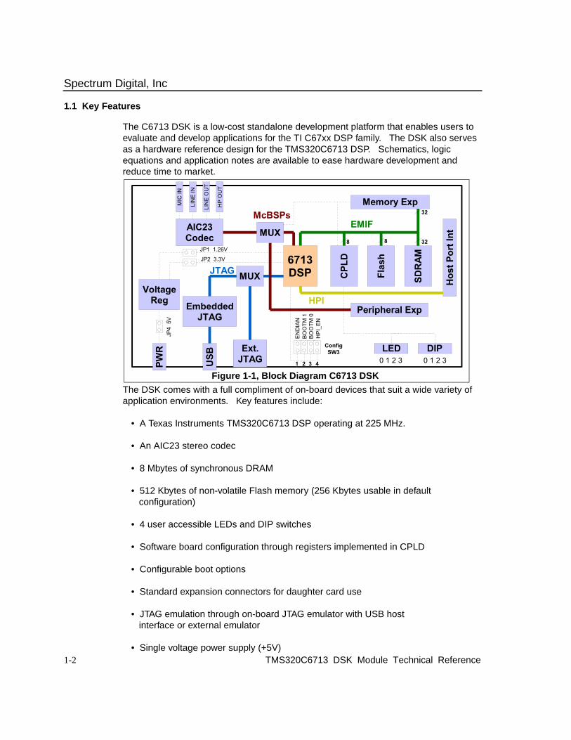
1.1 Key Features
The C6713 DSK is a low-cost standalone development platform that enables users toevaluate and develop applications for the TI C67xx DSP family. The DSK also servesas a hardware reference design for the TMS320C6713 DSP. Schematics, logicequations and application notes are available to ease hardware development andreduce time to market.
The DSK comes with a full compliment of on-board devices that suit a wide variety ofapplication environments. Key features include:
• A Texas Instruments TMS320C6713 DSP operating at 225 MHz.
• An AIC23 stereo codec
• 8 Mbytes of synchronous DRAM
• 512 Kbytes of non-volatile Flash memory (256 Kbytes usable in default configuration)
• 4 user accessible LEDs and DIP switches
• Software board configuration through registers implemented in CPLD
• Configurable boot options
• Standard expansion connectors for daughter card use
• JTAG emulation through on-board JTAG emulator with USB host interface or external emulator
• Single voltage power supply (+5V)
Figure 1-1, Block Diagram C6713 DSK
Ext.JTAG
AIC23Codec
Hos
t Por
t Int
MUX
MUX
MIC
IN
LIN
E O
UT
HP
OU
T
LIN
E IN
Peripheral Exp
LED DIP
EMIF
HPI
McBSPs
JTAG
0 1 2 30 1 2 3
CPL
D
Memory Exp
PWR
USB
EmbeddedJTAG
JP1 1.26V
JP2 3.3V
END
IAN
BOO
TM 1
BOO
TM 0
6713DSP
SDR
AM
328
Flas
h
8
1 32
ConfigSW3
32
HPI
_EN
4
VoltageReg
JP4
5V

Spectrum Digital, Inc
1-3
1.2 Functional Overview of the TMS320C6713 DSK
The DSP on the 6713 DSK interfaces to on-board peripherals through a 32-bit wideEMIF (External Memory InterFace). The SDRAM, Flash and CPLD are all connectedto the bus. EMIF signals are also connected daughter card expansion connectorswhich are used for third party add-in boards.
The DSP interfaces to analog audio signals through an on-board AIC23 codec and four3.5 mm audio jacks (microphone input, line input, line output, and headphone output).The codec can select the microphone or the line input as the active input. The analogoutput is driven to both the line out (fixed gain) and headphone (adjustable gain)connectors. McBSP0 is used to send commands to the codec control interface whileMcBSP1 is used for digital audio data. McBSP0 and McBSP1 can be re-routed to theexpansion connectors in software.
A programmable logic device called a CPLD is used to implement glue logic that tiesthe board components together. The CPLD has a register based user interface thatlets the user configure the board by reading and writing to its registers.
The DSK includes 4 LEDs and a 4 position DIP switch as a simple way to provide theuser with interactive feedback. Both are accessed by reading and writing to the CPLDregisters.
An included 5V external power supply is used to power the board. On-board switchingvoltage regulators provide the +1.26V DSP core voltage and +3.3V I/O supplies. Theboard is held in reset until these supplies are within operating specifications.
Code Composer communicates with the DSK through an embedded JTAG emulatorwith a USB host interface. The DSK can also be used with an external emulatorthrough the external JTAG connector.
Spectrum Digital, Inc
1-4 TMS320C6713 DSK Module Technical Reference
1.3 Basic Operation
The DSK is designed to work with TI’s Code Composer Studio developmentenvironment and ships with a version specifically tailored to work with the board.Code Composer communicates with the board through the on-board JTAG emulator.To start, follow the instructions in the Quick Start Guide to install Code Composer. This process will install all of the necessary development tools, documentation anddrivers.
After the install is complete, follow these steps to run Code Composer. The DSK mustbe fully connected to launch the DSK version of Code Composer.
1) Connect the included power supply to the DSK.
2) Connect the DSK to your PC with a standard USB cable (also included).
3) Launch Code Composer from its icon on your desktop.
Detailed information about the DSK including a tutorial, examples and referencematerial is available in the DSK’s help file. You can access the help file through CodeComposer’s help menu. It can also be launched directly by double-clicking on the filec6713dsk.hlp in Code Composer’s docs\hlp subdirectory.

Spectrum Digital, Inc
1-5
1.4 Memory Map
The C67xx family of DSPs has a large byte addressable address space. Program codeand data can be placed anywhere in the unified address space. Addresses are always32-bits wide.
The memory map shows the address space of a generic 6713 processor on the leftwith specific details of how each region is used on the right. By default, the internalmemory sits at the beginning of the address space. Portions of the internal memorycan be reconfigured in software as L2 cache rather than fixed RAM.
The EMIF has 4 separate addressable regions called chip enable spaces (CE0-CE3). The SDRAM occupies CE0 while the Flash and CPLD share CE1. CE2 and CE3 aregenerally reserved for daughtercards.
Figure 1-2, Memory Map, C6713 DSK
Internal Memory
Reserved Spaceor
Peripheral Regs
AddressC67x Family
Memory Type
SDRAM
CPLDFlash
DaughterCard
6713 DSK
InternalMemory
Reservedor
Peripheral
EMIF CE0
EMIF CE3
EMIF CE2
EMIF CE1
0x80000000
0x90000000
0xA0000000
0xB0000000
0x00000000
0x00030000
0x90080000
Spectrum Digital, Inc
1-6 TMS320C6713 DSK Module Technical Reference
1.5 Configuration Switch Settings
The DSK has 4 configuration switches that allows users to control the operational stateof the DSP when it is released from reset. The configuration switch block is labeledSW3 on the DSK board, next to the reset switch.
Configuration switch 1 controls the endianness of the DSP while switches 2 and 3configure the boot mode that will be used when the DSP starts executing. Configuration switch 4 controls the on-chip multiplexing of HPI and McASP signalsbrought out to the HPI expansion connector. By default all switches are off whichcorresponds to EMIF boot (out of 8-bit Flash) in little endian mode and HPI signals onthe HPI expansion connector.
1.6 Power Supply
The DSK operates from a single +5V external power supply connected to the mainpower input (J5). Internally, the +5V input is converted into +1.26V and +3.3V usingseparate voltage regulators. The +1.26V supply is used for the DSP core while the+3.3V supply is used for the DSP's I/O buffers and all other chips on the board. Thepower connector is a 2.5mm barrel-type plug.
There are three power test points on the DSK at JP1, JP2 and JP4. All I/O currentpasses through JP2 while all core current passes through JP1. All system currentpasses through JP4. Normally these jumpers are closed. To measure the currentpassing through remove the jumpers and connect the pins with a current measuringdevice such as a multimeter or current probe.
It is possible to provide the daughter card with +12V and -12V when the external powerconnector (J6) is used.
Table 1: Configuration Switch Settings
Switch 1 Switch 2 Switch 3 Switch 4 Configuration Description
Off Little endian (default)
On Big endian
Off Off EMIF boot from 8-bit Flash (default)
Off On HPI/Emulation boot
On Off 32-bit EMIF boot
On On 16-bit EMIF boot
Off HPI enabled on HPI pins (default)
On McASP1 enabled on HPI pins
2-1
Chapter 2
Board Components
This chapter describes the operation of the major board components onthe TMS320C6713 DSK.
Topic Page
2.1 CPLD (Programmable Logic) 2-22.1.1 CPLD Overview 2-22.1.2 CPLD Registers 2-32.1.3 USER_REG Register 2-32.1.4 DC_REG Register 2-42.1.5 Version Register 2-42.1.6 MISC Register 2-52.2 AIC23 Codec 2-62.3 Sychronous DRAM 2-72.4 Flash Memory 2-72.5 LEDs and DIP Switches 2-72.6 Daughter Card Interface 2-8
Spectrum Digital, Inc
2-2 TMS320C6713 DSK Module Technical Reference
2.1 CPLD (Programmable Logic)
The C6713 DSK uses an Altera EPM3128TC100-10 Complex Programmable LogicDevice (CPLD) device to implement:
• 4 Memory-mapped control/status registers that allow software control of various board features.
• Control of the daughter card interface and signals.
• Assorted "glue" logic that ties the board components together.
2.1.1 CPLD Overview
The CPLD logic is used to implement functionality specific to the DSK. Your ownhardware designs will likely implement a completely different set of functions or takeadvantage of the DSPs high level of integration for system design and avoid the use of external logic completely.
The CPLD implements simple random logic functions that eliminate the need foradditional discrete devices. In particular, the CPLD aggregates the various resetsignals coming from the reset button and power supervisors and generates a globalreset.
The EPM3128TC100-10 is a 3.3V (5V tolerant), 100-pin QFP device that provides 128 macrocells, 80 I/O pins, and a 10 ns pin-to-pin delay. The device is EEPROM-based and is in-system programmable via a dedicated JTAG interface (a 10-pin header on the DSK). The CPLD source files are written in the industrystandard VHDL (Hardware Design Language) and included with the DSK.
Spectrum Digital, Inc
2-3
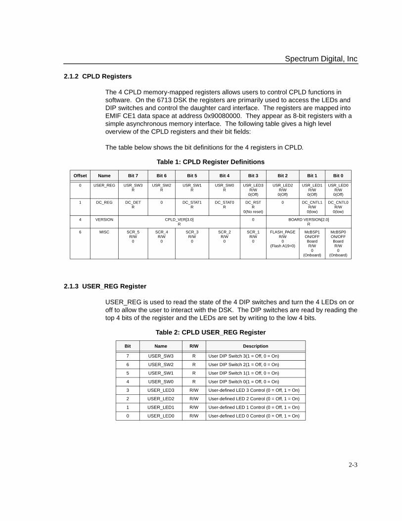
2.1.2 CPLD Registers
The 4 CPLD memory-mapped registers allows users to control CPLD functions insoftware. On the 6713 DSK the registers are primarily used to access the LEDs andDIP switches and control the daughter card interface. The registers are mapped intoEMIF CE1 data space at address 0x90080000. They appear as 8-bit registers with asimple asynchronous memory interface. The following table gives a high leveloverview of the CPLD registers and their bit fields:
The table below shows the bit definitions for the 4 registers in CPLD.
2.1.3 USER_REG Register
USER_REG is used to read the state of the 4 DIP switches and turn the 4 LEDs on oroff to allow the user to interact with the DSK. The DIP switches are read by reading thetop 4 bits of the register and the LEDs are set by writing to the low 4 bits.
Table 1: CPLD Register Definitions
Offset Name Bit 7 Bit 6 Bit 5 Bit 4 Bit 3 Bit 2 Bit 1 Bit 0
0 USER_REG USR_SW3R
USR_SW2R
USR_SW1R
USR_SW0R
USR_LED3R/W
0(Off)
USR_LED2R/W
0(Off)
USR_LED1R/W
0(Off)
USR_LED0R/W
0(Off)
1 DC_REG DC_DETR
0 DC_STAT1R
DC_STAT0R
DC_RSTR
0(No reset)
0 DC_CNTL1R/W
0(low)
DC_CNTL0R/W
0(low)
4 VERSION CPLD_VER[3.0]R
0 BOARD VERSION[2.0]R
6 MISC SCR_5R/W
0
SCR_4R/W
0
SCR_3R/W
0
SCR_2R/W
0
SCR_1R/W
0
FLASH_PAGER/W
0(Flash A19=0)
McBSP1ON/OFFBoardR/W
0(Onboard)
McBSP0ON/OFFBoardR/W
0(Onboard)
Table 2: CPLD USER_REG Register
Bit Name R/W Description
7 USER_SW3 R User DIP Switch 3(1 = Off, 0 = On)
6 USER_SW2 R User DIP Switch 2(1 = Off, 0 = On)
5 USER_SW1 R User DIP Switch 1(1 = Off, 0 = On)
4 USER_SW0 R User DIP Switch 0(1 = Off, 0 = On)
3 USER_LED3 R/W User-defined LED 3 Control (0 = Off, 1 = On)
2 USER_LED2 R/W User-defined LED 2 Control (0 = Off, 1 = On)
1 USER_LED1 R/W User-defined LED 1 Control (0 = Off, 1 = On)
0 USER_LED0 R/W User-defined LED 0 Control (0 = Off, 1 = On)
Spectrum Digital, Inc
2-4 TMS320C6713 DSK Module Technical Reference
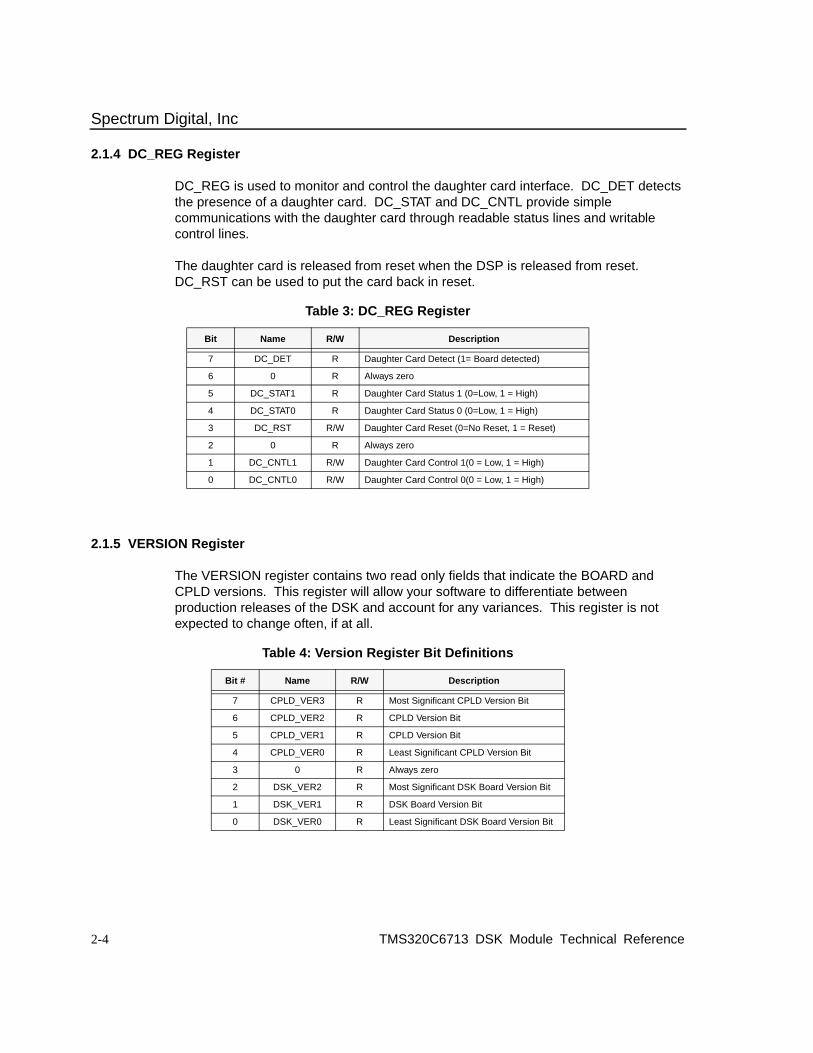
2.1.4 DC_REG Register
DC_REG is used to monitor and control the daughter card interface. DC_DET detectsthe presence of a daughter card. DC_STAT and DC_CNTL provide simplecommunications with the daughter card through readable status lines and writablecontrol lines.
The daughter card is released from reset when the DSP is released from reset. DC_RST can be used to put the card back in reset.
2.1.5 VERSION Register
The VERSION register contains two read only fields that indicate the BOARD andCPLD versions. This register will allow your software to differentiate betweenproduction releases of the DSK and account for any variances. This register is notexpected to change often, if at all.
Table 3: DC_REG Register
Bit Name R/W Description
7 DC_DET R Daughter Card Detect (1= Board detected)
6 0 R Always zero
5 DC_STAT1 R Daughter Card Status 1 (0=Low, 1 = High)
4 DC_STAT0 R Daughter Card Status 0 (0=Low, 1 = High)
3 DC_RST R/W Daughter Card Reset (0=No Reset, 1 = Reset)
2 0 R Always zero
1 DC_CNTL1 R/W Daughter Card Control 1(0 = Low, 1 = High)
0 DC_CNTL0 R/W Daughter Card Control 0(0 = Low, 1 = High)
Table 4: Version Register Bit Definitions
Bit # Name R/W Description
7 CPLD_VER3 R Most Significant CPLD Version Bit
6 CPLD_VER2 R CPLD Version Bit
5 CPLD_VER1 R CPLD Version Bit
4 CPLD_VER0 R Least Significant CPLD Version Bit
3 0 R Always zero
2 DSK_VER2 R Most Significant DSK Board Version Bit
1 DSK_VER1 R DSK Board Version Bit
0 DSK_VER0 R Least Significant DSK Board Version Bit
Spectrum Digital, Inc
2-5
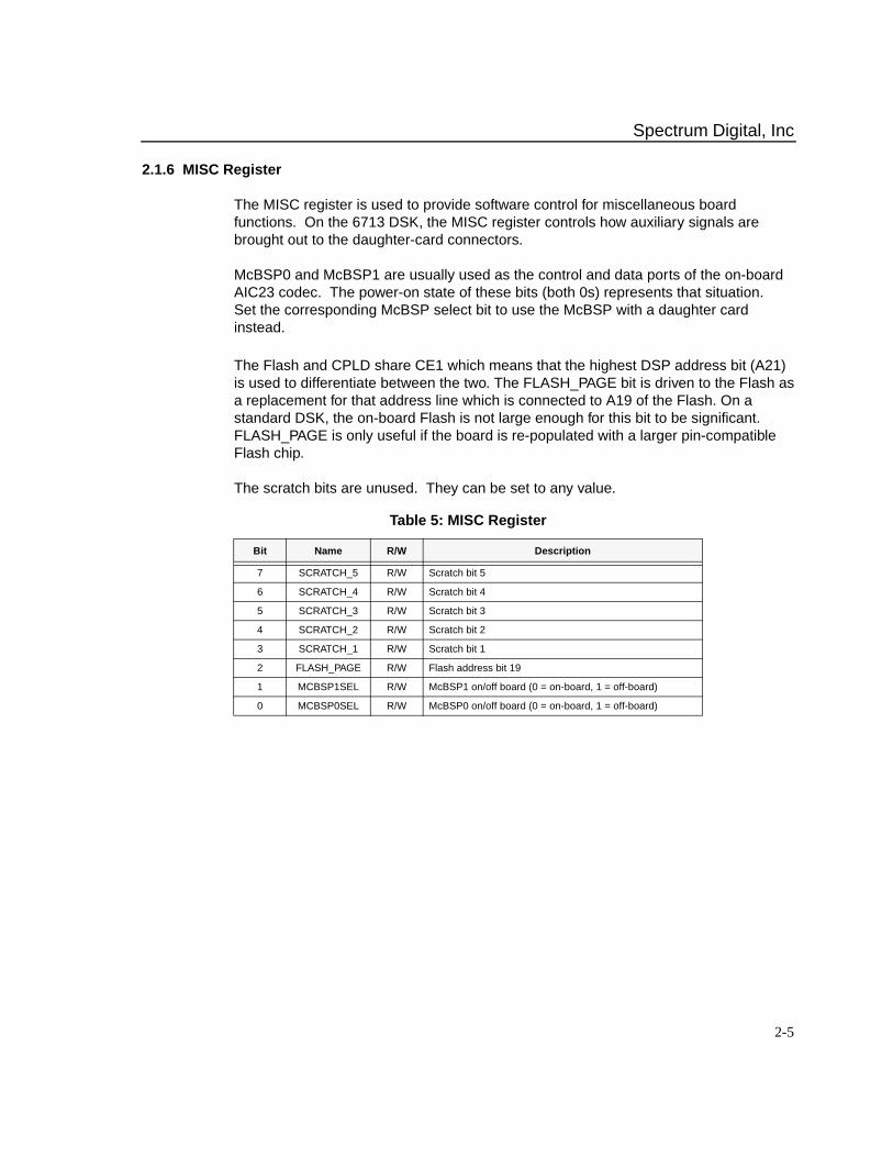
2.1.6 MISC Register
The MISC register is used to provide software control for miscellaneous boardfunctions. On the 6713 DSK, the MISC register controls how auxiliary signals arebrought out to the daughter-card connectors.
McBSP0 and McBSP1 are usually used as the control and data ports of the on-boardAIC23 codec. The power-on state of these bits (both 0s) represents that situation. Set the corresponding McBSP select bit to use the McBSP with a daughter cardinstead.
The Flash and CPLD share CE1 which means that the highest DSP address bit (A21)is used to differentiate between the two. The FLASH_PAGE bit is driven to the Flash asa replacement for that address line which is connected to A19 of the Flash. On astandard DSK, the on-board Flash is not large enough for this bit to be significant.FLASH_PAGE is only useful if the board is re-populated with a larger pin-compatibleFlash chip.
The scratch bits are unused. They can be set to any value.
Table 5: MISC Register
Bit Name R/W Description
7 SCRATCH_5 R/W Scratch bit 5
6 SCRATCH_4 R/W Scratch bit 4
5 SCRATCH_3 R/W Scratch bit 3
4 SCRATCH_2 R/W Scratch bit 2
3 SCRATCH_1 R/W Scratch bit 1
2 FLASH_PAGE R/W Flash address bit 19
1 MCBSP1SEL R/W McBSP1 on/off board (0 = on-board, 1 = off-board)
0 MCBSP0SEL R/W McBSP0 on/off board (0 = on-board, 1 = off-board)
Spectrum Digital, Inc
2-6 TMS320C6713 DSK Module Technical Reference
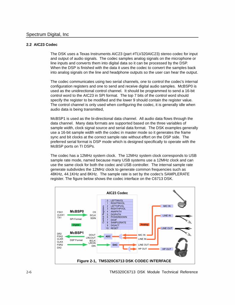
2.2 AIC23 Codec
The DSK uses a Texas Instruments AIC23 (part #TLV320AIC23) stereo codec for inputand output of audio signals. The codec samples analog signals on the microphone orline inputs and converts them into digital data so it can be processed by the DSP. When the DSP is finished with the data it uses the codec to convert the samples backinto analog signals on the line and headphone outputs so the user can hear the output.
The codec communicates using two serial channels, one to control the codec’s internalconfiguration registers and one to send and receive digital audio samples. McBSP0 isused as the unidirectional control channel. It should be programmed to send a 16-bitcontrol word to the AIC23 in SPI format. The top 7 bits of the control word shouldspecify the register to be modified and the lower 9 should contain the register value. The control channel is only used when configuring the codec, it is generally idle whenaudio data is being transmitted,
McBSP1 is used as the bi-directional data channel. All audio data flows through thedata channel. Many data formats are supported based on the three variables ofsample width, clock signal source and serial data format. The DSK examples generallyuse a 16-bit sample width with the codec in master mode so it generates the framesync and bit clocks at the correct sample rate without effort on the DSP side. Thepreferred serial format is DSP mode which is designed specifically to operate with theMcBSP ports on TI DSPs.
The codec has a 12MHz system clock. The 12MHz system clock corresponds to USBsample rate mode, named because many USB systems use a 12MHz clock and canuse the same clock for both the codec and USB controller. The internal sample rategenerate subdivides the 12MHz clock to generate common frequencies such as48KHz, 44.1KHz and 8KHz. The sample rate is set by the codec’s SAMPLERATEregister. The figure below shows the codec interface on the C6713 DSK.
Figure 2-1, TMS320C6713 DSK CODEC INTERFACE
MIC IN
LINE IN
LINE OUT
HP OUT
ADC
DAC
McBSP1
DSP Format
0 LEFTINVOL1 RIGHTINVOL2 LEFTHPVOL3 RIGHTHPVOL4 ANAPATH5 DIGPATH6 POWERDOWN7 DIGIF8 SAMPLERATE9 DIGACT
15 RESET
Con
trol R
egis
ters
LRCINBCLK
DIN
DOUTLRCOUTFSX2
DX2
CLKXFSR2
CLKR
DR2
CSSCLKSDIN
McBSP0
SPI Format
FSX1
TX1CLKX1
AIC23 Codec
Digital Analog
MIC IN
LINE IN
LINE OUT
HP OUT
Spectrum Digital, Inc
2-7
2.3 Synchronous DRAM
The DSK uses a 64 megabit synchronous DRAM (SDRAM) on the 32-bit EMIF. The SDRAM is mapped at the beginning of CE0 (address 0x80000000). Total availablememory is 8 megabytes. The integrated SDRAM controller is part of the EMIF and mustbe configured in software for proper operation. The EMIF clock is derived from the PLLsettings and should be configured in software at 90MHz. This number is based on aninternal PLL clock of 450MHz required to achieve 225 MHz operation with a divisor of2 and a 90MHz EMIF clock with a divisor of 5.
When using SDRAM, the controller must be set up to refresh one row of the memoryarray every 15.6 microseconds to maintain data integrity. With a 90MHz EMIF clock,this period is 1400 bus cycles.
2.4 Flash Memory
Flash is a type of memory which does not lose its contents when the power is turnedoff. When read it looks like a simple asynchronous read-only memory (ROM). Flashcan be erased in large blocks commonly referred to as sectors or pages. Once a blockhas been erased each word can be programmed once through a special commandsequence. After than the entire block must be erased again to change the contents.
The DSK uses a 512Kbyte external Flash as a boot option. It is visible at the beginningof CE1 (address 0x90000000). The Flash is wired as a 256K by 16 bit device to supportthe DSK's 16-bit boot option. However, the software that ships with the DSK treats theFlash as an 8-bit device (ignoring the top 8 bits) to match the 6713's default 8-bit bootmode. In this configuration, only 256Kbytes are readily usable without softwarechanges.
2.5 LEDs and DIP Switches
The DSK includes 4 software accessible LEDs (D7-D10) and DIP switches (SW1) thatprovide the user a simple form of input/output. Both are accessed through the CPLDUSER_REG register.

Spectrum Digital, Inc
2-8 TMS320C6713 DSK Module Technical Reference
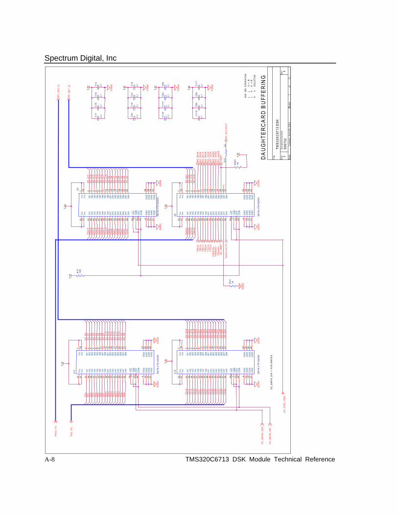
2.6 Daughter Card Interface
The DSK provides three expansion connectors that can be used to accept plug-indaughter cards. The daughter card allows users to build on their DSK platform toextend its capabilities and provide customer and application specific I/O. Theexpansion connectors are for memory, peripherals, and the Host Port Interface (HPI)
The memory connector provides access to the DSP’s asynchronous EMIF signals tointerface with memories and memory mapped devices. It supports byte addressing on32 bit boundries. The peripheral connector brings out the DSP’s peripheral signals likeMcBSPs, timers, and clocks. Both connectors provide power and ground to thedaughter card
The HPI is a high speed interface that can be used to allow multiple DSPs tocommunicate and cooperate on a given task. The HPI connector brings out the HPIspecific control signals.
Most of the expansion connector signals are buffered so that the daughter card cannotdirectly influence the operation of the DSK board. The use of TI low voltage, 5V tolerantbuffers, and CBT interface devices allows the use of either +5V or +3.3V devices to beused on the daughter card.
Other than the buffering, most daughter card signals are not modified on the board. However, a few daughter card specific control signals like DC_RESET andDC_DET exist and are accessible through the CPLD DC_REG register. The DSKalso multiplexes the McBSP0 and McBSP1 of on-board or external use. This functionis controlled through the CPLD MISC register.
3-1
Chapter 3
Physical Description
This chapter describes the physical layout of the TMS320C6713 DSKand its connectors.
Topic Page
3.1 Board Layout 3-23.2 Connector Index 3-33.3 Expansion Connectors 3-33.3.1 J4, Memory Expansion Connector 3-43.3.2 J3, Peripheral Expansion Connector 3-53.3.3 J1, HPI Expansion Connector 3-63.4 Audio Connectors 3-73.4.1 J301, Microphone Connector 3-73.4.2 J303, Audio Line In Connector 3-73.4.3 J304, Audio Line Out Connector 3-83.4.4 J302, Headphone Connector 3-83.5 Power Connectors 3-93.5.1 J5, +5 Volt Connector 3-93.5.2 J6, Optional Power Connector 3-93.6 Miscellaneous Connectors 3-103.6.1 J201, USB Connector 3-103.6.2 J8, External JTAG Connector 3-103.6.3 JP3, PLD Programming Connector 3-113.7 System LEDs 3-113.8 Reset Switch 3-11
Spectrum Digital, Inc
3-2 TMS320VC6713 DSK Module Technical Reference
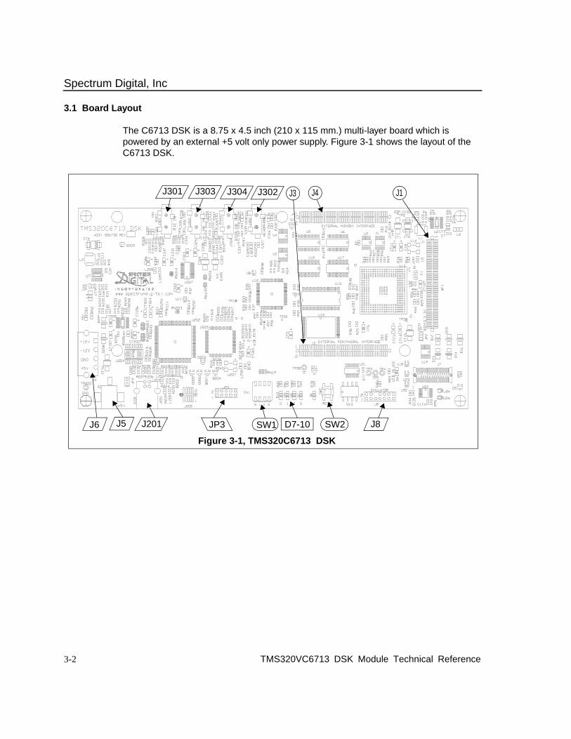
3.1 Board Layout
The C6713 DSK is a 8.75 x 4.5 inch (210 x 115 mm.) multi-layer board which ispowered by an external +5 volt only power supply. Figure 3-1 shows the layout of the C6713 DSK.
Figure 3-1, TMS320C6713 DSK
J4
J5J6 JP3
J302
J8SW1 SW2J201 D7-10
J304J303J301 J3 J1

Spectrum Digital, Inc
3-3
3.2 Connector Index
The TMS320C6713 DSK has many connectors which provide the user accessto the various signals on the DSK.
Note: “*” Not populated
3.3 Expansion Connectors
The TMS320C6713 DSK supports three expansion connectors that follow the TexasInstruments interconnection guidelines. The expansion connector pinouts aredescribed in the following three sections.
The three expansion connectors are all 80 pin 0.050 x 0.050 inches low profileconnectors from Samtec or AMP. The Samtec SFM Series (surface mount) connectorsare designed for high speed interconnections because they have low propagationdelay, capacitance, and cross talk. The connectors present a small foot print on theDSK. Each connector includes multiple ground, +5V, and +3.3V power signals so thatthe daughter card can obtain power directly from the DSK. The peripheral expansionconnector additionally provides both +12V and -12V to the daughter card. Therecommended mating connector, whose part number is TFM-140-32-S-D-LC, is asurface mount connector that provides a 0.465” mated height.
Note: I is on an Input pin O is on an Output pin Z is on a High Impedance pin
Table 1: TMS320C6713 DSK Connectors
Connector # Pins Function
J4 80 Memory
J3 80 Peripheral
J1 80 HPI
J301 3 Microphone
J303 3 Line In
J304 3 Line Out
J303 3 Headphone
J5 2 +5 Volt
J6 * 4 Optional Power Connector
J8 14 External JTAG
J201 5 USB Port
JP3 10 CPLD Programming
SW3 8 DSP Configuration Jumper
Spectrum Digital, Inc
3-4 TMS320VC6713 DSK Module Technical Reference
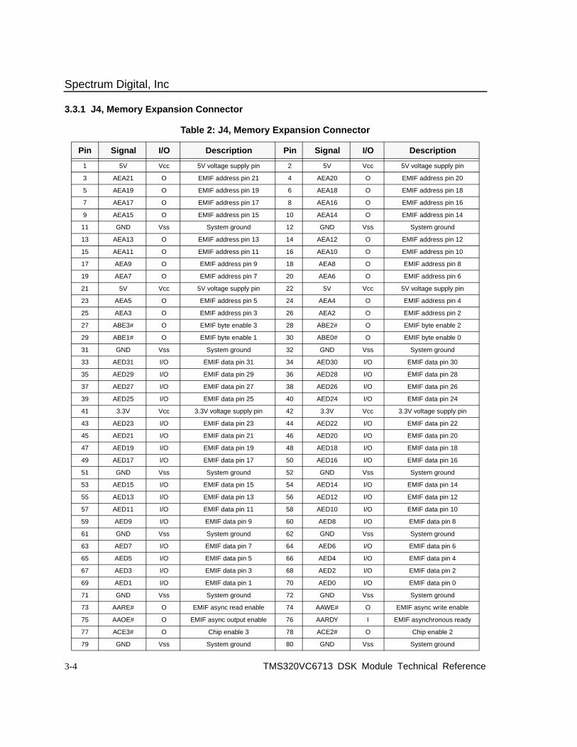
3.3.1 J4, Memory Expansion Connector
Table 2: J4, Memory Expansion Connector
Pin Signal I/O Description Pin Signal I/O Description
1 5V Vcc 5V voltage supply pin 2 5V Vcc 5V voltage supply pin
3 AEA21 O EMIF address pin 21 4 AEA20 O EMIF address pin 20
5 AEA19 O EMIF address pin 19 6 AEA18 O EMIF address pin 18
7 AEA17 O EMIF address pin 17 8 AEA16 O EMIF address pin 16
9 AEA15 O EMIF address pin 15 10 AEA14 O EMIF address pin 14
11 GND Vss System ground 12 GND Vss System ground
13 AEA13 O EMIF address pin 13 14 AEA12 O EMIF address pin 12
15 AEA11 O EMIF address pin 11 16 AEA10 O EMIF address pin 10
17 AEA9 O EMIF address pin 9 18 AEA8 O EMIF address pin 8
19 AEA7 O EMIF address pin 7 20 AEA6 O EMIF address pin 6
21 5V Vcc 5V voltage supply pin 22 5V Vcc 5V voltage supply pin
23 AEA5 O EMIF address pin 5 24 AEA4 O EMIF address pin 4
25 AEA3 O EMIF address pin 3 26 AEA2 O EMIF address pin 2
27 ABE3# O EMIF byte enable 3 28 ABE2# O EMIF byte enable 2
29 ABE1# O EMIF byte enable 1 30 ABE0# O EMIF byte enable 0
31 GND Vss System ground 32 GND Vss System ground
33 AED31 I/O EMIF data pin 31 34 AED30 I/O EMIF data pin 30
35 AED29 I/O EMIF data pin 29 36 AED28 I/O EMIF data pin 28
37 AED27 I/O EMIF data pin 27 38 AED26 I/O EMIF data pin 26
39 AED25 I/O EMIF data pin 25 40 AED24 I/O EMIF data pin 24
41 3.3V Vcc 3.3V voltage supply pin 42 3.3V Vcc 3.3V voltage supply pin
43 AED23 I/O EMIF data pin 23 44 AED22 I/O EMIF data pin 22
45 AED21 I/O EMIF data pin 21 46 AED20 I/O EMIF data pin 20
47 AED19 I/O EMIF data pin 19 48 AED18 I/O EMIF data pin 18
49 AED17 I/O EMIF data pin 17 50 AED16 I/O EMIF data pin 16
51 GND Vss System ground 52 GND Vss System ground
53 AED15 I/O EMIF data pin 15 54 AED14 I/O EMIF data pin 14
55 AED13 I/O EMIF data pin 13 56 AED12 I/O EMIF data pin 12
57 AED11 I/O EMIF data pin 11 58 AED10 I/O EMIF data pin 10
59 AED9 I/O EMIF data pin 9 60 AED8 I/O EMIF data pin 8
61 GND Vss System ground 62 GND Vss System ground
63 AED7 I/O EMIF data pin 7 64 AED6 I/O EMIF data pin 6
65 AED5 I/O EMIF data pin 5 66 AED4 I/O EMIF data pin 4
67 AED3 I/O EMIF data pin 3 68 AED2 I/O EMIF data pin 2
69 AED1 I/O EMIF data pin 1 70 AED0 I/O EMIF data pin 0
71 GND Vss System ground 72 GND Vss System ground
73 AARE# O EMIF async read enable 74 AAWE# O EMIF async write enable
75 AAOE# O EMIF async output enable 76 AARDY I EMIF asynchronous ready
77 ACE3# O Chip enable 3 78 ACE2# O Chip enable 2
79 GND Vss System ground 80 GND Vss System ground
Spectrum Digital, Inc
3-5
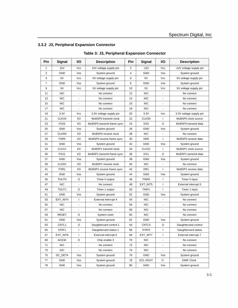
3.3.2 J3, Peripheral Expansion Connector
Table 3: J3, Peripheral Expansion Connector
Pin Signal I/O Description Pin Signal I/O Description
1 12V Vcc 12V voltage supply pin 2 -12V Vcc -12V voltage supply pin
3 GND Vss System ground 4 GND Vss System ground
5 5V Vcc 5V voltage supply pin 6 5V Vcc 5V voltage supply pin
7 GND Vss System ground 8 GND Vss System ground
9 5V Vcc 5V voltage supply pin 10 5V Vcc 5V voltage supply pin
11 N/C - No connect 12 N/C - No connect
13 N/C - No connect 14 N/C - No connect
15 N/C - No connect 16 N/C - No connect
17 N/C - No connect 18 N/C - No connect
19 3.3V Vcc 3.3V voltage supply pin 20 3.3V Vcc 3.3V voltage supply pin
21 CLKX0 I/O McBSP0 transmit clock 22 CLKS0 I McBSP0 clock source
23 FSX0 I/O McBSP0 transmit frame sync 24 DX0 O McBSP0 transmit data
25 GND Vss System ground 26 GND Vss System ground
27 CLKR0 I/O McBSP0 receive clock 28 N/C - No connect
29 FSR0 I/O McBSP0 receive frame sync 30 DR0 I McBSP0 receive data
31 GND Vss System ground 32 GND Vss System ground
33 CLKX1 I/O McBSP1 transmit clock 34 CLKS1 I McBSP1 clock source
35 FSX1 I/O McBSP1 transmit frame sync 36 DX1 O McBSP1 transmit data
37 GND Vss System ground 38 GND Vss System ground
39 CLKR1 I/O McBSP1 receive clock 40 N/C - No connect
41 FSR1 I/O McBSP1 receive frame sync 42 DR1 I McBSP1 receive data
43 GND Vss System ground 44 GND Vss System ground
45 TOUT0 O Timer 0 output 46 TINP0 I Timer 0 input
47 N/C - No connect 48 EXT_INT5 I External interrupt 5
49 TOUT1 O Timer 1 output 50 TINP1 I Timer 1 input
51 GND Vss System ground 52 GND Vss System ground
53 EXT_INT4 I External interrupt 4 54 N/C - No connect
55 N/C - No connect 56 N/C - No connect
57 N/C - No connect 58 N/C - No connect
59 RESET O System reset 60 N/C - No connect
61 GND Vss System ground 62 GND Vss System ground
63 CNTL1 O Daughtercard control 1 64 CNTL0 O Daughtercard control
65 STAT1 I Daughtercard status 1 66 STAT0 I Daughtercard status
67 EXT_INT6 I External interrupt 6 68 EXT_INT7 I External interrupt 7
69 ACE3# O Chip enable 3 70 N/C - No connect
71 N/C - No connect 72 N/C - No connect
73 N/C - No connect 74 N/C - No connect
75 DC_DET# Vss System ground 76 GND Vss System ground
77 GND Vss System ground 78 ECL KOUT O EMIF Clock
79 GND Vss System ground 80 GND Vss System ground

Spectrum Digital, Inc
3-6 TMS320VC6713 DSK Module Technical Reference
3.3.3 J1, HPI Expansion Connector
Table 4: J1, HPI Expansion Connector
Pin Signal I/O Description Pin Signal I/O Description
1 N/C - No connect 2 N/C - No connect
3 GND Vss System ground 4 HPI_RESETn I HPI reset input
5 CLKOUT3 O Clock output3 6 N/C - No connect
7 GND Vss System ground 8 GND Vss System ground
9 HD1/AXR1[7] I/O HPI data 1 10 N/C - No connect
11 HD3/AMUTE1 I/O HPI data 3 12 HD0/AXR1[4] I/O HPI data 0
13 HD5/AHCLKX1 I/O HPI data 5 14 HD2/AFSX1 I/O HPI data 2
15 HD7/GP0[3] I/O HPI data 7 16 HD4/GP0[0] I/O HPI data 4
17 GND Vss System ground 18 HD6/AHCLKR1 I/O HPI data 6
19 HD8/GP0[8] I/O HPI data 8 20 GND Vss System ground
21 HD10/GP0[10] I/O HPI data 10 22 HD9/GP0[9] I/O HPI data 9
23 HD12/GP0[12] I/O HPI data 12 24 HD11/GP0[11] I/O HPI data 11
25 HD14/GP0[14] I/O HPI data 14 26 HD13/GP0[13] I/O HPI data 13
27 GND Vss System ground 28 HD15/GP0[15] I/O HPI data 15
29 HDS2z/AXR1[5] I/O Host data strobe 2 30 GND Vss System ground
31 GND Vss System ground 32 HASz/ACLKX1 I/O Host address strobe
33 HDS1z/AXR1[6] I/O Host data strobe 1 34 GND Vss System ground
35 GND Vss System ground 36 HCNTL0/AXR1[3] I/O Host control 1
37 HCSz/AXR1[2] I/O Host chip select 38 GND Vss System ground
39 GND Vss System ground 40 HHWIL/AFSR1 I/O Host half-word select
41 HCNTL1/AXR1[1] I/O Host control 1 42 GND Vss System ground
43 GND Vss System ground 44 HINTz/GP0[1] I/O Host interrupt
45 HRDYZ/ACLKR1 I/O Host Ready 46 GND Vss System ground
47 GND Vss System ground 48 N/C - No connect
49 HR/Wz/AXR1[0] I/O Host R/W strobe 50 N/C - No connect
51 N/C - No connect 52 N/C - No connect
53 N/C - No connect 54 N/C - No connect
55 N/C - No connect 56 GND Vss System ground
57 N/C - No connect 58 N/C - No connect
59 N/C - No connect 60 N/C - No connect
61 GND Vss System ground 62 N/C - No connect
63 N/C - No connect 64 N/C - No connect
65 N/C - No connect 66 N/C - No connect
67 N/C - No connect 68 SCL0 I/O I2C0 Clock
69 N/C - No connect 70 GND Vss System ground
71 GND Vss System ground 72 SDA0 I/O I2C0 Data
73 N/C - No connect 74 GND Vss System ground
75 GND Vss System ground 76 N/C - No connect
77 N/C - No connect 78 GND Vss System ground
79 GND Vss System ground 80 CLKOUT2/GP0[2] I/O GP I/O 0 bit 2
Spectrum Digital, Inc
3-7
3.4 Audio Connectors
The C6713 DSK has 4 audio connectors. They are described in the followingsections.
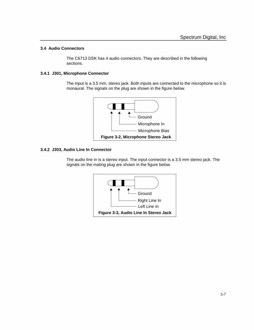
3.4.1 J301, Microphone Connector
The input is a 3.5 mm. stereo jack. Both inputs are connected to the microphone so it ismonaural. The signals on the plug are shown in the figure below.
3.4.2 J303, Audio Line In Connector
The audio line in is a stereo input. The input connector is a 3.5 mm stereo jack. Thesignals on the mating plug are shown in the figure below.
Microphone In
Ground
Figure 3-2, Microphone Stereo Jack
Microphone Bias
Left Line In
Ground
Figure 3-3, Audio Line In Stereo Jack
Right Line In
Spectrum Digital, Inc
3-8 TMS320VC6713 DSK Module Technical Reference
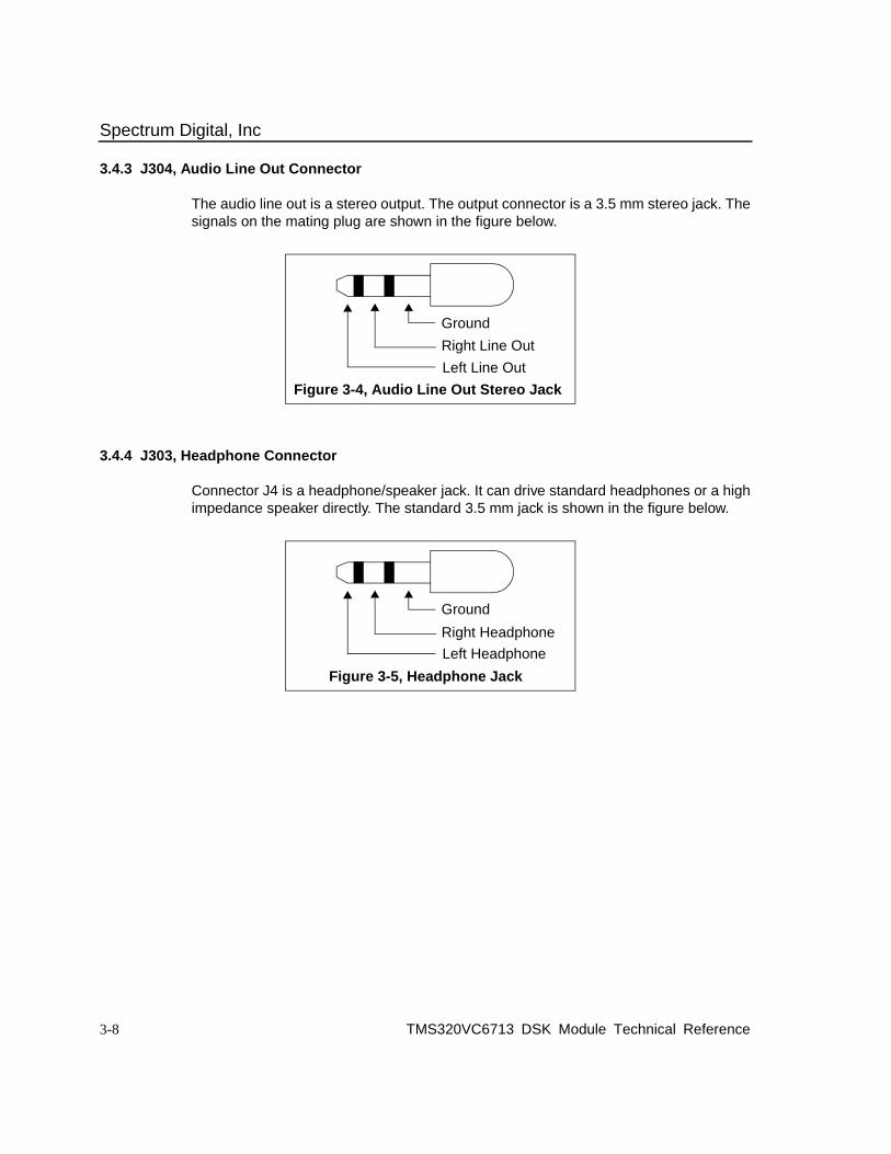
3.4.3 J304, Audio Line Out Connector
The audio line out is a stereo output. The output connector is a 3.5 mm stereo jack. Thesignals on the mating plug are shown in the figure below.
3.4.4 J303, Headphone Connector
Connector J4 is a headphone/speaker jack. It can drive standard headphones or a highimpedance speaker directly. The standard 3.5 mm jack is shown in the figure below.
Left Line Out
Ground
Figure 3-4, Audio Line Out Stereo Jack
Right Line Out
Left Headphone
Ground
Figure 3-5, Headphone Jack
Right Headphone
Spectrum Digital, Inc
3-9
3.5 Power Connectors
The C6713 DSK has 2 power connectors. They are described in the followingsections.
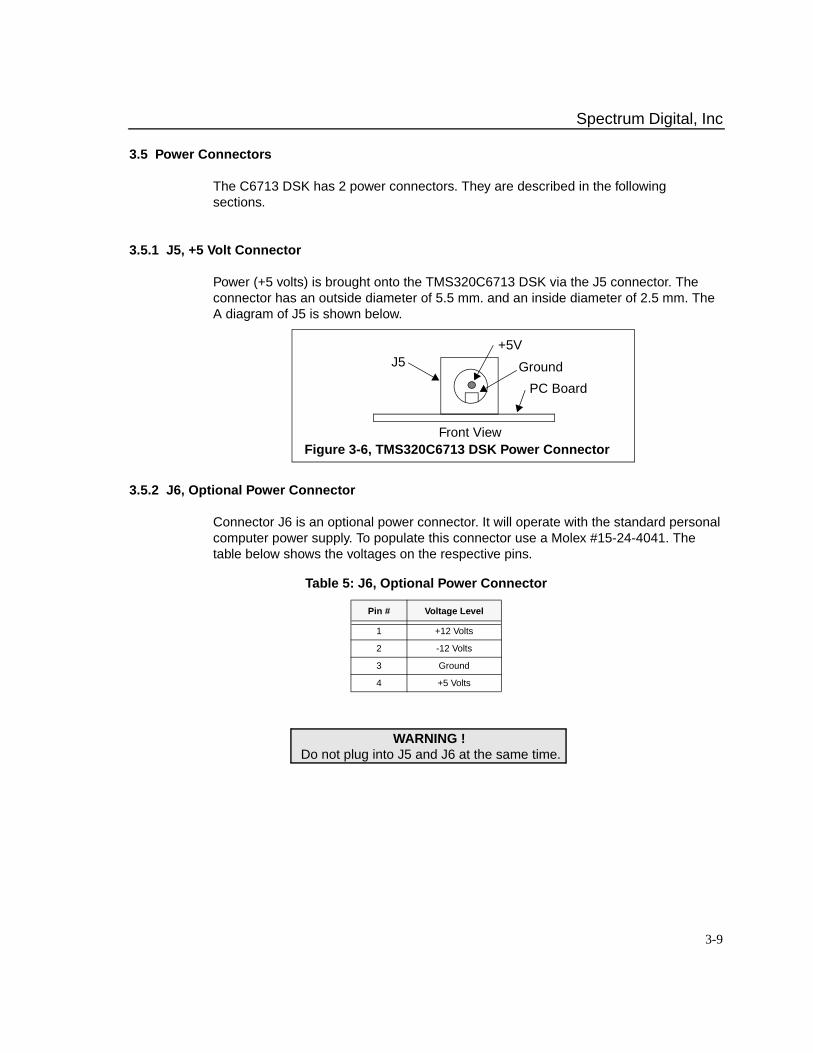
3.5.1 J5, +5 Volt Connector
Power (+5 volts) is brought onto the TMS320C6713 DSK via the J5 connector. Theconnector has an outside diameter of 5.5 mm. and an inside diameter of 2.5 mm. TheA diagram of J5 is shown below.
3.5.2 J6, Optional Power Connector
Connector J6 is an optional power connector. It will operate with the standard personalcomputer power supply. To populate this connector use a Molex #15-24-4041. Thetable below shows the voltages on the respective pins.
Table 5: J6, Optional Power Connector
Pin # Voltage Level
1 +12 Volts
2 -12 Volts
3 Ground
4 +5 Volts
PC Board
J5+5V
Ground
Front ViewFigure 3-6, TMS320C6713 DSK Power Connector
WARNING !Do not plug into J5 and J6 at the same time.
Spectrum Digital, Inc
3-10 TMS320VC6713 DSK Module Technical Reference
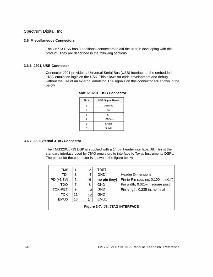
3.6 Miscellaneous Connectors
The C6713 DSK has 3 additional connectors to aid the user in developing with thisproduct. They are described in the following sections.
3.6.1 J201, USB Connector
Connector J201 provides a Universal Serial Bus (USB) Interface to the embeddedJTAG emulation logic on the DSK. This allows for code development and debugwithout the use of an external emulator. The signals on this connector are shown in thebelow.
3.6.2 J8, External JTAG Connector
The TMS320C6713 DSK is supplied with a 14 pin header interface, J8. This is thestandard interface used by JTAG emulators to interface to Texas Instruments DSPs.The pinout for the connector is shown in the figure below.
Table 6: J201, USB Connector
Pin # USB Signal Name
1 USBVdd
2 D+
3 D-
4 USB Vss
5 Shield
6 Shield
1 23 4
5 67 89 1011 1213 14
TMSTDI
PD (+3.3V)TDO
TCK-RET
TCKEMU0
TRST-GNDno pin (key)GNDGND
GNDEMU1
Header Dimensions
Pin-to-Pin spacing, 0.100 in. (X,Y)Pin width, 0.025-in. square post
Pin length, 0.235-in. nominal
Figure 3-7, J8, JTAG INTERFACE

Spectrum Digital, Inc
3-11
3.6.3 JP3, PLD Programming Connector
This connector interfaces to the Altera CPLD, U12. It is used in the in the factory for theprogramming of the CPLD. This connector is not intended to be used outside thefactory.
3.7 System LEDs
TheTMS320C6713 DSK has four system light emitting diodes (LEDs). TheseLEDs indicate various conditions on the DSK. These function of each LED is shown inthe table below.
3.8 Reset Switch
There are three resets on the TMS320C6713 DSK. The first reset is the power onreset. This circuit waits until power is within the specified range before releasing thepower on reset pin to the TMS320C6713.
External sources which control the reset are push button SW2, and the on boardembedded USB JTAG emulator.
Table 7: System LEDs
Reference Designator Color Function On Signal
State
D4 Green USB Emulation in use. When External JTAG Emulator is used this LED is off.
1
D3 Green +5 Volt present 1
D6 Orange RESET Active 1
DS201 Green USB Active, Blinks during USB data transfer 1

Spectrum Digital, Inc
3-12 TMS320VC6713 DSK Module Technical Reference
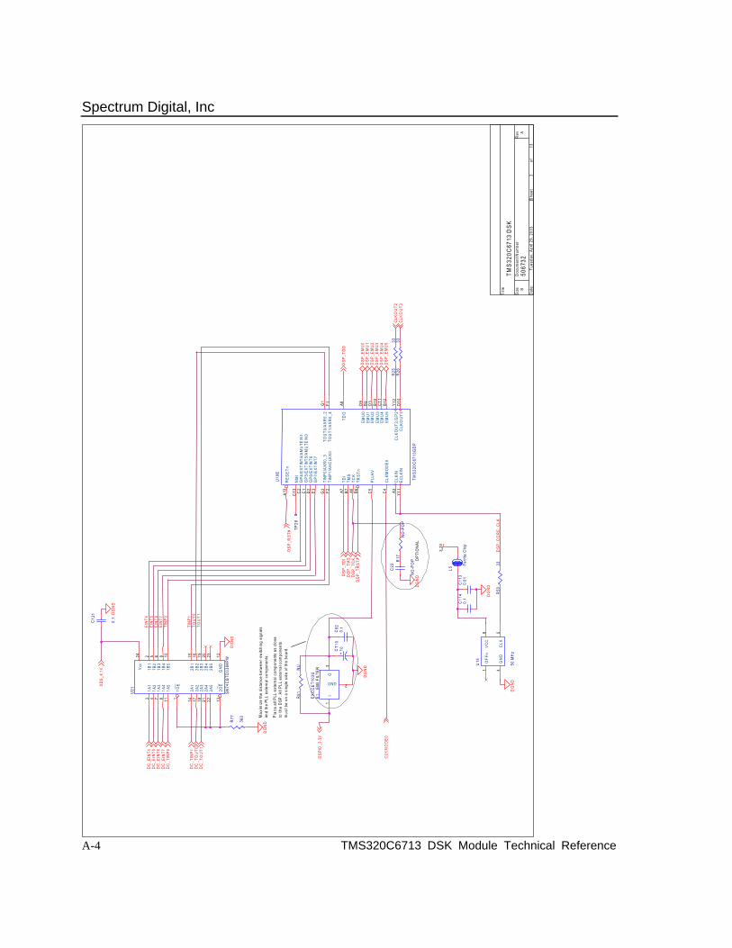
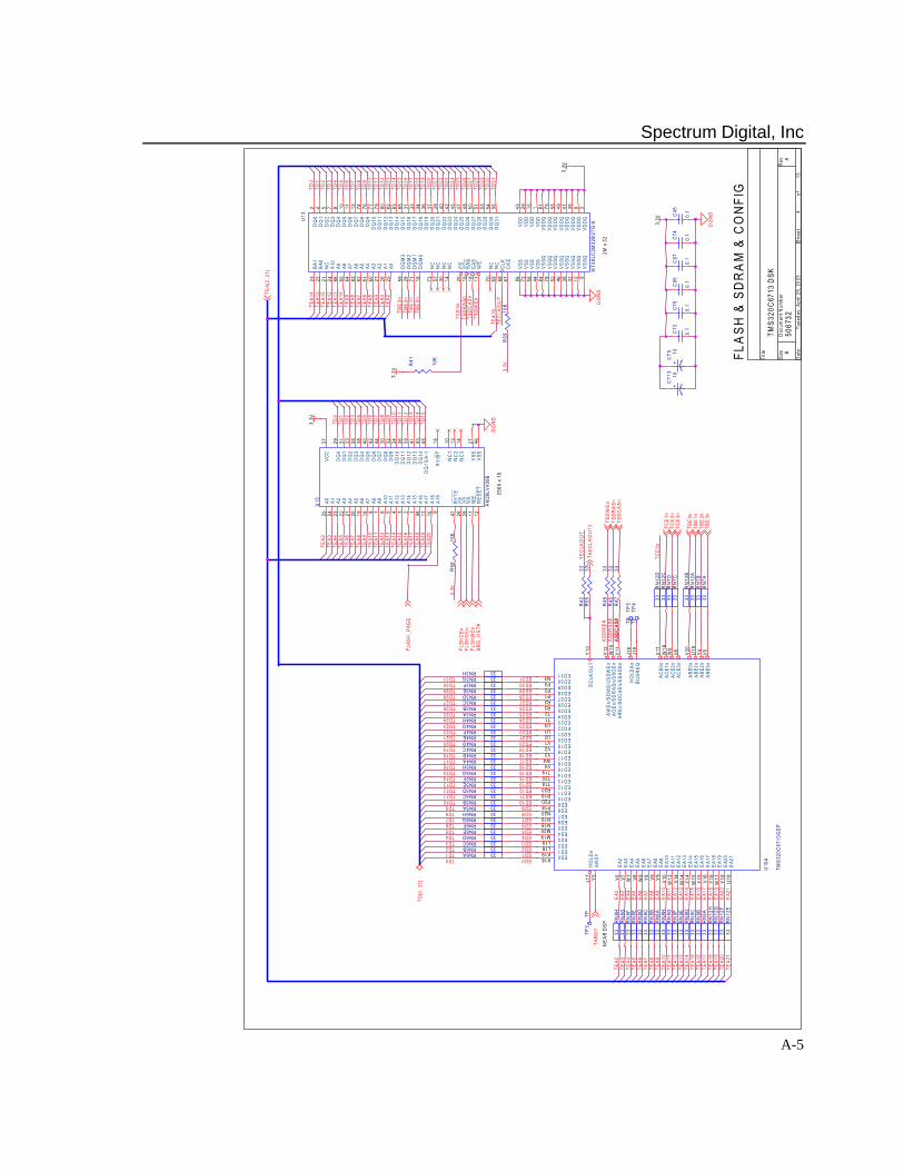
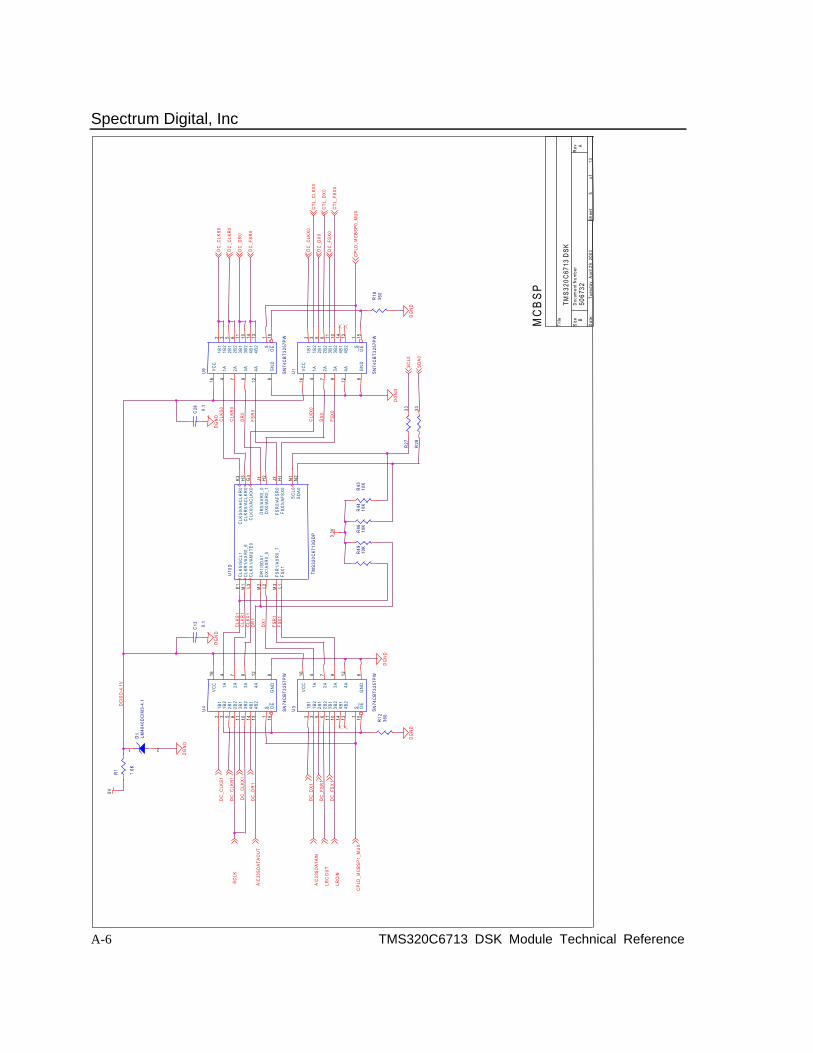
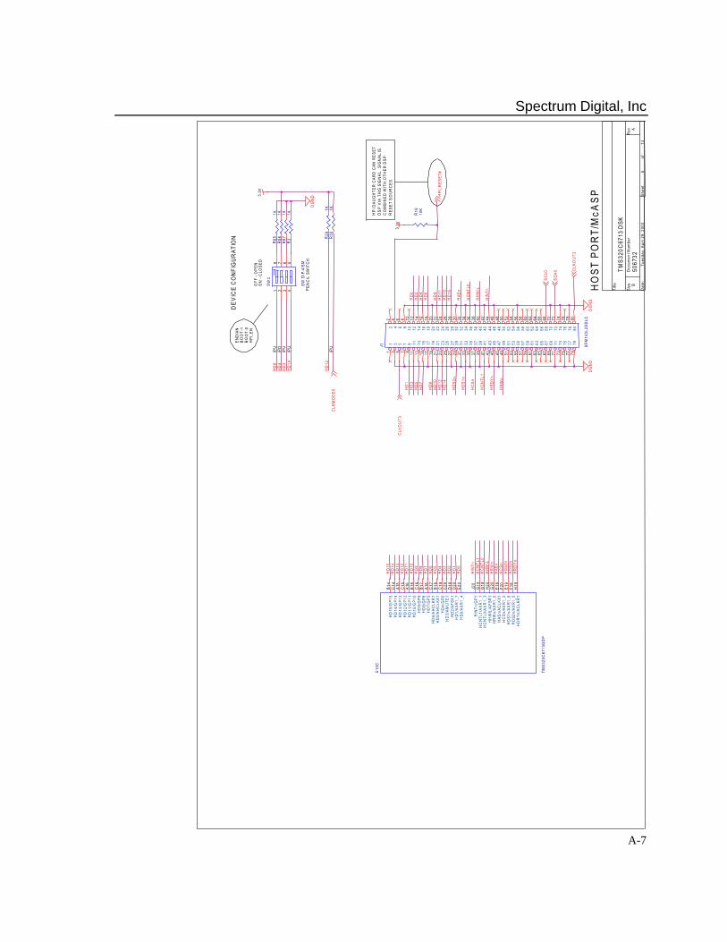
A-1
Appendix A
Schematics
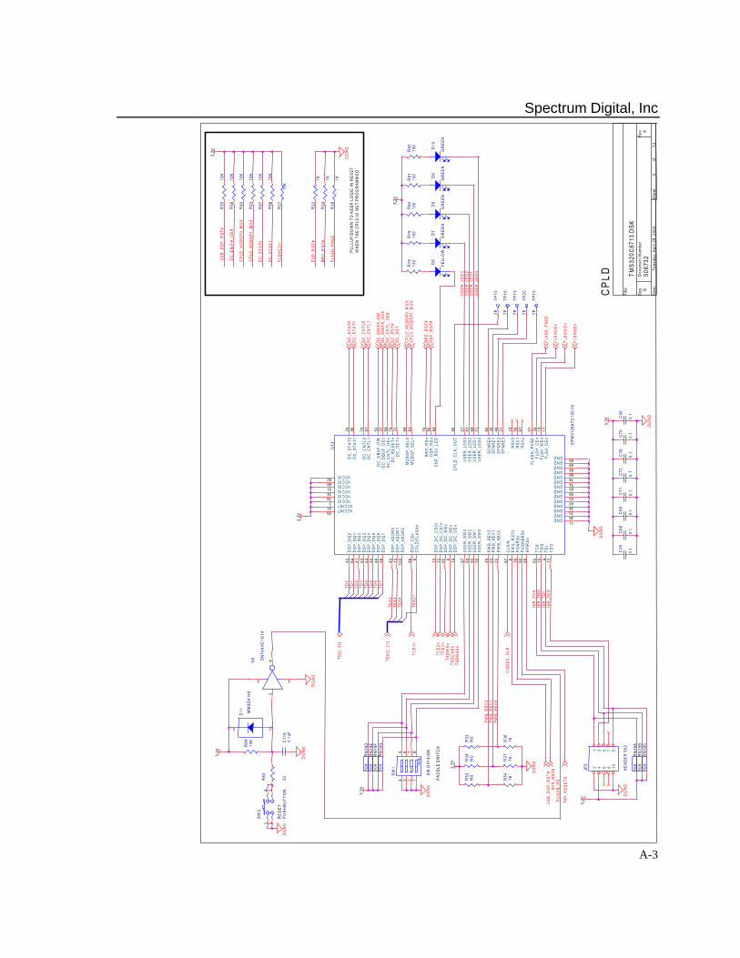
This appendix contains the schematics for the TMS320C6713 DSK.Board components with designators over 200 (e.g. DS201, R211) are partof Spectrum Digital’s embedded JTAG emulator and are not included inthese schematics.
Spectrum Digital, Inc
A-2 TMS320C6713 DSK Module Technical Reference
AA
QA
USED
ON
ENGR
-MGR
RLSE
DATE
DATE
REV
SHDA
TE
DATE
REVI
SION
STA
TUS
OF S
HEET
S
REV
SH
DWN
DATE
ENGR
SH
DATE
CHK
MFG
APPL
ICAT
ION
NEXT
ASS
Y
DATE
REV
23-A
pril-
2003
The
TMS3
20C
6713
DSK
des
ign
is b
ased
on
TMS3
20C
6713
dev
ice
devi
ce d
ata
shee
tSP
RS1
86B
and
erra
ta S
PRZ1
73E.
Thi
ssc
hem
atic
is s
ubje
ct to
cha
nge
with
out n
otific
atio
n. S
pect
rum
Dig
ital I
nc. a
ssum
es n
o lia
bility
for
appl
icat
ions
ass
ista
nce,
cus
tom
er p
rodu
ct d
esig
nor
infri
ngem
ent o
f pat
ents
des
crib
ed h
erei
n.
SPEC
TRU
M D
IGIT
AL IN
CO
RPO
RAT
ED
12
34
56
7
89
1011
1213
14
BA
AA
AA
B
AB
AA
AA
A
REVI
SION
S
DESC
RIPT
ION
REV
DATE
APPR
OVED
ABE
TA23
-Jan
-200
3
5067
32B
TMS3
20C6
713
DSK
B
113
Tues
day,
Apr
il 29
, 200
3
Title
Size
Doc
umen
t Num
ber
Rev
Dat
e:Sh
eet
of
Spectrum Digital, Inc
A-3
CPL
D
P ULL
UP/
DO
WN
TO
KEE
P LO
GIC
IN R
ESET
WH
EN T
HE
CPL
D IS
NO
T PR
OG
RAM
MED
.
RES
ET
PAD
DLE
SW
ITC
H
5067
32A
TMS3
20C6
713
DSK
B
213
Tues
day,
Apr
il 29
, 200
3
Title
Size
Doc
umen
t Num
ber
Rev
Dat
e:Sh
eet
of
USB
_DSP
_RST
#
DSP
_RST
#
DC
_EM
IFA_
OE#
B RD
_RST
#
USE
R_L
ED1
USE
R_L
ED0
USE
R_L
ED3
USE
R_L
ED2
PWB_
REV
2PW
B_R
EV1
PWB_
REV
0
ISR
_TC
KIS
R_T
MS
ISR
_TD
IIS
R_T
DO
PUSH
B_R
S
T EA2
T EA4
T EA3
T D7
TD6
T D5
T D4
T D3
TD2
T D1
TD0
CPL
D_M
CBSP
0_M
UX
CP L
D_M
CBSP
1_M
UX
DC
_STA
T0
DC
_STA
T1
TEA2
1
F LAS
H_P
AGE
F LSH
CEn
SVS_
RST
#
HPI
_RES
ET#
USB
_DSP
_RST
#
TD[0
..31]
TCE
3n
TSD
CAS
nT S
DR
ASn
TCE
2n
T SD
WEn
T EA[
2..2
1]
TCE
1n
DC
_STA
T0D
C_S
TAT1
DC
_CN
TL0
DC
_CN
TL1
DC
_EM
IFA_
OE#
DC_
EMIF
A_DI
R
DC
_CN
TL_O
E#D
C_R
ST#
DC
_DET
CPL
D_M
CBSP
1_M
UX
CPL
D_M
CBSP
0_M
UX
B RD
_RST
#D
SP_R
ST#
CO
DEC
_CLK
FLSH
CEn
F LSH
WEn
FLSH
OEn
FLAS
H_P
AGE
3 .3V
DG
ND
3 .3V
DG
ND
3.3V
DG
ND
3.3V
3.3V
DG
ND
DG
ND
3.3V
DG
ND
DG
ND
3 .3V
DG
ND
3.3V
DG
ND
C68
0.1
C69
0.1
C70
0.1
C39
0.1
C40
0.1
C38
0.1
C71
0.1
C72
0.1
D11 M
MBD
4148
13R
561 0
K
R22
1K
R35
10K
R24
1 K
TP16
TP
TP19
TP
TP20
TP
R79
150
R82
150
R81
150
R80
150
U12 EP
M31
28AT
C10
0-10
4 2 6 4 4 1 6 3 44 4 5 46 5 8 4 0 1 3 1 00 9 8 8
8 51 0 1 2 9 0 9 14 3 5939 497
7 1684 767
2 0232 9
2 5 9 6 7 5 81 52 3 7 54 7 9 3 1 69 8 3 7 6 8 4 80
87 6 3 6 92 99
39913
3451
82
11263338435359
747886
6 0 30 4 8 21
888995
6 2 15 4 73
18
6566
16 5 6 61 3 2 19 1757
DSP
_DQ
0D
SP_D
Q1
DSP
_DQ
2D
SP_D
Q3
DSP
_DQ
4D
SP_D
Q5
DSP
_DQ
6D
SP_D
Q7
DSP
_AD
DR
0D
SP_A
DD
R1
DSP
_AD
DR
2
DSP
_CSn
CPL
D/F
LASH
n
DSP
_RSn
DSP
_DC
_CS0
nD
SP_D
C_C
S1n
DSP
_DC
_WEn
DSP
_DC
_REn
DSP
_DC
_OEn
USE
R_S
W0
USE
R_S
W1
USE
R_S
W2
USE
R_S
W3
USE
R_L
ED0
USE
R_L
ED1
USE
R_L
ED2
USE
R_L
ED3
PWB_
REV0
PWB_
REV1
PWB_
REV2
DC
_STA
T0D
C_S
TAT1
DC
_CN
TL0
DC
_CN
TL1
DC
_DBU
F_D
IRD
C_D
BUF_
OEn
DC
_CN
TL_O
EnD
C_R
ESET
nD
C_D
ETn
MC
BSP_
SEL0
MC
BSP_
SEL1
B RD
_RSn
DSP
_RSn
_LED
CPL
D_C
LK_O
UT
CLK
INEM
U_R
STn
PON
RSn
P USH
BRSn
HPI
RSn
VCCINTVCCINT
VCCIO
VCCIOVCCIO
VCCIO
GNDGNDGNDGNDGNDGNDGND
GNDGNDGND
SPAR
E0SP
ARE1
SPAR
E2SP
ARE3
GNDGNDGND
TCK
T MS
TDI
TDO
VCCIO
GNDVCCIO
RSV
0R
SV1
RSV
2
FLSH
_CEn
F LSH
_WEn
FLSH
_OEn
FLAS
H_P
AGE
R37
1 KR
361 KR
33N
UR
53N
UR
34N
U
R54
1 K
JP3
HEA
DER
5X21
23
45
67
89
10
RN
19A
10K
RN
19C
10K
RN
19B
10K
D6
YELL
OW
D7
GR
EEN
D8
GR
EEN
D9
GR
EEN
D10
GR
EEN
U8 SN
74AH
C1G
14
34
52
R83
33C
1 19
0.1u
F
SW2
PUS
HBU
TTO
N
1 234
R84
10K
R2 3
10K
R40
1 0K
RN
19D
1 0K
RN
19E
1 0K
RN
19F
10K
RN
19G
1 0K
S W1
SW D
IP-4
/SM
1234
8765
R78
150
R57
10K
R39
1K
TP10
TP
R9 8
10K
R97
10K
TP15
TP
Spectrum Digital, Inc
A-4 TMS320C6713 DSK Module Technical Reference
Pla
c e a
ll PL
L ex
tern
al c
ompo
nent
s as
clo
seto
the
DSP
. All
PLL
exte
rnal
com
pone
nts
mus
t be
on a
sin
gle
side
of t
he b
oard
.
Max
i miz
e th
e di
stan
ce b
etw
een
switc
hing
sig
nals
a n
d th
e PL
L ex
tern
al c
ompo
nent
s.
OPT
ION
AL
5067
32A
TMS3
20C6
713
DSK
B
313
Tues
day,
Apr
il 29
, 200
3
Title
Size
Doc
umen
t Num
ber
Rev
Dat
e:Sh
eet
of
DSP
_CO
RE_
CLK
EIN
T4EI
NT5
E IN
T6E I
NT7
TIN
P0
TIN
P1T O
UT0
TOU
T1
DSP
_TD
O
DSP
_TR
ST#
DSP
_TM
SD
SP_T
DI
DSP
_TC
K
DSP
_EM
U0
DSP
_EM
U1
DSP
_RST
#
DC
_EIN
T4
DC
_EIN
T6D
C_E
INT7
DC
_TIN
P0
DC
_TIN
P1
DC
_EIN
T5
DC
_TO
UT0
DC
_TO
UT1
DSP
_EM
U4
DSP
_EM
U5
DSP
_EM
U2
DSP
_EM
U3
XDS_
4.1V
DSP
IO_3
.3V
CLK
MO
DE0
CLK
OU
T2C
LKO
UT3
DG
ND
3.3V
DG
ND
DG
ND
DG
ND
DG
ND
DG
ND
DG
ND
U10
E
TMS3
20C
6713
GD
P
D9
B 9 D3
B 10
C11
B12
A8G1
F 1
A 3C4
C5
A13
C13 E 3D
2C
1C
2
G2 F 2 A7 B 7 A6 B 6 Y11
D10
Y 12
E MU
0EM
U1
EMU
2EM
U3
EMU
4EM
U5
TDO
TOU
T0/A
XR0_
2T O
UT1
/AXR
0_4
CLK
IN
CLK
MO
DE0
PLLH
V
RES
ETn
NM
I
GP7
/EXT
INT7
GP6
/EXT
INT6
GP5
/EXT
INT5
/AM
UTE
IN0
GP4
/EXT
INT4
/AM
UTE
IN1
TINP
0/AX
R0_3
T IN
P1/A
HC
LKX0
TDI
T MS
TCK
T RST
n
E CLK
INC
LKO
UT3
CLK
OU
T2/G
P2
C92
0 .1
TP28
E1E XC
CET
103U
EMI F
ILTE
R
13
2
IO
GND
+C
T10
1 0
C1 2
1
0 .1
C11
30.
01
R77
3 60
C22
NO
-PO
P
C11
40.
1
R17
NO
-PO
P
U14
50 M
Hz
1 4
8 5
OFF
n
GN
D
VCC
CLK
L5
Ferri
te C
hip
R50
33
R25
33R
2633
U2 1
SN74
CBT
D33
84PW
1 133 4 7 8 11
2 5 6 9 10
1 4 17 1 8 21 22
24 121 5 16 1 9 20 23
1OE
2OE
1A1
1 A2
1 A3
1A4
1A5
1B1
1 B2
1 B3
1B4
1B5
2A1
2 A2
2A3
2A4
2A5
V cc
GN
D
2B1
2 B2
2B3
2B4
2B5
R51
NU
Spectrum Digital, Inc
A-5
FLA
SH &
SD
RA
M &
CO
NFI
G
NEA
R D
SP
2 56K
x 1
6
2M x
32
5067
32A
TMS3
20C6
713
DSK
B
413
Tues
day,
Apr
il 29
, 200
3
Title
Size
Doc
umen
t Num
ber
Rev
Dat
e:Sh
eet
of
T EA1
1
T D23
T D22
TEA1
5
TEA5
TEA1
2
T D26
TD21
T D20
TD11
TD9
TD7
T D4
T BE
2n
T EA3
T D31
T D28
TD27
TEA4
T D29
T D18
TD3
TEA8
TD13
T D5
T BE
3n
T BE
1n
T D24
TD1
TD19
TD2
T D15
T D8
TD17
TD25
TD10
TEA1
3T E
A14
T EA7
T EA1
0
T D30
T D16
TEA6
T BE
0n
TD6
TEA9
T D12
TEA2
T D14
T D0
T SD
RAS
nTS
DC
ASn
T SD
WEn
TCE
0n
T EC
LKO
UT
3.3V
T EA1
6
T D11
TD9
TD7
T D4
TD3
TD13
TD5
T D1
TD2
TD15
T D8
T D10
TD6
T D12
T D14
T D0
TEA2
TEA3
T EA4
T EA5
TEA6
TEA7
T EA8
TEA9
TEA1
0TE
A11
T EA1
2TE
A13
T EA1
4T E
A15
T EA1
6TE
A17
T EA1
8
T EA2
0TE
A19
EA21
EA20
EA19
EA18
EA17
EA16
EA15
EA14
EA13
EA12
EA11
EA10
EA9
EA8
EA7
EA6
EA5
EA4
E A3
EA2
ED0ED1ED2ED3ED4ED5ED6ED7ED8ED9ED10ED11ED12ED13ED14ED15ED16ED17ED18ED19ED20ED21ED22ED23ED24ED25ED26ED27ED28ED29ED30ED31
TEA2
1TE
A20
TEA1
9TE
A18
TEA1
7TE
A16
TEA1
5TE
A14
TEA1
3TE
A12
TEA1
1TE
A10
TEA9
TEA8
TEA7
TEA6
TEA5
TEA4
T EA3
TEA2
TD0TD1TD2TD3TD4TD5TD6TD7TD8TD9TD10
TD19
TD17
TD14
TD16
TD12
TD18
TD13
TD11
TD15
TD25
TD22
TD29
TD23
TD20
TD24
TD21
TD28TD27TD26
TD31TD30
TCE
0n
ASDW
E#AS
DR
AS#
ASD
CAS
#AS
DC
AS#
TEC
LKO
UT
3 .3V
BRD
_RST
#
F LSH
CEn
FLSH
OEn
F LSH
WEn
T AEC
LKO
UT2 TC
E1n
T CE
2nTC
E3n
T BE
0nTB
E1n
TBE
2nTB
E3n
TSD
WEn
T SD
RAS
nTS
DC
ASn
TAR
DY
T D[0
..31]
TEA[
2..2
1]
F LAS
H_P
AGE
3 .3V
3.3V
DG
ND
DG
ND
3 .3V
3 .3V
DG
ND
RN8
A33
R41
10K
RN
12F
33
RN
8B33
RN
12G
33
RN
8C33
RN
12H
33
RN
8D33
RN9
A33
RN
7B33
RN7
A33
RN
12B
33R
N12
A33
RN
8E33
C97
0.1
RN
9B33
C75
0.1
C73
0.1
RN6F 33
RN6H 33
RN4B 33
RN5F 33RN5E 33RN5D 33
RN5B 33
C95
0.1
RN3C 33
RN3A 33
RN3G 33
RN5C 33
RN4D 33
RN6A 33
RN3D 33
RN6C 33
RN
8F33
RN6G 33
RN4A 33RN5H 33
RN6E 33
RN3E 33
RN6D 33
RN4G 33
RN4C 33
RN4F 33
RN3F 33
RN4H 33
RN4E 33
RN5G 33
RN6B 33
RN3H 33
RN3B 33
RN5A 33
RN
9C33
C74
0.1
C45
0.1
U13
MT4
8LC
2M32
B2T
G-6
2 4 5 7 8 1 0 11 13 74 7 6 77 7 9 80 8 2 83 85 31 3 4 3 6 3 7 3 9 4 0 42 4 5 47 4 8 50 5 1 5 3 5 4 5633
2 4 66 6 5 64 63 62 6 1 60 2 7 26 2 523 22 6 8 672071 1 6 1 9 18 1 759 28 8 6 7 2 5 8 4 4 8 4 7 8 52 4 6 38 3 2 12 6
4 3 2 9 1 5 1 8 1 7 5 55 4 9 41 3 5 9 3
2 1 7 0 697 3 5 7 3 0 14
DQ
0D
Q1
DQ
2D
Q3
DQ
4D
Q5
DQ
6D
Q7
DQ
8D
Q9
DQ
10D
Q11
DQ
12D
Q13
DQ
14D
Q15
DQ
16
DQ
18D
Q19
DQ
20D
Q21
DQ
22D
Q23
DQ
24D
Q25
DQ
26D
Q27
DQ
28D
Q29
DQ
30D
Q31
DQ
17
A 10
A 9 A8 A7 A6 A5 A4 A3 A2 A1 A0BA1
BA0
CLK
CKE
CS
DQ
M1
DQ
M0
RAS
CAS
WE
DQ
M3
DQ
M2
V SS
V SS
VSS
V SS
VSSQ
V SSQ
VSSQ
VSSQ
VSSQ
V SSQ
VSSQ
V SSQ
V DD
V DD
VDD
V DD
VDDQ
V DDQ
VDDQ
VDDQ
VDDQ
V DDQ
VDDQ
V DDQ
NC
NC
NC
NC
NC
NC
NC
RN
8G3 3
RN
9D33
R42
33
RN
8H33
R55
33
RN
9E33
TP5
TPTP
4TP
TP3
TP
RN
9F33
+C
T5 10
R45
3 3
RN
9G33
U10
A
TMS3
20C
6713
GD
P
V5Y4U19
V20
V6W6
W18
V17
J19
J 18
V11
W10
V 12
Y10
K18K19L18L19M19M20N18N19N20P18P20R19R20T18T20T19V4W4Y3V2V1U2U1U3T1T2R3R2P1P2P3N3
U18Y1
8W
17Y16
V16
Y15
W15Y1
4W
14V14
W13V1
0Y9V 9Y8W8V8W7V7Y6Y 5J17
ABE3
nAB
E2n
ABE1
nAB
E0n
ACE3
nAC
E2n
ACE1
nA C
E0n
B USR
EQH
OLD
An
AREn
/SD
CAS
n/SS
ADSn
AOEn
/SD
RAS
n/SS
OEn
AWEn
/SD
WEn
/SSW
En
E CLK
OU
T
ED0ED1ED2ED3ED4ED5ED6ED7ED8ED9
ED10ED11ED12ED13ED14ED15ED16ED17ED18ED19ED20ED21ED22ED23ED24ED25ED26ED27ED28ED29ED30ED31
EA21
EA20
EA19
EA18
EA17
EA16
EA15
EA14
EA13
EA12
EA11
EA10
E A9
EA8
EA7
EA6
E A5
EA4
EA3
EA2
ARDY
HO
LDn
+C
T13
10
R48
33
R47
33R58
1 0K
RN
12D
33
RN
7C33
RN
12C
33R
N7D
33
U15
A M29
LV40
0B
2 1 4 8345678 9
10 1 3 14
1 61 81920212 2232 42 53 7 4 627
26 2 8 11 1 24 7
1 529 3 1 33 35 38 4 0 42 4 4 30 3 2 34 36 39 41 4 3 4 51 7
A 14
A15
A 16
A13
A12
A11
A 10
A9A 8 A19
NC
1N
C2
NC
3
A 18
A 7A6A5A4A3A 2A 1A0VC
C
VSS
V SS
CE
OE
WE
RES
ET
B YTE
RY/
BY
DQ
0D
Q1
DQ
2D
Q3
DQ
4D
Q5
DQ
6D
Q7
DQ
8D
Q9
DQ
10D
Q11
DQ
12D
Q13
DQ
14D
Q15
/A-1
A17
RN
9H33
R59
10K
RN
12E
33
Spectrum Digital, Inc
A-6 TMS320C6713 DSK Module Technical Reference
MC
BSP
5067
32A
TMS3
20C6
713
DSK
B
513
Tues
day,
Apr
il 29
, 200
3
Title
Size
Doc
umen
t Num
ber
Rev
Dat
e:Sh
eet
of
DR
1
DX1
F SX1
F SR
1
CLK
R1
CLK
X1
DCI
SO-4
.1V
CLK
S1
CLK
S0
CLK
R0
DR
0
FSR
0
F SX0
DX0
CLK
X0
DC
_DR
0
DC
_CLK
R0
DC
_CLK
S0
DC
_FSX
0
DC
_CLK
S1
DC
_CLK
R1
DC
_CLK
X1
DC
_DR
1
DC
_FSR
1
DC
_FSX
1
DC
_DX1
A IC
23SD
ATAO
UT
A IC
23SD
ATAI
N
B CLK
L RCI
N
LRC
OU
T
CPL
D_M
CBSP
1_M
UX
CPL
D_M
CBSP
0_M
UX
CTL
_FSX
0
SCL0
SDA0
DC
_CLK
X0C
TL_C
LKX0
DC
_FSR
0
CTL
_DX0
DC
_DX0
DG
ND
DG
ND
5V
DG
ND
DG
ND
DG
ND
DG
ND
DG
ND
3 .3V
R12
3 60
R27
33
R28
33
U9
SN74
CBT
3257
PW
4
1 4
711
9 1 21 3 12 1 5103 5 6
1 6 8
1A
4 B1
2A3 B
13A 4A
4B2 S
1 B1
OE
3B2
1B2
2B1
2B2
VCC
GN
D
R18
3 60
U1 0
D
T MS3
20C
6713
GD
P
K3 H3
G3
J 1 H2
J3 H1
E1 M1 L 3 M2 L 2 M3 L 1
N1
N2
CLK
S0/A
HCLK
R0
CLK
R0/
ACLK
R0
CLK
X0/A
CLK
X0
DR0
/AXR
0_0
DX0
/AXR
0_1
FSR
0/AF
SR0
F SX0
/AFS
X0
CLK
S/SC
L1C
LKR
1/AX
R0_6
CLK
X1/A
MU
TE0
DR
1/SD
A1D
X1AX
R0_
5
FSR1
/AXR
0_7
F SX1
S CL0
S DA0
R1
1 .6K
D1 LM
4040
DCI
M3-
4.1
21
C28 0 .
1
C13 0 .
1
R49
10K
R46
10K
R44
10K
R43
10K
U4
SN74
CBT
3257
PW
4
1 4
711
9 1 21 3 12 1 5103 5 6
1 6 8
1A
4 B1
2A3 B
13A 4A
4B2
S1 B1
OE
3B2
1B2
2B1
2B2
VCC
GN
D
U1
S N74
CBT
3257
PW
4
1 4
711
9 1 21 3 12 1 51 03 5 6
1 6 8
1 A
4 B1
2 A3 B
13 A 4 A
4 B2 S
1B1
OE
3 B2
1 B2
2 B1
2 B2
VCC
GN
D
U3
S N74
CBT
3257
PW
4
1 4
711
9 1 21 3 12 1 51 03 5 6
1 6 8
1 A
4 B1
2 A3 B
13 A 4 A
4 B2
S1B1
OE
3 B2
1 B2
2 B1
2 B2
VCC
GN
D
Spectrum Digital, Inc
A-7
HO
ST P
OR
T/M
cASP
HPI
DAU
GH
TER
CAR
D C
AN R
ESET
DS
P VI
A T
HIS
SIG
NAL
. SI
GN
AL IS
CO
MBI
NED
WIT
H O
THER
DSP
RES
ET S
OU
RC
ES.
P EN
CIL
SW
ITC
H
E ND
IAN
BOO
T-1
BOO
T-0
OFF
- O
PEN
ON
- C
LOSE
D
i PU
iPU
i PU
iPD
iPU
HPI
_EN
DEV
ICE
CO
NFIG
URAT
ION
5067
32A
TMS3
20C6
713
DSK
B
613
Tues
day,
Apr
il 29
, 200
3
Title
Size
Doc
umen
t Num
ber
Rev
Dat
e:Sh
eet
of
HD
1H
D3
HD
5H
D7
HD
12H
D14
HD
S2n
HD
S1n
HC
NTL
1
HR
DYn
HR
Wn
HC
Sn
HD
0H
D2
HD
4H
D6
HD
9H
D11
HD
13H
D15
HAS
n
HC
NTL
0
HHW
IL
HIN
Tn
HD
10H
D8
HD
8H
D4
HD
3H
D14
HD
12
HD
15H
D14
HD
13H
D12
HD
11H
D10
HD
9H
D8
HD
7H
D6
HD
5H
D4
HD
3H
D2
HD
1H
D0
HIN
TnH
CN
TL1
HC
NTL
0H
HWIL
HR
Wn
HAS
nH
CSn
HD
S1n
HR
DYn
HD
S2n
HPI
_RES
ET#
CLK
MO
DE0
CLK
OU
T2
CLK
OU
T3
SCL0
S DA0
3 .3V
DG
ND
DG
ND
DG
ND3.
3V
R19
10K
R29
1 KR
301K
J 1 SFM
140L
2SD
LC
12
34
56
78
910
1 11 2
1 31 4
1 51 6
1 71 8
1 92 0
2 12 2
2 32 4
2526
2 72 8
2930
3 13 2
3334
3 53 6
3738
3 94 0
4142
4 34 4
4546
4748
4950
5 15 2
5354
5556
5758
5 96 0
6162
6364
6566
6768
6970
7172
7374
7576
7778
7980
12
34
56
78
91 0
1 11 2
1 31 4
1 51 6
1718
1 92 0
2122
2 32 4
2526
2728
2930
3 13 2
3334
3 53 6
3 73 8
3940
4142
4344
4546
4748
4950
5152
5 35 4
5556
5758
5960
6 16 2
6364
6566
6768
6970
7172
7374
7576
7778
7980
S W3
SW D
IP-4
/SM
1 2 3 4
8 7 6 5R
871K
R85
1 KR
8 61K
R3
1 K
U10
C
TMS3
20C
6713
GD
P
B 14
C14
A15
C15
A16
B 16
C16
B 17
A 18
C17
B 18
C19
C20
D18
D20
E 20
H19
F18
E 19
F20
E18
G20
H20
G18
G19
J20
HD
15/G
P15
HD
14/G
P14
HD
13/G
P13
HD
12/G
P12
HD
11/G
P11
HD
10/G
P10
HD
9/G
P9H
D8/
GP8
HD
7/G
P3H
D6/
AHC
LKR
1H
D5/
AHC
LKX1
HD
4/G
P0H
D3/
AMU
TE1
HD2
/AFS
X1H
D1/A
XR1_
7H
D0/A
XR1_
4
HD
RYn
/AC
LKR
1H
DS2
n/AX
R1_5
HD
S1n/
AXR1
_6H
CSn
/AXR
1_2
HAS
n/AC
LKX1
HR
Wn/
AXR1
_0H
HW
IL/A
FSR
1H
CN
TL0/
AXR
1_3
HC
NTL
1/AX
R1_
1H
INTn
/GP1
Spectrum Digital, Inc
A-8 TMS320C6713 DSK Module Technical Reference
#OE
DIR
OPE
RAT
ION
L
L
A <-
- BL
H
A
--> B
H
X
ISO
LATI
ON
DA
UG
HTE
RC
AR
D B
UFF
ERIN
GD
C_E
MIF
A_D
IR =
1 FO
R W
RITE
S
5067
32B
TMS3
20C6
713
DSK
B
713
Tues
day,
Apr
il 29
, 200
3
Title
Size
Doc
umen
t Num
ber
Rev
Dat
e:Sh
eet
of
TEA1
2
DC
_D30
DC
_D16
DC
_D26
DC
_D14
DC
_D15
DC
_D4
T EA8
DC
_D10
DC
_D21
DC
_D25
T D17
DC
_A19
TEA3
T D11
T D1
DC_
A2T E
A2
T EA2
0
TEA1
1
TD21
DC
_A16
DC
_D19
DC
_D23
DC
_D3
DC
_A11
DC
_A20
TEA1
3
DC
_D24
DC
_D22
DC
_D8
DC_
A8D
C_A9
T EA2
1
DC
_D11
DC
_D17
TEA9
TD18
T D13
DC
_D6
DC
_D1
DC_
A7
DC
_D20
DC_
A6
TEA1
9
TEA5
DC
_D5
DC
_D0
DC
_A15
T EA7
T D9
T D15
T EA1
4
DC
_D12
DC
_D31
T EA1
0D
C_D
7
DC
_D28
T EA6
DC
_D9
TD24
DC
_D2
DC_
A4
TEA1
6
T D16
DC
_A14
DC
_A21
DC_
A3
TEA1
8
T D0
DC
_D18
DC
_D27
T EA1
7
DC
_A18
DC_
A5
DC
_A10
DC
_A17
T EA4
TEA1
5
TD8
DC
_D13
T D31
DC
_D29
TD2
TD3
T D4
TD5
TD6
TD7
TD14
T D12
TD10 TD
19TD
20
TD22
TD23
TD30
T D29
TD28
TD27
TD26
TD25
DC
_A12
DC
_A13
DC
_A[2
1..2
]
TEA[
2..2
1]
T D[0
..31]
DC
_D[3
1..0
]
TSD
WEn
TSD
CAS
n
T AEC
LKO
UT2
TBE
0n
TBE
2n
T CE
3n
TSD
RAS
n
DC
_AR
DY
TCE
2n
T BE
3n
T BE
1nD
C_B
E2#
TAR
DY
DC
_EC
LKO
UT
DC
_BE3
#
DC
_BE0
#D
C_C
E3#
DC
_AW
E#D
C_A
OE#
DC
_AR
E#
DC
_BE1
#
DC
_CE2
#
DC
_CN
TL_O
E#
DC_
EMIF
A_DI
R
DC
_EM
IFA_
OE#
DG
ND
3.3V
DG
ND
3 .3V
DG
ND
3.3V
3 .3V
3 .3V
3 .3V 3 .
3V
DG
ND
DG
ND
DG
ND
DG
ND
DG
ND
DG
ND
DG
ND
DG
ND
DG
ND
3 .3V
DG
ND
3 .3V
3.3V
U16
SN74
LVTH
1624
5A
7 18314 2 47 4 6 44 4 3 41 4 0 38 3 7
2 3 5 6 8 9 11 1 236 35 33 3 2 30 29 27 2 6
13 14 16 1 7 19 20 22 2 3
48 1 25 24 4 10 15 21
28 34 39 45
V cc
Vcc
Vcc
V cc
1A1
1 A2
1A3
1 A4
1 A5
1A6
1A7
1A8
1B1
1 B2
1B3
1 B4
1 B5
1B6
1B7
1B8
2A1
2A2
2A3
2A4
2 A5
2A6
2A7
2A8
2B1
2B2
2B3
2B4
2 B5
2B6
2B7
2B8
1OE
1DIR
2OE
2DIR
GN
DG
ND
GN
DG
ND
GN
DG
ND
GN
DG
ND
R40
31K
U6
SN74
LVTH
1624
5A
7 18314 2 47 4 6 44 4 3 41 4 0 38 3 7
2 3 5 6 8 9 11 1 236 35 33 3 2 30 29 27 2 6
13 14 16 1 7 19 20 22 2 3
48 1 25 24 4 10 15 21
28 34 39 45
V cc
Vcc
Vcc
V cc
1A1
1 A2
1A3
1 A4
1 A5
1A6
1A7
1A8
1B1
1 B2
1B3
1 B4
1 B5
1B6
1B7
1B8
2A1
2A2
2A3
2A4
2 A5
2A6
2A7
2A8
2B1
2B2
2B3
2B4
2 B5
2B6
2B7
2B8
1OE
1DIR
2OE
2DIR
GN
DG
ND
GN
DG
ND
GN
DG
ND
GN
DG
ND
R15
33
C15
0.1
C17
0.1
C16
0.1
C14
0.1
U17
S N74
LVTH
1624
5A
7 1 83 142 47 4 6 44 43 41 4 0 38 3 7
2 3 5 6 8 9 11 1 236 3 5 33 32 30 29 2 7 2 6
13 1 4 16 17 19 20 2 2 2 3
4 8 1 25 2 4 4 10 1 5 2 1
2 8 34 3 9 4 5
V cc
Vcc
Vcc
V cc
1 A1
1A2
1A3
1A4
1A5
1 A6
1 A7
1A8
1 B1
1B2
1B3
1B4
1B5
1 B6
1 B7
1B8
2 A1
2A2
2A3
2A4
2 A5
2A6
2 A7
2A8
2 B1
2B2
2B3
2B4
2 B5
2B6
2 B7
2B8
1OE
1 DIR
2OE
2 DIR
GN
DG
ND
GN
DG
ND
GN
DG
ND
GN
DG
ND
R14
1K
C20
0 .1
R13
10K
C19
0 .1
C21
0 .1
C18
0 .1
U5
S N74
LVTH
1624
5A
7 1 83 14 2 4 7 46 44 43 4 1 40 3 8 37
2 3 5 6 8 9 1 1 123 6 35 33 32 30 2 9 2 7 2 6
1 3 14 16 17 19 2 0 2 2 2 3
4 8 1 2 5 24 4 1 0 1 5 2 1
28 3 4 3 9 4 5
Vcc
V cc
V cc
Vcc
1A1
1A2
1A3
1A4
1 A5
1 A6
1A7
1 A8
1B1
1B2
1B3
1B4
1 B5
1 B6
1B7
1 B8
2A1
2A2
2A3
2 A4
2A5
2 A6
2A7
2 A8
2B1
2B2
2B3
2 B4
2B5
2 B6
2B7
2 B8
1 OE
1DIR
2 OE
2DIR
GN
DG
ND
GN
DG
ND
GN
DG
ND
GN
DG
ND
C96
0 .1
C94
0 .1
C11
5
0 .1
C11
6
0 .1
C11
7
0.1
C99
0.1
C98
0.1
C11
8
0.1
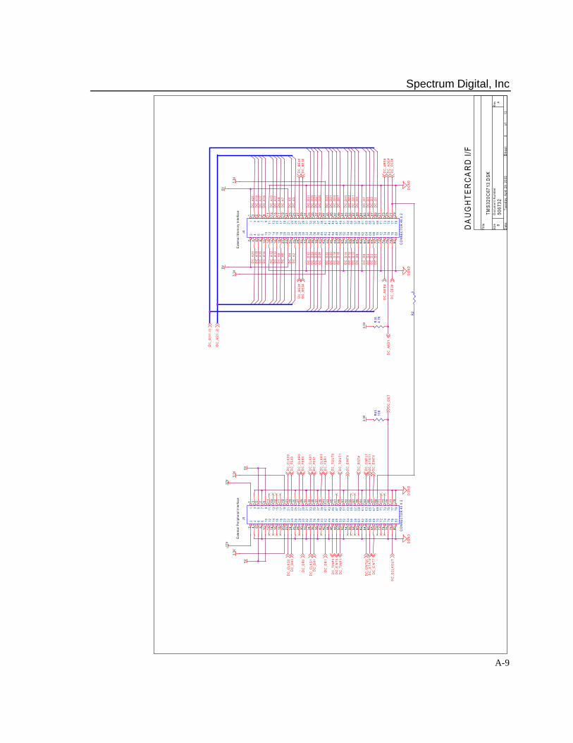
Spectrum Digital, Inc
A-9
DA
UG
HTE
RCA
RD
I/F
Exte
rnal
Mem
ory
Inte
rface
Exte
rnal
Per
iphe
ral I
nter
face
5067
32A
TMS3
20C6
713
DSK
B
813
Tues
day,
Apr
il 29
, 200
3
Title
Size
Doc
umen
t Num
ber
Rev
Dat
e:Sh
eet
of
DC
_D27
DC
_D11
DC
_D19
DC
_D9
DC_
A2
DC
_A18
DC
_A12
DC
_D5
DC
_D17
DC
_A14
DC
_A10
DC
_A17
DC
_D15
DC
_A19
DC
_D3
DC
_A21
DC
_D7
DC_
A6
DC
_A16
DC
_D13
DC
_A13
DC_
A3
DC
_D21
DC_
A9
DC
_D29
DC
_D23
DC_
A4D
C_A5
DC
_A15
DC
_D1
DC_
A7
DC
_A11
DC
_A20
DC
_D25
DC_
A8
DC
_D20
DC
_D4
DC
_D31
DC
_D18
DC
_D22
DC
_D14
DC
_D2
DC
_D30
DC
_D6
DC
_D24
DC
_D26
DC
_D28
DC
_D16
DC
_D10
DC
_D0
DC
_D12
DC
_D8
DC
_DR
0
DC
_CLK
S0
DC
_EIN
T7
DC
_CLK
X0
DC
_CLK
R1
DC
_A[2
1..2
]
DC
_CN
TL0
DC
_BE3
#
DC
_AO
E#D
C_C
E2#
DC
_BE0
#
DC
_CLK
X1
DC
_TO
UT0
DC
_FSR
1
DC
_CN
TL1
DC
_TO
UT1
DC
_RS
T#
DC
_EIN
T4
DC
_AW
E#
DC
_DR
1
DC
_BE1
#
DC
_FSX
1
DC
_EIN
T5
DC
_EC
LKO
UT
DC
_FSR
0
DC
_TIN
P0
DC
_AR
DY
DC
_CLK
S1
DC
_DX0
DC
_FSX
0
DC
_CE3
#
DC
_EIN
T6
DC
_CLK
R0
DC
_D[3
1..0
]
DC
_TIN
P1
DC
_AR
E#
DC
_DX1
DC
_BE2
#
DC
_DET
DC
_STA
T1D
C_S
TAT0
DG
ND
DG
ND
DG
ND
DG
ND
- 12V
1 2V
3.3V
5V
3.3V
5V
3.3V
3.3V
5V5V
3.3V
3.3V
R16
4.7K
R2
0
R65
10K
J4
CO
NN
ECTO
R 4
0 X
212
34
56
78
91 0
1 11 2
1 31 4
1 51 6
1 71 8
1920
2 12 2
2324
2 52 6
2728
2 93 0
3 13 2
3 33 4
3536
3 73 8
3940
4 14 2
4 34 4
4 54 6
4 74 8
4 95 0
5 15 2
5 35 4
5556
5 75 8
5960
6 16 2
6364
6 56 6
6768
6 97 0
7172
7 37 4
7576
7778
7980
12
34
56
78
91 0
1112
1 31 4
1516
1 71 8
1920
2 12 2
2324
2 52 6
2 72 8
2930
3132
3 33 4
3 53 6
3 73 8
3 94 0
4 14 2
4 34 4
4 54 6
4748
4 95 0
5152
5 35 4
5556
5758
5960
6 16 2
6364
6566
6768
6970
7172
7374
7576
7778
7980
J3
CO
NN
ECTO
R 4
0 X
212
34
56
78
91 0
1 11 2
1 31 4
1 51 6
1 71 8
1920
2 12 2
2324
2 52 6
2728
2 93 0
3 13 2
3 33 4
3536
3 73 8
3940
4 14 2
4 34 4
4 54 6
4 74 8
4 95 0
5 15 2
5 35 4
5556
5 75 8
5960
6 16 2
6364
6 56 6
6768
6 97 0
7172
7 37 4
7576
7778
7980
12
34
56
78
91 0
1112
1 31 4
1516
1 71 8
1920
2 12 2
2324
2 52 6
2 72 8
2930
3132
3 33 4
3 53 6
3 73 8
3 94 0
4 14 2
4 34 4
4 54 6
4748
4 95 0
5152
5 35 4
5556
5758
5960
6 16 2
6364
6566
6768
6970
7172
7374
7576
7778
7980

Spectrum Digital, Inc
A-10 TMS320C6713 DSK Module Technical Reference
3.3
sq in
AG
ND,
min
ther
mal
pad
Con
nect
at p
in 1
S ets
Vol
tage
3.3V
@1.
5Am
p M
ax
3.3
sq in
AG
ND,
min
ther
mal
pad
1.26
V @
1.5A
mp
Max
Con
nect
at p
in 1
WARN
ING:
DO N
OT S
UPPL
Y PO
WER
TO B
OTH
POWE
R CO
NNEC
TORS
AT
THE
SAME
TIM
E!
T O B
E PO
PULA
TED
BY
THE
USE
R IF
NEE
DED
.
Mol
ex 5
3-10
9-04
10
2.5
MM
JAC
K
POW
ER IN
PUT
DAUG
HTER
CARD
STA
NDO
FF G
RO
UNDI
NG
KEEP
TR
ACES
A M
INIM
UM
OF
0.07
0 IN
CHE
S FR
OM
THES
E H
OLE
S.PO
WER
EA
CH
REG
ULA
TOR
CAN
SU
PPLY
UP
TO 3
A O
FC
UR
REN
T. H
OW
EVER
CO
MPO
NEN
T VA
LUES
HAV
E BE
EN S
ELEC
TED
FO
R 1
.5A
OPE
RAT
ION
.
VAL
UE
S C
ALC
ULA
TED
WIT
H S
WIF
T D
ESIG
N T
OO
L 2.
0.
EM
I SU
PPR
ESI
ON
. LO
CAT
E N
EAR
EAC
H R
EGUL
ATO
R.
6 VI
AS F
RO
M P
AD T
O P
LAN
E O
R D
IREC
T TI
E.D
SP P
OW
ER M
EASU
REM
ENT
PO
INT
S. R
IS 2
512
BODY
, 6
VIAS
F RO
M P
AD T
O P
LAN
E
FOLL
OW
TPS
5431
0 EV
M L
AYO
UT
1 .26
V ->
24.
3K 1
%1 .
2V ->
28.
0K 1
%O
PTIO
NAL
CR
OSS
CO
UPL
E
OPT
ION
AL, P
OW
ER S
UPP
LYLO
AD R
ESIS
TOR
S, 2
512
BOD
Y
SYST
EM P
OW
ER M
EASU
REM
ENT
PO
INT
S. R
IS 2
512
BODY
, 6
VIAS
F RO
M P
AD T
O P
LAN
E
0.02
5 O
HM
S FO
R P
OW
ERM
EASU
REM
ENT
0 .02
5 O
HM
S FO
R P
OW
ERM
EASU
REM
ENT
5067
32B
TMS3
20C6
713
DSK
B
913
Tues
day,
Apr
il 29
, 200
3
Title
Size
Doc
umen
t Num
ber
Rev
Dat
e:Sh
eet
of
SEN
SE_D
SP_C
VDD
SVS_
RST
#
DSP
IO_3
.3V
DSP
_CVD
D
AGND
3.3V
AGND
3.3V
5 V
-12V
12V
DG
ND
DG
ND
DSP
IO_3
.3V
DSP
_CVD
D
DG
ND
DG
ND
5 V
U7
T PS5
4310
PWP
1 2 3 4 5 6 7 8 9 1 01 11 21314151 61 7181 92021
AGND
V SEN
SEC
OM
PPW
RG
DB O
OT
PH1
P H2
PH3
P H4
PH5
PGN
D1
P GN
D2
PGN
D3
VIN1
VIN2
VIN3
VBIA
SS S
/EN
AS Y
NC
RT
POW
ERPA
D
C11
1 000
pF
+C
T9
1 0uF
LES
R
C64
0 .1u
F
C63
0 .1u
F
U2
TPS5
4310
PWP
1 2 3 4 5 6 7 8 9 1 01 112131 4151 61 7181 9202 1
AGND
V SEN
SEC
OM
PP W
RG
DB O
OT
PH1
PH2
PH3
PH4
PH5
PGN
D1
PGN
D2
PGN
D3
VIN1
VIN2
VIN3
V BIA
SSS
/EN
AS Y
NC
RT
POW
ERPA
D
TP32
T est
Poi
nt
1
C4
0.01
uF
L2
BLM
41P
750S
PT+
CT3
1 0uF
LES
R
C7
0 .1u
F
C9
0.1u
F
L12 .
7 uH
C3
0.04
7uF
C2
560p
FR5
1.65
K 1%
C5
3 300
pFR
81 0
7 1%
R7 10
K 1%
+C
T210
0uF
4V
R6
2 4.3
K 1%
C1
1000
pF
D12
MU
RS1
20T3
L 32 .
7 uH
C10
0 .04
7uF
C12
7
NO
-PO
P
J 5 RAS
M71
2
CEN
TER
SHU
NT
SLEE
VE
C36
8200
pFR
112K
1%
C12
470p
FC
3733
00pF
R20
107
1%
R2 1
10K
1%
R1 0
3 .74
K 1%
+C
T4
1 00u
F 4V
R38 10
K
+C
T16
4 7uF
C65
0.1u
F
R3 1
7 1.5
K 1%
C6
0.1u
F
R9
7 1.5
K
R66
0
C66
0.03
9uF
JP2
NO
-PO
P
12
JP1
NO
-PO
P
12
R99
0
R4
0
J P4
NO
-PO
P
12
D3
GR
EEN
C8
0.03
9uF
+C
T1
100
uF
+C
T15
1 00
uF
M1
125_
PHM
312
5_PH
M2
125_
PHM
412
5_PH
R34
7N
UR
346
NU
T P2
TP
T P31
TP
TP1
TP
L4
B LM
41P
750S
PT
J6
NU
1234
+12
-12
GN
D+5
R52
1 80
D13
MU
RS1
20T3
D15
MU
RS1
20T3
D14
MU
RS1
20T3
D16
MU
RS1
20T3
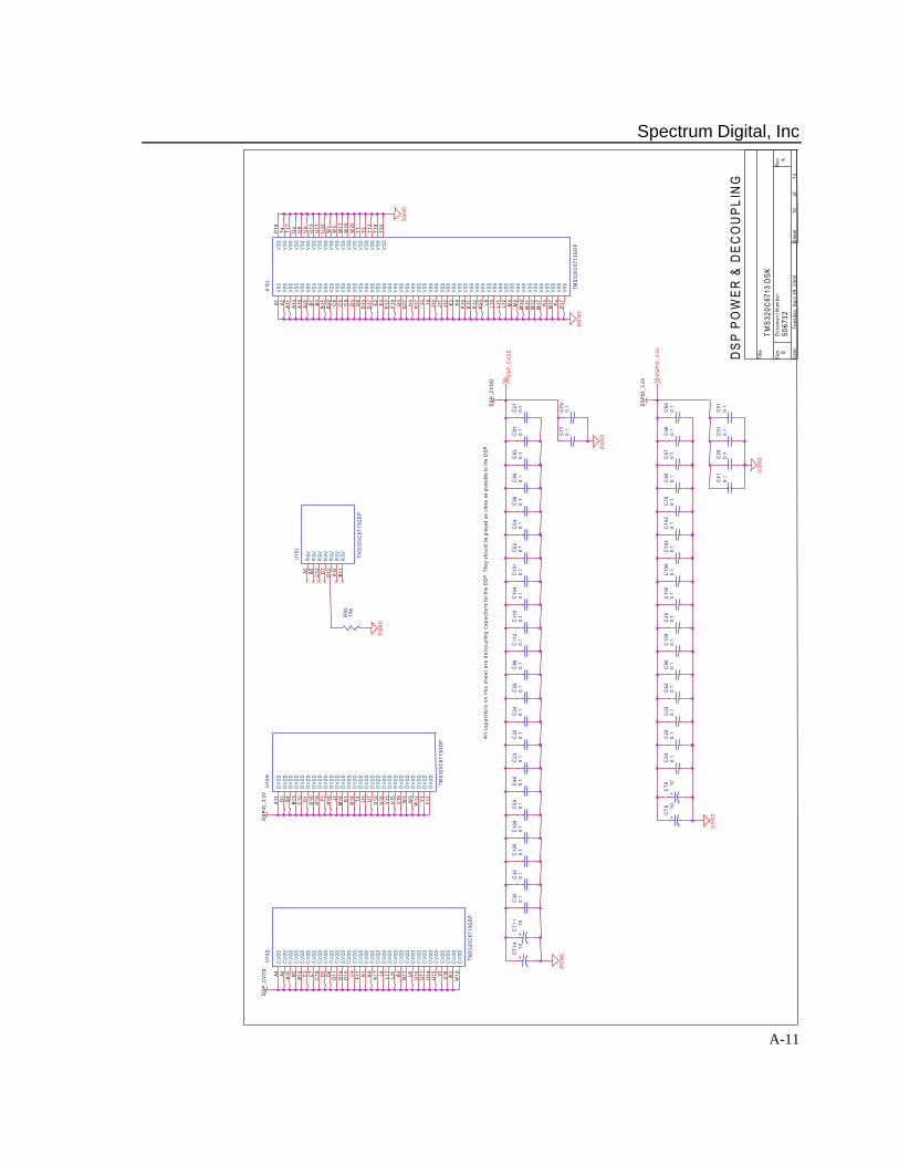
Spectrum Digital, Inc
A-11
DSP
PO
WER
& D
ECO
UPL
ING
All
capa
cito
rs o
n th
is s
heet
are
dec
oupl
ing
capa
cito
r s fo
r the
DSP
. The
y sh
ould
be
plac
ed a
s cl
ose
as p
ossi
ble
to th
e D
SP.
5067
32A
TMS3
20C6
713
DSK
B
1013
Tues
day,
Apr
il 29
, 200
3
Title
Size
Doc
umen
t Num
ber
Rev
Dat
e:Sh
eet
of
DSP
IO_3
.3V
DSP
_CVD
D
DG
ND
DG
ND
DG
ND
DS P
IO_3
.3V
DSP
IO_3
.3V
DS P
_CVD
D
DSP
_CVD
D
DG
ND
DG
ND
DG
ND
DG
ND
C77
0 .1
C79
0 .1
C51
0.1
C26
0.1
C31
0.1
U1 0
G
TMS3
20C
6713
GD
P
A4 A 9 A10 B 2 B19
C3
C7
C18 D
5D
6D
11D
14D
15 F4 F17 K 1 K4 K 17 L4 L 17
L20
R4
R1 7 U
6U
10U
11U
14U
15 V 3 V18
W2
W19
CVD
DC
VDD
CVD
DC
VDD
CVD
DC
VDD
CVD
DC
VDD
CVD
DC
VDD
CVD
DC
VDD
CV D
DC
VDD
CV D
DC
VDD
CVD
DC
V DD
CVD
DC
VDD
CV D
DC
VDD
CVD
DC
VDD
CVD
DC
VDD
CVD
DC
VDD
CVD
DC
VDD
CVD
DC
VDD
C41
0.1
C52
0.1
R6 0
10K
C10
20.
1
C11
00.
1C
880.
1
U1 0
H
TMS3
20C
6713
GD
P
A17 B 3 B8 B 13
C1 0 D
1D
16D
19 F 3 H18 J2
M18 R
1R
18 T3 U5
U7
U12
U1 6 V 1
3V1
5V1
9
W12 Y 7 Y 1
7
W3
W9
DVD
DD
VDD
DVD
DD
VDD
DVD
DD
VDD
DVD
DD
VDD
DVD
DD
VDD
DVD
DD
VDD
DV D
DD
VDD
DV D
DD
VDD
DVD
DD
V DD
DVD
DD
VDD
DV D
DD
VDD
DVD
DD
VDD
DVD
D
DVD
DD
VDD
C78
0.1
C24
0.1
C10
40.
1
U1 0
I
TMS3
20C
6713
GD
P
A1 A 2 A11
A 14
A19
A 20 B1 B4 B 15
B 20
C6
C8
C9
D4
D8
D13
D1 7 E 2 E4 E 1
7F1
9G
4G
1 7 H4
H17 J 4 J 9 J 1
0J 1
1J1
2 K 2 K9 K 10
K11
K 12
K 20 L 9 L10
L 11
L12
M4
M9
M10
M11
M12
M17 N
4N
17 P 4 P17
P19
T 4 T17
U4
U8
U9
U13
U17
U20
W1
W5
W11
W16
W20
Y1 Y 2 Y13
Y 19
Y20
VSS
V SS
V SS
VSS
VSS
V SS
V SS
V SS
VSS
V SS
V SS
VSS
VSS
VSS
VSS
V SS
V SS
VSS
V SS
VSS
VSS
VSS
V SS
VSS
V SS
VSS
V SS
VSS
V SS
VSS
V SS
VSS
VSS
VSS
VSS
VSS
VSS
VSS
VSS
VSS
VSS
VSS
VSS
VSS
VSS
VSS
VSS
VSS
VSS
VSS
VSS
VSS
VSS
VSS
VSS
VSS
VSS
VSS
VSS
VSS
VSS
VSS
VSS
VSS
VSS
VSS
VSS
VSS
VSS
C10
30.
1
C25
0.1
C62
0.1
C10
90.
1
C32
0.1
C10
80.
1C
105
0.1
C30
0.1
C58
0.1
C46
0.1
C50
0.1
C90
0.1
C34
0.1
C35
0.1
C10
10.
1
+C
T6 10C
800.
1+
CT8 10
C48
0.1
C56
0.1
+C
T14
10+
CT1
110
C85
0.1
C10
60.
1
C11
20.
1
U10
J
TMS3
20C
6713
GD
P
A 5 B5 C12 D
7D
12 A12
B 11
RSV
RSV
RSV
RSV
RSV
RSV
RSV
C33
0.1
C54
0.1
C47
0.1
C81
0.1
C27
0.1
C23
0.1
C10
00.
1
C83
0.1
C59
0.1
C29
0.1
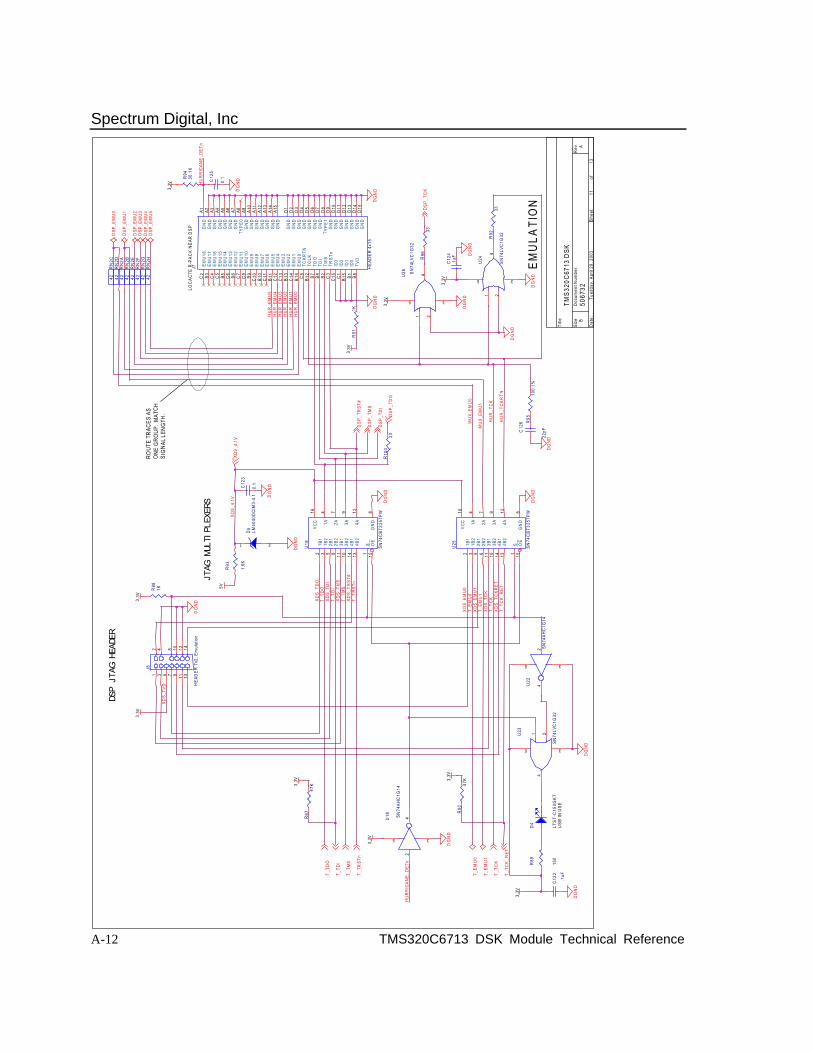
Spectrum Digital, Inc
A-12 TMS320C6713 DSK Module Technical Reference
J TAG
MUL
TIPL
EXER
S
EMU
LATI
ON
DSP
JTAG
HEA
DER
ROUT
E TR
ACES
AS
ONE
GRO
UP.
MAT
C HS I
GN A
L LE
NGTH
.
LOC
ACTE
R-P
ACK
NEA
R D
SP
USB
IN U
SE
5067
32A
TMS3
20C6
713
DSK
B
1113
Tues
day,
Apr
il 29
, 200
3
Title
Size
Doc
umen
t Num
ber
Rev
Dat
e:Sh
eet
of
X DS_
TRST
#T_
TMS
XDS_
EMU
1
X DS_
TDO
X DS_
TMS
XDS_
EMU
0
XDS_
TVD
XDS_
TDI
T_EM
U1
X DS_
4.1V
T_EM
U0
HU
RR
ICAN
E_D
ETn
HU
R_E
MU
3H
UR
_EM
U2
HU
R_E
MU
5H
UR
_EM
U4
HU
R_E
MU
1H
UR
_EM
U0
MU
X_EM
U0
MU
X_EM
U1
HU
R_T
CK
HU
R_T
CKR
TN
T_TR
STn
T_TC
K
HU
RR
ICAN
E_D
ETn
XDS_
TCKR
ET
XDS_
TCK
T_TC
K_R
ET
T _TD
O
T _TD
I
DSP
_TD
O
DSP
_TD
I
DSP
_TM
S
T_E
MU
0
T_E
MU
1
DSP
_EM
U2
DS P
_EM
U3
DSP
_EM
U5
DSP
_EM
U4
T_TC
K_R
ET
DSP
_EM
U0
DSP
_EM
U1 D
SP_T
CK
DSP
_TR
ST#
T _T M
S
T_TC
K
T_TR
STn
X DS_
4.1V
T_TD
O
T _TD
I
DG
ND
3 .3V
DG
ND
DG
ND
DG
ND
3 .3V
DG
ND
5V
DG
ND
DG
ND3.
3V
DG
ND
3 .3V
DG
ND
DG
ND
DG
ND
3 .3V
3.3V
DG
ND
3.3V
3.3V
DG
ND
DG
ND
3.3V
DG
ND
DG
ND
3.3V
RN
2C42
RN
2D42
U24
SN74
LVC
1G32
1 24
5 3
R96
33
R92
33
R93
1.6K
D5 LM
4040
DCI
M3-
4.1
21
RN
2B4 2
RN2
A42
C12
2.1
uF
R10
033
R89
150
U26 SN
74LV
C1G
321 2
4
5 3
R95
100
1%
C12
6
22pF
J8
HEA
DER
7x2
, Em
ulat
ion
1 3 5 7 9
2 4 8 101 1
1 213
14
R67
4 7K
R90
47K
C12
4.1
uF
U19
S N74
CBT
3257
PW
4
1 4
71 1
9 1 21 3 12 151 03 5 6
1 6 8
1 A
4B1
2 A3 B
13 A 4 A
4 B2
S1 B1
OE
3 B2
1 B2
2 B1
2 B2
V CC
GN
D
U25
SN74
CBT
3257
PW
4
14
711
9 1213 12 15103 5 6
1 6 8
1A
4B1
2A3B
13A 4A
4B2
S1 B1
OE
3B2
1B2
2B1
2B2
VCC
GN
D
J7 HEA
DER
4x1
5
A 1 A2 A 3 A4 A 5 A6 A7 A8 A9 A 10
A 11
A 12
A 13
A 14
A15
D1
D2
D3
D4
D5
D6
D7
D8
D9
D10
D11
D12
D13
D14
D15
B14
C14B1
3C
13 B 12
C12B 1
1C
11B 10
C10B 9C
9 B 7C7B6C6B 5C5 B4C4B3 C3B 2C2 B 1B 15
C1
C15 B 8C
8
GN
DG
ND
GN
DG
ND
GN
DG
ND
GN
DT Y
PE0
GN
DG
ND
GN
DG
ND
GN
DG
ND
GN
D
GN
DG
ND
GN
DG
ND
GN
DG
ND
GN
DT Y
PE1
GN
DG
ND
GN
DG
ND
GN
DG
ND
GN
D
E MU
0E M
U1
EMU
2E M
U3
TCLK
EMU
4E M
U5
EMU
6E M
U7
EMU
8E M
U9
EMU
10
T DO
E MU
11EM
U12
EMU
13EM
U14
E MU
15
T DI
EMU
16E M
U17
T RST
nT M
S
E MU
18
ID0
I D1
I D2
I D3
T VD
TCKR
TN
D4
LTS
T-C
150G
KT
R9 4
30.1
K
R88
1K
C12
3
0 .1
U23
SN74
LVC
1G32
1 24
5 3
U22
SN74
AHC
1G14
3
4
5
2
U18 S N
74AH
C1G
14
3
4
5
2
RN
2H42
RN
2G42
RN
2F4 2
RN
2E4 2
R91
1K
C12
5
0 .1
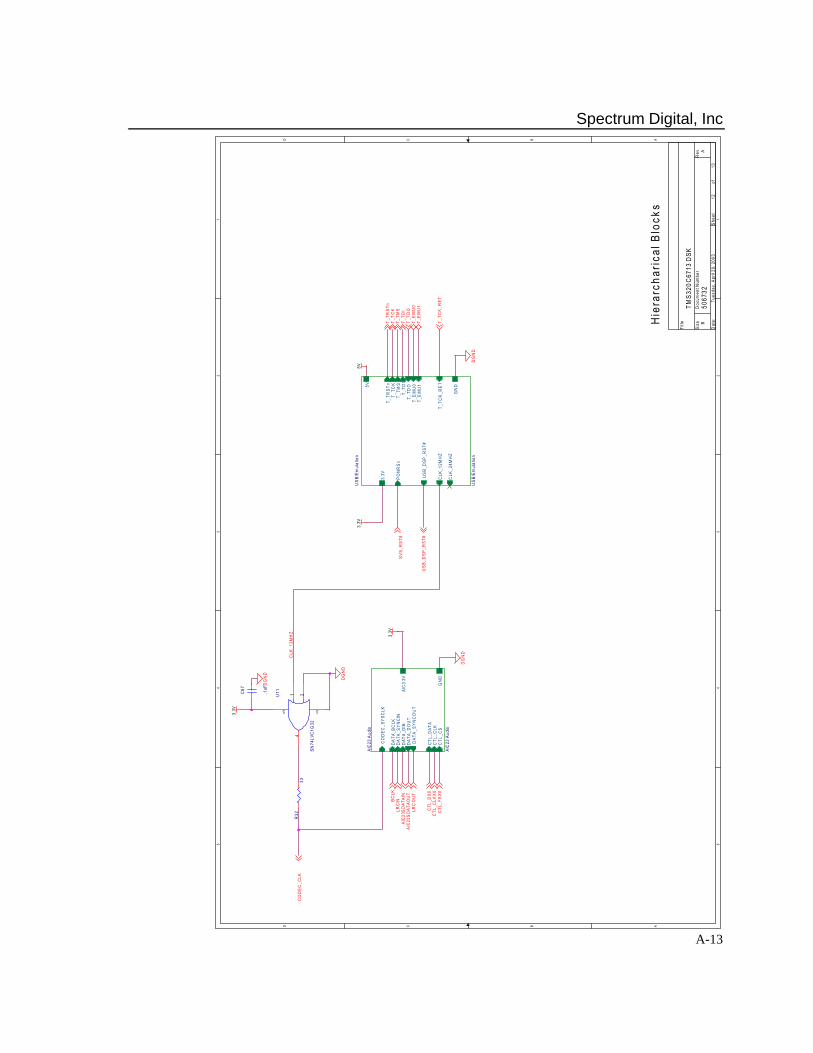
Spectrum Digital, Inc
A-13
5 5
4 4
3 3
2 2
1 1
DD
CC
BB
AA
Hier
arch
aric
al B
lock
s
5067
32A
TMS3
20C6
713
DSK
B
1213
Tues
day,
Apr
il 29
, 200
3
Title
Size
Doc
umen
t Num
ber
Rev
Dat
e:Sh
eet
of
USB
/Em
ulat
ion
USB
/Em
ulat
ion
5V
USB
_DSP
_RST
#
T_TD
O
T_TC
KT_
TMS
T_TR
STn
T_E
MU
0T_
EM
U1
T_TD
I
3.3V
PON
RSn
GN
D
T_TC
K_R
ET
CLK
_12M
HZ
CLK
_24M
HZ
AIC
23 A
udio
AIC
23 A
udio
GN
D
DAT
A_BC
LKD
ATA_
SYN
CIN
DAT
A_DI
ND
ATA_
DO
UT
CTL
_DAT
AC
TL_C
LKC
TL_C
S
CO
DEC
_SYS
CLK
AIC
3.3V
DAT
A_SY
NC
OU
T
CLK
_12M
HZ
USB
_DSP
_RST
#
T_TD
IT_
TMS
T_TC
K
T_E
MU
0T_
EM
U1
T_TD
OSV
S_R
ST#
T_TR
STn
T_TC
K_R
ETC
TL_C
LKX0
CTL
_FSX
0
CTL
_DX0
BCLK
AIC
23SD
ATAO
UT
LRC
OU
T
AIC
23SD
ATAI
NLR
CIN
CO
DEC
_CLK
5V
DG
ND
3.3V
3.3V
DG
ND
DG
ND
3.3V
DG
ND
U11
SN74
LVC
1G32
1 24
5 3
C67
.1uF
R32
33
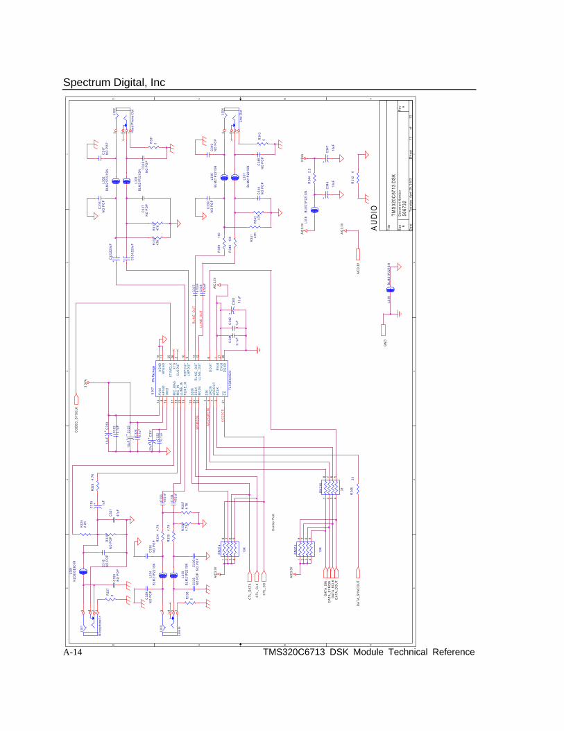
Spectrum Digital, Inc
A-14 TMS320C6713 DSK Module Technical Reference
5 5
4 4
3 3
2 2
1 1
DD
CC
BB
AA
Con
trol P
ort
AU
DIO
5067
32A
TMS3
20C
6713
DSK
B
1313
Tues
day,
Apr
il 29
, 200
3
Title
Size
Doc
umen
t Num
ber
Rev
Dat
e:Sh
eet
of
LLIN
E_O
UT
RLI
NE_
OU
T
AIC
23LR
CIN
AIC
23CS
SPIM
OD
E
3.3V
A
3.3V
A
AIC
3.3V
AIC
3.3V
AIC
3.3V
AIC
3.3V
AIC
3.3V
+
C32
510
uF
C32
60.
1uF+
C31
910
uF
C32
20.
1uF
R32
52.
2K
R32
8N
O P
OP
R32
64.
7K
R33
74.
7K
R33
44.
7K
R33
64.
7K
R33
54.
7K
C34
1
0.1u
F
+C32
3220
uF
+ C32
4220
uF
L306
BLM
21P2
21SN
C34
0N
O P
OP
C34
4N
O P
OP
C34
5N
O P
OP
R34
30
C32
1
47pF
+
C31
5
1uF
L307
BLM
21P2
21SN
C33
9N
O P
OP
C33
847
0nF
J302
Hea
d Ph
one
Out
3 4 2 1
C34
2
0.1u
F
R33
247
KC
333
470n
F
C33
447
0nF
R33
347
KJ3
03
Line
In
3 4 2 1
R34
533
C33
20.
1uF
J301
Mic
roph
one
In
3 4 2 1
+C
343
10uF
C33
747
0nF
R31
20
C33
6N
O P
OP
L305
BLM
21P2
21SN
C32
9N
O P
OP
+
C33
110
uF
J304
Line
Out
3 4 2 1
R34
1 47K
R34
2 47K
R33
910
0
R33
80
L304
BLM
21P2
21SN
C33
0N
O P
OP
C33
5N
O P
OP
RN
314
10K
1 2 3 45678
RN
316
33
1 2 3 45678
R34
010
0
PW P
acka
geU
307 TL
V320
AIC2
3
22141115 25
34 5 212423
10 9 28
16 17 18 20 19
26 13 12
8
167
2 27
MO
DE
AVdd
HPG
ND
AGND
XTI/M
CLK
BCLK
DIN
LRCI
N
CS
SCLK
SDIN
RH
POU
TLH
PO
UT
DG
ND
VMID
MIC
_BIA
SM
IC_I
NLL
INE_
INR
LIN
E_IN
XTO
RLI
NE_
OU
TLL
INE_
OU
T
HPV
dd
BVdd
DO
UT
LRC
OU
T
CLK
OU
T
DVd
d
L308
BLM
21P2
21SN
L303
BLM
21P2
21SN
C31
8N
O P
OP
R34
42.
2
L301
HZ0
805E
601R
R32
70
C32
0N
O P
OP
L309
BLM
21P2
21SN
C31
7N
O P
OP
C31
6N
O P
OP
C32
7N
O P
OP
R33
10
+C
347
10uF
+C
346
10uFL3
02BL
M21
P221
SN
C32
8N
O P
OP
RN
315
10K
1 2 3 45678
CTL
_CLK
CTL
_CS
CTL
_DAT
A
DAT
A_DI
ND
ATA_
SYN
CIN
DAT
A_BC
LKD
ATA_
DO
UT
DAT
A_SY
NC
OU
T
CO
DEC
_SYS
CLK
AIC
3.3V
GN
D
B-1
Appendix B
Mechanical Information
This appendix contains the mechanical information about theTMS320C6713 DSK produced by Spectrum Digital.

Spectrum Digital, Inc
B-2 TMS320C6713 DSK Module Technical Reference
TH
IS D
RA
WIN
G IS
NO
T T
O S
CA
LE


Printed in U.S.A., May 2003506735-0001 Rev. A