TKT-1212 Digitaalijärjestelmien toteutus · Exercises in practice Weekly exercises in TC417 (Linux...
34
Lecture 1 – Introduction Ari Kulmala Tampere University of Technology, 2008 TKT-1212 Digitaalijärjestelmien toteutus
Transcript of TKT-1212 Digitaalijärjestelmien toteutus · Exercises in practice Weekly exercises in TC417 (Linux...

Lecture 1 – Introduction
Ari Kulmala
Tampere University of Technology, 2008
TKT-1212
Digitaalijärjestelmien toteutus

Course Description Web: http://www.tkt.cs.tut.fi/kurssit/1212/
Lectures Period 3 Tuesday 10-12 TB111
Wednesday 12-14 S4 (only in december!)
Period 4: Tuesday 10-12, x
Exercises Teemu Pitkänen, Antti Alhonen, Jussi Kurki, Erno Salminen Periods 3-5 Tiistai 12-14 TC417
Keskiviikko 10-12 TC417
Torstai 10-12 TC417
Torstai 14-16 TC417
Perjantai 12-14 TC417
2 Ari Kulmala, 2008, Tampere University of Technology

Exercises
3 Ari Kulmala, 2008, Tampere University of Technology

Overview
Project work of the course is a simple audio synthesizer implemented on FPGA Each of the four buttons produces
different tone Sound is heard from the external
speakers
During this project work, you will learn to describe and verify digital systems
using VHDL De facto standard in European
microelectronic industry
to operate Wolfson audio codec chip (also used in some iPods)
to use I2C bus developed by Philips. Lightweight serial bus used for example
in car industry
4 Ari Kulmala, 2008, Tampere University of Technology

Exercises in practice Weekly exercises in TC417 (Linux class) Project work done piece by piece Done alone or in groups of two Five guidance sessions Tuesday- Friday Presence is not required Return is mandatory, email to [email protected]
Each exercise is returned within two weeks (due Sunday 23:59)
The first exercise on week 50, 9.-12.12. On the first week, presence is mandatory More information available at the first exercise
Possibility to gain 6 bonus points to the passed exam
You must report person hours for each exercise
5 Ari Kulmala, 2008, Tampere University of Technology

Action points
1. Apply for a Birdland account if you do not have one
http://www.cs.tut.fi/lintula/
2. Fill and sign Access application and confidentiality agreement
Return the form to TH305 (Timo Rintakoski)
3. Register to one of the exercise groups
4. Optional: You may install the needed SW tools to your
home computer
5. Optional: You may borrow an Altera DE2 FPGA board
6 Ari Kulmala, 2008, Tampere University of Technology

Course Goals Get to know Practical Digital system design
Aware of Challenges of Digital system design
Design for efficiency
Design for large scale
Large module, large system, overall development process
Design for portability
Device independency, software dependency, design reuse
7 Ari Kulmala, 2008, Tampere University of Technology

Course Description #2 Course requirements:
Regular exam or two midterm exams
Succesful exercises/exercise work
Course primarily based on book:
RTL Hardware Design Using VHDL: Coding for Efficiency,
Portability, and Scalability. Chu, Pong P. (2006)
Can be loaned from the lecturer
Available at TUT library
Snippets from other sources also
Available from the lecturer
Lectures and lecture notes should be enough for passing the course
8 Ari Kulmala, 2008, Tampere University of Technology

Course contents
VHDL
Very High Speed Integrated Circuit Hardware Description
language = VHSIC HDL = VHDL
Familiarize with the language constructs
Efficient, portable coding
System integration issues
Testbenches and simulators
Guidelines for re-use
FPGA circuits, designing for FPGA
Clock synchronization, multiple clock domains
9 Ari Kulmala, 2008, Tampere University of Technology

Schedule
10 Ari Kulmala, 2008, Tampere University of Technology
# AIKA PAIKKA AIHE
1 2.12.2007 Ti 10-12 TB111 Kurssin järjestelyt, johdanto
2 3.12.2007 Ke 12-14 S4 Johdanto, VHDL-perusteet #1, entities, architectures
3 9.12.2007 Ti 10-12 TB111 VHDL-perusteet #2 - prosessit, signaalit, tyypit
4 10.12.2007 Ke 12-14 S4 VHDL-perusteet #3 - packages, libraries, operators, attributes
5 16.12.2007 Ti 10-12 TB111 VHDL combinational and sequential part design, generics, statements
6 17.12.2007 Ke 12-14 S4 Synthesis, FSM implementation
7 13.1.2008 Ti 10-12 TB111 VHDL testbenches
8 20.1.2008 Ti 10-12 TB111 HDL Simulators
viikko 5 tenttiviikko
12 3.2.2008 Ti 10-12 x HDL Re-use, Coding guidelines
9 10.2.2008 Ti 10-12 x FPGA devices in general
10 17.2.2008 Ti 10-12 x
Real-life FPGA: Altera Stratix III, case study SDRAM
11 24.2.2008 Ti 10-12 x Multiple clock domain circuits, synchronization
13 3.3.2008 Ti 10-12 x System design challenges
14 10.3.2008 Ti 10-12 x Vierailuluento:
Viikko 12 tenttiviikko / välikoe
15 24.3.2008 Ti 10-12 x 1. välikokeen käsittely, Kertaus (?)
Introduction
11 Ari Kulmala, 2008, Tampere University of Technology
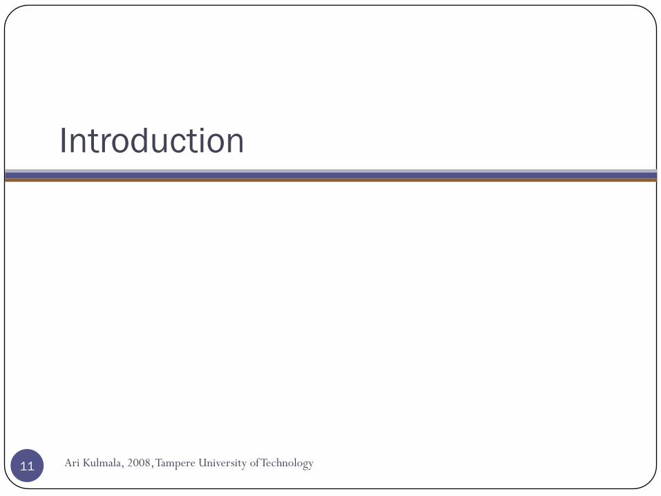
Digital Circuits Nowadays found everywhere
From simple microcontrolles in wash machines to space shuttles
Digital circuits are typically integrated circuits (IC)
Minimize the number of discrete components
Typical digital systems, such as cellular phones, contain
(Several) Processors and co-processors
Application-specific hardware
An on-chip interconnection between the components
Memory RAM, FLASH, even hard disks
RF/Analog IC Out of the scope of this course
12 Ari Kulmala, 2008, Tampere University of Technology

How to implement a digital system
No two applications are identical and every one needs certain amount of customization
Basic methods for customizationa) ―General-purpose hardware‖ with custom software General purpose processor: e.g., performance-oriented processor (e.g., Pentium),
cost-oriented processor (e.g., PIC micro-controller)
Special purpose processor: architecture with a specific set of functions: e.g., DSP processor (to do multiplication-addition), network processor (to do buffering and routing), ―graphic engine‖ (to do 3D rendering)
b) Custom hardware (no software)
c) Custom software on a custom platform (CPU+other hardware) (known
as hardware-software co-design)
13 Ari Kulmala, 2008, Tampere University of Technology

How to implement a digital system (2)
Trade-off between flexibility, programmability, design
effort, cost, performance, and power consumption
A complex application contains many different tasks and
use more than one customization methods
14 Ari Kulmala, 2008, Tampere University of Technology

2. Device Technologies
15 Ari Kulmala, 2008, Tampere University of Technology
TKT-1212 Dig.järj.tot., syksy 2008, A. Kulmala, TTY
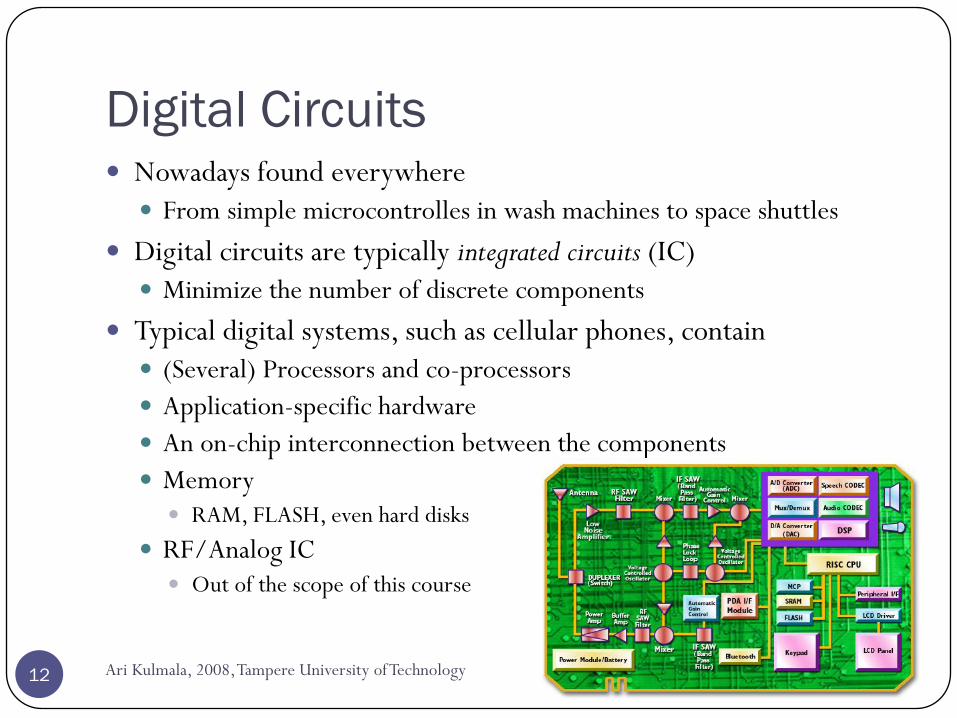
What does an IC look like?
transistors
• Wires on top levels
are wider and
taller than on
lower levels
• Top layers for
• Power supply
• Clock
• Global signals
Several metal layers
Less congention
Hierarchical scaling
ITRS 2003: Interconnect Chip cross-section

What does an IC look like? (2)
Ari Kulmala, 2008, Tampere University of Technology18
Intel Penryn
dual core.
The IC
Package
http://www.intel.com/pressroom/kits/45nm/photos.htm
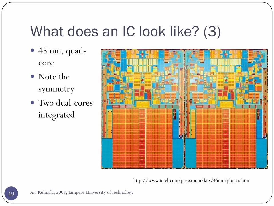
What does an IC look like? (3)
Ari Kulmala, 2008, Tampere University of Technology19
45 nm, quad-
core
Note the
symmetry
Two dual-cores
integrated
http://www.intel.com/pressroom/kits/45nm/photos.htm

What does an IC look like (3)
Ari Kulmala, 2008, Tampere University of Technology20
Actel Fusion Mixed-signal FPGA
1. Integrated Analog-to-Digital Converter (ADC)
2. Fusion Supports Low Power, synchronization
3. Embedded Flash Memory
4. Advanced I/O Standards
5. Charge Pumps
6. Analog Quads
7. Flash FPGA VersaTile
8. SRAM and FIFOs
9. Integrated Oscillators—Crystal and RC
10. Routing Structure
11. JTAG
http://www.actel.com/documents/Fusion_PIB.pdf

Classification of device technologies
Where customization is done: In a fab (fabrication facility): ASIC (Application
Specific IC) Full-custom ASIC Standard cell ASIC Gate array ASIC
In the ―field‖: non-ASIC Complex field programmable logic device Simple field programmable logic device Off-the-shelf SSI (Small Scaled IC)/MSI (Medium Scaled IC) components
21 Ari Kulmala, 2008, Tampere University of Technology

Full-custom ASIC
All aspects (e.g., size of a transistor) of a circuit are tailored for a particular application.
Circuit fully optimized
Design extremely complex
Very time consuming design (Typically only feasible for small components)
Masks needed for all layers
Very expensive
Fabrication time up to months
Example: Intel and AMD processors are (partly) full-custom
22 Ari Kulmala, 2008, Tampere University of Technology

Standard-Cell ASIC
Circuit made of a set of pre-defined logic, known as standard cells
E.g., basic logic gates, 1-bit adder, D FF etc
Library cannot be altered albeit some basic parameters
Layout of a cell is pre-determined, but layout of the complete circuit is customized
The location of the standard cells
Connections between cells
Masks needed for all layers
Same fabrication cost as with full custom
Eg. Mobile phone digital ICs
23 Ari Kulmala, 2008, Tampere University of Technology

Gate array ASIC
Circuit is built from an array of a single type of cell (known as base cell)
Base cells are pre-arranged and placed in fixed positions, aligned as one- or two-dimensional array
Connections customized
More sophisticated components (macro cells) can be constructed from base cells
Masks needed only for metal layers (connection wires)
Cheaper than full custom or standard cell
24 Ari Kulmala, 2008, Tampere University of Technology
Complex Field Programmable Logic Device
Device consists of an array of generic logic cells and general interconnect structure
Logic cells and interconnect can be ―programmed‖ by utilizing ―semiconductor fuses‖ or ―switches‖
Customization is done ―in the field‖
Two categories: CPLD (Complex Programmable Logic Device) sea-of-gates to implement logic
FPGA (Field Programmable Gate Array) Look-up tables to implement logic
No custom mask needed
For example, Cisco 2600 series routers
25 Ari Kulmala, 2008, Tampere University of Technology

Simple Field Programmable Logic Device
(PLD)
Programmable device with simple internal structure
E.g.,
PROM (Programmable Read Only Memory)
PAL (Programmable Array Logic)
No custom mask needed
Outdated
Replaced by CPLD/FPGA
26 Ari Kulmala, 2008, Tampere University of Technology

SSI/MSI components
Small discrete parts with fixed, limited functionality
E.g. AND-ports in Printed Circuit Board (PCB)
E.g., 7400 TTL series (more than 100 parts)
Resource (e.g., power, board area, manufacturing cost etc.) is
consumed by package but not silicon
No longer a viable option!
Hobby projects
27 Ari Kulmala, 2008, Tampere University of Technology

Three viable technologies
Standard Cell ASIC
TKT-1400 ASIC-suunnittelu I
Gate Array ASIC
TKT-1400 ASIC-suunnittelu I
FPGA/CPLD
This course
28 Ari Kulmala, 2008, Tampere University of Technology

Comparison of technology
Area (Size): silicon real-estate: [mm2], [eq. gates]
Speed (Performance): [MHz], [op/s] Operations/second
i.e. Time required to perform a task
Power consumption [mW]
Cost [€]
Design effort [person-month]
29 Ari Kulmala, 2008, Tampere University of Technology

Comparison of technology
Ari Kulmala, 2008, Tampere University of Technology30
Area: ASIC (sc) vs FPGA
Standard cell is the smallest since the cells and interconnect are customized
FPGA is the largest Overhead for programmability
Capacity cannot be completely utilized
Roughly: FPGA is approximately 35 times larger using the LUT-
based logic elements [1]
However, that is not seen by FPGA end users – high volume compensates
some costs ($$)
Performance: ASIC (sc) vs FPGA
Roughly: FPGA is between 3.4 to 4.6 times slower, MHz [1]
[1] I. Kuon and J. Rose, "Measuring the Gap between FPGAs and ASICs" in
IEEE Transactions on Computer-Aided Design of Integrated Circuits and
Systems, Vol. 26, NO. 2, FEBRUARY 2007, pp. 203 - 215.

Cost
Types of cost:
Chip design costs NRE (Non-Recurring Engineering) cost: one-time, per-design cost
Part cost: per-unit cost
Indirect design costs Lead time: time to get the chip out of the factory
Time-to-market ―cost‖ loss of revenue
Standard cell: high NRE, small part cost and large lead time
FPGA: low NRE, large part cost and small lead time
31 Ari Kulmala, 2008, Tampere University of Technology

ASIC cheaperFPGA cheaper
Cost of Integrated Circuits (4)
Ari Kulmala, 2008, Tampere University of Technology
For ASIC, first-time-right necessary
FPGA has lower NRE, but higher RE Suitable for low volumes
Break even volume getting bigger all the time
cost
[€]
#chips
break even
ASIC
FPGA
trend
Xilinx Inc.
faster growth rate
than with ASIC
32

Graph of per-unit cost
33 Ari Kulmala, 2008, Tampere University of Technology

Summary of technologies
Trade-off between optimal use of hardware resource and design effort/cost
No single best technology
34 Ari Kulmala, 2008, Tampere University of Technology

Conclusions
Ari Kulmala, 2008, Tampere University of Technology35
Two viable implementation technologies: ASIC and FPGA
ASICs are smaller in area and faster than FPGA
ASICs have low unit cost but high NRE, FPGA vice versa
ASICs used in high volume products, FPGAs in tailorable
products
FPGA is a ‖programmable ASIC‖ (custom IC, actually)
i.e. someone has done an IC which application is FPGA
Extra resources needed to provide in-field configuration


![TKT-1212 Digitaalijärjestelmien · PDF fileTKT-1212 Digitaalijärjestelmien toteutus ... Schedule slip is 5-30% [Accenture’s report] or even 44% ... Cellular phones as embedded](https://static.fdocuments.in/doc/165x107/5a9f93717f8b9a7f178cfa4f/tkt-1212-digitaalijrjestelmien-digitaalijrjestelmien-toteutus-schedule-slip.jpg)