Thyristors - Theory, Parameters and Application s
21
1 THYRISTOR APPLICATIONS INFORMATION Thyristors - Theory, Parameters and Applications Jurek Budek Bedford Applications Laboratory (Edited by M J Maytum) Bedford Power Department ABSTRACT The operational characteristics of the Thyristor are derived from the basic silicon structure and its equivalent circuit. Actual device character- istics and ratings are then discussed with illustrations of the temperature and operating mode sensitivities. Based on this, design approaches are formulated for triggering, selection and control of current and voltage, finishing with cooling requirements. Finally, some typical applica- tion circuits are discussed INTRODUCTION The name of Thyristor is derived from the Greek word "ηθνρα" meaning "a door". A Thyristor is a bistable semiconductor device that comprises three or more junctions and can be switched from the off state to the on state or vice versa. Switching from the off state to the on state is normally initiated by a control signal. Switch off is normally caused by the current though the Thyristor dropping below a critical level. This chapter is concerned with the two main Thyristor types called SCRs (Silicon Controlled Rectifiers - Ref. 1.) and Triacs (Ref. 2.). Chapter 2, Glossary, should be consulted for further information on types, terms and definitions. The first commercial SCRs appeared in the late 1950s. They were an immediate success by providing an efficient, long life, bounceless switch to replace relays, rheostats, thyratrons and such like. The SCR is a unidirectional Thyristor and so it can only be controlled in one voltage polarity. To control both polarities of the ac supply either two SCRs had to be used, con- nected in anti-parallel, or a single SCR inside a full wave bridge rectifier (Ref. 1, Chapter 8 - AC Phase Controlled Circuits). In the 1960s, bidirectional Thyristors, called Triacs, where introduced. AC control was now possible with a single silicon power device. Today, through better understanding and technology, SCRs, Triacs and their derivatives are pre-eminent in the solid state control of ac power. THEORY BIPOLAR JUNCTION HIERARCHY The Thyristor NPNP silicon layer structure can be considered the result of an evolution the basic PN layer junction rectifier diode, Figure 1. The following treatment of bipolar junction behaviour assumes readers are familiar with basic semiconductor theory. Diodes A PN junction diode has a low impedance when the P-type layer is positively (forward) voltage biased with respect to the N- type layer. The electrode connecting to the P-type layer is called the anode, symbol A, and that connecting to the N-type layer is called the cathode, symbol K. Forward conduction begins at a threshold voltage of about 0.5 V and a junction strongly in current conduction will develop voltages of 0.7 V and above. The direction of this current conduction is indicated by the arrow direction of the diode symbol. The diode has a high impedance when the P-type layer is negatively (reverse) voltage biased with respect to the N-type layer. The maximum value of reverse voltage that the junction blocks to will depend on the junction design. Above this voltage the junction will breakdown, symbol (BR), either at the surface or internally. Internal breakdowns below about 6 V are due to the "Zener" effect and above 6 V by the "Avalanche" effect. Zener voltages decrease with increasing temperature, whilst Ava-
Transcript of Thyristors - Theory, Parameters and Application s

1
THYRISTOR APPLICATIONS INFORMATION
Thyristors - Theory, Parameters and Applications
Jurek BudekBedford Applications Laboratory
(Edited by M J Maytum)Bedford Power Department
ABSTRACT
The operational characteristics of the Thyristor are derived from the basic silicon structure and its equivalent circuit. Actual device character-istics and ratings are then discussed with illustrations of the temperature and operating mode sensitivities. Based on this, design approaches are formulated for triggering, selection and control of current and voltage, finishing with cooling requirements. Finally, some typical applica-tion circuits are discussed
INTRODUCTION
The name of Thyristor is derived from the Greek word "ηθνρα" meaning "a door". A Thyristor is a bistable semiconductor
device that comprises three or more junctions and can be switched from the off state to the on state or vice versa. Switching from the off state to the on state is normally initiated by a control signal. Switch off is normally caused by the current though the Thyristor dropping below a critical level. This chapter is concerned with the two main Thyristor types called SCRs (Silicon Controlled Rectifiers - Ref. 1.) and Triacs (Ref. 2.). Chapter 2, Glossary, should be consulted for further information on types, terms and definitions.
The first commercial SCRs appeared in the late 1950s. They were an immediate success by providing an efficient, long life, bounceless switch to replace relays, rheostats, thyratrons and such like. The SCR is a unidirectional Thyristor and so it can only be controlled in one voltage polarity. To control both polarities of the ac supply either two SCRs had to be used, con-nected in anti-parallel, or a single SCR inside a full wave bridge rectifier (Ref. 1, Chapter 8 - AC Phase Controlled Circuits).
In the 1960s, bidirectional Thyristors, called Triacs, where introduced. AC control was now possible with a single silicon power device. Today, through better understanding and technology, SCRs, Triacs and their derivatives are pre-eminent in the solid state control of ac power.
THEORY
BIPOLAR JUNCTION HIERARCHY
The Thyristor NPNP silicon layer structure can be considered the result of an evolution the basic PN layer junction rectifier diode, Figure 1. The following treatment of bipolar junction behaviour assumes readers are familiar with basic semiconductor theory.
Diodes
A PN junction diode has a low impedance when the P-type layer is positively (forward) voltage biased with respect to the N-type layer. The electrode connecting to the P-type layer is called the anode, symbol A, and that connecting to the N-type layer is called the cathode, symbol K. Forward conduction begins at a threshold voltage of about 0.5 V and a junction strongly in current conduction will develop voltages of 0.7 V and above. The direction of this current conduction is indicated by the arrow direction of the diode symbol.
The diode has a high impedance when the P-type layer is negatively (reverse) voltage biased with respect to the N-type layer. The maximum value of reverse voltage that the junction blocks to will depend on the junction design. Above this voltage the junction will breakdown, symbol (BR), either at the surface or internally. Internal breakdowns below about 6 V are due to the "Zener" effect and above 6 V by the "Avalanche" effect. Zener voltages decrease with increasing temperature, whilst Ava-

THYRISTOR APPLICATIONS INFORMATION
2
lanche voltage increase at approximately 0.1%/°C. When the breakdown is internal, reasonable amounts of breakdown power can be reliably dissipated. This, together with a low impedance in the breakdown condition, is the basis of reference/regulator/Zener diodes. Such diodes are indicated by a "hook" on the diode crossbar.
Both majority and minority carriers take part in the forward conduction (bipolar action). This causes conduction delays. A fast rising forward conduction current may initially cause a forward voltage higher than the dc value. More importantly, as the con-
duction current reverses, the stored charge in the diode prevents instantaneous switching back to the reverse-blocking state.
Transistors
Adding a second junction creates the bipolar junction transistor, Figure 2. Depending where the second junction is added the transistor can be a PNP or a NPN layer device. Figure 2, shows the structure of an NPN transistor. By making a thin central base layer, the majority of the carriers injected from the emitter layer travel straight through the base layer and into the collec-tor layer. The uncollected carriers form the base current, IB. For injection to take place the base-emitter junction must be for-
ward biased, but the base current needed to establish the bias is much smaller than the collector current, IC. Thus the bipolar
transistor is considered as a current amplifier with a gain, HFE, of IC/IB.
The voltage drop across the base-emitter junction will be similar to a diode, 0.5 V threshold and 0.7 V or above when in full conduction. The transistor symbol marks the base-emitter junction with an arrow in the emitter, the arrow being oriented to show the direction of current flow. An NPN transistor has the arrow pointing away from the base and a PNP transistor has the arrow pointing to the base. Although the base-collector junction is another diode, the normal direction of collector current flow is in the same direction as the emitter current flow, i.e. in the opposite direction to the current flow of a forward biased base-collector junction.
When the external circuit does not allow the transistor to pass its full value of collector current, the current difference is added to the base current. The relative increase in base current lowers the transistors gain, IC/IB, and the transistor is said to be in sat-
uration, symbol (SAT). Under these conditions the base-collector junction starts to become forward biased, which reduces its collection efficiency. If the base-collector junction is at the threshold of forward conduction, 0.5 V, and the base-emitter junc-tion saturation voltage, VBE(SAT),is 0.7 V, the collector-emitter saturation voltage, VCE(SAT), will be the voltage difference of
Figure 1. Diodes
AITHAA
P
N
ANODETERMINAL
CATHODETERMINAL
ANODE
CATHODE
REVERSE-BLOCKINGSTATE
V
I
FORWARD-CONDUCTING
STATE

3
THYRISTOR APPLICATIONS INFORMATION
the two junction drops, i.e. VCE(SAT) = 0.7-0.5 = 0.2V. When in saturation large amounts of stored charge are developed which
delays the transistor switch off.
Unidirectional Thyristors (SCR)
Adding a fourth layer creates an NPNP layer structure Figure 3. For anode voltages negative with respect to the cathode, the PN junction connected to the anode blocks any current flow until the breakdown condition is reached. When a positive voltage is applied, the PN junction connected to the gate blocks any current flow until a junction breakdown condition is reached. In this polarity the breakdown voltage is not sustained, but switching into a low voltage state occurs (condition "a" in Figure 3.). This low voltage on-state condition is maintained until the current falls below a critical value called the holding current. The SCR may also be switched on below the breakdown voltage by applying a control current to the gate (curve "b" in Figure 3 where the anode is at an off-state bias of V1).
This structure is normally analysed as an NPN transistor, TR1, and a PNP transistor, TR2, connected such that they share a common collector-base junction. The outer N layer forms the emitter of the NPN transistor, called the Thyristor cathode, and the outer P layer forms the emitter of the PNP, called the Thyristor anode. This connection of the two transistors forms a regen-erative loop with the collector current of the NPN supplying the base current of the PNP and the collector current of the PNP supplying to the base current of the NPN. This configuration causes the Thyristor to act as a switch - either off or on.
To initiate switch conduction current must be applied to a transistor base region. Connections to the base regions, gates, allow externally applied currents to initiate switch on. Normally, the NPN transistor base is connected to and this forms a P-type gate, or simply "gate". The control current direction is into the gate and the gate voltage value will be a transistor VBE. There
are some SCRs where connection is made to the base of the PNP transistor, forming an N-type gate. In this case the control current direction is out of the gate.
If an external base current of IB(NPN) was supplied to the NPN transistor its unlimited collector current would be
HFE(NPN)*IB(NPN) which would be the base current of the PNP transistor. The PNP transistor would amplify this current by
HFE(PNP) and supply a current of HFE(PNP)*HFE(NPN)*IB(NPN) back to the base of the NPN transistor. For the transistor pair to
Figure 2. Transistors
P
N
COLLECTORTERMINAL
EMITTERTERMINAL
BASETERMINAL
N N
NPNTRANSISTOR
EMITTER
COLLECTOR
NPN TRANSISTORBASE
EMITTER
COLLECTOR
PNP TRANSISTORBASE
COMPLEMENTARYVERSION
VCE
IC
VCE(SAT)
IB
AITHAB
THYRISTOR APPLICATIONS INFORMATION
4
remain permanently conducting the externally supplied NPN base current must be zero, satisfying the relationship:-
IB(NPN) - HFE(PNP)*HFE(NPN)*IB(NPN) <= 0
or
1 - HFE(PNP)*HFE(NPN) <= 0
The values of HFE(PNP)and HFE(NPN) will be current and temperature dependent. At low currents the HFE product falls with
reducing current until it is below unity and the SCR switches off. As mentioned earlier, the switch-off current level is called the holding current.
In addition to voltage breakdown and external gate current induced switch on, the SCR may also be switched on as a result of rapid voltage rise, dv/dt. The dv/dt causes the junction capacitance, C, to pass a displacement current of C*dv/dt into the tran-sistor bases. Values of 100 V/µs and 50 pF would cause a current of 5 mA. SCR dv/dt ratings can be increased by integrating a resistance, R, across the gate junction to bypass the capacitive current. For this example, with a gate threshold voltage of 0.5 V, a resistor value of below 100 Ω would need to be integrated. As this resistor will also bypass dc, the holding current will be increased by about 5 mA.
In the on state, TR1 and TR2 will be operating in a saturated condition. The anode to cathode voltage will be the sum of one transistors VBE(SAT) and the others VCE(SAT). This means that the on-state voltage will be about 0.7 + 0.2 = 0.9 V. The SCR
will typically switch into the on state in 1 µs, but stored charge will normally result in switch off times in 5 to 50 µs region.
Figure 3. SCRs
AR061AC
P-TYPEGATE
N-TYPEGATE
ANODE
CATHODE
P
P
N
ANODETERMINAL
GATETERMINAL
N N
CATHODE
ANODE
P-TYPEGATE
C
RTR1
TR2
OFF STATE
ON STATE
BREAKOVERVOLTAGE,CURRENT
REVERSE-BLOCKING STATE
REVERSEBREAKDOWN
THIRD QUADRANTANODE-
FIRST QUADRANTANODE+
V
I
HOLDINGCURRENT
+V1
ab
CATHODETERMINAL
5
THYRISTOR APPLICATIONS INFORMATION
Gate control will be normally lost once switching occurs.
In summary, the SCR is a three terminal device which conducts current in one direction only. It is triggered into conduction by positive gate current, when the anode is at a positive potential. Gate control is lost once switching occurs and conduction ceases when the current drops below the holding current. Turn on is rapid, but turn off is an order of magnitude slower.
Bidirectional Thyristors (Triacs)
Bidirectional Thyristors are formed by integrating two NPNP structures in antiparallel (Figure 4.). Anode and cathode terminal designations have no meaning for this structure. The terminals which conduct the switched current are called the main termi-nals. Main Terminal 1, MT1, is the reference terminal and the gate control circuit return connection is made to this terminal. Main Terminal 2, MT2, is the other main terminal. The circuit symbol for a Triac is shown in Figure 4.
In terms of voltage-current characteristics the Triac looks like two SCRs connected in anti-parallel, permitting switching in both voltage polarities. The Triac structure shows that the Main Terminal 1 has NPNP and PNPN paths to the Main Terminal 2, permitting positive and negative current flow when the appropriate SCR section is switched. In the equivalent circuits, the path for NPNP conduction is represented by TR1 and TR2, while the path for PNPN conduction is represented by TR4 and TR5.
The gate electrode connects to both N-type and P-type regions. This enables the Triac to be switched on with only one gate ter-minal, for positive or negative Main Terminal 2 voltage and with any polarity of gate current. The triggering operation is com-plicated, and the equivalent circuits are also shown for positive and negative Main Terminal 2 voltage polarities. The resistive components are formed by the resistance of the P-type and N-type layers. Shunting resistances are produced by the shorting produced by the Gate and Main Terminal electrodes. Triggering paths from the N-type and P-type gate regions are indicated by the dotted boxes. The triggering transistors, TR3 and TR6 through to TR8 are formed by the gate regions and the antiparallel SCR layers.
When the Main Terminal 2 voltage is positive the Thyristor structure formed by TR1 and TR2 can be directly triggered by a positive gate current via the series resistance into the base of TR1. The gate voltage value will be a transistor VBE plus any
resistive voltage drops. Negative gate current triggering is also possible. In this case TR3 operates in a common base configu-ration and feeds current to the base of TR2. Here the gate voltage value will be a transistor VBE plus any resistive voltage
drops.
When the Main Terminal 2 voltage is negative the Thyristor structure formed by TR4 and TR5 can be triggered by a negative gate current which flows through TR6, operating in common base configuration, and into the base of TR4. The gate voltage value will be a transistor VCE(SAT) plus a VBE. Positive gate current triggering is also possible, but the mechanism is complex
and high levels of trigger current are needed. In this case, the positive gate current switches TR7 on and its collector then con-nects the base of TR8 to Main Terminal 1. In this condition, some of the positive gate current will be fed to the base of TR5 by TR8 operating in common base configuration. The gate voltage value will be a transistor VCE(SAT) plus a VBE.
The Triac should only conduct when triggered by the gate control current. The integrated structure of the Triac means that charge from the conducting section can reduce the dv/dt withstand of the non-conducting section. This can result in uncon-trolled conduction of the Triac. The commutating dv/dt, dvc/dt, is the measure of the device performance under these condi-
tions. It is defined as the maximum rate of rise of principal voltage that will not cause switching from the off-state to the on-state immediately following on-state current conduction in the opposite quadrant. This parameter is particularly importantwith inductive loads, as these cause rapid rates of voltage rise.
In summary, the Triac is a three terminal device which conducts current in either direction. It may be triggered into conduction by any polarity of gate current for either polarity of Main Terminal 2 voltage. Similar to an SCR, gate control is lost once switching occurs and conduction ceases when the current drops below the holding current. The rate of voltage rise under inductive load conditions needs to be lower than the commutating dv/dt. Triacs offer simplified circuitry over two Thyristors as only one device and gate trigger circuit are needed.

THYRISTOR APPLICATIONS INFORMATION
6
Figure 4. Triacs
MT2TERMINAL
MT1TERMINAL
GATETERMINAL
N
P
P
N
N
P
P
N
N
PMAIN TERMINAL 2
MAIN TERMINAL 1
GATE
BREAKOVERVOLTAGE,CURRENT
V
I
THIRD QUADRANTMAIN TERMINAL 2-
FIRST QUADRANTMAIN TERMINAL 2+ON STATE
ON STATE
OFF STATE
BREAKOVERVOLTAGE,CURRENT
-V1
+V1
OFF STATEab
ba
AR061AF
P-TYPEGATE
SECTION
TR1
MT2
MT1
GATE
N-TYPEGATE
SECTION
TR2
TR3R1
TR4
MT2
MT1
GATE
P-TYPEGATE
SECTION
N-TYPEGATE
SECTION
TR5TR6
R1
TR7
TR8
THIRD QUADRANTMAIN TERMINAL 2-
FIRST QUADRANTMAIN TERMINAL 2+

7
THYRISTOR APPLICATIONS INFORMATION
PARAMETERS
The selection of a Thyristor normally starts with the necessary voltage and current ratings determined from the nature of the load and its supply voltage (See Chapter 1, Selection Guide). Some loads will draw currents that vary with time, e.g. motor locked, starting and running currents. Device capabilities for such conditions can be assessed by reference to the surge current versus time curves. Inductive loads can produce rapid voltage rises and some form of dv/dt parameter will be needed.
The final device selection will depend on the relative importance of factors such as available cooling, triggering power, pack-age and cost.
SCRs
This section covers the key parameters of SCRs. To illustrate the selection and design procedure graphs and values from the TIC126 data sheet will be used.
Voltage Ratings
The theory section explained how SCRs can be triggered into conduction by breakdown triggering in the positive polarity. This overvoltage protection mechanism does not happen in the reverse direction and the SCR can be damaged by reverse over-voltage transients. Thus the SCR should be selected on the peak repetitive reverse voltage rating, VRRM, rather than the peak
repetitive off-state voltage, VDRM. Most of the SCRs in chapter 3 are available in voltages from 400 V to 800 V. The 400 V
minimum value provides adequate safety margin on transient filtered 230 V (325 V maximum) ac supplies. In circuits where the SCR has series rectifier diodes to block reverse voltages, the voltage selection can be made on the VDRM requirements.
Current Ratings
The SCR average current rating, IT(AV), will be selected to be equal or greater than the normal load current. Where the load can
draw higher short term currents, the ability of the SCR to survive these can be determined from graphs of on-state current ver-sus current duration, See Figure 5.
Operating Temperature
Adequate cooling must be provided to ensure long term thermal stability. An estimate of the SCR power loss can be made from the power loss curve, See figure 6. This curve is plotted for continuous current, IT, and a conservative estimate of the
equivalent average on-state current (180° conduction angle), IT(AV), can made from IT(AV), = 0.6*IT. If the expected average
SCR current was 3.5 A, this would be power equivalent to a continuous current of about 6 A. The loss at this current is 8 W. This loss level is for a junction temperature, TJ, of 110°C, and if the highest ambient temperature, TA, is 40°C, the maximum
junction to ambient thermal resistance, RθJA, will be:
RθJA= (110 - 40)/8 °C/W
= 8.75°C/W
As the junction to case thermal resistance, RθJC, of the TIC126 is 2.4°C/W, the mounting and heat sink thermal resistance must
not exceed 8.75 - 2.4 = 6.35°C/W.
THYRISTOR APPLICATIONS INFORMATION
8
This requirement could be met by a simple square aluminium heat sink plate of 9 cm x 9 cm.
Triggering
The typical temperature variation of gate trigger voltage and current are shown in Figures 7 and 8. Compared to 25°C, at 0°C the voltage has increased by 10% and the current by 30%. The data sheet maximum values at 25°C are 1.5 V and 20 mA. A trigger circuit designed to work down to 0°C should provide a gate current drive of 20*1.3 = 26 mA at a voltage of 1.5*1.1 = 1.65 V. After allowing for trigger circuit tolerances, a design giving a nominal drive of 30 mA into 2 V should be adequate.
Figure 5. Figure 6.
SURGE ON-STATE CURRENT
Consecutive 50-Hz Half-Sine-Wave Cycles
1 10 100
I TM -
Pea
k H
alf-
Sin
e-W
ave
Cu
rren
t -
A
1
10
100TI03AC
CYCLES OF CURRENT DURATIONvs
TC ≤≤ 70°CNo Prior Device ConductionGate Control Guaranteed
MAX CONTINUOUS ANODE POWER
IT - Continuous On-State Current - A
0·1 1 10 100
PA -
Max
Co
nti
nu
ou
s A
no
de
Po
wer
- W
0·1
1
10
100TI03AF
CONTINUOUS ON-STATE CURRENTvs
TJ = 110°C

9
THYRISTOR APPLICATIONS INFORMATION
.
Latching and Holding Current
Latching current is the minimum value of anode current required to maintain the Thyristor in the on-state immediately after switching from the off-state to the on-state has occurred and the triggering signal has been removed. If a latching current value is not specified, a reasonable assumption is to use a value of three times the holding current. The anode current must be larger than the latching current when the trigger pulse ends, otherwise the SCR could switch off. There are two design solutions to this potential problem. One is to ensure the trigger pulse duration is long enough at the lowest expected operating temperature to always ensure that the latching current is reached during the trigger pulse time. The other is to have short duration multiple trigger pulses so that the device is re-triggered until latched conduction occurs. Generally the minimum trigger pulse width should not be less than 20 µs to allow for current propagation in the chip. Latching is mainly a problem for inductive loads, which will have a slow initial current rise.
Holding current is the minimum value of anode current required to maintain the Thyristor in the on-state. When the load cur-rent falls below this value, current switch off occurs and purely inductive loads will generate high values of dv/dt and peak voltage.
TRIACS
This section covers the key parameters of Triacs. To illustrate the selection and design procedure graphs and values from the TIC226 data sheet will be used.
Voltage Ratings
The theory section explained how Triacs can be triggered into conduction by breakdown triggering in both voltage polarities. Most of the Triacs in chapter 4 are available in voltages from 400 V to 800 V. The 400 V minimum value provides adequate safety margin on transient filtered 230 V (325 V maximum) ac supplies. Where transients are known to occur and voltage dependent resistors are being used to limit the transient voltage Triac VDRM values of 600 V and above should be selected.
Figure 7. Figure 8.
GATE TRIGGER VOLTAGE
TC - Case Temperature - °C
-50 -25 0 25 50 75 100 125
VG
T -
Gat
e T
rig
ger
Vo
ltag
e -
V
0
0·2
0·4
0·6
0·8
1TC03AB
CASE TEMPERATURE
vs
VAA = 6 V
RL = 100 ΩΩRGK = 1 kΩΩtp(g) ≥≥ 20 µs
GATE TRIGGER CURRENT
TC - Case Temperature - °C
-50 -25 0 25 50 75 100 125
I GT -
Gat
e T
rig
ger
Cu
rren
t -
mA
1
10TC03AA
CASE TEMPERATURE
vs
VAA = 6 V
RL = 100 ΩΩtp(g) ≥≥ 20 µs

THYRISTOR APPLICATIONS INFORMATION
10
Current Ratings
The Triac rms current rating, IT(RMS) should be selected to be equal or greater than the normal load current. Where the load
can draw higher short term currents, the ability of the Triac to survive these can be determined from the graph of on-state cur-rent versus current duration, See Figure 9. Note that this graph has two curves. One curve is for the condition that gate control is maintained and the other is for loss of gate control. Although gate control can be restored when the current level reduces, the
use of this second curve should be restricted to fault conditions.
Operating Temperature
Adequate cooling must be provided to ensure long term thermal stability. An estimate of the Triac power loss can be made from a power loss curve or calculation based on VT(MAX). The basis of the calculation is to assume on-state symmetry and
approximate the on-state voltage characteristic to a threshold voltage, VT(TO), and a fixed slope resistance, rT, See Figure 10.
The instantaneous power at current iT, will be iT*VT(TO) + (iT)2*rT. Integrating and averaging these two power components
over a whole sinewave gives the result:
PT = IT(AV)*VT(TO) + (IT(RMS))2*rT
where:
PT = On-State Power Loss
IT(AV) = Average Current per Half Cycle
IT(RMS) = RMS Current
Figure 9. Figure 10. Linear Approximation
SURGE ON-STATE CURRENT
Consecutive 50-Hz Half-Sine-Wave Cycles
1 10 100 1000
I TS
M -
Pea
k F
ull-
Sin
e-W
ave
Cu
rren
t -
A
1
10
100TI01AA
CYCLES OF CURRENT DURATIONvs
No Prior Device ConductionGate Control Guaranteed
TC ≤≤ 85 °C
AITHAE
V
I
FORWARD-CONDUCTING
STATE
VT(TO)
rT
11
THYRISTOR APPLICATIONS INFORMATION
For sinewave currents the equation can be rewritten as:
PT = 0.9*IT(RMS)*VT(TO) + (IT(RMS))2*rT
The power loss, PT, at the design rms current, IT(RMS), can be calculated provided the Triac values of VT(TO) and rT are avail-
able. At the maximum junction operating temperature the VT(TO) value will be in the region of 0.7 V for the Triacs. The maxi-
mum value of rT can be calculated from VT(MAX) on the assumption that usually the 25°C and 110°C values are similar. Thus
the equation for rT is:
rT = (VT(MAX) - 0.7)/IT
The calculated rT values for the Triacs of chapter 4 are shown in the table below.
Once the power loss has been calculated the required cooling can be determined in the same manner as described for SCRs.
Triggering
Triacs have four triggering combinations. The combination of negative MT2 and positive gate current is not recommended as it is the least sensitive and is not specified for the higher current Triacs (See the Selection Guide Chapter page 1-4). This is the result of a design strategy on the higher current Triacs to obtain the higher dv/dt ratings (400 V/µs) needed for inductive loads by trading gate sensitivity. Because of the reduced sensitivity, these devices are difficult to trigger with a positive gate current when operating in the third quadrant. Consequently, the data sheet does not specify this type of operation. With the three trig-
Calculated rT Values
Triac rT Ω Triac rT Ω Triac rT ΩTIC201 0.34 TIC226 0.12 TIC256 0.035TIC206 0.36 TIC236 0.082 TIC263 0.028TIC216 0.12 TIC246 0.044 TIC266 0.028TIC225 0.12 TIC253 0.035 TICP206 1.5
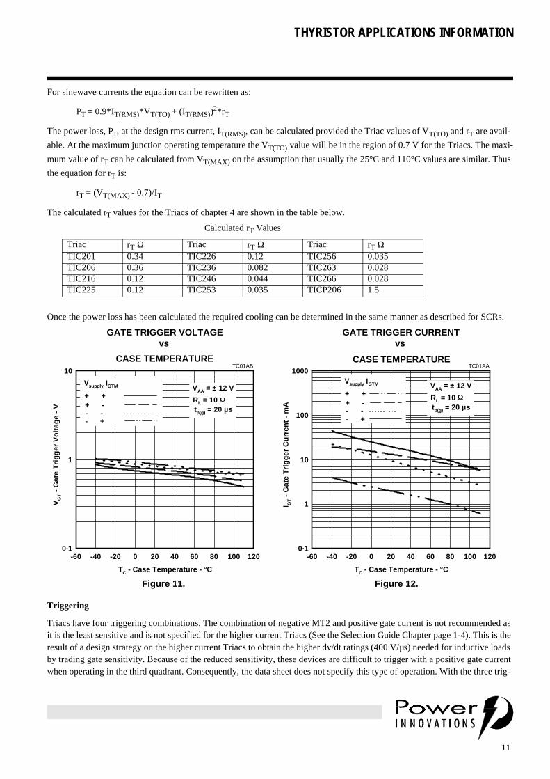
Figure 11. Figure 12.
GATE TRIGGER VOLTAGE
TC - Case Temperature - °C
-60 -40 -20 0 20 40 60 80 100 120
VG
T -
Gat
e T
rig
ger
Vo
ltag
e -
V
0·1
1
10TC01AB
CASE TEMPERATURE
vs
Vsupply IGTM
+ ++ -- -- +
VAA = ± 12 V
RL = 10 ΩΩtp(g) = 20 µs
GATE TRIGGER VOLTAGE
TC - Case Temperature - °C
-60 -40 -20 0 20 40 60 80 100 120
VG
T -
Gat
e T
rig
ger
Vo
ltag
e -
V
0·1
1
10TC01AB
CASE TEMPERATURE
vs
Vsupply IGTM
+ ++ -- -- +
VAA = ± 12 V
RL = 10 ΩΩtp(g) = 20 µs
GATE TRIGGER CURRENT
TC - Case Temperature - °C
-60 -40 -20 0 20 40 60 80 100 120
I GT -
Gat
e T
rig
ger
Cu
rren
t -
mA
0·1
1
10
100
1000TC01AA
CASE TEMPERATURE
vs
VAA = ± 12 V
RL = 10 ΩΩtp(g) = 20 µs
Vsupply IGTM
+ ++ -- -- +
THYRISTOR APPLICATIONS INFORMATION
12
gering combinations left, the design strategy is governed by the trigger source polarity. If the trigger source has the same polar-ity, then negative trigger current should be used. If the trigger source is naturally the same polarity as the MT2 voltage then this approach uses the most sensitive pair of triggering combinations and gives the lowest latching current values.
The typical temperature variation of gate trigger voltage and current are shown in Figures 11 and 12. Compared to 25°C, at 0°C the voltage has increased by 10% and the current by 30%. The data sheet maximum values at 25°C are 2 V and 50 mA. A trigger circuit designed to work down to 0°C should provide a gate current drive of 50*1.3 = 65 mA at a voltage of 2*1.1 = 2.2 V. After allowing for trigger circuit tolerances, a design giving a nominal drive of 80 mA into 2.6 V should be ade-quate.
Latching and Holding Current
Latching current is the minimum value of Main Terminal current required to maintain the Thyristor in the on-state immedi-ately after switching from the off-state to the on-state has occurred and the triggering signal has been removed. The complex nature of the Triac triggering causes the latching current to range between two to five times the holding current (See Figures 13 and 14). The Main Terminal current must be larger than the latching current when the trigger pulse ends, otherwise the Triac could switch off. There are two design solutions to this potential problem. One is to ensure the trigger pulse duration is long enough at the lowest expected operating temperature to always ensure that the latching current is reached during the trigger pulse time. The other is to have short duration multiple trigger pulses so that the device is re-triggered until latched conduction occurs. Generally the minimum trigger pulse width should not be less than 20 µs to allow for current propagation in the chip. Latching is mainly a problem for inductive loads, which will have a slow initial current rise. Snubber circuits will often be
used for voltage control with inductive loads and the discharge of this network can be used to increase the initial current value.
Commutating dv/dt, dvc/dt
This special Triac rating was discussed in the Triac theory section. Figure 15 shows the standard test circuit. The dv/dt is con-trolled by the RC snubber network and the peak on-state current is set by the inductor value. Setting the peak current will also set the commutating dic/dt (the rate of change of falling on-state current), a parameter which has a strong influence on the
dvc/dt value. Triacs of 8 A and below are tested with a specified peak current value, ITRM. Higher current Triacs are tested with
Figure 13. Figure 14.
LATCHING CURRENT
TC - Case Temperature - °C
-60 -40 -20 0 20 40 60 80 100 120
I L -
Lat
chin
g C
urr
ent
- m
A
1
10
100
1000TC01AE
CASE TEMPERATURE
vs
VAA = ± 12 V Vsupply IGTM
+ ++ -- -- +
HOLDING CURRENT
TC - Case Temperature - °C
-60 -40 -20 0 20 40 60 80 100 120
I H -
Ho
ldin
g C
urr
ent
- m
A
0·1
1
10
100
1000TC01AD
CASE TEMPERATURE
vs
Vsupply
+-
VAA = ± 12 V
IG = 0Initiating ITM = 100 mA

13
THYRISTOR APPLICATIONS INFORMATION
a specified value of dic/dt equal to 0.5*IT(RMS)/ms. With the exception of the TIC206, all the other Triacs have ITRM or IT =
1.4*IT(RMS).
The highest di/dt of a TP ms duration half sinewave will be p*ITRM/(TP) A/ms. For the lower current Triacs, the off-state volt-
age duration is specified as 0.8 ms and so the on-state current duration will be 10 - 0.8 = 9.2 ms. This gives a commutating
dic/dt of 0.34*ITRM A/ms or 0.48*IT(RMS) A/s. Thus the ITRM or 0.5*IT(RMS) specification approaches are equivalent.
APPLICATION CIRCUITS
CONTROL METHODS
Phase Control
Phase control is the technique of varying, within the cycle or half-cycle of the ac supply voltage, the instant at which the volt-age is applied to the load and current conduction begins; current conduction continues until a zero crossing is reached which switches off the Thyristor. This technique is extensively used for incandescent lamp dimming and the speed control of some dc motors. Figure 16 shows a simple phase control circuit.
Burst Firing SCRs and Triacs used in a phase control mode produce considerable radio frequency interference (r.f.i) due to the step change in current. A solution to the problem of suppression becomes more difficult and expensive as the load increases. In domestic appliances, particularly, the r.f.i. is acute and must be suppressed to comply with emc regulations. For domestic use phase con-trollable power up to 500 Watts may be acceptable. However, above this value the ratio between the phase controllable power to the total consumed power becomes significant and in addition to the expensive suppression circuit, the power factor may cause some concern.
Electric heaters and other loads with a long time constant may be controlled by passing through them a selected number of full or half cycles, See Figure 17. The current, then will be in phase with the voltage and there will be no problem of r.f.i., the
Figure 15. Commutating Test Circuit
VAC
VMT2
IMT2
DUT
SeeNote A
RG
C1
R1
IG
VAC
IMT2
VMT2
IG
ITRM
dv/dt10%
63%
L1
VDRM
50 Hz
PMC2AA
NOTE A: The gate-current pulse is furnished by a trigger circuit which presents essentially an open circuit between pulses. The pulse is timed so that the off-state-voltage duration is approximately 800 µs.

THYRISTOR APPLICATIONS INFORMATION
14
switching taking place at the point when the voltage crosses zero. Such control is called Burst Firing or Zero Voltage Switch-ing. Burst firing is not suitable for lamp dimming due to the flicker, or for Motor Speed Control and transformer input control.
SCR CIRCUITS
Half-Wave Motor Speed Control
Half-wave phase control of a universal motor allows the motor to run up to 80% of its maximum full-wave speed. Thus a use-ful speed range is obtained with only half-wave control. The universal motor generates a back emf proportional to its speed. By placing the motor in series with the control loop, drops in the back emf, caused by speed reduction, reduce the time of the next SCR triggering pulse which applies more voltage to the motor on the next cycle. This arrangement provides motor speed regulation. The basic control circuit is shown in Figure 18.
Gas Ignitor
Figure 16. Simple Phase Control Circuit
Figure 17. Burst Firing
AR210AA
Vs
DIAC
250 kΩΩ
0.2 µµF
240 V
50 Hz
LOAD
TRIAC
AR086AB
PO/3
2PO/3PO
PO/2
15
THYRISTOR APPLICATIONS INFORMATION
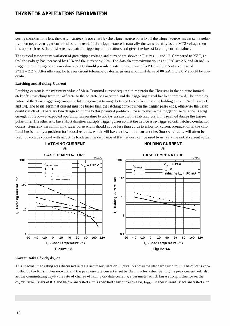
This is an example of an application that requires high current and voltage capability with relatively little long term power requirement. Typically a TO-92 TICP106 would be used as the high current switch. For time periods less than 1 ms the
TICP106 has the same silicon current capability as the TO-220 TIC106. The basic circuit is shown in Figure 19.
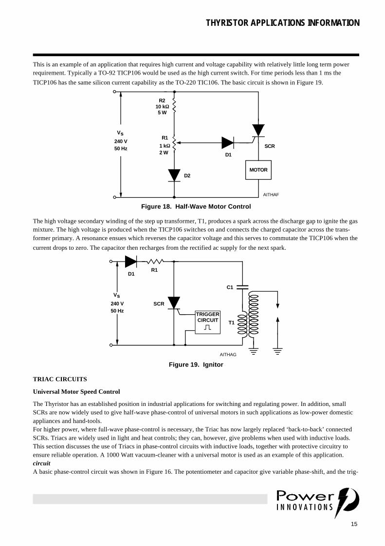
The high voltage secondary winding of the step up transformer, T1, produces a spark across the discharge gap to ignite the gas mixture. The high voltage is produced when the TICP106 switches on and connects the charged capacitor across the trans-former primary. A resonance ensues which reverses the capacitor voltage and this serves to commutate the TICP106 when the
current drops to zero. The capacitor then recharges from the rectified ac supply for the next spark.
TRIAC CIRCUITS
Universal Motor Speed Control
The Thyristor has an established position in industrial applications for switching and regulating power. In addition, small SCRs are now widely used to give half-wave phase-control of universal motors in such applications as low-power domestic appliances and hand-tools.For higher power, where full-wave phase-control is necessary, the Triac has now largely replaced ‘back-to-back’ connected SCRs. Triacs are widely used in light and heat controls; they can, however, give problems when used with inductive loads. This section discusses the use of Triacs in phase-control circuits with inductive loads, together with protective circuitry to ensure reliable operation. A 1000 Watt vacuum-cleaner with a universal motor is used as an example of this application.circuitA basic phase-control circuit was shown in Figure 16. The potentiometer and capacitor give variable phase-shift, and the trig-
Figure 18. Half-Wave Motor Control
Figure 19. Ignitor
AITHAF
Vs
MOTOR
240 V50 Hz SCR1 kΩΩ
2 W
R1
10 kΩΩ5 W
R2
D1
D2
AITHAG
C1
R1
T1
TRIGGERCIRCUIT
Vs240 V50 Hz
D1
SCR

THYRISTOR APPLICATIONS INFORMATION
16
ger diode, or diac, ensures reliable triggering of the Triac. Although control is possible from approximately 0° to 180° the cir-cuit has some drawbacks. It may be noticed, when using the circuit, that once the Triac has been turned ‘on’ at the minimum voltage, the voltage may be further reduced by increasing the potentiometer resistance. In other words, the striking voltage appears to be higher than the turning ‘off’ voltage. This hysteresis type phenomenon is attributed to the trigger diode break-down.In order to reduce the effect on hysteresis and also extend the range of control a second RC network may be added as shown in Figure 20. After the trigger diode has turned ‘on’, the partly discharged capacitor ‘C2’ is recharged by some of the energy from capacitor ‘C1’. This occurs during the time the Triac is conducting, hence the smaller hysteresis. This is a basic circuit recom-
mended for light dimmers and universal motors as mentioned earlier. The selection of components will be discussed later.
protectionTo ensure the satisfactory operation of equipment using semiconductor devices, the problem of protection must be solved. There are several points to which a designer must pay attention, i.e., the rate of rise of voltage (dv/dt), the rate of rise of cur-rent, (di/dt), voltage surges and overloads.
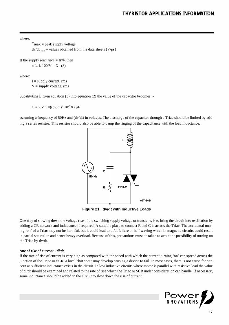
commutation and critical dv/dtWhen used with inductive loads, Triacs and SCRs are subjected to a rapid rise of voltage. If a device is not capable of with-standing such fast rises in voltages, it will lose control. The problem of dv/dt becomes important especially after commutation when the capability of a device becomes lower.From Figure 21 it can be seen the Triac will be exposed to ‘commutation dv/dt’. ‘Commutation dv/dt’ occurs when the block-ing voltage is being stressed across the device during the time it is recovering from the principle current. Malfunctioning can even occur due to fast voltage transients initiated at switch-on. This characteristic phenomenon of Triacs and SCRs is caused by capacitive coupling between gate and MT2 terminal for Triacs and gate and anode for SCR. Unwanted turn ‘on at full volt-age could bring some problems, especially when the equipment is feeding low impedance loads such as stationary motors or a bank of filament lamps. Excessive currents flowing, even for half a cycle, could blow the protective fuses or damage some of the semiconductors. The gates of the Triacs will resume control after half a cycle.
Solving and analysing the following equation :-
L(di/dt) + Ri (1/c) ƒ i.d.t = Vmax (1)
gives
(dv/dt)max = Vmax/ √LC
hence
C = V2max/L. (dv/dt)max2(2)
Figure 20. Improved Phase Control Circuit
AR210AF
Vs
LOAD
240 V50 Hz
DIAC
TRIAC
250 kΩΩ
R1
22 kΩΩR3
3.9 kΩΩR2
0.1 µµF
C10.03 µµF
C2
17
THYRISTOR APPLICATIONS INFORMATION
where:Vmax = peak supply voltagedv/dtmax = values obtained from the data sheets (V/µs)
If the supply reactance = X%, then
ωL. I. 100/V = X (3)
where:I = supply current, rmsV = supply voltage, rms
Substituting L from equation (3) into equation (2) the value of the capacitor becomes :-
C = 2.V.π.I/((dv/dt)2.102.X) µF
assuming a frequency of 50Hz and (dv/dt) in volts/µs. The discharge of the capacitor through a Triac should be limited by add-
ing a series resistor. This resistor should also be able to damp the ringing of the capacitance with the load inductance.
One way of slowing down the voltage rise of the switching supply voltage or transients is to bring the circuit into oscillation by adding a CR network and inductance if required. A suitable place to connect R and C is across the Triac. The accidental turn-ing ‘on’ of a Triac may not be harmful, but it could lead to di/dt failure or half waving which in magnetic circuits could result in partial saturation and hence heavy overload. Because of this, precautions must be taken to avoid the possibility of turning on the Triac by dv/dt.
rate of rise of current - di/dtIf the rate of rise of current is very high as compared with the speed with which the current turning ‘on’ can spread across the junction of the Triac or SCR, a local “hot spot” may develop causing a device to fail. In most cases, there is not cause for con-cern as sufficient inductance exists in the circuit. In low inductive circuits where motor is parallel with resistive load the value of di/dt should be examined and related to the rate of rise which the Triac or SCR under consideration can handle. If necessary, some inductance should be added in the circuit to slow down the rise of current.
Figure 21. dv/dt with Inductive Loads
TRIAC
C
R
L
50 Hz
AITHAH

THYRISTOR APPLICATIONS INFORMATION
18
voltage transientsDiodes and SCRs can be destroyed when subjected to excessive voltage transients, unless they incorporate avalanche charac-teristics. The Triac, being a bidirectional switch, will simply break over in one or other direction, turning ‘on’ into conduction. In spite of these self protective capabilities, the turning "on" of a Triac, even for one isolated pulse, may not be acceptable as explained earlier. An effective surge absorbing device, therefore, is necessary for reliable operation. Voltage transients can be initiated by various means such as switching transformers, inductors, from Thyristor circuits as commutation spikes, etc. The suppression of transient voltages can easily be achieved if the sources and causes of transients are known. Voltage transients generated by switching ‘off’ transformers are known to a certain extent. The energy, E, stored in the magnetic field can be
evaluated from the equation E = ½LI2 where ‘I’ is the peak magnetising current. By using a CR network as a surge absorbing
device, a simple comparison of the magnetic energy with energy to be absorbed by the capacitor used (½CV2) will give its required value. There are many surge absorbing devices on the market in the form of CR networks, VDR (voltage dependent resistors) or silicon carbide units. If the magnitude of the transient is unknown, a trial and error approach to the problem is often unavoidable
current surgesAs an example a 1000 W vacuum cleaner has been chosen for evaluation to obtain typical data for the 1000 W universal motor. Motor control was achieved with the use of double RC circuit. No excessive di/dt transients were observed but the peak start-ing surge current was significant. At low speeds, a starting surge current of up to 50 A peak was noticed with immediate return to a steady state condition. There were more serious conditions at higher speeds when the return to steady state took much longer, about 20 cycles. The first switching on peak surge current is of the same order as stall current.
snubber circuitIt is necessary to have a circuit or device which will absorb voltage spikes and eliminate dv/dt switching. The simplest and cheapest circuit for this application is a RC network connected across the Triac as shown in Figure 21. The basic function and design of the snubber was discussed in the previous paragraph. However, after selecting a suitable capacitor ‘C’, care must be taken not to damage the Triac by di/dt, as a result of ‘C’ discharging via a resistor R.
When the Triac is in the blocking state, capacitor ‘C’ is being charged. At the point of turning ‘on’, the capacitor ‘C’ is dis-
charged rapidly, with a current limited only by resistor ‘R’. Using a value of 0.1 µF for capacitor C, a resistor R value of 47 Ω
gave a di/dt of 25 A/µs. Values of 100 Ω gave 15 A/µs and 820 Ω gave a satisfactory 1 A/µs. At the point of turning ‘off’ with inductive loads, a blocking voltage is stressed across the device. If the rate of voltage rise(dv/dt) is too high, the device will turn ‘on’ again as explained previously. Using low values of resistor R was found to allow resonance and resulted in rapid voltage rises.
snubber circuit recommendationAfter selecting capacitance ‘C’ which would adequately absorb the voltage transients spikes and/or give sufficient slope in voltage blocking, the following values of series resistors have been found to give acceptable results :-
0.022 µF in series with 560 Ω
0.047 µF in series with 680 Ω
0.1 µF in series with 820 Ω
The above capacitors will cover most of the requirements ranging from small, medium to large appliances.
triac selection for 1000 W vacuum cleanerIt has been demonstrated that the decisive point in selecting Triacs for vacuum cleaners is the surge current capability and di/dt rating. Surges of 50 A peak, decreasing after 20 cycles to a steady value, can be expected. However, a generous safety margin is essential, since other factors such as commutator wear, cleanliness and lubrication of bearings, and behaviour at low temper-
19
THYRISTOR APPLICATIONS INFORMATION
atures, could all result in higher current surges.
The Triac Type TIC236M (12 A, 600 V) is therefore recommended for the application. Without a snubber network, it can with-stand a typical dv/dt of 2 V/µs. The use of a centre gate gives the unusually high di/dt of 200 A/µs, and this allows the use of a generous snubber network to further increase dv/dt capability. With the particular motor used, a snubber circuit consisting of
0.047 µF in series with 680 Ω was found satisfactory. The basic circuit shown in Figure 20 was used, with these components :-
R1 - 250 kΩR2 - 22 kΩ
R3 - 3.3 kΩC1 - 0.1 µFC2 - 0.033 µF
conclusionThis section shows the importance of current ratings (steady state, surge and di/dt) when selecting Triacs to control universal motors. Similar considerations apply with other loads, such as filament lamps, where high surge current can also be expected.dv/dt with industrial loads, is usually less of a problem, since snubber networks can be used to improve capability. However, care must be taken that di/dt ratings are not exceeded. Whereas occasional false triggering as a result of excessive dv/dt is sel-dom destructive to the Triac, excessive di/dt can cause degradation and eventual failure.
In view of the many variables present in loads which Triacs are required to control, it is important to evaluate performance thoroughly and provide a generous safety margin to comprehend normal and faulty conditions.
Lamp Dimmers
The circuit of Figure 20 is suitable for incandescent lamp dimming and this section is concerned with Triac selection. With normal lamps the "cold" surge current is typically eight times the running current. Halogen lamps double this value and surges of fifteen times running occur when the lamp is cold. When a lamp fails, the filament can form a progressive short which, in bad cases, can blow the circuit fuses. If it is desirable that the Triac does not fail due to a high surge lamp failure, the Triac surge current rating should be selected to be at least one hundred times the lamp running current.
Triac Switching using Optically Coupled Isolators
Low power optocoupled Triacs simplify the interfacing between low voltage electronics and power Triacs. Three circuits are shown in Figure 22, which cover resistive loads and inductive loads with low and high sensitivity Triacs.

THYRISTOR APPLICATIONS INFORMATION
20
References
1. "GE Silicon Controlled Rectifier Manual", Second Edition
2. "Semiconductor and Components Data Book 5 - Diodes, Rectifiers, Optoelectronics and microwave", Texas Instruments, 1969
The information presented in this book is based on the following "B" series of Application Reports written by Jurek Budek
Figure 22. Optocoupled Triac Drive
AITHAI
RESISTIVE LOAD
TIL3020 - TIL3023 RL
i 180 ΩΩ
230 V50 Hz
INDUCTIVE LOAD WITH SENSITIVE GATE TRIAC, IGT < 15 mA
TIL3020 - TIL3023 ZL
230 V50 Hz
i 180 ΩΩ 2.4 kΩΩ
0.1 µF
INDUCTIVE LOAD WITH NONSENSITIVE-GATE TRIAC, 15 mA < IGT < 50 mA
TIL3020 - TIL3023 ZL
230 V50 Hz
i 180 ΩΩ 1.2 kΩΩ
0.2 µF
21
THYRISTOR APPLICATIONS INFORMATION
"Triacs-Theory and General Applications", B61, July 1969
"Triacs with Resistive and Inductive Loads", B70, Revised November 1970
"Solid-State Switching using Triacs and Thyristors", B75, October 1969
"Burst Firing Techniques using Triacs", B86, March 1970
"Power Control with Triacs", B130
"Electric Cooker Control", B172
"Triac Speed Control of Universal Motors", B210