
THVD1505 Bus-Polarity Correcting RS-485 Transceiver With ...
32
A B D DE R RE D R 5V 1k 1k A B D DE R RE POLCOR D R A B D DE R POLCOR D R RE A B D DE R POLCOR D R RE Master THVD1500 Slave THVD1505 Slave THVD1505 Slave THVD1505 Cross-wire fault 0 Copyright © 2018, Texas Instruments Incorporated Product Folder Order Now Technical Documents Tools & Software Support & Community An IMPORTANT NOTICE at the end of this data sheet addresses availability, warranty, changes, use in safety-critical applications, intellectual property matters and other important disclaimers. PRODUCTION DATA. THVD1505 SLLSF68 – SEPTEMBER 2019 THVD1505 Bus-Polarity Correcting RS-485 Transceiver With IEC-ESD Protection 1 1 Features 1• Meets or exceeds the requirements of the TIA/EIA-485A standard and the State Grid Corporation of China (SGCC) Part 11 Serial Communication Protocol RS-485 standard • 4.5-V to 5.5-V supply voltage • Half-duplex RS-422 / RS-485 • Bus polarity correction within 45 ms • Works with or without fail-safe biasing resistors • Data rate: up to 1 Mbps • Bus I/O protection: – ±16-kV HBM ESD – ±8-kV IEC 61000-4-2 contact discharge – ±8-kV IEC 61000-4-2 air-gap discharge – ±2-kV IEC 61000-4-4 fast transient burst • Open, short, and idle bus fail-safe • Large receiver hysteresis for noise rejection: 120 mV • Up to 256 nodes on a bus (1/8 unit load) • Extended ambient temperature range: -40°C to 125°C • Low power consumption – Standby supply current: < 1 μA – Operational supply current: < 1.1 mA • Glitch-free power-up / down for hot plug-in capability 2 Applications • Electricity meters • HVAC systems • Inverters • Video surveillance 3 Description The THVD1505 is a low-power RS-485 transceiver with automatic bus-polarity correction and transient protection. Upon hot plug-in, the device detects and corrects the bus polarity within the first 45 ms of bus idling. The bus pins are robust to electrostatic discharge (ESD) events, with high levels of protection to human-body model (HBM), IEC 61000-4-2 contact discharge and air-gap discharge specifications. The device combines a differential driver and a differential receiver, which operate together from a single 5-V power supply. The driver differential outputs and the receiver differential inputs are connected internally to form a bus port suitable for half-duplex (two-wire bus) communication. The device features a wide common-mode voltage range making the device suitable for multi-point applications over long cable runs. The THVD1505 is available in an SOIC-8 package, and is characterized for free-air temperatures from –40°C to 125°C. Device Information (1) PART NUMBER PACKAGE BODY SIZE (NOM) THVD1505 SOIC (8) 4.90 mm × 3.91 mm (1) For all available packages, see the orderable addendum at the end of the datasheet. Typical Network Application With Polarity Correction (POLCOR)
Transcript of THVD1505 Bus-Polarity Correcting RS-485 Transceiver With ...

A
B
D
DE
R
RE
D
R
5V
1k
1k
A
B
D
DE
R
RE
PO
LC
OR
D
R
A B
DDER
POLCOR
DR
RE
A B
DDER
POLCOR
DR
RE
Master
THVD1500
Slave
THVD1505
Slave
THVD1505
Slave
THVD1505
Cross-wire
fault 0
Copyright © 2018, Texas Instruments Incorporated
Product
Folder
Order
Now
Technical
Documents
Tools &
Software
Support &Community
An IMPORTANT NOTICE at the end of this data sheet addresses availability, warranty, changes, use in safety-critical applications,intellectual property matters and other important disclaimers. PRODUCTION DATA.
THVD1505SLLSF68 –SEPTEMBER 2019
THVD1505 Bus-Polarity Correcting RS-485 Transceiver With IEC-ESD Protection
1
1 Features1• Meets or exceeds the requirements of the
TIA/EIA-485A standard and the State GridCorporation of China (SGCC) Part 11 SerialCommunication Protocol RS-485 standard
• 4.5-V to 5.5-V supply voltage• Half-duplex RS-422 / RS-485• Bus polarity correction within 45 ms• Works with or without fail-safe biasing resistors• Data rate: up to 1 Mbps• Bus I/O protection:
– ±16-kV HBM ESD– ±8-kV IEC 61000-4-2 contact discharge– ±8-kV IEC 61000-4-2 air-gap discharge– ±2-kV IEC 61000-4-4 fast transient burst
• Open, short, and idle bus fail-safe• Large receiver hysteresis
for noise rejection: 120 mV• Up to 256 nodes on a bus (1/8 unit load)• Extended ambient temperature
range: -40°C to 125°C• Low power consumption
– Standby supply current: < 1 µA– Operational supply current: < 1.1 mA
• Glitch-free power-up / down for hot plug-incapability
2 Applications• Electricity meters• HVAC systems• Inverters• Video surveillance
3 DescriptionThe THVD1505 is a low-power RS-485 transceiverwith automatic bus-polarity correction and transientprotection. Upon hot plug-in, the device detects andcorrects the bus polarity within the first 45 ms of busidling. The bus pins are robust to electrostaticdischarge (ESD) events, with high levels of protectionto human-body model (HBM), IEC 61000-4-2 contactdischarge and air-gap discharge specifications.
The device combines a differential driver and adifferential receiver, which operate together from asingle 5-V power supply. The driver differentialoutputs and the receiver differential inputs areconnected internally to form a bus port suitable forhalf-duplex (two-wire bus) communication. Thedevice features a wide common-mode voltage rangemaking the device suitable for multi-point applicationsover long cable runs. The THVD1505 is available inan SOIC-8 package, and is characterized for free-airtemperatures from –40°C to 125°C.
Device Information(1)
PART NUMBER PACKAGE BODY SIZE (NOM)THVD1505 SOIC (8) 4.90 mm × 3.91 mm
(1) For all available packages, see the orderable addendum atthe end of the datasheet.
Typical Network Application With Polarity Correction (POLCOR)

2
THVD1505SLLSF68 –SEPTEMBER 2019 www.ti.com
Product Folder Links: THVD1505
Submit Documentation Feedback Copyright © 2019, Texas Instruments Incorporated
Table of Contents1 Features .................................................................. 12 Applications ........................................................... 13 Description ............................................................. 14 Revision History..................................................... 25 Pin Configuration and Functions ......................... 36 Specifications......................................................... 3
6.1 Absolute Maximum Ratings ...................................... 36.2 ESD Ratings.............................................................. 36.3 ESD Ratings [IEC] .................................................... 46.4 Recommended Operating Conditions....................... 46.5 Thermal Information .................................................. 46.6 Electrical Characteristics........................................... 56.7 Power Dissipation Characteristics ............................ 66.8 Switching Characteristics .......................................... 66.9 Typical Characteristics .............................................. 7
7 Parameter Measurement Information .................. 87.1 Driver......................................................................... 87.2 Receiver .................................................................... 9
8 Detailed Description ............................................ 11
8.1 Overview ................................................................ 118.2 Functional Block Diagram ....................................... 118.3 Feature Description................................................. 118.4 Device Functional Modes........................................ 15
9 Application and Implementation ........................ 169.1 Application Information............................................ 169.2 Typical Application ................................................. 21
10 Power Supply Recommendations ..................... 2311 Layout................................................................... 24
11.1 Layout Guidelines ................................................. 2411.2 Layout Example ................................................... 24
12 Device and Documentation Support ................. 2512.1 Device Support...................................................... 2512.2 Receiving Notification of Documentation Updates 2512.3 Community Resources.......................................... 2512.4 Trademarks ........................................................... 2512.5 Electrostatic Discharge Caution............................ 2512.6 Glossary ................................................................ 25
13 Mechanical, Packaging, and OrderableInformation ........................................................... 25
4 Revision HistoryNOTE: Page numbers for previous revisions may differ from page numbers in the current version.
DATE REVISION NOTESSeptember 2019 * Initial release.

1R 8 VCC
2RE 7 B
3DE 6 A
4D 5 GND
Not to scale
3
THVD1505www.ti.com SLLSF68 –SEPTEMBER 2019
Product Folder Links: THVD1505
Submit Documentation FeedbackCopyright © 2019, Texas Instruments Incorporated
5 Pin Configuration and Functions
D Package8-Pin SOICTop View
Pin FunctionsPIN
I/O DESCRIPTIONNAME NO.
A 6 Businput/output Driver output or receiver input (complementary to B)
B 7 Businput/output Driver output or receiver input (complementary to A)
D 4 Digital input Driver data input (internal 5-MΩ pull-up)DE 3 Digital input Driver enable, active high (internal 5-MΩ pull-down)
GND 5 Ground Device groundR 1 Digital output Receive data output
RE 2 Digital input Receiver enable, active low (internal 5-MΩ pull-up)VCC 8 Supply 4.5-V to 5.5-V supply
(1) Stresses beyond those listed under Absolute Maximum Ratings may cause permanent damage to the device. These are stress ratingsonly and functional operation of the device at these or any other conditionsbeyond those indicated under Recommended OperatingConditions is not implied. Exposure to absolute-maximum-rated conditions forextended periods may affect device reliability.
6 Specifications
6.1 Absolute Maximum Ratingsover operating free-air temperature range (unless otherwise noted) (1)
MIN MAX UNIT
VCC Supply voltage –0.5 7 V
VL Input voltage at any logic pin (D, DE or RE) –0.3 5.7 V
VA, VB Voltage at A or B inputs, as differential or common-mode with respect to GND –18 18 V
IO Receiver output current –24 24 mA
TJ Junction temperature 170 °C
TSTG Storage temperature –65 150 °C
(1) JEDEC document JEP155 states that 500-V HBM allows safe manufacturing with a standard ESD control process.(2) JEDEC document JEP157 states that 250-V CDM allows safe manufacturing with a standard ESD control process.
6.2 ESD RatingsVALUE UNIT
V(ESD) Electrostatic discharge
Human body model (HBM), per ANSI/ESDA/JEDEC JS-001 (1) Bus terminals and GND ±16,000
VAll other pins ±4,000
Charged-device model (CDM), per JEDEC specification JESD22-C101 (2) ±1,500
Machine model (MM), per JEDEC JESD22-A115-A ±400

4
THVD1505SLLSF68 –SEPTEMBER 2019 www.ti.com
Product Folder Links: THVD1505
Submit Documentation Feedback Copyright © 2019, Texas Instruments Incorporated
6.3 ESD Ratings [IEC]VALUE UNIT
V(ESD) Electrostatic discharge
IEC 61000-4-2 ESD contact discharge, bus terminals and GND ±8,000
VIEC 61000-4-2 ESD air-gap discharge, bus terminals and GND ±8,000
IEC 61000-4-4 EFT fast transient, bus terminals and GND ±2,000
(1) The algebraic convention in which the least positive (most negative) limit is designated as minimum is used in this datasheet.(2) Operation is specified for internal (junction) temperatures upto 150°C. Self-heating due to internal power dissipation should be
considered for each application. Maximum junction temperature is internally limited by the thermal shutdown (TSD) circuit which disablesthe device when the junction temperature reaches 170°C.
6.4 Recommended Operating ConditionsMIN NOM MAX UNIT
VCC Supply voltage 4.5 5 5.5 V
VID Differential input voltage –12 12 V
VI Input voltage at any bus terminal (1) –7 12 V
VIH High-level input voltage (driver, driver-enable, and receiver-enable inputs) 2 VCC V
VIL Low-level input voltage (driver, driver-enable, and receiver-enable inputs) 0 0.8 V
IO Output currentDriver –60 60
mAReceiver –8 8
RL Differential load resistance 54 60 Ω
1/tUI Signaling rate 0.3 1000 kbps
TJ Junction temperature –40 150 °C
TA(2) Operating ambient temperature (see Thermal Information for additional information) –40 125 °C
(1) For more information about traditional and new thermalmetrics, see the Semiconductor and ICPackage Thermal Metrics applicationreport.
6.5 Thermal Information
THERMAL METRIC (1)
THVD1505
UNITD (SOIC)
8 PINS
RθJA Junction-to-ambient thermal resistance 125.3 °C/W
RθJC(top) Junction-to-case (top) thermal resistance 67.6 °C/W
RθJB Junction-to-board thermal resistance 68.6 °C/W
ψJT Junction-to-top characterization parameter 20.4 °C/W
ψJB Junction-to-board characterization parameter 67.8 °C/W

5
THVD1505www.ti.com SLLSF68 –SEPTEMBER 2019
Product Folder Links: THVD1505
Submit Documentation FeedbackCopyright © 2019, Texas Instruments Incorporated
(1) Under any specific conditions, VIT+ is specified to be at least VHYS higher thanVIT–.
6.6 Electrical Characteristicsover operating free-air temperature range (unless otherwise noted)
PARAMETER TEST CONDITIONS MIN TYP MAX UNIT
Driver
│VOD│Driver differential-output voltagemagnitude
Vtest from –7 to +12 V See Figure 7 1.5 2.5
VRL = 54 Ω (RS-485), CL = 50 pFSee Figure 8
1.5 2.5
RL = 100 Ω (RS-422), CL = 50 pF 2 3
Δ│VOD│Change in magnitude of driverdifferential-output voltage RL = 54 Ω, CL = 50 pF See Figure 8 –50 50 mV
VOC(SS)Steady-state common-modeoutput voltage
RL = 54 Ω, CL = 50 pF See Figure 8
1 VCC / 2 3 V
ΔVOCChange in differential drivercommon-mode output voltage –50 50 mV
VOC(PP)Peak-to-peak driver common-mode output voltage 250 mV
│IOS│ Driver short-circuit output current DE = VCC, -7 V ≤ [VA or VB] ≤ 12 V, or A pin shorted to Bpin 150 mA
COD Differential output capacitance 8 pF
Receiver
II Bus input current (driver disabled) DE = 0 V, VCC = 0 V or 5.5 VVI = 12 V 75 110
µAVI = –7 V –90 –70
RA, RB Bus input impedance VA = -7 V, VB = 12 V and VA = 12V, VB = -7 V See Figure 12 96 kΩ
VIT+Positive-going receiverdifferential-input voltage threshold 60 100 mV
VIT–Negative-going receiverdifferential-input voltage threshold –100 –60 mV
VHYS(1) Receiver differential-input voltage
threshold hysteresis (VIT+ – VIT– ) 40 120 mV
VOH Receiver high-level output voltage IOH = –8 mA 4 VCC – 0.3 V
VOL Receiver low-level output voltage IOL = 8 mA 0.2 0.4 V
IOZReceiver high-impedance outputcurrent VO = 0 V or VCC, RE = VCC –1 1 µA
IOSRReceiver output short-circuitcurrent RE = 0, DE = 0 See Figure 13 95 mA
Logic
IIN Input current (D, DE, RE) –2 2 µA
Supply
ICC Supply current (quiescent)
Driver and receiver enabled DE = VCC, RE = 0,no load 820 1100
µADriver enabled, receiver disabled DE = VCC, RE =
VCC, no load 520 660
Driver disabled, receiver enabled DE = 0, RE = 0, noload 520 660
Driver and receiver disabled DE = 0, RE = VCC,no load 0.03 1

6
THVD1505SLLSF68 –SEPTEMBER 2019 www.ti.com
Product Folder Links: THVD1505
Submit Documentation Feedback Copyright © 2019, Texas Instruments Incorporated
6.7 Power Dissipation CharacteristicsPARAMETER TEST CONDITIONS VALUE UNIT
PD
Power dissipation, driver andreceiver enabled, VCC = 5.5 V, TA =125°C, 50% duty cycle square-wavesignal at maximum signaling rate
Unterminated RL = 300 Ω, CL = 50 pF 120
mWRS-422 load RL = 100 Ω, CL = 50 pF 160
RS-485 load RL = 54 Ω, CL = 50 pF 200
6.8 Switching Characteristicsover operating free-air temperature range (unless otherwise noted)
PARAMETER TEST CONDITIONS MIN TYP MAX UNIT
Driver
tr, tf Driver differential output rise and fall times See Figure 9 100 115 300 ns
tPHL, tPLH Driver propagation delay See Figure 9 90 350 ns
tSK(P) Driver pulse skew, |tPHL – tPLH| See Figure 9 25 40 ns
tPHZ, tPLZ Driver disable time See Figure 10 andFigure 11 70 160 ns
tPHZ, tPLZ Driver enable timeReceiver enabled See Figure 10 and
Figure 11 220 400 ns
Receiver disabled See Figure 10 andFigure 11 1.5 3 µs
Receiver
tr, tf Receiver output rise and fall times See Figure 14 6 30 ns
tPHL, tPLH Receiver propagation delay time See Figure 14 80 120 ns
tSK(P) Receiver pulse skew, |tPHL – tPLH| See Figure 14 2 7 ns
tPHZ, tPLZ Receiver disable time See Figure 15 15 30 ns
tPZL(1),tPZH(1)tPZL(2),tPZH(2)
Receiver enable time
Driver enabled See Figure 15 180 370 ns
Driver disabled See Figure 16 1 5 µs
tFS Bus fail-safe time Driver disabled See Figure 17 25 35 45 ms
Temperature (0C)
Dri
ve
r P
rop
ag
atio
n D
ela
y (
ns)
-40 -20 0 20 40 60 80 100 120 14086
86.5
87
87.5
88
88.5
89
89.5
90
90.5
91
D_00
TPLH
TPHL
Signaling Rate (kbps)
Supply
Curr
ent (m
A)
0 100 200 300 400 500 600 700 800 900 100044.9
44.95
45
45.05
45.1
45.15
45.2
45.25
45.3
45.35
D_00
Supply Voltage (V)
Dri
ver
Outp
ut C
urr
ent (m
A)
0 0.5 1 1.5 2 2.5 3 3.5 4 4.5 5 5.5 6 6.5 70
5
10
15
20
25
30
35
40
45
50
55
60
65
D_00Temperature (0C)
Dri
ve
r R
ise
an
d F
all
Tim
es (
ns)
-40 -20 0 20 40 60 80 100 120 140114
116
118
120
122
124
126
128
130
D_00
Rise timeFall time
Driver Output Current (mA)
Dri
ver
Outp
ut V
oltag
e (
V)
0 5 10 15 20 25 30 35 40 45 50 55 60 65 70 750.3
0.6
0.9
1.2
1.5
1.8
2.1
2.4
2.7
3
3.3
3.6
3.9
4.2
4.5
4.8
D_00
VOL
VOH
Driver Output Current (mA)
Dri
ve
r D
iffe
ren
tia
l O
utp
ut
Vo
lta
ge
(V
)
0 5 10 15 20 25 30 35 40 45 50 55 60 65 70 75-0.6
0
0.6
1.2
1.8
2.4
3
3.6
4.2
D_00
7
THVD1505www.ti.com SLLSF68 –SEPTEMBER 2019
Product Folder Links: THVD1505
Submit Documentation FeedbackCopyright © 2019, Texas Instruments Incorporated
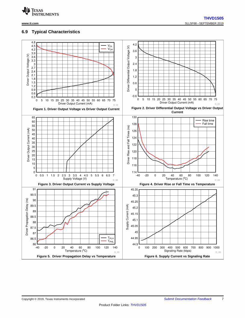
6.9 Typical Characteristics
Figure 1. Driver Output Voltage vs Driver Output Current Figure 2. Driver Differential Output Voltage vs Driver OutputCurrent
Figure 3. Driver Output Current vs Supply Voltage Figure 4. Driver Rise or Fall Time vs Temperature
Figure 5. Driver Propagation Delay vs Temperature Figure 6. Supply Current vs Signaling Rate
VO
VI
tPZL tPLZ
50%
50%
5V
§�5V
0V
VOL10%Input
Generator
A
B
VOD
RL= 110 �
VI50�
DECL=
50 pF
S1
5V
VO
VI
tPZH
tPHZ
50%
50%
5V
§�0V
0V
VOH90%Input
Generator
A
B
VOD
RL=
110 �
VI50�
DECL=
50 pF
S1
VOD
VI
tPLH tPHL
tr tf
90%
50%
10%
50%
5V
§�2V
§�-2V
0V
Input
Generator
A
B
Vcc
VODD 54 �
VI50�
DE
CL=
50 pF
A
B
VOC
VOC(PP)ûVOC(SS)
VA
VB0V or 5 V
A
B
VODD
RL/2
RL/2
CLVOC
0V or 5 V
A
B
DE
Vcc
Vtest
VOD
D
375 �
60 �
375 �
8
THVD1505SLLSF68 –SEPTEMBER 2019 www.ti.com
Product Folder Links: THVD1505
Submit Documentation Feedback Copyright © 2019, Texas Instruments Incorporated
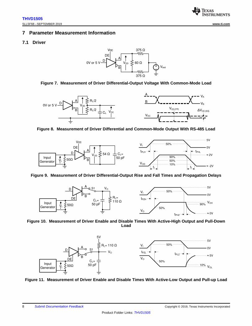
7 Parameter Measurement Information
7.1 Driver
Figure 7. Measurement of Driver Differential-Output Voltage With Common-Mode Load
Figure 8. Measurement of Driver Differential and Common-Mode Output With RS-485 Load
Figure 9. Measurement of Driver Differential-Output Rise and Fall Times and Propagation Delays
Figure 10. Measurement of Driver Enable and Disable Times With Active-High Output and Pull-DownLoad
Figure 11. Measurement of Driver Enable and Disable Times With Active-Low Output and Pull-up Load

VO
VI
tPHZ
50%
50%
5V
§�0V
0V
VOH90%
50%10%
VOL
VCC
tPLZtPZL(1)
VO
tPZH(1)D at 5V
S1 to GND
D at 0V
S1 to VCC
Input
Generator
VO
VI50�
A
B
R
CL= 15 pFRE
0V or 5 V
DE
Vcc
D
Vcc
1 k�S1
VOD
VI
tPLH tPHL
tr tf
90%
50%
10%
50%
5V
VOH
VOL
0V
Input
Generator
VO
VI50�
RE
A
B
R
1.5V
0V
CL= 15 pF
RE
DE
DI
R
VCC
A
B
GND
VCC
A
RE
DE
DI
R
VCC
A
B
GND
VCC
=
VA
VB
VX
Source meter to apply
VA/VB and measure IA/IB
IA
IB
9
THVD1505www.ti.com SLLSF68 –SEPTEMBER 2019
Product Folder Links: THVD1505
Submit Documentation FeedbackCopyright © 2019, Texas Instruments Incorporated
7.2 Receiver
Figure 12. Measurement of Bus Impedance
Figure 13. Measurement of Receiver Output Short Circuit Current
Figure 14. Measurement of Receiver Output Rise and Fall Times and Propagation Delays
Figure 15. Measurement of Receiver Enable and Disable Times With Driver Enabled

VI
2.2V
Input
Generator
VO
VI50�
RE
A
B
R
2.5V
0V
10 k�
50%
tFS
VO
VCC
(DE = Low)
2.8V
VO
VI
50%
5V
§�0V
0V
VOH
50%
VOL
VCC
tPZL(2)
VO
tPZH(2)
A at 1.5V
B at 0V
S1 to GND
A at 0V
B at 1.5V
S1 to VCC
50%
Input
Generator
VO
VI50�
A
B
R
CL= 15 pFRE
0V or 1.5 V
Vcc
1 k�S1
1.5 V or 0 V
10
THVD1505SLLSF68 –SEPTEMBER 2019 www.ti.com
Product Folder Links: THVD1505
Submit Documentation Feedback Copyright © 2019, Texas Instruments Incorporated
Receiver (continued)
Figure 16. Measurement of Receiver Enable Times With Driver Disabled
Figure 17. Measurement of Receiver Polarity-Correction Time With Driver Disabled

A
B
D
DE
R
PO
LC
OR
RE
Vcc
GND
A
B
D
DE
R
RE
VS-Master
RFS
RFS
RT
(opt.)
VSM
GND
Vcc
VS-Slave
RxD
TxD
DIR
MCU
DGND
Vdd
VS-Slave
RxD
TxD
DIR
MCU
DGND
Vdd
VS-Master Slave
node
Master
node
RT
(opt.)
Vcc
GND
B
A
D
DE
R
RE
PO
LC
OR
Copyright © 2018, Texas Instruments Incorporated
11
THVD1505www.ti.com SLLSF68 –SEPTEMBER 2019
Product Folder Links: THVD1505
Submit Documentation FeedbackCopyright © 2019, Texas Instruments Incorporated
8 Detailed Description
8.1 OverviewThe THVD1505 device is a half-duplex RS-485 transceiver suitable for data transmission at rates up to 1 Mbpsover controlled-impedance transmission media (such as twisted-pair cabling). The device features a high level ofinternal transient protection, making it able to withstand ESD strikes up to ±8 kV (per IEC 61000-4-2) and EFTtransients up to ±2 kV (per IEC 61000-4-4) without incurring damage. Up to 256 units of THVD1500 and/orTHVD1505 may share a common RS-485 bus due to the devices' low bus input currents. THVD1505 featuresautomatic polarity correction, which detects bus mis-wiring and swaps A and B.
8.2 Functional Block Diagram
8.3 Feature Description
8.3.1 Bus Polarity CorrectionTHVD1505 automatically corrects a wrong bus-signal polarity caused by a mis-wire fault. In order to detect thebus polarity, the following conditions must be met.• A slave node must enable the receiver (RE = low). Driver can be in either enabled or disabled state• A and B signals should be static for longer than fail-safe time (tFS)• The absolute value of the differential voltage at the receiver input should be greater than the receiver
thresholds (|VIT+| or |VIT-|)
The receiver input voltage can be defined either by using passive fail-safe resistors or by the master nodeactively driving the bus.
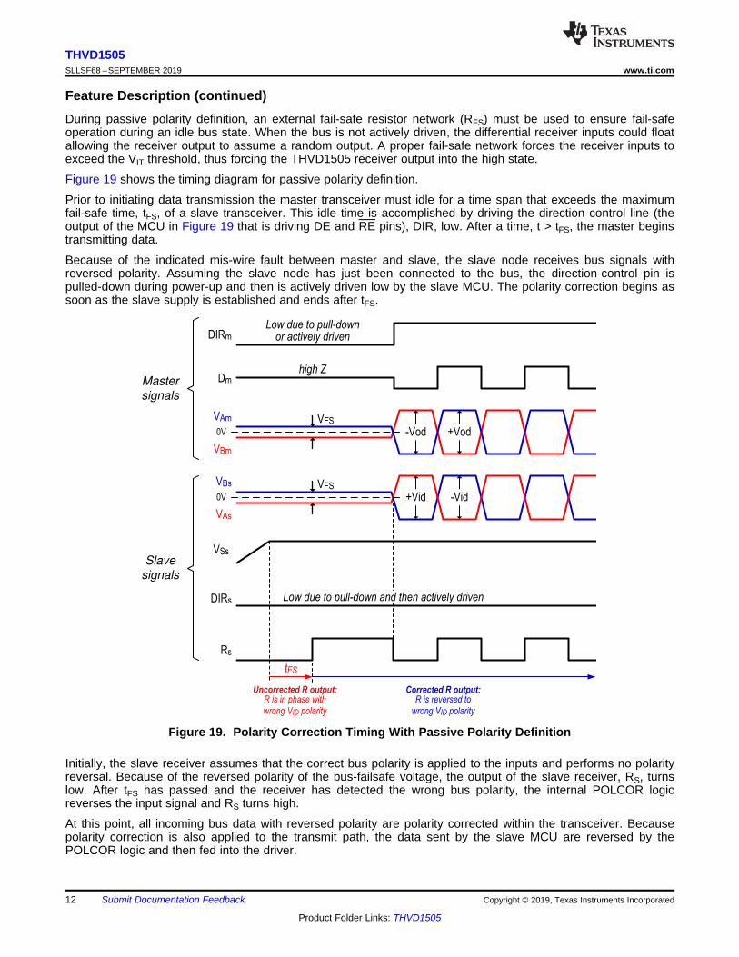
8.3.1.1 Passive Polarity Definition Using Fail-Safe Biasing NetworkFigure 18 shows a simple point-to-point data link between a master node and a slave node with mis-wire fault.
Figure 18. Passive Polarity Definition
-Vod +Vod
Dm
VAm
VBm
DIRm
high Z
-Vid+Vid
tFS
Rs
VAs
VBs
Uncorrected R output:R is in phase with
wrong VID polarity
Corrected R output:R is reversed to
wrong VID polarity
DIRs
Low due to pull-downor actively driven
VSs
Low due to pull-down and then actively driven
Master
signals
Slave
signals
VFS
VFS
0V
0V
12
THVD1505SLLSF68 –SEPTEMBER 2019 www.ti.com
Product Folder Links: THVD1505
Submit Documentation Feedback Copyright © 2019, Texas Instruments Incorporated
Feature Description (continued)During passive polarity definition, an external fail-safe resistor network (RFS) must be used to ensure fail-safeoperation during an idle bus state. When the bus is not actively driven, the differential receiver inputs could floatallowing the receiver output to assume a random output. A proper fail-safe network forces the receiver inputs toexceed the VIT threshold, thus forcing the THVD1505 receiver output into the high state.
Figure 19 shows the timing diagram for passive polarity definition.
Prior to initiating data transmission the master transceiver must idle for a time span that exceeds the maximumfail-safe time, tFS, of a slave transceiver. This idle time is accomplished by driving the direction control line (theoutput of the MCU in Figure 19 that is driving DE and RE pins), DIR, low. After a time, t > tFS, the master beginstransmitting data.
Because of the indicated mis-wire fault between master and slave, the slave node receives bus signals withreversed polarity. Assuming the slave node has just been connected to the bus, the direction-control pin ispulled-down during power-up and then is actively driven low by the slave MCU. The polarity correction begins assoon as the slave supply is established and ends after tFS.
Figure 19. Polarity Correction Timing With Passive Polarity Definition
Initially, the slave receiver assumes that the correct bus polarity is applied to the inputs and performs no polarityreversal. Because of the reversed polarity of the bus-failsafe voltage, the output of the slave receiver, RS, turnslow. After tFS has passed and the receiver has detected the wrong bus polarity, the internal POLCOR logicreverses the input signal and RS turns high.
At this point, all incoming bus data with reversed polarity are polarity corrected within the transceiver. Becausepolarity correction is also applied to the transmit path, the data sent by the slave MCU are reversed by thePOLCOR logic and then fed into the driver.
A
B
D
DE
R
PO
LC
OR
RE
Vcc
GND
A
B
D
DE
R
RE
VS-Master
RT
GND
Vcc
VS-Slave
RxD
TxD
DIR
MCU
DGND
Vdd
VS-Slave
RxD
TxD
DIR
MCU
DGND
Vdd
VS-MasterSlave
node
Master
node
RT
13
THVD1505www.ti.com SLLSF68 –SEPTEMBER 2019
Product Folder Links: THVD1505
Submit Documentation FeedbackCopyright © 2019, Texas Instruments Incorporated
Feature Description (continued)The reversed data from the slave MCU are reversed again by the mis-wire fault in the bus, and the correct buspolarity is reestablished at the master end.
THVD1505 retains the state of the polarity logic as long as VCC is present to the device. However, the devicePOLCOR logic powers up in the default no polarity reversal mode at each device power up. POLCOR logicremains active as long as VCC is applied to the device.
NOTEData string durations of consecutive 0s or 1s exceeding the minimum tFS can accidentlytrigger a wrong polarity correction and must be avoided.
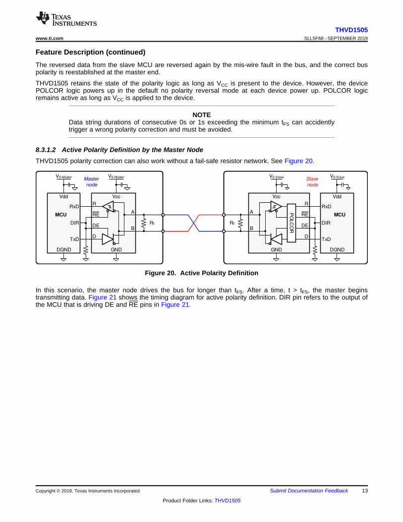
8.3.1.2 Active Polarity Definition by the Master NodeTHVD1505 polarity correction can also work without a fail-safe resistor network. See Figure 20.
Figure 20. Active Polarity Definition
In this scenario, the master node drives the bus for longer than tFS. After a time, t > tFS, the master beginstransmitting data. Figure 21 shows the timing diagram for active polarity definition. DIR pin refers to the output ofthe MCU that is driving DE and RE pins in Figure 21.

-VOD +VOD
Dm
VAm
VBm
DIRm
tFS
Rs
VAs
VBs
Uncorrected R output :R is in phase with
wrong VID polarity
Corrected R output :R is reversed to
wrong VID polarity
DIRs
Driven high
VSs
Low due to pull-down and then actively driven
Master
signals
Slave
signals
0V
0V
Driven high
VFS
+V ID -VIDVFS
14
THVD1505SLLSF68 –SEPTEMBER 2019 www.ti.com
Product Folder Links: THVD1505
Submit Documentation Feedback Copyright © 2019, Texas Instruments Incorporated
Feature Description (continued)
Figure 21. Polarity Correction Timing With Active Polarity Definition
POLCOR logic behavior with active polarity definition is identical to the POLCOR logic behavior with passivepolarity definition.

15
THVD1505www.ti.com SLLSF68 –SEPTEMBER 2019
Product Folder Links: THVD1505
Submit Documentation FeedbackCopyright © 2019, Texas Instruments Incorporated
8.4 Device Functional Modes
Table 1. Driver Pin FunctionsINPUT ENABLE OUTPUTS
DESCRIPTIOND DE A B
NORMAL MODE
H H H L Actively drives bus high
L H L H Actively drives bus low
X L Z Z Driver disabled
X OPEN Z Z Driver disabled by default
OPEN H H L Actively drives bus high
POLARITY-CORRECTING MODE
H H L H Actively drives bus low
L H H L Actively drives bus high
X L Z Z Driver disabled
X OPEN Z Z Driver disabled by default
OPEN H L H Actively drives bus low
Table 2. Receiver Pin FunctionsDIFFERENTIAL
INPUT ENABLE OUTPUTDESCRIPTION
VID = VA – VB RE DE R
VID > VIT+ L X H Receive valid bus high
VIT- > VID L X L during tFSH after tFS
Receive valid bus low if lasting for less than tFS, polarity correcting if lasting formore than tFS
X H X Z Receiver disabled
X OPEN X Z Receiver disabled
Open, short or VIT+ >VID > VIT-
L X H after tFS Receiver fail-safe high

Vcc
GND
B
A
D
DE
R
RE
PO
LC
OR
a) Independent driver and receiver enable signals
b) Combined enable signals for use as directional control pin
c) Receiver always on
R
D
Vcc
GND
B
A
D
DE
R
REP
OL
CO
R
R
D
Vcc
GND
B
A
D
DE
R
RE
PO
LC
OR
R
D
Copyright © 2018, Texas Instruments Incorporated
16
THVD1505SLLSF68 –SEPTEMBER 2019 www.ti.com
Product Folder Links: THVD1505
Submit Documentation Feedback Copyright © 2019, Texas Instruments Incorporated
9 Application and Implementation
NOTEInformation in the following applications sections is not part of the TI componentspecification, and TI does not warrant its accuracy or completeness. TI’s customers areresponsible for determining suitability of components for their purposes. Customers shouldvalidate and test their design implementation to confirm system functionality.
9.1 Application Information
9.1.1 Device ConfigurationThe THVD1505 is a half-duplex RS-485 transceiver operating from a single 5-V ±10% supply. The driver andreceiver enable pins allow for the configuration of different operating modes.
Figure 22. Transceiver Configurations
Using independent enable lines provides the most flexible control as the lines allow for the driver and thereceiver to be turned on and turned off individually. While this configuration requires two control lines, it allows forselective listening to the bus traffic, whether the driver is transmitting data or not. Only this configuration allowsthe THVD1505 to enter low-power standby mode because it allows both the driver and receiver to be disabledsimultaneously.
Combining the enable signals simplifies the interface to the controller by forming a single direction-control signal.Thus, when the direction-control line is high, the transceiver is configured as a driver, while for a low the deviceoperates as a receiver.
Tying the receiver enable to ground and controlling only the driver-enable input also uses only one control line. Inthis configuration, a node not only receives the data on the bus sent by other nodes but also receives the datasent on the bus, enabling the node to verify the correct data has been transmitted.
9.1.2 Bus DesignAn RS-485 bus consists of multiple transceivers connected in parallel to a bus cable. To eliminate linereflections, each cable end is terminated with a termination resistor, RT, whose value matches the characteristicimpedance, Z0, of the cable. This method, known as parallel termination, allows for relatively high data rates overlong cable length.
Common cables used are unshielded twisted pair (UTP), such as low-cost CAT-5 cable with Z0 = 100 Ω, and RS-485 cable with Z0 = 120 Ω. Typical cable sizes are AWG 22 and AWG 24.
The maximum bus length is typically given as 4000 ft or 1200 m, and represents the length of an AWG 24 cablewhose cable resistance approaches the value of the termination resistance, thus reducing the bus signal by halfor 6 dB. Actual maximum usable cable length depends on the signaling rate, cable characteristics, andenvironmental conditions.
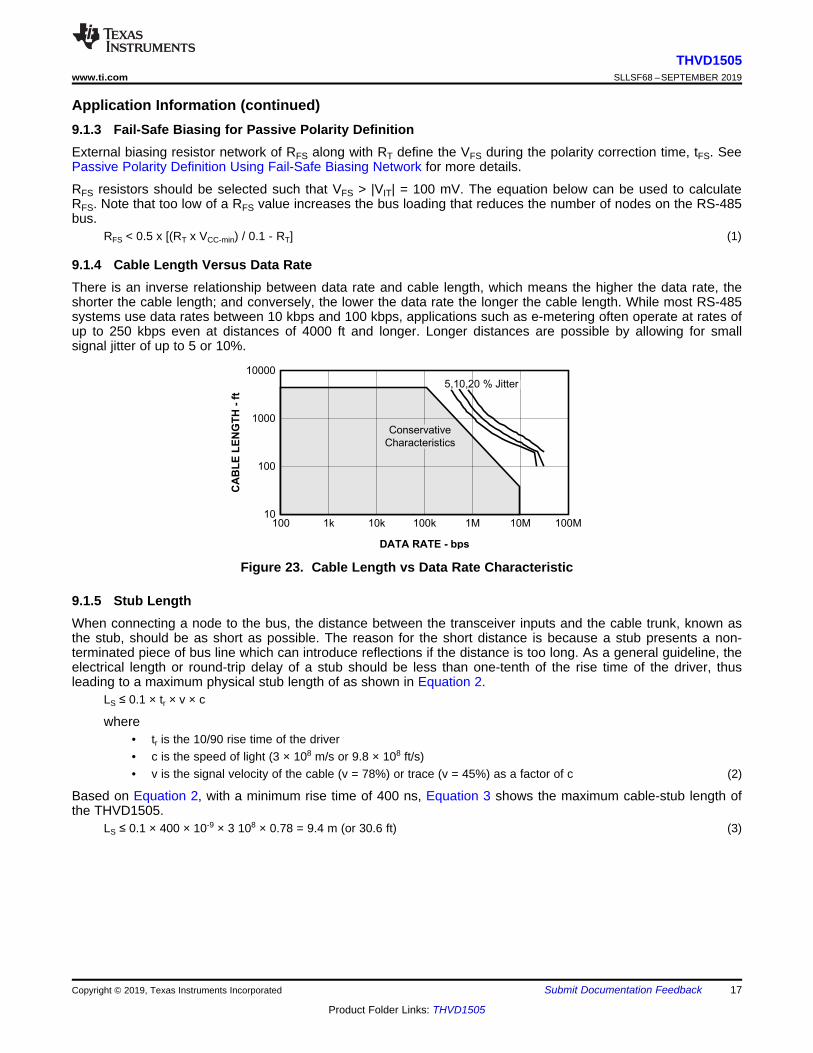
10000
1000
100
10
CA
BL
EL
EN
GT
H-
ft
100 1k 10k 100k 1M 10M 100M
DATA RATE - bps
Conservative
Characteristics
5,10,20 % Jitter
17
THVD1505www.ti.com SLLSF68 –SEPTEMBER 2019
Product Folder Links: THVD1505
Submit Documentation FeedbackCopyright © 2019, Texas Instruments Incorporated
Application Information (continued)9.1.3 Fail-Safe Biasing for Passive Polarity DefinitionExternal biasing resistor network of RFS along with RT define the VFS during the polarity correction time, tFS. SeePassive Polarity Definition Using Fail-Safe Biasing Network for more details.
RFS resistors should be selected such that VFS > |VIT| = 100 mV. The equation below can be used to calculateRFS. Note that too low of a RFS value increases the bus loading that reduces the number of nodes on the RS-485bus.
RFS < 0.5 x [(RT x VCC-min) / 0.1 - RT] (1)
9.1.4 Cable Length Versus Data RateThere is an inverse relationship between data rate and cable length, which means the higher the data rate, theshorter the cable length; and conversely, the lower the data rate the longer the cable length. While most RS-485systems use data rates between 10 kbps and 100 kbps, applications such as e-metering often operate at rates ofup to 250 kbps even at distances of 4000 ft and longer. Longer distances are possible by allowing for smallsignal jitter of up to 5 or 10%.
Figure 23. Cable Length vs Data Rate Characteristic
9.1.5 Stub LengthWhen connecting a node to the bus, the distance between the transceiver inputs and the cable trunk, known asthe stub, should be as short as possible. The reason for the short distance is because a stub presents a non-terminated piece of bus line which can introduce reflections if the distance is too long. As a general guideline, theelectrical length or round-trip delay of a stub should be less than one-tenth of the rise time of the driver, thusleading to a maximum physical stub length of as shown in Equation 2.
LS ≤ 0.1 × tr × v × c
where• tr is the 10/90 rise time of the driver• c is the speed of light (3 × 10⁸ m/s or 9.8 × 108 ft/s)• v is the signal velocity of the cable (v = 78%) or trace (v = 45%) as a factor of c (2)
Based on Equation 2, with a minimum rise time of 400 ns, Equation 3 shows the maximum cable-stub length ofthe THVD1505.
LS ≤ 0.1 × 400 × 10-9 × 3 108 × 0.78 = 9.4 m (or 30.6 ft) (3)

RC RD
CS
High-VoltagePulse
Generator
DeviceUnderTest
Curr
ent
-A
40
35
30
25
20
15
10
5
0
Time - ns
0 50 100 150 200 250 300
10kV IEC
10kV HBM
330
(1.5k)
150pF
(100pF)
50M
(1M)
Copyright © 2016, Texas Instruments Incorporated
R
A B
R RE DE D
D
LS
18
THVD1505SLLSF68 –SEPTEMBER 2019 www.ti.com
Product Folder Links: THVD1505
Submit Documentation Feedback Copyright © 2019, Texas Instruments Incorporated
Application Information (continued)
Figure 24. Stub Length
9.1.6 Transient ProtectionThe bus terminals of the THVD1505 transceiver family possess on-chip ESD protection against ±16 kV HBM, ±8kV IEC 61000-4-2 contact discharge and ±2 kV IEC 61000-4-4 EFT. The International ElectrotechnicalCommission (IEC) ESD test is far more severe than the HBM ESD test. The 50% higher charge capacitance, CS,and 78% lower discharge resistance, RD of the IEC model produce significantly higher discharge currents thanthe HBM model.
Figure 25. HBM and IEC ESD Models and Currents in Comparison (HBM Values in Parenthesis)
The on-chip implementation of IEC ESD and EFT protection significantly increases the robustness of equipment.Common discharge events occur because of human contact with connectors and cables. EFTs are generallycaused by relay-contact bounce or the interruption of inductive loads.
Surge transients often result from lightning strikes (direct strike or an indirect strike which induce voltages andcurrents), or the switching of power systems, including load changes and short circuit switching. These transientsare often encountered in industrial environments, such as factory automation and power-grid systems.
Figure 26 compares the pulse-power of the EFT and surge transients with the power caused by an IEC ESDtransient. The left hand diagram shows the relative pulse-power for a 0.5-kV surge transient and 4-kV EFTtransient, both of which dwarf the 10-kV ESD transient visible in the lower-left corner. 500-V surge transients arerepresentative of events that may occur in factory environments in industrial and process automation. The righthand diagram shows the pulse-power of a 6-kV surge transient, relative to the same 0.5-kV surge transient. 6-kVsurge transients are most likely to occur in power generation and power-grid systems.
Designers may choose to implement protection against longer duration surge transients. Figure 28 suggests twocircuit designs providing protection against short and long duration surge transients. Table 3 lists the bill ofmaterials for the external protection devices.

100
0.1
0.01
10
1
10-3
10-4
10-5
10-6
Pu
lse E
nerg
y -
Jo
ule
0.5 1 2 4 6 8 10
Peak Pulse Voltage - kV
1000
ESD
EFT
Surge
15
EFT Pulse Train
Pu
lse
Po
we
r -
kW
22
20
18
16
14
12
10
8
6
4
2
0
Time - sμ
0 5 10 15 20 25 30 35 40
0.5kV Surge
10kV ESD
4kV EFT
Pu
lse
Po
we
r -
MW
2.2
2.0
1.8
1.6
1.4
1.2
1.0
0.8
0.6
0.4
0.2
0
Time - sμ
0 5 10 15 20 25 30 35 40
0.5kV Surge
6kV Surge
3.0
2.8
2.6
2.4
19
THVD1505www.ti.com SLLSF68 –SEPTEMBER 2019
Product Folder Links: THVD1505
Submit Documentation FeedbackCopyright © 2019, Texas Instruments Incorporated
Application Information (continued)
NOTEThe unit of the pulse-power changes from kW to MW, thus making the power of the 500-Vsurge transient almost dropping off the scale.
Figure 26. Power Comparison of ESD, EFT, and Surge Transients
In the case of surge transients, high-energy content is signified by long pulse duration and slow decaying pulsepower.
The electrical energy of a transient that is dumped into the internal protection cells of the transceiver is convertedinto thermal energy. This thermal energy heats the protection cells and literally destroys them, thus destroyingthe transceiver. Figure 27 shows the large differences in transient energies for single ESD, EFT, and surgetransients as well as for an EFT pulse train, commonly applied during compliance testing.
Figure 27. Comparison of Transient Energies

R
RE
DE
D
B
A
Vcc
GND
1
2
3
4
7
6
5
Vcc
10k
10k
XCVR
TVS
R1
R2
TBU1
TBU2
MOV1
MOV2
8
Vcc
0.1�FRxD
TxD
DIR
MCU
R
RE
DE
D
B
A
Vcc
GND
1
2
3
4
7
6
5
Vcc
10k
10k
XCVR
TVS
R1
R2
8
Vcc
0.1�FRxD
TxD
DIR
MCU
Copyright © 2016, Texas Instruments Incorporated
20
THVD1505SLLSF68 –SEPTEMBER 2019 www.ti.com
Product Folder Links: THVD1505
Submit Documentation Feedback Copyright © 2019, Texas Instruments Incorporated
Application Information (continued)
(1) See Third Party Disclaimer
Table 3. List of ComponentsDEVICE FUNCTION ORDER NUMBER (1) MANUFACTURER
XCVR 5-V, 1-Mbps RS-485 Transceiver THVD1505DR TIR1, R2 10-Ω, Pulse-Proof Thick-Film Resistor CRCW0603010RJNEAHP Vishay
TVS Bidirectional 400-W Transient VoltageSuppressor CDSOT23-SM712 Bourns
TBU1, TBU2 Bidirectional 200mA Transient Blocking Unit TBU-CA-065-200-WH Bourns
MOV1, MOV2 200-mA Transient Blocking Unit 200-V, Metal-Oxide Varistor MOV-10D201K Bourns
Figure 28. Transient Protections Against Surge Transients
The left circuit shown in Figure 28 provides surge protection of 1-kV transients, while the right protection circuitscan withstand surge transients of 5 kV.

THVD1505
21
THVD1505www.ti.com SLLSF68 –SEPTEMBER 2019
Product Folder Links: THVD1505
Submit Documentation FeedbackCopyright © 2019, Texas Instruments Incorporated
9.2 Typical ApplicationMany RS-485 networks use isolated bus nodes to prevent the creation of unintended ground loops and theirdisruptive impact on signal integrity. An isolated bus node typically includes a micro controller that connects tothe bus transceiver through a multi-channel, digital isolator (Figure 29).
A. See Table 3.
Figure 29. Isolated Bus Node With Transient Protection
9.2.1 Design RequirementsExample Application: Isolated Bus Node with Transient Protection• RS-485-compliant bus interface.• Galvanic isolation of both signal and power supply lines.• Able to withstand surge transients up to 1 kV (per IEC 61000-4-5).• Full control of data flow on bus in order to prevent contention (for half-duplex communication).
9.2.2 Detailed Design ProcedurePower isolation is accomplished using the push-pull transformer driver SN6501, a low-cost LDO and TLV70733.
Signal isolation uses the quadruple digital isolator ISO7741. Notice that both enable inputs, EN1 and EN2, arepulled-up via 4.7-kΩ resistors to limit input currents during transient events.
While the transient protection is similar to the one in Figure 28 (left circuit), an additional high-voltage capacitordiverts transient energy from the floating RS-485 common further towards protective earth (PE) ground. Thisdiversion is necessary as noise transients on the bus are usually referred to Earth potential.
RVH refers to a high-voltage resistor, and in some applications even a varistor. This resistance is applied toprevent charging of the floating ground to dangerous potentials during normal operation.
Occasionally varistors are used instead of resistors in order to rapidly discharge CHV, if expected that fasttransients might charge CHV to high-potentials.

22
THVD1505SLLSF68 –SEPTEMBER 2019 www.ti.com
Product Folder Links: THVD1505
Submit Documentation Feedback Copyright © 2019, Texas Instruments Incorporated
Typical Application (continued)Note that the PE island represents a copper island on the PCB for the provision of a short, thick Earth wireconnecting this island to PE ground at the entrance of the power supply unit (PSU).
In equipment designs using a chassis, the PE connection is usually provided through the chassis itself. Typicallythe PE conductor is tied to the chassis at one end while the high-voltage components, CHV and RHV, areconnecting to the chassis at the other end.
9.2.3 Application Curve
Figure 30. Waveforms at 1 Mbps Operation, PRBS7 Data Pattern
Figure 31. Waveforms at 1 Mbps Operation, Clock Data Pattern

23
THVD1505www.ti.com SLLSF68 –SEPTEMBER 2019
Product Folder Links: THVD1505
Submit Documentation FeedbackCopyright © 2019, Texas Instruments Incorporated
10 Power Supply RecommendationsTo ensure reliable operation at all data rates and supply voltages, each supply should be decoupled with a 100-nF ceramic capacitor located as close to the supply pins as possible. This helps to reduce supply voltage ripplepresent on the outputs of switched-mode power supplies and also helps to compensate for the resistance andinductance of the PCB power planes.

MCU
R
R
Via to ground
THVD1505
JM
PR
R
R
C
5
6
6
1
4R
5
Via to VCC
TVS
75
24
THVD1505SLLSF68 –SEPTEMBER 2019 www.ti.com
Product Folder Links: THVD1505
Submit Documentation Feedback Copyright © 2019, Texas Instruments Incorporated
11 Layout
11.1 Layout Guidelines
11.1.1 Design and Layout Considerations For Transient ProtectionRobust and reliable bus node design often requires the use of external transient protection devices in order toprotect against surge transients that may occur in industrial environments. Since these transients have a widefrequency bandwidth (from approximately 3 MHz to 300 MHz), high-frequency layout techniques should beapplied during PCB design.1. Place the protection circuitry close to the bus connector to prevent noise transients from propagating across
the board.2. Use Vcc and ground planes to provide low inductance. Note that high frequency currents follow the path of
least impedance and not the path of least resistance.3. Design the protection components into the direction of the signal path. Do not force the transients currents to
divert from the signal path to reach the protection device.4. Apply 100 to 220-nF decoupling capacitors as close as possible to the VCC pins of transceiver and UART or
controller ICs on the board.5. Use at least two vias for VCC and ground connections of decoupling capacitors and protection devices to
minimize effective via inductance.6. Use 1 to 10-k pull-up or pull-down resistors for enable lines to limit noise currents in theses lines during
transient events.7. Insert pulse-proof resistors into the A and B bus lines if the TVS clamping voltage is higher than the specified
maximum voltage of the transceiver bus terminals. These resistors limit the residual clamping current into thetransceiver and prevent it from latching up.– While pure TVS protection is sufficient for surge transients up to 1 kV, higher transients require metal-
oxide varistors (MOVs) which reduce the transients to a few-hundred volts of clamping voltage, andtransient blocking units (TBUs) that limit transient current to about 200 mA.
11.2 Layout Example
Figure 32. THVD1505 Layout Example

25
THVD1505www.ti.com SLLSF68 –SEPTEMBER 2019
Product Folder Links: THVD1505
Submit Documentation FeedbackCopyright © 2019, Texas Instruments Incorporated
12 Device and Documentation Support
12.1 Device Support
12.1.1 Third-Party Products DisclaimerTI'S PUBLICATION OF INFORMATION REGARDING THIRD-PARTY PRODUCTS OR SERVICES DOES NOTCONSTITUTE AN ENDORSEMENT REGARDING THE SUITABILITY OF SUCH PRODUCTS OR SERVICESOR A WARRANTY, REPRESENTATION OR ENDORSEMENT OF SUCH PRODUCTS OR SERVICES, EITHERALONE OR IN COMBINATION WITH ANY TI PRODUCT OR SERVICE.
12.2 Receiving Notification of Documentation UpdatesTo receive notification of documentation updates, navigate to the device product folder on ti.com. In the upperright corner, click on Alert me to register and receive a weekly digest of any product information that haschanged. For change details, review the revision history included in any revised document.
12.3 Community ResourcesTI E2E™ support forums are an engineer's go-to source for fast, verified answers and design help — straightfrom the experts. Search existing answers or ask your own question to get the quick design help you need.
Linked content is provided "AS IS" by the respective contributors. They do not constitute TI specifications and donot necessarily reflect TI's views; see TI's Terms of Use.
12.4 TrademarksE2E is a trademark of Texas Instruments.
12.5 Electrostatic Discharge CautionThese devices have limited built-in ESD protection. The leads should be shorted together or the device placed in conductive foamduring storage or handling to prevent electrostatic damage to the MOS gates.
12.6 GlossarySLYZ022 — TI Glossary.
This glossary lists and explains terms, acronyms, and definitions.
13 Mechanical, Packaging, and Orderable InformationThe following pages include mechanical, packaging, and orderable information. This information is the mostcurrent data available for the designated devices. This data is subject to change without notice and revision ofthis document. For browser-based versions of this data sheet, refer to the left-hand navigation.

PACKAGE OPTION ADDENDUM
www.ti.com 10-Dec-2020
Addendum-Page 1
PACKAGING INFORMATION
Orderable Device Status(1)
Package Type PackageDrawing
Pins PackageQty
Eco Plan(2)
Lead finish/Ball material
(6)
MSL Peak Temp(3)
Op Temp (°C) Device Marking(4/5)
Samples
THVD1505DR ACTIVE SOIC D 8 2500 RoHS & Green NIPDAU Level-1-260C-UNLIM -40 to 125 1505
(1) The marketing status values are defined as follows:ACTIVE: Product device recommended for new designs.LIFEBUY: TI has announced that the device will be discontinued, and a lifetime-buy period is in effect.NRND: Not recommended for new designs. Device is in production to support existing customers, but TI does not recommend using this part in a new design.PREVIEW: Device has been announced but is not in production. Samples may or may not be available.OBSOLETE: TI has discontinued the production of the device.
(2) RoHS: TI defines "RoHS" to mean semiconductor products that are compliant with the current EU RoHS requirements for all 10 RoHS substances, including the requirement that RoHS substancedo not exceed 0.1% by weight in homogeneous materials. Where designed to be soldered at high temperatures, "RoHS" products are suitable for use in specified lead-free processes. TI mayreference these types of products as "Pb-Free".RoHS Exempt: TI defines "RoHS Exempt" to mean products that contain lead but are compliant with EU RoHS pursuant to a specific EU RoHS exemption.Green: TI defines "Green" to mean the content of Chlorine (Cl) and Bromine (Br) based flame retardants meet JS709B low halogen requirements of <=1000ppm threshold. Antimony trioxide basedflame retardants must also meet the <=1000ppm threshold requirement.
(3) MSL, Peak Temp. - The Moisture Sensitivity Level rating according to the JEDEC industry standard classifications, and peak solder temperature.
(4) There may be additional marking, which relates to the logo, the lot trace code information, or the environmental category on the device.
(5) Multiple Device Markings will be inside parentheses. Only one Device Marking contained in parentheses and separated by a "~" will appear on a device. If a line is indented then it is a continuationof the previous line and the two combined represent the entire Device Marking for that device.
(6) Lead finish/Ball material - Orderable Devices may have multiple material finish options. Finish options are separated by a vertical ruled line. Lead finish/Ball material values may wrap to twolines if the finish value exceeds the maximum column width.
Important Information and Disclaimer:The information provided on this page represents TI's knowledge and belief as of the date that it is provided. TI bases its knowledge and belief on informationprovided by third parties, and makes no representation or warranty as to the accuracy of such information. Efforts are underway to better integrate information from third parties. TI has taken andcontinues to take reasonable steps to provide representative and accurate information but may not have conducted destructive testing or chemical analysis on incoming materials and chemicals.TI and TI suppliers consider certain information to be proprietary, and thus CAS numbers and other limited information may not be available for release.
In no event shall TI's liability arising out of such information exceed the total purchase price of the TI part(s) at issue in this document sold by TI to Customer on an annual basis.
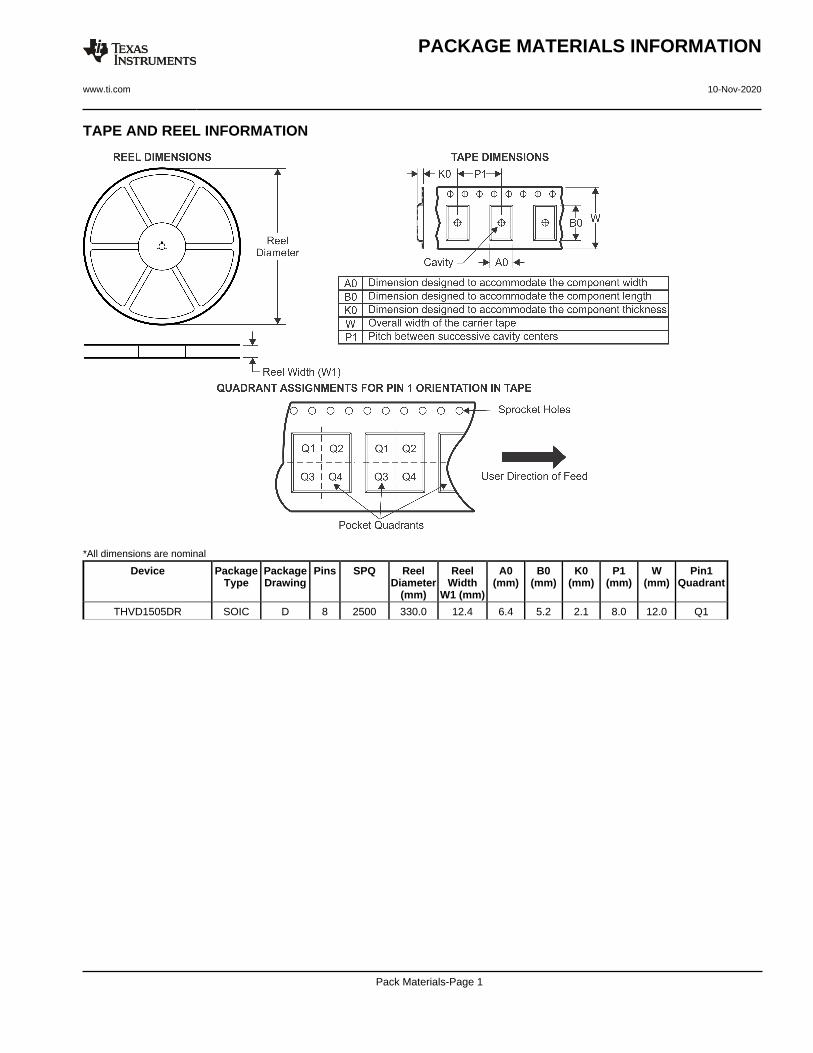
TAPE AND REEL INFORMATION
*All dimensions are nominal
Device PackageType
PackageDrawing
Pins SPQ ReelDiameter
(mm)
ReelWidth
W1 (mm)
A0(mm)
B0(mm)
K0(mm)
P1(mm)
W(mm)
Pin1Quadrant
THVD1505DR SOIC D 8 2500 330.0 12.4 6.4 5.2 2.1 8.0 12.0 Q1
PACKAGE MATERIALS INFORMATION
www.ti.com 10-Nov-2020
Pack Materials-Page 1

*All dimensions are nominal
Device Package Type Package Drawing Pins SPQ Length (mm) Width (mm) Height (mm)
THVD1505DR SOIC D 8 2500 853.0 449.0 35.0
PACKAGE MATERIALS INFORMATION
www.ti.com 10-Nov-2020
Pack Materials-Page 2
www.ti.com
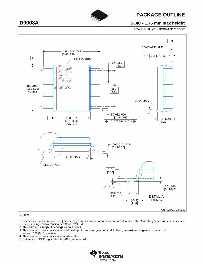
PACKAGE OUTLINE
C
.228-.244 TYP[5.80-6.19]
.069 MAX[1.75]
6X .050[1.27]
8X .012-.020 [0.31-0.51]
2X.150[3.81]
.005-.010 TYP[0.13-0.25]
0 - 8 .004-.010[0.11-0.25]
.010[0.25]
.016-.050[0.41-1.27]
4X (0 -15 )
A
.189-.197[4.81-5.00]
NOTE 3
B .150-.157[3.81-3.98]
NOTE 4
4X (0 -15 )
(.041)[1.04]
SOIC - 1.75 mm max heightD0008ASMALL OUTLINE INTEGRATED CIRCUIT
4214825/C 02/2019
NOTES: 1. Linear dimensions are in inches [millimeters]. Dimensions in parenthesis are for reference only. Controlling dimensions are in inches. Dimensioning and tolerancing per ASME Y14.5M. 2. This drawing is subject to change without notice. 3. This dimension does not include mold flash, protrusions, or gate burrs. Mold flash, protrusions, or gate burrs shall not exceed .006 [0.15] per side. 4. This dimension does not include interlead flash.5. Reference JEDEC registration MS-012, variation AA.
18
.010 [0.25] C A B
54
PIN 1 ID AREA
SEATING PLANE
.004 [0.1] C
SEE DETAIL A
DETAIL ATYPICAL
SCALE 2.800

www.ti.com
EXAMPLE BOARD LAYOUT
.0028 MAX[0.07]ALL AROUND
.0028 MIN[0.07]ALL AROUND
(.213)[5.4]
6X (.050 )[1.27]
8X (.061 )[1.55]
8X (.024)[0.6]
(R.002 ) TYP[0.05]
SOIC - 1.75 mm max heightD0008ASMALL OUTLINE INTEGRATED CIRCUIT
4214825/C 02/2019
NOTES: (continued) 6. Publication IPC-7351 may have alternate designs. 7. Solder mask tolerances between and around signal pads can vary based on board fabrication site.
METALSOLDER MASKOPENING
NON SOLDER MASKDEFINED
SOLDER MASK DETAILS
EXPOSEDMETAL
OPENINGSOLDER MASK METAL UNDER
SOLDER MASK
SOLDER MASKDEFINED
EXPOSEDMETAL
LAND PATTERN EXAMPLEEXPOSED METAL SHOWN
SCALE:8X
SYMM
1
45
8
SEEDETAILS
SYMM
www.ti.com
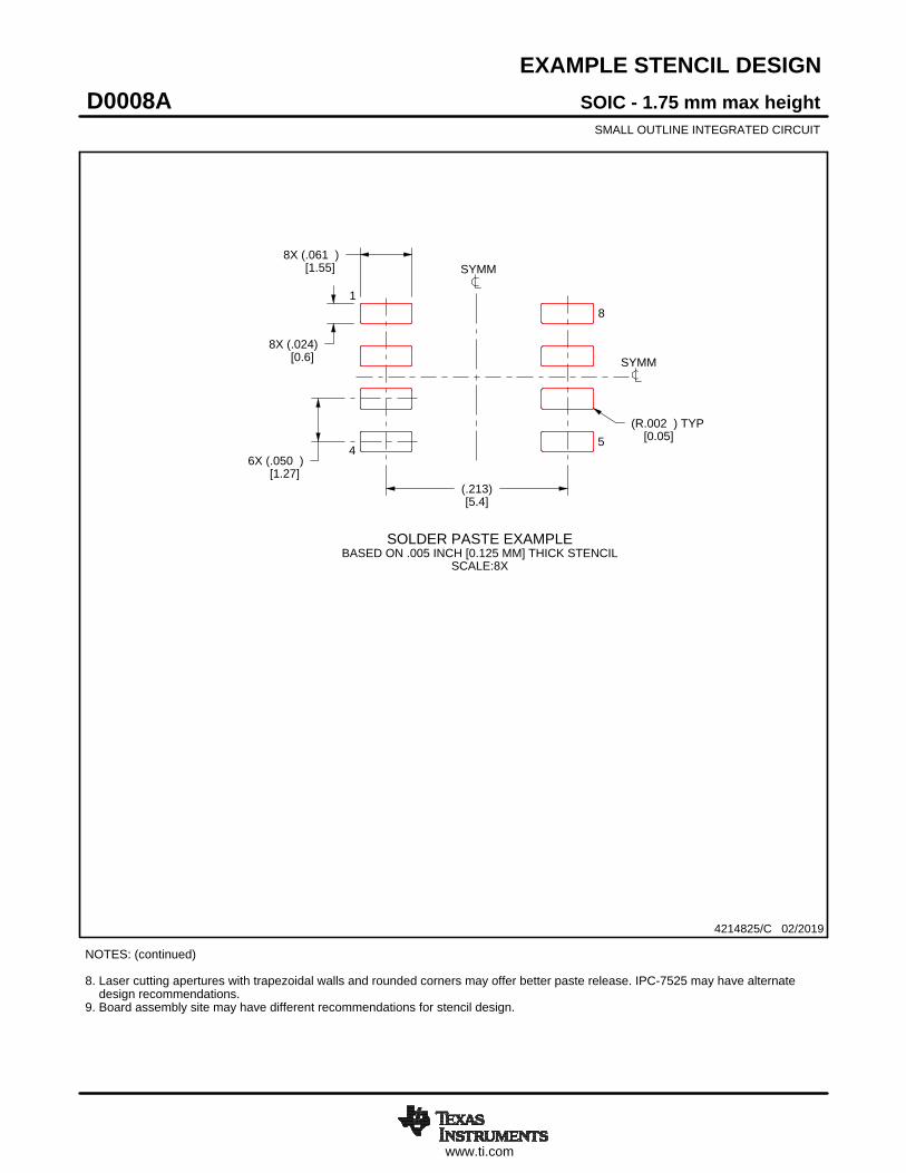
EXAMPLE STENCIL DESIGN
8X (.061 )[1.55]
8X (.024)[0.6]
6X (.050 )[1.27]
(.213)[5.4]
(R.002 ) TYP[0.05]
SOIC - 1.75 mm max heightD0008ASMALL OUTLINE INTEGRATED CIRCUIT
4214825/C 02/2019
NOTES: (continued) 8. Laser cutting apertures with trapezoidal walls and rounded corners may offer better paste release. IPC-7525 may have alternate design recommendations. 9. Board assembly site may have different recommendations for stencil design.
SOLDER PASTE EXAMPLEBASED ON .005 INCH [0.125 MM] THICK STENCIL
SCALE:8X
SYMM
SYMM
1
45
8

IMPORTANT NOTICE AND DISCLAIMER
TI PROVIDES TECHNICAL AND RELIABILITY DATA (INCLUDING DATASHEETS), DESIGN RESOURCES (INCLUDING REFERENCE DESIGNS), APPLICATION OR OTHER DESIGN ADVICE, WEB TOOLS, SAFETY INFORMATION, AND OTHER RESOURCES “AS IS” AND WITH ALL FAULTS, AND DISCLAIMS ALL WARRANTIES, EXPRESS AND IMPLIED, INCLUDING WITHOUT LIMITATION ANY IMPLIED WARRANTIES OF MERCHANTABILITY, FITNESS FOR A PARTICULAR PURPOSE OR NON-INFRINGEMENT OF THIRD PARTY INTELLECTUAL PROPERTY RIGHTS.These resources are intended for skilled developers designing with TI products. You are solely responsible for (1) selecting the appropriate TI products for your application, (2) designing, validating and testing your application, and (3) ensuring your application meets applicable standards, and any other safety, security, or other requirements. These resources are subject to change without notice. TI grants you permission to use these resources only for development of an application that uses the TI products described in the resource. Other reproduction and display of these resources is prohibited. No license is granted to any other TI intellectual property right or to any third party intellectual property right. TI disclaims responsibility for, and you will fully indemnify TI and its representatives against, any claims, damages, costs, losses, and liabilities arising out of your use of these resources.TI’s products are provided subject to TI’s Terms of Sale (www.ti.com/legal/termsofsale.html) or other applicable terms available either on ti.com or provided in conjunction with such TI products. TI’s provision of these resources does not expand or otherwise alter TI’s applicable warranties or warranty disclaimers for TI products.
Mailing Address: Texas Instruments, Post Office Box 655303, Dallas, Texas 75265Copyright © 2020, Texas Instruments Incorporated