THREE-DIMENSIONAL NANOBIOCOMPUTING · PDF fileAFRL-IF-RS-TR-2007-158 Final Technical Report...
51
AFRL-IF-RS-TR-2007-158 Final Technical Report June 2007 THREE-DIMENSIONAL NANOBIOCOMPUTING ARCHITECTURES WITH NEURONAL HYPERCELLS Microsystems & Nanotechnologies APPROVED FOR PUBLIC RELEASE; DISTRIBUTION UNLIMITED. STINFO COPY AIR FORCE RESEARCH LABORATORY INFORMATION DIRECTORATE ROME RESEARCH SITE ROME, NEW YORK
Transcript of THREE-DIMENSIONAL NANOBIOCOMPUTING · PDF fileAFRL-IF-RS-TR-2007-158 Final Technical Report...
AFRL-IF-RS-TR-2007-158 Final Technical Report June 2007 THREE-DIMENSIONAL NANOBIOCOMPUTING ARCHITECTURES WITH NEURONAL HYPERCELLS Microsystems & Nanotechnologies
APPROVED FOR PUBLIC RELEASE; DISTRIBUTION UNLIMITED.
STINFO COPY
AIR FORCE RESEARCH LABORATORY INFORMATION DIRECTORATE
ROME RESEARCH SITE ROME, NEW YORK
NOTICE AND SIGNATURE PAGE Using Government drawings, specifications, or other data included in this document for any purpose other than Government procurement does not in any way obligate the U.S. Government. The fact that the Government formulated or supplied the drawings, specifications, or other data does not license the holder or any other person or corporation; or convey any rights or permission to manufacture, use, or sell any patented invention that may relate to them. This report was cleared for public release by the Air Force Research Laboratory Rome Research Site Public Affairs Office and is available to the general public, including foreign nationals. Copies may be obtained from the Defense Technical Information Center (DTIC) (http://www.dtic.mil). AFRL-IF-RS-TR-2007-158 HAS BEEN REVIEWED AND IS APPROVED FOR PUBLICATION IN ACCORDANCE WITH ASSIGNED DISTRIBUTION STATEMENT. FOR THE DIRECTOR: /s/ /s/ THOMAS E. RENZ JAMES A. COLLINS, Deputy Chief Work Unit Manager Advanced Computing Division Information Directorate This report is published in the interest of scientific and technical information exchange, and its publication does not constitute the Government’s approval or disapproval of its ideas or findings.

REPORT DOCUMENTATION PAGE Form Approved OMB No. 0704-0188
Public reporting burden for this collection of information is estimated to average 1 hour per response, including the time for reviewing instructions, searching data sources, gathering and maintaining the data needed, and completing and reviewing the collection of information. Send comments regarding this burden estimate or any other aspect of this collection of information, including suggestions for reducing this burden to Washington Headquarters Service, Directorate for Information Operations and Reports, 1215 Jefferson Davis Highway, Suite 1204, Arlington, VA 22202-4302, and to the Office of Management and Budget, Paperwork Reduction Project (0704-0188) Washington, DC 20503. PLEASE DO NOT RETURN YOUR FORM TO THE ABOVE ADDRESS. 1. REPORT DATE (DD-MM-YYYY)
JUN 2007 2. REPORT TYPE
Final 3. DATES COVERED (From - To)
Apr 06 – Jan 07 5a. CONTRACT NUMBER
FA8750-06-C-0058
5b. GRANT NUMBER
4. TITLE AND SUBTITLE THREE-DIMENSIONAL NANOBIOCOMPUTING ARCHITECTURES WITH NEURONAL HYPERCELLS
5c. PROGRAM ELEMENT NUMBER 61101E
5d. PROJECT NUMBER NBGQ
5e. TASK NUMBER 10
6. AUTHOR(S) Sergey Lyshevski, Vlad Shmerko, Svetlana Yanushkevich and Marina Lyshevski
5f. WORK UNIT NUMBER 13
7. PERFORMING ORGANIZATION NAME(S) AND ADDRESS(ES) Microsystems & Nanotechnologies 70 Angel Path Webster NY 14580
8. PERFORMING ORGANIZATION REPORT NUMBER
10. SPONSOR/MONITOR'S ACRONYM(S)
9. SPONSORING/MONITORING AGENCY NAME(S) AND ADDRESS(ES) AFRL/IFTC 525 Brooks Rd Rome NY 13441-4505
11. SPONSORING/MONITORING AGENCY REPORT NUMBER AFRL-IF-RS-TR-2007-158
12. DISTRIBUTION AVAILABILITY STATEMENT APPROVED FOR PUBLIC RELEASE; DISTRIBUTION UNLIMITED. PA# 07-332
13. SUPPLEMENTARY NOTES 14. ABSTRACT Microsystems and Nanotechnologies investigated a novel 3D3 (Hardware–Software–Nanotechnology) technology to design super-high-performance computing and processing platforms utilizing molecular hardware within an enabling organization and architecture. The design technology is based on utilizing a three-fold solution: (1) Innovative hardware - 3D-topology molecular hardware (device-module-system) within enabling organization/architecture solutions utilizing molecular integrated circuits (MICs); (2) Novel software - computer-aided-design (CAD) tools supported by new synthesis and design methods; (3) Nanotechnology - molecular fabrication technology. The technology departs from conventional planar ICs design (VLSI, ULSI and post ULSI), von Neumann architectures, and CMOS fabrication. Novel solutions of massive parallel distributed computing and processing (pipelined due to systolic processing) were utilized using devised 3D hypercubes (data structure assemblies) and neuronal hypercells (ℵhypercells) to implement designed MICs as molecular electronics hardware. Novel highly-efficient synthesis taxonomy and design concepts were developed and demonstrated. The design was accomplished utilizing linear decision diagrams and linear systolic arrays. Fundamental and applied research were integrated within innovative computing and molecular electronics technologies developing representative CAD tools and proof-of-concept software. 15. SUBJECT TERMS Molecular Computing, Molecular Electronics, Nanoelectronics, Molecular Devices, Molecular Electronics Design
16. SECURITY CLASSIFICATION OF: 19a. NAME OF RESPONSIBLE PERSON Tom Renz
a. REPORT U
b. ABSTRACT U
c. THIS PAGE U
17. LIMITATION OF ABSTRACT
UL
18. NUMBER OF PAGES
51 19b. TELEPHONE NUMBER (Include area code)
Standard Form 298 (Rev. 8-98)
Prescribed by ANSI Std. Z39.18

i
REPORT DOCUMENTATION PAGE This contract started April 11, 2006. The overall objective was to start the development of a novel 3D3 (Hardware–Software–Nanotechnology) technology for super-high-performance three-dimensional (3D) molecular/biomolecular computing and processing platforms to accomplish demanding mission-specific computing to support Air Force tasks. The specific objectives were: 1. Utilizing a unified bottom-up/top-down synthesis taxonomy, design super-high-performance
computing (processing) platforms implemented using molecular integrated circuits (MICs). Devise innovative organizations/architectures and assess 3D3 technology researching novel hardware, software, design methods and molecular electronics (nanotechnology) solutions.
2. Develop and demonstrate logic design methods in synthesis of 3D MICs for computing platforms. Perform the 3D-centered design of super-complex combinational circuits by using hypercubes as homogeneous aggregated data structure assemblies. Assess the technology-centric Super Large Scale Integration (SLSI), and analyze the implementation of MICs utilizing neuronal hypercells (ℵhypercells) as the molecular hardware primitives. Develop and apply performance indexes to evaluate molecular electronics and MICs.
3. Propose molecular electronic devices (MEdevices). For a multi-terminal MEdevice, perform modeling and analysis of electron transport to assess the applicability of MEdevices for molecular gates (Mgates), ℵhypercells and MICs. Develop and demonstrate the fundamentals of CAD-supported synthesis, design, analysis and evaluation methods. Start the development of proof-of-concept CAD tools. The representative CAD software should perform illustrative design and analysis tasks at the device and system levels. Demonstrate the design for combinational circuits, including a 8- or 9-bit arithmetic logic unit (ALU).
For the SOW Task 1, Microsystems and Nanotechnologies developed and demonstrated a nanotechnology-centric synthesis taxonomy to design super-high-performance computing and processing platforms. We developed a unified bottom-up and top-down synthesis taxonomy to concurrently support 3D3 technology. This synthesis taxonomy was evaluated emphasizing different molecular (nanotechnology) hardware and processing paradigms. For the SOW Task 2, Microsystems and Nanotechnologies developed and demonstrated a new computationally efficient method in the design of MICs. This technology-centric design results in the synthesis of complex MICs using hypercubes to represent data structures in 3D, and implementation of MICs by ℵhypercells. The proposed concept allows one to design and implement innovative organizations and architectures. The design is supported by developing proof-of-concept software supporting the 3D3 technology. The performance estimates were derived and estimated in order to obtain coherent indexes and metrics at the device and system levels. For the SOW Task 3, Microsystems and Nanotechnologies examined the feasibility, soundness and baseline performance characteristics of prospective molecular and biomolecular devices which form molecular and biomolecular processing hardware. With emphasis on the foreseen synthesis technologies, fabrication feasibility, soundness and affordability, we proposed to utilize monocyclic organic molecules as multi-terminal solid MEdevices to engineer Mgates which form ℵhypercells and MICs. Electron transport in a solid MEdevice was examined to obtain baseline device characteristics and performance estimates. The representative proof-of-concept CAD tools in the logic design of MICs were developed and demonstrated for ALUs and other combinational circuits.
ii
TABLE OF CONTENTS List of Figures and Tables ............................................................................................... iii Summary ………..………………………………………………………………….…... v 1.0 Introduction …………………………………………………………………………….. 1 2.0 Methods, Assumptions, and Procedures ………………………………………….….… 2 3.0 Results and Discussions ………………………………………………………………… 3
3.1 Molecular Computing and Processing Platforms: Introduction and Performance Estimates al ICs …………….……………………………………………………. 4 3.1.1 Microelectronics and Molecular Electronics …………………………. 4
3.1.2 Performance Estimates ……………………………………………….. 5
3.2 Synthesis Taxonomy ……………………………………………….……………. 8 3.3 Logic Design of Molecular ICs …………………………………………………. 13
3.3.1 Design of 3D Molecular Integrated Circuits: Data Structure, Decision Diagram and Hypercubes ………. …………………………. 13 3.3.2 Hypercube Design …………..………………………………………… 15 3.3.3 Electronic Molecular Devices, Gates and ℵHypercells: MIC Prospective 17 3.4 Multi-Terminal Molecular Electronic Devices ……………………………..…… 19 3.4.1 Biomolecules as Molecular Electronic Devices …………………...…. 19 3.4.2 Multi-Terminal Quantum Effect Molecular Electronic Devices ……… 24 3.5 Proof-of-Concept CAD and Software Developments …….……………….……. 30
3.5.1 CAD and Software Developments for SLSI Design …………………. 30 3.5.2 Three-Dimensional Design of ICs and Proof-of-Concept ALU ……… 33
4.0 Conclusions …………..……………………………………………………………..….. 37 References ……………………………………………..……………………………..… 38 PIs Recent Publications as Directly Related to the Problem Solved and Technology Developed ……………………………………………………………… 40 List of Abbreviations, and Acronyms ……………………………………….................... 42

iii
LIST OF FIGURES AND TABLES
Figure 1. Envisioned molecular (nano) electronics advancements and Moore’s laws for microelectronics ......................................................................................................... 4 Figure 2. Towards molecular electronics and computing (processing) platforms: ………………. 8
• Revolutionary advancements: From 2D microelectronics to 3D molecular electronics • Evolutionary developments: From biomolecular to solid MEdevices
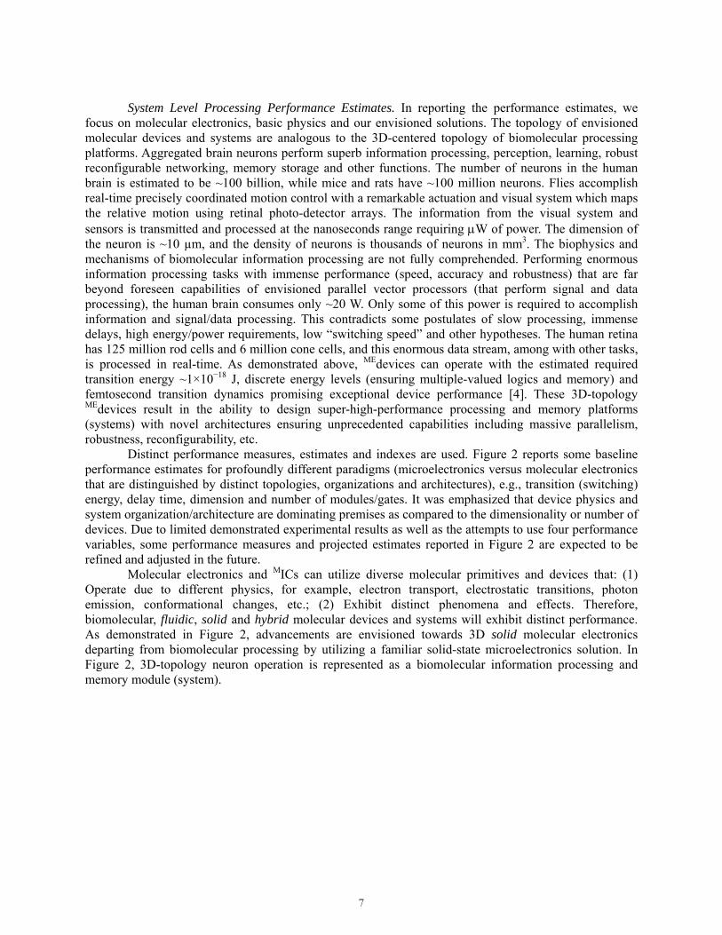
Figure 3. (a) Three-dimensional molecular electronics: Hypercubes Dijk implemented by ……… 9 ℵhypercells (atomic or molecular aggregates) composed from Mgates that integrate multi-terminal MEdevices engineered from atomic complexes; (b) Concurrent synthesis and design at system, subsystem and gate (device) levels.
Figure 4. Top-down and bottom-up synthesis taxonomy with x-design flow-map .......................... 10
Figure 5. Processing and memory platforms: Fused processing-and-memory organization and reconfigurable networking-and-processing neuromorphological architecture …….. 11 Figure 6. Molecular gate schematic …………………..................................................................... 11 Figure 7. Reconfigurable routing and networking …………......................................................... 12 Figure 8. Three-dimensional ℵhypercells and ℵhypercells aggregate forming MICs ............................ 15 Figure 9. Hypercube which implements function f .......................................................................... 17 Figure 10. Circuit schematics of two-input MNOR and MNAND gates .......................................... 18 Figure 11. (a) ℵHypercell schematics with two- and multi-terminal MEdevices; ………………….. 18 (b) Implementation of the ℵhypercell utilizing polypeptides with interconnected side R groups; (c) Implementation of the ℵhypercell by Mijk with eight side groups Sijk. Figure 12. MGate (MNAND) mapped by a single ℵhypercell and its implementation …………….. 19 Figure 13. a) Double-stranded DNA with two electrodes ………………………………………… 20 b) G4-DNA complex as a possible MEdevice Figure 14. Symmetric and asymmetric I–V characteristics ………………………………………. 21 Figure 15. Protein tertiary structure with weak and strong bonds ……………………………….. 22 Figure 16. (a) PolyG FET with a channel formed by the adsorbed polyG (dG(C10)2)n; …………. 23 (b) CMOS MOSFET
Figure 17. One-dimensional potential energy profile and quasi-Fermi levels in the double-barrier single-well heterojunction transistors …………………………………………………………….. 24
iv
Figure 18. I–V characteristic for a Au–C16H33Q-3CNQ monolayer–Au …………………………. 25 Figure 19. Molecules as potential two-terminal MEdevices ………………………………………. 25 (atoms are colored as: H – green, C – cyan, S – yellow and Au – magenta). (a) 1,4-phenyledithiol molecule and functionalized 1,4-phenyledithiol molecule; (b) 1,4-phenylenedimethanethiol molecule Figure 20. 1,3,5-triazine-2,4,6-trithiol molecules, H3TMT molecule, and functionalized H3TMT molecule with three Au-S bonds to form three terminals ensuring interconnect ………………… 25 Figure 21. Monocyclic molecule as a multi-terminal MEdevice ....................................................... 26 Figure 22. MAND and MNAND gates comprised from cyclic molecules …………………………. 27 Figure 23. Molecular gates: Minverter, MAND, MNAND, MOR, MNOR, MXOR and MMUX which can be utilized in the implementation of ℵhypercells …………………………………………….. 27 Figure 24. Three-terminal MEdevice comprised from a cyclic molecule with a carbon interconnecting framework ............................................................................................................... 28 Figure 25. Charge distribution ρ(r) ……………………………………………………………….. 28 Figure 26. Multiple-valued I–V characteristics …………………………………………………… 29 Figure 27. Six-terminal MEdevices ………………………………………………………………… 29 Figure 28. (a) Command Window of the LWDD Package to perform design of ICs in 3D;
(b) Design of c17 circuit, and c17 implementation using MNAND gates ……………. 31 Figure 29. Design of an 8-bit ALU (c880) ………………………………………………………… 32 Figure 30. Design of 3D MICs using interactive WindowIT software that performs integration, aggregation and visualization …………………………………………………………………….. 34
Figure 31. High-level model for a 9-bit ALU (c5315 circuit) ……………………………………. 35
Figure 32. Design of a 9-bit ALU ………………………………………………………………… 36 Table 1. Design summary (number of nodes, levels and CPU time) for BDD, WDD and LWDD .. 34 Table 2. Numerical results for 3D ICs …......................................................................................... 34

v
SUMMARY
Under USAF contract, Microsystems and Nanotechnologies performed research and technology development in three-dimensional (3D) computing architectures. The major accomplishments were: 1. A unified bottom-up/top-down synthesis taxonomy was developed accomplishing a coherent
design of an innovative computing platform implemented using Molecular Integrated Circuits (MICs) within an enabling organization and architecture. Reconfigurable networking-and-processing was provided by a neuromorphological architecture, fused processing-and-memory organization, and molecular hardware. This project integrated novel hardware, software, design methods, molecular electronics and nanotechnology (envisioned molecular synthesis and fabrication) within the proposed enabling 3D3 (Hardware–Software–Nanotechnology) technology.
2. A novel concept in the design of Integrated Circuits (ICs) and MICs in 3D space was developed and demonstrated. The proposed Super Large Scale Integration (SLSI) design was supported by the software developed. The design was performed for ICs by utilizing hypercubes (enhancing the design and data structure capabilities) within the envisioned molecular implementation by neuronal hypercells (ℵhypercells). Hypercubes (ICs design) and ℵhypercells (MICs implementation by molecular processing/memory hardware primitives) were designed. The performance and capabilities were assessed at device and system levels. Aggregated ℵhypercells form 3D ℵhypercell lattices implementing processing platforms. At the system level, benchmarking ICs, which have been widely used to evaluate and assess Very Large Scale Integration (VLSI) and Ultra Large Scale Integration (ULSI) designs, were examined as proof-of-concept 3D MICs.
3. Biomolecular and molecular processing hardware solutions were studied. Organic molecules form complexes which can be utilized as enabling molecular electronic devices (MEdevices). Molecular gates (Mgates) and ℵhypercells are formed using MEdevices. A 3D-topology solid MEdevice, engineered using monocyclic molecules, was modeled, simulated and analyzed. Components of the representative Computer Aided Design (CAD) software were developed to support the logic design tasks for 3D MICs. Combinational circuits, including 8- and 9-bit Arithmetic Logic Units (ALUs), were designed.
An enabling 3D3 technology was devised by utilizing a three-fold innovative solution: • Hardware - novel 3D-topology MEdevices, enabling system organizations and architectures; • Software - technology-centric CAD tools supported by new design methods to accomplish the
SLSI tasks for complex MICs; • Nanotechnology - molecular technology to synthesize ℵhypercells, MICs, modules and platforms. This 3D3 technology ensures super-high-performance processing. We focused on
development of a feasible, practical, affordable and superior technology for massive parallel distributed computing. The proposed technology allows one to perform design coherently integrating design and synthesis tasks at the device/gate and system levels.
We departed from the conventional, two-dimensional (2D) topology, organization and architecture of ICs and processing platforms, VLSI, ULSI and post ULSI design concepts and 2D Complimentary Metal Oxide Semiconductor, (CMOS) paradigms. A novel 3D3 technology, as implemented, will ensure: 1. Enormous military advantages because envisioned super-high-performance platforms will
guarantee information processing preeminence, computing superiority and memory supremacy; 2. Very strong commercial potential with immediate applications in design of new generations of
preeminent processors and memories; 3 Sound technology transfer feasibility to future Air Force systems.

1
1. INTRODUCTION The overall objective of this project was to start the development of a novel 3D3 (Hardware–Software–
Nanotechnology) technology for super-high-performance three-dimensional (3D) molecular/biomolecular computing and processing platforms to accomplish demanding mission-specific computing to support Air Force tasks. The specific objectives were: 1. Utilizing a unified bottom-up/top-down synthesis taxonomy, design super-high-performance
computing (processing) platforms implemented using molecular integrated circuits (MICs), devise innovative organizations/architectures and assess 3D3 technology researching novel hardware, software, design methods and molecular electronics (nanotechnology) solutions.
2. Develop and demonstrate logic design methods in synthesis of 3D MICs for computing platforms. Perform the 3D-centered design of super-complex combinational circuits by using hypercubes as homogeneous aggregated data structure assemblies. Assess technology-centric Super Large Scale Integration (SLSI), and analyze the implementation of MICs utilizing neuronal hypercells (ℵhypercells) as the molecular hardware primitives. Develop and apply performance indexes to evaluate molecular electronics and MICs.
3. Propose molecular electronic devices (MEdevices). For a multi-terminal MEdevice, perform modeling and analysis of electron transport to assess the applicability of MEdevices for molecular gates (Mgates), ℵhypercells and MICs. Develop and demonstrate the fundamentals of the CAD-supported synthesis, design, analysis and evaluation methods. Start the development of proof-of-concept CAD tools, where representative CAD software should perform illustrative design and analysis tasks at the device and system levels. Demonstrate the design for combinational circuits, including an 8- or 9-bit arithmetic logic unit (ALU).
Research at the system and device level was focused on the solution of a number of major problems. The technology developments were concentrated on the following three major tasks: 1. Develop a unified bottom-up and top-down synthesis taxonomy in order to design super-high-
performance computing (processing) platforms within novel 3D topologies and enabling organizations/architectures. Assess 3D3 technology which utilizes three major innovations, e.g., 3D MICs (molecular electronics), software, and molecular fabrication technology.
2. Propose and start development of a computationally efficient technology-centric SLSI design for circuits in 3D. Design MICs using hypercubes (data structures) and implement the designed MICs using ℵhypercells. Derive baseline performance estimates for the molecular electronic system.
3. Study biomolecular and molecular processing hardware solutions. Analyzing organic molecules, research multi-terminal MEdevices which comprise of Mgates and ℵhypercells. Model and obtain the baseline performance characteristics for a 3D-topology solid MEdevice. Start the developments of components of the representative CAD tools to support the logic design tasks for 3D MICs. Design combinational circuits, including an 8- or 9-bit ALU.
For the aforementioned major tasks, in order to complete the overall and specific objectives,
Microsystems and Nanotechnologies successfully accomplished the following:
For the Statement of Work, SOW Task 1, Microsystems and Nanotechnologies developed and demonstrated a nanotechnology-centric synthesis taxonomy to design super-high-performance computing and processing platforms. A unified bottom-up and top-down synthesis taxonomy to concurrently support
2
3D3 technology was developed. This synthesis taxonomy was evaluated emphasizing different molecular (nanotechnology) hardware and processing paradigms. For the SOW Task 2, Microsystems and Nanotechnologies developed and demonstrated a new computationally efficient method in the design of MICs. This technology-centric design results in the synthesis of complex MICs using hypercubes to represent data structures in 3D, and implementation of MICs by ℵhypercells. The proposed concept allows one to design and implement innovative organizations and architectures. The design was accomplished by developing proof-of-concept software supporting the 3D3 technology. Performance characteristics were derived or estimated in order to obtain coherent indexes and metrics at the device and system levels. For the SOW Task 3, Microsystems and Nanotechnologies examined the feasibility, soundness and baseline performance characteristics of prospective molecular and biomolecular devices which form molecular and biomolecular processing hardware. With the emphasis on foreseen synthesis technologies, fabrication feasibility, soundness and affordability, models of monocyclic organic molecules were utilized as multi-terminal solid MEdevices to engineer Mgates which form ℵhypercells and MICs. The electron transport in a solid MEdevice was modeled to obtain the baseline device characteristics and performance estimates. The representative proof-of-concept CAD tools in the logic design of MICs were developed and demonstrated for ALUs and other combinational circuits. 2. METHODS, ASSUMPTIONS, AND PROCEDURES
Solution (Methods) – An innovative 3D3 technology was based on the design of computing (processing) platforms and MICs utilizing a three-fold solution:
1. Novel hardware utilizing enabling 3D topologies, organizations and architectures; 2. New software and technology-centric CAD tools supported by advanced design methods
to perform SLSI design, 3. Nanotechnology-centered fabrication and implementation of molecular processing
hardware. This led to:
1. New organization and enabling architectures coherently supported by the SLSI design of MICs utilizing a technology-centric software and CAD tools;
2. Novel device physics and enabling device/system capabilities utilizing novel phenomena, effects and abilities of 3D-topology MEdevices and MICs;
3. Bottom-up fabrication. The 3D3 technology model developed in this project provides evidence of soundness, feasibility
and achievable super-high-performance reaching the fundamental limits of quantum mechanics (molecular device level) and systems capabilities (novel topologies/organizations/architectures). This project focused on development of a feasible, practical, affordable and superior technology for massive parallel distributed computing and processing. The 3D3 technology that was developed allows one to perform design coherently, integrating synthesis tasks at the device/gate and system levels.
By performing fundamental and applied studies Microsystems and Nanotechnologies devised an
enabling 3D3 technology which promises to ensure processing preeminence, computing superiority and memory supremacy. By introducing the 3D3 technology, we departed from conventional planar ICs

3
topology, classical organization/architecture, CMOS technology, and VLSI/ULSI design. A paradigm of massively parallel distributed (pipelined due to systolic processing) processing in 3D was utilized using devised hypercubes, with the hardware implementation by ℵhypercells. In general, hypercubes significantly increase the number of bits of information processed and exchanged to compute complex switching functions, while ℵhypercells enable 3D topology, fused cyclic processing-and-memory organization and reconfigurable networking-and-processing neuromorphological architecture. The logic design and mappings were simplified by the use of linear decision diagrams and linear systolic arrays for data processing and manipulation. The assumptions made were: (1) Utilization of envisioned molecular electronics to implement Mgates forming modular ℵhypercells and MICs; (2) Availability of fabrication technologies to synthesize MICs with tolerable defect rate; (3) Bottom-up fabrication technology readiness. 3. RESULTS AND DISCUSSIONS
3.1. MOLECULAR COMPUTING AND PROCESSING PLATFORMS: INTRODUCTION AND PERFORMANCE ESTIMATES
3.1.1. Microelectronics and Molecular Electronics To design MIC-comprised processor and memory platforms, one must apply novel paradigms and technologies which are based on the use of novel 3D-topology devices, enabling organizations/architectures, sound bottom-up fabrication, etc. Tremendous progress has been accomplished within the last 60 years in microelectronics, e.g., from inventions and demonstration of functional solid-state transistors to fabrication of processors that comprise billions of transistors on a single die. Current high-yield 65 nm CMOS technology node ensures minimal features ~65 nm, and field-effect transistors (FETs) were scaled down to achieve channel lengths below 30 nm. Using this technology, an ~500,000 nm2 foot-print area was achieved by Intel for static random access memory (SRAM) cells. Optimistic predictions foresee that within 15 years the minimal feature of planar (two-dimensional) solid-state CMOS-technology transistors may approach ~10 nm leading to the effective cell size for FETs ~20λ=400 nm2. However, the projected scaling trends are based on a number of assumptions and foreseen enhancements. Though the cell dimension of the scaled down FETs can reach 400 nm2, the overall prospects in microelectronics (technology enhancements, device physics, device/circuits performance, design complexity, cost and other features) are troubling. The near-absolute limits of CMOS-centered microelectronics may be reached in the next decade. The general trends, prospects and projections are reported in the International Technology Roadmap for Semiconductors [1]. The device size- and switching energy-centered version of the first Moore’s law for high-yield room-temperature mass-produced microelectronics is reported in Figure 1 for past, current (90 and 65 nm) and foreseen (45 and 32 nm) CMOS technology nodes. For the switching energy, one uses eV or J, and 1 eV=1.602176462×10⁻¹⁹ J. Intel expects to introduce the 45 nm CMOS technology node in 2007. The envisioned 32 nm technology node is expected to emerge in 2010. Expected progress in the base-line characteristics and scaling has already slowed down due to encountered fundamental and technological challenges and limits [1-9]. Correspondingly, new solutions and technologies have been sought and assessed. Performance and functionality at the device and system levels can be significantly improved by utilizing novel phenomena, employing innovative topologies / organizations / architectures, enhancing device functionality, increasing density, improving utilization, and increasing switching speed. Molecular electronics (nanoelectronics) is expected to ensure superior performance and capabilities. It is foreseen
4
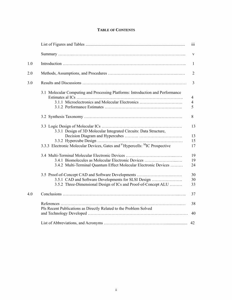
that, in order to ensure the projected microelectronics scaling trends, the cost of facilities to fabricate nanoscale microelectronics may reach hundreds of billion dollars by 2020.
Figure 1. Envisioned molecular (nano) electronics advancements and Moore’s laws for microelectronics Existing superb bimolecular processing / memory platforms and progress in molecular electronics provide evidence of fundamental soundness and technological feasibility for molecular electronics. Some data and expected developments, reported in Figure 1, are subject to adjustments because it is difficult to accurately foresee the fundamental development and maturity of prospective technologies due to the impact of many factors. It may be expected, that by 2025-2030 the core modules of super-high-performance processing (computing) platforms may be implemented using MICs. The emergence of molecular electronics and processing platforms is pervasive and irreversible. However, these high-risk high-payoff areas will require immense research and technology development efforts which largely depend on readiness, commitment, acceptance, investment, infrastructure, innovations and market needs. The dominating premises of molecular (nano) processing and computing have a solid biological association. In fact, there exist a great number of superb molecular systems and platforms that utilize biological molecules. They possess profoundly different processing and memory devices, modules and systems from current electronics systems. Device-level biophysics operations are based on electrochemomechanically-induced transitions, interactions and events, while the system-level fundamentals are expected to rely on integrated processing-and-memory organization and neuromorphological reconfigurable architectures [4]. Real-time 3D image processing is ordinarily accomplished by primitive insects and vertebrates that have less than 1 million neurons. To perform these and other immense processing tasks, less than 1 μW is consumed. However, real-time 3D image processing cannot be performed by even envisioned processors with trillions of transistors, 1 THz device switching speed, 10 GHz circuit speed, 1×10–16 J device switching energy, 1×10–16 J/bit writing energy, and 10 nsec read time. This is evidence of superb biomolecular processing efficiency that cannot be surpassed by any envisioned standard microelectronics enhancements and innovations. Biomolecular processing provides a sound foundation to the overall soundness of envisioned molecular computing and processing platforms.

5
Molecular devices and MICs can operate due to electron or ion transport, photon interaction, biomolecular interactions, transitions, etc. Distinct classes of devices, basic physics, phenomena exhibited, effects utilized and fabrication technologies can be profoundly different. Molecular electronics, theory, engineering practice and technology will require revolutionary advances compared with microelectronics theory and CMOS technology. From a 3D-centered topology, organization, architecture standpoint, solid and fluidic molecular electronics evolution mimics (to some degree) biomolecular solutions. Compared with the most advanced CMOS processors, molecular platforms will greatly enhance functionality and processing capabilities, radically decrease dimensionality, latency, power and execution time, as well as drastically increase device density, utilization and memory capacity. Many difficult problems at the device and system levels must be addressed, researched and solved. Development is required in design, analysis, optimization, aggregation, routing, evaluation, reconfiguration, verification and evaluation. 3.1.2. Performance Estimates. Combinational and memory MICs can be designed as aggregated hypercubes and implemented as ℵhypercells [4, 6, 7]. At the device level, one examines functionality, studies characteristics and estimates performance of 3D-topology MEdevices. The device- and system-level performance measures are of great interest. To analyze the device energetics, examine the switching energy, transit speed, and other baseline characteristics, we applied quantum mechanics [4-7]. Photon Absorption and Transition Energetics − A photon is an emitted or absorbed quantum of electromagnetic energy, and each photon of frequency v (v=c/λ) has an energy E=hv, where h is the Planck constant, h=6.62606876×10⁻³⁴ J-sec, c is the speed of light and λ is the wavelength. Thus, the energy of a single photon is given by E=hc/λ. The maximum absorbance for typical bio-molecule, rhodopsin is 498 nm. For this wavelength, one finds E=4×10⁻¹⁹ J. This energy is sufficient to ensure transitions and functionality. Thus, the energy of a single photon, which is E=4×10⁻¹⁹ J, ensures the functionality of a molecular complex of 348 amino acids composed of ~5000 atoms. We derived the excitation energy (signal energy) which is sufficient to ensure electrochemomechanically-induced state transitions and interactions leading to processing. This provides evidence that ~1×10⁻¹⁹ to 1×10⁻¹⁸ J of energy is required to accomplish the state transitions for molecular aggregates in the biomolecular processing hardware. Energy Levels and Energetics of MEDevices − In MEdevices, one can calculate the energy required to excite an electron and the allowed energy levels can be quantized. The application of quantum mechanics results in the expression for the quantized energy, and for a hydrogen atom:
222
02
4
32 nemE e
nhεπ
−= ,
where me is the electron effective mass, e is the electron charge, εo is the free space permittivity constant, h is the modified Planck constant and n is the principal quantum number. The energy levels depend on the quantum number n. As n increases, the total energy of the quantum state becomes less negative, and En→0 if n→∞. The state of lowest total energy is the most stable state for the electron. The normal state of the electron for a hydrogen (one-electron atom) is at n=1.
The conversion 1 eV=1.602176462×10⁻¹⁹ J is commonly used, and En=1=–2.17×10⁻¹⁸ J=–13.6 eV. For n=2, n=3 and n=4, we have En=2=–5.45×10⁻¹⁹ J, En=3=–2.42×10⁻¹⁹ J and En=4=–1.36×10⁻¹⁹ J. The energy difference between the quantum states n1 and n2 is

6
ΔE=En1–En2, and ⎟⎟⎠
⎞⎜⎜⎝
⎛−=−=Δ 2
122
220
2
4
2111
32 nnemEEE e
nnhεπ
,
where 22
02
4
32 hεπeme =2.17×10⁻¹⁸ J=13.6 eV.
The excitation energy of an exited state n is the energy above the ground state, e.g., for the hydrogen atom one has (En–En=1). The first exited state (n=2) has the excitation energy En=2–En=1=–3.4+13.6=10.2 eV. Using n, one may estimate ΔE deriving the energy required to ensure the quantum transitions and interactions. For many-electron atoms, an atom in its normal (electrically neutral) state has Z electrons and Z protons. Here, Z is the atomic number. For boron, carbon and nitrogen, Z=5, 6 and 7, respectively. By evaluating the average value for the radius of the shell, the effective nuclear charge Zeff is found. The common approximation to calculate the total energy of an electron in the outermost populated shell is
222
02
42
32 neZm
E effen
hεπ−= , and
2
2181017.2
nZ
E effn
−×−= J.
The effective nuclear charge Zeff is found by using the electron configuration. For boron, carbon, nitrogen, silicon and phosphorus, three commonly used Zeff are (Slater, Clementi and Froese-Fischer techniques): 2.6, 2.42 and 2.27 (for B), 3.25, 3.14 and 2.87 (for C), 3.9, 3.83 and 3.46 (for N), 4.13, 4.29 and 4.48 (for Si) and 4.8, 4.89 and 5.28 (for P). Taking note of the electron configurations for the above mentioned atoms (Z/n≈1), one concludes that ΔE is from ~1×10⁻¹⁹ to 1×10⁻¹⁸ J. If one supplies the energy greater than En to the electron, the energy excess will appear as kinetic energy of the free electron. The transition energy should be adequate to excite electrons. For different atoms and molecules with different exited states, as prospective solid MEdevices, the transition (switching) energy is estimated to be ~1×10⁻¹⁹ to 1×10⁻¹⁸ J. This energy estimate is in agreement with biomolecular devices. Device Switching Speed. The transition (switching) speed of MEdevices largely depends on the device physics and phenomena utilized. Considering the electron transport, one may assess the lower bounds for a switching frequency using the number of electrons to ensure on/off switching. For example, for 1 nA current, the number of electrons that cross the molecule per second is 1×10⁻⁹/1.6022×10–
19=6.24×10⁹, and is related to switching capabilities. The maximum carrier velocity places an upper limit on the frequency response of semiconductor devices and MEdevices. Theoretically, the switching can be accomplished by a single electron. Using the Bohr postulates, the average velocity of an optically-exited
electron is n
Zevh0
2
4πε= . Taking note that for all atoms Z/n≈1, one finds the orbital velocity of an optically-
exited electron to be v=2.2×10⁶ m/sec or v/c≈0.01. Taking note of E=mv2/2, we obtain the electron
velocity as a function of energy, e.g., mEEv 2)( = . Letting E=0.1 eV=0.16×10⁻¹⁹ J, one finds v=1.88×10⁵
m/sec. Assuming 1 nm length of the electron path, the traversal time is τ=L/v=5.33×10–15 sec. Hence, MEdevices can operate at high switching frequency. However, one may not conclude that the device switching frequency to be utilized is f=1/τ due to device physics specifics (number of electrons, heating, interference, potential, energy, etc.), system-level functionality, circuit specifications, etc. Reported estimates indicate that the electron velocity in MEdevices exceeds the carrier saturated drift velocity in semiconductors.
7
System Level Processing Performance Estimates. In reporting the performance estimates, we focus on molecular electronics, basic physics and our envisioned solutions. The topology of envisioned molecular devices and systems are analogous to the 3D-centered topology of biomolecular processing platforms. Aggregated brain neurons perform superb information processing, perception, learning, robust reconfigurable networking, memory storage and other functions. The number of neurons in the human brain is estimated to be ~100 billion, while mice and rats have ~100 million neurons. Flies accomplish real-time precisely coordinated motion control with a remarkable actuation and visual system which maps the relative motion using retinal photo-detector arrays. The information from the visual system and sensors is transmitted and processed at the nanoseconds range requiring μW of power. The dimension of the neuron is ~10 µm, and the density of neurons is thousands of neurons in mm3. The biophysics and mechanisms of biomolecular information processing are not fully comprehended. Performing enormous information processing tasks with immense performance (speed, accuracy and robustness) that are far beyond foreseen capabilities of envisioned parallel vector processors (that perform signal and data processing), the human brain consumes only ~20 W. Only some of this power is required to accomplish information and signal/data processing. This contradicts some postulates of slow processing, immense delays, high energy/power requirements, low “switching speed” and other hypotheses. The human retina has 125 million rod cells and 6 million cone cells, and this enormous data stream, among with other tasks, is processed in real-time. As demonstrated above, MEdevices can operate with the estimated required transition energy ~1×10⁻¹⁸ J, discrete energy levels (ensuring multiple-valued logics and memory) and femtosecond transition dynamics promising exceptional device performance [4]. These 3D-topology MEdevices result in the ability to design super-high-performance processing and memory platforms (systems) with novel architectures ensuring unprecedented capabilities including massive parallelism, robustness, reconfigurability, etc. Distinct performance measures, estimates and indexes are used. Figure 2 reports some baseline performance estimates for profoundly different paradigms (microelectronics versus molecular electronics that are distinguished by distinct topologies, organizations and architectures), e.g., transition (switching) energy, delay time, dimension and number of modules/gates. It was emphasized that device physics and system organization/architecture are dominating premises as compared to the dimensionality or number of devices. Due to limited demonstrated experimental results as well as the attempts to use four performance variables, some performance measures and projected estimates reported in Figure 2 are expected to be refined and adjusted in the future. Molecular electronics and MICs can utilize diverse molecular primitives and devices that: (1) Operate due to different physics, for example, electron transport, electrostatic transitions, photon emission, conformational changes, etc.; (2) Exhibit distinct phenomena and effects. Therefore, biomolecular, fluidic, solid and hybrid molecular devices and systems will exhibit distinct performance. As demonstrated in Figure 2, advancements are envisioned towards 3D solid molecular electronics departing from biomolecular processing by utilizing a familiar solid-state microelectronics solution. In Figure 2, 3D-topology neuron operation is represented as a biomolecular information processing and memory module (system).

8
Figure 2. Towards molecular electronics and computing (processing) platforms:
• Revolutionary advancements: From 2D microelectronics to 3D molecular electronics • Evolutionary developments: From biomolecular to solid MEdevices
3. 2. SYNTHESIS TAXONOMY
We developed a novel unified top-down/bottom-up synthesis taxonomy in design of computing and processing platforms. By utilizing this taxonomy, our goal was to perform:
I Top-down Synthesis: We devised novel super-high-performance 3D computing platforms within a 3D fused processing-and-memory organization and a reconfigurable 3D networking-and-processing neuromorphological architecture. Molecular ICs were designed using advanced data structure methods by applying 3D hypercubes, and MICs (molecular processing hardware) were implemented as aggregated ℵhypercells composed from Mgates that are engineered from multi-terminal MEdevices (atomic aggregates), see Figures 3.a and 3.b;
II Bottom-up Synthesis: We synthesized MEdevices from atomic complexes, arranged in functional molecular aggregates that comprise of Mgates within ℵhypercells and ℵhypercells lattices. We implemented the envisioned architectures and organizations by utilizing networked ℵhypercells which form MICs to realize the circuit design.
9
Figure 3. (a) Three-dimensional molecular electronics: Hypercubes Dijk implemented by ℵhypercells
(atomic or molecular aggregates) composed from Mgates that integrate multi-terminal MEdevices engineered from atomic complexes;
(b) Concurrent synthesis and design at system, subsystem and gate (device) levels.
Major Innovations: The modeled 3D3 technology and computing platform utilize five major innovations at the system and device levels to support top-down/bottom-up synthesis:
1. Enabling architectures, organization, topologies, aggregation and networking; 2. Unique phenomena, effects and capabilities (quantum tunneling, parallelism, robustness,
etc.); 3. Novel multi-terminal MEdevices which form Mgates, ℵhypercells and MICs; 4. Nanotechnology: Molecular and organic synthesis as a bottom-up fabrication technology; 5. SLSI as a CAD-supported synthesis, design, analysis and evaluation paradigm. Bottom-Up/Top-Down Synthesis Taxonomy – High-performance computing and processing
platforms can be synthesized using hypercubes Dijk which can be implemented utilizing ℵhypercells. This provides an analogy to the superb 3D biomolecular processing platforms. A coherent synthesis must be performed to accomplish all tasks within the specific flow-map. From the design prospective, 3D molecular synthesis and aggregation are not analogous to the CMOS layout synthesis. Furthermore, VLSI/ULSI design is based on conventional CMOS fabrication technology, 2D (planar) organization, conventional architectures and solid-state gates with FETs and bipolar junction transistors (BJTs). The proposed 3D3 technology utilizes a unified top-down (system level) and bottom-up (device/gate level) synthesis taxonomy within an x-design flow map which is depicted in Figure 4. Thus, the core 3D design themes are integrated within four domains:
• Devising (synthesis) with validation • Modeling–analysis–evaluation
• Design–optimization • Nanotechnology–fabrication

10
Figure 4. Top-down and bottom-up synthesis taxonomy with x-design flow-map.
Data Structure, Decision Diagram, and Hypercubes – For 2D CMOS ICs, the decision diagram (unique canonical structure) is derived as a reduced decision tree by using topological operators. In contrast, for 3D MICs, a new class of decision diagrams and synthesis methods must be developed [4, 10, 11]. We used a novel linear decision diagram which is mapped by 3D hypercubes. This 3D hypercube (cube, pyramid, hexagonal or other 3D topological clusters) uses a unique canonical structure which is a reduced decision tree. Hypercubes were found by using topological operators, e.g., deleting and splitting nodes. Optimal linear decision diagrams were mapped to the 3D hypercubes. By mapping the 3D molecular technology, the hypercube structures ensure synthesis specificity. We modeled optimal topology mapping and suboptimal technology-specific topology mapping of complex switching functions. The major optimization criteria were: (1) minimization of decision diagram nodes and circuit terminals; (2) topological structures (linear arithmetic versus nonlinear arithmetic that leads to simple synthesis and straightforward embedding of linear decision diagrams into 3D topologies); (3) minimization of path length in decision diagrams; (4) simplified routing; (5) minimization of circuit complexity. These criteria resulted in power dissipation reduction, verification simplicity, testability enhancement, as well as other important features. For example, switching power is not only a function of device/gate-realization (BJTs and FETs for CMOS), but also a function of circuit topology, design methods, routing, dynamics, switching activities and other factors that can be optimized thereby reducing the switching power and losses. Neuronal Hypercells – As was emphasized, ℵhypercells are formed by Mgates which are engineered from MEdevices. Performance and characteristics of molecular complexes are drastically affected by the atomic (molecular) structures, aggregation, bonds, atomic orbitals, electron affinity, ionization potential, arrangement, sequence, assembly, folding and other features. We focused our efforts on design of MEdevices, Mgates and ℵhypercells which ensured desired switching (logic) functions, practical electronic characteristics, desired performance, specified geometry (conformation), and functionality. Super-high bandwidth (switching frequency), superior density, low power, low voltage, desired I–V characteristics, enhanced functionality, noise immunity, robustness and other characteristics were ensured through a coherent design. Device performance and characteristics can be changed and optimized by altering and controlling quantum processes, transitions, interactions, etc. For MEdevices, the number of quantum wells, barrier width, energy profile, tunneling length, propagation path, dielectric constant and other features can be adjusted and optimized by designing molecules with controlled atomic sequences, bonds, branches, etc. The goal is to ensure optimal achievable performance and assess it using

11
the performance evaluation metrics. The interactive synthesis taxonomy is integrated with the system-level tasks to be performed as reported in Figure 4. Reconfigurable Networking-and-Processing Neuromorphological Architectures – The neuroarchitectronics paradigm served as the basis for the design of novel super-high-performance molecular computing and processing platforms which are envisioned to be implemented utilizing 3D-topology MICs. The networked neuronal aggregates were prototyped by ℵhypercell lattices, which ensure a fused processing-and-memory organization, while reconfigurable networking-and-processing neuromorphological architecture was ensured due to inherent 3D-topology, enabling performance, enhanced capabilities (routing, networking, etc.) and other advantages of the 3D3 technology. For example, the modular ℵhypercell can implement the switching function of arbitrary complexity (performing multiple-valued combinational logics and processing) as well as store data. Figure 5 illustrates the organization and architecture of the computing and memory platforms.
Figure 5. Processing and memory platforms: Fused processing-and-memory organization and
reconfigurable networking-and-processing neuromorphological architecture Reconfigurable computing is an established term that applies to any device or primitive which can be configured, at run-time, to implement a function utilizing a specific hardware solution. A reconfigurable device should possess adequate logic, reprogramming and routing capabilities to ensure reconfiguration features, as well as to compute a large set of functions. The reconfigured MEdevice performs a different set of functions. Consider a Mgate with binary inputs A and B. Using the outputs to be generated by the universal logic gate, one has the following 16 functions: 0, 1, A, B, A , B , A+B,
BA + . BA + , BA + , AB, BA , BA , BA , BABA + and BAAB + . The standard logic primitives (AND, NAND, NOT, OR, NOR and other) can be implemented using a Fredkin gate which performs conditional permutations. Consider a Mgate with a switched input A and a control input B. As illustrated in Figure 6, the input A is routed to one of two outputs, conditional on the state of B. The routing events change the output switching function which is AB or BA .
A
BBA
AB
B
Figure 6. Molecular gate schematic

12
Utilizing the proposed molecular processing paradigm, routable molecular universal logic gates can be designed and implemented using neuromorphological architectures. We defined a routable molecular universal logic gate as a reconfigurable combinational gate that can be reconfigured to realize specified functions of its input variables. These routable molecular universal logic gates can realize logic functions using multi-input variables with the same delay as a two-input Mgate. Logic functions can be efficiently factored and decomposed. Figure 7 schematically depicts the proposed routing concepts for reconfigurable logic [4]. The typified 3D-topologically reconfigurable routing is accomplished through the connecting/disconnecting of Mgates which perform processing and memory storage. For illustrative purposes, Figure 7 demonstrates reconfiguration of 5 Mgates within 10 ℵhypercells depicting a reconfigurable networking-and-processing in 3D. The inputs are denoted as x1, x2, x3, x4, x5 and x6. The use of reconfigurable routing uniquely enhances and complements the capabilities of the ℵhypercell solution. In general, one may not be able to route just any output of any gate/hypercell/module to just any input of any other gate/hypercell/module. There are synthesis constraints, selectivity limits, complexity to control the spatial motion of electrons as the routers, as well as other limits which should be integrated in the design.
x2
x3x4
x5
x6
x2
x3x4
x5
x6
x2
x3
x4
x5
x6
x1x1x1
Figure 7. Reconfigurable routing and networking
Utilizing molecular electronics, one can control charged carriers (electrons) and steer electrons in 3D accomplishing directed routing and adaptive spatial networking. We modeled the processing and routing transition functions Fp and Fr which describe previous processing and routing states to the resulting new states in [t, t+], t+>t. The output evolution is given as y(t+)=Fi[t,x(t),y(t),u(t)], where x and u are the state and control vectors. For example, u leads to the routing control with the resulting routing and reconfigurable networking. The reconfiguration is described as P⊂X×Y×U, where X, Y and U are the input, output and control sets. Design Rules – MICs can be synthesized through hierarchical synthesis motifs utilizing ℵhypercells as molecular hardware primitives [4]. One may envision 3D directly interconnected molecular electronics utilizing a direct device-to-device aggregation. The MEdevice-MEdevice interconnect can be accomplished as the chemical-bonding fabric (atomic bonding), and be energy-based (for example, utilizing the exchange/conversion/transmission of radiated and absorbed electromagnetic energy), etc. We designed reconfigurable MICs and developed complimentary software tools to cope with non perfect (partially defective and faulty) ℵhypercells and circuits in arithmetic, control, input-output, memory and other functions. Molecular electronics will result in MICs with a significant number of entirely or partially defective and faulty devices and interconnects [4]. Reconfiguration along with redundancy ensures overall soundness. The circuit reconfigurability capability is determined by the yield, complexity, software abilities (to detect, identify and tolerate the hardware deficiencies), etc. Adaptability and
13
reconfigurability can be achieved through hardware diagnostics, testing and analysis with the following mapping, matching, switching, controlling, rerouting and networking tasks performed by software [4]. In general, one designs, optimizes, builds, tests/evaluates and reconfigures MICs. We developed the following design rules:
1. Design and optimize MICs performing SLSI design; 2. Apply the target MICs realization using the modular ℵhypercells; 3. Design a specific ℵhypercell template assessing the expected yield and error rates; 4. Analyze and perform the bottom-up synthesis developing and specifying the technology,
processes and other tasks to synthesize MICs as an assembly of ℵhypercell aggregates; 5. Utilizing hierarchical
• (i) random circuit assembly with random sequences, (ii) near-random assembly with near-random sequences, or (iii) ordered assembly with deterministic sequences,
• specificity (terminal/interconnect-recognition, terminal/interconnect site recognition, self-binding, paring and complimentary compliance of ℵhypercells within node lattices),
• nearest-neighboring ℵhypercell placement motifs, synthesize ℵhypercell aggregates forming node lattices which should realize MICs;
6. Perform hardware/software-centered diagnostics, verification and testing; 7. Reconfigure, characterize, evaluate and validate MICs.
These design rules define the random, near-random or ordered (directed) ordering of ℵhypercells and their aggregates. Using this hierarchical strategy, one ensures the soundness of the integrated design-synthesis-networking-and-reconfiguration tasks. This sub-optimal solution promises to ensure:
1. Affordability and high yield with potentially tolerable error rate; 2. Selectivity and specificity of ℵhypercells as processing and memory primitives; 3. Controllable self-assembling and robust binding/paring by utilizing ℵhypercell-ℵhypercell and
ℵhypercell-interconnect uniformity, complimentary compliance and recognition; 4. Overall functionality.
3. 3. LOGIC DESIGN OF MOLECULAR ICS
3.3.1. Design of 3D Molecular Integrated Circuits: Data Structure, Decision Diagram and Hypercubes
The dimension of a decision diagram (number of nodes) is a function of the number of variables and the variables ordering. In general, the design complexity is O(n3). This complexity significantly limits the design capabilities in terms of IC complexity (number of gates) for which the design can be performed. The commonly utilized word-level decision diagrams further increase complexity due to processing of data in word-level format. Therefore, novel concepts are needed. We devised a sound software-supported design approach which features SLSI capabilities. In particular, novel methods in data structure representation and data structure manipulation were developed and demonstrated by the Microsystems and Nanotechnologies team to ensure design specifications and objectives. We applied linear word-level decision diagrams (LWDDs) accomplishing compact representation of logic circuits using linear arithmetical polynomials [10, 11]. The design complexity becomes O(n). The concept ensures compact representation of circuits compared with other formats and methods. The design algorithm is: Function (Circuit) ↔ BDD Model ↔ LWDD Model ↔ Hypercube Realization ↔ MICs Implementation (ℵHypercell Lattice) where BDD is a Binary Decision Diagram.
14
The hypercube we utilized is a homogeneous aggregated assembly for massive super-high-performance parallel computing. Switching theory was applied to design the 3D hypercubes. To perform logic design, graph-based data structures in 3D space were utilized [11]. The hypercube is a topological representation of a switching function by n-dimensional graph. The switching function f is given as:
( ) Function Switching of Form...12
0Function Switching 1
1
tCoefficien
Operation
⇒−
=⇒ Ω
⇓
⇑
nin
i
n
xxiiL
The data structure is described in matrix form using the truth vector F of a given switching function f as well as the vector of coefficients Ω. The logic operations are represented by L. The logic design in spatial dimensions is based on advanced methods and data structures in 3D. For hypercubes, the appropriate data structure of logic function and methods of embedding this structure in hypercubes must be found. We developed a three-step-solution in logic function manipulation to change the carrier of information from the algebraic form (logic equation) to the hypercube structure. In particular:
Step 1: Logic function is transformed to the appropriate algebraic form (Reed-Muller, arithmetic or word-level in matrix or algebraic representation);
Step 2: Derived algebraic form is converted to the graphical form (decision tree, decision diagram or logic network);
Step 3: Obtained graphical form is embedded into hypercube. Hence, the design is expressed as:
3 Step2 Step1 StepStructure Hypercube- GraphFunction Logic N⇔⇔ .
The linear word-level decision diagram (LWDD) allows one to perform the compact representation of logical circuits utilizing linear arithmetic polynomials (LPs). This approach ensures compact representation of circuits compared with other formats. The algorithm is given as Function (Circuit) ↔ BDD Model ↔ LWDD Model ↔ Hypercube Realization ↔ MICs Implementation (ℵHypercell Lattice). The LWDD is imbedded in hypercubes resulting in circuits in a 3D space. The polynomial representation of logical functions ensures the description of a many-output function in a word-level format. The expression of a Boolean function f of n variables (x1, x2, … xn-1, xn) is
∑=
−− +=+++++=n
jjjnnnn xaaxaxaxaxaaLP
101122110 ... .
The resulting mapping establishes LWDD (a0,a1,a2,…,an-1,an) ↔ LP. The nodes of LP correspond to a positive Davio expansion. Thus, LWDDs are obtained by mapping LPs where the nodes correspond to the positive Davio expansion, and functionalizing vertices related to the coefficients of the LPs. The LWDD design flow is: Primitive↔LP Model↔LWDD Model↔ Realization. The proposed LWDDs uniquely complement our 3D3 technology ensuring large-scale data manipulation and SLSI design capabilities. Our LWDDs can be used to perform logic design and circuitry mapping utilizing hardware description languages. For different ICs, we performed a proof-of-concept logic design using the concept reported. The goal was to perform the design and evaluate it by examining the number of nodes (N), number of levels, CPU time required to design decision diagrams, etc. Topological characteristics were evaluated using the volumistic quantity, total number of terminals,
15
number of intermediate nodes and other parameters as reported in section 3.5.2, see Tables 1 and 2. Time and memory complexity is linearly upper-bounded by O(n) with respect to number of gates, while the conventional methods result in complexity O(n3). The concept results in:
1 Coherent algebraic representation of manipulation of complex switching functions; 2 Tractable matrix representation and manipulations; 3 Graph-based representation, as found using decision trees, decision diagrams and logic
networks; 4 Data structures embedded into hypercubes.
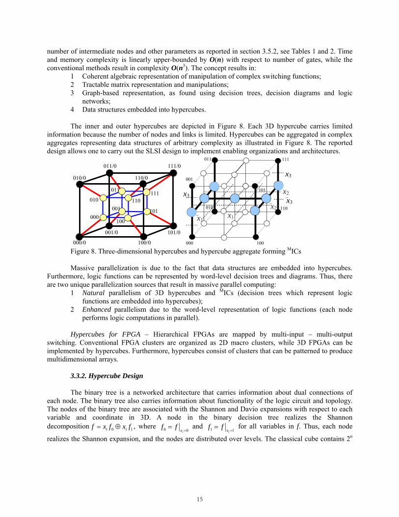
The inner and outer hypercubes are depicted in Figure 8. Each 3D hypercube carries limited information because the number of nodes and links is limited. Hypercubes can be aggregated in complex aggregates representing data structures of arbitrary complexity as illustrated in Figure 8. The reported design allows one to carry out the SLSI design to implement enabling organizations and architectures.
000100
010 110
011 111
101
101/0
111/0
100/0000/0
001/0
110/00
011/0
010/00
001x1
x3x2
x3
⎯x3
⎯x1
⎯x2
000 100
110
111
001
011
010
101
Figure 8. Three-dimensional hypercubes and hypercube aggregate forming MICs Massive parallelization is due to the fact that data structures are embedded into hypercubes. Furthermore, logic functions can be represented by word-level decision trees and diagrams. Thus, there are two unique parallelization sources that result in massive parallel computing:
1 Natural parallelism of 3D hypercubes and MICs (decision trees which represent logic functions are embedded into hypercubes);
2 Enhanced parallelism due to the word-level representation of logic functions (each node performs logic computations in parallel).
Hypercubes for FPGA – Hierarchical FPGAs are mapped by multi-input – multi-output switching. Conventional FPGA clusters are organized as 2D macro clusters, while 3D FPGAs can be implemented by hypercubes. Furthermore, hypercubes consist of clusters that can be patterned to produce multidimensional arrays. 3.3.2. Hypercube Design The binary tree is a networked architecture that carries information about dual connections of each node. The binary tree also carries information about functionality of the logic circuit and topology. The nodes of the binary tree are associated with the Shannon and Davio expansions with respect to each variable and coordinate in 3D. A node in the binary decision tree realizes the Shannon decomposition 10 fxfxf ii ⊕= , where
00 ==
ixff and
11 ==
ixff for all variables in f. Thus, each node
realizes the Shannon expansion, and the nodes are distributed over levels. The classical cube contains 2n
16
nodes, while the hypercube has ∑=
−+n
i
mi
nn C0
122 nodes in order to ensure a technology-specific design of
MICs. The hypercube consists of terminal nodes, intermediate nodes and roots. The most straightforward implementation is provided by using molecular multiplexers (MMUX). However, other Mgates can be utilized as well. The design steps are: Step 1: Connect the terminal node with the intermediate nodes; Step 2: Connect the root with two intermediate nodes located symmetrically on the opposite faces; Step 3: Pattern the terminal and intermediate nodes on the opposite faces and connect them via the root. There are several methods for representing logic functions. A hypercube, proposed as a core solution, is a homogeneous aggregated assembly for massive super-high-performance parallel computing. We applied enhanced switching theory integrated with a novel logic design concept [11]. In the design, the graph-based data structures and 3D circuit topology were utilized. The hypercube is a topological representation of a switching function by an n-dimensional graph. In particular, the switching function f is given as
( ) ....12
0
Function Switching of Form
1
tCoefficien
Operation
Function Switching1
Fin
i
n
fxxii
f n ⇒−
=⇒
⇓
⇑
KL
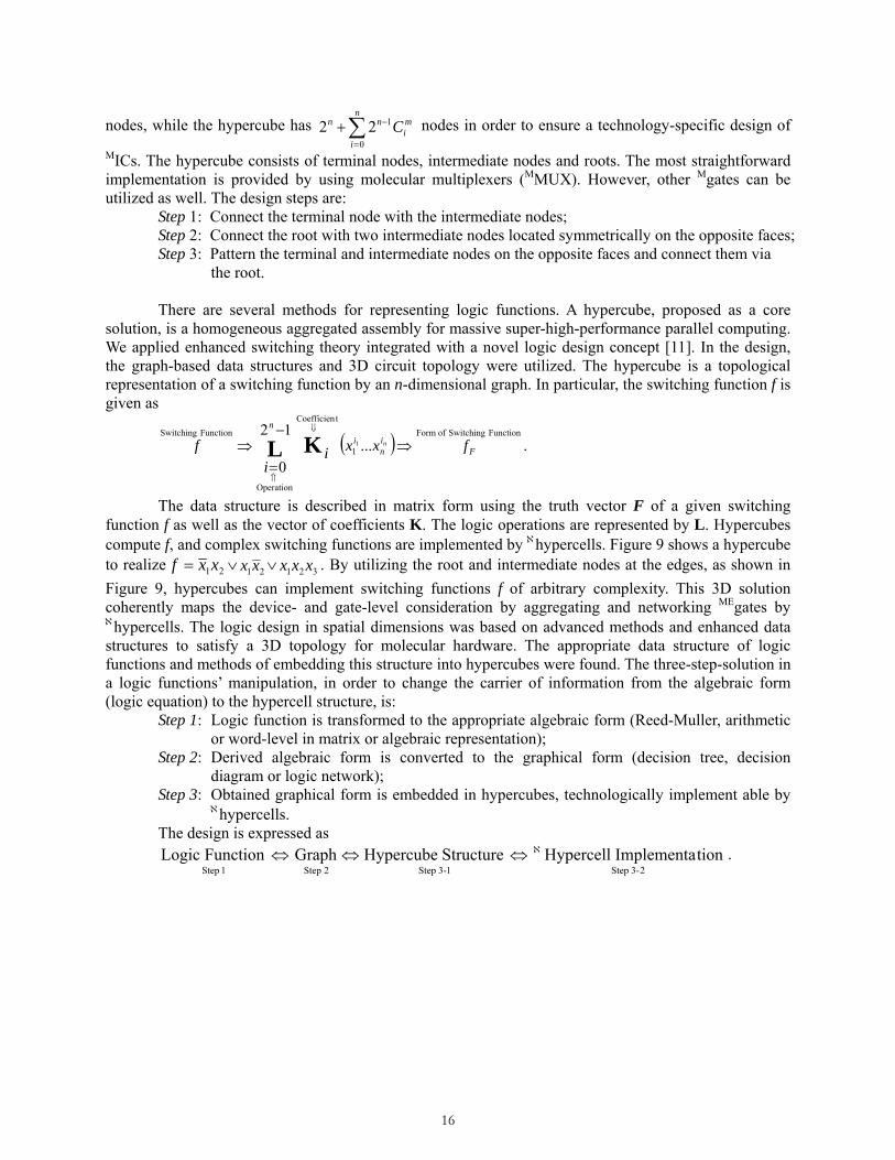
The data structure is described in matrix form using the truth vector F of a given switching function f as well as the vector of coefficients K. The logic operations are represented by L. Hypercubes compute f, and complex switching functions are implemented by ℵhypercells. Figure 9 shows a hypercube to realize 21xxf = ∨ 21xx ∨ 321 xxx . By utilizing the root and intermediate nodes at the edges, as shown in Figure 9, hypercubes can implement switching functions f of arbitrary complexity. This 3D solution coherently maps the device- and gate-level consideration by aggregating and networking MEgates by ℵhypercells. The logic design in spatial dimensions was based on advanced methods and enhanced data structures to satisfy a 3D topology for molecular hardware. The appropriate data structure of logic functions and methods of embedding this structure into hypercubes were found. The three-step-solution in a logic functions’ manipulation, in order to change the carrier of information from the algebraic form (logic equation) to the hypercell structure, is:
Step 1: Logic function is transformed to the appropriate algebraic form (Reed-Muller, arithmetic or word-level in matrix or algebraic representation);
Step 2: Derived algebraic form is converted to the graphical form (decision tree, decision diagram or logic network);
Step 3: Obtained graphical form is embedded in hypercubes, technologically implement able by ℵhypercells.
The design is expressed as
23- Step13- Step2 Step1 SteptionImplementa Hypercell Structure Hypercube GraphFunction Logic ℵ⇔⇔⇔ .

17
011 111
101
100000
010
001
110
1x 1x3x
3x
3x
3x 3x
2x
2x
3x
3x 3x
2x
2x
100000
010 110
1x
3x3x
3x 3x
2x
001
1x 1x3x
3x
3x
3x 3x
2x
2x
3x
3x 3x
2x
2x
Subcube
Figure 9. Hypercube which implements function f
The proposed concept results in: 1. Algebraic representation and robust rules of manipulation for complex switching logic functions; 2. Matrix representation and sound manipulation; 3. Consistency of logic relationships for variables and functions from the spectral theory viewpoint
due to the use of matrix algebra; 4. Graph-based representation is found using decision trees, decision diagrams and logical networks; 5. Data structures are embedded into hypercubes.
3.3.3. Electronic Molecular Devices, Gates and ℵHypercells: MIC Prospective In VLSI design, resistor-transistor logic, diode-transistor logic, transistor-transistor logic, emitter-coupled logic and other logic families have been used. All logic families and subfamilies have advantages and drawbacks, (within transistor-transistor logic, there are Schottky, low-power Schottky, advanced Schottky and others). In molecular electronics, one cannot adapt or utilize VLSI/CMOS-based design due to distinct fabrication technologies, topologies/organization/architectures, design rules, etc. This subsection focuses on some notional molecular device and system level features. Molecular electronic devices offer significant advantages compared with microelectronic devices. For example, quantum effects result in multiple-valued I–V characteristics with very low current even at the maximum potential. This reduces power losses, enhances robustness, provides noise immunity, etc. Correspondingly, some logic families that are marginal in microelectronics may provide superior performance in molecular electronics. The molecular NOR (MNOR) gate, realized using molecular resistor-device logic, is illustrated in Figure 10.a. In electronics, NAND is one of the most important gates. The molecular NAND (MNAND) gate, designed by applying molecular diode-device logic, is shown in Figure 10.b. Molecular electronic devices operate utilizing phenomena and effects different compared with microelectronic devices, therefore in Figures 10.a and 10.b, we use different symbols to
designate molecular resistors (MEr), diodes (MEd), and multi-terminal devices (MED).

18
x y
V
yxf +=
xy yxf +=
V
xy
xyf =
x
y
xyf =
MNOR MNAND
MErMEr
MErMErMEr
MEd
MEd
MEd
MED
(a) (b) Figure 10. Circuit schematics of two-input MNOR and MNAND gates The design is accomplished in 3D space using hypercubes, and the designed circuits are implemented by ℵhypercells. An example of a 3D ℵhypercell to implement a logic function f is shown in Figure 11.a. Molecular multi-terminal devices , with six or less inputs and outputs, are the corner
nodes. Two-terminal devices (MEdiodes and MEresistors ) are shown. The input signals x1, x2 and x3, as well as the output switching function f, are documented. Three-dimensional aggregation and topology can be viewed to be biomimetics-centered. Molecular electronic devices and ℵhypercells can be synthesized using engineered polypeptides, e.g., [–N–C–C–]n chains with side groups Si. The implementation of a single ℵhypercell utilizing engineered polypeptides is reported in Figure 11.b. Here, (–N–C–C–)n chains provide the structural skeleton (mechanical structure), while side groups Si provide electron transport. Hence, Si integrate MEdevices engineered from organic molecules as reported in subsection 3.4.2. Figures 11.b and 11.c show how the 3D-topology interconnect is accomplished by Si. ℵHypercells can be clustered and aggregated to form macrocell ℵhypercell aggregates, thereby forming MICs.
f(x1, x2, x3)
Two-Terminal Devices and
Multi-Terminal Device
x1
x2
x3
f(x1,x3)
f(x1,x2,x3)
x1
x2
x3
CCN
OH
=
S
Polypeptide Backbone With Interconnected Side
GroupsS
–N–C–C–
S
–N–C–C–
Organic Molecule With Side Group M011
M01
1
M111
M010M11
0
M000M10
0
M101M00
1
(a) (b) (c) Figure 11. (a) ℵHypercell schematics with two- and multi-terminal MEdevices; (b) Implementation of the ℵhypercell utilizing polypeptides with interconnected side R groups; (c) Implementation of the ℵhypercell by Mijk with eight side groups Sijk.

19
The MNAND gate, which is one of the most important gates, can be implemented utilizing molecular diode-device logic. The resulting ℵhypercell schematic is documented in Figure 12. Molecular gates can be designed from an electronics and quantum mechanics viewpoint, and then synthesized using molecular nanotechnology which is based on organic synthesis. The design and analysis should be performed in order to optimize device characteristics, functionality, aggregate ability, gate topology, circuitry organization, and other features.
V
x
y
xyf =
xy
xyf =
MNAND
x
y
M011
xyf =
V
Figure 12. MGate (MNAND) mapped by a single ℵhypercell and its implementation.
3. 4. MULTI-TERMINAL MOLECULAR ELECTRONIC DEVICE 3.4.1. Biomolecules as Molecular Electronic Devices Sequence-dependent self-assembled DNA and templated protein synthesis can be used to build patterned two- and three-dimensional structures with the desired geometrical topologies [12, 13]. Biomolecules accomplish information processing and memory storage through interactions that are not fully understood, however it is highly unlikely that processing is performed due to effects directly associated with electron flow. Therefore, biomolecular processing hardware does not possess MEdevices or any their equivalents [4]. Some inorganic, organic and hybrid molecules, which exhibit desired electronic properties, are envisioned to be utilized in a new generation of MEdevices in MICs [2-7, 14-20]. Processing, computing and memory platforms are envisioned to be designed and fabricated using self-assembled molecules utilized as multi-terminal MEdevices. The design rules were reported in section 3.2. It is important to design and analyze functional high-performance MEdevices which possess the desired electronic characteristics forming ℵhypercells. Biomolecules have been examined as MEdevices in [21-24]. Contradicting conclusions and obscure results have been reported. Insulating, conducting and semiconducting properties were reported in the contact–biomolecule–contact and inter-biomolecular complexes [21-24]. Biomolecule synthesis, sequence, length, environment, alignment and other factors influence the electronic characteristics. In DNA, various experiments to examine the electron transport, I–V characteristics, conductance and other electronic properties were performed in [21-24] with limited success and contradicting results. Figure 13.a illustrates DNA attached to two electrodes. The electrode electrochemical potentials are denoted as VFs and VFd, while Es and Ed are the self-energy functions of the “source” and “drain” as one uses the FET

20
terminology. Electrochemical potentials VFs and VFd vary. There is no electron transport if the system is in equilibrium, e.g., at VFs=VFd. The highest occupied molecular orbitals (HOMO) and lowest unoccupied molecular orbitals, (LUMO), as well as the Fermi level, are illustrated. Depending on the HOMO and LUMO levels, as well as EF, the electron transport takes place through particular orbitals. Using broadening energies EBs and EBd, the electron flow rates are EBs/h and EBd/h. Guanine quartets (tubular sequences of G tetramers) were reported [22, 23]. Tetramers (G4) are the building blocks of a quadruple-helix forming G4-DNA. The hydrogen-bonded guanines arrange in a 2.3 nm diameter configuration. The prospective G4-DNA-based multi-terminal electronic device can be visualized as shown in Figure 13.b. Though G4-DNA aggregates were synthesized, the electronic characteristics have not been examined due to unsolved interconnect, manipulation and characterization engineering. Two- and multi-terminal DNA-centered devices, reported in Figures 13.a and 13.b, have a limited overall feasibility and soundness from both technological and fundamental standpoints.
Figure 13. a) Double-stranded DNA with two electrodes; b) G4-DNA complex as a possible MEdevice In devising emerging fabrication technologies, one may focus on robust bottom-up biomolecular assembling which is consistently performed by biosystems. Progress has been made in the synthesis of DNA with specified sequences. Utilizing a motif-based DNA self-assembly, complex 3D structures were synthesized [12, 13]. There are precise binding rules, e.g., adenine A with complementary thymine T and guanine G, with complementary cytosine C. Designs to minimize sequence mismatches is a complex task. The desired assemblies frequently cannot be synthesized due to geometric, thermodynamic and other limits of DNA hybridization [12, 13]. Most importantly, experimental results [21-24] provide evidence that DNA and DNA-derivatives do not exhibit the suitable electronic characteristics even for two-terminal rectifiers, and it is unlikely that suitable device functionality may be achieved. Though the 3D multi-interconnected DNA structures can be synthesized, it seems that it is unreasonable to expect sound DNA-centered electronic devices. The resistor-diode logic is covered in subsection 3.3.3. Although the simple resistor-diode circuits can be theoretically assembled using the DNA motif, this solution may be impractical. The metallization of 3D DNA lattices, which enables electron transport in the metallized segments, cannot be viewed as a sound solution for semiconductor operations. DNA with the appropriate sequence potentially can be used only as a biomolecular-centered wire. The qualitative achievable I–V characteristics for the admissible applied voltage for DNA are reported in Figure 14. The magnitude of the applied voltage is bounded due to the thermal stability of the molecule, e.g., |V|≤Vmax, and Vmax is ~1 V depending upon sequence, single versus double stranded, number of base pairs, temperature, functionalization, end-group, etc. For different DNA sequences, the I–V characteristics vary [21], and for the conducting DNA, the characteristics are similar to some organic molecules [2, 4, 14-20]. The asymmetry of the I–V characteristics could be due to the effects related to asymmetric DNA functionalization to the electrodes, contact non-uniformity, or other effects. Three different short (~5.4 nm) double-stranded DNA (dsDNA) sequences, functionalized using short oligonucleotide linkers and
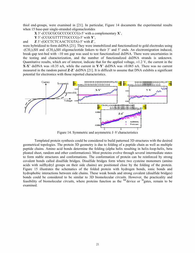
21
thiol end-groups, were examined in [21]. In particular, Figure 14 documents the experimental results when 15 base-pair single-stranded oligonucleotides
X 3’-(CCGCGCGCCCGCCCG)-5’ with a complementary X’, Y 3’-(CCGCGTTTTTGCCCG)-5’ with Y’,
and Z 3’-(GCCTCTCAACTCGTA)-5’ with Z’, were hybridized to form dsDNA [21]. They were immobilized and functionalized to gold electrodes using -(CH2)3SH and -(CH2)6SH oligonucleotide linkers to their 3’ and 5’ ends. An electromigration induced, break-gap test-bed with ~10 nm gap was used to test functionalized dsDNA. There were uncertainties in the testing and characterization, and the number of functionalized dsDNA strands is unknown. Quantitative results, which are of interest, indicate that for the applied voltage, ±1.2 V, the current in the X-X’ dsDNA was ±0.35 nA, while the current in Y-Y’ dsDNA was ±0.065 nA. There was no current measured in the random paired Z-Z’ dsDNA [21]. It is difficult to assume that DNA exhibits a significant potential for electronics with those reported characteristics.
Figure 14. Symmetric and asymmetric I–V characteristics
Templated protein synthesis could be considered to build patterned 3D structures with the desired geometrical topologies. The protein 3D geometry is due to folding of a peptide chain as well as multiple peptide chains. Amino acid bonds determine the folding (alpha helix resulting in helix-loop-helix, beta pleated sheet, random and other conformations). Most proteins evolve through several intermediate states to form stable structures and conformations. The conformation of protein can be reinforced by strong covalent bonds called disulfide bridges. Disulfide bridges form where two cysteine monomers (amino acids with sulfhydryl groups on their side chains) are positioned close by the folding of the protein. Figure 15 illustrates the schematics of the folded protein with hydrogen bonds, ionic bonds and hydrophobic interactions between side chains. These weak bonds and strong covalent (disulfide bridges) bonds could be considered to be similar to 3D biomolecular circuits. However, the practicality and feasibility of biomolecular circuits, where proteins function as the MEdevice or Mgates, remain to be examined.
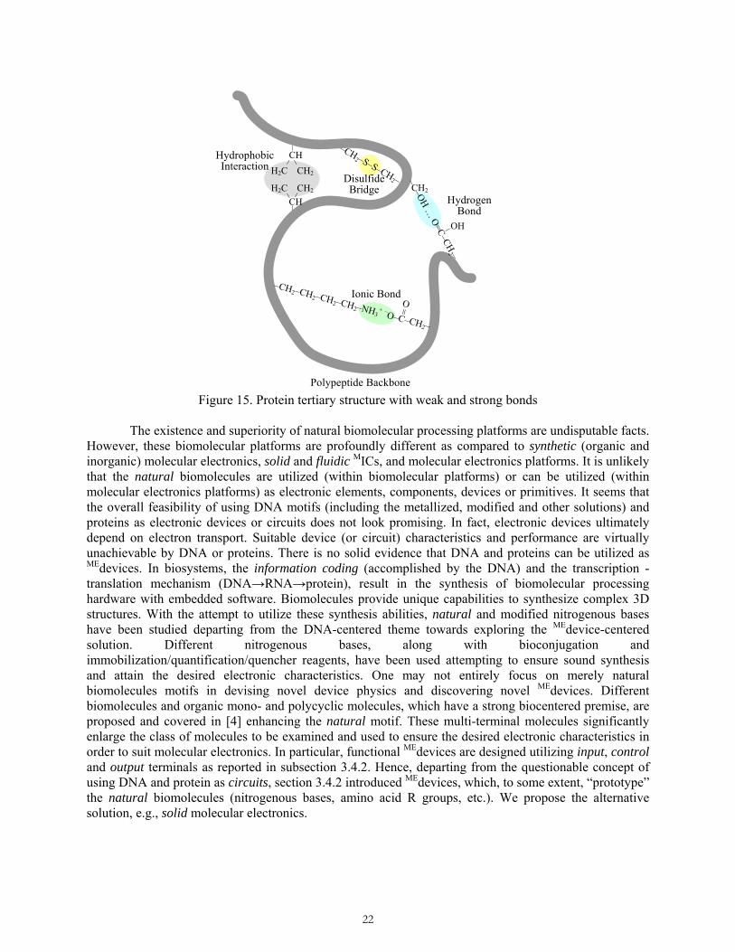
22
–CH2–S–S–CH
2–Disulfide Bridge
–CH2–CH2–CH2–CH2–NH3+ –O–C–CH2–
Ionic Bond
=O
– –OH … O=C–CH
2 –
Hydrogen Bond
OH–
CH2H2C CH2
H2C CH2
CH
CH
–––
––
–
Hydrophobic Interaction
Polypeptide Backbone Figure 15. Protein tertiary structure with weak and strong bonds
The existence and superiority of natural biomolecular processing platforms are undisputable facts. However, these biomolecular platforms are profoundly different as compared to synthetic (organic and inorganic) molecular electronics, solid and fluidic MICs, and molecular electronics platforms. It is unlikely that the natural biomolecules are utilized (within biomolecular platforms) or can be utilized (within molecular electronics platforms) as electronic elements, components, devices or primitives. It seems that the overall feasibility of using DNA motifs (including the metallized, modified and other solutions) and proteins as electronic devices or circuits does not look promising. In fact, electronic devices ultimately depend on electron transport. Suitable device (or circuit) characteristics and performance are virtually unachievable by DNA or proteins. There is no solid evidence that DNA and proteins can be utilized as MEdevices. In biosystems, the information coding (accomplished by the DNA) and the transcription - translation mechanism (DNA→RNA→protein), result in the synthesis of biomolecular processing hardware with embedded software. Biomolecules provide unique capabilities to synthesize complex 3D structures. With the attempt to utilize these synthesis abilities, natural and modified nitrogenous bases have been studied departing from the DNA-centered theme towards exploring the MEdevice-centered solution. Different nitrogenous bases, along with bioconjugation and immobilization/quantification/quencher reagents, have been used attempting to ensure sound synthesis and attain the desired electronic characteristics. One may not entirely focus on merely natural biomolecules motifs in devising novel device physics and discovering novel MEdevices. Different biomolecules and organic mono- and polycyclic molecules, which have a strong biocentered premise, are proposed and covered in [4] enhancing the natural motif. These multi-terminal molecules significantly enlarge the class of molecules to be examined and used to ensure the desired electronic characteristics in order to suit molecular electronics. In particular, functional MEdevices are designed utilizing input, control and output terminals as reported in subsection 3.4.2. Hence, departing from the questionable concept of using DNA and protein as circuits, section 3.4.2 introduced MEdevices, which, to some extent, “prototype” the natural biomolecules (nitrogenous bases, amino acid R groups, etc.). We propose the alternative solution, e.g., solid molecular electronics.
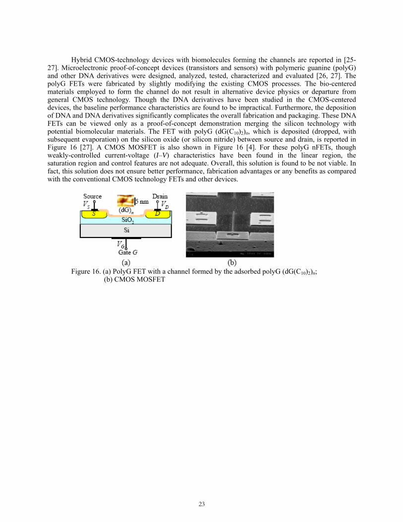
23
Hybrid CMOS-technology devices with biomolecules forming the channels are reported in [25-27]. Microelectronic proof-of-concept devices (transistors and sensors) with polymeric guanine (polyG) and other DNA derivatives were designed, analyzed, tested, characterized and evaluated [26, 27]. The polyG FETs were fabricated by slightly modifying the existing CMOS processes. The bio-centered materials employed to form the channel do not result in alternative device physics or departure from general CMOS technology. Though the DNA derivatives have been studied in the CMOS-centered devices, the baseline performance characteristics are found to be impractical. Furthermore, the deposition of DNA and DNA derivatives significantly complicates the overall fabrication and packaging. These DNA FETs can be viewed only as a proof-of-concept demonstration merging the silicon technology with potential biomolecular materials. The FET with polyG (dG(C10)2)n, which is deposited (dropped, with subsequent evaporation) on the silicon oxide (or silicon nitride) between source and drain, is reported in Figure 16 [27]. A CMOS MOSFET is also shown in Figure 16 [4]. For these polyG nFETs, though weakly-controlled current-voltage (I–V) characteristics have been found in the linear region, the saturation region and control features are not adequate. Overall, this solution is found to be not viable. In fact, this solution does not ensure better performance, fabrication advantages or any benefits as compared with the conventional CMOS technology FETs and other devices.
Figure 16. (a) PolyG FET with a channel formed by the adsorbed polyG (dG(C10)2)n; (b) CMOS MOSFET
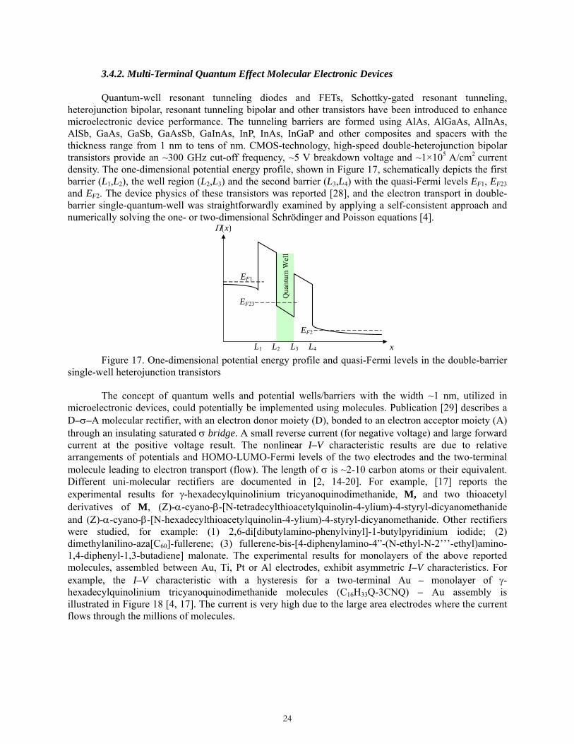
24
3.4.2. Multi-Terminal Quantum Effect Molecular Electronic Devices Quantum-well resonant tunneling diodes and FETs, Schottky-gated resonant tunneling, heterojunction bipolar, resonant tunneling bipolar and other transistors have been introduced to enhance microelectronic device performance. The tunneling barriers are formed using AlAs, AlGaAs, AlInAs, AlSb, GaAs, GaSb, GaAsSb, GaInAs, InP, InAs, InGaP and other composites and spacers with the thickness range from 1 nm to tens of nm. CMOS-technology, high-speed double-heterojunction bipolar transistors provide an ~300 GHz cut-off frequency, ~5 V breakdown voltage and ~1×10⁵ A/cm2 current density. The one-dimensional potential energy profile, shown in Figure 17, schematically depicts the first barrier (L1,L2), the well region (L2,L3) and the second barrier (L3,L4) with the quasi-Fermi levels EF1, EF23 and EF2. The device physics of these transistors was reported [28], and the electron transport in double-barrier single-quantum-well was straightforwardly examined by applying a self-consistent approach and numerically solving the one- or two-dimensional Schrödinger and Poisson equations [4].
xL1
Π(x)
L2 L3 L4
EF1
EF23
EF2
Qua
ntum
Wel
l
Figure 17. One-dimensional potential energy profile and quasi-Fermi levels in the double-barrier
single-well heterojunction transistors The concept of quantum wells and potential wells/barriers with the width ~1 nm, utilized in microelectronic devices, could potentially be implemented using molecules. Publication [29] describes a D–σ–A molecular rectifier, with an electron donor moiety (D), bonded to an electron acceptor moiety (A) through an insulating saturated σ bridge. A small reverse current (for negative voltage) and large forward current at the positive voltage result. The nonlinear I–V characteristic results are due to relative arrangements of potentials and HOMO-LUMO-Fermi levels of the two electrodes and the two-terminal molecule leading to electron transport (flow). The length of σ is ~2-10 carbon atoms or their equivalent. Different uni-molecular rectifiers are documented in [2, 14-20]. For example, [17] reports the experimental results for γ-hexadecylquinolinium tricyanoquinodimethanide, M, and two thioacetyl derivatives of M, (Z)-α-cyano-β-[N-tetradecylthioacetylquinolin-4-ylium)-4-styryl-dicyanomethanide and (Z)-α-cyano-β-[N-hexadecylthioacetylquinolin-4-ylium)-4-styryl-dicyanomethanide. Other rectifiers were studied, for example: (1) 2,6-di[dibutylamino-phenylvinyl]-1-butylpyridinium iodide; (2) dimethylanilino-aza[C60]-fullerene; (3) fullerene-bis-[4-diphenylamino-4”-(N-ethyl-N-2’’’-ethyl)amino-1,4-diphenyl-1,3-butadiene] malonate. The experimental results for monolayers of the above reported molecules, assembled between Au, Ti, Pt or Al electrodes, exhibit asymmetric I–V characteristics. For example, the I–V characteristic with a hysteresis for a two-terminal Au – monolayer of γ-hexadecylquinolinium tricyanoquinodimethanide molecules (C16H33Q-3CNQ) – Au assembly is illustrated in Figure 18 [4, 17]. The current is very high due to the large area electrodes where the current flows through the millions of molecules.

25
I–V Characteristic
–0.02
0.02
–3 3 0 1 2
0.04
0.06 Current [A]
Voltage [V]
Figure 18. I–V characteristic for a Au–C16H33Q-3CNQ monolayer–Au Two-terminal molecular diodes and switches are reported in [2, 4, 14-20]. In solid MEdevices, quantum effects could be used to ensure the controlled I–V characteristics. For example, quantum interaction, quantum interference, quantum transition, vibration, and Coulomb effect. The device physics, based on these and other phenomena and effects (electron spin, photon-electron-assisted transitions, etc.), must be coherently complemented by the bottom-up synthesis of the molecular aggregates which exhibit those phenomena. We considered a 3D-topology with two- and multi-terminal solid MEdevices. Figure 19 shows two molecules which must be thiol-functionalized in order to perform the characterization by measuring their I–V and G–V characteristics.
SH SH
S SAu
Au (a)
SH
SH
S
SAu Au
(b)
Figure 19. Molecules as potential two-terminal MEdevices (atoms are colored as: H – green, C – cyan, S – yellow and Au – magenta). (a) 1,4-phenyledithiol molecule and functionalized 1,4-phenyledithiol molecule; (b) 1,4-phenylenedimethanethiol molecule. Figure 20 shows a three-terminal 1,3,5-triazine-2,4,6-trithiol molecule. To characterize the derivative 1,3,5-triazinane-2,4,6-trione (C3N3S3
3–) molecule (TMT), a functionalizable H3TMT molecule should be used as shown in Figure 20.
N
N
N
SH
SHSH
N
N
N
S S
S
HH
H
N
N
N
S S
S
HH
H
Au
AuAu
Figure 20. 1,3,5-triazine-2,4,6-trithiol molecules, H3TMT molecule, and functionalized H3TMT molecule with three Au-S bonds to form three terminals ensuring interconnect
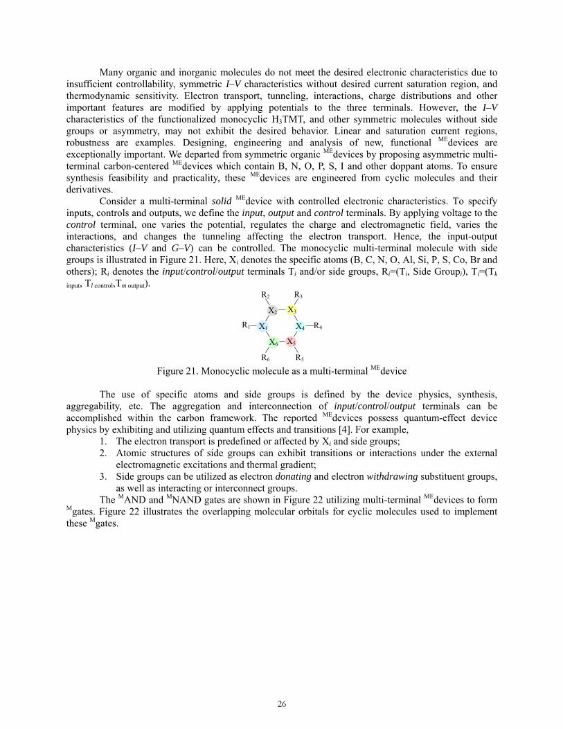
26
Many organic and inorganic molecules do not meet the desired electronic characteristics due to insufficient controllability, symmetric I–V characteristics without desired current saturation region, and thermodynamic sensitivity. Electron transport, tunneling, interactions, charge distributions and other important features are modified by applying potentials to the three terminals. However, the I–V characteristics of the functionalized monocyclic H3TMT, and other symmetric molecules without side groups or asymmetry, may not exhibit the desired behavior. Linear and saturation current regions, robustness are examples. Designing, engineering and analysis of new, functional MEdevices are exceptionally important. We departed from symmetric organic MEdevices by proposing asymmetric multi-terminal carbon-centered MEdevices which contain B, N, O, P, S, I and other doppant atoms. To ensure synthesis feasibility and practicality, these MEdevices are engineered from cyclic molecules and their derivatives. Consider a multi-terminal solid MEdevice with controlled electronic characteristics. To specify inputs, controls and outputs, we define the input, output and control terminals. By applying voltage to the control terminal, one varies the potential, regulates the charge and electromagnetic field, varies the interactions, and changes the tunneling affecting the electron transport. Hence, the input-output characteristics (I–V and G–V) can be controlled. The monocyclic multi-terminal molecule with side groups is illustrated in Figure 21. Here, Xi denotes the specific atoms (B, C, N, O, Al, Si, P, S, Co, Br and others); Ri denotes the input/control/output terminals Ti and/or side groups, Ri=(Ti, Side Groupi), Ti=(Tk
input, Tl control,Tm output).
X1
X3
X5
X2
X6
X4
R6
R2 R3
R1 R4
R5 Figure 21. Monocyclic molecule as a multi-terminal MEdevice
The use of specific atoms and side groups is defined by the device physics, synthesis, aggregability, etc. The aggregation and interconnection of input/control/output terminals can be accomplished within the carbon framework. The reported MEdevices possess quantum-effect device physics by exhibiting and utilizing quantum effects and transitions [4]. For example,
1. The electron transport is predefined or affected by Xi and side groups; 2. Atomic structures of side groups can exhibit transitions or interactions under the external
electromagnetic excitations and thermal gradient; 3. Side groups can be utilized as electron donating and electron withdrawing substituent groups,
as well as interacting or interconnect groups. The MAND and MNAND gates are shown in Figure 22 utilizing multi-terminal MEdevices to form Mgates. Figure 22 illustrates the overlapping molecular orbitals for cyclic molecules used to implement these Mgates.

27
Figure 22. MAND and MNAND gates comprised from cyclic molecules The Mgates, designed using cyclic molecules as MEdevices, are depicted in Figure 23.
Figure 23. Molecular gates: Minverter, MAND, MNAND, MOR, MNOR, MXOR and MMUX which can be utilized in the implementation of ℵhypercells We considered a three-terminal MEdevice with the input, control and output terminals as shown in Figures 21 and 24. The device physics of the proposed MEdevice is based on the quantum interaction and controlled electron transport. The applied Vcontrol(t) changes the charge distribution ρ(t,r) and EE(t,r) affecting the electron flow. This MEdevice operates in the controlled electron-exchangeable environment due to quantum effects. Controlled super-fast potential-assisted electron transport can be achieved [4]. Electron-exchangeable environmental interactions qualitatively and quantitatively modify the device behavior and its characteristics. Consider electron transport in the time- and spatial-varying metastable potentials Π(t,r). From the quantum theory viewpoint, the changes in the Hamiltonian result in changes of tunneling T(E) and quantum transitions due to variations of ρ(t,r), EE(t,r) and Π(t,r). The device

28
controllability is ensured by varying Vcontrol(t) that affects the device switching, I–V and other characteristics.
Vinput
Vcontrol
Voutput
Figure 24. Three-terminal MEdevice comprised from a cyclic molecule with a carbon interconnecting framework
We performed high-fidelity modeling and data-intensive analysis for the studied MEdevice. For heterojunction microelectronic devices, one usually solves the one-dimensional Schrödinger and Poisson equations applying the Fermi-Dirac distribution function. In contrast, for the devised MEdevices, a 3D problem arises which cannot be simplified. Furthermore, the distribution functions and statistical mechanics postulates may not be straightforwardly applied [4]. For the studied cyclic molecule which forms an interconnected MEdevice, we consider 9 atoms with motionless protons with charges qi.
The radial Coulomb potentials are r
qZr iieff
i0
2
4)(
πε−=Π . For carbon Zeff C=3.14.
Using the spherical coordinate system, the Schrödinger equation
),,(),,(),,(sin1sin
sin11
2 2
2
2222
2
2
φθφθφθφθθ
θθθ
rErrrrr
rrrm
Ψ=ΨΠ+⎥⎦
⎤⎢⎣
⎡∂
Ψ∂+⎟
⎠⎞
⎜⎝⎛
∂Ψ∂
∂∂
+⎟⎠⎞
⎜⎝⎛
∂Ψ∂
∂∂
−h
should be solved. It is impractical to find the analytic solution by using the separation of variables concept. Instead, the Schrödinger and Poisson equations were discretized in order to numerically solve these differential equations. The magnitude of the time-varying potential applied to the control terminal is bounded due to the thermal stability of the molecule, e.g., |Vcontrol| ≤ Vcontrol max. We let |Vcontrol| ≤ 0.2 V. The charge distribution is of particular interest. Figure 25 documents a three-dimensional charge distribution in the molecule if Vcontrol = 0.1 V and Vcontrol = 0.2 V. The total molecular charge distribution was found by summing the individual orbital densities.
Figure 25. Charge distribution ρ(r) The Schrödinger and Poisson equations were solved using a self-consistent algorithm in order to verify the soundness of the device physics and examine the baseline performance characteristics. To obtain the current density j and current in the MEdevice, the velocity and momentum of the electrons were
obtained by making use of rrr
r dtitp ),(),(* Ψ⎟⎠⎞
⎜⎝⎛
∂∂
−Ψ= ∫∞
∞−
h . The wave function Ψ(t,r) was derived for
distinct values of Vcontrol. The I–V characteristics of the studied MEdevice for two different control currents (0.1 and 0.2 nA) are given in Figure 26. The results documented imply that the proposed MEdevice may be
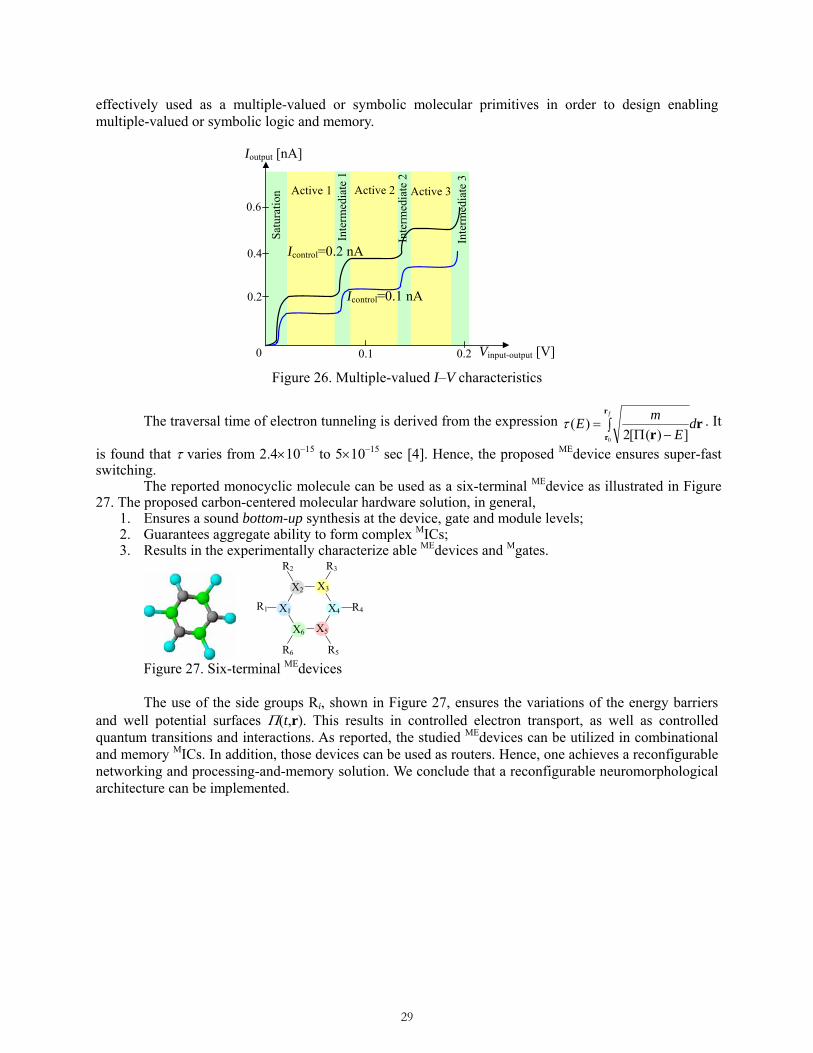
29
effectively used as a multiple-valued or symbolic molecular primitives in order to design enabling multiple-valued or symbolic logic and memory.
Vinput-output [V]
Satu
ratio
n Active 1 Active 2 Active 3
Inte
rmed
iate
1
Inte
rmed
iate
2
Inte
rmed
iate
3
0.20.1
Ioutput [nA]
0.2
0.4
0.6
Icontrol=0.1 nA
Icontrol=0.2 nA
0
Figure 26. Multiple-valued I–V characteristics
The traversal time of electron tunneling is derived from the expression ∫−Π
=f
dE
mEr
rr
r0 ])([2)(τ . It
is found that τ varies from 2.4×10⁻¹⁵ to 5×10–15 sec [4]. Hence, the proposed MEdevice ensures super-fast switching. The reported monocyclic molecule can be used as a six-terminal MEdevice as illustrated in Figure 27. The proposed carbon-centered molecular hardware solution, in general,
1. Ensures a sound bottom-up synthesis at the device, gate and module levels; 2. Guarantees aggregate ability to form complex MICs; 3. Results in the experimentally characterize able MEdevices and Mgates.
X1
X3
X5
X2
X6
X4
R6
R2 R3
R1 R4
R5 Figure 27. Six-terminal MEdevices
The use of the side groups Ri, shown in Figure 27, ensures the variations of the energy barriers and well potential surfaces Π(t,r). This results in controlled electron transport, as well as controlled quantum transitions and interactions. As reported, the studied MEdevices can be utilized in combinational and memory MICs. In addition, those devices can be used as routers. Hence, one achieves a reconfigurable networking and processing-and-memory solution. We conclude that a reconfigurable neuromorphological architecture can be implemented.
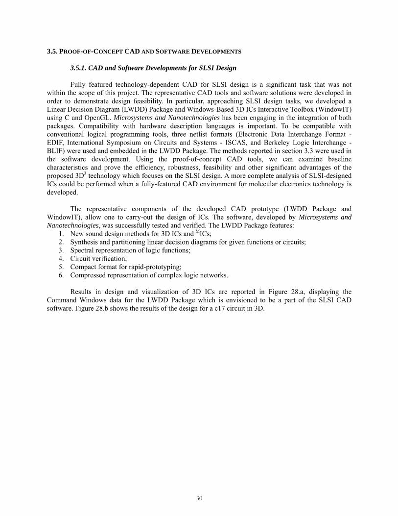
30
3.5. PROOF-OF-CONCEPT CAD AND SOFTWARE DEVELOPMENTS
3.5.1. CAD and Software Developments for SLSI Design Fully featured technology-dependent CAD for SLSI design is a significant task that was not
within the scope of this project. The representative CAD tools and software solutions were developed in order to demonstrate design feasibility. In particular, approaching SLSI design tasks, we developed a Linear Decision Diagram (LWDD) Package and Windows-Based 3D ICs Interactive Toolbox (WindowIT) using C and OpenGL. Microsystems and Nanotechnologies has been engaging in the integration of both packages. Compatibility with hardware description languages is important. To be compatible with conventional logical programming tools, three netlist formats (Electronic Data Interchange Format - EDIF, International Symposium on Circuits and Systems - ISCAS, and Berkeley Logic Interchange - BLIF) were used and embedded in the LWDD Package. The methods reported in section 3.3 were used in the software development. Using the proof-of-concept CAD tools, we can examine baseline characteristics and prove the efficiency, robustness, feasibility and other significant advantages of the proposed 3D3 technology which focuses on the SLSI design. A more complete analysis of SLSI-designed ICs could be performed when a fully-featured CAD environment for molecular electronics technology is developed.
The representative components of the developed CAD prototype (LWDD Package and
WindowIT), allow one to carry-out the design of ICs. The software, developed by Microsystems and Nanotechnologies, was successfully tested and verified. The LWDD Package features:
1. New sound design methods for 3D ICs and MICs; 2. Synthesis and partitioning linear decision diagrams for given functions or circuits; 3. Spectral representation of logic functions; 4. Circuit verification; 5. Compact format for rapid-prototyping; 6. Compressed representation of complex logic networks.
Results in design and visualization of 3D ICs are reported in Figure 28.a, displaying the
Command Windows data for the LWDD Package which is envisioned to be a part of the SLSI CAD software. Figure 28.b shows the results of the design for a c17 circuit in 3D.

31
(a)
(b)
Figure 28. (a) Command Window of the LWDD Package to perform design of ICs in 3D; (b) Design of c17 circuit, and c17 implementation using MNAND gates. The results of the design for an 8-bit ALU, e.g., well-known c880, are displayed in Figure 29.
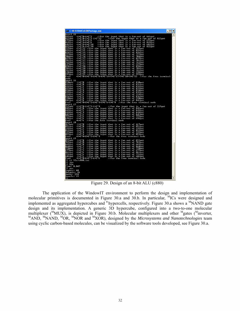
32
Figure 29. Design of an 8-bit ALU (c880)
The application of the WindowIT environment to perform the design and implementation of molecular primitives is documented in Figure 30.a and 30.b. In particular, MICs were designed and implemented as aggregated hypercubes and ℵhypercells, respectively. Figure 30.a shows a MNAND gate design and its implementation. A generic 3D hypercube, configured into a two-to-one molecular multiplexer (MMUX), is depicted in Figure 30.b. Molecular multiplexers and other Mgates (Minverter, MAND, MNAND, MOR, MNOR and MXOR), designed by the Microsystems and Nanotechnologies team using cyclic carbon-based molecules, can be visualized by the software tools developed, see Figure 30.a.
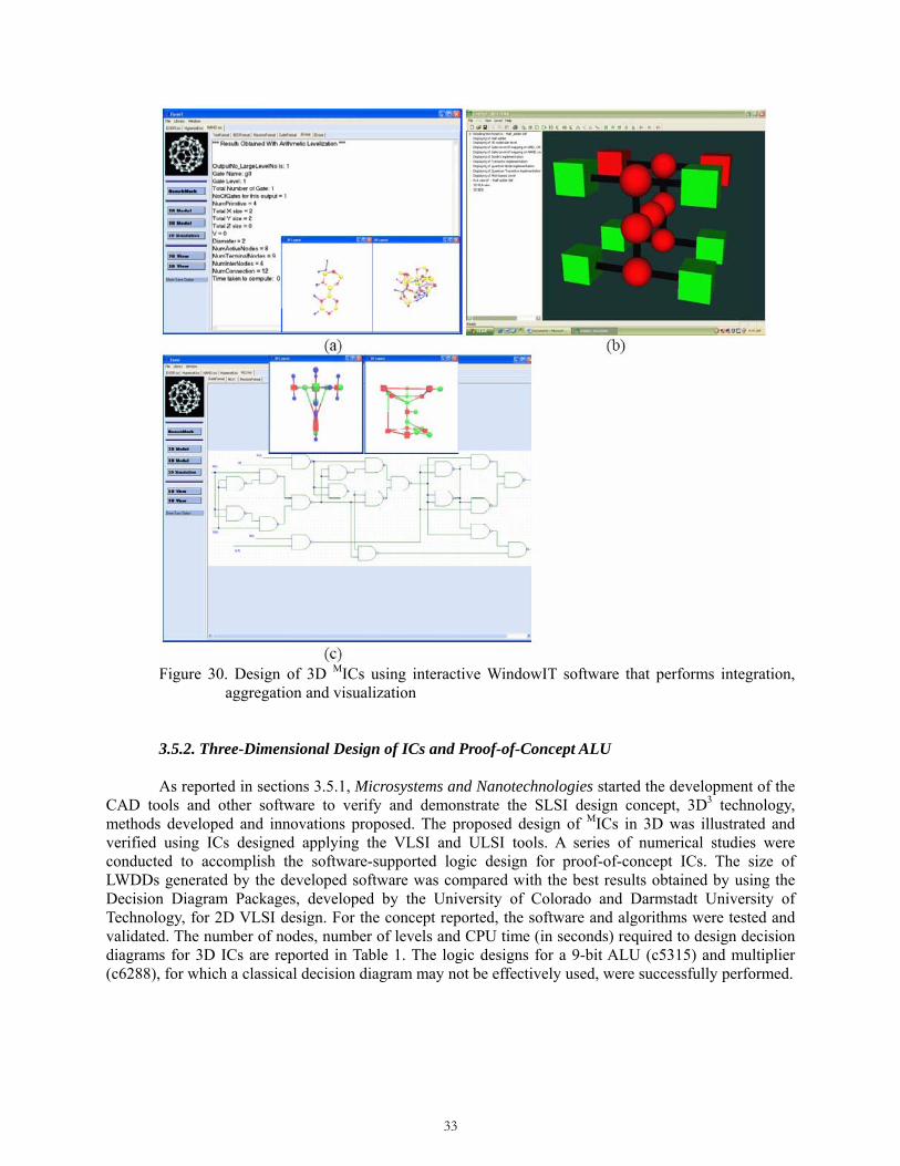
33
Figure 30. Design of 3D MICs using interactive WindowIT software that performs integration,
aggregation and visualization
3.5.2. Three-Dimensional Design of ICs and Proof-of-Concept ALU As reported in sections 3.5.1, Microsystems and Nanotechnologies started the development of the CAD tools and other software to verify and demonstrate the SLSI design concept, 3D3 technology, methods developed and innovations proposed. The proposed design of MICs in 3D was illustrated and verified using ICs designed applying the VLSI and ULSI tools. A series of numerical studies were conducted to accomplish the software-supported logic design for proof-of-concept ICs. The size of LWDDs generated by the developed software was compared with the best results obtained by using the Decision Diagram Packages, developed by the University of Colorado and Darmstadt University of Technology, for 2D VLSI design. For the concept reported, the software and algorithms were tested and validated. The number of nodes, number of levels and CPU time (in seconds) required to design decision diagrams for 3D ICs are reported in Table 1. The logic designs for a 9-bit ALU (c5315) and multiplier (c6288), for which a classical decision diagram may not be effectively used, were successfully performed.

34
Table 1. Design summary (number of nodes, levels and CPU time) for BDD, WDD and LWDD Circuit I/O BDD WDD
#N LWDD (EDIF)
#L #N CPU Time LWDD (ISCAS’85) #L #N CPU Time
C432 36/7 1064 1209 21 455 <0.01 17 336 <0.001 8-bit ALU C880 60/26
4053 4048 35 604 <0.01 24 605 <0.1
c2670 233/140 1850 3939 40 1374 <0.1 32 2026 <0.1 9-bit ALU c5315 178/123
1719 2504
68 3192 <0.3
49 4156 <0.4
Multiplier c6288 32/32
– –
124 4320 <0.2
124 4318 <0.5
In the design we assumed: (1) Feedforward neural network without feedback; (2) Threshold Mgates were used; (3) Aggregated networked 3D ℵhypercells were comprised from Mgates; (4) Multilevel combinational circuits were used over the library of NAND, NOR and EXOR Mgates. Numerical studies (design) were conducted for different circuits. The results are reported in Tables 1 and 2 for the representative circuits (for which the conventional methods result in some inconsistencies or drawbacks). We examine volumistic size, topological parameters, performance and validate the design. The space size is given by X, Y and Z that result in the volumistic (V) quantity V=X×Y×Z. The topological characteristics were evaluated using the total number of terminals (NT) and intermediate (NI) nodes. A 3D 9-bit ALU (c5315) with 178 inputs and 123 outputs was implemented using 1413 Mgates, while a c6288 multiplier (32 inputs and 32 outputs) has 2327 Mgates. The number of incompletely specified hypercubes and ℵhypercells was minimized. The hypercubes in the ith layer were connected to the corresponding cubes in the (i–1)th and (i+1)th layers. The obtained 3D topology had X×Y×Z hypercubes. The number of terminal nodes and intermediate nodes were 3750 and 2813 for a 9-bit ALU, while, for a multiplier, we had 9248 and 6916 nodes. To combine all layers, more than 10,000 connections were generated. The design in 3D was performed within 0.4 seconds. Other metrics to evaluate the designed 3D ICs were used. In addition to conventional parameters (diameter, dilation cost, expansion, load, etc.), we used the number of variables in the logic function described by hypercubes, number of links, fan-out of the intermediate nodes, statistics, etc. Table 2. Numerical results for 3D ICs
Circuit I/O Space Size #G #X #Y #Z
Nodes and Connections #NT # NI CPU Time
c432 36/7 126 66 64 66 2022 1896 <0.01 8-bit ALU c880 60/26
294 70 72 70
612 482 <0.1
c2670 233/140 828 82 80 78 3594 2766 <0.1 9-bit ALU c5315 178/123
1413 138 132 126
3750 2813 <0.4
Multiplier c6288 32/32
2327 248 248 244
9246 6916 <0.5
Comparison of 2D and 3D designs for a 9-bit ALU. The high-level ALU model is documented in Figure 31. The studied ALU performs arithmetic and logic operations simultaneously on two 9-bit input data words, and computes the parity of the results. Conventional 2D logic design of a 9-bit ALU (c5315 circuit) with 178 inputs and 123 outputs results in 2406 gates. In contrast, the proposed design, carried-
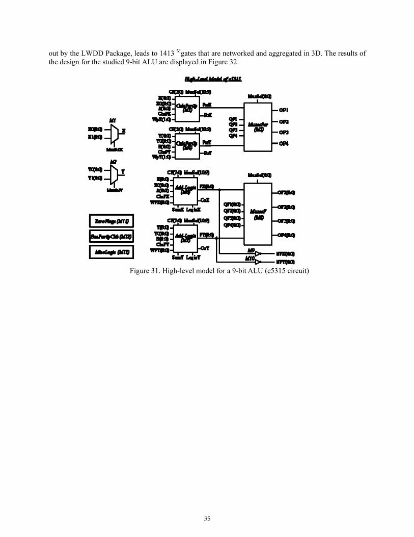
35
out by the LWDD Package, leads to 1413 Mgates that are networked and aggregated in 3D. The results of the design for the studied 9-bit ALU are displayed in Figure 32.
Figure 31. High-level model for a 9-bit ALU (c5315 circuit)

36
Figure 32. Design of a 9-bit ALU

37
4. CONCLUSIONS As documented in this report, Microsystems and Nanotechnologies has successfully completed all Tasks outlined in the Statement of Work. Innovative developments in devising, design and analysis of novel molecular computing and processing platforms were carried-out and reported. Enabling hardware and software solutions were proposed, which ultimately resulted in the development of 3D3 technology. Molecular electronics and MICs, were examined. These innovations are leading to super-high-performance computing uniquely utilizing proposed 3D-topology MEdevices, ℵhypercells, fused processing-and-memory organization, reconfigurable 3Dnetworking-and-processing neuromorphological architecture and SLSI design. A wide spectrum of fundamental, applied and experimental issues, related to the design, device physics, functionality, performance and capabilities were studied and are under further development. An innovative concept in SLSI design of MICs was reported. This concept was verified and demonstrated for various circuits demonstrating the applicability the design method reported and the effectiveness of representative CAD tools. Though a great number of problems remain to be addressed and solved, it was demonstrated that the proposed molecular computing platforms provide overall supremacy ensuring high-performance processing. We focused on development of a feasible, practical, affordable and superior 3D3 technology for massive parallel distributed computing and processing for Air Force systems.

38
REFERENCES
1. International Technology Roadmap for Semiconductors, 2005 Edition, Semiconductor Industry Association (SIA), SEMATECH, Austin, Texas, USA, 2005.
2. J. C. Ellenbogen and J. C. Love, “Architectures for molecular electronic computers: Logic structures and an adder designed from molecular electronic diodes,” Proc. IEEE, vol. 88, no. 3, pp. 386-426, 2000.
3. J. R. Heath and M. A. Ratner, “Molecular electronics,” Physics Today, no. 1, pp. 43-49, 2003. 4. S. E. Lyshevski, Molecular Electronics, Circuits and Processing Platforms, CRC Press, Boca Raton,
FL, 2007. 5. S. E. Lyshevski, NEMS and MEMS: Fundamentals of Nano- and Microengineering, CRC Press,
Boca Raton, FL, 2005. 6. S. E. Lyshevski, Three-Dimensional Molecular Electronics and Integrated Circuits For Signal
and Information Processing Platforms, Handbook on Nano and Molecular Electronics, Ed. S. E. Lyshevski, CRC Press, Boca Raton, FL, pp. 6-1 - 6-104, 2007.
7. S. E. Lyshevski, Molecular Computing and Processing Platforms, Handbook of Nanoscience, Engineering and Technology, Ed. W. Goddard, D. Brenner, S. E. Lyshevski and G. Iafrate, CRC Press, Boca Raton, FL, 2007.
8. W. Porod, Nanoelectronic Circuit Architectures, Handbook of Nanoscience, Engineering and Technology, Eds. W. A. Goddard, D. W. Brenner, S. E. Lyshevski and G. J. Iafrate, pp. 5.1– 5.12, 2003.
9. S. R. Williams and P. J. Kuekes, “Molecular nanoelectronics,” Proc. Int. Symposium on Circuits and Systems, Geneva, Switzerland, vol. 1, pp. 5 – 7, 2000.
10. V. D. Malyugin, “Realization of corteges of Boolean functions by linear arithmetical polynomials,” Automica and Telemekhica, no. 2, pp. 114-121, 1984.
11. S. Yanushkevich, V. Shmerko and S. E. Lyshevski, Logic Design of NanoICs, CRC Press, Boca Raton, FL, 2005.
12. A. Carbone and N. C. Seeman, “Circuits and programmable self-assembling DNA structures,” Proc. Nat. Acad. Science, vol. 99, no. 20, pp. 12577-12582, 2002.
13. N. C. Seeman, “DNA engineering and its application to nanotechnology,” Nanotechnology, vol. 17, pp. 437-443, 1999.
14. J. Chen, T. Lee, J. Su, W. Wang, M. A. Reed, A. M. Rawlett, M. Kozaki, Y. Yao, R. C. Jagessar, S. M. Dirk, D. W. Price, J. M. Tour, D. S. Grubisha and D. W. Bennett, Molecular Electronic Devices, Handbook Molecular Nanoelectronics, Eds. M. A. Reed and L. Lee, American Science Publishers, 2003.
15. K. Lee, J. Choi and D. B. Janes, “Measurement of I-V characteristic of organic molecules using step junction,” Proc. IEEE Conference on Nanotechnology, Munich, Germany, pp. 125-127, 2004.
16. A. K. Mahapatro, S. Ghosh and D. B. Janes, “Nanometer scale electrode separation (nanogap) using electromigration at room temperature,” Proc. IEEE Trans. Nanotechnology, vol. 5, no. 3, pp. 232-236, 2006.
17. R. M. Metzger, Unimolecular Electronics: Results and Prospects, Handbook on Molecular and NanoElectronics, Ed. S. E. Lyshevski, CRC Press, Boca Raton, FL, 2007.
18. J. Reichert, R. Ochs, D. Beckmann, H. B. Weber, M. Mayor and H. V. Lohneysen, “Driving current through single organic molecules,” Physical Review Letters, vol. 88, no. 17, 2002.
19. J. M. Tour and D. K. James, Molecular Electronic Computing Architectures, Handbook of Nanoscience, Engineering and Technology, Eds. W. A. Goddard, D. W. Brenner, S. E. Lyshevski and G. J. Iafrate, pp. 4.1–4.28, 2003.

39
20. W. Wang, T. Lee, I. Kretzschmar and M. A. Reed, “Inelastic electron tunneling spectroscopy of an alkanedithiol self-assembled monolayer,” Nano Letters, vol. 4, no. 4, pp. 643-646, 2004.
21. A. K. Mahapatro, D. B. Janes, K. J. Jeong and G. U. Lee, “Electrical Behavior of Nano-scale Junctions with Well Engineered Double Stranded DNA Molecules,” Proc. IEEE Conference on Nanotechnology, Cincinnati, OH, 2006.
22. D. Porath, “Direct measurement of electrical transport through DNA molecules,” Nature, vol. 403, pp. 635-638, 2000.
23. D. Porath, G. Cuniberti and R. Di Felice, “Charge transport in DNA-based devices,” Top. Curr. Chem., vol. 237, pp. 183-227, 2004.
24. A. Rakitin, P. Aich, C. Papadopoulos, Y. Kobzar, A. S. Vedeneev, J. S. Lee and J. M. Xu, “Metallic conduction through engineered DNA: DNA nanoelectronic building blocks,” Physical Review Letters, vol. 86, no. 16, pp. 3670-3673, 2001.
25. M. A. Lyshevski, "Multi-valued DNA-based electronic nanodevices," IEEE Conf. Multi-Valued Logic Design, Calgary, Canada, 2005.
26. R. Rinaldi, E. Branca, R. Cingolani, S. Masiero, G. P. Spada and G. Gottarelli, “Photodetectors fabricated from a self-assembly of a deoxyguanosine derivative,” Applied Physics Letters, vol. 78, no. 22, pp. 3541-3543, 2001.
27. K. H. Yoo, D. H. Ha, J. O. Lee, J. W. Park, J. Kim, J. J. Kim, H. Y. Lee, T. Kawai and H. Y. Choi, “Electrical conduction through poly(dA)-poly(dT) and poly(dG)-poly(dC) DNA molecules,” Physical Review Letters, vol. 87, no. 19, 2001
28. S. M. Sze and K. K. Ng, Physics of Semiconductor Devices, John Wiley and Sons, NJ, 2007. 29. A. Aviram and M. A. Ratner, “Molecular rectifiers,” Chem. Phys. Letters, vol. 29, pp. 277-283,
1974.
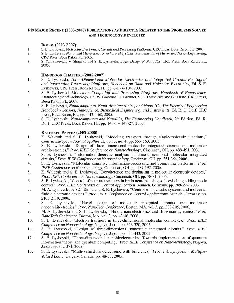
40
PIS MAJOR RECENT (2005-2006) PUBLICATIONS AS DIRECTLY RELATED TO THE PROBLEMS SOLVED AND TECHNOLOGY DEVELOPED
BOOKS (2005-2007): 1. S. E. Lyshevski, Molecular Electronics, Circuits and Processing Platforms, CRC Press, Boca Raton, FL, 2007. 2. S. E. Lyshevski, Nano- and Micro-Electromechanical Systems: Fundamental of Micro- and Nano- Engineering,
CRC Press, Boca Raton, FL, 2005. 3. S. Yanushkevich, V. Shmerko and S. E. Lyshevski, Logic Design of Nano-ICs, CRC Press, Boca Raton, FL,
2005.
HANDBOOK CHAPTERS (2005-2007): 1. S. E. Lyshevski, Three-Dimensional Molecular Electronics and Integrated Circuits For Signal
and Information Processing Platforms, Handbook on Nano and Molecular Electronics, Ed. S. E. Lyshevski, CRC Press, Boca Raton, FL, pp. 6-1 - 6-104, 2007.
2. S. E. Lyshevski, Molecular Computing and Processing Platforms, Handbook of Nanoscience, Engineering and Technology, Ed. W. Goddard, D. Brenner, S. E. Lyshevski and G. Iafrate, CRC Press, Boca Raton, FL, 2007.
3. S. E. Lyshevski, Nanocomputers, Nano-Architectronics, and Nano-ICs, The Electrical Engineering Handbook - Sensors, Nanoscience, Biomedical Engineering, and Instruments, Ed. R. C. Dorf, CRC Press, Boca Raton, FL, pp. 4-42-4-68, 2005.
4. S. E. Lyshevski, Nanocomputers and NanoICs, The Engineering Handbook, 2nd Edition, Ed. R. Dorf, CRC Press, Boca Raton, FL, pp. 148-1 – 148-27, 2005.
REFEREED PAPERS (2005-2006):
1. K. Walczak and S. E. Lyshevski, ”Modeling transport through single-molecule junctions,” Central European Journal of Physics, vol. 3, no. 4, pp. 555-563, 2005.
2. S. E. Lyshevski, “Design of three-dimensional molecular integrated circuits and molecular architectronics,” Proc. IEEE Conference on Nanotechnology, Cincinnati, OH, pp. 488-491, 2006.
3. S. E. Lyshevski, “Information-theoretic analysis of three-dimensional molecular integrated circuits,” Proc. IEEE Conference on Nanotechnology, Cincinnati, OH, pp. 351-354, 2006.
4. S. E. Lyshevski, “Molecular cognitive information-processing and computing platforms,” Proc. IEEE Conference on Nanotechnology, Cincinnati, OH, pp. 189-192, 2006.
5. K. Walczak and S. E. Lyshevski, “Decoherence and dephasing in molecular electronic devices,” Proc. IEEE Conference on Nanotechnology, Cincinnati, OH, pp. 78-81, 2006.
6. S. E. Lyshevski, “Control of neurotransmitters in brain neurons using soft-switching sliding mode control,” Proc. IEEE Conference on Control Applications, Munich, Germany, pp. 289-294, 2006.
7. M. A. Lyshevski, A.S.C. Sinha and S. E. Lyshevski, “Control of stochastic systems and molecular fluidic electronic devices,” Proc. IEEE Conference on Control Applications, Munich, Germany, pp. 2105-2110, 2006.
8. S. E. Lyshevski, “Novel design of molecular integrated circuits and molecular nanoarchitectronics,” Proc. NanoTech Conference, Boston, MA, vol. 3, pp. 202-205, 2006.
9. M. A. Lyshevski and S. E. Lyshevski, “Fluidic nanoelectronics and Brownian dynamics,” Proc. NanoTech Conference, Boston, MA, vol. 3, pp. 43-46, 2006.
10. S. E. Lyshevski, “Electron transport in three-dimensional molecular complexes,” Proc. IEEE Conference on Nanotechnology, Nagoya, Japan, pp. 318-320, 2005.
11. S. E. Lyshevski, “Design of three-dimensional nanoscale integrated circuits,” Proc. IEEE Conference on Nanotechnology, Nagoya, Japan, pp. 441-443, 2005.
12. S. E. Lyshevski, “Three-dimensional nanobioelectronics: Towards implementation of quantum information theory and quantum computing,” Proc. IEEE Conference on Nanotechnology, Nagoya, Japan, pp. 372-374, 2005.
13. S. E. Lyshevski, “Multi-valued nanoelectronic with fullerenes,” Proc. Int. Symposium Multiple-Valued Logic, Calgary, Canada, pp. 48-53, 2005.
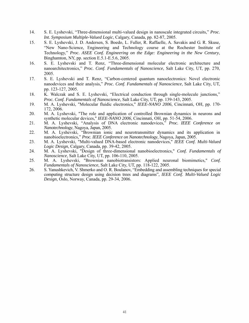
41
14. S. E. Lyshevski, “Three-dimensional multi-valued design in nanoscale integrated circuits,” Proc. Int. Symposium Multiple-Valued Logic, Calgary, Canada, pp. 82-87, 2005.
15. S. E. Lyshevski, J. D. Andersen, S. Boedo, L. Fuller, R. Raffaelle, A. Savakis and G. R. Skuse, “New Nano-Science, Engineering and Technology course at the Rochester Institute of Technology,” Proc. ASEE Conf. Engineering on the Edge: Engineering in the New Century, Binghamton, NY, pp. section E.5.1-E.5.6, 2005.
16. S. E. Lyshevski and T. Renz, “Three-dimensional molecular electronic architecture and nanoarchitectronics,” Proc. Conf. Fundamentals of Nanoscience, Salt Lake City, UT, pp. 270, 2005.
17. S. E. Lyshevski and T. Renz, “Carbon-centered quantum nanoelectronics: Novel electronic nanodevices and their analysis,” Proc. Conf. Fundamentals of Nanoscience, Salt Lake City, UT, pp. 123-127, 2005.
18. K. Walczak and S. E. Lyshevski, “Electrical conduction through single-molecule junctions,” Proc. Conf. Fundamentals of Nanoscience, Salt Lake City, UT, pp. 139-143, 2005.
19. M. A. Lyshevski, "Molecular fluidic electronics," IEEE-NANO 2006, Cincinnati, OH, pp. 170-172, 2006.
20. M. A. Lyshevski, "The role and application of controlled Brownian dynamics in neurons and synthetic molecular devices," IEEE-NANO 2006, Cincinnati, OH, pp. 51-54, 2006.
21. M. A. Lyshevski, “Analysis of DNA electronic nanodevices,” Proc. IEEE Conference on Nanotechnology, Nagoya, Japan, 2005.
22. M. A. Lyshevski, “Brownian ionic and neurotransmitter dynamics and its application in nanobioelectronics,” Proc. IEEE Conference on Nanotechnology, Nagoya, Japan, 2005.
23. M. A. Lyshevski, "Multi-valued DNA-based electronic nanodevices," IEEE Conf. Multi-Valued Logic Design, Calgary, Canada, pp. 39-42, 2005.
24. M. A. Lyshevski, "Design of three-dimensional nanobioelectronics," Conf. Fundamentals of Nanoscience, Salt Lake City, UT, pp. 106-110, 2005.
25. M. A. Lyshevski, "Brownian nanobiotransistors: Applied neuronal biomimetics," Conf. Fundamentals of Nanoscience, Salt Lake City, UT, pp. 118-122, 2005.
26. S. Yanushkevich, V. Shmerko and O. R. Boulanov, “Embedding and assembling techniques for special computing structure design using decision trees and diagrams”, IEEE Conf. Multi-Valued Logic Design, Oslo, Norway, Canada, pp. 29-34, 2006.

42
LIST OF ABBREVIATIONS AND ACRONYMS
2D - Two-dimensional 3D - Three-dimensional ALU - Arithmetic logic unit BJT - Bipolar junction transistor CAD - Computer-aided-design CMOS - Complimentary metal-oxide semiconductor DD - Decision diagram DNA -Deoxyribonucleic acid dsDNA - Double stranded DNA FET - Field-effect transistor G–V - Conductance-voltage characteristic HOMO - Highest occupied molecular orbital ℵhypercell - Neuronal hypercell IC - Integrated circuit MIC - Molecular integrated circuit
MEdevice - Molecular Electronics device I–V - Current-voltage characteristic Mgate - Molecular gate MMUX - Molecular Multiplexers LWDD - Linear decision diagrams LP - Linear arithmetic polynomial LUMO - Lowest unoccupied molecular orbital LWDD - Linear word-level decision diagrams

43
SLSI - Super-large-scale integration SOW - Statement of Work SRAM - Static random access memory VLSI - Very-large-scale integration ULSI - Ultra-large-scale integration