This document is downloaded from the Digital Open Access ... · PDF fileof ALD has been...
13
This document is downloaded from the Digital Open Access Repository of VTT VTT http://www.vtt.fi P.O. box 1000 FI-02044 VTT Finland By using VTT Digital Open Access Repository you are bound by the following Terms & Conditions. I have read and I understand the following statement: This document is protected by copyright and other intellectual property rights, and duplication or sale of all or part of any of this document is not permitted, except duplication for research use or educational purposes in electronic or print form. You must obtain permission for any other use. Electronic or print copies may not be offered for sale. Title Microscratch testing method for systematic evaluation of the adhesion of atomic layer deposited thin films on silicon Author(s) Kilpi, Lauri; Ylivaara, Oili M.E.; Vaajoki, Antti; Malm, Jari; Sintonen, Sakari; Tuominen, Marko; Puurunen, Riikka L.; Ronkainen, Helena Citation Journal of Vacuum Science and Technology A: Vacuum, Surfaces and Films. AIP Publishing. Vol. 34 (2016) No: 1, 01A124 Date 2016 URL http://dx.doi.org/10.1116/1.4935959 Rights This arcticle may be downloaded for personal use only.
Transcript of This document is downloaded from the Digital Open Access ... · PDF fileof ALD has been...

This document is downloaded from the Digital Open Access Repository of VTT
VTT
http://www.vtt.fi P.O. box 1000 FI-02044 VTT Finland
By using VTT Digital Open Access Repository you are bound by the following Terms & Conditions.
I have read and I understand the following statement:
This document is protected by copyright and other intellectual property rights, and duplication or sale of all or part of any of this document is not permitted, except duplication for research use or educational purposes in electronic or print form. You must obtain permission for any other use. Electronic or print copies may not be offered for sale.
Title Microscratch testing method for systematic
evaluation of the adhesion of atomic layer
deposited thin films on silicon
Author(s) Kilpi, Lauri; Ylivaara, Oili M.E.; Vaajoki, Antti;
Malm, Jari; Sintonen, Sakari; Tuominen, Marko;
Puurunen, Riikka L.; Ronkainen, Helena
Citation Journal of Vacuum Science and Technology A:
Vacuum, Surfaces and Films. AIP Publishing.
Vol. 34 (2016) No: 1, 01A124
Date 2016
URL http://dx.doi.org/10.1116/1.4935959
Rights This arcticle may be downloaded for personal
use only.
Microscratch testing method for systematic evaluation of the adhesion of atomic layerdeposited thin films on siliconLauri Kilpi, Oili M. E. Ylivaara, Antti Vaajoki, Jari Malm, Sakari Sintonen, Marko Tuominen, Riikka L. Puurunen,and Helena Ronkainen Citation: Journal of Vacuum Science & Technology A 34, 01A124 (2016); doi: 10.1116/1.4935959 View online: http://dx.doi.org/10.1116/1.4935959 View Table of Contents: http://scitation.aip.org/content/avs/journal/jvsta/34/1?ver=pdfcov Published by the AVS: Science & Technology of Materials, Interfaces, and Processing Articles you may be interested in Adhesion testing of atomic layer deposited TiO2 on glass substrate by the use of embedded SiO2 microspheres J. Vac. Sci. Technol. A 32, 01A102 (2014); 10.1116/1.4827197 Atomic layer deposition onto carbon fiber: From single layer deposition via multilayer structure to metal oxidemicrotubes J. Vac. Sci. Technol. A 31, 01A139 (2013); 10.1116/1.4768917 Optical properties of cobalt slanted columnar thin films passivated by atomic layer deposition Appl. Phys. Lett. 100, 011912 (2012); 10.1063/1.3675549 Electrical characteristics of Ga 2 O 3 – TiO 2 nanomixed films grown by plasma-enhanced atomic-layerdeposition for gate dielectric applications Appl. Phys. Lett. 87, 082909 (2005); 10.1063/1.2034100 High dielectric constant TiO 2 thin films on a Ru electrode grown at 250 °C by atomic-layer deposition Appl. Phys. Lett. 85, 4112 (2004); 10.1063/1.1812832
Redistribution subject to AVS license or copyright; see http://scitation.aip.org/termsconditions. IP: 130.188.24.113 On: Thu, 03 Mar 2016 08:43:00

Microscratch testing method for systematic evaluation of the adhesionof atomic layer deposited thin films on silicon
Lauri Kilpi,a) Oili M. E. Ylivaara, and Antti VaajokiVTT Technical Research Centre of Finland Ltd., P.O. Box 1000, FI-02044 VTT, Finland
Jari MalmDepartment of Physics, University of Jyv€askyl€a, P.O. Box 35, Jyv€askyl€a 40014, Finland
Sakari SintonenDepartment of Micro- and Nanosciences, Aalto University School of Electrical Engineering, P.O. Box 13500,FI-00076 AALTO, Finland
Marko TuominenASM Microchemistry Oy, Pietari Kalmin katu 1 F 2, FIN-00560 Helsinki, Finland
Riikka L. Puurunen and Helena RonkainenVTT Technical Research Centre of Finland Ltd., P.O. Box 1000, FI-02044 VTT, Finland
(Received 1 September 2015; accepted 2 November 2015; published 20 November 2015)
The scratch test method is widely used for adhesion evaluation of thin films and coatings. Usual
critical load criteria designed for scratch testing of coatings were not applicable to thin atomic
layer deposition (ALD) films on silicon wafers. Thus, the bases for critical load evaluation were
established and the critical loads suitable for ALD coating adhesion evaluation on silicon wafers
were determined in this paper as LCSi1, LCSi2, LCALD1, and LCALD2, representing the failure points
of the silicon substrate and the coating delamination points of the ALD coating. The adhesion
performance of the ALD Al2O3, TiO2, TiN, and TaCNþRu coatings with a thickness range
between 20 and 600 nm and deposition temperature between 30 and 410 �C on silicon wafers was
investigated. In addition, the impact of the annealing process after deposition on adhesion was
evaluated for selected cases. The tests carried out using scratch and Scotch tape test showed that
the coating deposition and annealing temperature, thickness of the coating, and surface
pretreatments of the Si wafer had an impact on the adhesion performance of the ALD coatings on
the silicon wafer. There was also an improved load carrying capacity due to Al2O3, the magnitude
of which depended on the coating thickness and the deposition temperature. The tape tests were
carried out for selected coatings as a comparison. The results show that the scratch test is a useful
and applicable tool for adhesion evaluation of ALD coatings, even when carried out for thin (20 nm
thick) coatings. VC 2015 American Vacuum Society. [http://dx.doi.org/10.1116/1.4935959]
I. INTRODUCTION
Atomic layer deposition (ALD) is a chemical vapor depo-
sition (CVD) method that allows deposition of uniform coat-
ings on complicated 3D geometries. The ALD technique is
based on sequential gas–solid reactions that are self-
terminating. ALD operates by exposing a solid surface alter-
nately to reactive gaseous chemicals, the exposures being
separated by purge/evacuation.1–3
One of the main motivations for the recent development
of ALD has been semiconductor processing. Miniaturization
in the semiconductor industry has led to the requirement for
atomic level control of thin film deposition.3 The films
deposited by ALD can also be utilized in microelectrome-
chanical systems (MEMS).4,5 The major benefit of ALD for
MEMS is the combination of low deposition temperatures
(often below 300 �C) with conformal coatings—the combi-
nation not achieved by conventional fabrication technolo-
gies.5,6 From the early 2000s, the reports of ALD for MEMS
deal with ALD as a tribological coating7 and an insulator
layer.8 Since then, ALD films have been demonstrated,
e.g., as dielectric layers in RF-MEMS,9 lubricating films,10
insulator in MEMS compass,11,12 mirrors in Fabry–Perot
interferometers for visible light,13,14 antistiction layers,15
and nanoelectromechanical system switches.16
The performance and reliability of MEMS devices can be
dominated by interfacial phenomena such as adhesion, friction,
and wear.7 Adhesion failure is often the primary failure mecha-
nism of the coating, limiting its applicability and lifetime.
Therefore, the adhesion to the substrate is one of the most
important functional requirements for the coatings.17 The adhe-
sion of ALD films is most often evaluated using Scotch tape
testing where a tape is pressed onto the film and rapidly
stripped.18 This method is highly qualitative, dependent on
user behavior. The method mainly distinguishes whether the
tested coating has poor adhesion properties or not. For these
reasons, a more controlled and quantitative method is needed.
Scratch testing is a widely used alternative to get quantitative
information about the adhesion behavior of the coatings19 and
has been recently utilized for ALD coatings.20–23
In a typical scratch testing setup, a diamond stylus is
drawn against the coating–substrate system with ana)Electronic mail: [email protected]
01A124-1 J. Vac. Sci. Technol. A 34(1), Jan/Feb 2016 0734-2101/2016/34(1)/01A124/11/$30.00 VC 2015 American Vacuum Society 01A124-1
Redistribution subject to AVS license or copyright; see http://scitation.aip.org/termsconditions. IP: 130.188.24.113 On: Thu, 03 Mar 2016 08:43:00
increasing load until the coating is removed from the sub-
strate or some other failure occurs. The load generating the
failure is determined as the critical load. The failure type in
scratch testing depends on several factors, such as the test
load, coating thickness, residual stress in the coating, proper-
ties of the substrate and coating, indenter radius, loading
rate, and sliding speed.24 For thin and hard coatings, the in-
denter tip has to be sufficiently large to induce an adequate
stress field to cause an adhesion failure. If the tip is too
sharp, the induced stress field might be bending, which, if
high enough, leads to cohesive failure of the coating.25 In
the scratch testing of hard coatings, there are two adhesion
related failure modes: wedge spallation and buckling.26
Buckling occurs for thin coatings which are able to bend in
response to applied stress whereas wedge spallation happens
usually for thicker (over 10 lm) coatings.26 Comparisons
between different samples using scratch testing are only
valid if the failure mechanism is the same in all samples.24
In this study, critical load criteria developed for ALD
films were used to describe the effect of deposition tempera-
ture, film thickness, and annealing temperature on the adhe-
sion performance of aluminum oxide (Al2O3), titanium
oxide (TiO2), titanium nitride (TiN), and tantalum carboni-
tride þ ruthenium (TaCNþRu) coatings. Also, the influence
of cleaning procedures on coating adhesion was evaluated.
For comparison, Scotch tape tests were carried out.
II. EXPERIMENT
A. ALD coating preparation
Single and double sided polished 150 mm p-type h100i sili-
con wafers with thicknesses of 380 and 675 lm were used as
substrates. Wafers were cleaned before the ALD using stand-
ard Radio Corporation of America (RCA) cleaning baths
(SC1, HF, and SC2),27 as described in previous work.21 For
selected wafers, the influence of substrate pretreatment to ad-
hesion was studied by cleaning wafers with SC1þHF
[H2O:HF (50%) 50:1] prior to ALD.
Aluminum oxide (Al2O3) and titanium dioxide (TiO2)
were grown in a top-flow PicosunTM R-150 ALD reactor.
Precursors were trimethylaluminum (Me3Al), titanium tetra-
chloride (TiCl4) and water (H2O). The intermediate space
pressure was about 7 hPa, and nitrogen (purity> 99.999%)
was used both as a purge gas and for flushing the reactant
lines with a constant 200 sccm flow. Electronic grade Me3Al
and TiCl4 precursors were from SAFC Hitech. Me3Al and
TiCl4 precursors were cooled with a Peltier element to about
17 and 14 �C, respectively. Water was used at room tempera-
ture without cooling. Precursor dose and purge times were 0.1
and 4.0 s, respectively, for Me3Al, TiCl4, and H2O. Samples
were grown at a temperature range from 110 to 300 �C using
0.1–4.0, 0.1–4.0, and 0.1–4.0 s for Me3Al, TiCl4, and H2O
pulse-purge sequences, respectively. For Al2O3 grown at
300 �C pulse sequence for Me3Al and H2O, pulse-purge was
0.1–1.0 and 0.1–1.0 s. The layer thicknesses were varied from
20 to 600 nm for Al2O3 and from 25 to 300 nm for TiO2.
ALD Al2O3 films for low temperature experiments were
deposited in a Beneq TFS 200 ALD reactor at 1.5 mbar
pressure and in the temperature range of 30–110 �C.
Precursors (Me3Al and H2O) were evaporated by means of
their own vapor pressure from external precursor bottles
kept at 20 �C. Electronic grade Me3Al precursor was from
SAFC Hitech. Nitrogen was used as the purge gas and it was
generated from compressed particle-free dry air by an
Inmatec PN-1150 molecular sieve nitrogen separator
(purity> 99.999%). The precursor pulses were kept at 0.15 s
and the purge periods following the Me3Al/H2O precursor
pulses were varied with deposition temperature, being 10/30,
7/20, 5/10, 4/5, and 2/3 s for samples deposited at 30, 50, 70,
90, and 110 �C, respectively. Hence, for example, the pulse
sequence for the sample deposited at 110 �C was 0.15–2.0
and 0.15–3.0 s. The number of deposition cycles was also
varied with temperature to aim at a 100 nm film thickness.
The influence of the post-ALD annealing to adhesion was
tested with selected wafers. Prior to the ALD, the wafers
were annealed at 950 �C for 30 min in an N2 atmosphere.
The purpose was to prevent the formation of blisters28,29 in
the Al2O3 grown wafers during the annealing at temperatures
larger than 550 �C. Selected samples were then post-ALD
annealed at 300, 450, 700, and 900 �C for 30 min using 1 slm
nitrogen flow. Annealing was carried out using annealing
furnace PEO-603.
The ALD TiN films were deposited in ASM’s PulsarVR
2000 cross-flow single-wafer ALD reactor using TiCl4(Sigma-Aldrich 99.9%) and NH3 (AGA 5.0 with purifier) as
precursors and nitrogen (AGA High Tech with purifier)
as carrier and purge gas. The precursors were kept at room
temperature of about 21 �C.
The ALD TaCN films were deposited in ASM’s PulsarVR
3000 cross-flow single-wafer ALD reactor using TaF5
(ABCR 99.5%) and tetramethyldisilazane (TMDS) (ABCR
97%) as precursors and nitrogen (AGA High Tech with puri-
fier) as carrier and purge gas. The TaF5 source temperature
was 90 �C, and TMDS was kept at room temperature of
about 21 �C.
The ALD Ru films were deposited in ASM’s PulsarVR
2000 cross-flow single-wafer ALD reactor using Ru(EtCp)2
(Praxair 99.9%) and O2 (AGA Scientific Oxygen 6.0) as
precursors and nitrogen (AGA High Tech with purifier) as
carrier and purge gas. The Ru(EtCp)2 source temperature was
75 �C and O2 was kept at room temperature of about 21 �C.
B. X-ray reflectivity
The thickness values of the ALD films were determined
by x-ray reflectivity (XRR).30,31 In XRR, x-rays are specu-
larly reflected from interfaces of materials with different
electron densities, and the influence of layer thicknesses on
the reflected x-ray intensity may be recursively calculated as
a function of scattering angle.32 The XRR measurements
were performed under parallel beam conditions using a
Philips X’Pert Pro diffractometer. The acceleration voltage,
anode current, and x-ray wavelength were 40 kV, 40 mA,
and Cu-Ka, respectively. The film thickness values were
obtained through simulation of XRR measurement curves
using the software X’Pert Reflectivity.
01A124-2 Kilpi et al.: Microscratch testing method for systematic evaluation 01A124-2
J. Vac. Sci. Technol. A, Vol. 34, No. 1, Jan/Feb 2016
Redistribution subject to AVS license or copyright; see http://scitation.aip.org/termsconditions. IP: 130.188.24.113 On: Thu, 03 Mar 2016 08:43:00

C. Adhesion testing
1. Scratch testing
Scratch testing was carried out with Anton Paar Tritec’s
Micro-Combi Tester. In the scratch test, a diamond tip gen-
erates a scratch on the coated surface with either constant or
progressive load. During the scratch testing, the normal
force, tangential force, friction coefficient, acoustic emis-
sion, and penetration depth are measured continuously. After
scratching, the residual depth along the scratch channel is
measured, and the scratch channel is investigated by the
means of optical microscopy. The critical values can be
defined according to the crack generation and delamination
of the coating as described in the standard.33 However, the
definition of critical loads typically used for physical vapor
deposited and CVD coatings were not applicable for the thin
ALD films deposited on silicon wafers. The reasons for this
are as follows: first, the standard used for scratch testing is
designed for thicker coatings than typical ALD coatings;
second, there is a phase transformation34,35 that takes place
while the silicon substrate is under a certain amount of stress
and the substrate suddenly collapses. Therefore, a new way
for adhesion evaluation of ALD layers deposited on silicon
was developed. Four critical loads were determined based on
the investigation of different types of ALD films. The critical
load values were LCSi1 and LCSi2 for the failure occurring in
silicon substrate, and LCALD1 and LCALD2 for the delamina-
tion failures for the coating.
In this study, the same diamond tip with the radius of
20 lm was used in testing. The tip was cleaned with ethanol
and tissue wiper in the beginning of the measurements and
when changing sample. The samples investigated are pre-
sented in Table I. The coated samples were glued on alumi-
num disks (Al 6082) of 10 mm thickness and 40 mm diameter
to attach the sample to the Micro-Combi tester sample holder.
The adhesive used was Henkel’s Loctite 401. Different glues
were compared and the one that provided the most stable per-
formance with no effects on the silicon system under increas-
ing load was selected. The normal force in scratch testing was
continuously increasing from 0.05 to 1.3 N. The maximum
load was restricted to 1.3 N because the silicon substrate
cracked heavily with higher loads. The scratch length was
3 mm, and the scratching speed was 10 mm/min. At least three
scratches were carried out per sample with the scratches being
0.5 mm apart from each other. The experiments were carried
out in controlled temperature and humidity (22 6 1 �C and
50% 6 5% relative humidity). After scratching, a panorama
image of the scratch channel was taken, and optical micro-
scope (OM) was used to investigate the samples and to deter-
mine the critical loads. The selected samples were also
analyzed by using the scanning electron microscope with an
energy-dispersive x-ray spectrometer (FEI XL 30 ESEM).
Energy-dispersive x-ray spectroscopy analysis was carried
out with a 15 kV accelerating voltage.
2. Tape testing
In comparison, the adhesion performance was also eval-
uated by the Scotch tape testing for five samples with differ-
ent cleaning and annealing processes (see Tables II and III).
Testing was carried out using Scotch 3M 810 tape. In the
test, the fresh tape surface was pressed against the surface
with a finger using a similar force in a similar manner in all
cases. The tape was pressed on the coating surface on an
approximately 5 � 20 mm area and after 30 s rapidly pulled
off. The pulling was carried out in about 90� angle to the
coating surface. Afterwards, an optical microscope examina-
tion was carried out to observe possible coating delamination
from the coated surface.
III. RESULTS
A. Method for determining critical loads of ALD filmson silicon
The scratch testing was carried out to evaluate the adhe-
sion performance of the ALD coatings. Four critical loads
were determined to describe the failure mechanisms of the
coating and the silicon substrate, namely, LCSi1, LCSi2,
LCALD1, and LCALD2.
The first critical load related to silicon substrate, LCSi1,
was the first observed local breakage point of the silicon
substrate, as shown in Fig. 1(a). The LCSi1 occurred for some
cases as an early local crack generation in silicon causing the
TABLE I. Coatings evaluated in the adhesion experiments with the information on the deposition temperature, targeted coating thickness, and annealing temper-
atures. RCA-clean was used for the samples unless mentioned otherwise.
Material Series Deposition T ( �C) Target thickness (nm) Annealing T ( �C)
Si Reference N.A. —
Al2O3 Thickness 300 20, 50, 100, 300, 600 —
Low temperature 30, 50, 70, 90, 110 100 —
Temperature 110, 150, 200, 250, 300 300 —
Post-ALD annealing 110, 200, 300 100 300, 450, 700, 900
SC1þHF cleaning 300 300 —
TiO2 Thickness 300 25, 50, 100 —
Temperature 110, 150, 200, 250, 300 100 —
Post-ALD annealing 110, 300 100 300, 450, 900
TiN Thickness 350 20, 50, 100 —
Temperature 300, 350, 410 100 —
TaCNþRu Thickness 300 (1þ) 20, 50, 100 —
01A124-3 Kilpi et al.: Microscratch testing method for systematic evaluation 01A124-3
JVST A - Vacuum, Surfaces, and Films
Redistribution subject to AVS license or copyright; see http://scitation.aip.org/termsconditions. IP: 130.188.24.113 On: Thu, 03 Mar 2016 08:43:00

early delamination of the coating. The second critical load,
LCSi2, occurred at the beginning of the continuous cracking
caused by the phase transformation of the silicon, as shown
in Fig. 1(b). Continuous breakage means that the cracking of
silicon continues until the end of the scratch. The residual
scratch groove depth and OM is used to verify that the failure
occurs. Usually, the first delamination of the coating occurs
due to continuous breakage of the substrate as the coating
TABLE III. Critical load values with standard deviations for TiO2 coated systems with different coating thicknesses, deposition parameters, and postannealing
temperatures. The RCA-cleaning was used prior to deposition.
Series
Thickness
(nm) ALD cycles
Growth T
(�C)
Annealing T
(�C)
LCSi1
(mN)
LCSi2
(mN)
LCALD1
(mN)
LCALD2
(mN) Tape test
Si (Ref. 1) — — — — 493 6 81 727 6 69 — — —
Si (Ref. 3) — — — — 505 6 24 740 6 50 — — —
Thickness 21.1 531 300 — 682 6 7 736 6 18 860 6 98 860 6 98 —
Thickness 45.5 1062 300 — 676 6 23 752 6 11 897 6 26 915 6 46 —
Thickness and temperature 91.5 2124 300 — 484 6 76 731 6 31 890 6 16 915 6 8 —
Thickness 323.5 6373 300 — 389 6 47 597 6 31 838 6 22 911 6 17 —
Temperature 97.3 1924 110 — — 868 6 3 998 6 51 1097 6 133 —
Temperature 102.5 2313 150 — 643 6 37 721 6 11 1016 6 35 1080 6 84 —
Temperature 90.5 2467 200 — 626 6 91 753 6 17 987 6 22 1001 6 15 —
Temperature 105.0 1953 250 — 391 6 13 660 6 8 654 6 9 660 6 8 —
Anneal 101.0 1924 110 — — 783 6 8 990 6 17 1084 6 39 —
Anneal 95.0 1924 110 300 — — 50 6 0 50 6 0 Fail (3/3)
Anneal 93.2 1924 110 450 — — 50 6 0 50 6 0 Fail (3/3)
Anneal 97.5 2124 300 — 538 6 4 820 6 7 998 6 28 1069 6 30 —
Anneal 97.5 2124 300 450 485 6 21 735 6 100 990 6 53 1075 6 36 —
Anneal 93.0 2124 300 900 426 6 35 636 6 17 822 6 11 928 6 39 —
390.2 7614 200 — — — 165 6 18 165 6 18 Pass (3/3)
TABLE II. Critical load values with standard deviations for Al2O3 coated systems with different coating thicknesses, deposition parameters, and postannealing
temperatures. The RCA-cleaning was used prior to deposition, except for the SC1þHF cleaned sample.
Series
Thickness
(nm)
ALD
cycles
Growth T
(�C)
Annealing T
(�C)
LCSi1
(mN)
LCSi2
(mN)
LCALD1
(mN)
LCALD2
(mN) Tape test
Si (Ref. 1) — — — — 493 6 81 727 6 69 — — —
Si (Ref. 2) — — — — 471 6 15 716 6 63 — — —
Thickness 19.5 200 300 — 514 6 65 649 6 24 1048 6 65 1048 6 65 —
Thickness 48.5 500 300 — 374 6 5 612 6 2 1027 6 27 1126 6 19 —
Thickness 96.1 1000 300 — 627 6 20 649 6 23 1003 6 29 1089 6 7 —
Thickness, temperature and cleaning 283.7 3000 300 — — 1032 6 7 1049 6 16 1057 6 6 Pass (3/3)
Thickness 566.9 6000 300 — — 1094 6 1 1109 6 1 1109 6 1 —
Low temperature 99.5 1316 30 — — 913 6 26 913 6 26 913 6 26 —
Low temperature 100.0 1266 50 — — 844 6 19 1020 6 32 1149 6 44 —
Low temperature 100.0 1205 70 — — 854 6 3 1029 6 13 1179 6 34 —
Low temperature 99.0 1149 90 — — 822 6 12 1031 6 39 1143 6 30 —
Low temperature 99.4 1087 110 — — 836 6 3 977 6 90 1131 6 22 —
Low temperature 94.4 1283 110 — — 777 6 23 828 6 9 1105 6 16 —
Temperature 288.3 3933 110 — — 1066 6 2 1070 6 5 1070 6 5 —
Temperature 285.4 3411 150 — — 1087 6 3 1097 6 1 1108 6 5 —
Temperature 286.7 3120 200 — — 1048 6 9 1052 6 8 1073 6 12 —
Temperature 291.9 3115 250 — — 1056 6 5 1062 6 8 1106 6 10 —
Anneal 92.4 1283 110 300 574 6 7 752 6 7 887 6 48 1043 6 2 —
Anneal 91.2 1283 110 450 — 831 6 15 852 6 14 1188 6 30 —
Anneal 72.0 1283 110 900 395 6 32 581 6 16 676 6 132 1017 6 25 —
Anneal 95.7 1037 200 — — 817 6 4 876 6 61 1015 6 17 —
Anneal 97.8 1037 200 700 481 6 102 678 6 67 484 6 102 1067 6 57 —
Anneal 109.0 1109 300 — — 810 6 5 839 6 6 1167 6 7 —
Anneal 105.3 1109 300 300 335 6 20 557 6 144 956 6 9 1053 6 24 —
Anneal 105.4 1109 300 450 483 6 71 680 6 44 1046 6 56 1197 6 17 —
Anneal 105.3 1109 300 700 475 6 32 727 6 22 859 6 288 1173 6 47 —
Anneal 91.5 1109 300 900 318 6 53 546 6 19 895 6 27 1030 6 42 —
SC1þHF cleaning 284.7 3000 300 — — 650 6 46 649 6 48 649 6 48 Pass (2/3)
01A124-4 Kilpi et al.: Microscratch testing method for systematic evaluation 01A124-4
J. Vac. Sci. Technol. A, Vol. 34, No. 1, Jan/Feb 2016
Redistribution subject to AVS license or copyright; see http://scitation.aip.org/termsconditions. IP: 130.188.24.113 On: Thu, 03 Mar 2016 08:43:00

thus is forced to bend deeper due to the increasing load. The
critical load LCALD1 was the first observed local delamination
point of the coating, as shown in Fig. 1(c). LCALD1 has the
tendency of occurring right after LCSi2 and on the sides of the
scratch channel. The critical load LCALD2 described the con-
tinuous delamination of the coating [see Fig. 1(d)]. In some
coatings, LCALD2 was easy to notice as large parts of the coat-
ing delaminated. Usually, LCALD2 was observed when local
delaminations occurred continuously.
By using determined critical loads, the adhesion
properties are analyzed in a similar manner, as shown
in Fig. 2. The visual comparison shows clear differences
in adhesion between coating materials. The critical
load values with standard deviations are presented for
different coatings in Tables II–IV. The measurements
have good repeatability as the standard deviation value
of the measurements is rather small for each material.
However, the behavior of the silicon substrate
FIG. 2. (Color online) Visual comparison of critical load values for different coatings. Panorama images taken by the Micro-Combi tester showed clear varia-
tion in adhesion properties between different coatings and cleaning methods.
FIG. 1. (Color online) Critical loads explained: (a) LCSi1 is the first observed local breakage point of the silicon substrate, (b) LCSi2 is the beginning of the con-
tinuous cracking of the silicon substrate, (c) LCALD1 is the first observed local delamination of the coating, and (d) LCALD2 is where the continuous delamina-
tion of the coating begins.
01A124-5 Kilpi et al.: Microscratch testing method for systematic evaluation 01A124-5
JVST A - Vacuum, Surfaces, and Films
Redistribution subject to AVS license or copyright; see http://scitation.aip.org/termsconditions. IP: 130.188.24.113 On: Thu, 03 Mar 2016 08:43:00

underneath the coating varied, which in some cases
caused a large scatter.
B. Al2O3 coating
The influence of the deposition temperature and the coat-
ing thickness on the critical loads of ALD Al2O3 is presented
in Figs. 3(a)–3(c) and Table II. The critical loads of the sili-
con substrate are presented as reference.
Adhesion was good for the films deposited at 50–110 �Cbut not as good for the film deposited at 30 �C, as shown in
Fig. 3(b). The critical load values for the Al2O3 films
were on a similar level for all the coating thicknesses in Fig.
3(a). The thickest films, 300 and 600 nm, gave the most sta-
ble performance during scratching. The critical load values
of the silicon substrate, LCSi1 and LCSi2, were lower for the
coating thicknesses in the range 20–100 nm compared to the
values of uncoated silicon reference. However, for
the coating thicknesses of 300 and 600 nm, the critical load
values for silicon were higher compared to uncoated silicon.
This suggests that the thicker ALD Al2O3 film can improve
the load carrying capacity of the silicon wafer.
The effect of the different cleaning procedures on the
adhesion performance of Al2O3 film was clearly observed.
The RCA cleaning normally used in this study provided
higher critical load values compared to SC1þHF-cleaning.
The SC1þHF-cleaned 300 nm thick Al2O3 coating deposited
at 300 �C had critical load values about 60% of the values
received with RCA cleaned samples (see Table II).
The effect of annealing temperature on the film adhesion
was of interest since the coatings undergo temperature
cycling during the processing of, e.g., MEMS devices. The
annealing experiments were therefore carried out at tempera-
tures of 300, 450, 700, and 900 �C, which are typical temper-
atures for electronics processing.
The critical loads for coating delamination of the annealed
tests for Al2O3 coating are presented in Figs. 4(a)–4(c). It is
noticeable in Fig. 4 that the critical load values, both silicon
breakage and ALD delamination, for samples deposited at
110 �C were lower after annealing treatments, especially for
the coatings annealed at 900 �C, which were crystallized and
had increased tensile stress. According to XRR (and also
XRD, not reported in detail here), the Al2O3 remained
amorphous up to 700 �C with a density of ca. 3.1 g/cm2 and
was crystalline after annealing at 900 �C with a density of ca.
3.6 g/cm2. The samples deposited at 300 �C were not affected
as much with annealing, and their adhesion remained good
although crystallization occurred and stress increased. The
critical loads LCSi1 and LCSi2 for the silicon breaking tend to
decrease with increased annealing temperature, and the bene-
ficial effect of the coating for the silicon performance seems
to be lost due to crystallization. The adhesion of the coating
and the beneficial load carrying capacity suffer during the
annealing process.
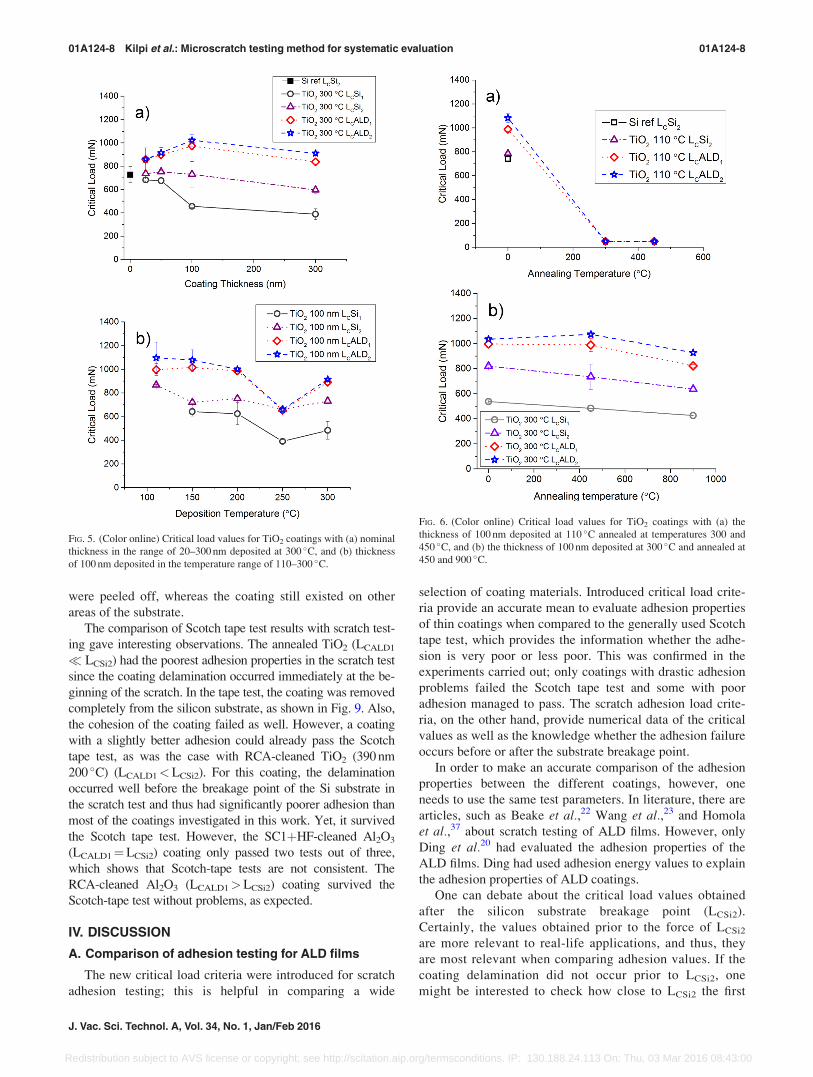
C. TiO2 coating
The critical loads of ALD TiO2 coatings are presented in
Figs. 5 and 6. The adhesion between the silicon and TiO2
was good as the first observed delamination took place after
the breakage point of silicon substrate. The only exception
was 390 nm thick ALD TiO2 deposited at 200 �C for which
the coating delamination occurred at an early stage (with
LCALD2¼ 165 mN) of the test (see Table III). This might
occur due to high stress and very large (even over 500 nm)
crystals.36
Good adhesion performance remained after annealing for
the TiO2 coatings deposited in 300 �C. Similar to Al2O3, the
annealing treatment slightly lowered the adhesion values.
However, in the two samples deposited at 110 �C, the adhe-
sion failed as the delamination occurred instantly at the
beginning of the scratch test.
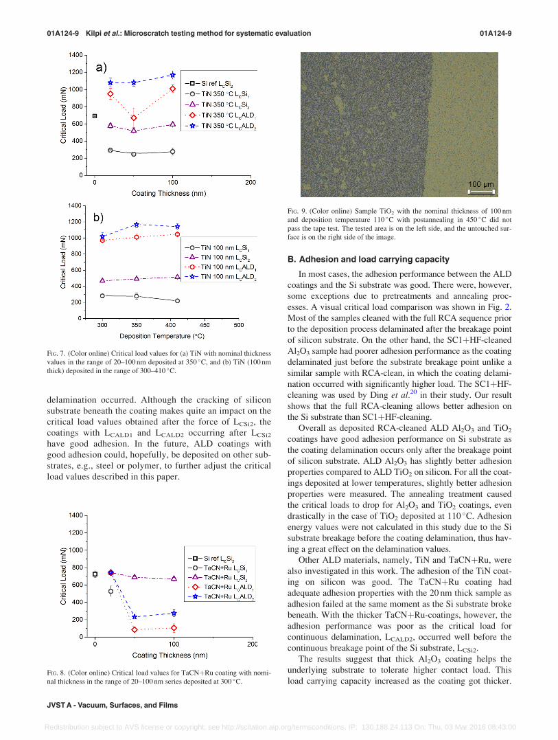
D. TiN coating
The influence of deposition temperature and coating thick-
ness on the critical loads of TiN are presented in Figs. 7(a)
and 7(b). Overall, adhesion of TiN on Si substrate was good.
The load carrying capacity of the silicon substrate, however,
decreased slightly due to deposition as the LCSi2 was lower
than the one of uncoated Si substrate.
E. TaCN1Ru coating
The impact of deposition temperature and coating thick-
ness on the critical loads of TaCNþRu coating are presented
in Fig. 8. Especially with increasing coating thickness, the
TABLE IV. Critical load values with standard deviations for TiN and TaCNþRu coated systems with different coating thicknesses, deposition parameters, and
postannealing temperatures. The RCA-cleaning was used prior to deposition.
Series Coating material Thickness (nm) Growth T ( �C) LCSi1 (mN) LCSi2 (mN) LCALD1 (mN) LCALD2 (mN)
Si (Ref. 4) — — — 443 6 2 690 6 2 — —
Thickness TiN 23.0 350 293 6 9 577 6 28 950 6 64 1081 6 65
Thickness TiN 59.5 350 246 6 3 519 6 10 671 6 113 1081 6 52
Thickness and temperature TiN 113 6 3 350 277 6 39 493 6 21 1011 6 42 1169 6 41
Temperature TiN 113 6 3 300 281 6 15 468 6 17 971 6 10 1019 6 46
Temperature TiN 90 6 3 410 219 6 26 515 6 24 1046 6 9 1143 6 34
Si (Ref. 5) — — — 613 6 73 724 6 37 — —
Thickness TaCNþRu (1)þ 19.9 — 528 6 60 743 6 35 743 6 35 743 6 35
Thickness TaCNþRu (1)þ 47.7 — — 687 6 6 85 6 22 234 6 1
Thickness TaCNþRu (1)þ 100 — — 670 6 15 106 6 53 275 6 38
01A124-6 Kilpi et al.: Microscratch testing method for systematic evaluation 01A124-6
J. Vac. Sci. Technol. A, Vol. 34, No. 1, Jan/Feb 2016
Redistribution subject to AVS license or copyright; see http://scitation.aip.org/termsconditions. IP: 130.188.24.113 On: Thu, 03 Mar 2016 08:43:00

adhesion was poor, as LCALD2 occurs at a substantially lower
load than LCSi2.
F. Scotch tape testing
The adhesion performance of the samples: RCA-cleaned
Al2O3 (300 nm 300 �C), SC1þHF cleaned Al2O3
(300 nm 300 �C), RCA-cleaned TiO2 (390 nm 200 �C), and
RCA-cleaned TiO2 (100 nm 110 �C) samples annealed at 300
and 450 �C were evaluated also using Scotch tape testing.
The results are presented in Tables II–IV. The RCA-cleaned
nonannealed Al2O3 and TiO2 samples passed all three tests,
and the coating was still adhered on the Si substrate after the
rapid tape removal from the top of the coating. SC1þHF-
cleaned Al2O3 passed the test two times out of three. The
annealed TiO2 samples failed all three tests as the coating
was removed from the tested area. In Fig. 9, for the TiO2
sample deposited at 110 �C and annealed at 450 �C, the adhe-
sion failed. The coating areas, where the tape had a contact,
FIG. 4. (Color online) Critical load values for Al2O3 films (100 nm) (a) de-
posited at 110 �C and annealed in the temperature range of 300–900 �C, (b)
deposited at 200 �C and annealed at 700 �C, and (c) deposited at 300 �C and
annealed in the temperature range of 300–900 �C.
FIG. 3. (Color online) Critical load values for (a) Al2O3 films with different
nominal coating thicknesses deposited at 300 �C, (b) Al2O3 (100 nm) depos-
ited in the range of 30–110 �C, and (c) Al2O3 (300 nm) deposited in the
range of 110–300 �C.
01A124-7 Kilpi et al.: Microscratch testing method for systematic evaluation 01A124-7
JVST A - Vacuum, Surfaces, and Films
Redistribution subject to AVS license or copyright; see http://scitation.aip.org/termsconditions. IP: 130.188.24.113 On: Thu, 03 Mar 2016 08:43:00
were peeled off, whereas the coating still existed on other
areas of the substrate.
The comparison of Scotch tape test results with scratch test-
ing gave interesting observations. The annealed TiO2 (LCALD1
� LCSi2) had the poorest adhesion properties in the scratch test
since the coating delamination occurred immediately at the be-
ginning of the scratch. In the tape test, the coating was removed
completely from the silicon substrate, as shown in Fig. 9. Also,
the cohesion of the coating failed as well. However, a coating
with a slightly better adhesion could already pass the Scotch
tape test, as was the case with RCA-cleaned TiO2 (390 nm
200 �C) (LCALD1<LCSi2). For this coating, the delamination
occurred well before the breakage point of the Si substrate in
the scratch test and thus had significantly poorer adhesion than
most of the coatings investigated in this work. Yet, it survived
the Scotch tape test. However, the SC1þHF-cleaned Al2O3
(LCALD1¼LCSi2) coating only passed two tests out of three,
which shows that Scotch-tape tests are not consistent. The
RCA-cleaned Al2O3 (LCALD1>LCSi2) coating survived the
Scotch-tape test without problems, as expected.
IV. DISCUSSION
A. Comparison of adhesion testing for ALD films
The new critical load criteria were introduced for scratch
adhesion testing; this is helpful in comparing a wide
selection of coating materials. Introduced critical load crite-
ria provide an accurate mean to evaluate adhesion properties
of thin coatings when compared to the generally used Scotch
tape test, which provides the information whether the adhe-
sion is very poor or less poor. This was confirmed in the
experiments carried out; only coatings with drastic adhesion
problems failed the Scotch tape test and some with poor
adhesion managed to pass. The scratch adhesion load crite-
ria, on the other hand, provide numerical data of the critical
values as well as the knowledge whether the adhesion failure
occurs before or after the substrate breakage point.
In order to make an accurate comparison of the adhesion
properties between the different coatings, however, one
needs to use the same test parameters. In literature, there are
articles, such as Beake et al.,22 Wang et al.,23 and Homola
et al.,37 about scratch testing of ALD films. However, only
Ding et al.20 had evaluated the adhesion properties of the
ALD films. Ding had used adhesion energy values to explain
the adhesion properties of ALD coatings.
One can debate about the critical load values obtained
after the silicon substrate breakage point (LCSi2).
Certainly, the values obtained prior to the force of LCSi2
are more relevant to real-life applications, and thus, they
are most relevant when comparing adhesion values. If the
coating delamination did not occur prior to LCSi2, one
might be interested to check how close to LCSi2 the first
FIG. 5. (Color online) Critical load values for TiO2 coatings with (a) nominal
thickness in the range of 20–300 nm deposited at 300 �C, and (b) thickness
of 100 nm deposited in the temperature range of 110–300 �C.
FIG. 6. (Color online) Critical load values for TiO2 coatings with (a) the
thickness of 100 nm deposited at 110 �C annealed at temperatures 300 and
450 �C, and (b) the thickness of 100 nm deposited at 300 �C and annealed at
450 and 900 �C.
01A124-8 Kilpi et al.: Microscratch testing method for systematic evaluation 01A124-8
J. Vac. Sci. Technol. A, Vol. 34, No. 1, Jan/Feb 2016
Redistribution subject to AVS license or copyright; see http://scitation.aip.org/termsconditions. IP: 130.188.24.113 On: Thu, 03 Mar 2016 08:43:00
delamination occurred. Although the cracking of silicon
substrate beneath the coating makes quite an impact on the
critical load values obtained after the force of LCSi2, the
coatings with LCALD1 and LCALD2 occurring after LCSi2
have good adhesion. In the future, ALD coatings with
good adhesion could, hopefully, be deposited on other sub-
strates, e.g., steel or polymer, to further adjust the critical
load values described in this paper.
B. Adhesion and load carrying capacity
In most cases, the adhesion performance between the ALD
coatings and the Si substrate was good. There were, however,
some exceptions due to pretreatments and annealing proc-
esses. A visual critical load comparison was shown in Fig. 2.
Most of the samples cleaned with the full RCA sequence prior
to the deposition process delaminated after the breakage point
of silicon substrate. On the other hand, the SC1þHF-cleaned
Al2O3 sample had poorer adhesion performance as the coating
delaminated just before the substrate breakage point unlike a
similar sample with RCA-clean, in which the coating delami-
nation occurred with significantly higher load. The SC1þHF-
cleaning was used by Ding et al.20 in their study. Our result
shows that the full RCA-cleaning allows better adhesion on
the Si substrate than SC1þHF-cleaning.
Overall as deposited RCA-cleaned ALD Al2O3 and TiO2
coatings have good adhesion performance on Si substrate as
the coating delamination occurs only after the breakage point
of silicon substrate. ALD Al2O3 has slightly better adhesion
properties compared to ALD TiO2 on silicon. For all the coat-
ings deposited at lower temperatures, slightly better adhesion
properties were measured. The annealing treatment caused
the critical loads to drop for Al2O3 and TiO2 coatings, even
drastically in the case of TiO2 deposited at 110 �C. Adhesion
energy values were not calculated in this study due to the Si
substrate breakage before the coating delamination, thus hav-
ing a great effect on the delamination values.
Other ALD materials, namely, TiN and TaCNþRu, were
also investigated in this work. The adhesion of the TiN coat-
ing on silicon was good. The TaCNþRu coating had
adequate adhesion properties with the 20 nm thick sample as
adhesion failed at the same moment as the Si substrate broke
beneath. With the thicker TaCNþRu-coatings, however, the
adhesion performance was poor as the critical load for
continuous delamination, LCALD2, occurred well before the
continuous breakage point of the Si substrate, LCSi2.
The results suggest that thick Al2O3 coating helps the
underlying substrate to tolerate higher contact load. This
load carrying capacity increased as the coating got thicker.FIG. 8. (Color online) Critical load values for TaCNþRu coating with nomi-
nal thickness in the range of 20–100 nm series deposited at 300 �C.
FIG. 9. (Color online) Sample TiO2 with the nominal thickness of 100 nm
and deposition temperature 110 �C with postannealing in 450 �C did not
pass the tape test. The tested area is on the left side, and the untouched sur-
face is on the right side of the image.
FIG. 7. (Color online) Critical load values for (a) TiN with nominal thickness
values in the range of 20–100 nm deposited at 350 �C, and (b) TiN (100 nm
thick) deposited in the range of 300–410 �C.
01A124-9 Kilpi et al.: Microscratch testing method for systematic evaluation 01A124-9
JVST A - Vacuum, Surfaces, and Films
Redistribution subject to AVS license or copyright; see http://scitation.aip.org/termsconditions. IP: 130.188.24.113 On: Thu, 03 Mar 2016 08:43:00

The difference in the critical load for the Si substrate break-
age with and without one of these coatings with 300 nm was
rather significant: LCSi2 for plain Si was around 700 mN,
whereas for Al2O3 coated Si, it was close to 1100 mN. This
behavior is beneficial for some Si based systems to provide
better endurance in the application combined with the adhe-
sion benefit as well.
In the case of TiN and thin Al2O3, the load carrying
capacity of the silicon substrate, however, decreased slightly
due to deposition as the LCSi2 of the coated system is lower
than that of uncoated Si. The reason for this is likely the
high stresses occurring on the surface of the coating system
due to deposition. Possibly for the same reason the adhesion
of the TaCNþRu coating shows poor results, especially with
increasing thickness. The high stress may be the reason for
the sudden adhesion failure occurring to the annealed TiO2
coating deposited at 110 �C, causing spontaneous delamina-
tion. The change of temperature from 110 �C to over 300 �Ccauses the crystal structure of TiO2 to change from amor-
phous to crystalline, and, thus, increases the stress in the
coating during the annealing process.
V. CONCLUSIONS
The scratch test method is widely used for adhesion eval-
uation of thin films and coatings. The results presented here
suggested that the Scotch tape test does not provide enough
information about the adhesion performance between the
coating and the substrate, especially for the more demanding
applications. However, the critical loads described in the
standard on scratch testing were not directly applicable for
ALD films. In this study, the bases for critical load evalua-
tion by scratch testing were established, and the critical loads
suitable for the ALD coating adhesion evaluation were deter-
mined as LCSi1, LCSi2, LCALD1, and LCALD2, representing the
failure points of the silicon substrate and the coating delami-
nation points of the ALD coating. This approach was sug-
gested for adhesion evaluation of the ALD layers on silicon.
The adhesion performance of the ALD Al2O3, TiO2, TiN,
and TaCNþRu coatings with thicknesses ranging between 20
and 600 nm and deposition temperature between 30 and
410 �C on silicon wafers was investigated. In addition, the
impact of the annealing process after deposition on adhesion
was evaluated. The test results carried out using the scratch
test showed that the coating deposition and annealing temper-
ature, the thickness of the coating, and the surface pretreat-
ments of the Si wafer all had an impact on the adhesion
performance of the ALD coatings on the silicon wafer.
Coating delamination occurred shortly after the breakage
point of silicon in most cases. The best adhesion performance
was measured for Al2O3 coatings on silicon. The adhesion
between the ALD coatings and silicon substrate was generally
good. The adhesion properties became slightly poorer after
annealing the coatings at elevated temperatures. The coatings
deposited on RCA-cleaned samples had better adhesion com-
pared to the SC1þHF-cleaned sample. There was also
improved load carrying capacity due to the coating thickness
and deposition temperature, especially in the case of the ALD
Al2O3. The results show that the scratch test is a useful and
applicable tool for adhesion evaluation of the ALD deposited
coatings, even done for the thin (20 nm) coatings.
ACKNOWLEDGMENTS
The authors are grateful for Tekes and private funding by
ASM Microchemistry Oy, Beneq Oy, Murata Electronics
Oy, Picosun Oy, Okmetic Oyj, and Oxford Instruments
Analytical Oy through the MECHALD Project. Special
thanks also to Saima Ali and Timo Sajavaara for their
contribution concerning XRR and low temperature ALD
Al2O3 coating manufacturing, respectively. This work is
linked to the Finnish Centers of Excellence in Atomic Layer
Deposition (ref. 251220).
1R. L. Puurunen, J. Appl. Phys. 97, 121301 (2005).2M. Ritala and M. Leskel€a, Handbook of Thin Film Materials, edited by H.
S. Nalwa (Academic, San Diego, CA, 2001), Vol. 1, pp. 103–159.3S. M. George, Chem. Rev. 110, 111 (2009).4F. Buja, G. Fiorentino, J. Kokorian, and W. M. Spengen, Nanotechnology
26, 255701 (2015).5R. L. Puurunen, H. Kattelus, and T. Suntola, Handbook of Silicon BasedMEMs Materials and Technologies, edited by V. Lindroos, M. Tilli, A.
Lehto, and T. Motooka (Elsevier, Oxford, 2010), pp. 433–446.6F. Gao, S. Arpiainen, and R. L. Puurunen, J. Vac. Sci. Technol. A 33,
010601 (2015).7T. M. Mayer, J. W. Elam, S. M. George, P. G. Kotula, and R. S. Goeke,
Appl. Phys. Lett. 82, 2883 (2003).8N. D. Hoivik, J. W. Elam, R. J. Linderman, V. M. Bright, S. M. George,
and Y. C. Lee, Sens. Actuators A 103, 100 (2003).9C. F. Herrmann, F. W. DelRio, D. C. Miller, S. M. George, V. M. Bright,
J. L. Ebel, R. E. Strawser, R. Cortez, and K. D. Leedy, Sens. Actuators A
135, 262 (2007).10T. W. Scharf, S. V. Prasad, T. M. Mayer, R. S. Goeke, and M. T. Dugger,
J. Mater. Res. 19, 3443 (2004).11J. Kyyn€ar€ainen et al., Sens. Lett. 5, 126 (2007).12R. L. Puurunen, J. Saarilahti, and H. Kattelus, ECS Trans. 11, 3 (2007).13M. Blomberg, H. Kattelus, and A. Miranto, Sens. Actuators A 162, 184
(2010).14A. Rissanen, U. Kantoj€arvi, M. Blomberg, J. Antila, and S. Er€anen, Sens.
Actuators A 182, 130 (2012).15R. L. Puurunen et al., Sens. Actuators A 188, 240 (2012).16B. D. Davidson, D. Seghete, S. M. George, and V. M. Bright, Sens.
Actuators A 166, 269 (2011).17S. T. Gonczy and N. Randall, Int. J. Appl. Ceram. Technol. 2, 422 (2005).18K. L. Mittal, Electrocomponent Sci. Technol. 3, 21 (1976).19J. Meneve et al., Adhesion Measurement of Films and Coatings, edited by
K. L. Mittal (VSP BV, The Netherlands, 2001), Vol. 2, pp. 79–106.20J. N. Ding, X. F. Wang, N. Y. Yuan, C. L. Li, Y. Y. Zhu, and B. Kan,
Surf. Coat. Technol. 205, 2846 (2011).21O. M. E. Ylivaara et al., Thin Solid Films 552, 124 (2014).22B. D. Beake, M. I. Davies, T. W. Liskiewicz, V. M. Vishnyakov, and S. R.
Goodes, Wear 301, 575 (2013).23W. K. Wang, H. C. Wen, C. H. Cheng, W. C. Chou, W. H. Yau, C. H.
Hung, and C. P. Chou, J. Phys. Chem. Solids 75, 334 (2014).24S. J. Bull, Tribol. Int. 30, 491 (1997).25Y. Xie and H. M. Hawthorne, Surf. Coat. Technol. 155, 121 (2002).26S. J. Bull and E. G. Berasetegui, Tribol. Int. 39, 99 (2006).27W. Kern, Handbook of Semiconductor Wafer Cleaning Technology -
Science, Technology, and Applications, edited by W. Kern (William
Andrew/Noyes, Westwood, NJ, 1993), pp. 1–67.28B. Vermang, H. Goverde, A. Uruena, A. Lorenz, E. Cornagliotti, A.
Rothschild, J. John, J. Poortmans, and R. Mertens, Sol. Energy Mater Sol.
Cells 101, 204 (2012).29R. L. Puurunen, J. Kiiham€aki, and H. Kattelus, “Controlling the solubility
of ALD aluminium oxide in deionised water,” Poster presented at the
AVS ALD 2005 Conference (2005).30K. N. Stoev and K. Sakurai, Spectrochim. Acta B 54, 41 (1999).
01A124-10 Kilpi et al.: Microscratch testing method for systematic evaluation 01A124-10
J. Vac. Sci. Technol. A, Vol. 34, No. 1, Jan/Feb 2016
Redistribution subject to AVS license or copyright; see http://scitation.aip.org/termsconditions. IP: 130.188.24.113 On: Thu, 03 Mar 2016 08:43:00

31S. Sintonen, A. Saima, O. M. E. Ylivaara, R. L. Puurunen, and H.
Lipsanen, J. Vac. Sci. Technol. A 32, 01A111 (2014).32L. G. Parratt, Phys. Rev. 95, 359 (1954).33C1624-05, Standard Test Method for Adhesion Strength and Mechanical
Failure Modes of Ceramic Coatings by Quantitative Single Point ScratchTesting (West Conshohocken, PA, 2015), p. 28.
34G. M. Pharr, W. C. Oliver, and D. S. Harding, J. Mater. Res. 6, 1129 (1991).
35V. Domnich and Y. Gogotsi, Rev. Adv. Mater. Sci. 3, 1 (2002).36R. L. Puurunen, T. Sajavaara, E. Santala, V. Miikkulainen, T. Saukkonen,
M. Laitinen, and M. Leskel€a, J. Nanosci. Nanotechnol. 11, 8101 (2011).37T. Homola, V. Bur�s�ıkov�a, T. V. Ivanova, P. Soucek, P. S. Maydannik,
D. C. Cameron, and J. M. Lackner, “Mechanical properties of atomic
layer deposited Al2O3/ZnO nanolaminates,” Surf. Coat. Technol. (in
press).
01A124-11 Kilpi et al.: Microscratch testing method for systematic evaluation 01A124-11
JVST A - Vacuum, Surfaces, and Films
Redistribution subject to AVS license or copyright; see http://scitation.aip.org/termsconditions. IP: 130.188.24.113 On: Thu, 03 Mar 2016 08:43:00