Thin Film Mechanics - mrsec.harvard.edu · B. Stress generation due to coalescence of grain...
26
Thin Film Mechanics Joost Vlassak DEAS Harvard University AP 298r Spring 2004
Transcript of Thin Film Mechanics - mrsec.harvard.edu · B. Stress generation due to coalescence of grain...

Thin Film Mechanics
Joost Vlassak
DEAS Harvard University
AP 298r Spring 2004

OVERVIEW
1. Origin of residual stresses in thin films
• Epitaxial stresses
• Thermal stresses
• Intrinsic or growth stresses
- surface stress effects
- crystallite coalescence
- grain growth
- vacancy annihilation
- effect of impurities
- effect of phase transformations
- stresses in sputtered films
2. Deformation processes in thin films
• Grain boundary diffusion controlled creep
• Dislocation mechanisms

1. Origin of residual stresses in thin films 1. Epitaxial stresses Epitaxial stresses arise when films have perfectly coherent interfaces with their substrates, i.e., when the crystal lattices in film and substrates line up perfectly.
as
af
σmf σmf
e.g. Cubic on cubic: Fe on GaAS, AlAs on GaAS Cubic on hcp: 111 plane in cubic film on (0001) plane in hcp crystal Assuming enough symmetry, the misfit strain is given by:
εxx = ε yy =as − a f
a f= ε mf
The epitaxial strain gives rise to a misfit stress, σmf, in the film. Since the film is a single crystal, one has to use anistropic elasticity to calculate the misfit stress.

Example: Consider a film with cubic crystal structure and with the 001 planes parallel to the 001 planes of a cubic substrate. Hook’s law for a cubic material:
σ xx
σ yy
σ zz
⎡
⎣
⎢ ⎢ ⎢
⎤
⎦
⎥ ⎥ ⎥
=C11 C12 C12
C12 C11 C12
C12 C12 C11
⎡
⎣
⎢ ⎢ ⎢
⎤
⎦
⎥ ⎥ ⎥
ε xx
ε yy
εzz
⎡
⎣
⎢ ⎢ ⎢
⎤
⎦
⎥ ⎥ ⎥
e x || [100]e y || [010]e z || [001]
But the film is in plane stress: σ z = 0 or
2C12εmf + C11εzz = 0
The misfit stress in a film with the 001 plane parallel to the substrate is
σ mf = C11 + C12 −2C12
2
C11
⎡
⎣ ⎢ ⎢
⎤
⎦ ⎥ ⎥ εmf
εzz = −2C12C11
εmf
The biaxial modulus for the 100 plane is then
M100 = C11 + C12 −2C12
2
C11
For films with the 111) plane parallel to the substrate:
σ mf =6C44 C11 + 2C12( )C11 + 2C12 + 4C44
εmf
εzz = −2C11 + 4C12 − 4C44C11 + 2C12 + 4C44
ε mf

The expression εmf = as − af( ) af only holds when the film is sufficiently thin so that the film assumes the lattice parameter of the substrate. When the film thickness increases, it becomes energetically favorable for misfit dislocation at the interface between film and substrate to reduce the stress in the film.
Strain in film:
ε = εmf −bs
•Strain energy per unit area:
Es = M ε mf −bs
⎛ ⎝
⎞ ⎠
2t
•Dislocation energy per unit length:
E / l =b2
4π 1 −ν( )2µ f µs
µ f + µs( )lnβtb
⎛ ⎝
⎞ ⎠ β = constant
l = dislocation length per unit area = 2/s for a square array of edge dislocations:
l =2ss 2 =
2s
⇒ Etot = Mt ε mf −
bs
⎛ ⎝
⎞ ⎠
2+
2b2
4π 1 − ν( )s2µ f µs
µ f + µsn
βtb
⎛ ⎝
⎞ ⎠
S
t

Misfit dislocation will form, if the energy is decreased by doing so:
dEtotd b / s( ) b/s=0
< 0
Thus the critical thickness at which it becomes favorable to form misfit dislocations:
tc
ln βtcb
⎛ ⎝
⎞ ⎠
=2µ f µ s
µ f + µ s
b4π 1 − ν( )Mε mf
(Matthews)
If t < tc : Misfit dislocations are not stable and will not form. If t > tc : Misfit dislocations are stable, but do not necessarily form
(metastable state). 2. Thermal stress When a film on a substrate is subjected to a temperature change, differential thermal expansion will result in thermal stresses in film and substrate. For an infinitely deep substrate:
σT = ∆αMdTTo
Tf
∫ = ∆α M∆T
=E
1−ν( )∆α ∆T
where:
- ∆α =1
∆T∆αdT
To
T f
∫ = average, differential thermal expansion
coefficient.
- M =E
1 − ν for isotropic materials
-We assumed only elastic deformation.

3. Intrinsic or growth stresses It is often observed that stresses develop in films during deposition or growth. These stresses are not due to lattice mismatch or thermal mismatch strains and are therefore called intrinsic stresses or growth stresses. These stresses arise because generally films are deposited under non-equilibrium conditions. In general, any redistribution of matter will result in film stresses, since the film is constrained by the substrate Typical behavior of the average film stress as a function of film thickness is shown in the following figure:
σRelaxation, incorporation of
extra atoms at ledges and GB
= f(T)
Tension due to crystallite coalescence
Compression due to surface stress effects
Film thickness t

A. Surface stress effects (Important for very thin films ~ islands) Note: Difference between surface energy and surface stress for solids. • Surface energy γ: Reversible work required to create a unit area of a
surface at constant temperature, volume and chemical potential.
• Surface stress fij: Force per unit length of exposed edge that must be
applied to a terminating surface in order to keep it in equilibrium. i = direction normal to the exposed edge j = direction of the force
(Vermaak et al., Surface Science, 12, 128-133 (1968)). The relationship between surface stress and energy is:
fij = γδ ij +∂γ
∂ε ij or f = γ +
∂γ∂ε
(isotropic surface)
The derivative of γ arises from the elastic stretching of the surface, which is only possible for a solid. For a fluid we cannot stretch the surface elastically and the derivative is zero. In that case fij = γ . The surface stress f causes the pressure inside a small solid crystallite to be larger than the outside pressure. The pressure difference is called the Laplace pressure.

Consider a small island of the film material on a substrate:
f = surface stress of
crystallite surface g = surface stress of side wall h = surface stress of interface (After R. Cammarata)
From a simple equilibrium of forces, we find:
∆pr =gr
+f + h
t (in the plane of the film)
∆pz =2gr
(normal to the film)
Therefore, the initial equilibrium strain inside a small crystallite is
εr =1−ν
Ef + h( ) t + g r[ ]
Initially, a small crystallite will have an equilibrium lattice parameter < af. However, as the crystallite grows the equilibrium lattice parameter increases to af. Since the crystallite is constrained by the substrate at this point, a compressive stress is generated in the film.
t
f
g
h
po
2r
pr pz,
Film Crystallite
Substrate

B. Stress generation due to coalescence of grain boundaries The "grain boundary relaxation" model by Hoffman, R. W. Hoffman, Phys. Thin Films, 3, 211 (1968) R. W. Hoffman, Phys. Thin Films, 34, 185 (1976) In the early stages of film growth, the film consists of small crystallites. When these crystallites coalesce, a tensile stress is generated. As crystallites grow, the gap between them decreases, until it is so small that cohesion begins to develop between the crystallites. At some points, the interactions between the crystallites is strong enough to close the gap by elastic deformation of the crystallites. The following analysis is due to Freund and Chason: (J. of Appl. Phys., 89, 4866, 2001).
The JKR analysis of contacting spheres leads to the following expression for the force between two contacting spheres with surface energy γ, and fixed in space is:
P =4π3
Rγ , γ = γ s −12
γ GB ,
and the average stress in a film of thickness tc at contact:
σ ave =4γR
=2πγ3tc
,
Isolated crystallies
Before coalescence Substrate
R
After coalescence
σ σ

Figure 7 Freund paper Conclusions: • Stresses in small crystallites can be quite high. • The stress calculated in the model is an upper bound since:
-The resistance to deformation of the substrate is ignored. -Stress relaxation due to diffusion over the surface of the islands is ignored.
-Island coalescence does not occur everywhere simultaneously.

Fig. 4 from Aberman
No relaxation
Stress is frozen in.
Stress relaxes
during subsequent
growth
Low ad-atom mobility: Low temperature
High ad-atom mobility: High temperature
Vapor flux
σ σ
Stress free
σ σ

C. Stress generation due to grain growth. After P. Chaudhari, J. Vac. Sc. Tech., 9, 520 (1972). Grain boundaries are less dense than the grain lattice. Therefore, elimination of grain boundaries leads to a densification of the film and to tensile stresses in it. - Assume we have spherical grains of diameter L. - Assume the excess volume per unit of grain boundary is given by ∆a . Consider the following though experiment:
1. Stress-free film with grain size Lo. 2. Detach film from substrate. 3. Allow grain growth. 4. Elastically strain the film to make
it fit on the substrate. The grain boundary area per unit volume of film material is
σ σ

A =12
4πr 2
4 3( )πr 3 =3
2r=
3L
The excess volume per unit volume due to grain boundaries is then given by:
V xs =3L
∆a
Thus, if a film is initially deposited with grain size Lo and the grain size increases to L, it undergoes a volumetric strain relative to the as-deposited state of:
∆V xs = 3∆a1L
−1Lo
⎛ ⎝ ⎜
⎞ ⎠ ⎟
The volumetric strain results in in-plane strains:
ε xx = ε yy = −13
∆V xs = ∆a1Lo
−1L
⎛ ⎝ ⎜
⎞ ⎠ ⎟
and stresses:
σ xx = σ yy =E
1 − ν∆a
1Lo
−1L
⎛ ⎝ ⎜
⎞ ⎠ ⎟
Reduction of grain boundary area provides a driving force for grain growth. On the other hand, grain growth results in increased film stress and strain energy. The total energy in a unit volume of film material due to grain boundaries and film stress is:
E =3L
γ GB +1 − ν2E
σ xx2 + σ yy
2( )=3L
γ GB +E
1 − ν∆a 2 1
Lo−
1L
⎛ ⎝ ⎜
⎞ ⎠ ⎟
2
Grain growth will stop when dE = 0:
−3γ GB + 2∆a 2 E1 − ν
1Lo
−1L
⎛ ⎝ ⎜
⎞ ⎠ ⎟ = 0
or when: 1Lo
−1L
=3 1 − ν( )γ GB
2E∆a2 & σ =3γ GB2∆a
Example:

γ GB ~ 0.3J / m2
∆a ~ 10−10 m
⎫ ⎬ ⎪
⎭ ⎪ → σ ~ 5 GPa
Figure 22 from D. S. Gardner et al.

D. Stress generation due to excess vacancy annihilation When a film is deposited at low temperature, there is very little surface diffusion and one would expect the vacancy concentration to be much larger than at equilibrium. When these excess vacancies are subsequently annihilated, the associated volume change results in a stress in the film. The stress change depends on: • Vacancy volume Ωv • Site of annihilation
- free surface - interface film-substrate - grain boundaries - edge dislocations
What stress change can we expect?
-Every time a vacancy annihilates, a volume expansion Ω − Ωv takes place.
-If ∆C vacancies are annihilated per unit volume, then the total volumetric strain in the film is ∆e = ∆C Ω − Ωv( ).
The associated in-plane stains and stresses are:
ε xx = ε yy = −∆e3
= −∆C3
Ω − Ωv( )
σ xx = σ yy = −E
3 1 − ν( ) ∆C Ω − Ωv( )
Ω
Ωv

Depending on where the vacancy is annihilated, an additional stress component may develop: 1. Free surface or interface: no additional stress since the in-plane
dimensions of the film are not changed 2. Grain boundaries: a) Vertical boundary
Annihilation at a vertical boundary results in an in-plane change of film dimensions. A tensile stress develops.
b) Horizontal boundary
Annihilation at a horizontal grain boundary does not result in stress.
3. Edge dislocation
Annihilation of vacancies at an edge dislocation makes the edge dislocation climb: - If b || film: tensile stress develops - If b ⊥ film: no stress develops

Vacancy annihilation at Grain Boundaries
figure 12 From Nix et al.
From this result, it seems unlikely that vacancy annihilation contributes significantly to stress generation for low temperature deposition.
E. Impurity effects - The effect of impurities is not very well understood - Oxygen usually has the most significant effect on stress in metal films
and tends to reduce tensile stress. The next figure shows the effect of O2 on the residual stress in silver films.
not simple.

From Aberman and Koch, Thin solid Films 66, 217, 1980
F. Effect of phase transformation Phase transformations often result in volume changes, and hence, stress changes:
Figure (Stress temp behavior)
Figure

G. Stresses in sputtered films Good review in G. Windischmann, CRC Crit. Rev. in Solid State and Mat. Sc., 17, 574 (1992). Based on work by J. Thornton, D. Hoffman, Thin Solid Films, 171, 5-31 (1989). - Most of the mechanisms discussed so far, involve densification of the
film in one form or another. Therefore, they naturally lead to tensile stresses in deposited films.
- In sputtered films very large compressive stresses can be observed. These stresses are caused by “atomic shot peening”.
Sputtering
O+
O+
plasmasubstrate
cathode(target material)
Main variables: - Sputtering gas pressure (e.g., Ar pressure). Low pressure increases the
mean free path length of neutralized reflected ions. - Ratio of molecular masses of target and sputtering ions.
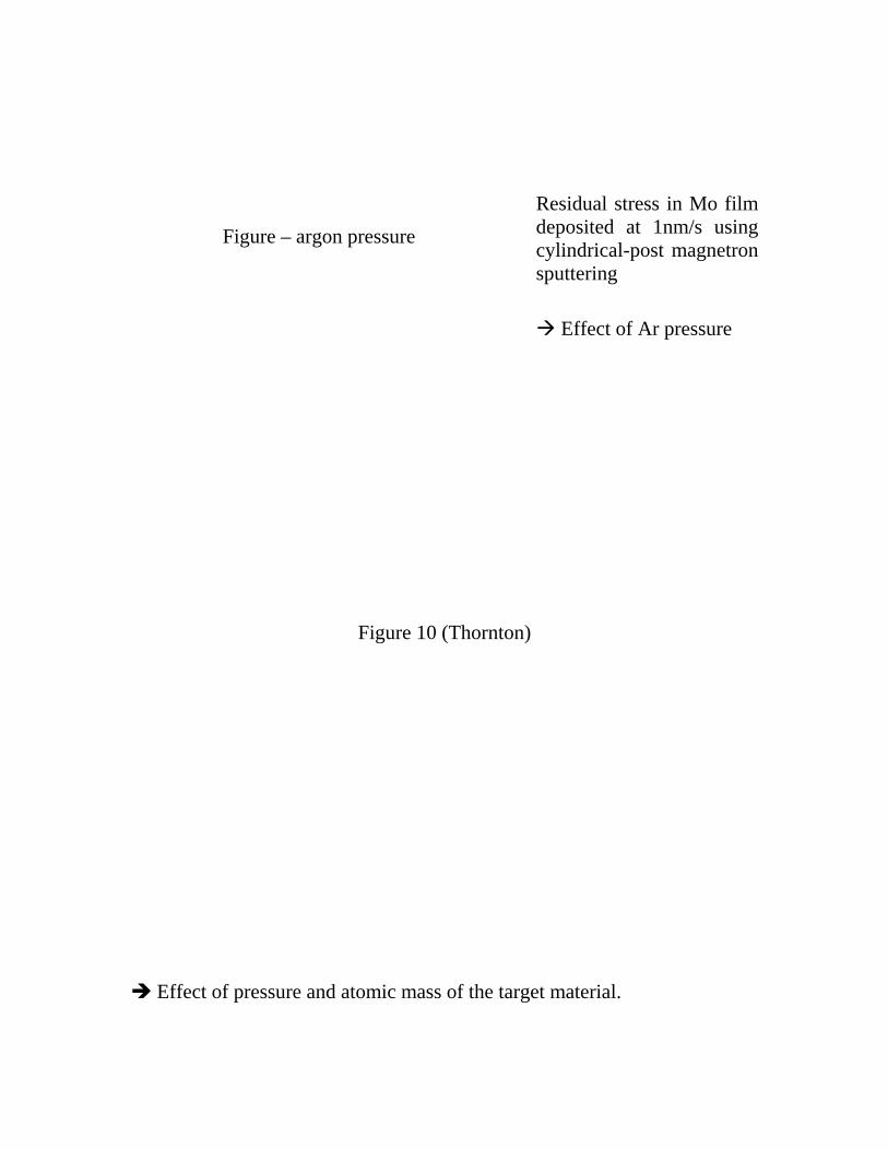
Residual stress in Mo film deposited at 1nm/s using cylindrical-post magnetron sputtering
Effect of Ar pressure
Figure 10 (Thornton)
Effect of pressure and atomic mass of the target material.
Figure – argon pressure

Effects of Mtarget/ Mgas and of sputtering geometry

2. Deformation processes in thin films
Deformation mechanism map Deformation mechanisms maps need to be modified to account for the special microstructure of thin films. A. Grain boundary diffusion controlled creep Freestanding films
Ý ε = 3DGBδGBΩσ
kTLh2
L: Grain size h: Film thickness
Films on substrates
σGB t( ) = σ o exp −λtto
⎛ ⎝ ⎜
⎞ ⎠ ⎟
with to =4π 1 − ν 2( )kBTh3
E f δDGBΩ
λ = 8.10 + 30.65 h / L( )
σ σ
Thouless, Acta Met. Mat. 41, 1057
σ σ
Substrate

B. Plastic deformation through dislocation glide z
y
x
Oxide
Film
Substrate
h
N
b
λ ϕ
Biaxial stress σ
The following is a model for plasticity in metal films by W. D. Nix. Assume that the grain size is much larger than the film thickness and that the film has a passivating oxide of thickness t. - Work done to move the dislocation a unit length
W1 = τbh
sinϕ= σhb
cosϕ cos λsinϕ
- Work done to lay down two dislocations, one at the interface with the substrate, one at the interface with the passivating layer:
W2 =b2
4π 1 − ν( )2µsµ s
µ f + µ sln
β1hb
⎛ ⎝ ⎜ ⎞
⎠ ⎟ +b2
4π 1 − ν( )2µ f µ o
µ f + µoln
β2hb
⎛ ⎝ ⎜ ⎞
⎠ ⎟ ⎡
⎣ ⎢ ⎢
⎤
⎦ ⎥ ⎥
- Equating both contributions for the work, we find
σ =sinϕ
cosϕ cosλb
2π 1 − ν( )1h
µ f µs
µ f + µ sln
β1hb
⎛ ⎝ ⎜ ⎞
⎠ ⎟ +µ f µ o
µ f + µoln
β2tb
⎛ ⎝ ⎜ ⎞
⎠ ⎟ ⎡
⎣ ⎢ ⎢
⎤
⎦ ⎥ ⎥
Yield stress of film is inversely proportional to film thickness. This model ignores any effects of the Peierl's stress, grain boundaries, or interactions with other dislocation.

Data from R. Venkatraman, Ph.D. thesis Data from Kuan & Murakani

Effect of dislocation glide and grain boundary diffusion: Data from D. Weiss, Ph.D. thesis (2000):