YSZ thin films with minimized grain boundary resistivity
6
10486 | Phys. Chem. Chem. Phys., 2016, 18, 10486--10491 This journal is © the Owner Societies 2016 Cite this: Phys. Chem. Chem. Phys., 2016, 18, 10486 YSZ thin films with minimized grain boundary resistivity† Edmund M. Mills, a Matthias Kleine-Boymann, b Juergen Janek, b Hao Yang, c Nigel D. Browning, c Yayoi Takamura a and Sangtae Kim* a In recent years, interface engineering of solid electrolytes has been explored to increase their ionic conductivity and improve the performance of solid oxide fuel cells and other electrochemical power sources. It has been observed that the ionic conductivity of epitaxially grown thin films of some electrolytes is dramatically enhanced, which is often attributed to effects (e.g. strain-induced mobility changes) at the heterophase boundary with the substrate. Still largely unexplored is the possibility of manipulation of grain boundary resistivity in polycrystalline solid electrolyte films, clearly a limiting factor in their ionic conductivity. Here we report that the ionic conductivity of yttria stabilized zirconia thin films with nano-columnar grains grown on a MgO substrate nearly reaches that of the corresponding single crystal when the thickness of the films becomes less than roughly 8 nm (smaller by a factor of three at 500 1C). Using impedance spectroscopy, the grain boundary resistivity was probed as a function of film thickness. The resistivity of the grain boundaries near the film–substrate interface and film surface (within 4 nm of each) was almost entirely eliminated. This minimization of grain boundary resistivity is attributed to Mg 2+ diffusion from the MgO substrate into the YSZ grain boundaries, which is supported by time of flight secondary ion mass spectroscopy measurements. We suggest grain boundary ‘‘design’’ as an attractive method to obtain highly conductive solid electrolyte thin films. Introduction Solid oxide fuel cells (SOFCs) are electrochemical devices that convert chemical energy into electrical energy. 1 Central to SOFC operation is the electrolyte, which lies between the anode and cathode where redox half-reactions occur. In order for the fuel (e.g. H 2 ) to be oxidized at the anode, the electrolyte must allow sufficient ion diffusion so that the two half-reactions can be linked to complete the full reaction. Therefore ionic conductiv- ity is the critical material property for electrolytes. Over the past decades various approaches have been taken to improve the ionic conductivity of electrolyte materials including exploration of novel materials, compositional optimization, and more recently, interface engineering. 2 Interface engineering shows promise for improving the ionic conductivity of electrolytes and performance of SOFCs. 3,4 The local structural, electrical, and chemical properties of interfaces between two different materials, i.e. hetero-interfaces, or between two chemically identical materials, e.g. grain boundaries, deviate from those of the corresponding crystalline bulk. Consequently, the defect concentration and dynamics of ionic motion parallel to and perpendicular to the interface may be altered. For example, it has been known that in some prominent oxide- or proton- conducting solid electrolytes, ions are depleted to form a space charge region in the vicinity of the grain boundary core, leading to obstruction of ion transport across the grain boundaries and thus limiting the ionic conductivity of polycrystalline electro- lytes (frequently designated as the space charge effect). 5,6 On the other hand, interfaces may also be beneficial; considerable enhanced ionic conductivity relative to bulk materials has been observed at the hetero-interface of yttria stabilized zirconia (YSZ) thin film and a MgO substrate. 7 Extensive efforts have been made to utilize such an ‘‘enhancement’’ effect in the design of advanced electrolyte materials with high ionic conductivity, e.g. through grain boundary modification 8 or the design of composite materials. 9 In recent years, there have been multiple reports of dramatically enhanced ionic conductivity in epitaxial thin film electrolytes. 7,10,11 Different sources of this effect have been proposed, including strain, 12 misfit dislocations, 13 and disorder in the oxygen sub- lattice at the hetero-interface in thin films. 11 It has been demonstrated that strain has a sizeable effect on the ionic a University of California Davis, Department of Chemical Engineering and Materials Science, 3001 Ghausi Hall, Davis California 95616, USA. E-mail: [email protected] b Justus-Liebig-Universita¨t Gießen, Physikalisch-Chemisches Institut, Heinrich-Buff-Ring 58, 35392 Gießen, Germany c Pacific Northwest National Laboratory, 902 Battelle Boulevard, Richland, WA, USA † Electronic supplementary information (ESI) available: Whipple analysis of SIMS depth profiles. See DOI: 10.1039/c5cp08032k Received 29th December 2015, Accepted 18th March 2016 DOI: 10.1039/c5cp08032k www.rsc.org/pccp PCCP PAPER Open Access Article. Published on 31 March 2016. Downloaded on 2/15/2022 5:12:46 AM. This article is licensed under a Creative Commons Attribution 3.0 Unported Licence. View Article Online View Journal | View Issue
Transcript of YSZ thin films with minimized grain boundary resistivity

10486 | Phys. Chem. Chem. Phys., 2016, 18, 10486--10491 This journal is© the Owner Societies 2016
Cite this:Phys.Chem.Chem.Phys.,
2016, 18, 10486
YSZ thin films with minimized grain boundaryresistivity†
Edmund M. Mills,a Matthias Kleine-Boymann,b Juergen Janek,b Hao Yang,c
Nigel D. Browning,c Yayoi Takamuraa and Sangtae Kim*a
In recent years, interface engineering of solid electrolytes has been explored to increase their ionic
conductivity and improve the performance of solid oxide fuel cells and other electrochemical power
sources. It has been observed that the ionic conductivity of epitaxially grown thin films of some
electrolytes is dramatically enhanced, which is often attributed to effects (e.g. strain-induced mobility
changes) at the heterophase boundary with the substrate. Still largely unexplored is the possibility of
manipulation of grain boundary resistivity in polycrystalline solid electrolyte films, clearly a limiting factor
in their ionic conductivity. Here we report that the ionic conductivity of yttria stabilized zirconia thin
films with nano-columnar grains grown on a MgO substrate nearly reaches that of the corresponding
single crystal when the thickness of the films becomes less than roughly 8 nm (smaller by a factor of
three at 500 1C). Using impedance spectroscopy, the grain boundary resistivity was probed as a function
of film thickness. The resistivity of the grain boundaries near the film–substrate interface and film surface
(within 4 nm of each) was almost entirely eliminated. This minimization of grain boundary resistivity is
attributed to Mg2+ diffusion from the MgO substrate into the YSZ grain boundaries, which is supported
by time of flight secondary ion mass spectroscopy measurements. We suggest grain boundary ‘‘design’’
as an attractive method to obtain highly conductive solid electrolyte thin films.
Introduction
Solid oxide fuel cells (SOFCs) are electrochemical devices thatconvert chemical energy into electrical energy.1 Central to SOFCoperation is the electrolyte, which lies between the anode andcathode where redox half-reactions occur. In order for the fuel(e.g. H2) to be oxidized at the anode, the electrolyte must allowsufficient ion diffusion so that the two half-reactions can belinked to complete the full reaction. Therefore ionic conductiv-ity is the critical material property for electrolytes. Over the pastdecades various approaches have been taken to improve theionic conductivity of electrolyte materials including explorationof novel materials, compositional optimization, and morerecently, interface engineering.2
Interface engineering shows promise for improving the ionicconductivity of electrolytes and performance of SOFCs.3,4 Thelocal structural, electrical, and chemical properties of interfaces
between two different materials, i.e. hetero-interfaces, or betweentwo chemically identical materials, e.g. grain boundaries, deviatefrom those of the corresponding crystalline bulk. Consequently,the defect concentration and dynamics of ionic motion parallel toand perpendicular to the interface may be altered. For example, ithas been known that in some prominent oxide- or proton-conducting solid electrolytes, ions are depleted to form a spacecharge region in the vicinity of the grain boundary core, leadingto obstruction of ion transport across the grain boundaries andthus limiting the ionic conductivity of polycrystalline electro-lytes (frequently designated as the space charge effect).5,6 Onthe other hand, interfaces may also be beneficial; considerableenhanced ionic conductivity relative to bulk materials has beenobserved at the hetero-interface of yttria stabilized zirconia(YSZ) thin film and a MgO substrate.7 Extensive efforts havebeen made to utilize such an ‘‘enhancement’’ effect in the designof advanced electrolyte materials with high ionic conductivity,e.g. through grain boundary modification8 or the design ofcomposite materials.9
In recent years, there have been multiple reports of dramaticallyenhanced ionic conductivity in epitaxial thin film electrolytes.7,10,11
Different sources of this effect have been proposed, includingstrain,12 misfit dislocations,13 and disorder in the oxygen sub-lattice at the hetero-interface in thin films.11 It has beendemonstrated that strain has a sizeable effect on the ionic
a University of California Davis, Department of Chemical Engineering
and Materials Science, 3001 Ghausi Hall, Davis California 95616, USA.
E-mail: [email protected] Justus-Liebig-Universitat Gießen, Physikalisch-Chemisches Institut,
Heinrich-Buff-Ring 58, 35392 Gießen, Germanyc Pacific Northwest National Laboratory, 902 Battelle Boulevard, Richland, WA, USA
† Electronic supplementary information (ESI) available: Whipple analysis of SIMSdepth profiles. See DOI: 10.1039/c5cp08032k
Received 29th December 2015,Accepted 18th March 2016
DOI: 10.1039/c5cp08032k
www.rsc.org/pccp
PCCP
PAPER
Ope
n A
cces
s A
rtic
le. P
ublis
hed
on 3
1 M
arch
201
6. D
ownl
oade
d on
2/1
5/20
22 5
:12:
46 A
M.
Thi
s ar
ticle
is li
cens
ed u
nder
a C
reat
ive
Com
mon
s A
ttrib
utio
n 3.
0 U
npor
ted
Lic
ence
.
View Article OnlineView Journal | View Issue

This journal is© the Owner Societies 2016 Phys. Chem. Chem. Phys., 2016, 18, 10486--10491 | 10487
conductivity of YSZ thin films, through modifying the volumeavailable for oxygen-ion hopping, with compressive strainreducing conductivity and tensile strain enhancing it. Never-theless, due to the variety of microstructures in thin films, theeffect of other structural features and their interactions have yetto be untangled; the ionic conductivity may be modified byadditional mechanisms.14
Grain boundaries are often formed during the growth of YSZand other electrolyte thin films due to structural differencesbetween the film and substrate, leading to polycrystalline – mostlyeven nanocrystalline films.15 As these grain boundaries are highlyresistive to ionic conduction, the enhancement observed in epitaxialfilms can be nullified in polycrystalline films. Additionally, grainboundaries may relieve strain, reducing ionic conductivity enhance-ments due to strain.12 Research on the effect of grain bound-aries on the ionic conductivity of thin films has begun, forexample, examining the effect of grain orientation and grainboundary coherence on thin film ionic conductivity.16 One areayet to be explored is the intersection of grain boundaries andthe hetero-interface between the thin film and the substrate.This is of practical importance, as such intersections will berelevant when attempting to utilize the thin film interface effectin SOFCs. If the high grain boundary resistivity at this point isunaltered, it will limit the conductivity of the electrolyte andobstruct the attempt to improve the ionic conductivity.
To investigate the ionic conductivity of grain boundariesnear the hetero-interface, we synthesized YSZ thin films withnano-columnar grains and characterized their electrical proper-ties using impedance spectroscopy. The thickness was varied togain insight into the evolution of the ionic conductivity over thefilm thickness. The grain boundary resistance near the inter-face and extending approx. 8 nm into the film is almostcompletely eliminated; the thinnest nano-crystalline filmsshow ionic conductivity comparable to single crystal YSZ. Weattribute this reduction in grain boundary resistance to diffu-sion of Mg2+ from the substrate into the grain boundary cores.We us time of flight secondary ion mass spectrometry (ToF-SIMS) measurements to confirm diffusion of Mg2+ into thefilms, primarily along the grain boundaries.
ExperimentalPulsed laser deposition
YSZ thin films with thicknesses ranging from 4 to 900 nm weregrown on (001)-oriented single crystal MgO substrates bypulsed laser deposition (PLD) using a KrF excimer laser with248 nm wavelength. Films were grown from an 8YSZ targetmade with Tosoh YSZ powder. During growth, the substratetemperature was held at 700 1C and the oxygen pressure at14 mTorr. A laser energy of 1.8 J cm�2 and a pulse rate of 5 Hzwas used. Samples were cooled in 300 Torr oxygen pressure.
X-ray diffraction and reflectivity
X-ray characterization was performed using a Bruker D8 Discoverfour-circle diffractometer utilizing Cu Ka1 radiation. The layer
thickness, density, and roughness were determined by fitting theX-ray reflectivity (XRR) spectra using Bruker Leptos software.17
Scanning transmission electron microscopy (STEM)
Aberration corrected FEI Titan (scanning) transmission electronmicroscopy was used to study the YSZ/MgO interface structure.The electron beam energy was 300 keV. STEM Z-contrast imageswere recorded using a high angle annular dark field (HAADF)detector. Cross section TEM specimen was prepared bymechanical grinding and ion milling using Gatan PrecisionIon Polishing System.
Time of flight secondary ion mass spectrometry (ToF-SIMS)
ToF-SIMS was performed using an ION-TOF TOF.SIMS V equippedwith a 25 keV Bi primary ion gun and an O2 ion sputter gun. Depthprofiles were measured in non-interlaced mode. For the 200 nmfilms the sputter gun was operated at 1 keV, for the 20 nm films itwas set to 0.5 keV in order to adjust the erosion rate for the thinnerfilm. The crater size was set to 200� 200 mm2 with an analysis areaof 50� 50 mm2 aligned in the center of the sputter crater. The totalsputter dose did not exceed 2.4 � 1015 for both films.
Impedance spectroscopy
Parallel platinum electrodes were sputtered onto the surface ofthe thin films, separated by 500 mm. Impedance spectroscopymeasurements were carried out under air in the temperaturerange of 400–700 1C, using a Novocontrol Alpha-AN modulusanalyzer in the frequency range from 10�1 to 107 Hz. ScribnerZ-view was used to fit the data with an equivalent circuitcomposed of a resistor and capacitor in parallel. A customMATLAB script was used to fit the conductivity data across allfilms and temperatures using a least squares method, discussedin more detail further on.
Results and discussionThin film microstructure
Fig. 1(a) is an STEM Z-contrast image of a 20 nm thick YSZ film.The film has a columnar microstructure with an average graindiameter of 8.1 nm. Fig. 1(b) is a higher magnification STEMimage showing the film/substrate interface, relative orienta-tions of the grains, and a grain boundary. The STEM micro-graphs, along with the X-ray diffraction characterization (XRD),show that the films are fully crystalline with (111)-texture. Thegrains have four different in plane orientations with fourfoldsymmetry, with the YSZh11%2i directions parallel to the MgOh110idirections. The film/substrate interface is sharp, without thepresence of secondary phases. From XRR, it was determined thatfor all films, both the surface and interface have roughnessless than one unit cell. Misfit dislocations have formed at theinterface to fully relax the epitaxial strain. XRR indicated that thefilms had densities between 5.8 and 6.1 g cm�3, between 95%and 100% of theoretical density. Structural characterizationshows the films are of high quality, and have a large numberof vertical grain boundaries.
Paper PCCP
Ope
n A
cces
s A
rtic
le. P
ublis
hed
on 3
1 M
arch
201
6. D
ownl
oade
d on
2/1
5/20
22 5
:12:
46 A
M.
Thi
s ar
ticle
is li
cens
ed u
nder
a C
reat
ive
Com
mon
s A
ttrib
utio
n 3.
0 U
npor
ted
Lic
ence
.View Article Online

10488 | Phys. Chem. Chem. Phys., 2016, 18, 10486--10491 This journal is© the Owner Societies 2016
Impedance characterization
The in-plane oxygen-ion conductivity of the films was thencharacterized with ac-impedance spectroscopy. Impedancespectroscopy uses the frequency domain to characterize differ-ent electrical processes in the sample, each with differentcharacteristic frequency. The impedance spectra of a polycrys-talline or nanocrystalline electrolyte is expected to appear astwo semicircles when plotted as a Nyquist plot, representingcharge transport in the bulk and grain boundary (ignoringelectrode effects). However, as seen in Fig. 2(a), the impedancespectra of the YSZ thin films show only a single arc, due to theeffect of the stray substrate capacitance: the substrate acts as acapacitor in parallel with the film, allowing the ac current tobypass the film at high frequencies due to the substrate’srelatively high capacitance. This obscures the film’s highfrequency capacitive behavior and prevents the bulk and grainboundary contributions to the total impedance from beingdistinguished. The total resistance and substrate capacitanceof each film were determined by fitting the impedance spectrawith an equivalent circuit, composed of a resistor and constantphase element in parallel, corresponding to the film resistanceand substrate capacitance, respectively. The measured capaci-tance for each sample was B2 � 10�12 F, consistent with theexpected stray substrate capacitance. Due to the large numberof grain boundaries in the film, the bulk resistance is expectedto be small compared to the grain boundary resistance. There-fore, the total resistance is controlled by the grain boundaryresistance, and the electrical properties of the grain interiorsare obscured.
Fig. 2(b) is an Arrhenius plot showing the total conductivityof representative films, from 400 1C to 700 1C. Also included inFig. 2(b) are the bulk conductivity of YSZ (i.e. the conductivityequivalent to that of a YSZ single crystal) and total conductivity
of a nanocrystalline YSZ (10 nm grains) ceramic for compar-ison. The latter is substantially lower than the former since it isalmost entirely governed by the grain boundaries which blockthe ionic current in YSZ. The conductivity of the thicker films isconsistent with that of the nanocrystalline ceramic as antici-pated. However, as the film thickness decreases from 900 to4 nm, the total conductivity of the film increases by approxi-mately an order of magnitude.
Dependence of the impedance on film thickness
The relationship between the film thickness and conductivitycan be understood with reference to the model shown in Fig. 3.The film is divided into two regions: a region of enhancedconductivity near the hetero-interface with thickness d, and theremainder of the film with thickness d–d. The resistance Rf
corresponds to the total resistance of the film in this region,which is dominated by the grain boundary resistance. Ri corre-sponds to the resistance of the interfacial region. The tworegions serve as parallel conduction pathways, represented by
Fig. 1 STEM HAADF images of a 20 nm YSZ thin film on a MgO substrate.(a) The low-mag image shows that the YSZ film has a nano-columnarmicrostructure with approximately 8.1 nm grain diameter and grainboundaries forming between grains. (b) High resolution image shows therelative crystal orientations between film and substrate, and the arrowindicates the presence of a grain boundary.
Fig. 2 (a) A representative impedance spectrum of the YSZ thin films, of a20 nm film at 500 1C. The impedance spectrum is composed of a singlesemi-circular arc corresponding to the film’s impedance. Due to thesample geometry, the electrode contribution is small compared to thatof the film. The spectrum has been fit by the equivalent circuit shown tothe right, composed of a resistor and constant phase element in parallel.(b) An Arrhenius plot of the conductivity of representative thin films. As thefilm thickness is reduced, the conductivity increases from that of a nano-crystalline sample to close to that of a single-crystalline sample.
PCCP Paper
Ope
n A
cces
s A
rtic
le. P
ublis
hed
on 3
1 M
arch
201
6. D
ownl
oade
d on
2/1
5/20
22 5
:12:
46 A
M.
Thi
s ar
ticle
is li
cens
ed u
nder
a C
reat
ive
Com
mon
s A
ttrib
utio
n 3.
0 U
npor
ted
Lic
ence
.View Article Online
This journal is© the Owner Societies 2016 Phys. Chem. Chem. Phys., 2016, 18, 10486--10491 | 10489
the equivalent circuit (Fig. 3). Their relative contributions to thetotal conductivity is determined by f, the fraction of the filmcomposed by the interfacial region, d/d. In the thicker films, withlow f, the hetero-interface plays little role in the total conductivityof the films, such that conductivity similar to that of thecorresponding nanocrystalline ceramic is observed. As f increases,the hetero-interface becomes more significant, and the total con-ductivity increases. When f reaches unity, when the film thicknessis thinner than d, the conductivity is determined solely by theinterfacial region and is independent of thickness.
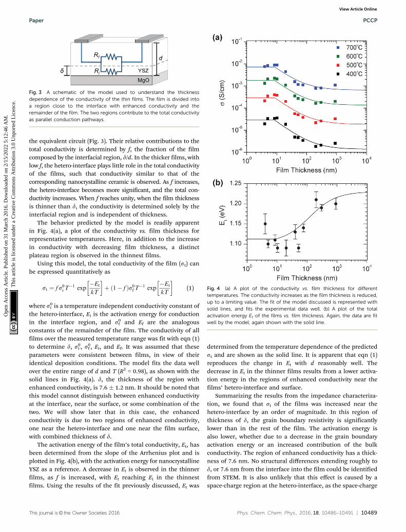
The behavior predicted by the model is readily apparentin Fig. 4(a), a plot of the conductivity vs. film thickness forrepresentative temperatures. Here, in addition to the increasein conductivity with decreasing film thickness, a distinctplateau region is observed in the thinnest films.
Using this model, the total conductivity of the film (st) canbe expressed quantitatively as
st ¼ f s0i T�1 exp
�Et
kT
� �þ ð1� f Þs0fT�1 exp
�Et
kT
� �(1)
where s0i is a temperature independent conductivity constant of
the hetero-interface, Ei is the activation energy for conductionin the interface region, and s0
f and Ef are the analogousconstants of the remainder of the film. The conductivity of allfilms over the measured temperature range was fit with eqn (1)to determine d, s0
i , s0f , Ei, and Ef. It was assumed that these
parameters were consistent between films, in view of theiridentical deposition conditions. The model fits the data wellover the entire range of d and T (R2 = 0.98), as shown with thesolid lines in Fig. 4(a). d, the thickness of the region withenhanced conductivity, is 7.6 � 1.2 nm. It should be noted thatthis model cannot distinguish between enhanced conductivityat the interface, near the surface, or some combination of thetwo. We will show later that in this case, the enhancedconductivity is due to two regions of enhanced conductivity,one near the hetero-interface and one near the film surface,with combined thickness of d.
The activation energy of the film’s total conductivity, Et, hasbeen determined from the slope of the Arrhenius plot and isplotted in Fig. 4(b), with the activation energy for nanocrystallineYSZ as a reference. A decrease in Et is observed in the thinnerfilms, as f is increased, with Et reaching Ei in the thinnestfilms. Using the results of the fit previously discussed, Et was
determined from the temperature dependence of the predictedst and are shown as the solid line. It is apparent that eqn (1)reproduces the change in Et with d reasonably well. Thedecrease in Et in the thinner films results from a lower activa-tion energy in the regions of enhanced conductivity near thefilms’ hetero-interface and surface.
Summarizing the results from the impedance characteriza-tion, we found that st of the films was increased near thehetero-interface by an order of magnitude. In this region ofthickness of d, the grain boundary resistivity is significantlylower than in the rest of the film. The activation energy isalso lower, whether due to a decrease in the grain boundaryactivation energy or an increased contribution of the bulkconductivity. The region of enhanced conductivity has a thick-ness of 7.6 nm. No structural differences extending roughly tod, or 7.6 nm from the interface into the film could be identifiedfrom STEM. It is also unlikely that this effect is caused by aspace-charge region at the hetero-interface, as the space-charge
Fig. 3 A schematic of the model used to understand the thicknessdependence of the conductivity of the thin films. The film is divided intoa region close to the interface with enhanced conductivity and theremainder of the film. The two regions contribute to the total conductivityas parallel conduction pathways.
Fig. 4 (a) A plot of the conductivity vs. film thickness for differenttemperatures. The conductivity increases as the film thickness is reduced,up to a limiting value. The fit of the model discussed is represented withsolid lines, and fits the experimental data well. (b) A plot of the totalactivation energy Et of the films vs. film thickness. Again, the data are fitwell by the model, again shown with the solid line.
Paper PCCP
Ope
n A
cces
s A
rtic
le. P
ublis
hed
on 3
1 M
arch
201
6. D
ownl
oade
d on
2/1
5/20
22 5
:12:
46 A
M.
Thi
s ar
ticle
is li
cens
ed u
nder
a C
reat
ive
Com
mon
s A
ttrib
utio
n 3.
0 U
npor
ted
Lic
ence
.View Article Online
10490 | Phys. Chem. Chem. Phys., 2016, 18, 10486--10491 This journal is© the Owner Societies 2016
thickness in 8YSZ is less than 1 nm, or by structural differencesimmediately at the interface like misfit dislocations, as theextent of these effects is much smaller than d.
Mg2+ diffusion into the grain boundary cores
We hypothesize that the grain boundary resistivity is reducedby the diffusion of Mg2+ from the MgO substrate into the grainboundary cores. Extrapolating from literature values for thediffusivity of Mg2+ in the bulk and grain boundaries of ZrO2
measured between 800 and 1000 1C, we anticipate that thatMg2+ could readily diffuse in the grain boundary cores but notin the grain interior at 700 1C, the highest temperature reachedduring thin film growth.18 This could modify the grain boundaryresistivity: as mentioned earlier, the space charge effect may playa significant role in the high grain boundary resistivity of the YSZfilms. Segregation of Mg2+ into the grain boundary core mayresult in reduction of the space-charge potential, leading toreduction in the grain boundary resistivity. This is also expectedto lead to a reduction in the activation energy in these regions,as is evident in Fig. 4. This hypothesis is supported by previousresearch: Avila-Predes and Kim19 have demonstrated that segre-gation of metal cation impurities to the grain boundary cores inGd-doped CeO2, a material similar to YSZ, reduces the grainboundary resistivity by up to an order of magnitude, whileslightly reducing the activation energy. Litzelman et al.20 inves-tigated the heterogeneous doping of nanocrystalline ceria thinfilms with Mg from a MgO substrate and an associated decreasein electronic conductivity. This was attributed to a reduction inthe grain boundary potential, reducing the concentration ofelectrons in the grain boundary’s space charge regions. For ionicconducting films, such a reduction of grain boundary potentialwould instead reduce the grain boundary resistance by reducingthe potential barrier to oxygen vacancy migration across thegrain boundaries. Thirdly, Suresh & Johnson21 reported anincrease in the total conductivity of YSZ with Mg2+ doping, alongwith segregation of Mg2+ to the grain boundaries.
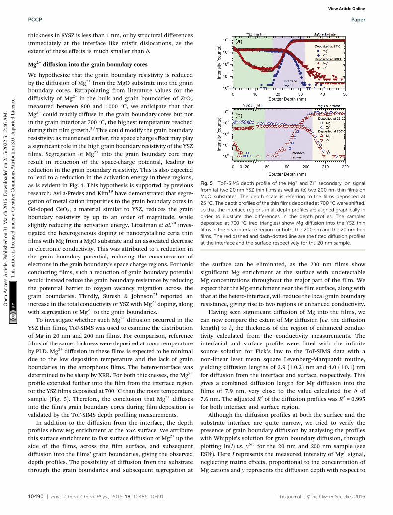
To investigate whether such Mg2+ diffusion occurred in theYSZ thin films, ToF-SIMS was used to examine the distributionof Mg in 20 nm and 200 nm films. For comparison, referencefilms of the same thickness were deposited at room temperatureby PLD. Mg2+ diffusion in these films is expected to be minimaldue to the low deposition temperature and the lack of grainboundaries in the amorphous films. The hetero-interface wasdetermined to be sharp by XRR. For both thicknesses, the Mg2+
profile extended further into the film from the interface regionfor the YSZ films deposited at 700 1C than the room temperaturesample (Fig. 5). Therefore, the conclusion that Mg2+ diffusesinto the film’s grain boundary cores during film deposition isvalidated by the ToF-SIMS depth profiling measurements.
In addition to the diffusion from the interface, the depthprofiles show Mg enrichment at the YSZ surface. We attributethis surface enrichment to fast surface diffusion of Mg2+ up theside of the films, across the film surface, and subsequentdiffusion into the films’ grain boundaries, giving the observeddepth profiles. The possibility of diffusion from the substratethrough the grain boundaries and subsequent segregation at
the surface can be eliminated, as the 200 nm films showsignificant Mg enrichment at the surface with undetectableMg concentrations throughout the major part of the film. Weexpect that the Mg enrichment near the film surface, along withthat at the hetero-interface, will reduce the local grain boundaryresistance, giving rise to two regions of enhanced conductivity.
Having seen significant diffusion of Mg into the films, wecan now compare the extent of Mg diffusion (i.e. the diffusionlength) to d, the thickness of the region of enhanced conduc-tivity calculated from the conductivity measurements. Theinterfacial and surface profile were fitted with the infinitesource solution for Fick’s law to the ToF-SIMS data with anon-linear least mean square Levenberg–Marquardt routine,yielding diffusion lengths of 3.9 (�0.2) nm and 4.0 (�0.1) nmfor diffusion from the interface and surface, respectively. Thisgives a combined diffusion length for Mg diffusion into thefilms of 7.9 nm, very close to the value calculated for d of7.6 nm. The adjusted R2 of the diffusion profiles was R2 = 0.995for both interface and surface region.
Although the diffusion profiles at both the surface and thesubstrate interface are quite narrow, we tried to verify thepresence of grain boundary diffusion by analysing the profileswith Whipple’s solution for grain boundary diffusion, throughplotting ln(I) vs. y6/5 for the 20 nm and 200 nm sample (seeESI†). Here I represents the measured intensity of Mg+ signal,neglecting matrix effects, proportional to the concentration ofMg cations and y represents the diffusion depth with respect to
Fig. 5 ToF-SIMS depth profile of the Mg+ and Zr+ secondary ion signalfrom (a) two 20 nm YSZ thin films as well as (b) two 200 nm thin films onMgO substrates. The depth scale is referring to the films deposited at25 1C. The depth profiles of the thin films deposited at 700 1C were shifted,so that the interface regions in all depth profiles are aligned graphically inorder to illustrate the differences in the depth profiles. The samplesdeposited at 700 1C (red triangles) show Mg diffusion into the YSZ thinfilms in the near interface region for both, the 200 nm and the 20 nm thinfilms. The red dashed and dash-dotted line are the fitted diffusion profilesat the interface and the surface respectively for the 20 nm sample.
PCCP Paper
Ope
n A
cces
s A
rtic
le. P
ublis
hed
on 3
1 M
arch
201
6. D
ownl
oade
d on
2/1
5/20
22 5
:12:
46 A
M.
Thi
s ar
ticle
is li
cens
ed u
nder
a C
reat
ive
Com
mon
s A
ttrib
utio
n 3.
0 U
npor
ted
Lic
ence
.View Article Online

This journal is© the Owner Societies 2016 Phys. Chem. Chem. Phys., 2016, 18, 10486--10491 | 10491
the interface under investigation. If diffusion from the MgOsubstrate primarily takes place in the grain boundaries, theprofile gives a straight line for ln(I) vs. y6/5.22 At the surface ofthe 20 nm sample, the plot versus y6/5 indeed shows a linearcourse in the surface region. However, the interface diffusionprofile does not show linear behaviour. The same holds for theinterface profile of the 200 nm sample. The Mg intensity at the200 nm sample surface was to narrow for any analysis. Weconclude that there is clear evidence of grain boundary diffu-sion from the surface, but the mechanism of the diffusion fromthe substrate remains unclear. In view of the restricted data set,we consider these results with care and take this as highlyinteresting motivation to extend the diffusion studies and theiranalysis by SIMS. Thus, in order to gain deeper insight into thediffusion of Mg into the YSZ thin films further studies are requiredand planned. Notwithstanding, the width of the region of signifi-
cant Mg concentration the diffusion length 2ffiffiffiffiffiffiDtp
obtained fromthe infinite source solution is a good measure in order to quantifythe thickness of the Mg enriched region – irrespective of the detailsof the quantitative analysis of the profiles. The good agreementbetween the two, the proposed model and the ToF-SIMS measure-ments provides strong evidence that the Mg diffusion is the sourceof the reduced grain boundary resistance and enhanced conduc-tivity observed in these thin films.
Conclusions
In summary, thin films with nano-columnar grains were depos-ited and characterized. The conductivity in the thinnest filmswas enhanced by an order of magnitude relative to the thickerfilms and comparable to that of single crystal YSZ. Theenhanced conductivity was attributed to a reduction of thegrain boundary resistivity near the thin film interface in aregion of roughly 8 nm. Based on this length-scale, surfaceand interfacial space-charge effects and structural differences wereeliminated as the source of reduced grain boundary resistivity. Weattribute the enhancement in conductivity to diffusion of Mg2+
from MgO substrate into the grain boundaries, which was verifiedby ToF-SIMS depth profiling. Future work in extending this effect tothicker films or bulk materials appears promising. These resultsdemonstrate the importance of grain boundaries in understandingthe ionic conductivity of electrolyte thin films, as well as themitigation of their blocking effect due to chemical diffusion nearthe hetero-interface.
Acknowledgements
We gratefully acknowledge many valuable discussions aboutToF-SIMS measurements with Dr Marcus Rohnke. S. K. wishesto thank the US-Israel Binational Science Foundation forfunding this research. Y. T. would like to acknowledge NSFfor financial support (DMR 747896). JJ and MKB acknowledge
financial support by DFG (Deutsche Forchungsgemeinschaft)within the project DFG Ja 648/21-1. N. B. acknowledges supportthrough the Laboratory Directed Research and Development(LDRD) Program Chemical Imaging Initiative (CII) at PacificNorthwest National Laboratory (PNNL) and the EnvironmentalMolecular Sciences Laboratory (EMSL), a national scientificuser facility sponsored by DOE’s Office of Biological andEnvironmental Research (BER) at PNNL. PNNL is a multiprogramnational laboratory operated by Battelle for DOE under ContractDE-AC05-76RL01830.
Notes and references
1 E. D. Wachsman and K. T. Lee, Science, 2011, 334, 935–939.2 H. Aydin, C. Korte, M. Rohnke and J. Janek, Phys. Chem.
Chem. Phys., 2013, 15, 1944–1955.3 E. Fabbri, D. Pergolesi and E. Traversa, Sci. Technol. Adv.
Mater., 2010, 11, 054503.4 B. Zhu, Int. J. Energy Res., 2009, 33, 1126–1137.5 X. Guo and J. Maier, J. Electrochem. Soc., 2001, 148, E121.6 X. Guo and R. Waser, Prog. Mater. Sci., 2006, 51, 151–210.7 C. Korte, N. Schichtel, D. Hesse and J. Janek, Monats.
Chem. – Chemical Monthly, 2009, 140, 1069–1080.8 S. Jiang and J. B. Wagner Jr, J. Phys. Chem. Solids, 1994, 56,
1101–1111.9 X. Wang, Y. Ma, S. Li, A.-H. Kashyout, B. Zhu and
M. Muhammed, J. Power Sources, 2011, 196, 2754–2758.10 I. Kosacki, C. Rouleau, P. Becher, J. Bentley and D. Lowndes,
Solid State Ionics, 2005, 176, 1319–1326.11 J. Garcia-Barriocanal, A. Rivera-Calzada, M. Varela,
Z. Sefrioui, E. Iborra, C. Leon, S. J. Pennycook andJ. Santamaria, Science, 2008, 321, 676–680.
12 J. K. C. Korte, A. Peters, N. Schichtel, H. Aydin and J. Janek,Phys. Chem. Chem. Phys., 2014, 16, 24575.
13 M. Sillassen, P. Eklund, N. Pryds, E. Johnson, U. Helmerssonand J. Bøttiger, Adv. Funct. Mater., 2010, 20, 2071–2076.
14 J. Jiang and J. L. Hertz, J. Electroceram., 2013, 32, 37–46.15 A. Infortuna, A. S. Harvey and L. J. Gauckler, Adv. Funct.
Mater., 2008, 18, 127–135.16 T. J. K. Takanori Kiguchi, H. Funakubo, O. Sakurai and
K. Shinozaki, J. Ceram. Soc. Jpn., 2013, 122, 72–77.17 Leptos Manual, Bruker AXS, WI, 2005.18 T. Bak, J. Nowotny, K. Prince, M. Rekas and C. C. Sorrell,
J. Am. Ceram. Soc., 2002, 85, 2244–2250.19 H. Avilaparedes and S. Kim, Solid State Ionics, 2006, 177,
3075–3080.20 S. J. Litzelman, R. A. De Souza, B. Butz, H. L. Tuller, M. Martin
and D. Gerthsen, J. Electroceram., 2008, 22, 405–415.21 M. B. Suresh and R. Johnson, Int. J. Energy Res., 2012, 36,
1291–1297.22 D. Gryaznov, J. Fleig and J. Maier, Defect Diffus. Forum, 2005,
237–240, 1043–1048.
Paper PCCP
Ope
n A
cces
s A
rtic
le. P
ublis
hed
on 3
1 M
arch
201
6. D
ownl
oade
d on
2/1
5/20
22 5
:12:
46 A
M.
Thi
s ar
ticle
is li
cens
ed u
nder
a C
reat
ive
Com
mon
s A
ttrib
utio
n 3.
0 U
npor
ted
Lic
ence
.View Article Online