Homework Week 4: Thermoelectric Systems Thermoelectricity ...

MATENER 2018
Javier Rodríguez-Viejo
Physics Department
Universitat Autònoma de Barcelona
Thermoelectricity I
(tutorial & inorganic TE materials)
ICMAB, Bellaterra 20 September 2018

OVERVIEW
Basics and General Introduction.
Concepts. Figure of Merit.
Strategies to reduce thermal conductivity
Strategies to increase power factor
A short view on inorganic materials
Thermoelectric Devices & Applications
Javier Rodríguez MATENER2018

ENERGY SOURCES
Source: Kartounen

Clean energy sources
Thermoelectric generation is still behind solar cell and fuel cell technologies
but
still useful to partially recover waste heat generated by combustion engines

Principle
KINETIC THEORY
T
ThTc
𝐽𝑇 ∝ 𝛻𝑇
Gas particles
in equilibrium

𝐽𝑇 ∝ 𝛻𝑇
𝐽𝐶 ∝ 𝛻𝑐
If particles are charged In steady stateTh
Tc
-- --
-
-
--
-
--
-- -
--
--
----
--
--- -
--
-
-
--
----
-
-
--
-
-- --
--
-
-
-- -
--
-
In steady stateTh
Tc
𝐽𝑇 = 𝐽𝐶
𝐽𝑇 ∝ 𝛻𝑇
𝐽𝐸 ∝ 𝛻𝐸
𝐽𝑇 = 𝐽𝐸

In steady stateTh
Tc
-- --
-
-
--
-
--
-- -
--
--
----
--
--- -
--
-
-
--
----
-
-
--
-
-- --
--
-
-
-- -
--
-
V
Seebeck voltage (1821)
When a T exists in bar a voltage
develops between the two ends.
Seebeck voltage is the steady-state
voltageaccumulated under the open
circuit conditions
+ -
ΔV>0
𝑆 = −𝑉ℎ − 𝑉𝑐𝑇ℎ − 𝑇𝑐
= −∆𝑉
𝑇ℎ − 𝑇𝑐
S > 0 p-type
S < 0 n-type
Except in very
specific cases when
slope is negative
𝜕 log 𝜎(𝜀)
𝜕𝐸<0

Thermoelectric Generation
Power output
S thermopower
σ electrical conductivity
κ thermal conductivity
Tk
SZT
2
The idoneity of a TE material
can be evaluated by
FIGURE OF MERIT

FIGURE of MERIT & EFFICIENCY
Carnot efficiency
Thermoelectric efficiency
c
chC
T
TT
h
cCTE
T
TZT
ZT
1
11
Gayner, Kar, PMS (2016)

Large scale
Hig
h-T
Impact of ZT on power applications
Small scale
Lo
w-T
Medium
C.B.Vining, Nature 2009
Advantages: No moving parts, little maintenance, no greenhouse gas emission
Vining, Nature 2009

Good heat conductors
are
good electrical conductors
10-2 10-1 1 10 102 103W/mK
SiliconGlassWood
Graphene
Copper
Air
Stainless
steel
10-2 10-1 1 10 102 103W/mK
SiliconGlassWood
Graphene
Copper
10-2 10-1 1 10 102 10310-2 10-1 1 10 102 103W/mK
SiliconGlassWood
Graphene
Copper
Air
Stainless
steel
k=kl+ke:
metals have lots of free electrons
(ke is large), while ceramics
have few (only kl is active)
High efficiency
requires maximizing ZT
Increase in S2σ
Decrease in κPHONON GLASS
ELECTRON CONDUCTOR
No such material exists in Nature !!!
(Slack, 1994)
Tk
SZT
2

Large values of ZT require high S, high and low Difficult to accomplish
S
Wiedemann-Franz law
Tuning Seebeck, thermal & electrical conductivity
Zeier et al. Nat. Rev. Mat., 2016
SZT
σ
klatkel
S2σ

Strategies to reduce thermal conductivity
Phonons (heat carriers)
Quantized energy of lattice vibration
𝐸 = ℏ𝜔 = ℎ𝑐
𝜆
Based on spring and mass system
Phonons scattered whenever there
is a difference
in mass and/or spring constant.

Reducing without affecting S and is realized in semiconductors of
high atomic weigth which reduces the speed of sound in the material and therefore .
1950–1959: Ioffe stated that the thermal conductivity of semiconductors is a
function of atomic weight. Generally, elements with large atomic weights have
low thermal conductivity.
STRATEGY USED 1950-1990
Heavy mass-concept
BiTe
PbTe
SbTe
and alloys
𝑘 =1
3𝐶 ∙ 𝑣 ∙ 𝑙

Engineering phonon thermal transport
Reducing k without as much reduction of σ and S

Engineering phonon thermal transport
𝜅𝑙𝑎𝑡 =1
3∙ 𝐶 𝜔 ∙ 𝑙 𝜔 ∙ 𝑣 𝜔 ∙ 𝑑𝜔
Yang et al. Adv. Energy Mat. 2017
Grain-boundary
scattering
Impurity scattering
scattering

If T > Q, C ~ constant
Specific heat
Size-effects: useful at very low-T’s
Size of the crystal is of atomic scale so
lattice vibrations are confined and
dispersion relation is modified
𝐶𝑉 =𝜕𝐸𝑝ℎ𝜕𝑇
𝑉
If T << Q, C ~ T d (d: dimension)
Debye-like regime T3

Phonon group velocity
i) Increasing the number of atoms in the unit cell
𝑣 =𝑑𝜔
𝑑𝑞
Optical branches:
Small sound velocity
𝑐𝑠𝑜𝑢𝑛𝑑 =𝑑𝜔
𝑑𝑞𝑞=0
=𝐸
𝜌
ii) Heavy atoms iii) Periodic structures with sizes ≈ λph (few nm)
Phonon bandgaps
lower v

Phonon mean free path (average distance between collisions)
short-wavelength phonon
long-wavelength phonon
Phon
on
mea
n f
ree p
ath
(nm
)
1 10
103
101
10-1
Phonon Frequency (THz)
c-Si
At room T
Wavelength
Dominant heat-
carrying 5-10 nm
but broadband
Mean freepath
10-100’s nm
ELECTRONS
Mean freepath
1-5 nm
PHONONS
Wavelength
1-3 nm

Long 𝜆 phonons carry most heat at low T
Boundary scatt. at low-T
As T increases 𝜆𝑝ℎ dominant phonons
decreases
At high T ph-ph scattering
𝜆𝑚𝑎𝑥 ∙ 𝑇 ≈ 𝑐𝑡𝑒
Wien’s law holds for phonons
1
𝑙𝑒𝑓𝑓=1
𝑙𝑏+1
𝑙𝑖+1
𝑙𝑝ℎ
lb boundary scattering
li impurity scattering
lph phonon-phonon scattering

ALLOY LIMIT
Alloys: Lowest thermal conductivity in crystalline solids.
Atomic substitutions heavily scatter phonons
Rayleig scattering regime: scattering cross section
σ ~ b6/λ4
If atoms have b ~ 1Å Alloys scatter short-wave phonons more effectively
than mid-long-wave phonons
TOWARDS LOW THERMAL CONDUCTIVITY
DECREASING THE MEAN FREE PATH OF PHONONS:

ALLOYING
Mass disorder induces
strong reduction
of thermal conductivity
Maximum variation below 10 at % Ge
k constant between 20-70 at % Ge
0 0.2 0.4 0.6 0.8 1
~150 W/mK
~60 W/mK
~10 W/mK
Ge Composition
Ther
mal
con
du
ctiv
ity
bulk
Thin films
Mainly affects short-wavelength
(high frequency)phonons
If mid- to long-phonons could be scatterered, then alloy limit can be beaten !!!!!!
𝜅𝑙𝑎𝑡 =1
3∙ 𝐶 𝜔 ∙ 𝑙 𝜔 ∙ 𝑣 𝜔 ∙ 𝑑𝜔

THIN FILMS & SUPERLATTICES
SL
QD SL
Maximizing dot coverageDiminishing period in QDSL
Surface segregation SLSurface seggregation SL
SL
QDSL
Maximize dot coverageReduce period
Phonon-blocking/electron transmitting interfaces
in Si/Ge and other SLs
Use of the acoustic mismatch between the
SL components to reduce ph.
TF-SL

Thin films of Si Goodson et al., APL. 74, 3005 (1999)
Thin films of SiGe alloys
Cheaito et al. PRL 2012
UAB & ICMAB collaboration Nano Research 2017
SiGe Superlattices

Thermal conductivity of Ge Quantum Dot Superlattices
0 50 100 150 200 250 3000123456789
1011121314151617
0 10 20 30 40 50 60 70 80
Inte
nsity
(arb
. units
)
Therm
al C
onductivity (
W/m
*K)
Temperature (K)
(a)
Raman shift (cm-1
)
(b)
UAB-ICMAB collaboration, APL 2008

Increase boundary scattering of phonons at the barrier-well interfaces,
without as large increase in electron scattering at the interface
while keeping
If the width of the semiconductor is smaller than the mean free path of phonons
and larger than that of electrons or holes
Lower-D MATERIALS (nanowires)

Embedded nanostructures in semiconductor alloys
scatter the mid-to-long wavelength phonons more efficiently because
the similarity in sizes, reducing k below the alloy limit.
AgPb18SbTe20 Hsu et al. Science 303 (2004)
nanodot
Ag-Sb-rich
klat = 1.30 W/mK at 300 K < bulk PbTe
Kim et al. PRL 2006
Reduction by 2 below alloy limit
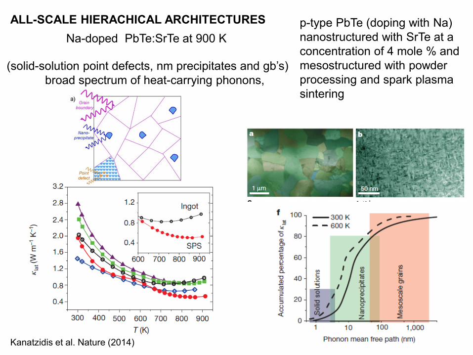
ALL-SCALE HIERACHICAL ARCHITECTURES
Kanatzidis et al. Nature (2014)
p-type PbTe (doping with Na)
nanostructured with SrTe at a
concentration of 4 mole % and
mesostructured with powder
processing and spark plasma
sintering
(solid-solution point defects, nm precipitates and gb’s)
broad spectrum of heat-carrying phonons,
Na-doped PbTe:SrTe at 900 K

Grown by electron beam
Below the amorphous limit: Taking benefit of interfaces
J. Alvarez-Quintana et al. J.Appl. Phys. 2009
Increasing effect of interfaces
t
Rk
kk
thlayers
layers
eff
1
W/Al2O3 nanolaminate with layers few nm thick
and
high density of interfaces has
κ < amorphous limit
Costescu and Cahill et al. Science 2005

Cahill et al. Science 2007
Ultralow k in VdW stacks
Sequential bilayers of W and Se by MBE + 1h annealing
for layered WSe2 structure
k(300K)=0.048 W/mK
6 times smalles than amorphous limit
VdW interaction between WSe2 adjacent layers +
+ disorder in c-axis induces phonon localization
WSe2

Nanostructured material: HOLEY SILICON
Tang et al. Nano Letters 2010

Strategies to increase power factor
S2 σ
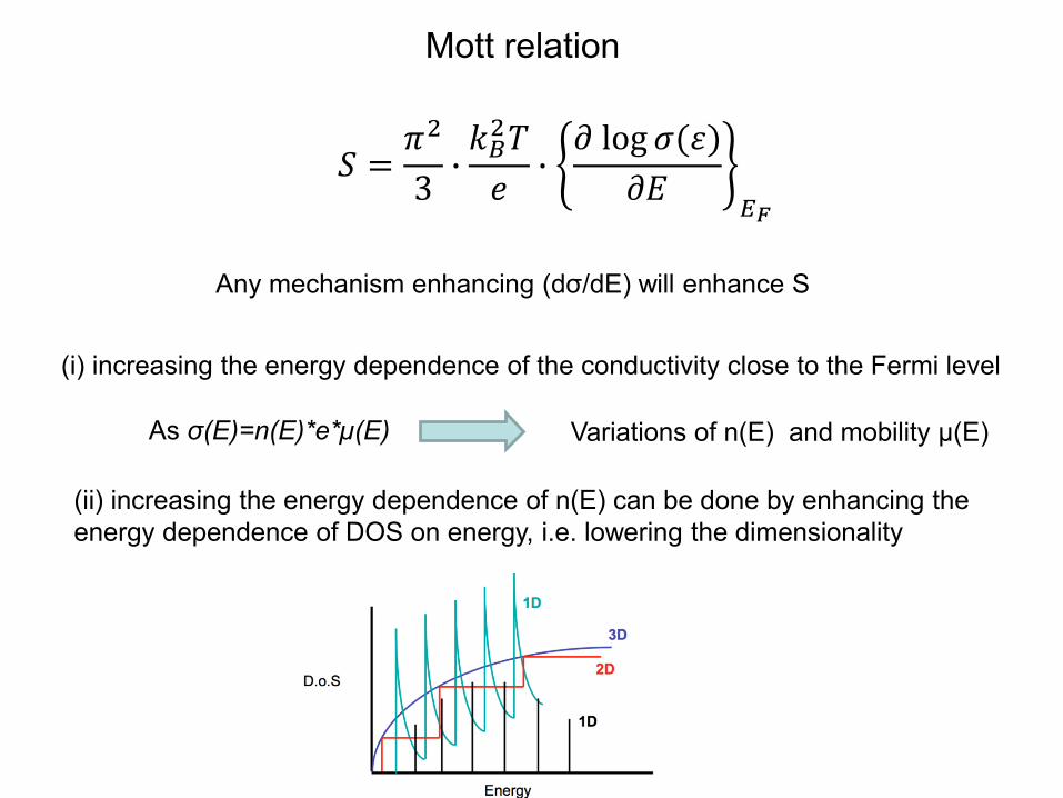
(i) increasing the energy dependence of the conductivity close to the Fermi level
Mott relation
𝑆 =𝜋2
3∙𝑘𝐵2𝑇
𝑒∙𝜕 log 𝜎(𝜀)
𝜕𝐸𝐸𝐹
Any mechanism enhancing (dσ/dE) will enhance S
As σ(E)=n(E)*e*µ(E) Variations of n(E) and mobility µ(E)
(ii) increasing the energy dependence of n(E) can be done by enhancing the
energy dependence of DOS on energy, i.e. lowering the dimensionality
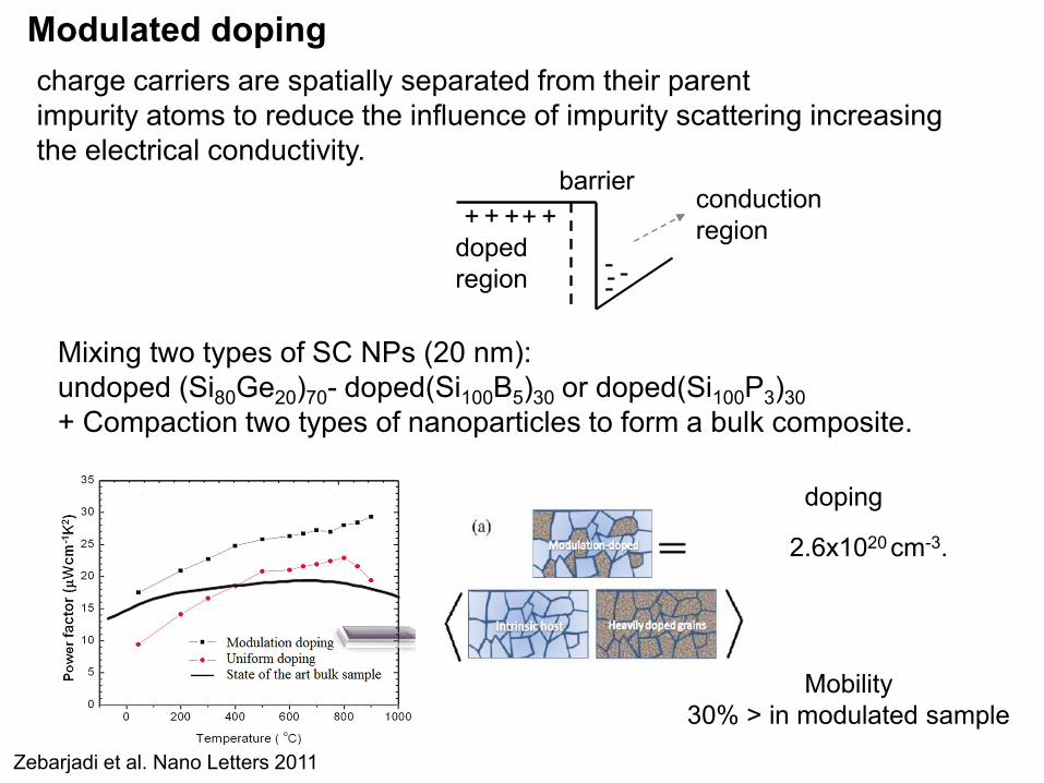
Modulated doping
Zebarjadi et al. Nano Letters 2011
Mixing two types of SC NPs (20 nm):
undoped (Si80Ge20)70- doped(Si100B5)30 or doped(Si100P3)30
+ Compaction two types of nanoparticles to form a bulk composite.
charge carriers are spatially separated from their parent
impurity atoms to reduce the influence of impurity scattering increasing
the electrical conductivity.
2.6x1020 cm-3.
doping
Mobility
30% > in modulated sample
barrier
-- --
+ + ++ +
doped
region
conduction
region

Energy Filtering (I)
As T increases bipolar k increases lowering S
Shakouri et al. APL 2014
In the intrinsic regime
Blocking minority carriers
Concept
SLs or NP embedded in matrix
Minority carrier blocking
Relevant for small Eg materials at high T

Second-phase NPs or specific barriers
(gb & others) can serve as potential barriers
that prohibit low energy carriers from
passing through the barriers
Energy Filtering (II)
increase Seebeck coefficient
Yb-filled CoSb3
Hot carrier filtering
Calculation for p-SiGe
Minnich et al. En. Env. Sci. 2009
By filtering low-energy carriers
average carrier energy increased

TE MATERIALS
Gayner, Kar, PMS (2016)

Nanostructured materials. Case of SiGe
SiGe alloys: traditional material for high T Applications (T>800oC)
Can be doped n- and p-type enabling complete TE devices in one platform
Fabrication: BM + HP
Joshi et al. Nano Letters, 2009
Si80Ge20 with grain sizes about 20 nm
Increased phonon scattering
at interfaces and defects
Increase ZT is a general feature
in nanograin materials
p-type SiGe
bulk alloy
n-type ZT up to 1.5 at T=1173 K
p-type ZT up to 0.95
Yu, Nano Letters 2012

Skutterudites‘‘skutterudite” refers to naturally occurring mineral CoAs3,
first discovered in Skutterud, Norway.
Cubic structure composed of 32 atoms per unit cell
CoAs3 exhibits a distorted version of the AB3-type perovskite
structure, that is, MX3 (M = Co, Rh, Ir is a group 9 transition
metal and X a group 15 nonmetal P, As, Sb), with an
octahedral structure and a void at its center.
The void-filling atom can act as an electron donor or electron acceptor.
Strong phonon scattering centers reduce k.
Good thermal and mechan. properties of both n- and p-type operating at medium T
Key aspects:
Filling the void fulfills PGEC-concept such as in CeFe4Sb12
PF=6.5 µW/cmK-2, k=10 W/mK
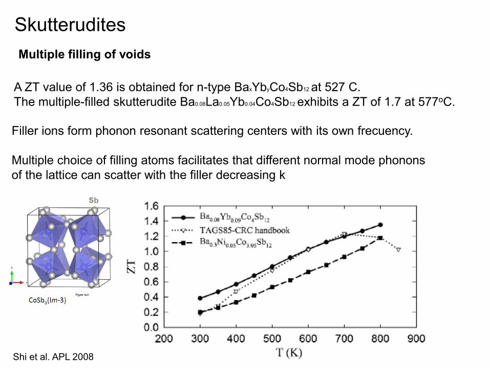
A ZT value of 1.36 is obtained for n-type BaxYbyCo4Sb12 at 527 C.
The multiple-filled skutterudite Ba0.08La0.05Yb0.04Co4Sb12 exhibits a ZT of 1.7 at 577oC.
Skutterudites
Multiple filling of voids
Shi et al. APL 2008
Filler ions form phonon resonant scattering centers with its own frecuency.
Multiple choice of filling atoms facilitates that different normal mode phonons
of the lattice can scatter with the filler decreasing k
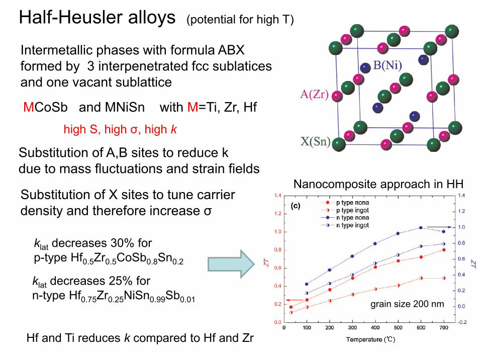
Intermetallic phases with formula ABX
formed by 3 interpenetrated fcc sublatices
and one vacant sublattice
MCoSb and MNiSn with M=Ti, Zr, Hf
Substitution of A,B sites to reduce k
due to mass fluctuations and strain fields
Substitution of X sites to tune carrier
density and therefore increase σ
Hf and Ti reduces k compared to Hf and Zr
Nanocomposite approach in HH
klat decreases 30% for
p-type Hf0.5Zr0.5CoSb0.8Sn0.2
klat decreases 25% for
n-type Hf0.75Zr0.25NiSn0.99Sb0.01grain size 200 nm
Half-Heusler alloys (potential for high T)
high S, high σ, high k

Single-Crystal SnSe Simultaneous low k and higher power factor
SnSe does not have high MW,
nanostructuring,
a complex crystal structure
or a large unit cell.
Power factor increase
to 40 µW cm-1 K-2
Orthorombic structure
Complex electronic structure
ZT=2.6 at 973 K
𝑆 =𝜋2
3∙𝑘𝐵2𝑇
𝑒∙𝜕 log 𝜎(𝜀)
𝜕𝐸𝐸𝐹
Zhao et al. Nature 2014, Science 2015 and En. Environ. Sci. (2016)
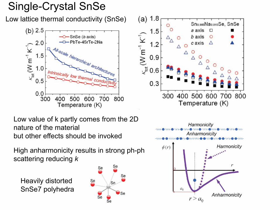
Low lattice thermal conductivity (SnSe)
Low value of k partly comes from the 2D
nature of the material
but other effects should be invoked
High anharmonicity results in strong ph-ph
scattering reducing k
Heavily distorted
SnSe7 polyhedra
Single-Crystal SnSe

Single-Crystal SnSe

p n p n
Cold plate
Heat source
Heat sink
Electrical Power output
p n p n
Cold plate
Heat source
Heat sink
Electrical Power output
APPLICATIONS
TE generators: Set of n,p legs electrically connected in series
and thermally in parallel
Apart from thermoelectric materials, contact
materials also play a key role in TE devices.
The semiconductor–metal junction exhibits a
greater electrical resistance than a metal–
metal junction, which affects the performance
of the device

Radioisotope thermoelectric generators, RTGs
Heat provided by radioisotope decay
Th: 800-1200oC
TE material: SiGe
Efficiency < 8%Power output:
from mW to 100’s W depending on size
Specific power: skutter. 4W/kg; SiGe: 4-5 W/kg
ZT of 0.5 (p-type) and 0.9 (n-type)
Yang, Adv. Energy Mat. 2017

Solar Thermal Power Generation (STEG’s)
Yang, Adv. Energy Mat. 2017

AUTOMOTIVE TEG’s
T=800oC
T=200oC
Orr et al. App. Thermal Eng. 2016
400 W with 4.6 kg of TE material
Still in concept stages
Goal total of 750 W from 20 W TEGs
Honda prototype with líquid cooler gives 500 W
32 30 mmx 30 mm TEGs

Microthermoelectric TE-based generators/sensors
UAB, Nano Energy 2015
0,00 0,01 0,02 0,03
0,0
1,0
2,0
3,0
4,0
5,0T~ 25K T~ 50K T~ 75K
T~ 100K T~ 150K T~ 200K
Pow
er
de
nsity (
mW
/cm
2)
Current (mA)
0,0
0,4
0,8
1,2
1,6
2,0
Volta
ge
(V)
0,0 0,2 0,4 0,6 0,8 1,0 1,20
1
2
3
4
5
1.3 K
1.9 K
2.5 K
3.2 K
4.7 K
5.5 K
Po
we
r d
en
sity (
W
/cm
2)
I (A)
T
Low-d Si thermopilesSize: 3x3 mm2

Low Power: using body heat
Thermoelectric watch

SENSING APPLICATIONS
Yang, Adv. Energy Mat. 2017
Detecting heat signals from catalytic reactions
Pt thin film acts as a catalyst for the reaction with H2,
releasing heat amd creating a T difference
Good sensitivity and short response time
Other catalyst can be used for other gases

On-chip cooling using SL’s
Creation of a heat difference from an
electric voltage
Heat carried by carriersIQ /
Peltier effect
Choudhury et al. Nat. Nanotech 2007
Venkatasubramanian et al. Nature, (2001) 597-.


CONCLUSIONS
Reducing k below the alloy limit may require new strategies such as
reduction of the phonon group velocity or reducing the number of
phonon modes that propagate.
Anharmonicity may play a significant role for decreasing k.
Many of strategies to increase ZT. However, ZT above 3 in both n- and
p-type materials (required for some dreamed applications of energy
harvesting) still far to be realized.
Still PLENTY of ROOM for IMPROVEMENT
In spite of this there are many opportunities for low-power applications to
power sensor or low-consumption devices.

THANK YOU
![Institute of Thermoelectricity, Academy of Sciences and ...jt.inst.cv.ua/jt/jt_2017_01_en.pdfcontinuation of research on the history of thermoelectricity in Russia [4-7]. Below we](https://static.fdocuments.in/doc/165x107/60b8a2425a50b440ca20bf2b/institute-of-thermoelectricity-academy-of-sciences-and-jtinstcvuajtjt201701enpdf.jpg)